KR102445111B1 - Semiconductor device and method of manufacturing semiconductor device - Google Patents
Semiconductor device and method of manufacturing semiconductor device Download PDFInfo
- Publication number
- KR102445111B1 KR102445111B1 KR1020207036261A KR20207036261A KR102445111B1 KR 102445111 B1 KR102445111 B1 KR 102445111B1 KR 1020207036261 A KR1020207036261 A KR 1020207036261A KR 20207036261 A KR20207036261 A KR 20207036261A KR 102445111 B1 KR102445111 B1 KR 102445111B1
- Authority
- KR
- South Korea
- Prior art keywords
- semiconductor device
- conductive
- conductive heat
- heat
- conducting member
- Prior art date
Links
- 239000004065 semiconductor Substances 0.000 title claims abstract description 165
- 238000004519 manufacturing process Methods 0.000 title claims description 27
- 238000001816 cooling Methods 0.000 claims abstract description 42
- 229920005989 resin Polymers 0.000 claims abstract description 36
- 239000011347 resin Substances 0.000 claims abstract description 36
- 239000000758 substrate Substances 0.000 claims abstract description 28
- 239000011231 conductive filler Substances 0.000 claims description 38
- 238000000034 method Methods 0.000 claims description 24
- 229920000049 Carbon (fiber) Polymers 0.000 claims description 11
- 239000004917 carbon fiber Substances 0.000 claims description 11
- VNWKTOKETHGBQD-UHFFFAOYSA-N methane Chemical group C VNWKTOKETHGBQD-UHFFFAOYSA-N 0.000 claims description 7
- 238000003825 pressing Methods 0.000 claims description 3
- 230000001629 suppression Effects 0.000 abstract description 33
- 230000017525 heat dissipation Effects 0.000 abstract description 28
- 229910052751 metal Inorganic materials 0.000 description 25
- 239000002184 metal Substances 0.000 description 25
- 239000000843 powder Substances 0.000 description 23
- 229920001296 polysiloxane Polymers 0.000 description 17
- 239000002245 particle Substances 0.000 description 13
- 239000011230 binding agent Substances 0.000 description 12
- 239000011256 inorganic filler Substances 0.000 description 12
- 229910003475 inorganic filler Inorganic materials 0.000 description 12
- 239000003795 chemical substances by application Substances 0.000 description 11
- 230000005684 electric field Effects 0.000 description 11
- 238000004458 analytical method Methods 0.000 description 10
- 239000000463 material Substances 0.000 description 10
- 239000000835 fiber Substances 0.000 description 8
- PNEYBMLMFCGWSK-UHFFFAOYSA-N aluminium oxide Inorganic materials [O-2].[O-2].[O-2].[Al+3].[Al+3] PNEYBMLMFCGWSK-UHFFFAOYSA-N 0.000 description 7
- 230000000052 comparative effect Effects 0.000 description 7
- PMHQVHHXPFUNSP-UHFFFAOYSA-M copper(1+);methylsulfanylmethane;bromide Chemical compound Br[Cu].CSC PMHQVHHXPFUNSP-UHFFFAOYSA-M 0.000 description 6
- 238000010586 diagram Methods 0.000 description 6
- 239000006247 magnetic powder Substances 0.000 description 6
- VYPSYNLAJGMNEJ-UHFFFAOYSA-N Silicium dioxide Chemical compound O=[Si]=O VYPSYNLAJGMNEJ-UHFFFAOYSA-N 0.000 description 5
- 238000007259 addition reaction Methods 0.000 description 5
- 229920001971 elastomer Polymers 0.000 description 5
- 239000006249 magnetic particle Substances 0.000 description 5
- 239000005060 rubber Substances 0.000 description 5
- 229920001187 thermosetting polymer Polymers 0.000 description 5
- OKTJSMMVPCPJKN-UHFFFAOYSA-N Carbon Chemical compound [C] OKTJSMMVPCPJKN-UHFFFAOYSA-N 0.000 description 4
- RYGMFSIKBFXOCR-UHFFFAOYSA-N Copper Chemical compound [Cu] RYGMFSIKBFXOCR-UHFFFAOYSA-N 0.000 description 4
- XLOMVQKBTHCTTD-UHFFFAOYSA-N Zinc monoxide Chemical compound [Zn]=O XLOMVQKBTHCTTD-UHFFFAOYSA-N 0.000 description 4
- 238000010521 absorption reaction Methods 0.000 description 4
- 229910052782 aluminium Inorganic materials 0.000 description 4
- XAGFODPZIPBFFR-UHFFFAOYSA-N aluminium Chemical compound [Al] XAGFODPZIPBFFR-UHFFFAOYSA-N 0.000 description 4
- 229910052802 copper Inorganic materials 0.000 description 4
- 239000010949 copper Substances 0.000 description 4
- 230000000694 effects Effects 0.000 description 4
- 230000006872 improvement Effects 0.000 description 4
- 230000008569 process Effects 0.000 description 4
- 238000011282 treatment Methods 0.000 description 4
- XEEYBQQBJWHFJM-UHFFFAOYSA-N Iron Chemical compound [Fe] XEEYBQQBJWHFJM-UHFFFAOYSA-N 0.000 description 3
- 229910000808 amorphous metal alloy Inorganic materials 0.000 description 3
- 238000000889 atomisation Methods 0.000 description 3
- 230000008901 benefit Effects 0.000 description 3
- 238000004364 calculation method Methods 0.000 description 3
- 239000012295 chemical reaction liquid Substances 0.000 description 3
- 239000000945 filler Substances 0.000 description 3
- 229910002804 graphite Inorganic materials 0.000 description 3
- 239000010439 graphite Substances 0.000 description 3
- 239000007788 liquid Substances 0.000 description 3
- 239000000203 mixture Substances 0.000 description 3
- IJGRMHOSHXDMSA-UHFFFAOYSA-N Atomic nitrogen Chemical compound N#N IJGRMHOSHXDMSA-UHFFFAOYSA-N 0.000 description 2
- 229910052582 BN Inorganic materials 0.000 description 2
- PZNSFCLAULLKQX-UHFFFAOYSA-N Boron nitride Chemical compound N#B PZNSFCLAULLKQX-UHFFFAOYSA-N 0.000 description 2
- 229920000459 Nitrile rubber Polymers 0.000 description 2
- 229910008423 Si—B Inorganic materials 0.000 description 2
- GWEVSGVZZGPLCZ-UHFFFAOYSA-N Titan oxide Chemical compound O=[Ti]=O GWEVSGVZZGPLCZ-UHFFFAOYSA-N 0.000 description 2
- 230000000903 blocking effect Effects 0.000 description 2
- 125000002915 carbonyl group Chemical group [*:2]C([*:1])=O 0.000 description 2
- 238000005229 chemical vapour deposition Methods 0.000 description 2
- 238000013329 compounding Methods 0.000 description 2
- 238000013461 design Methods 0.000 description 2
- 238000011161 development Methods 0.000 description 2
- 230000005672 electromagnetic field Effects 0.000 description 2
- 238000011156 evaluation Methods 0.000 description 2
- 125000000524 functional group Chemical group 0.000 description 2
- 239000007769 metal material Substances 0.000 description 2
- 239000005300 metallic glass Substances 0.000 description 2
- 150000002739 metals Chemical class 0.000 description 2
- 238000002156 mixing Methods 0.000 description 2
- TWNQGVIAIRXVLR-UHFFFAOYSA-N oxo(oxoalumanyloxy)alumane Chemical compound O=[Al]O[Al]=O TWNQGVIAIRXVLR-UHFFFAOYSA-N 0.000 description 2
- 230000035699 permeability Effects 0.000 description 2
- 229920001721 polyimide Polymers 0.000 description 2
- 229920001955 polyphenylene ether Polymers 0.000 description 2
- 230000009467 reduction Effects 0.000 description 2
- HBMJWWWQQXIZIP-UHFFFAOYSA-N silicon carbide Chemical compound [Si+]#[C-] HBMJWWWQQXIZIP-UHFFFAOYSA-N 0.000 description 2
- 229910010271 silicon carbide Inorganic materials 0.000 description 2
- 239000000377 silicon dioxide Substances 0.000 description 2
- 239000002356 single layer Substances 0.000 description 2
- 238000004381 surface treatment Methods 0.000 description 2
- 238000004073 vulcanization Methods 0.000 description 2
- 239000011787 zinc oxide Substances 0.000 description 2
- XQUPVDVFXZDTLT-UHFFFAOYSA-N 1-[4-[[4-(2,5-dioxopyrrol-1-yl)phenyl]methyl]phenyl]pyrrole-2,5-dione Chemical compound O=C1C=CC(=O)N1C(C=C1)=CC=C1CC1=CC=C(N2C(C=CC2=O)=O)C=C1 XQUPVDVFXZDTLT-UHFFFAOYSA-N 0.000 description 1
- RNFJDJUURJAICM-UHFFFAOYSA-N 2,2,4,4,6,6-hexaphenoxy-1,3,5-triaza-2$l^{5},4$l^{5},6$l^{5}-triphosphacyclohexa-1,3,5-triene Chemical compound N=1P(OC=2C=CC=CC=2)(OC=2C=CC=CC=2)=NP(OC=2C=CC=CC=2)(OC=2C=CC=CC=2)=NP=1(OC=1C=CC=CC=1)OC1=CC=CC=C1 RNFJDJUURJAICM-UHFFFAOYSA-N 0.000 description 1
- ZOXJGFHDIHLPTG-UHFFFAOYSA-N Boron Chemical compound [B] ZOXJGFHDIHLPTG-UHFFFAOYSA-N 0.000 description 1
- 239000004709 Chlorinated polyethylene Substances 0.000 description 1
- 229910020641 Co Zr Inorganic materials 0.000 description 1
- 229910020520 Co—Zr Inorganic materials 0.000 description 1
- 239000004641 Diallyl-phthalate Substances 0.000 description 1
- 229920000181 Ethylene propylene rubber Polymers 0.000 description 1
- 229910017061 Fe Co Inorganic materials 0.000 description 1
- 229910017082 Fe-Si Inorganic materials 0.000 description 1
- 229910017133 Fe—Si Inorganic materials 0.000 description 1
- YCKRFDGAMUMZLT-UHFFFAOYSA-N Fluorine atom Chemical compound [F] YCKRFDGAMUMZLT-UHFFFAOYSA-N 0.000 description 1
- 244000043261 Hevea brasiliensis Species 0.000 description 1
- 229910001030 Iron–nickel alloy Inorganic materials 0.000 description 1
- 239000005062 Polybutadiene Substances 0.000 description 1
- 239000004642 Polyimide Substances 0.000 description 1
- 229920002367 Polyisobutene Polymers 0.000 description 1
- 206010037660 Pyrexia Diseases 0.000 description 1
- XUIMIQQOPSSXEZ-UHFFFAOYSA-N Silicon Chemical compound [Si] XUIMIQQOPSSXEZ-UHFFFAOYSA-N 0.000 description 1
- BQCADISMDOOEFD-UHFFFAOYSA-N Silver Chemical compound [Ag] BQCADISMDOOEFD-UHFFFAOYSA-N 0.000 description 1
- 229910002796 Si–Al Inorganic materials 0.000 description 1
- 229920006311 Urethane elastomer Polymers 0.000 description 1
- 229920000800 acrylic rubber Polymers 0.000 description 1
- 239000012790 adhesive layer Substances 0.000 description 1
- 239000004840 adhesive resin Substances 0.000 description 1
- 229920006223 adhesive resin Polymers 0.000 description 1
- 239000003570 air Substances 0.000 description 1
- 125000003277 amino group Chemical group 0.000 description 1
- 239000003963 antioxidant agent Substances 0.000 description 1
- 230000003078 antioxidant effect Effects 0.000 description 1
- 238000001241 arc-discharge method Methods 0.000 description 1
- QVGXLLKOCUKJST-UHFFFAOYSA-N atomic oxygen Chemical compound [O] QVGXLLKOCUKJST-UHFFFAOYSA-N 0.000 description 1
- UMIVXZPTRXBADB-UHFFFAOYSA-N benzocyclobutene Chemical compound C1=CC=C2CCC2=C1 UMIVXZPTRXBADB-UHFFFAOYSA-N 0.000 description 1
- 230000005540 biological transmission Effects 0.000 description 1
- 230000015572 biosynthetic process Effects 0.000 description 1
- QUDWYFHPNIMBFC-UHFFFAOYSA-N bis(prop-2-enyl) benzene-1,2-dicarboxylate Chemical compound C=CCOC(=O)C1=CC=CC=C1C(=O)OCC=C QUDWYFHPNIMBFC-UHFFFAOYSA-N 0.000 description 1
- 229910052796 boron Inorganic materials 0.000 description 1
- 229920005549 butyl rubber Polymers 0.000 description 1
- 229910052799 carbon Inorganic materials 0.000 description 1
- 125000003178 carboxy group Chemical group [H]OC(*)=O 0.000 description 1
- 239000000919 ceramic Substances 0.000 description 1
- 230000008859 change Effects 0.000 description 1
- 229910052804 chromium Inorganic materials 0.000 description 1
- 239000003086 colorant Substances 0.000 description 1
- 238000007796 conventional method Methods 0.000 description 1
- 239000007822 coupling agent Substances 0.000 description 1
- 238000010168 coupling process Methods 0.000 description 1
- 238000002788 crimping Methods 0.000 description 1
- 239000003989 dielectric material Substances 0.000 description 1
- 239000002270 dispersing agent Substances 0.000 description 1
- 238000009826 distribution Methods 0.000 description 1
- 230000005611 electricity Effects 0.000 description 1
- 239000003822 epoxy resin Substances 0.000 description 1
- 238000001704 evaporation Methods 0.000 description 1
- 239000002657 fibrous material Substances 0.000 description 1
- 239000003063 flame retardant Substances 0.000 description 1
- 239000011737 fluorine Substances 0.000 description 1
- 229910052731 fluorine Inorganic materials 0.000 description 1
- 239000011521 glass Substances 0.000 description 1
- 229920005555 halobutyl Polymers 0.000 description 1
- 238000004050 hot filament vapor deposition Methods 0.000 description 1
- 125000002887 hydroxy group Chemical group [H]O* 0.000 description 1
- 229920002681 hypalon Polymers 0.000 description 1
- 239000011261 inert gas Substances 0.000 description 1
- 229910010272 inorganic material Inorganic materials 0.000 description 1
- 239000011147 inorganic material Substances 0.000 description 1
- 229910052742 iron Inorganic materials 0.000 description 1
- 229920003049 isoprene rubber Polymers 0.000 description 1
- 239000010410 layer Substances 0.000 description 1
- 230000007257 malfunction Effects 0.000 description 1
- 150000002736 metal compounds Chemical class 0.000 description 1
- 239000002923 metal particle Substances 0.000 description 1
- 229920003052 natural elastomer Polymers 0.000 description 1
- 229920001194 natural rubber Polymers 0.000 description 1
- 229910052758 niobium Inorganic materials 0.000 description 1
- 238000006396 nitration reaction Methods 0.000 description 1
- 238000005121 nitriding Methods 0.000 description 1
- 125000000449 nitro group Chemical group [O-][N+](*)=O 0.000 description 1
- 229910052757 nitrogen Inorganic materials 0.000 description 1
- 150000002894 organic compounds Chemical class 0.000 description 1
- 230000003647 oxidation Effects 0.000 description 1
- 238000007254 oxidation reaction Methods 0.000 description 1
- 239000001301 oxygen Substances 0.000 description 1
- 229910052760 oxygen Inorganic materials 0.000 description 1
- 150000002978 peroxides Chemical class 0.000 description 1
- 239000005011 phenolic resin Substances 0.000 description 1
- 239000004014 plasticizer Substances 0.000 description 1
- 229920003192 poly(bis maleimide) Polymers 0.000 description 1
- 229920001084 poly(chloroprene) Polymers 0.000 description 1
- 229920000058 polyacrylate Polymers 0.000 description 1
- 229920002857 polybutadiene Polymers 0.000 description 1
- 229920000647 polyepoxide Polymers 0.000 description 1
- 239000009719 polyimide resin Substances 0.000 description 1
- 229920002635 polyurethane Polymers 0.000 description 1
- 239000004814 polyurethane Substances 0.000 description 1
- 230000005855 radiation Effects 0.000 description 1
- 230000001105 regulatory effect Effects 0.000 description 1
- 239000010703 silicon Substances 0.000 description 1
- 229910052710 silicon Inorganic materials 0.000 description 1
- 229910052814 silicon oxide Inorganic materials 0.000 description 1
- 229920002379 silicone rubber Polymers 0.000 description 1
- 239000004945 silicone rubber Substances 0.000 description 1
- 229910052709 silver Inorganic materials 0.000 description 1
- 239000004332 silver Substances 0.000 description 1
- 238000004088 simulation Methods 0.000 description 1
- 239000003381 stabilizer Substances 0.000 description 1
- 239000010935 stainless steel Substances 0.000 description 1
- 229910001220 stainless steel Inorganic materials 0.000 description 1
- 238000006277 sulfonation reaction Methods 0.000 description 1
- 230000009974 thixotropic effect Effects 0.000 description 1
- 229920006305 unsaturated polyester Polymers 0.000 description 1
- 125000000391 vinyl group Chemical group [H]C([*])=C([H])[H] 0.000 description 1
- XLYOFNOQVPJJNP-UHFFFAOYSA-N water Substances O XLYOFNOQVPJJNP-UHFFFAOYSA-N 0.000 description 1
Images


Classifications
-
- H—ELECTRICITY
- H01—ELECTRIC ELEMENTS
- H01L—SEMICONDUCTOR DEVICES NOT COVERED BY CLASS H10
- H01L23/00—Details of semiconductor or other solid state devices
- H01L23/34—Arrangements for cooling, heating, ventilating or temperature compensation ; Temperature sensing arrangements
- H01L23/42—Fillings or auxiliary members in containers or encapsulations selected or arranged to facilitate heating or cooling
- H01L23/433—Auxiliary members in containers characterised by their shape, e.g. pistons
- H01L23/4334—Auxiliary members in encapsulations
-
- H—ELECTRICITY
- H01—ELECTRIC ELEMENTS
- H01L—SEMICONDUCTOR DEVICES NOT COVERED BY CLASS H10
- H01L23/00—Details of semiconductor or other solid state devices
- H01L23/34—Arrangements for cooling, heating, ventilating or temperature compensation ; Temperature sensing arrangements
- H01L23/36—Selection of materials, or shaping, to facilitate cooling or heating, e.g. heatsinks
- H01L23/367—Cooling facilitated by shape of device
-
- H—ELECTRICITY
- H01—ELECTRIC ELEMENTS
- H01L—SEMICONDUCTOR DEVICES NOT COVERED BY CLASS H10
- H01L23/00—Details of semiconductor or other solid state devices
- H01L23/34—Arrangements for cooling, heating, ventilating or temperature compensation ; Temperature sensing arrangements
- H01L23/36—Selection of materials, or shaping, to facilitate cooling or heating, e.g. heatsinks
- H01L23/373—Cooling facilitated by selection of materials for the device or materials for thermal expansion adaptation, e.g. carbon
- H01L23/3737—Organic materials with or without a thermoconductive filler
-
- H—ELECTRICITY
- H01—ELECTRIC ELEMENTS
- H01L—SEMICONDUCTOR DEVICES NOT COVERED BY CLASS H10
- H01L21/00—Processes or apparatus adapted for the manufacture or treatment of semiconductor or solid state devices or of parts thereof
- H01L21/02—Manufacture or treatment of semiconductor devices or of parts thereof
- H01L21/04—Manufacture or treatment of semiconductor devices or of parts thereof the devices having potential barriers, e.g. a PN junction, depletion layer or carrier concentration layer
- H01L21/50—Assembly of semiconductor devices using processes or apparatus not provided for in a single one of the subgroups H01L21/06 - H01L21/326, e.g. sealing of a cap to a base of a container
- H01L21/56—Encapsulations, e.g. encapsulation layers, coatings
-
- H—ELECTRICITY
- H01—ELECTRIC ELEMENTS
- H01L—SEMICONDUCTOR DEVICES NOT COVERED BY CLASS H10
- H01L23/00—Details of semiconductor or other solid state devices
- H01L23/28—Encapsulations, e.g. encapsulating layers, coatings, e.g. for protection
- H01L23/29—Encapsulations, e.g. encapsulating layers, coatings, e.g. for protection characterised by the material, e.g. carbon
- H01L23/293—Organic, e.g. plastic
-
- H—ELECTRICITY
- H01—ELECTRIC ELEMENTS
- H01L—SEMICONDUCTOR DEVICES NOT COVERED BY CLASS H10
- H01L23/00—Details of semiconductor or other solid state devices
- H01L23/34—Arrangements for cooling, heating, ventilating or temperature compensation ; Temperature sensing arrangements
- H01L23/36—Selection of materials, or shaping, to facilitate cooling or heating, e.g. heatsinks
- H01L23/373—Cooling facilitated by selection of materials for the device or materials for thermal expansion adaptation, e.g. carbon
- H01L23/3731—Ceramic materials or glass
-
- H—ELECTRICITY
- H01—ELECTRIC ELEMENTS
- H01L—SEMICONDUCTOR DEVICES NOT COVERED BY CLASS H10
- H01L23/00—Details of semiconductor or other solid state devices
- H01L23/34—Arrangements for cooling, heating, ventilating or temperature compensation ; Temperature sensing arrangements
- H01L23/36—Selection of materials, or shaping, to facilitate cooling or heating, e.g. heatsinks
- H01L23/373—Cooling facilitated by selection of materials for the device or materials for thermal expansion adaptation, e.g. carbon
- H01L23/3733—Cooling facilitated by selection of materials for the device or materials for thermal expansion adaptation, e.g. carbon having a heterogeneous or anisotropic structure, e.g. powder or fibres in a matrix, wire mesh, porous structures
-
- H—ELECTRICITY
- H01—ELECTRIC ELEMENTS
- H01L—SEMICONDUCTOR DEVICES NOT COVERED BY CLASS H10
- H01L23/00—Details of semiconductor or other solid state devices
- H01L23/52—Arrangements for conducting electric current within the device in operation from one component to another, i.e. interconnections, e.g. wires, lead frames
- H01L23/522—Arrangements for conducting electric current within the device in operation from one component to another, i.e. interconnections, e.g. wires, lead frames including external interconnections consisting of a multilayer structure of conductive and insulating layers inseparably formed on the semiconductor body
- H01L23/528—Geometry or layout of the interconnection structure
- H01L23/5286—Arrangements of power or ground buses
-
- H—ELECTRICITY
- H01—ELECTRIC ELEMENTS
- H01L—SEMICONDUCTOR DEVICES NOT COVERED BY CLASS H10
- H01L23/00—Details of semiconductor or other solid state devices
- H01L23/552—Protection against radiation, e.g. light or electromagnetic waves
-
- H—ELECTRICITY
- H01—ELECTRIC ELEMENTS
- H01L—SEMICONDUCTOR DEVICES NOT COVERED BY CLASS H10
- H01L23/00—Details of semiconductor or other solid state devices
- H01L23/58—Structural electrical arrangements for semiconductor devices not otherwise provided for, e.g. in combination with batteries
- H01L23/60—Protection against electrostatic charges or discharges, e.g. Faraday shields
-
- H—ELECTRICITY
- H01—ELECTRIC ELEMENTS
- H01L—SEMICONDUCTOR DEVICES NOT COVERED BY CLASS H10
- H01L24/00—Arrangements for connecting or disconnecting semiconductor or solid-state bodies; Methods or apparatus related thereto
- H01L24/80—Methods for connecting semiconductor or other solid state bodies using means for bonding being attached to, or being formed on, the surface to be connected
- H01L24/83—Methods for connecting semiconductor or other solid state bodies using means for bonding being attached to, or being formed on, the surface to be connected using a layer connector
-
- H—ELECTRICITY
- H05—ELECTRIC TECHNIQUES NOT OTHERWISE PROVIDED FOR
- H05K—PRINTED CIRCUITS; CASINGS OR CONSTRUCTIONAL DETAILS OF ELECTRIC APPARATUS; MANUFACTURE OF ASSEMBLAGES OF ELECTRICAL COMPONENTS
- H05K7/00—Constructional details common to different types of electric apparatus
- H05K7/20—Modifications to facilitate cooling, ventilating, or heating
-
- H—ELECTRICITY
- H05—ELECTRIC TECHNIQUES NOT OTHERWISE PROVIDED FOR
- H05K—PRINTED CIRCUITS; CASINGS OR CONSTRUCTIONAL DETAILS OF ELECTRIC APPARATUS; MANUFACTURE OF ASSEMBLAGES OF ELECTRICAL COMPONENTS
- H05K9/00—Screening of apparatus or components against electric or magnetic fields
-
- H—ELECTRICITY
- H01—ELECTRIC ELEMENTS
- H01L—SEMICONDUCTOR DEVICES NOT COVERED BY CLASS H10
- H01L23/00—Details of semiconductor or other solid state devices
- H01L23/34—Arrangements for cooling, heating, ventilating or temperature compensation ; Temperature sensing arrangements
- H01L23/42—Fillings or auxiliary members in containers or encapsulations selected or arranged to facilitate heating or cooling
- H01L23/433—Auxiliary members in containers characterised by their shape, e.g. pistons
-
- H—ELECTRICITY
- H01—ELECTRIC ELEMENTS
- H01L—SEMICONDUCTOR DEVICES NOT COVERED BY CLASS H10
- H01L2924/00—Indexing scheme for arrangements or methods for connecting or disconnecting semiconductor or solid-state bodies as covered by H01L24/00
- H01L2924/10—Details of semiconductor or other solid state devices to be connected
- H01L2924/11—Device type
- H01L2924/14—Integrated circuits
-
- H—ELECTRICITY
- H01—ELECTRIC ELEMENTS
- H01L—SEMICONDUCTOR DEVICES NOT COVERED BY CLASS H10
- H01L2924/00—Indexing scheme for arrangements or methods for connecting or disconnecting semiconductor or solid-state bodies as covered by H01L24/00
- H01L2924/15—Details of package parts other than the semiconductor or other solid state devices to be connected
- H01L2924/151—Die mounting substrate
- H01L2924/153—Connection portion
- H01L2924/1531—Connection portion the connection portion being formed only on the surface of the substrate opposite to the die mounting surface
- H01L2924/15313—Connection portion the connection portion being formed only on the surface of the substrate opposite to the die mounting surface being a land array, e.g. LGA
Landscapes
- Engineering & Computer Science (AREA)
- Microelectronics & Electronic Packaging (AREA)
- Physics & Mathematics (AREA)
- Power Engineering (AREA)
- Computer Hardware Design (AREA)
- Condensed Matter Physics & Semiconductors (AREA)
- General Physics & Mathematics (AREA)
- Chemical & Material Sciences (AREA)
- Materials Engineering (AREA)
- Thermal Sciences (AREA)
- Manufacturing & Machinery (AREA)
- Geometry (AREA)
- Ceramic Engineering (AREA)
- Health & Medical Sciences (AREA)
- Electromagnetism (AREA)
- Toxicology (AREA)
- Cooling Or The Like Of Semiconductors Or Solid State Devices (AREA)
- Shielding Devices Or Components To Electric Or Magnetic Fields (AREA)
- Cooling Or The Like Of Electrical Apparatus (AREA)
- Noodles (AREA)
- Bipolar Transistors (AREA)
- Encapsulation Of And Coatings For Semiconductor Or Solid State Devices (AREA)
Abstract
우수한 방열성 및 전자파 억제 효과를 갖는 반도체 장치를 제공하는 것을 목적으로 한다. 상기 과제를 해결하기 위해 본 발명의 반도체 장치(1)는, 반도체 소자(30)와, 상기 반도체 소자(30)의 상부에 마련된 도전성의 냉각 부재(40)와, 상기 반도체 장치(30)와 상기 냉각 부재(40) 사이에 마련된, 수지의 경화물을 함유하는 도전성 열전도 부재(10)를 구비하고, 상기 기판(50) 중의 그라운드(60)에 접속하고, 상기 냉각 부재(40)와 상기 그라운드(60)를 전기적으로 접속하고 있는 것을 특징으로 한다.An object of the present invention is to provide a semiconductor device having excellent heat dissipation properties and electromagnetic wave suppression effect. In order to solve the above problems, the semiconductor device 1 of the present invention includes a semiconductor device 30 , a conductive cooling member 40 provided on the semiconductor device 30 , the semiconductor device 30 and the A conductive heat-conducting member (10) containing a cured resin is provided between the cooling members (40), connected to a ground (60) in the substrate (50), and the cooling member (40) and the ground ( 60) is electrically connected.
Description
본 발명은 저비용으로 또한 용이하게 제조할 수 있음과 함께, 우수한 방열성 및 전자파 억제 효과를 갖는 반도체 장치 및 반도체 장치의 제조 방법에 관한 것이다.BACKGROUND OF THE INVENTION Field of the Invention [0001] The present invention relates to a semiconductor device and a method for manufacturing a semiconductor device having excellent heat dissipation properties and electromagnetic wave suppression effect while being able to be easily manufactured at low cost.
근년, 전자 기기는, 소형화의 경향을 좇는 한편, 애플리케이션의 다양성으로 인해 전력 소비량을 그만큼 변화시킬 수 없기 때문에, 기기 내에 있어서의 방열 대책이 한층 더 중요시되고 있다.In recent years, since electronic devices follow the trend of miniaturization and the power consumption cannot be changed by that much due to the diversity of applications, measures for heat dissipation in the devices have become more important.
상술한 전자 기기에 있어서의 방열 대책으로서, 구리나 알루미늄 등과 같은 열전도율이 높은 금속 재료로 제작된 방열판이나, 히트 파이프, 히트 싱크 등이 널리 이용되고 있다. 이들 열전도성이 우수한 방열 부품은, 방열 효과 또는 기기 내의 온도 완화를 도모하기 위해, 전자 기기 내에 있어서의 발열부인 반도체 패키지 등의 전자 부품에 근접하도록 하여 배치된다. 또한, 이들 열전도성이 우수한 방열 부품은, 발열부인 전자 부품으로부터 저온의 장소에 걸쳐서 배치된다.As a heat dissipation countermeasure in the above-described electronic device, a heat sink made of a metal material having high thermal conductivity such as copper or aluminum, a heat pipe, a heat sink, or the like is widely used. These heat-dissipating components excellent in thermal conductivity are arranged so as to be close to electronic components, such as semiconductor packages, which are heat-generating parts in an electronic device, in order to achieve a heat dissipation effect or temperature relaxation in the device. Moreover, these heat dissipation components excellent in thermal conductivity are arrange|positioned over the low temperature place from the electronic component which is a heat generating part.
단, 전자 기기 내에 있어서의 발열부는, 전류 밀도가 높은 반도체 소자 등의 전자 부품이며, 전류 밀도가 높다는 것은, 불필요한 복사의 성분이 될 수 있는 전계 강도 또는 자계 강도가 큰 것을 생각할 수 있다. 이 때문에, 금속으로 제작된 방열 부품을 전자 부품의 부근에 배치하면, 열의 흡수를 행함과 함께, 전자 부품 내를 흐르는 전기 신호의 고주파 성분도 혼입해 버린다는 문제가 있었다. 구체적으로는, 방열 부품이 금속 재료로 제작되어 있기 때문에, 그 자체가 고주파 성분의 안테나로서 기능하거나, 고주파 노이즈 성분의 전달 경로로서 작용해 버리는 경우이다.However, the heat generating part in an electronic device is an electronic component, such as a semiconductor element with high current density, and a high current density is considered that the electric field intensity or magnetic field intensity which can become a component of unnecessary radiation is large. For this reason, when the heat dissipation component made of a metal is arrange|positioned in the vicinity of an electronic component, while heat|fever was absorbed, there existed a problem that the high frequency component of the electric signal which flows in an electronic component will also mix. Specifically, since the heat dissipation component is made of a metal material, it is a case where it itself functions as an antenna of a high-frequency component or acts as a transmission path for a high-frequency noise component.
그 때문에, 방열성과 전자파 억제 효과의 양립이 도모된 기술의 개발이 요망되고 있다. 예를 들어 특허문헌 1에는, 크게 개구한 실드 부재 내에, 리드가 설치된 반도체 패키지를 마련함과 함께, 리드의 상면 주연부에 전기적으로 접촉하는 환상의 리드 접촉부를 마련하고, 해당 리드 접촉부와 실드 부재를 전기적으로 접속시킨다고 하는 기술이 개시되어 있다.Therefore, development of the technique in which coexistence of heat dissipation property and electromagnetic wave suppression effect was achieved is desired. For example, in
그러나, 특허문헌 1의 기술에서는, 일정한 방열성 및 전자파 억제 효과가 얻어지기는 하지만, 기판이나 냉각 부재가 큰 경우에는, 전자 공진을 일으켜서, 충분한 전자파 억제 효과를 얻을 수 없다고 생각되었다. 또한, 방열성에 대해서도, 가일층의 개량이 요망되고 있었다.However, in the technique of
또한 근년에는, 제조 비용의 저감이나, 제조의 용이성에 대하여, 가일층 개선 요구가 있고, 이들 점에 대해서도 만족할 수 있는 반도체 장치의 개발이 요망되고 있었다.Further, in recent years, there has been a further improvement request for reduction of manufacturing cost and easiness of manufacturing, and development of a semiconductor device capable of satisfying these points has also been desired.
본 발명은 이러한 사정을 감안하여 이루어진 것이며, 저비용으로 또한 용이하게 제조할 수 있음과 함께, 우수한 방열성 및 전자파 억제 효과를 갖는 반도체 장치를 제공하는 것을 목적으로 한다.The present invention was made in view of such circumstances, and an object of the present invention is to provide a semiconductor device having excellent heat dissipation properties and electromagnetic wave suppression effect while being able to be easily manufactured at low cost.
본 발명자들은, 상기 과제를 해결하기 위해 검토를 거듭한 결과, 반도체 소자와 도전성의 냉각 부재 사이에 도전성 열전도 부재를 형성함으로써, 반도체 소자와 냉각 부재 사이에서 효율적으로 열 교환을 행할 수 있고, 방열성을 향상시킬 수 있는 것, 또한, 상기 반도체 장치와 상기 냉각 부재 사이에 마련된 도전성 열전도 부재에 대하여, 상기 기판 중의 그라운드에 접속시켜, 상기 냉각 부재와 상기 그라운드를 전기적으로 접속시킴으로써, 반도체 장치 중에서 전기적으로 닫힌 공간을 형성하는 것이 가능해지는 결과, 실드 캔 등의 전자파 실드 부재를 별도 마련하지 않아도, 전자파 억제 효과에 대해서도 크게 향상시킬 수 있음을 알아냈다. 그리고 또한, 본 발명에서는, 도전성 열전도 부재에 수지의 경화물을 함유시킴으로써, 도전성 열전도 부재에 유연성을 갖게 하여, 다양한 형상으로 변형할 수 있도록 함으로써, 제조의 용이성이나, 제조 비용의 저감도 가능해지는 것을 알아내었다.As a result of repeated studies to solve the above problems, the present inventors have found that by forming a conductive heat conductive member between the semiconductor device and the conductive cooling member, heat exchange can be efficiently performed between the semiconductor device and the cooling member, and heat dissipation is improved. Further, by connecting the conductive heat-conducting member provided between the semiconductor device and the cooling member to the ground in the substrate, and electrically connecting the cooling member and the ground, the electrically closed member in the semiconductor device As a result of becoming possible to form a space, even if it did not separately provide electromagnetic wave shielding members, such as a shield can, it discovered that the electromagnetic wave suppression effect could also be improved significantly. In addition, in the present invention, by containing a cured product of a resin in the conductive heat conductive member, the conductive heat conductive member has flexibility and can be deformed into various shapes, thereby making it possible to reduce manufacturing costs and ease of manufacture. found out
그 결과, 본 발명의 반도체 장치는, 종래에는 없는 높은 레벨로, 방열성 및 전자파 억제 효과를 양립시킬 수 있음과 함께, 본 발명의 반도체 장치는, 상기 도전 실드 캔 등의 도전 실드 부재를 마련하고 있지 않기 때문에, 반도체 장치의 박막화나, 제조 비용의 저감, 제조 용이성의 향상도 가능하게 되었다.As a result, the semiconductor device of the present invention can achieve both heat dissipation and electromagnetic wave suppression effect at a high level not previously available, and the semiconductor device of the present invention is provided with a conductive shield member such as the conductive shield can. Therefore, it became possible to reduce the thickness of the semiconductor device, to reduce the manufacturing cost, and to improve the easiness of manufacture.
본 발명은 상기 지견에 기초하여 이루어진 것이며, 그의 요지는 이하와 같다.This invention has been made based on the said knowledge, and the summary is as follows.
(1) 기판 상에 형성된 반도체 소자와, 상기 반도체 소자의 상부에 마련된, 도전성의 냉각 부재와, 상기 반도체 장치와 상기 냉각 부재 사이에 마련된, 수지의 경화물을 함유하는 도전성 열전도 부재를 구비하고, 상기 도전성 열전도 부재가, 상기 기판 중의 그라운드에 접속하고, 상기 냉각 부재와 상기 그라운드를 전기적으로 접속하고 있는 것을 특징으로 하는, 반도체 장치.(1) a semiconductor element formed on a substrate, a conductive cooling member provided on the semiconductor element, and a conductive heat conductive member containing a cured resin of a resin provided between the semiconductor device and the cooling member; The conductive heat conductive member is connected to a ground in the substrate, and the cooling member and the ground are electrically connected to each other.
상기 구성에 의해, 저비용으로 또한 용이하게 제조할 수 있음과 함께, 우수한 방열성 및 전자파 억제 효과를 실현할 수 있다.According to the said structure, while being able to manufacture easily at low cost, the outstanding heat dissipation property and the electromagnetic wave suppression effect can be implement|achieved.
(2) 상기 도전성 열전도 부재가, 상기 반도체 소자를 덮도록 마련되어, 상기 반도체 소자의 상면 및 측면의 적어도 일부와 맞닿아 있는 것을 특징으로 하는, 상기 (1)에 기재된 반도체 장치.(2) The semiconductor device according to (1), wherein the conductive heat-conducting member is provided so as to cover the semiconductor element and is in contact with at least a part of an upper surface and a side surface of the semiconductor element.
(3) 상기 도전성 열전도 부재가, 상기 반도체 소자의 상면 및 측면을 밀봉하고 있는 것을 특징으로 하는, 상기 (1)에 기재된 반도체 장치.(3) The semiconductor device according to (1) above, wherein the conductive heat-conducting member seals the upper surface and the side surface of the semiconductor element.
(4) 상기 도전성 열전도 부재의 저항률이, 0.15Ωㆍm 이하인 것을 특징으로 하는, 상기 (1) 내지 (3) 중 어느 것에 기재된 반도체 장치.(4) The semiconductor device according to any one of (1) to (3), wherein the conductive heat-conducting member has a resistivity of 0.15 Ω·m or less.
(5) 상기 도전성 열전도 부재의 저항률이, 0.00001Ωㆍm 이상인 것을 특징으로 하는, 상기 (1) 내지 (4) 중 어느 것에 기재된 반도체 장치.(5) The semiconductor device according to any one of (1) to (4), wherein the conductive heat-conducting member has a resistivity of 0.00001 Ω·m or more.
(6) 상기 도전성 열전도 부재가, 자기 특성을 갖는 것을 특징으로 하는, 상기 (1) 내지 (5) 중 어느 것에 기재된 반도체 장치.(6) The semiconductor device according to any one of (1) to (5), wherein the conductive heat conductive member has magnetic properties.
(7) 상기 도전성 열전도 부재가, 표면에 점착성 또는 접착성을 갖는 것을 특징으로 하는, 상기 (1) 내지 (6) 중 어느 것에 기재된 반도체 장치.(7) The semiconductor device according to any one of (1) to (6), wherein the conductive heat-conducting member has tackiness or adhesiveness on its surface.
(8) 상기 도전성 열전도 부재가, 유연성을 갖는 것을 특징으로 하는, 상기 (1) 내지 (7) 중 어느 것에 기재된 반도체 장치.(8) The semiconductor device according to any one of (1) to (7), wherein the conductive heat-conducting member has flexibility.
(9) 상기 도전성 열전도 부재가, 도전성의 충전제를 포함하는 것을 특징으로 하는, 상기 (1) 내지 (8) 중 어느 것에 기재된 반도체 장치.(9) The semiconductor device according to any one of (1) to (8), wherein the conductive heat conductive member contains a conductive filler.
(10) 상기 도전성의 충전제가, 탄소 섬유인 것을 특징으로 하는, 상기 (9)에 기재된 반도체 장치.(10) The semiconductor device according to (9) above, wherein the conductive filler is carbon fiber.
(11) 상기 기판 중의 상기 그라운드 이외의 부분이, 절연 처리되어 있는 것을 특징으로 하는, 상기 (1) 내지 (10) 중 어느 것에 기재된 반도체 장치.(11) The semiconductor device according to any one of (1) to (10), wherein a portion of the substrate other than the ground is insulated.
(12) 상기 (1) 내지 (11) 중 어느 것에 기재된 반도체 장치의 제조 방법이며,(12) The method for manufacturing the semiconductor device according to any one of (1) to (11),
반도체 소자 상에, 수지의 경화물을 함유하는 시트상의 도전성 열전도 부재를 압착시킴으로써, 상기 반도체 소자와 상기 도전성 열전도 부재를 접합함과 함께, 상기 도전성 열전도 부재와 그라운드를 접합하는 공정을 포함하는 것을 특징으로 하는, 반도체 장치의 제조 방법.and bonding the semiconductor element and the conductive heat-conducting member to the semiconductor element by pressing a sheet-shaped conductive heat-conducting member containing a cured product of a resin, and bonding the conductive heat-conducting member to a ground. A method for manufacturing a semiconductor device.
상기 구성에 의해, 우수한 방열성 및 전자파 억제 효과를 갖는 반도체 장치를, 저비용으로 또한 용이하게 제조할 수 있다.According to the above configuration, a semiconductor device having excellent heat dissipation properties and electromagnetic wave suppression effect can be manufactured at low cost and easily.
본 발명에 의하면, 저비용으로 또한 용이하게 제조할 수 있음과 함께, 우수한 방열성 및 전자파 억제 효과를 갖는 반도체 장치를 제공하는 것이 가능해진다.ADVANTAGE OF THE INVENTION According to this invention, while being able to manufacture easily at low cost, it becomes possible to provide the semiconductor device which has the outstanding heat dissipation property and the electromagnetic wave suppression effect.
도 1은 본 발명의 반도체 장치의 일 실시 형태에 대하여, 단면의 상태를 모식적으로 도시한 도면이다.
도 2는 본 발명의 반도체 장치의 다른 실시 형태에 대하여, 단면의 상태를 모식적으로 도시한 도면이다.
도 3은 본 발명의 반도체 장치의 다른 실시 형태에 대하여, 단면의 상태를 모식적으로 도시한 도면이다.
도 4는 본 발명의 반도체 장치의 일 실시 형태에 대하여, 조립 상태를 모식적으로 도시한 사시도이다.
도 5는 실시예에 있어서의 주파수 특성의 해석에 사용한 반도체 장치의 모델을 모식적으로 도시한 도면이며, (a)는 반도체 장치의 모델의 표면측에서 본 상태, (b)는 반도체 장치의 모델의 이면측에서 본 상태를 나타낸다.
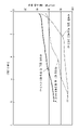
도 6은 실시예 1에 있어서, 발명예 및 비교예의 반도체 장치의, 도전성 열전도 부재의 저항값을 바꾼 경우의, 주파수에 따른 전계 강도를 나타내는 그래프이다.
도 7은 실시예 2에 있어서, 반도체 장치의 도전성 열전도 부재의 자기 특성을 바꾼 경우의, 주파수에 따른 전계 강도를 나타내는 그래프이다. 한 도면이다.
도 8의 (a)는, 종래의 반도체 장치의 일 실시 형태에 대하여, 단면의 상태를 모식적으로 도시한 도면이며, (b)는, 종래의 반도체 장치의 다른 실시 형태에 대하여, 단면의 상태를 모식적으로 도시한 도면이다.BRIEF DESCRIPTION OF THE DRAWINGS It is a figure which shows typically the state of the cross section about one Embodiment of the semiconductor device of this invention.
2 is a diagram schematically showing a state of a cross section of another embodiment of the semiconductor device of the present invention.
3 is a diagram schematically showing a state of a cross section of another embodiment of the semiconductor device of the present invention.
4 is a perspective view schematically showing an assembled state of an embodiment of the semiconductor device of the present invention.
Fig. 5 is a diagram schematically showing a model of a semiconductor device used for analysis of frequency characteristics in Examples, (a) is a state seen from the front side of the model of the semiconductor device, (b) is a model of the semiconductor device shows the state seen from the back side of
Fig. 6 is a graph showing the electric field strength according to the frequency in the case of changing the resistance value of the conductive heat-conducting member of the semiconductor device of the invention example and the comparative example in Example 1;
Fig. 7 is a graph showing the electric field strength according to the frequency when the magnetic properties of the conductive heat-conducting member of the semiconductor device are changed in Example 2; it is one drawing
Fig. 8(a) is a diagram schematically showing a state of a cross section of a conventional semiconductor device according to an embodiment, and (b) is a state of a cross section of another embodiment of a conventional semiconductor device. is a diagram schematically showing
이하, 본 발명의 실시 형태의 일례를, 도면을 사용하여 구체적으로 설명한다.EMBODIMENT OF THE INVENTION Hereinafter, an example of embodiment of this invention is concretely demonstrated using drawings.
여기서, 도 1 내지 3은, 본 발명의 반도체 장치의 실시 형태에 대하여, 단면을 모식적으로 도시한 도면이다. 또한, 도 4는, 본 발명의 반도체 장치의 일 실시 형태에 대하여, 조립 상태를 설명하기 위한 사시도이다. 또한, 각 도면에 대해서는, 설명의 편의를 위해, 각 부재의 형상이나 스케일이 실제의 것과는 상이한 상태로 나타나 있다. 각 부재의 형상이나 스케일에 대해서는, 본 명세서 중에서 규정되어 있는 것 이외에는, 반도체 장치마다 적절히 변경하는 것이 가능하다.1 to 3 are diagrams schematically showing a cross section of an embodiment of the semiconductor device of the present invention. 4 is a perspective view for explaining an assembled state of an embodiment of the semiconductor device of the present invention. In addition, about each figure, for the convenience of description, the shape and scale of each member are shown in the state different from an actual thing. About the shape and scale of each member, it is possible to change suitably for every semiconductor device except what is prescribed|regulated in this specification.
<반도체 장치><Semiconductor device>
본 발명의 반도체 장치(1)는, 도 1 내지 3에 나타내는 바와 같이, 반도체 소자(30)와, 상기 반도체 소자(30)의 상부에 마련된 도전성의 냉각 부재(40)와, 상기 반도체 장치(30)와 상기 냉각 부재(40) 사이에 마련된, 수지의 경화물을 함유하는 도전성 열전도 부재(10)를 구비한다.1 to 3 , a
그리고, 본 발명의 반도체 장치(1)에서는, 도 1 내지 3에 나타내는 바와 같이, 상기 기판(50) 중의 그라운드(60)에 접속하고, 상기 냉각 부재(40)와 상기 그라운드(60)를 전기적으로 접속하고 있는 것을 특징으로 한다.Then, in the
상기 반도체 소자(30)는, 열 및 전자파의 발생원이 되지만, 도전성을 갖고, 또한 열전도성이 높은 시트 부재(도전성 열전도 부재(10))를 반도체 소자(30)와 냉각 부재(40) 사이에 마련함으로써, 냉각 부재(40)로의 열전도가 개선되는 결과, 우수한 방열성을 실현할 수 있다.The
또한, 본 발명의 반도체 장치(1)는, 수지의 경화물을 함유하고, 도 1 내지 3에 나타내는 바와 같이, 상기 기판(50) 중의 그라운드(60)와 접속함으로써, 상기 냉각 부재(40)와 상기 그라운드(60)가, 상기 도전성 열전도 부재(10)를 통하여 전기적으로 접속하고, 본 발명의 반도체 장치(1) 내에 있어서 전기적으로 닫힌 공간(도 1 내지 3의 파선으로 둘러싼 공간)이 형성되는 결과, 전자파 차단 효과를 높이는 것이 가능해지고, 우수한 전자파 억제 효과도 실현할 수 있다.In addition, the
또한, 본 발명의 반도체 장치(1)에서는, 실드 캔 등의 전자파 실드 부재가 별도 형성되어 있지 않기 때문에, 종래의 전자파 실드 부재를 사용한 기술에 비하여, 제조 비용의 저감 및 제조의 용이성 향상을 도모해도 된다.Further, in the
또한, 도 8의 (a) 및 (b)는, 종래 기술에 의한 반도체 장치의 예를 나타낸 것이다. 도 8의 (a)에 도시된 반도체 장치(100)에서는, 반도체 소자(30)를 덮도록 도전성 열전도 부재(10)를 마련하고 있기 때문에, 높은 방열 효과가 얻어진다. 그러나, 도전성 열전도 부재(10)와 그라운드(60)의 접속이 없기 때문에, 반도체 장치(1) 내에 있어서 전기적으로 닫힌 공간을 형성할 수 없고, 충분한 전자파 억제 효과를 얻을 수 없다.8A and 8B show examples of a semiconductor device according to the prior art. In the
또한, 도 8의 (b)에 도시된 반도체 장치(100)에서는, 도전성 열전도 부재(10)가 실드 캔(20)을 통하여 적층되는 구성인 점에서, 본 발명의 반도체 장치(1)에 비하여, 반도체 소자(30)와 냉각 부재(40) 사이의 열저항이 크고, 충분한 방열성을 얻을 수 없다.In addition, in the
다음에, 본 발명의 반도체 장치를 구성하는 각 부재에 대해서 설명한다.Next, each member constituting the semiconductor device of the present invention will be described.
(반도체 소자)(Semiconductor device)
본 발명의 반도체 장치(1)는, 도 1 내지 3에 나타내는 바와 같이, 기판(50) 상에 형성된 반도체 소자(30)를 구비한다.The
여기서, 상기 반도체 소자에 대해서는, 반도체에 의한 전자 부품이면 특별히 한정되는 것이 아니다. 예를 들어, IC나 LSI 등의 집적 회로, CPU, MPU, 그래픽 연산 소자, 이미지 센서 등을 들 수 있다.Here, about the said semiconductor element, if it is an electronic component by a semiconductor, it will not specifically limit. For example, integrated circuits, such as IC and LSI, CPU, MPU, a graphic computing element, an image sensor, etc. are mentioned.
상기 반도체 소자(30)가 형성되는 기판(50)에 대해서는, 상기 그라운드(GND)(60)가 마련되어 있는 것 이외는 특별히 한정은 되지 않고, 반도체 장치의 종류에 따라, 적합한 것을 사용할 수 있다. 그라운드(60)는, 이면측에 형성된다.The
또한, 도 1 및 도 2에서는, 상기 도전성 열전도 부재(10)가, 상기 기판(50) 상에 노출된 그라운드(60)와 직접 접속하는 구성으로 되어 있지만, 본 발명의 반도체 장치(1)에서는, 예를 들어 도 3에 나타내는 바와 같이, 상기 기판(50)의 면 상에, 상기 반도체 소자(30)의 주위를 둘러싸도록, 전체 둘레 또는 부분적으로 랜드(51)를 마련해도 된다. 이 랜드(51)와 상기 도전성 열전도 부재(10)를 접속시킴으로써, 상기 그라운드(60)의 전기적인 접속이 가능해진다. 상기 랜드(51)는, 상기 기판(50)에 중에 형성된 도전 처리 스루홀(52)을 통하여 상기 그라운드(60)와 전기적으로 접속되어 있고, 이에 의해 상기 도전 실드 캔(20)을 그라운드(60)와 전기적으로 접합시킬 수 있다.1 and 2, the conductive heat-conducting
또한, 상기 기판(50)에 대해서는, 상기 그라운드 이외의 부분이, 절연 처리되어 있는 것이 바람직하다. 상기 도전성 열전도 부재(10)가 타부품에 접촉해 버리면 단락하고, 고장의 원인이 되기 때문에, 타부품의 보호를 도모하기 위해, 그라운드(60)에 접속되는 부분 이외는 절연 처리되어 있는 것이 바람직하다. 따라서, 상기 기판(50)에, 랜드(51) 및 스루홀(52)이 마련되어 있는 경우에는, 이들의 부분은 절연 처리되지 않고, 도전성을 가질 필요가 있다.In addition, with respect to the
(냉각 부재)(no cooling)
본 발명의 반도체 장치(1)는, 도 1 내지 3에 나타내는 바와 같이, 상기 반도체 소자(30)의 상부에 마련된, 도전성의 냉각 부재(40)를 구비한다.The
여기서, 상기 냉각 부재(40)는, 상기 열원(반도체 소자(30))으로부터 발생되는 열을 흡수하고, 외부로 방산시키는 부재이다. 후술하는 도전성 열전도 부재(10)를 통하여 상기 반도체 소자(30)와 접속됨으로써, 반도체 소자(30)가 발생한 열을 외부에 확산시키고, 반도체 장치가 높은 방열성을 실현할 수 있다.Here, the cooling
또한, 상기 냉각 부재(40)는 도전성을 갖기 때문에, 후술하는 도전성 열전도 부재(10)를 통하여, 상기 그라운드(60)와 전기적으로 접속됨으로써, 전기적으로 닫힌 공간(도 1 내지 3의 파선으로 둘러싼 영역 A)을 형성하고, 반도체 장치(1)의 전자파 억제 효과를 높일 수 있다.In addition, since the cooling
상기 도전 냉각 부재(40)의 종류에 대해서는, 특별히 한정은 되지 않고, 본 발명의 반도체 장치(1)의 종류에 따라 적절히 선택할 수 있다. 예를 들어, 방열기, 냉각기, 히트 싱크, 히트 스프레더, 다이 패드, 냉각 팬, 히트 파이프, 금속 커버, 하우징 등을 들 수 있다. 이들 도전 냉각 부재 중에서도 보다 우수한 방열성이 얻어지는 점에서는, 도전성을 갖는 방열기, 냉각기 또는 히트 싱크를 사용하는 것이 바람직하다. 또한, 상술한 도전 냉각 부재(40)를 구성하는 재료에 대해서는, 열전도율을 높이는 점에서, 알루미늄, 구리, 스테인리스 등의 금속이나, 그래파이트 등을 포함하는 것이 바람직하다.The type of the
(도전성 열전도 부재)(No conductive heat conduction)
본 발명의 반도체 장치(1)는, 도 1 내지 3에 나타내는 바와 같이, 상기 반도체 소자(30)와, 상기 도전 냉각 부재(40) 사이에 마련된, 수지의 경화물을 함유하는 도전성 열전도 부재(10)를 구비하고, 상기 도전성 열전도 부재(10)가, 상기 기판(50) 중의 그라운드(60)에 접속하고, 상기 냉각 부재(40)와 상기 그라운드(60)가, 도전성 열전도 부재(10)를 통하여 전기적으로 접속하고 있는 것을 특징으로 한다.1 to 3, the
열전도성이 높은 도전성 열전도 부재(10)가, 반도체 소자(30)와 냉각 부재(40) 사이에 마련됨으로써, 전자파 억제 효과를 저하시키지 않고, 방열성에 대해서도 향상시키는 것이 가능해진다. 그 외에도, 도전성을 갖는 상기 도전성 열전도 부재(10)를 통하여, 상기 냉각 부재(40)와 상기 그라운드(60)가 전기적으로 접속함으로써, 도 1 내지 3에 나타내는 바와 같이, 본 발명의 반도체 장치(1) 내에 있어서 전기적으로 닫힌 공간 A가 형성되는 결과, 도전 실드 캔(20)의 전자파 차단 효과를 높이는 것이 가능해지고, 우수한 전자파 억제 효과를 실현할 수 있다.By providing the conductive heat-conducting
여기서, 상기 도전성 열전도 부재(10) 형상에 대해서는, 특별히 한정은 되지 않고, 상기 반도체 소자(30)의 형상이나 크기, 반도체 장치(1)의 설계 내용 등에 따라, 적절히 변경할 수 있다.Here, the shape of the conductive heat
구체적으로는, 도 1 및 도 3에 나타내는 바와 같이, 상기 반도체 장치(30)와 상기 냉각 부재(40) 사이에 마련되어 있는 절곡된 시트와 같은 상태로 마련할 수 있다. 상기 도전성 열전도 부재(10)는, 수지의 경화물을 함유하고, 유연성이 어느 정도 있기 때문에, 번잡한 공정을 거치지 않고, 도 1 및 도 3에 나타내는 바와 같은 형상으로 하는 것이 가능하다. 또한, 도 2에 나타내는 바와 같이, 상기 반도체 장치(30)의 주위를 모두 둘러싸도록(상기 반도체 소자(30)의 상면(30b) 및 측면(30a)을 밀봉함) 마련해도 된다.Specifically, as shown in FIGS. 1 and 3 , it can be provided in the same state as a bent sheet provided between the
또한, 보다 우수한 전자파 억제 효과를 실현하는 관점에서는, 도 1 및 도 2에 나타내는 바와 같이, 상기 도전성 열전도 부재(10)가, 상기 반도체 소자(30)를 덮도록 마련되어, 상기 반도체 소자(30)의 상면(30b) 및 측면(30a)의 적어도 일부와, 맞닿아 있는 것이 바람직하다. 상기 냉각 부재(40)와 상기 그라운드(60)의 전기적인 접속을 효율적으로 확보할 수 있기 때문에, 보다 확실하게 전기적으로 닫힌 공간 A를 형성할 수 있다.In addition, from the viewpoint of realizing a more excellent electromagnetic wave suppression effect, as shown in FIGS. 1 and 2 , the conductive heat-conducting
또한, 마찬가지의 관점에서, 상기 도전성 열전도 부재(10)가, 도 2에 나타내는 바와 같이, 상기 반도체 소자(30)의 상면(30b) 및 측면(30a)을, 밀봉하고 있는 것이 보다 바람직하다.In addition, from the same viewpoint, it is more preferable that the conductive heat
또한, 상기 도전성 열전도 부재(10)는, 1층의 시트로 구성해도 되고, 복수매의 시트로 구성할 수도 있다.In addition, the said electroconductive heat
예를 들어, 도 1 및 도 3에 나타내는 바와 같이, 상기 도전성 열전도 부재(10)가 절곡된 시트와 같이 마련되는 경우에는, 상기 도전성 열전도 부재(10)를 1층의 시트에 의해 구성할 수 있다. 단, 시트의 두께를 조정하기 쉽다는 등의 관점에서, 복수의 시트로 구성할 수도 있다.For example, as shown in FIGS. 1 and 3 , when the conductive heat-conducting
또한, 도 2에 나타내는 바와 같이, 상기 도전성 열전도 부재(10)가, 상기 반도체 소자(30)의 상면(30b) 및 측면(30a)을 밀봉하고 있는 경우에는, 1매의 상기 도전성 열전도 부재(10)를 가공할 수도 있고, 복수의 상기 도전성 열전도 부재(10)를 조합함으로써 상기 도전성 열전도 부재(10)를 구성할 수도 있다.In addition, as shown in FIG. 2, when the said conductive heat-conducting
또한, 상기 도전성 열전도 부재(10)의 두께 T에 대해서는, 특별히 한정은 되지 않고, 반도체 소자(30)와 냉각 부재(40)의 거리나, 반도체 장치(1)의 설계 내용 등에 따라 적절히 변경할 수 있다. 단, 방열성 및 전자파 억제 효과를 보다 높은 레벨로 실현할 수 있다는 점에서는, 상기 도전성 열전도 부재(10)의 두께 T가 50㎛ 내지 4㎜인 것이 바람직하고, 100㎛ 내지 4㎜인 것이 보다 바람직하고, 200㎛ 내지 3㎜인 것이 특히 바람직하다. 상기 도전성 열전도 부재(10)의 두께 T가 4㎜를 초과하면, 상기 반도체 소자(30)와 상기 냉각 부재(40)의 거리가 길어지기 때문에, 열전도성이 저하될 우려가 있고, 한편, 상기 도전성 열전도 부재(10)의 두께 T가 50㎛ 미만인 경우에는, 전자파 억제 효과가 작아질 우려가 있다.In addition, the thickness T of the said conductive heat-conducting
여기서, 상기 도전성 열전도 부재(10)의 두께 T는, 도 1 내지 3에 나타내는 바와 같이, 상기 반도체 소자(30) 상의 상기 도전성 열전도 부재(10) 중 가장 두께가 큰 부분의 두께 T를 의미하고, 1층의 시트로부터 형성되는지나, 복수의 시트로부터 형성되는지는 상관없다.Here, the thickness T of the conductive heat-conducting
상기 도전성 열전도 부재(10)는, 수지의 경화물을 함유하는 것을 요한다. 수지의 경화물을 함유함으로써, 상기 도전성 열전도 부재(10)가 어느 정도의 유연성을 가질 수 있어, 제조의 용이성을 높일 수 있다.The conductive heat
또한, 상기 도전성 열전도 부재(10)의 유연성에 대해서는, 높을수록 바람직하고, 구체적으로는 고무 경도 쇼어 OO(ASTM D2240)가 10 내지 80의 범위가 되는 것이 바람직하다.In addition, the flexibility of the conductive heat
또한, 상기 도전성 열전도 부재(10)에 대해서는, 우수한 전자파 억제 효과를 실현하는 점에서는, 도전성이 높은 것이 바람직하다.Moreover, about the said electroconductive heat-conducting
구체적으로는, 상기 도전성 열전도 부재(10)의 저항률이, 0.15Ωㆍm 이하인 것이 바람직하고, 0.01Ωㆍm 이하인 것이 보다 바람직하고, 0.005Ωㆍm 이하인 것이 더욱 바람직하고, 0.001Ωㆍm 이하인 것이 특히 바람직하다. 상기 도전성 부재(11)의 저항률을 0.15Ωㆍm 이하로 함으로써, 보다 우수한 전자파 억제 효과가 얻어지기 때문이다.Specifically, the resistivity of the conductive heat
또한, 상기 도전성 열전도 부재(10)의 저항률에 대해서는, 0.00001Ωㆍm 이상인 것이 바람직하다. 저항률이 낮은, 즉 도전율이 클수록 전자파 차폐 성능은 커지고, 전자파 억제 효과를 높일 수 있다.Moreover, about the resistivity of the said conductive heat-conducting
또한, 상기 도전성 열전도 부재(10)의 도전성(저항률)의 조정 방법으로는, 특별히 한정은 되지 않지만, 결합제 수지의 종류나, 충전제의 재료, 배합량 및 배향 방향 등을 바꿈으로써, 조정하는 것이 가능하다.The method for adjusting the conductivity (resistivity) of the conductive heat
또한, 상기 도전성 열전도 부재(10)는, 5W/mK 이상인 것이 바람직하고, 10W/mK 이상인 것이 보다 바람직하고, 20W/mK 이상인 것이 특히 바람직하다. 반도체 소자(30)와 냉각 부재(40) 사이의 열 교환 효율을 보다 높일 수 있고, 방열성을 더 향상시킬 수 있기 때문이다.Further, the conductive heat
또한, 상기 도전성 열전도 부재(10)는, 자기 특성을 갖는 것이 바람직하다. 상기 도전성 열전도 부재(10)에, 전자파 흡수 성능을 갖게 할 수 있기 때문에, 더 우수한 전자파 억제 효과가 얻어지기 때문이다.In addition, the conductive heat
여기서, 상기 도전성 열전도 부재(10)의 자기 특성의 조정 방법으로는, 특별히 한정은 되지 않지만, 도전성 열전도 부재(10) 중에, 자성분 등을 함유시키고, 그의 배합량 등을 바꿈으로써, 조정하는 것이 가능하다.Here, the method for adjusting the magnetic properties of the conductive heat
또한, 상기 도전성 열전도 부재(10)는, 표면에 점착성 또는 접착성을 갖는 것이 바람직하다. 도전성 열전도 부재(10)와 다른 부재의 접착성을 향상시킬 수 있기 때문이다. 또한, 상기 도전성 열전도 부재(10)가 복수의 시트로 구성되는 경우에는, 시트끼리의 접착성에 대해서도 향상시킬 수 있다.Moreover, it is preferable that the said conductive heat-conducting
또한, 상기 도전성 열전도 부재(10)의 표면에 태크성을 부여하는 방법에 대해서는 특별히 한정은 되지 않는다. 예를 들어, 후술하는 도전성 열전도 부재(10)를 구성하는 결합제 수지의 적정화를 도모하여 태크성을 갖게 할 수도 있고, 상기 도전성 열전도 부재(10)의 표면에 태크성이 있는 접착층을 별도 마련해도 된다.In addition, limitation in particular is not carried out about the method of providing tackiness to the surface of the said conductive heat-conducting
또한, 상기 도전성 열전도 부재(10)를 구성하는 재료에 대해서는, 우수한 전자파 흡수 성능 및 열전도성을 갖는 것이면 특별히 한정은 되지 않는다.In addition, about the material which comprises the said electroconductive heat-conducting
예를 들어, 높은 레벨로, 전자파 흡수 성능 및 열전도성을 실현할 수 있다는 점에서는, 상기 도전성 열전도 부재가, 결합제 수지와, 도전성을 갖는 열전도성 충전제와, 그밖의 성분을 포함할 수 있다.For example, in terms of realizing electromagnetic wave absorption performance and thermal conductivity at a high level, the conductive heat conductive member may include a binder resin, a conductive thermally conductive filler, and other components.
이하, 도전성 열전도 부재(10)를 구성하는 재료에 대하여 기재한다.Hereinafter, the material constituting the conductive heat
ㆍ결합제 수지ㆍBinder resin
상기 도전성 열전도 부재를 구성하는 결합제 수지란, 도전성 열전도 부재의 기재가 되는 수지 성분의 경화물이다. 그 종류에 대해서는, 특별히 한정되지 않고 공지된 결합제 수지를 적절히 선택할 수 있다. 예를 들어, 결합제 수지의 하나로서, 열경화성 수지를 들 수 있다.The binder resin constituting the conductive heat conductive member is a cured product of a resin component serving as a base material of the conductive heat conductive member. It does not specifically limit about the kind, A well-known binder resin can be selected suitably. For example, as one of binder resins, a thermosetting resin is mentioned.
상기 열경화성 수지로서는, 예를 들어 가교성 고무, 에폭시 수지, 폴리이미드 수지, 비스말레이미드 수지, 벤조시클로부텐 수지, 페놀 수지, 불포화 폴리에스테르, 디알릴프탈레이트 수지, 실리콘, 폴리우레탄, 폴리이미드 실리콘, 열경화형 폴리페닐렌에테르, 열경화형 변성 폴리페닐렌에테르 등을 들 수 있다. 이들은, 1종 단독으로 사용해도 되고, 2종 이상을 병용해도 된다.Examples of the thermosetting resin include crosslinkable rubber, epoxy resin, polyimide resin, bismaleimide resin, benzocyclobutene resin, phenol resin, unsaturated polyester, diallyl phthalate resin, silicone, polyurethane, polyimide silicone, Thermosetting polyphenylene ether, thermosetting modified polyphenylene ether, etc. are mentioned. These may be used individually by 1 type, and may use 2 or more types together.
또한, 상기 가교성 고무로서는, 예를 들어 천연 고무, 부타디엔 고무, 이소프렌 고무, 니트릴 고무, 수소 첨가 니트릴 고무, 클로로프렌 고무, 에틸렌프로필렌 고무, 염소화 폴리에틸렌, 클로로술폰화 폴리에틸렌, 부틸 고무, 할로겐화 부틸 고무, 불소 고무, 우레탄 고무, 아크릴 고무, 폴리이소부틸렌 고무, 실리콘 고무 등을 들 수 있다. 이들은, 1종 단독으로 사용해도 되고, 2종 이상을 병용해도 된다.Examples of the crosslinkable rubber include natural rubber, butadiene rubber, isoprene rubber, nitrile rubber, hydrogenated nitrile rubber, chloroprene rubber, ethylene propylene rubber, chlorinated polyethylene, chlorosulfonated polyethylene, butyl rubber, halogenated butyl rubber, Fluorine rubber, urethane rubber, acrylic rubber, polyisobutylene rubber, silicone rubber, etc. are mentioned. These may be used individually by 1 type, and may use 2 or more types together.
또한, 상술한 열경화성 수지 중에서도 성형 가공성 및 내후성이 우수함과 함께, 전자 부품에 대한 밀착성 및 추종성의 관점에서, 실리콘을 사용하는 것이 바람직하다. 실리콘으로서는, 특별히 제한은 없고, 목적에 따라 실리콘의 종류를 적절히 선택할 수 있다.Moreover, while it is excellent in moldability and weather resistance among the thermosetting resins mentioned above, it is preferable to use silicone from a viewpoint of the adhesiveness with respect to an electronic component and followability|trackability. There is no restriction|limiting in particular as silicone, The kind of silicone can be selected suitably according to the objective.
상술한 성형 가공성, 내후성, 밀착성 등을 얻는 관점에서는, 상기 실리콘으로서, 액상 실리콘 겔의 주제와, 경화제로부터 구성되는 실리콘인 것이 바람직하다. 그러한 실리콘으로서는, 예를 들어 부가 반응형 액상 실리콘, 과산화물을 가황에 사용하는 열 가황형 밀러블 타입의 실리콘 등을 들 수 있다.From the viewpoint of obtaining the above-described moldability, weather resistance, adhesiveness, and the like, the silicone is preferably a silicone composed of a main component of a liquid silicone gel and a curing agent. As such silicone, for example, addition reaction type liquid silicone, heat vulcanization type millable type silicone using peroxide for vulcanization, etc. are mentioned.
상기 부가 반응형 액상 실리콘으로서는, 비닐기를 갖는 폴리오르가노실록산을 주제, Si-H기를 갖는 폴리오르가노실록산을 경화제로 한, 2액성의 부가 반응형 실리콘 등을 사용하는 것이 바람직하다.As said addition-reaction liquid silicone, it is preferable to use the two-component addition-reaction type silicone etc. which used the polyorganosiloxane which has a vinyl group as a main agent and the polyorganosiloxane which has Si-H group as a hardening|curing agent.
또한, 상기 액상 실리콘 겔의 주제와, 경화제와의 조합에 있어서, 상기 주제와 상기 경화제와의 배합 비율로서는, 질량비로, 주제:경화제=35:65 내지 65:35인 것이 바람직하다.Further, in the combination of the main agent and the curing agent of the liquid silicone gel, the mixing ratio of the main agent and the curing agent is preferably, in a mass ratio, the main agent:curing agent = 35:65 to 65:35.
또한, 상기 도전성 열전도 부재에 있어서의 상기 결합제 수지의 함유량은, 특별히 제한되지 않으며, 목적에 따라 적절히 선택할 수 있다. 예를 들어, 시트의 성형 가공성이나, 시트의 밀착성 등을 확보하는 관점에서는, 상기 도전성 열전도 부재의 20체적% 내지 50체적% 정도인 것이 바람직하고, 30체적% 내지 40체적%인 것이 보다 바람직하다.In addition, content in particular of the said binder resin in the said electroconductive heat conductive member is not restrict|limited, According to the objective, it can select suitably. For example, from the viewpoint of ensuring the formability of the sheet and the adhesiveness of the sheet, it is preferably about 20 to 50% by volume, and more preferably 30 to 40% by volume of the conductive heat conductive member. .
ㆍ도전성을 갖는 열전도성 충전제ㆍThermal conductive filler with conductivity
도전성 열전도 부재는, 상기 결합제 수지 내에, 도전성을 갖는 열전도성 충전제(이하, 간단히 「열전도성 충전제」라고 하는 경우도 있음)를 포함한다. 상기 도전성을 갖는 열전도성 충전제는, 시트의 열전도성 및 도전성을 향상시키기 위한 성분이다.The conductive heat conductive member contains a conductive heat conductive filler (hereinafter, simply referred to as "thermal conductive filler" in some cases) in the binder resin. The thermally conductive filler which has the said electroconductivity is a component for improving the thermal conductivity and electroconductivity of a sheet|seat.
여기서, 열전도성 충전제의 종류에 대해서는, 특별히 한정은 되지 않지만, 더 높은 열전도성을 실현할 수 있다는 점에서는, 섬유상의 열전도성 충전제를 사용하는 것이 바람직하다.Here, the kind of the thermally conductive filler is not particularly limited, but it is preferable to use a fibrous thermally conductive filler from the viewpoint of realizing higher thermal conductivity.
또한, 상기 섬유상의 열전도성 충전제의 「섬유상」이란, 애스펙트비가 높은(약 6 이상)의 형상을 말한다. 그 때문에, 본 발명에서는, 섬유상이나 봉상 등의 열전도성 충전제뿐만 아니라, 애스펙트비가 높은 입자 형상의 충전재나, 플레이크상의 열전도성 충전제 등도 섬유상의 열전도성 충전제에 포함된다.In addition, the "fibrous form" of the said fibrous thermal conductive filler means the shape with a high aspect-ratio (about 6 or more). Therefore, in the present invention, not only fibrous and rod-shaped thermally conductive fillers, but also particulate fillers with high aspect ratios, flaky thermally conductive fillers, and the like are included in the fibrous thermally conductive fillers.
여기서, 상기 섬유상의 열전도성 충전제의 종류에 대해서는, 섬유상이면서 또한 열전도성 및 도전성이 높은 재료이면 특별히 한정은 되지 않고, 예를 들어 은, 구리, 알루미늄 등의 금속, 알루미나, 질화알루미늄, 탄화규소, 그래파이트 등의 세라믹스, 탄소 섬유 등을 들 수 있다.Here, the type of the fibrous thermally conductive filler is not particularly limited as long as it is a fibrous material with high thermal conductivity and conductivity, for example, metals such as silver, copper, aluminum, alumina, aluminum nitride, silicon carbide, Ceramics, such as graphite, carbon fiber, etc. are mentioned.
이들 섬유상의 열전도성 충전제 중에서도 더 높은 열전도성 및 도전성이 얻어지는 점에서는, 탄소 섬유를 사용하는 것이 보다 바람직하다.Among these fibrous thermally conductive fillers, it is more preferable to use carbon fibers from the viewpoint of obtaining higher thermal conductivity and conductivity.
또한, 상기 도전성을 갖는 열전도성 충전제에 대해서는, 1종 단독이어도 되고, 2종 이상을 혼합하여 사용할 수도 있다. 또한, 2종 이상의 열전도성 충전제를 사용하는 경우에는, 모두 섬유상의 열전도성 충전제여도 되고, 섬유상의 열전도성 충전제와 다른 형상의 열전도성 충전제를 혼합하여 사용할 수도 있다.In addition, about the said electroconductive thermal conductive filler which has electroconductivity, 1 type may be used alone, or 2 or more types may be mixed and used for it. In addition, when two or more types of thermally conductive fillers are used, all may be a fibrous thermally conductive filler, and a fibrous thermally conductive filler and the thermally conductive filler of a different shape may be mixed and used.
상기 탄소 섬유의 종류에 대하여 특별히 제한은 없고, 목적에 따라 적절히 선택할 수 있다. 예를 들어, 피치계, PAN계, PBO 섬유를 흑연화한 것, 아크 방전법, 레이저 증발법, CVD법(화학 기상 성장법), CCVD법(촉매 화학 기상 성장법) 등으로 합성된 것을 사용할 수 있다. 이들 중에서도 높은 열전도성 및 도전성이 얻어진다는 점에서, PBO 섬유를 흑연화한 탄소 섬유, 피치계 탄소 섬유가 보다 바람직하다.There is no restriction|limiting in particular about the kind of said carbon fiber, According to the objective, it can select suitably. For example, pitch-based, PAN-based, graphitized PBO fibers, arc discharge method, laser evaporation method, CVD method (chemical vapor deposition method), CCVD method (catalytic chemical vapor deposition method), etc. can be used can Among these, carbon fibers obtained by graphitizing PBO fibers and pitch-based carbon fibers are more preferred from the viewpoint that high thermal conductivity and conductivity are obtained.
또한, 상기 탄소 섬유는, 필요에 따라, 그의 일부 또는 전부를 표면 처리하여 사용할 수 있다. 상기 표면 처리로서는, 예를 들어 산화 처리, 질화 처리, 니트로화, 술폰화, 또는 이들 처리에 의해 표면에 도입된 관능기 혹은 탄소 섬유의 표면에, 금속, 금속 화합물, 유기 화합물 등을 부착 또는 결합시키는 처리 등을 들 수 있다. 상기 관능기로서는, 예를 들어 수산기, 카르복실기, 카르보닐기, 니트로기, 아미노기 등을 들 수 있다.In addition, if necessary, the carbon fiber may be used by surface-treating a part or all of it. As the surface treatment, for example, oxidation treatment, nitriding treatment, nitration, sulfonation, or attaching or bonding a metal, a metal compound, an organic compound, etc. to the surface of a functional group or carbon fiber introduced into the surface by these treatments treatment and the like. As said functional group, a hydroxyl group, a carboxyl group, a carbonyl group, a nitro group, an amino group, etc. are mentioned, for example.
또한, 상기 섬유상의 열전도성 충전제의 평균 섬유 길이(평균 장축 길이)에 대해서도, 특별히 제한은 없게 적절히 선택할 수 있지만, 확실하게 높은 열전도성을 얻는 점에서, 50㎛ 내지 300㎛의 범위인 것이 바람직하고, 75㎛ 내지 275㎛의 범위인 것이 보다 바람직하고, 90㎛ 내지 250㎛의 범위인 것이 특히 바람직하다.Also, the average fiber length (average major axis length) of the fibrous thermally conductive filler is not particularly limited and can be appropriately selected, but it is preferably in the range of 50 µm to 300 µm from the viewpoint of reliably obtaining high thermal conductivity, , more preferably in the range of 75 µm to 275 µm, particularly preferably in the range of 90 µm to 250 µm.
또한, 상기 섬유상의 열전도성 충전제의 평균 섬유 직경(평균 단축 길이)에 대해서도, 특별히 제한은 없게 적절히 선택할 수 있지만, 확실하게 높은 열전도성을 얻는 점에서, 4㎛ 내지 20㎛의 범위인 것이 바람직하고, 5㎛ 내지 14㎛의 범위인 것이 보다 바람직하다.Also, the average fiber diameter (average minor axis length) of the fibrous thermally conductive filler is not particularly limited and can be appropriately selected, but it is preferably in the range of 4 µm to 20 µm from the viewpoint of reliably obtaining high thermal conductivity, , more preferably in the range of 5 µm to 14 µm.
상기 섬유상의 열전도성 충전제의 애스펙트비(평균 장축 길이/평균 단축 길이)에 대해서는, 확실하게 높은 열전도성을 얻는 점에서, 6 이상인 것이 사용되고, 7 내지 30인 것이 바람직하다. 상기 애스펙트비가 작은 경우에서도 열전도율 등의 개선 효과는 보여지지만, 배향성이 저하되는 등에 의해 큰 특성 개선 효과가 얻어지지 않기 때문에, 애스펙트비는 6 이상으로 한다. 한편, 30을 초과하면, 도전성 열전도 부재 중에서의 분산성이 저하되기 때문에, 충분한 열전도율을 얻지 못할 우려가 있다.About the aspect-ratio (average long-axis length/average minor-axis length) of the said fibrous thermally conductive filler, from a point which reliably acquires high thermal conductivity, a thing of 6 or more is used, and it is preferable that it is 7-30. Even when the aspect ratio is small, an improvement effect such as thermal conductivity is observed, but since a large characteristic improvement effect is not obtained due to a decrease in orientation or the like, the aspect ratio is set to 6 or more. On the other hand, when it exceeds 30, since the dispersibility in an electroconductive heat-conducting member falls, there exists a possibility that sufficient thermal conductivity may not be obtained.
여기서, 상기 섬유상의 열전도성 충전제의 평균 장축 길이 및 평균 단축 길이는, 예를 들어 마이크로스코프, 주사형 전자 현미경(SEM) 등에 의해 측정하고, 복수의 샘플로부터 평균을 산출할 수 있다.Here, the average major axis length and the average minor axis length of the fibrous thermally conductive filler can be measured with, for example, a microscope, a scanning electron microscope (SEM), or the like, and an average can be calculated from a plurality of samples.
또한, 상기 도전성 열전도 부재에 있어서의, 상기 도전성을 갖는 열전도성 충전제의 함유량으로서는, 특별히 제한은 없고, 목적에 따라 적절히 선택할 수 있지만, 4체적% 내지 40체적%인 것이 바람직하고, 5체적% 내지 30체적%인 것이 보다 바람직하고, 6체적% 내지 20체적%인 것이 특히 바람직하다. 상기 함유량이 4체적% 미만이면, 충분히 낮은 열저항을 얻기가 곤란해질 우려가 있고, 40체적%를 초과하면, 상기 도전성 열전도 부재의 성형성 및 상기 섬유상의 열전도성 충전제의 배향성에 영향을 주게 되어 버릴 우려가 있다.Moreover, there is no restriction|limiting in particular as content of the heat conductive filler which has the said electroconductivity in the said electroconductive heat conductive member, According to the objective, although it can select suitably, It is preferable that it is 4 volume% - 40 volume%, and 5 volume% - It is more preferable that it is 30 volume%, and it is especially preferable that it is 6 volume% - 20 volume%. When the content is less than 4% by volume, there is a fear that it may be difficult to obtain a sufficiently low thermal resistance, and when it exceeds 40% by volume, the moldability of the conductive heat-conducting member and the orientation of the fibrous thermally conductive filler are affected there is a risk of throwing it away.
또한, 상기 도전성 열전도 부재에서는, 상기 도전성을 갖는 열전도성 충전제가 한 방향 또는 복수의 방향으로 배향되어 있는 것이 바람직하다. 상기 열전도성 충전제를 배향시킴으로써 보다 높은 열전도성이나 전자파 흡수성을 실현할 수 있기 때문이다.Moreover, in the said electroconductive heat conductive member, it is preferable that the heat conductive filler which has the said electroconductivity is oriented in one direction or a plurality of directions. It is because higher thermal conductivity and electromagnetic wave absorptivity can be implement|achieved by orientating the said thermally conductive filler.
예를 들어, 상기 도전성 열전도 부재에 의한 열전도성 및 도전성을 높이고, 본 발명의 반도체 장치의 방열성 및 을 향상시키고자 하는 경우에는, 상기 열전도성 충전제를 시트면에 대하여 대략 수직형으로 배향시킬 수 있다. 한편, 상기 도전성 열전도 부재 중의 전기의 흐름을 바꿀 경우 등에는, 상기 열전도성 충전제를 시트면에 대하여 대략 평행형이나 그 밖의 방향으로 배향시킬 수 있다.For example, when it is desired to increase the thermal conductivity and conductivity by the conductive heat-conducting member, and to improve the heat dissipation properties of the semiconductor device of the present invention, the thermally conductive filler may be oriented substantially perpendicular to the sheet surface. . On the other hand, in the case of changing the flow of electricity in the conductive heat conductive member, the heat conductive filler can be oriented in a substantially parallel shape or other direction with respect to the sheet surface.
여기서, 상기 시트면에 대하여 대략 수직형이나, 대략 평행의 방향은, 상기 시트면 방향에 대하여 거의 수직인 방향이나 거의 평행한 방향을 의미한다. 단, 상기 도전성을 갖는 열전도성 충전제의 배향 방향은, 제조 시에 다소의 변동은 있기 때문에, 본 발명에서는, 상술한 시트면의 방향에 대해 수직인 방향이나 평행한 방향으로부터 ±20°정도의 어긋남은 허용된다.Here, the substantially perpendicular or substantially parallel direction to the sheet surface means a direction substantially perpendicular or substantially parallel to the sheet surface direction. However, since there is some variation in the orientation direction of the thermally conductive filler having conductivity, in the present invention, there is a deviation of about ±20° from the direction perpendicular or parallel to the direction of the sheet surface described above. is allowed
또한, 상기 도전성을 갖는 열전도성 충전제의 배향 각도를 정돈하는 방법에 대해서는, 특별히 한정은 되지 않는다. 예를 들어, 상기 도전성 열전도 부재의 바탕이 되는 시트용 성형체를 제작하고, 섬유상의 열전도성 충전제를 배향시킨 상태에서, 잘라내기 각도를 조정함으로써, 배향 각도의 조정이 가능해진다.In addition, limitation in particular is not carried out about the method of fixing the orientation angle of the thermally conductive filler which has the said electroconductivity. For example, the orientation angle can be adjusted by producing a sheet molded article serving as a base for the conductive heat conductive member, and adjusting the cut-out angle in a state in which the fibrous heat conductive filler is oriented.
ㆍ무기물 필러ㆍInorganic filler
또한, 상기 도전성 열전도 부재는, 상술한 결합제 수지 및 도전성을 갖는 열전도성 섬유에 더하여 무기물 필러를 더 포함할 수 있다. 도전성 열전도 부재의 열전도성을 더 높이거나, 시트의 강도를 향상시킬 수 있기 때문이다.In addition, the conductive heat-conducting member may further include an inorganic filler in addition to the above-described binder resin and heat-conductive fiber having conductivity. This is because the thermal conductivity of the conductive heat-conducting member can be further improved or the strength of the sheet can be improved.
상기 무기물 필러로서는, 형상, 재질, 평균 입경 등에 대해서는 특별히 제한이 되지 않고, 목적에 따라 적절히 선택할 수 있다. 상기 형상으로서는, 예를 들어 구상, 타원 구상, 괴상, 입상, 편평상, 침상 등을 들 수 있다. 이들 중에서도 구상, 타원형이 충전성의 점에서 바람직하고, 구상이 특히 바람직하다.The inorganic filler is not particularly limited in shape, material, average particle size, and the like, and may be appropriately selected according to the purpose. As said shape, a spherical shape, an elliptical spherical shape, a block shape, a granular shape, a flat shape, needle shape etc. are mentioned, for example. Among these, a spherical shape and an ellipse are preferable at the point of fillability, and a spherical shape is especially preferable.
상기 무기물 필러의 재료로서는, 예를 들어 질화알루미늄(질화알루미늄: AlN), 실리카, 알루미나(산화알루미늄), 질화붕소, 티타니아, 유리, 산화아연, 탄화규소, 규소(silicon), 산화규소, 산화알루미늄, 금속 입자 등을 들 수 있다. 이들은, 1종 단독으로 사용해도 되고, 2종 이상을 병용해도 된다. 이들 중에서도 알루미나, 질화붕소, 질화알루미늄, 산화아연, 실리카가 바람직하고, 열전도율의 관점에서, 알루미나, 질화알루미늄이 특히 바람직하다.Examples of the inorganic filler material include aluminum nitride (aluminum nitride: AlN), silica, alumina (aluminum oxide), boron nitride, titania, glass, zinc oxide, silicon carbide, silicon, silicon oxide, aluminum oxide. , metal particles, and the like. These may be used individually by 1 type, and may use 2 or more types together. Among these, alumina, boron nitride, aluminum nitride, zinc oxide, and silica are preferable, and alumina and aluminum nitride are especially preferable from a viewpoint of thermal conductivity.
또한, 상기 무기물 필러는, 표면 처리가 실시된 것을 사용할 수도 있다. 상기 표면 처리로서 커플링제로 상기 무기물 필러를 처리하면, 상기 무기물 필러의 분산성이 향상되고, 도전성 열전도 부재의 유연성이 향상된다.Moreover, as the said inorganic filler, what was surface-treated can also be used. When the inorganic filler is treated with a coupling agent as the surface treatment, the dispersibility of the inorganic filler is improved, and the flexibility of the conductive heat conductive member is improved.
상기 무기물 필러의 평균 입경에 대해서는, 무기물의 종류 등에 따라 적절히 선택할 수 있다.The average particle diameter of the inorganic filler can be appropriately selected according to the type of the inorganic material or the like.
상기 무기물 필러가 알루미나인 경우, 그의 평균 입경은, 1㎛ 내지 10㎛인 것이 바람직하고, 1㎛ 내지 5㎛인 것이 보다 바람직하고, 4㎛ 내지 5㎛인 것이 특히 바람직하다. 상기 평균 입경이 1㎛ 미만이면, 점도가 커지고, 혼합하기 어려워질 우려가 있다. 한편, 상기 평균 입경이 10㎛를 초과하면, 상기 도전성 열전도 부재의 열저항이 커질 우려가 있다.When the said inorganic filler is alumina, it is preferable that the average particle diameter is 1 micrometer - 10 micrometers, It is more preferable that they are 1 micrometer - 5 micrometers, It is especially preferable that they are 4 micrometers - 5 micrometers. When the said average particle diameter is less than 1 micrometer, there exists a possibility that a viscosity may become large and it may become difficult to mix. On the other hand, when the average particle diameter exceeds 10 μm, there is a fear that the thermal resistance of the conductive heat-conducting member becomes large.
또한, 상기 무기물 필러가 질화알루미늄인 경우, 그의 평균 입경은, 0.3㎛ 내지 6.0㎛인 것이 바람직하고, 0.3㎛ 내지 2.0㎛인 것이 보다 바람직하고, 0.5㎛ 내지 1.5㎛인 것이 특히 바람직하다. 상기 평균 입경이, 0.3㎛ 미만이면, 점도가 커지고, 혼합하기 어려워질 우려가 있고, 6.0㎛를 초과하면, 상기 도전성 열전도 부재의 열저항이 커질 우려가 있다.Further, when the inorganic filler is aluminum nitride, the average particle diameter thereof is preferably 0.3 µm to 6.0 µm, more preferably 0.3 µm to 2.0 µm, and particularly preferably 0.5 µm to 1.5 µm. If the average particle size is less than 0.3 µm, the viscosity may increase and mixing may become difficult, and if it exceeds 6.0 µm, the thermal resistance of the conductive heat-conducting member may increase.
또한, 상기 무기물 필러의 평균 입경에 대해서는, 예를 들어 입도 분포계, 주사형 전자 현미경(SEM)에 의해 측정할 수 있다.In addition, about the average particle diameter of the said inorganic filler, it can measure with a particle size distribution meter or a scanning electron microscope (SEM), for example.
ㆍ자성 금속분ㆍMagnetic metal powder
또한, 상기 도전성 열전도 부재는, 상술한 결합제 수지, 섬유상의 열전도성 섬유 및 무기물 필러에 더하여, 자성 금속분을 더 포함하는 것이 바람직하다. 해당 자성 금속분을 포함함으로써, 도전성 열전도 부재의 자기 특성을 높이고, 반도체 장치의 전자파 억제 효과를 향상시킬 수 있다.In addition, the conductive heat conductive member preferably further contains a magnetic metal powder in addition to the binder resin, the fibrous heat conductive fiber and the inorganic filler. By including the magnetic metal powder, the magnetic properties of the conductive heat-conducting member can be improved, and the electromagnetic wave suppression effect of the semiconductor device can be improved.
상기 자성 금속분의 종류에 대해서는, 상기 도전성 열전도 부재의 자기 특성을 높이고, 전자파 흡수성을 향상시킬 수 있는 것인 것 이외에는, 특별히 한정되지 않고 공지된 자성 금속분을 적절히 선택할 수 있다. 예를 들어, 비정질 금속분이나, 결정질의 금속분을 사용할 수 있다. 비정질 금속분으로서는, 예를 들어 Fe-Si-B-Cr계, Fe-Si-B계, Co-Si-B계, Co-Zr계, Co-Nb계, Co-Ta계의 것 등을 들 수 있고, 결정질의 금속분으로서는, 예를 들어 순철, Fe계, Co계, Ni계, Fe-Ni계, Fe-Co계, Fe-Al계, Fe-Si계, Fe-Si-Al계, Fe-Ni-Si-Al계의 것 등을 들 수 있다. 또한, 상기 결정질의 금속분으로서는, 결정질의 금속 분말에, N(질소), C(탄소), O(산소), B(붕소) 등을 미량 가하여 미세화시킨 미결정질 금속분을 사용해도 된다.The type of the magnetic metal powder is not particularly limited, and a known magnetic metal powder can be appropriately selected, except that it can improve the magnetic properties of the conductive heat conductive member and improve electromagnetic wave absorption. For example, an amorphous metal powder or a crystalline metal powder can be used. Examples of the amorphous metal powder include those of Fe-Si-B-Cr, Fe-Si-B, Co-Si-B, Co-Zr, Co-Nb, and Co-Ta. and, as the crystalline metal powder, for example, pure iron, Fe-based, Co-based, Ni-based, Fe-Ni-based, Fe-Co-based, Fe-Al-based, Fe-Si-based, Fe-Si-Al-based, Fe- Ni-Si-Al-type thing, etc. are mentioned. Further, as the crystalline metal powder, a microcrystalline metal powder obtained by adding a small amount of N (nitrogen), C (carbon), O (oxygen), B (boron), etc. to the crystalline metal powder and making it fine may be used.
또한, 상기 자성 금속분에 대해서는, 재료가 다른 것이나, 평균 입경이 다른 것을 2종 이상 혼합한 것을 사용해도 된다.In addition, about the said magnetic metal powder, you may use what mixed 2 or more types of things from which a material differs or an average particle diameter differs.
또한, 상기 자성 금속분에 대해서는, 구상, 편평상 등의 형상을 조정하는 것이 바람직하다. 예를 들어, 충전성을 높게 하는 경우에는, 입경이 수㎛ 내지 수십㎛이며, 구상인 자성 금속분을 사용하는 것이 바람직하다. 이와 같은 자성 금속분은, 예를 들어 아토마이즈법이나, 금속 카르보닐을 열분해하는 방법에 의해 제조할 수 있다. 아토마이즈법이란, 구상의 분말을 만들기 쉬운 이점을 갖고, 용융 금속을 노즐로부터 유출시키고, 유출시킨 용융 금속에 공기, 물, 불활성 가스 등의 제트류를 분사하여 액적으로서 응고시키고 분말을 만드는 방법이다. 아토마이즈법에 의해 비정질 자성 금속분을 제조할 때에는, 용융 금속이 결정화하지 않도록 하기 위해, 냉각 속도를 1×10⁶(K/s) 정도로 하는 것이 바람직하다.Moreover, about the said magnetic metal powder, it is preferable to adjust shapes, such as a spherical shape and a flat shape. For example, when making filling property high, it is several micrometers - several tens of micrometers in particle diameter, and it is preferable to use spherical magnetic metal powder. Such a magnetic metal powder can be produced by, for example, an atomization method or a method of thermally decomposing metal carbonyl. The atomization method has the advantage of being easy to make a spherical powder, and is a method in which molten metal is flowed out from a nozzle, and a jet stream of air, water, inert gas, etc. When manufacturing amorphous magnetic metal powder by the atomization method, in order to prevent the molten metal from crystallizing, it is preferable to set the cooling rate to about 1×10 6 (K/s).
상술한 아토마이즈법에 의해, 비정질 합금분을 제조한 경우에는, 비정질 합금분의 표면을 매끄러운 상태로 할 수 있다. 이렇게 표면 요철이 적고, 비표면적이 작은 비정질 합금분을 자성 금속분으로서 사용하면, 결합제 수지에 대하여 충전성을 높일 수 있다. 또한, 커플링 처리를 행함으로써 충전성을 더 향상시킬 수 있다.When an amorphous alloy powder is manufactured by the atomizing method mentioned above, the surface of an amorphous alloy powder can be made into a smooth state. When an amorphous alloy powder having few surface irregularities and a small specific surface area is used as the magnetic metal powder, the filling properties with respect to the binder resin can be improved. Moreover, filling property can further be improved by performing a coupling process.
또한, 상기 도전성 열전도 부재는, 상술한, 결합제 수지, 섬유상의 열전도성 충전제, 무기물 필러 및 자성 금속분에 더하여, 목적에 따라 그 밖의 성분을 적절히 포함하는 것도 가능하다.In addition to the above-mentioned binder resin, fibrous thermally conductive filler, inorganic filler, and magnetic metal powder, the conductive heat conductive member may contain other components as appropriate depending on the purpose.
그 밖의 성분으로서는, 예를 들어 틱소트로피성 부여제, 분산제, 경화 촉진제, 지연제, 미점착 부여제, 가소제, 난연제, 산화 방지제, 안정제, 착색제 등을 들 수 있다.As other components, a thixotropic imparting agent, a dispersing agent, a hardening accelerator, a retarder, a non-tacking agent, a plasticizer, a flame retardant, antioxidant, a stabilizer, a coloring agent, etc. are mentioned, for example.
<반도체 장치의 제조 방법><Method for manufacturing semiconductor device>
상술한 본 발명의 반도체 장치를 제조하기 위한 방법에 대해서는, 특별히 한정은 되지 않는다.There is no limitation in particular about the method for manufacturing the semiconductor device of this invention mentioned above.
예를 들어, 도 1에 나타내는 바와 같은 실시 형태의 반도체 장치(1)를 제조하는 경우에는, 본 발명의 반도체 장치의 제조 방법으로서, 반도체 소자(30) 상에 수지의 경화물을 함유하는 시트상의 도전성 열전도 부재를 압착시킴으로써, 상기 반도체 소자(30)와 상기 도전성 열전도 부재(10)를 접합함과 함께, 상기 도전성 열전도 부재(10)와 그라운드(60)를 접합하는 공정을 포함하는 제조 방법을 사용할 수 있다.For example, when manufacturing the
상기 공정을 포함함으로써, 번잡한 공정을 거치지 않고, 상기 도전성 열전도 부재(10)의 내부에, 도전 실드 캔(20)의 상단(20a)을 확실하게 파고 들어가게 할 수 있고, 우수한 방열성 및 전자파 억제 효과를 갖는 반도체 장치를, 효율적으로 제조하는 것이 가능해진다.By including the above process, the upper end 20a of the conductive shield can 20 can be reliably dug into the inside of the conductive heat
또한, 본 발명의 반도체 장치의 제조 방법에서는, 상술한 도전성 열전도 부재(10)를 압착시키는 공정 이외의 공정은, 특별히 한정은 되지 않고, 공지된 제조 방법을 적절히 채용할 수 있다.In addition, in the manufacturing method of the semiconductor device of this invention, the process other than the process of crimping|bonding the electroconductive heat
실시예Example
다음에, 본 발명을 실시예에 기초하여 구체적으로 설명한다. 단, 본 발명은 하기의 실시예에 전혀 한정되지 않는다.Next, the present invention will be specifically described based on Examples. However, the present invention is not limited to the following examples at all.
(실시예 1)(Example 1)
실시예 1에서는, 3차원 전자계 시뮬레이터 ANSYS HFSS(앤 시스사제)를 사용하여, 도 5의 (a) 및 (b)에 나타내는 바와 같은 반도체 장치의 해석 모델(본 발명예의 해석 모델, 비교예의 해석 모델)을 제작하고, 전자파 억제 효과의 평가를 행하였다.In Example 1, using the three-dimensional electromagnetic field simulator ANSYS HFSS (manufactured by ANSYS Corporation), an analysis model of a semiconductor device as shown in FIGS. ) was produced, and the electromagnetic wave suppression effect was evaluated.
여기서, 반도체 장치의 모델에 사용한 도전성 열전도 부재(10)는, 수지 결합제로서 2액성의 부가 반응형 액상 실리콘을 사용하고, 열전도 필러로서 평균 입경 4㎛의 알루미나(DENKA 가부시키가이샤제)를 사용하고, 섬유상의 도전성을 갖는 열전도성 충전제로서 평균 섬유 길이 200㎛의 피치계 탄소 섬유(「열전도성 섬유」닛폰 그래파이트 파이버 가부시키가이샤제)를 사용하고, 2액성의 부가 반응형 액상 실리콘:알루미나 입자:피치계 탄소 섬유=35vol%:53vol%:12vol%의 체적비가 되도록 분산시키고, 실리콘 조성물(시트용 조성물)을 조제한 것을 사용하였다. 얻어진 열전도 시트는, 수직 방향의 평균 열전도율(계면의 열저항과 내부의 열저항을 합쳐서 산출하고 있음)이 ASTM D5470에 준거한 측정으로 15W/m.K를 나타내고, 해당 시트의 자기 특성 및 유전 특성에 대해서는, S파라미터법으로 측정된 값을 사용하였다. 해당 시트의 저항률은 JIS K7194에 준거한 측정으로 0.1Ωㆍm을 나타낸다. 또한, 도전성 열전도 부재(10)의 치수는, 22㎜×22㎜, 두께 T는, 1㎜로 하였다.Here, the conductive heat
시뮬레이션 모델로서는, 상기 시트의 자기 특성ㆍ유전 특성을 사용하고, 저항률로서, 0.15Ωㆍm, 0.015Ωㆍm, 0.0015Ωㆍm의 조건에서 해석하였다.As a simulation model, the magnetic properties and dielectric properties of the sheet were used, and as the resistivity, analysis was performed under the conditions of 0.15 Ω·m, 0.015 Ω·m, and 0.0015 Ω·m.
또한, 반도체 장치의 모델에 사용한 냉각 부재(40)(히트 싱크)는, 알루미늄판을 재료로서 사용하고, 크기는 30㎜×30㎜로, 두께는, 0.3㎜로 하였다.In addition, the cooling member 40 (heat sink) used for the model of the semiconductor device used an aluminum plate as a material, and the size was 30 mm x 30 mm, and the thickness was 0.3 mm.
(1) 도 5의 (a) 및 (b)는, 본 발명예에 관한 반도체 장치의 해석 모델을 나타낸 것이며, 각각 상면부측(표면측)으로부터, 하면부측(이면측)으로부터 본 상태를 나타낸 것이다. 또한, 도 5의 (a) 및 (b)에서는, 반도체 장치를 구성하는 각 부재의 위치 관계를 알 수 있도록, 투과시켜 그리고 있다.(1) Figs. 5(a) and 5(b) show an analytical model of a semiconductor device according to an example of the present invention, and show states viewed from the upper surface side (front side) and the lower surface side (rear side), respectively. . In addition, in FIGS. 5(a) and (b), it is drawn so that the positional relationship of each member which comprises a semiconductor device may be known.
본 발명예의 해석 모델의 단면 구조는, 도 1과 마찬가지이며, 반도체 소자(30)는, 도 5의 (a) 및 (b)에 나타내는 바와 같이, 마이크로스트립 라인(MSL)(31)을 수지 몰드로 덮은 것으로 하고, 해당 MSL(31)에 대해서는, 유전체 기판(50)(기판 사이즈: 30㎜×30㎜×0.65㎜) 표면측에 구리의 신호선(신호선 사이즈: 2㎜×1㎜×0.02㎜), 이면측에 그라운드(60)를 배치한 것으로 하였다. 반도체 소자(30)의 신호원은, 이 MSL(31)로 간략화해 양단을 신호의 입출력단으로 설정하고 있다. 또한, 기판에, 일부가 기판 상에 노출된 그라운드(60)(기판 하의 그라운드 사이즈: 30㎜×30㎜×0.02㎜, 기판 상에 노출된 그라운드 사이즈: 내경 20㎜×20㎜, 외경(22㎜×22㎜, 두께 0.02㎜)를 마련하였다. 또한, 상술한 반도체 소자(30)의 본체(수지로 몰드한 부분)는, 비유전율 4, 유전 정접 0.01의 유전체로 하였다. 또한, 반도체 소자(30)의 본체 크기는 16㎜×16㎜×0.7㎜로 하였다.The cross-sectional structure of the analysis model of the example of the present invention is the same as that of FIG. 1 , and the
(2) 또한, 비교예로서, 도 8의 (a)에 나타내는 바와 같이, 기판 상에 그라운드(60) 마련하고 있지 않고, 도전성 열전도 부재(10)가 그라운드(60)와 접속하고 있지 않은 것 이외에는, 상술한 실시예의 반도체 장치와 마찬가지의 해석 모델을 제작하였다.(2) In addition, as a comparative example, as shown in FIG. 8A , except that the
그리고, 전자파 억제 효과의 평가에 대해서는, 반도체 장치로부터 3m 이격된 위치에 있어서의 최대 전계 강도를 산출하고, 주파수에 따른 전계 강도(㏈μV/m)로서 표기하였다. 얻어진 전계 강도 산출 결과를 도 6에 나타낸다.In addition, about the evaluation of the electromagnetic wave suppression effect, the maximum electric field intensity in the position spaced|separated from the semiconductor device by 3 m was computed, and it expressed as electric field intensity (dB microV/m) according to frequency. The obtained electric field strength calculation result is shown in FIG.
도 6에서는, 도전성 열전도 부재(10)로서, 0.15Ωㆍm, 0.015Ωㆍm, 0.0015Ωㆍm의 도전성 열전도 부재(10)를 사용하였을 때의 전계 강도 산출 결과를, 본 발명예 및 비교예의 각각에 대하여 나타내고 있다.In Fig. 6, the electric field strength calculation results when the conductive heat-conducting
도 6의 결과로부터, 본 발명예의 해석 모델에서는, 비교예의 해석 모델에 비하여, 대개 양호한 전자파 억제 효과(전계 강도 저감)가 확인되었다.From the result of FIG. 6, in the analysis model of the example of this invention, compared with the analysis model of a comparative example, the electromagnetic wave suppression effect (reduction of electric field intensity) was mostly confirmed.
또한, 본 발명예의 해석 모델에서는, 도전성 열전도 부재(10)의 저항률이 보다 낮은, 0.015Ωㆍm, 0.0015Ωㆍm의 도전성 열전도 부재(10)를 사용한 해석 모델이, 보다 우수한 전자파 억제 효과를 확인할 수 있었다.In addition, in the analysis model of the example of the present invention, the analysis model using the conductive heat
(실시예 2)(Example 2)
(1) 실시예 2에서는, 실시예 1의 본 발명예의 반도체 장치의 모델과 마찬가지의 조건에서, 상기 3차원 전자계 시뮬레이터를 사용하여, 도 5의 (a) 및 (b)에 나타내는 바와 같은 반도체 장치의 해석 모델을 제작하고, 전자파 억제 효과의 평가를 행하였다.(1) In Example 2, the semiconductor device as shown in FIGS. 5A and 5B was used under the same conditions as the model of the semiconductor device of the Invention Example of Example 1, using the three-dimensional electromagnetic field simulator. was produced, and the electromagnetic wave suppression effect was evaluated.
또한, 본 발명예의 반도체 장치의 모델에 사용한 도전성 열전도 부재(10)의 저항률은, 0.015Ωㆍm으로 하였다.In addition, the resistivity of the electroconductive heat-conducting
(2) 또한, 실시예 1의 본 발명예의 반도체 장치의 모델에 사용한 도전성 열전도 부재(10)로서, 자성분(Fe-Si-B-Cr 비정질 자성 입자)을 함유시키고, 비투자율의 허부μr''가 3이 되도록 자기 특성을 부여한 것 이외는, 모두 동일 조건(치수, 두께, 열전도율, 저항률이 모두 동일)의 모델을 작성하였다.(2) Further, as the conductive heat-conducting
(3) 또한, 실시예 1의 비교예 해석 모델에 대해서도, 사용한 도전성 열전도 부재(10)로서, 자성분(Fe-Si-B-Cr 비정질 자성 입자)을 함유시키고, 비투자율의 허부μr''가 5가 되도록 자기 특성을 부여한 것 이외는, 모두 동일 조건(치수, 두께, 열전도율, 저항률이 모두 동일)의 모델을 작성하였다.(3) Further, also in the comparative example analysis model of Example 1, magnetic powder (Fe-Si-B-Cr amorphous magnetic particles) was contained as the conductive heat-conducting
그리고, 전자파 억제 효과의 평가는, 실시예 1과 마찬가지로, 주파수에 따른 전계 강도(㏈μV/m)를 산출하였다. 산출 결과를 도 7에 나타낸다.And evaluation of the electromagnetic wave suppression effect computed the electric field intensity (dB microV/m) according to a frequency similarly to Example 1. The calculation result is shown in FIG.
도 7에서는, 도전성 열전도 부재(10) 중에 자성분을 포함하는 경우의, 반도체 장치의 해석 모델로부터 얻어진 전계 강도를 「자성분 함유 있는 본 발명예(0.015Ωㆍm)」, 「자성분 함유 있는 비교예(0.015Ωㆍm)」로서 나타내고, 도전성 열전도 부재(10) 중에 자성분을 포함하지 않은 경우의, 반도체 장치의 해석 모델로부터 얻어진 전계 강도를 「자성분 함유 없는 본 발명예(0.015Ωㆍm)」로서 나타낸다.In Fig. 7, the electric field strength obtained from the analytical model of the semiconductor device in the case where the conductive heat-conducting
도 7의 결과로부터, 본 발명예 및 비교예의 어느 모델에 대해서도, 도전성 열전도 부재(10) 중에 자성분을 포함하는 경우에, 보다 우수한 전자파 억제 효과가 확인되었다.From the result of FIG. 7, the more excellent electromagnetic wave suppression effect was confirmed also when the magnetic powder was included in the electroconductive heat-conducting
본 발명에 의하면, 저비용으로 또한 용이하게 제조할 수 있음과 함께, 우수한 방열성 및 전자파 억제 효과를 갖는 반도체 장치를 제공하는 것이 가능해진다.ADVANTAGE OF THE INVENTION According to this invention, while being able to manufacture easily at low cost, it becomes possible to provide the semiconductor device which has the outstanding heat dissipation property and the electromagnetic wave suppression effect.
1: 반도체 장치
10: 도전성 열전도 부재
20: 도전 실드 캔
30: 반도체 소자
30a: 반도체 소자의 측면
30a: 반도체 소자의 상면
31: MSL
40: 냉각 부재
50: 기판
51: 랜드
52: 도전 처리 스루홀
60: 그라운드
100: 종래의 반도체 장치
A: 전기적으로 닫힌 공간
T: 도전성 열전도 시트의 두께1: semiconductor device
10: conductive heat conduction member
20: Challenge Shield Can
30: semiconductor device
30a: side of the semiconductor device
30a: upper surface of the semiconductor device
31: MSL
40: cooling member
50: substrate
51: land
52: conductive through hole
60: ground
100: conventional semiconductor device
A: Electrically closed space
T: the thickness of the conductive heat conductive sheet
Claims (12)
상기 반도체 소자의 상부에 마련된, 도전성의 냉각 부재와,
상기 반도체 소자와 상기 냉각 부재 사이에 마련된, 수지의 경화물을 함유하는 도전성 열전도 부재를 구비하고,
상기 도전성 열전도 부재가, 상기 기판 중의 그라운드에 접속하고, 상기 냉각 부재와 상기 그라운드를 전기적으로 접속하고, 또한, 상기 반도체 소자를 덮도록 마련되어, 상기 반도체 소자의 상면 및 상기 냉각 부재의 하면의 적어도 일부와 맞닿아 있고,
상기 도전성 열전도 부재의 두께가 50㎛ 내지 4㎜인 것을 특징으로 하는 반도체 장치.a semiconductor device formed on a substrate;
a conductive cooling member provided on the semiconductor element;
a conductive heat conductive member containing a cured product of a resin provided between the semiconductor element and the cooling member;
The conductive heat-conducting member is connected to the ground in the substrate, electrically connects the cooling member and the ground, and is provided to cover the semiconductor element, and at least a part of an upper surface of the semiconductor element and a lower surface of the cooling member is in contact with
The semiconductor device, characterized in that the thickness of the conductive heat-conducting member is 50㎛ to 4mm.
반도체 소자 상에, 수지의 경화물을 함유하는 시트상의 도전성 열전도 부재를 상기 냉각 부재로 압착시킴으로써, 상기 반도체 소자와 상기 도전성 열전도 부재를 접합함과 함께, 상기 도전성 열전도 부재와 그라운드를 접합하는 공정을 포함하는 것을 특징으로 하는 반도체 장치의 제조 방법.A method for manufacturing the semiconductor device according to any one of claims 1 to 3,
a step of bonding the semiconductor element and the conductive heat-conducting member to the semiconductor element by pressing the cooling member with a sheet-like conductive heat-conducting member containing a cured product of a resin, and bonding the conductive heat-conducting member and the ground; A method of manufacturing a semiconductor device comprising:
Applications Claiming Priority (3)
| Application Number | Priority Date | Filing Date | Title |
|---|---|---|---|
| JP2018118082A JP7265321B2 (en) | 2018-06-21 | 2018-06-21 | Semiconductor device and method for manufacturing semiconductor device |
| JPJP-P-2018-118082 | 2018-06-21 | ||
| PCT/JP2019/024366 WO2019244953A1 (en) | 2018-06-21 | 2019-06-19 | Semiconductor device and method for producing semiconductor device |
Publications (2)
| Publication Number | Publication Date |
|---|---|
| KR20210010554A KR20210010554A (en) | 2021-01-27 |
| KR102445111B1 true KR102445111B1 (en) | 2022-09-21 |
Family
ID=68983910
Family Applications (1)
| Application Number | Title | Priority Date | Filing Date |
|---|---|---|---|
| KR1020207036261A KR102445111B1 (en) | 2018-06-21 | 2019-06-19 | Semiconductor device and method of manufacturing semiconductor device |
Country Status (5)
| Country | Link |
|---|---|
| US (1) | US11929303B2 (en) |
| JP (1) | JP7265321B2 (en) |
| KR (1) | KR102445111B1 (en) |
| CN (1) | CN112243534A (en) |
| WO (1) | WO2019244953A1 (en) |
Families Citing this family (2)
| Publication number | Priority date | Publication date | Assignee | Title |
|---|---|---|---|---|
| KR102318858B1 (en) * | 2020-02-27 | 2021-10-29 | 조인셋 주식회사 | Mounting structure for surface mounted shield device for EMI shielding and Thermal Transferring |
| CN116802795A (en) * | 2021-01-19 | 2023-09-22 | 佐佐木贝慈 | Electronic device and product |
Citations (4)
| Publication number | Priority date | Publication date | Assignee | Title |
|---|---|---|---|---|
| JP2008166641A (en) | 2007-01-04 | 2008-07-17 | Oita Univ | Expanded carbon fiber composite material for electromagnetic shield with thermal conductivity and electric conductivity, and manufacturing method thereof |
| WO2013035819A1 (en) * | 2011-09-08 | 2013-03-14 | 株式会社村田製作所 | Electronic component module and method for producing same |
| JP2017038086A (en) * | 2014-10-31 | 2017-02-16 | デクセリアルズ株式会社 | Thermally conductive sheet, method for manufacturing thermally conductive sheet, heat dissipation member and semiconductor device |
| JP2018073897A (en) | 2016-10-26 | 2018-05-10 | リンテック株式会社 | Wave absorber, semiconductor device, and composite sheet |
Family Cites Families (9)
| Publication number | Priority date | Publication date | Assignee | Title |
|---|---|---|---|---|
| JPH11317592A (en) * | 1998-05-07 | 1999-11-16 | Porimatec Kk | Thermally conductive electromagnetic shielding sheet |
| FR2799883B1 (en) | 1999-10-15 | 2003-05-30 | Thomson Csf | METHOD OF ENCAPSULATING ELECTRONIC COMPONENTS |
| JP2001210761A (en) * | 2000-01-24 | 2001-08-03 | Shinko Electric Ind Co Ltd | Semiconductor device and method of manufacturing the same |
| JP2002026178A (en) | 2000-07-04 | 2002-01-25 | Hitachi Ltd | Semiconductor device and its manufacturing method, and electronic device |
| JP2012164852A (en) | 2011-02-08 | 2012-08-30 | Murata Mfg Co Ltd | Shielding structure of semiconductor package |
| CN104350814B (en) * | 2012-06-15 | 2017-10-13 | 株式会社钟化 | Heat-radiating structure, portable data assistance, the repair method of electronic equipment and electronic equipment |
| US10689556B2 (en) | 2015-05-28 | 2020-06-23 | Sekisui Polymatch Co., Ltd. | Thermally conductive sheet |
| KR102424402B1 (en) * | 2015-08-13 | 2022-07-25 | 삼성전자주식회사 | Semiconductor packages and methods for fabricating the same |
| JP6704229B2 (en) * | 2015-09-14 | 2020-06-03 | リンテック オブ アメリカ インコーポレーテッドLintec of America, Inc. | Flexible sheet, heat conductive member, conductive member, antistatic member, heating element, electromagnetic wave shield, and method for manufacturing flexible sheet |
-
2018
- 2018-06-21 JP JP2018118082A patent/JP7265321B2/en active Active
-
2019
- 2019-06-19 WO PCT/JP2019/024366 patent/WO2019244953A1/en active Application Filing
- 2019-06-19 US US16/973,035 patent/US11929303B2/en active Active
- 2019-06-19 CN CN201980037471.0A patent/CN112243534A/en active Pending
- 2019-06-19 KR KR1020207036261A patent/KR102445111B1/en active IP Right Grant
Patent Citations (4)
| Publication number | Priority date | Publication date | Assignee | Title |
|---|---|---|---|---|
| JP2008166641A (en) | 2007-01-04 | 2008-07-17 | Oita Univ | Expanded carbon fiber composite material for electromagnetic shield with thermal conductivity and electric conductivity, and manufacturing method thereof |
| WO2013035819A1 (en) * | 2011-09-08 | 2013-03-14 | 株式会社村田製作所 | Electronic component module and method for producing same |
| JP2017038086A (en) * | 2014-10-31 | 2017-02-16 | デクセリアルズ株式会社 | Thermally conductive sheet, method for manufacturing thermally conductive sheet, heat dissipation member and semiconductor device |
| JP2018073897A (en) | 2016-10-26 | 2018-05-10 | リンテック株式会社 | Wave absorber, semiconductor device, and composite sheet |
Also Published As
| Publication number | Publication date |
|---|---|
| US11929303B2 (en) | 2024-03-12 |
| CN112243534A (en) | 2021-01-19 |
| WO2019244953A1 (en) | 2019-12-26 |
| KR20210010554A (en) | 2021-01-27 |
| JP7265321B2 (en) | 2023-04-26 |
| US20210272879A1 (en) | 2021-09-02 |
| JP2019220615A (en) | 2019-12-26 |
Similar Documents
| Publication | Publication Date | Title |
|---|---|---|
| KR102167531B1 (en) | Semiconductor device | |
| JP7213621B2 (en) | semiconductor equipment | |
| WO2018061712A1 (en) | Electromagnetic wave absorbing heat transfer sheet, method for producing electromagnetic wave absorbing heat transfer sheet, and semiconductor device | |
| KR102432180B1 (en) | Semiconductor device and method of manufacturing semiconductor device | |
| KR102541485B1 (en) | Antenna array for 5G communication, antenna structure, noise suppression thermal conductive sheet and thermal conductive sheet | |
| KR102411432B1 (en) | Electronics | |
| WO2020202939A1 (en) | 5g communication antenna array, antenna structure, noise suppression heat conduction sheet, and heat conduction sheet | |
| KR102445111B1 (en) | Semiconductor device and method of manufacturing semiconductor device | |
| JP6379319B1 (en) | Semiconductor device |
Legal Events
| Date | Code | Title | Description |
|---|---|---|---|
| E902 | Notification of reason for refusal | ||
| E701 | Decision to grant or registration of patent right |