KR102427552B1 - Display device and method for driving the same - Google Patents
Display device and method for driving the same Download PDFInfo
- Publication number
- KR102427552B1 KR102427552B1 KR1020150109530A KR20150109530A KR102427552B1 KR 102427552 B1 KR102427552 B1 KR 102427552B1 KR 1020150109530 A KR1020150109530 A KR 1020150109530A KR 20150109530 A KR20150109530 A KR 20150109530A KR 102427552 B1 KR102427552 B1 KR 102427552B1
- Authority
- KR
- South Korea
- Prior art keywords
- image data
- data packet
- source driver
- timing controller
- output
- Prior art date
- Legal status (The legal status is an assumption and is not a legal conclusion. Google has not performed a legal analysis and makes no representation as to the accuracy of the status listed.)
- Active
Links
Images


Classifications
-
- G—PHYSICS
- G09—EDUCATION; CRYPTOGRAPHY; DISPLAY; ADVERTISING; SEALS
- G09G—ARRANGEMENTS OR CIRCUITS FOR CONTROL OF INDICATING DEVICES USING STATIC MEANS TO PRESENT VARIABLE INFORMATION
- G09G3/00—Control arrangements or circuits, of interest only in connection with visual indicators other than cathode-ray tubes
- G09G3/20—Control arrangements or circuits, of interest only in connection with visual indicators other than cathode-ray tubes for presentation of an assembly of a number of characters, e.g. a page, by composing the assembly by combination of individual elements arranged in a matrix no fixed position being assigned to or needed to be assigned to the individual characters or partial characters
- G09G3/22—Control arrangements or circuits, of interest only in connection with visual indicators other than cathode-ray tubes for presentation of an assembly of a number of characters, e.g. a page, by composing the assembly by combination of individual elements arranged in a matrix no fixed position being assigned to or needed to be assigned to the individual characters or partial characters using controlled light sources
- G09G3/30—Control arrangements or circuits, of interest only in connection with visual indicators other than cathode-ray tubes for presentation of an assembly of a number of characters, e.g. a page, by composing the assembly by combination of individual elements arranged in a matrix no fixed position being assigned to or needed to be assigned to the individual characters or partial characters using controlled light sources using electroluminescent panels
- G09G3/32—Control arrangements or circuits, of interest only in connection with visual indicators other than cathode-ray tubes for presentation of an assembly of a number of characters, e.g. a page, by composing the assembly by combination of individual elements arranged in a matrix no fixed position being assigned to or needed to be assigned to the individual characters or partial characters using controlled light sources using electroluminescent panels semiconductive, e.g. using light-emitting diodes [LED]
- G09G3/3208—Control arrangements or circuits, of interest only in connection with visual indicators other than cathode-ray tubes for presentation of an assembly of a number of characters, e.g. a page, by composing the assembly by combination of individual elements arranged in a matrix no fixed position being assigned to or needed to be assigned to the individual characters or partial characters using controlled light sources using electroluminescent panels semiconductive, e.g. using light-emitting diodes [LED] organic, e.g. using organic light-emitting diodes [OLED]
- G09G3/3275—Details of drivers for data electrodes
-
- G—PHYSICS
- G09—EDUCATION; CRYPTOGRAPHY; DISPLAY; ADVERTISING; SEALS
- G09G—ARRANGEMENTS OR CIRCUITS FOR CONTROL OF INDICATING DEVICES USING STATIC MEANS TO PRESENT VARIABLE INFORMATION
- G09G3/00—Control arrangements or circuits, of interest only in connection with visual indicators other than cathode-ray tubes
- G09G3/20—Control arrangements or circuits, of interest only in connection with visual indicators other than cathode-ray tubes for presentation of an assembly of a number of characters, e.g. a page, by composing the assembly by combination of individual elements arranged in a matrix no fixed position being assigned to or needed to be assigned to the individual characters or partial characters
- G09G3/34—Control arrangements or circuits, of interest only in connection with visual indicators other than cathode-ray tubes for presentation of an assembly of a number of characters, e.g. a page, by composing the assembly by combination of individual elements arranged in a matrix no fixed position being assigned to or needed to be assigned to the individual characters or partial characters by control of light from an independent source
- G09G3/36—Control arrangements or circuits, of interest only in connection with visual indicators other than cathode-ray tubes for presentation of an assembly of a number of characters, e.g. a page, by composing the assembly by combination of individual elements arranged in a matrix no fixed position being assigned to or needed to be assigned to the individual characters or partial characters by control of light from an independent source using liquid crystals
- G09G3/3611—Control of matrices with row and column drivers
- G09G3/3685—Details of drivers for data electrodes
- G09G3/3688—Details of drivers for data electrodes suitable for active matrices only
-
- G—PHYSICS
- G09—EDUCATION; CRYPTOGRAPHY; DISPLAY; ADVERTISING; SEALS
- G09G—ARRANGEMENTS OR CIRCUITS FOR CONTROL OF INDICATING DEVICES USING STATIC MEANS TO PRESENT VARIABLE INFORMATION
- G09G2310/00—Command of the display device
- G09G2310/06—Details of flat display driving waveforms
- G09G2310/061—Details of flat display driving waveforms for resetting or blanking
-
- G—PHYSICS
- G09—EDUCATION; CRYPTOGRAPHY; DISPLAY; ADVERTISING; SEALS
- G09G—ARRANGEMENTS OR CIRCUITS FOR CONTROL OF INDICATING DEVICES USING STATIC MEANS TO PRESENT VARIABLE INFORMATION
- G09G2310/00—Command of the display device
- G09G2310/08—Details of timing specific for flat panels, other than clock recovery
Landscapes
- Engineering & Computer Science (AREA)
- Physics & Mathematics (AREA)
- Computer Hardware Design (AREA)
- General Physics & Mathematics (AREA)
- Theoretical Computer Science (AREA)
- Chemical & Material Sciences (AREA)
- Crystallography & Structural Chemistry (AREA)
- Control Of Indicators Other Than Cathode Ray Tubes (AREA)
- Liquid Crystal Display Device Control (AREA)
Abstract
본 발명은 EPI 인터페이스 방식을 사용하는 타이밍 컨트롤러 및 소스 드라이버 IC를 구비하고, 수직 블랭크 기간 동안에도 특정 영상 데이터를 표시 패널로 출력할 수 있도록 한 표시 장치 및 그 구동 방법에 관한 것으로서, 본 발명에 의한 타이밍 컨트롤러는, 수직 블랭크 기간 동안 소스 드라이버 IC가 특정 영상 데이터를 출력하도록 상기 소스 드라이버 IC를 제어하거나, 상기 소스 드라이버 IC는 상기 타이밍 컨트롤러의 동작이 일정 기간 이상 중단되었을 때를 수직 블랭크 기간으로 감지하여 그 기간 동안 특정 영상 데이터를 출력한다.The present invention relates to a display device having a timing controller and a source driver IC using an EPI interface method, and capable of outputting specific image data to a display panel even during a vertical blank period, and a driving method thereof, according to the present invention. The timing controller controls the source driver IC so that the source driver IC outputs specific image data during the vertical blank period, or the source driver IC detects when the operation of the timing controller is stopped for a predetermined period or more as a vertical blank period, During that period, specific image data is output.
Description
본 발명은 EPI 전송방식으로 구동하는 타이밍 컨트롤러 및 소스 드라이버 IC를 포함한 표시 장치에 관한 것으로, 특히 수직 블랭크 기간에도 소스 드라이버 IC가 특정 데이터 전압을 출력하도록 상기 소스 드라이버 IC를 제어함으로써, 소스 드라이버IC가 수직 블랭크 기간 이후 구동시에 출력하는 전압이 불안정해지는 현상을 방지한 EPI 전송방식의 타이밍 콘트롤러와 소스 드라이버 IC를 이용한 표시 장치에 관한 것이다.The present invention relates to a display device including a timing controller and a source driver IC driven by an EPI transmission method. In particular, by controlling the source driver IC so that the source driver IC outputs a specific data voltage even during a vertical blank period, the source driver IC The present invention relates to a display device using an EPI transmission method timing controller and a source driver IC that prevents a phenomenon in which a voltage output during driving after a vertical blank period becomes unstable.
액티브 매트릭스 표시 장치(이하, '표시 장치'라 함)는 화소 매트릭스를 통해 화상을 표시하는 표시 패널과, 상기 표시 패널에 구비된 게이트 라인 및 데이터 라인을 구동하는 게이트 및 데이터 드라이버와, 외부로부터의 영상 신호를 정렬하고 표시 패널의 동작 타이밍을 제어하는 타이밍 컨트롤러를 포함한다.An active matrix display device (hereinafter, referred to as a 'display device') includes a display panel that displays an image through a pixel matrix, gate and data drivers for driving gate lines and data lines provided in the display panel, and and a timing controller that aligns image signals and controls operation timing of the display panel.
상기 데이터 드라이버는 다수의 소스 드라이버 집적 회로(Integrated Circuit, 이하, 'IC'라 함)를 포함한다.The data driver includes a plurality of source driver integrated circuits (Integrated Circuits, hereinafter referred to as 'ICs').
타이밍 컨트롤러는 mini LDVS 등의 인터페이스를 통해 디지털 영상 데이터와, 디지털 영상 데이터의 샘플링을 위한 클럭, 소스 드라이버 IC들의 동작을 제어하기 위한 제어신호 등을 상기 소스 드라이버 IC들에 공급한다. 상기 소스 드라이버 IC들은 타이밍 컨트롤러로부터 입력되는 디지털 영상 데이터를 아날로그 데이터 전압으로 변환하여 상기 데이터 라인들에 공급한다.The timing controller supplies digital image data, a clock for sampling digital image data, and a control signal for controlling the operation of the source driver ICs to the source driver ICs through an interface such as a mini LDVS. The source driver ICs convert digital image data input from the timing controller into analog data voltages and supply the converted digital image data to the data lines.
mini-LDVS(Low Voltage Differential Signaling) 인터페이스 방식에 의한 타이밍 컨트롤러는, 적색(R), 녹색(G), 청색(B) 각각의 영상 데이터와 클럭 각각을 차신호쌍(differential signal pair)으로 전송하게 되므로, 많은 배선들을 필요로 한다.The timing controller by the mini-LDVS (Low Voltage Differential Signaling) interface method transmits each image data and clock of red (R), green (G), and blue (B) as a differential signal pair. Therefore, many wires are required.
상기의 문제점을 해결하기 위하여, 본 출원인은 대한민국 특허출원 10-2008-0132466, 미국 출원 12/543,996, 대한민국 특허출원 10-2012-0122485 등에서 타이밍 컨트롤러와 소스 드라이버 IC 들을 점 대 점(point-to-point) 방식으로 연결하여 타이밍 컨트롤러와 소스 드라이버 IC 들의 배선 수를 최소화하고, 신호전송을 안정화하기 위한 새로운 신호 전송 방식의 타이밍 컨트롤러(이하 'EPI 타이밍 컨트롤러'라 함)를 제안한 바 있다.In order to solve the above problems, the present applicant has applied the timing controller and source driver ICs point-to-point in Korean Patent Application No. 10-2008-0132466, U.S. Application No. 12/543,996, and Korean Patent Application No. 10-2012-0122485, etc. point) method to minimize the number of wirings between the timing controller and source driver ICs, and to stabilize signal transmission, a new signal transmission method timing controller (hereinafter referred to as 'EPI timing controller') has been proposed.
EPI 타이밍 컨트롤러는 데이터 배선쌍을 경유하여 타이밍 컨트롤러의 송신단과 소스 드라이버 IC들의 수신단을 점 대 점 방식으로 연결하며, 별도의 클럭 배선쌍을 연결하지 않고, 데이터 배선쌍을 통해 패킷 형태의 클럭 신호를 영상 데이터 및 컨트롤 신호와 함께 소스 드라이버 IC들로 전송한다.The EPI timing controller connects the transmitting end of the timing controller and the receiving end of the source driver ICs in a point-to-point manner via a pair of data wires. It transmits video data and control signals to the source driver ICs.
소스 드라이버 IC 들 각각에는 클럭 복원 회로가 내장되어 있으며, 데이터 배선쌍을 통해 입력되는 프리앰블 신호를 통해 클럭 복원회로의 출력 위상과 주파수가 고정되며, 그 후 클럭 복원회로는 상기 데이터 배선쌍을 통해 프리앰블 신호와 클럭 신호가 입력되면 내부 클럭을 발생시킨다.Each of the source driver ICs has a built-in clock recovery circuit, and the output phase and frequency of the clock recovery circuit are fixed through a preamble signal input through a data line pair. After that, the clock recovery circuit performs a preamble through the data line pair. When a signal and a clock signal are input, an internal clock is generated.
내부 클럭의 위상과 주파수가 고정되면, 타이밍 컨트롤러는 컨트롤 데이터와 영상 데이터를 상기 소스 드라이버 IC 들로 입력한다.When the phase and frequency of the internal clock are fixed, the timing controller inputs control data and image data to the source driver ICs.
이와 같이 EPI 타이밍 컨트롤러는 컨트롤 신호는 패킷 형태로 데이터 배선쌍을 통해 소스 드라이버 IC로 전송한다. 그에 따라 각 프레임 사이의 영상 데이터가 출력되지 않는 수직 블랭크 기간에 종래의 EPI 타이밍 컨트롤러는 컨트롤 신호를 출력하지 않으며, 프리앰블 신호만을 출력하였다.As such, the EPI timing controller transmits the control signal to the source driver IC in the form of a packet through a pair of data wires. Accordingly, in the vertical blank period in which image data between each frame is not output, the conventional EPI timing controller does not output a control signal and outputs only a preamble signal.
종래의 EPI 타이밍 컨트롤러가 상기와 같이 수직 블랭크 기간에 컨트롤 신호를 출력하지 않음으로써, 표시 장치의 해상도와 입력 해상도가 상이한 경우 수직 블랭크 기간은 크게 길어지게 되며, 그에 따라 소스 드라이버 IC 가 미동작하는 기간이 길어지고, 미 동작 구간 이후 데이터의 입력 시에는 상기 소스 드라이버 IC에 가해지는 부하의 차이로 인하여 소스 드라이버 IC의 구동 전압이 불안정해지는 문제가 발생하였다.Since the conventional EPI timing controller does not output the control signal during the vertical blank period as described above, when the resolution of the display device and the input resolution are different from each other, the vertical blank period becomes significantly longer, and accordingly, the period during which the source driver IC is not operated. is long, and when data is input after the non-operation period, the driving voltage of the source driver IC becomes unstable due to a difference in the load applied to the source driver IC.
본 발명은 상기 문제점을 해결하기 위하여 안출된 것으로, 수직 블랭크 기간에도 소스 드라이버IC가 특정 데이터를 출력하도록 EPI 인터페이스 방식의 타이밍 컨트롤러와 소스 드라이버 IC를 제어함으로써, 소스 드라이버 IC의 구동 전압을 안정화시킨 표시 장치 및 그 구동 방법을 제공하는 것을 해결하고자 하는 과제로 한다.The present invention has been devised to solve the above problem, and by controlling the EPI interface type timing controller and the source driver IC so that the source driver IC outputs specific data even during the vertical blank period, the driving voltage of the source driver IC is stabilized. An object to be solved is to provide an apparatus and a method for driving the same.
상기 과제를 해결하기 위하여, 본 발명에 의한 표시 장치는 EPI 인터페이스 방식으로 구동하는 타이밍 컨트롤러가 수직 블랭크 기간 동안 블랭크 신호를 출력하며, 상기 블랭크 신호에 응답하여 타이밍 컨트롤러는 특정 영상 데이터를 복수의 소스 드라이버 IC로 출력하며 소스 드라이버 IC는 이를 수신, 병렬화하여 표시 패널로 출력한다.In order to solve the above problems, in a display device according to the present invention, a timing controller driven by an EPI interface method outputs a blank signal during a vertical blank period, and in response to the blank signal, the timing controller transmits specific image data to a plurality of source drivers. It is output to the IC, and the source driver IC receives it, parallelizes it, and outputs it to the display panel.
본 발명의 다른 실시예에 의한 표시 장치는, 상기 EPI 인터페이스 방식으로 구동하는 타이밍 컨트롤러가 수직 블랭크 기간 동안 블랭크 신호를 컨트롤 패킷에 포함하여 데이터 드라이버로 출력하며, 소스 드라이버 IC는 상기 블랭크 신호에 응답하여 소스 드라이버 IC는 마지막으로 출력된 영상 데이터를 표시 패널로 출력한다.In the display device according to another embodiment of the present invention, the timing controller driven by the EPI interface method outputs the blank signal to the data driver by including the blank signal in the control packet during the vertical blank period, and the source driver IC responds to the blank signal The source driver IC outputs the last output image data to the display panel.
본 발명의 다른 실시예에 의한 표시 장치는, 상기 EPI 인터페이스 방식으로 구동하는 타이밍 컨트롤러가 수직 블랭크 기간 동안 블랭크 별도로 구비된 블랭크 라인을 통해 데이터 드라이버로 출력하며, 소스 드라이버 IC는 상기 블랭크 신호에 응답하여 소스 드라이버 IC는 마지막으로 출력된 영상 데이터를 표시 패널로 출력한다.In the display device according to another embodiment of the present invention, the timing controller driven by the EPI interface method outputs the blank line to the data driver through a blank line separately provided during the vertical blank period, and the source driver IC responds to the blank signal The source driver IC outputs the last output image data to the display panel.
본 발명의 다른 실시예에 의한 표시 장치는, 상기 EPI 방식으로 구동하는 타이밍 컨트롤러가 수직 블랭크 기간 동안 프리앰블 신호만을 출력하며, 소스 드라이버 IC는 타이밍 컨트롤러로부터 제어 신호의 입력이 일정 기간 이상 중단된 경우를 수직 블랭크 기간으로 인식하여 소스 드라이버 IC는 마지막으로 출력된 특정 영상 데이터를 표시 패널로 출력한다.In the display device according to another embodiment of the present invention, when the timing controller driven by the EPI method outputs only the preamble signal during the vertical blank period, and the source driver IC stops the input of the control signal from the timing controller for a predetermined period or more Recognizing the vertical blank period, the source driver IC outputs the last output specific image data to the display panel.
본 발명에 의한 표시 장치는 EPI 인터페이스 방식을 사용하며, 수직 블랭크 기간 동안에도 소스 드라이버 IC 가 특정 데이터를 출력하도록 함으로써, 표시 장치의 해상도와 입력 해상도가 상이한 경우에도 소스 드라이버 IC의 구동 전압을 안정화할 수 있다.The display device according to the present invention uses the EPI interface method and allows the source driver IC to output specific data even during the vertical blank period, thereby stabilizing the driving voltage of the source driver IC even when the resolution of the display device and the input resolution are different. can
도 1은 본 발명의 제 1 실시예에 따른 표시 장치를 설명하기 위한 예시도이다.
도 2는 본 발명의 제 1 실시예에 따른 타이밍 컨트롤러를 상세히 설명하기 위한 예시도이다.
도 3은 본 발명의 제 1 실시예에 의한 소스 드라이버 IC를 설명하기 위한 예시도이다.
도 4는 본 발명의 제 1 실시예에 의한 표시 장치의 구동 방법을 설명하기 위한 파형도이다.
도 5는 본 발명의 제 2 실시예에 의한 표시 장치를 설명하기 위한 예시도이다.
도 6은 본 발명의 제 2 실시예에 의한 타이밍 컨트롤러를 상세히 설명하기 위한 예시도이다.
도 7은 본 발명의 제 2 실시예에 의한 소스 드라이버 IC를 설명하기 위한 예시도이다.
도 8은 본 발명의 제 2 실시예에 의한 표시 장치의 구동 방법을 설명하기 위한 파형도이다.
도 9는 본 발명의 제 3 실시예에 의한 표시 장치를 설명하기 위한 예시도이다.
도 10은 본 발명의 제 3 실시예에 의한 타이밍 컨트롤러(TCON)를 설명하기 위한 예시도이다.
도 11은 본 발명의 제 3 실시예에 의한 소스 드라이버 IC를 설명하기 위한 예시도이다.
도 12는 본 발명의 제 4 실시예에 의한 표시 장치를 설명하기 위한 예시도이다.
도 13은 본 발명의 제 4 실시예에 의한 타이밍 컨트롤러를 설명하기 위한 예시도이다.
도 14는 본 발명의 제 4 실시예에 의한 소스 드라이버 IC를 설명하기 위한 예시도이다.
도 15는 수직 블랭크 기간 동안 소스 드라이버 IC 가 데이터 전압을 출력하지 않은 경우와 본 발명에 의해 소스 드라이버 IC 가 수직 블랭크 기간 동안 데이터 전압을 출력한 경우의 구동 전압의 흔들림을 비교한 것이다.1 is an exemplary view for explaining a display device according to a first embodiment of the present invention.
2 is an exemplary diagram for explaining in detail the timing controller according to the first embodiment of the present invention.
3 is an exemplary diagram for explaining a source driver IC according to the first embodiment of the present invention.
4 is a waveform diagram illustrating a method of driving a display device according to a first exemplary embodiment of the present invention.
5 is an exemplary view for explaining a display device according to a second embodiment of the present invention.
6 is an exemplary view for explaining in detail a timing controller according to a second embodiment of the present invention.
7 is an exemplary diagram for explaining a source driver IC according to a second embodiment of the present invention.
8 is a waveform diagram illustrating a method of driving a display device according to a second exemplary embodiment of the present invention.
9 is an exemplary view for explaining a display device according to a third embodiment of the present invention.
10 is an exemplary diagram for explaining a timing controller TCON according to a third embodiment of the present invention.
11 is an exemplary diagram for explaining a source driver IC according to a third embodiment of the present invention.
12 is an exemplary view for explaining a display device according to a fourth embodiment of the present invention.
13 is an exemplary diagram for explaining a timing controller according to a fourth embodiment of the present invention.
14 is an exemplary diagram for explaining a source driver IC according to a fourth embodiment of the present invention.
15 is a comparison of the fluctuation of the driving voltage when the source driver IC does not output the data voltage during the vertical blank period and when the source driver IC outputs the data voltage during the vertical blank period according to the present invention.
이하, 본 발명의 실시예에 따른 표시 장치 및 그 구동 방법을 첨부된 도면을 참조하여 상세히 설명한다.Hereinafter, a display device and a driving method thereof according to an exemplary embodiment of the present invention will be described in detail with reference to the accompanying drawings.
본 발명의 표시 장치는 액정 표시 장치(Liquid Crstal Display, LCD), 전계방출 표시장치(Field Emission Display, FED), 플라즈마 디스플레이 패널(Plasma Display Panel, PDP), 유기 발광 다이오드 표시 장치(Organic Light Emittibg Display, OLED) 등으로 구현될 수 있다. 이하의 실시예에서는 액정 표시장치를 중심으로 설명하지만 본 발명은 액정 표시 장치에 한정되지는 않는다.The display device of the present invention includes a liquid crystal display (LCD), a field emission display (FED), a plasma display panel (PDP), and an organic light emitting diode display (OLED). , OLED) and the like. In the following embodiments, the liquid crystal display will be mainly described, but the present invention is not limited to the liquid crystal display.
도 1은 본 발명의 제 1 실시예에 따른 표시 장치를 설명하기 위한 예시도이다.1 is an exemplary view for explaining a display device according to a first embodiment of the present invention.
도 1에 도시된 표시 장치는 표시 패널(PNL), 타이밍 컨트롤러(TCON), 복수의 소스 드라이버 IC들(SIC#1~SIC#4) 및 게이트 드라이버 IC들(GIC)을 구비한다.The display device illustrated in FIG. 1 includes a display panel PNL, a timing controller TCON, a plurality of source driver
액정 표시 패널(PNL)은 데이터 라인들(DL)과 게이트 라인들(GL)의 교차 구조에 의해 매트릭스 형태로 배치된 액정셀들을 포함한다.The liquid crystal display panel PNL includes liquid crystal cells arranged in a matrix form by a cross structure of data lines DL and gate lines GL.
액정 표시 패널(PNL)의 TFT 어레이 기판에는 데이터 라인들(DL), 게이트 라인들(GL), TFT들, 및 스토리지 커패시터들 등을 포함한 화소 어레이가 형성된다. 액정셀들은 TFT를 통해 데이터 전압이 공급되는 화소 전극과, 공통 전압이 공급되는 공통 전극 사이의 전계에 의해 구동된다. TFT의 게이트 전극은 게이트 라인(GL)에 접속되고, TFT의 소스 전극은 데이터 라인(DL)에 접속되고, TFT의 드레인 전극은 액정셀의 화소 전극에 접속된다. TFT는 게이트 라인(GL)을 통해 공급되는 게이트 펄스에 따라 턴-온되어 데이터 라인(DL)으로부터의 데이터 전압을 액정셀의 화소전극에 공급한다.A pixel array including data lines DL, gate lines GL, TFTs, and storage capacitors is formed on the TFT array substrate of the liquid crystal display panel PNL. The liquid crystal cells are driven by an electric field between a pixel electrode to which a data voltage is supplied and a common electrode to which a common voltage is supplied through the TFT. The gate electrode of the TFT is connected to the gate line GL, the source electrode of the TFT is connected to the data line DL, and the drain electrode of the TFT is connected to the pixel electrode of the liquid crystal cell. The TFT is turned on according to a gate pulse supplied through the gate line GL to supply the data voltage from the data line DL to the pixel electrode of the liquid crystal cell.
타이밍 컨트롤러(TCON)은 외부 시스템으로부터 수직 및 수평 동기 신호(Vsync, Hsync), 외부 데이터 인에이블 신호(Data Enable, DE), 클럭 신호(CLK)등의 외부 타이밍 신호를 입력받는다. 타이밍 컨트롤러(TCON)은 데이터 배선쌍을 통해 소스 드라이버 IC들(SIC#1~SIC#4) 각각에 점 대 점(Point-to-point) 방식으로 접속된다.The timing controller TCON receives external timing signals such as vertical and horizontal synchronization signals Vsync and Hsync, an external data enable signal DE, and a clock signal CLK from an external system. The timing controller TCON is connected to each of the source driver
본 발명에 의한 타이밍 컨트롤러(TCON)는 상기 각 데이터 배선쌍(2)을 통해 프리앰블 신호를 소스 드라이버 IC로 출력하고, 영상 데이터와 각종 제어 신호 및 클럭 신호를 영상 데이터 패킷 및 컨트롤 데이터 패킷으로 변환하여 상기 각 소스 드라이버 IC들(SIC#1~SIC#4)로 출력한다.The timing controller (TCON) according to the present invention outputs a preamble signal to the source driver IC through each of the
또한, 본 발명에 의한 타이밍 컨트롤러(TCON)는 상기 한 프레임 내의 영상 데이터의 출력이 완료된 후의 구간인 수직 블랭크 기간에는 상기 소스 드라이버 IC들(SIC#1~SIC#4)이 블랙 영상 또는 마지막으로 출력된 영상 등의 특정 영상 데이터를 출력하도록 특정 영상 데이터 패킷을 각 소스 드라이버 IC들(SIC#1~SIC#4)로 출력한다.In addition, the timing controller TCON according to the present invention outputs a black image or last output of the source driver
각 소스 드라이버 IC들(SIC#1~SIC#4)은 컨트롤 데이터 패킷 및 영상 데이터 패킷을 입력받아 각종 클럭신호, 제어신호 및 영상 데이터를 복원하여 병렬화하고, 영상 데이터를 표시 패널(PNL)로 출력하며, 수직 블랭크 기간에서 각 소스 드라이버 IC들(SIC#1~SIC#4)은 특정 영상 데이터를 출력한다.Each of the source driver ICs (
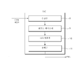
도 2는 본 발명의 제 1 실시예에 따른 타이밍 컨트롤러(TCON)를 상세히 설명하기 위한 예시도이다.2 is an exemplary view for explaining in detail the timing controller TCON according to the first embodiment of the present invention.
본 발명의 제 1 실시예에 의한 타이밍 컨트롤러(TCOM)은 한 프레임 내의 영상 데이터의 출력이 완료된 이후의 수직 블랭크 기간을 감지하여, 블랭크 신호를 출력하는 라인 카운터(4), 데이터가 표시되는 구간에는 외부로부터의 영상 데이터와 각종 제어신호와 클럭 신호를 정렬하여 출력하고, 수직 블랭크 기간에 블랭크 신호가 입력되면 이에 응답하여 특정 영상 데이터를 출력하는 데이터 설정부(5) 및 상기 각종 제어신호와 클럭신호, 영상 데이터 및 특정 영상 데이터를 입력받아 영상 데이터 패킷과 컨트롤 데이터 패킷을 생성하여 소스 드라이버 IC(SIC#1~SIC#4)로 출력하는 송신부(6)를 포함한다.The timing controller (TCOM) according to the first embodiment of the present invention detects a vertical blank period after the output of image data within one frame is completed, and outputs a blank signal to the
도 3은 본 발명의 제 1 실시예에 의한 소스 드라이버 IC(SIC#1~SIC#4)를 설명하기 위한 예시도이다.3 is an exemplary diagram for explaining the source driver ICs (
본 발명의 제 1 실시예에 의한 소스 드라이버 IC(SIC#1~SIC#4)는, 송신부(6)로부터 영상 데이터 패킷과 컨트롤 데이터 패킷을 입력받아 각종 제어 신호 및 클럭 신호를 복원하고, 영상 데이터를 병렬화하여 출력하는 수신부(8), 순차적으로 샘플링 신호를 발생하고, 상기 샘플링 신호에 대응하여 영상 데이터를 출력하는 쉬프트 레지스터(9)와, 상기 영상 데이터에 대응되는 아날로그 데이터 전압을 발생시키는 디지털-아날로그 변환부(10)와, 상기 아날로그 데이터 전압을 출력하는 출력부(11)를 포함한다.The source driver ICs (
소스 드라이버 IC(SIC#1~SIC#4)는 수직 블랭크 기간에는 상기 영상 데이터 패킷에 특정 영상 데이터가 포함되어 입력되므로, 이 때 출력부(11)는 상기 특정 영상 데이터에 대응되는 아날로그 데이터 전압을 출력한다. In the source driver ICs (
이하로는 본 발명의 제 1 실시예에 의한 표시 장치의 구동 방법을 첨부된 도면을 참조하여 상세히 설명한다.Hereinafter, a method of driving a display device according to a first embodiment of the present invention will be described in detail with reference to the accompanying drawings.
도 4는 본 발명의 제 1 실시예에 의한 표시 장치의 구동 방법을 설명하기 위한 파형도이다.4 is a waveform diagram illustrating a method of driving a display device according to a first exemplary embodiment of the present invention.
소스 드라이버 IC(SIC#1~SIC#4) 각각의 수신부(8)에는 클럭 복원 회로(미도시)가 내장되어 있다.A clock recovery circuit (not shown) is built in the
타이밍 컨트롤러(TCON)는 클럭 복원회로의 출력 위상과 주파수가 고정될 수 있도록 프리엠블 신호를 소스 드라이버 IC(SIC#1~SIC#4)들에 전송하고, 클럭 복원회로는 그 출력의 위상이 고정된 후 데이터 배선쌍(2)을 통해 프리앰블 신호와 클럭신호가 입력되면 내부 클럭을 발생시킨다.The timing controller TCON transmits the preamble signal to the source driver ICs (
소스 드라이버 IC들(SIC#1~SIC#4)은 내부 클럭의 위상과 주파수가 고정되면 출력 안정 상태를 지시하는 하이 상태의 락 신호(LOCK)를 타이밍 컨트롤러(TCON) 컨트롤러에 피드백 입력한다. 락 신호(LOCK)는 타이밍 컨트롤러(TCON)과 마지막 소스 드라이버 IC에 연결된 락 피드백 신호 배선(LOCK)을 통해 타이밍 컨트롤러(TCON)에 피드백 입력하며, 타이밍 컨트롤러(TCON)의 송신부(6)는 상기 락 신호(LOCK)를 입력받으면 소스 드라이버 IC의 수신부(8)와 데이터 링크를 형성한다.When the phase and frequency of the internal clock are fixed, the source driver
데이터 설정부(5)는 외부로부터의 영상 데이터와, 각종 클럭 신호와 제어 신호를 입력받아 이를 정렬하고 송신부(6)로 출력한다.The
송신부(6)는 상기 제어 신호 및 영상 데이터를 직렬 데이터 패킷으로 변환하고, 그에 따라 생성된 컨트롤 데이터 패킷(CTR_START~CTR2)과 영상 데이터 패킷(RGB DATA)을 소스 드라이버 IC 들(SIC#1~SIC#4)로 전송한다.The
수신부(8)는 상기 입력된 컨트롤 데이터 패킷 영상 데이터 패킷을 병렬화하여 출력한다. 상기 제어 신호들의 제어에 따라 쉬프트 레지스터(9)는 순차적으로 샘플링 신호를 발생하고, 상기 샘플링 신호에 대응하여 영상 데이터를 출력하며, 디지털-아날로그 변환부(10)는 영상 데이터에 대응되는 아날로그 데이터 전압을 발생시키고, 이 아날로그 데이터 전압은 출력부(11)를 통해 출력된다.The
라인 카운터(4)는 한 프레임 기간 내의 모든 영상 데이터의 입력이 완료된 이후인 수직 블랭크 기간(Vertical_Blank)을 감지하고 블랭크 신호를 데이터 설정부(5)로 출력한다.The
이 때 라인 카운터(4)는 외부 시스템으로부터의 데이터 인에이블 신호(DE)를 입력받아 이를 이용하여 수직 블랭크 기간(Vertical_Blank)을 감지할 수 있다. 예를 들어 상기 데이터 인에이블 신호(DE)가 입력되면 라인 카운터(4)는 1클럭의 폭을 가지는 펄스 신호를 생성하고, 상기 펄스 신호의 발생 횟수를 카운팅하며, 카운팅된 숫자가 미리 설정된 기준값에 도달한 시점을 영상 데이터 전송이 완료된 수직 블랭크 기간(Vertical_Blank)의 시점으로 판단할 수 있다.At this time, the
상기 기준값은 입력되는 영상 데이터의 해상도가 낮을수록 더 작아지며, 그에 따라 수직 블랭크 기간(Vertical_Blank)으로 판단되는 시점도 더 빨라진다.The reference value becomes smaller as the resolution of the input image data is lower, and accordingly, the time point determined as the vertical blank period (Vertical_Blank) also becomes faster.
수직 블랭크 기간(Vertical_Blank)에 데이터 설정부(5)는 상기 블랭크 신호를 입력받아 블랙 영상 데이터 또는 마지막 영상 데이터 등과 같은 특정한 영상 데이터를 송신부(6)로 출력한다.In the vertical blank period (Vertical_Blank), the
그에 따라 송신부(6)와 소스 드라이버 IC의 수신부(8), 쉬프트 레지스터(9), 디지털-아날로그 변환부(10) 및 출력부(11)는 영상 데이터 출력시와 동일한 방법으로 상기 특정 영상 데이터를 아날로그 디지털 전압으로 변환하여 출력한다.Accordingly, the
본 발명에 의한 표시 장치는 수직 블랭크 기간(Vertical_Blank)에도 블랙 영상 데이터 또는 마지막으로 입력한 영상 데이터 등의 특정 영상 데이터를 출력함으로써, 다음 프레임에 소스 드라이버 IC(SIC#1~SIC#4)에 가해지는 부하의 차이가 발생하는 문제 등을 방지하여, 표시 장치의 해상도와 입력 해상도가 상이하게 됨으로 인해 수직 블랭크 기간(Vertical_Blank)이 길어지는 경우에도 소스 드라이버 IC의 전압을 안정화시킬 수 있다.The display device according to the present invention outputs specific image data such as black image data or the last input image data even during the vertical blank period (Vertical_Blank), so that it is applied to the source driver ICs (
상기 특정 영상 데이터는 전체 수직 블랭크 기간(Vertical_Blank)에 출력될 수도 있으나, 상기 길어지는 수직 블랭크 기간의 일부(약 50% 이상)에만 출력되더라도 소스 드라이버 IC의 전압을 안정화시킬 수 있다. 이 때, 상기 특정 영상 데이터가 출력되지 않는 나머지 수직 블랭크 기간 동안 송신부(6)는 프리앰블 신호만 전송한다.Although the specific image data may be output during the entire vertical blank period (Vertical_Blank), the voltage of the source driver IC may be stabilized even if it is output only for a part (about 50% or more) of the lengthened vertical blank period. In this case, the
도 5는 본 발명의 제 2 실시예에 의한 표시 장치를 설명하기 위한 예시도이다.5 is an exemplary view for explaining a display device according to a second embodiment of the present invention.
제 2 실시예에 의한 표시 장치는 제 1 실시예와 동일하게 표시 패널(PNL), 타이밍 컨트롤러(TCON), 복수의 소스 드라이버 IC들(SIC#1~SIC#4) 및 게이트 드라이버 IC들(GIC)을 구비한다.The display device according to the second embodiment has a display panel PNL, a timing controller TCON, a plurality of source driver
타이밍 컨트롤러(TCON)는 제 1 실시예와 동일하게 테이터 배선쌍을 통해 소스 드라이버 IC들(SIC#1~SIC#4) 각각에 점-대-점 방식으로 접속된다.The timing controller TCON is connected to each of the source driver
제 2 실시예에 의한 표시 장치는 수직 블랭크 기간을 제외한 한 프레임 내의 표시 기간 중에는 제 1 실시예에 의한 표시 장치와 동일하게 구동한다.The display device according to the second embodiment operates in the same manner as the display device according to the first embodiment during the display period within one frame except for the vertical blank period.
한 프레임 내의 영상 데이터의 출력이 완료된 후인 수직 블랭크 기간에, 타이밍 컨트롤러(TCON)는 블랭크 신호를 컨트롤 데이터 패킷에 포함시켜 출력함과 아울러, 전력 소모가 가장 적은 비트를 가지도록 영상 데이터 패킷을 생성하여 소스 드라이버 IC들(SIC#1~SIC#4)로 출력한다.In the vertical blank period after the output of the image data within one frame is completed, the timing controller TCON includes the blank signal in the control data packet and outputs it, and generates the image data packet to have the least bit of power consumption. output to the source driver ICs (
소스 드라이버 IC들(SIC#1~SIC#4)은 상기 컨트롤 데이터 패킷에 포함된 블랭크 신호에 응답하여 마지막으로 출력한 영상 데이터에 대응되는 아날로그 데이터 전압을 출력한다.The source driver
도 6은 본 발명의 제 2 실시예에 의한 타이밍 컨트롤러(TCON)를 상세히 설명하기 위한 예시도이다.6 is an exemplary view for explaining in detail the timing controller TCON according to the second embodiment of the present invention.
본 발명의 제 2 실시예에 의한 타이밍 컨트롤러는, 영상 데이터 패킷이 출력되지 않는 수직 블랭크 기간을 감지하고 수직 블랭크 기간 동안 블랭크 신호(Blank_sig)를 출력하는 라인 카운터(4), 외부로부터의 영상 데이터 및 각종 컨트롤 신호들을 입력받아 정렬하여 출력하고, 수직 블랭크 기간 동안에 라인 카운터(4)로부터 블랭크 신호(Blank_sig)가 입력되면 그에 응답하여 상기 컨트롤 신호들과 최소 비트를 가진 영상 데이터를 출력하는 데이터 설정부(5) 및 표시 기간동안에는 데이터 설정부(5)로부터 영상 데이터 및 제어 신호들을 입력받아 영상 데이터 패킷과 컨트롤 데이터 패킷을 생성하여 소스 드라이버 IC들(SIC#1~SIC#4)로 출력하고, 수직 블랭크 기간 동안에는 상기 블랭크 신호(Blank_sig)를 입력받아 이를 컨트롤 데이터 패킷에 포함시켜 소스 드라이버 IC들(SIC#1~SIC#4)로 출력하는 송신부(6)를 포함한다.The timing controller according to the second embodiment of the present invention includes a
도 7은 본 발명의 제 2 실시예에 의한 소스 드라이버 IC(SIC#1~SIC#4)를 설명하기 위한 예시도이다.7 is an exemplary diagram for explaining the source driver ICs (
본 발명의 제 2 실시예에 의한 소스 드라이버 IC(SIC#1~SIC#4)는, 송신부(6)로부터 영상 데이터 패킷과 컨트롤 데이터 패킷을 입력받아 각종 제어 신호 및 클럭 신호를 복원하고, 영상 데이터를 병렬화하여 출력하는 수신부(8), 순차적으로 샘플링 신호를 발생하고, 상기 샘플링 신호에 대응하여 영상 데이터를 출력하는 쉬프트 레지스터(9)와, 상기 영상 데이터에 대응되는 아날로그 데이터 전압을 발생시키는 디지털-아날로그 변환부(10)와, 상기 아날로그 데이터 전압을 출력하는 출력부(11)를 포함한다.The source driver ICs (
수직 블랭크 기간에는 상기 영상 데이터 패킷에 블랭크 신호(Blank_sig)가 포함되어 입력되며, 이 때 수신부(8)는 상기 블랭크 신호(Blank_sig)를 출력부(11)로 전달한다.During the vertical blank period, a blank signal (Blank_sig) is included in the image data packet and is input. At this time, the
출력부(11)는 블랭크 신호(Blank_sig)에 응답하여 마지막으로 출력한 아날로그 데이터 전압을 다시 출력한다.The
도 8은 본 발명의 제 2 실시예에 의한 표시 장치의 구동 방법을 설명하기 위한 파형도이다.8 is a waveform diagram illustrating a method of driving a display device according to a second exemplary embodiment of the present invention.
표시 기간 중 본 발명의 제 2 실시예에 의한 표시 장치의 구동 방법은 제 1 실시예에 의한 표시 장치의 구동 방법과 동일하며, 수직 블랭크 기간(Vertical_Blank)중의 구동에 있어서 제 1 실시예에 의한 표시 장치의 구동 방법과 차이가 있다.The driving method of the display device according to the second embodiment of the present invention during the display period is the same as the driving method of the display device according to the first embodiment, and the display according to the first embodiment in driving during the vertical blank period (Vertical_Blank) There is a difference in the method of operating the device.
본 발명의 제 2 실시예에 의한 라인 카운터(4)는 제 1 실시예에 의한 라인 카운터와 동일한 방법으로 수직 블랭크 기간(Vertical_Blank)을 감지하고, 블랭크 신호(Blank_sig)를 데이터 설정부(5)와 송신부(6)로 출력한다.The
데이터 설정부(5)는 블랭크 신호(Blank_sig)에 응답하여 영상 데이터의 출력을 중단한다.The
송신부(6)는 상기 블랭크 신호(Blank_sig)를 입력받아, 이를 컨트롤 데이터에 포함시켜 컨트롤 데이터 패킷을 생성하며, 최소 비트수를 가지는 영상 데이터 패킷을 생성하여 소스 드라이버 IC(SIC#1~SIC#4)로 출력한다.The
소스 드라이버 IC(SIC#1~SIC#4)의 수신부(8)는 상기 컨트롤 데이터 패킷에 블랭크 신호(Blank_sig)가 포함된 경우, 상기 블랭크 신호(Blank_sig)를 출력부(11)로 공급한다.The receiving
출력부(11)는 상기 블랭크 신호에 응답하여 마지막으로 출력한 아날로그 데이터 전압을 표시 패널(PNL)로 출력한다.The
본 발명의 제 2 실시예에 의하면, 송신부(6)는 수직 블랭크 기간(Vertical_Blank) 동안 데이터 트랜지션이 가장 적게 일어나는 영상 데이터 패킷을 생성하여 수신부(8)로 출력하므로, 표시 장치의 소비전력을 줄일 수 있는 효과가 있다.According to the second embodiment of the present invention, since the
상기 특정 영상 데이터는 전체 수직 블랭크 기간(Vertical_Blank)에 출력될 수도 있으나, 상기 길어지는 수직 블랭크 기간의 일부(약 50% 이상)에만 출력되더라도 소스 드라이버 IC의 전압을 안정화시킬 수 있다. 이 때, 상기 특정 영상 데이터가 출력되지 않는 나머지 수직 블랭크 기간 동안 송신부(6)는 프리앰블 신호만 전송한다.Although the specific image data may be output during the entire vertical blank period (Vertical_Blank), the voltage of the source driver IC may be stabilized even if it is output only for a part (about 50% or more) of the lengthened vertical blank period. In this case, the
도 9는 본 발명의 제 3 실시예에 의한 표시 장치를 설명하기 위한 예시도이다.9 is an exemplary view for explaining a display device according to a third embodiment of the present invention.
본 발명의 제 3 실시예에 의한 표시 장치는, 표시 패널(PNL), 타이밍 컨트롤러(TCON), 복수의 소스 드라이버 IC들(SIC#1~SIC#4) 및 게이트 드라이버 IC들(GIC)을 구비한다.A display device according to a third embodiment of the present invention includes a display panel PNL, a timing controller TCON, a plurality of source driver
타이밍 컨트롤러(TCON)는 데이터 배선쌍(2)을 통해 소스 드라이버 IC들(SIC#1~SIC#4) 각각에 점-대-점 방식으로 접속되어 있는 점에 있어서는 상기 제 1 및 제 2 실시예와 동일하며, 제 3 실시예에 의한 타이밍 컨트롤러(TCON)는 별도의 블랭크 라인(10)을 통해 각 소스 드라이버 IC들(SIC#1~SIC#4)과 추가로 접속된다. The timing controller TCON is connected to each of the source driver
본 발명의 제 3 실시예에 의한 타이밍 컨트롤러(TOCN)는 수직 블랭크 기간에 블랭크 라인(10)을 통해 블랭크 신호를 직접 소스 드라이버 IC로 전송하고, 소스 드라이버 IC는 블랭크 신호에 응답하여 마지막으로 출력한 아날로그 데이터 전압을 출력하는 특징을 가진다.The timing controller (TOCN) according to the third embodiment of the present invention directly transmits the blank signal to the source driver IC through the
도 10은 본 발명의 제 3 실시예에 의한 타이밍 컨트롤러(TCON)를 설명하기 위한 예시도이다.10 is an exemplary diagram for explaining a timing controller TCON according to a third embodiment of the present invention.
본 발명의 제 3 실시예에 의한 타이밍 컨트롤러(TCON)는, 영상 데이터 패킷이 출력되지 않는 수직 블랭크 기간을 감지하고 수직 블랭크 기간(Vertical_Blank) 동안 블랭크 라인(10)으로 블랭크 신호를 출력하는 라인 카운터(4), 외부로부터의 영상 데이터 및 각종 컨트롤 신호들을 입력받아 정렬하여 출력하고, 수직 블랭크 기간 동안에 라인 카운터(4)로부터 블랭크 신호가 입력되면 그에 응답하여 영상 데이터 및 제어 신호를 출력하지 않는 데이터 설정부(5) 및 표시 기간동안에는 데이터 설정부(5)로부터 영상 데이터 및 제어 신호들을 입력받아 영상 데이터 패킷과 컨트롤 데이터 패킷을 생성하여 소스 드라이버 IC들(SIC#1~SIC#4)로 출력하고, 수직 블랭크 기간(Vertical_Blank)에는 상기 데이터 패킷 내에 프리앰블 신호만 포함하여 출력하는 송신부(6)를 포함한다.The timing controller TCON according to the third embodiment of the present invention detects a vertical blank period in which an image data packet is not output and outputs a blank signal to the
도 11은 본 발명의 제 3 실시예에 의한 소스 드라이버 IC를 설명하기 위한 예시도이다.11 is an exemplary diagram for explaining a source driver IC according to a third embodiment of the present invention.
본 발명의 제 3 실시예에 의한 소스 드라이버 IC는(SIC#1~SIC#4)는, 송신부(6)로부터 영상 데이터 패킷과 컨트롤 데이터 패킷을 입력받아 각종 제어 신호 및 클럭 신호를 복원하고, 영상 데이터를 병렬화하여 출력하는 수신부(8), 순차적으로 샘플링 신호를 발생하고, 상기 샘플링 신호에 대응하여 영상 데이터를 출력하는 쉬프트 레지스터(9)와, 상기 영상 데이터에 대응되는 아날로그 데이터 전압을 발생시키는 디지털-아날로그 변환부(10)와, 상기 아날로그 데이터 전압을 출력하는 출력부(11)를 포함하는 점에 있어서는 상기 제 1 및 제 2 실시예와 같다.The source driver ICs (
블랭크 라인(10)은 타이밍 컨트롤러(TCON)의 라인 카운터(4)와 소스 드라이버 IC(SIC#1~SIC#4)의 출력부(11)에 접속된다. The
본 발명의 제 3 실시예에 의한 표시 장치의 수직 블랭크 기간을 제외한 나머지 기간의 구동 방법은 제 1 및 제 2 실시예와 동일하다.The driving method for the remaining periods except for the vertical blank period of the display device according to the third embodiment of the present invention is the same as that of the first and second embodiments.
수직 블랭크 기간에 라인 카운터(4)는 블랭크 라인(10)을 통해 출력부(11)로 블랭크 신호를 직접 출력함과 동시에 데이터 설정부(5)로도 블랭크 신호를 출력한다.During the vertical blank period, the
데이터 설정부(5)는 수직 블랭크 기간 동안에 라인 카운터(4)로부터 블랭크 신호가 입력되면 그에 응답하여 영상 데이터 및 제어 신호를 출력하지 않는다.When a blank signal is input from the
그에 따라 송신부(6)는 수직 블랭크 기간에는 컨트롤 데이터 패킷 및 영상 데이터 패킷을 출력하지 않고, 프리앰블 신호만을 출력한다.Accordingly, the
출력부(11)는 라인 카운터(4)로부터의 블랭크 신호에 응답하여 마지막으로 출력한 아날로그 데이터 전압을 출력한다.The
실시예 3 에 의하면, 송신부(6)는 수직 블랭크 기간에 컨트롤 데이터 패킷 및 영상 데이터 패킷을 출력하지 않음으로써 표시 장치의 소비 전력을 크게 줄일 수 있는 효과를 가진다.According to the third embodiment, the
이 때 출력부(11)는 전체 수직 블랭크 기간에 아날로그 데이터 전압을 출력할 수도 있으나, 수직 블랭크 기간의 일부(약 50% 이상)만 아날로그 데이터 전압을 출력하더라도 소스 드라이버 IC를 상당히 안정화시킬 수 있다. In this case, the
도 12는 본 발명의 제 4 실시예에 의한 표시 장치를 설명하기 위한 예시도이다.12 is an exemplary view for explaining a display device according to a fourth embodiment of the present invention.
본 발명의 제 4 실시예에 의한 표시 장치에 구비된 타이밍 컨트롤러(TCON)는 표시 패널(PNL), 타이밍 컨트롤러(TCON), 복수의 소스 드라이버 IC들(SIC#1~SIC#4) 및 게이트 드라이버 IC들(GIC)을 구비한다.The timing controller TCON included in the display device according to the fourth embodiment of the present invention includes a display panel PNL, a timing controller TCON, a plurality of source driver
타이밍 컨트롤러(TCON)는 데이터 배선쌍(2)을 통해 소스 드라이버 IC들(SIC#1~SIC#4) 각각에 점-대-점 방식으로 접속되어 있는 점에 있어서는 상기 제 1 내지 제 3 실시예와 동일하다.The timing controller TCON is connected to each of the source driver
본 발명의 제 4 실시예에 의한 타이밍 컨트롤러(TCON)는 수직 블랭크 기간에는 영상 데이터 및 컨트롤 신호를 출력하지 않는다.The timing controller TCON according to the fourth embodiment of the present invention does not output image data and control signals during the vertical blank period.
또한 소스 드라이버 IC들(SIC#1~SIC#4) 각각은 자체적으로 수직 블랭크 기간을 감지하고, 수직 블랭크 기간에는 마지막으로 출력한 아날로그 데이터 전압을 출력한다.In addition, each of the source driver
도 13은 본 발명의 제 4 실시예에 의한 타이밍 컨트롤러(TCON)를 설명하기 위한 예시도이다.13 is an exemplary diagram for explaining a timing controller TCON according to a fourth embodiment of the present invention.
본 발명의 제 4 실시예에 의한 타이밍 컨트롤러(TCON)는, 영상 데이터 패킷이 출력되지 않는 수직 블랭크 기간을 감지하고 수직 블랭크 기간 동안 블랭크 신호를 출력하는 라인 카운터(4), 외부로부터의 영상 데이터 및 각종 컨트롤 신호들을 입력받아 정렬하여 출력하고, 수직 블랭크 기간 동안에 라인 카운터(4)로부터 블랭크 신호가 입력되면 그에 응답하여 영상 데이터 및 제어 신호를 출력하지 않는 데이터 설정부(5) 및 표시 기간동안에는 데이터 설정부(5)로부터 영상 데이터 및 제어 신호들을 입력받아 영상 데이터 패킷과 컨트롤 데이터 패킷을 생성하여 소스 드라이버 IC들(SIC#1~SIC#4)로 출력하고, 수직 블랭크 기간에는 상기 데이터 패킷 내에 프리앰블 신호만 포함하여 출력하는 송신부(6)를 포함한다.The timing controller TCON according to the fourth embodiment of the present invention includes a
도 14는 본 발명의 제 4 실시예에 의한 소스 드라이버 IC를 설명하기 위한 예시도이다.14 is an exemplary diagram for explaining a source driver IC according to a fourth embodiment of the present invention.
본 발명의 제 4 실시예에 의한 소스 드라이버 IC는 송신부(6)로부터 영상 데이터 패킷과 컨트롤 데이터 패킷을 입력받아 각종 제어 신호 및 클럭 신호를 복원하고, 영상 데이터를 병렬화하여 출력하는 수신부(8), 순차적으로 샘플링 신호를 발생하고, 상기 샘플링 신호에 대응하여 영상 데이터를 출력하는 쉬프트 레지스터(9)와, 상기 영상 데이터에 대응되는 아날로그 데이터 전압을 발생시키는 디지털-아날로그 변환부(10)와, 상기 아날로그 데이터 전압을 출력하는 출력부(11)를 포함한다.The source driver IC according to the fourth embodiment of the present invention includes a
또한, 본 발명의 제 4 실시예에 의한 소스 드라이버 IC는, 송신부(6)로부터 컨트롤 패킷이 전송되지 않음으로써 컨트롤 신호의 입력이 중단되는 기간을 수직 블랭크 기간으로 판단하여 출력부(11)가 마지막으로 출력한 아날로그 영상 데이터를 출력하도록 상기 출력부(11)를 제어하는 블랭크 감지부(12)를 더 포함한다.In addition, in the source driver IC according to the fourth embodiment of the present invention, the period in which the input of the control signal is stopped due to no control packet being transmitted from the
본 발명의 제 4 실시예에 의한 표시 장치의 수직 블랭크 기간을 제외한 나머지 기간의 구동 방법은 제 1 및 제 2 실시예와 동일하다.The driving method for the remaining periods except for the vertical blank period of the display device according to the fourth embodiment of the present invention is the same as that of the first and second embodiments.
수직 블랭크 기간에 라인 카운터(4)는 데이터 설정부(5)로 블랭크 신호를 출력한다.In the vertical blank period, the
데이터 설정부(5)는 수직 블랭크 기간 동안에 라인 카운터(4)로부터 블랭크 신호가 입력되면 그에 응답하여 영상 데이터 및 제어 신호를 출력하지 않는다.When a blank signal is input from the
그에 따라 송신부(6)는 수직 블랭크 기간에는 컨트롤 데이터 패킷 및 영상 데이터 패킷을 출력하지 않고, 프리앰블 신호만을 출력한다.Accordingly, the
블랭크 감지부(12)는 수신부(7)로 입력되는 컨트롤 데이터 패킷에 포함된 복수의 제어 신호들을 수신부(7)로부터 입력받으며, 제어 신호들이 일정 기간 이상 입력되지 않는 기간을 수직 블랭크 기간으로 감지한다.The
이 때 블랭크 감지부(12)는 수신부(7)로부터 출력되는 복수의 제어 신호 중 어느 하나를 기준으로 상기 수직 블랭크 기간을 감지할 수 있다. 예를 들어 블랭크 감지부(12)는 소스 아웃풋 인에이블(SOE) 신호의 입력 여부를 감지하고, 일정 기간 이상 소스 아웃풋 인에이블(SOE) 신호가 미입력되는 기간을 수직 블랭크 기간으로 할 수 있다.At this time, the
블랭크 감지부(12)는 수직 블랭크 기간으로 감지한 시점에는 출력부(11)가 마지막으로 출력된 아날로그 데이터 전압을 출력하도록 상기 출력부(11)를 제어한다.The
그에 따라 본 발명의 제 4 실시예에 의한 표시 장치는, 소스 드라이버 IC(SIC#1~SIC#4) 내부에서 수직 블랭크 기간을 직접 인지하고, 마지막으로 출력된 아날로그 데이터 전압을 출력하는 특징을 가지며, 타이밍 컨트롤러(TCON)는 수직 블랭크 기간에 컨트롤 데이터 패킷 및 영상 데이터 패킷을 생성, 출력하지 않으므로 소비 전력이 감소하는 효과가 있다.Accordingly, the display device according to the fourth embodiment of the present invention has a feature of directly recognizing the vertical blank period inside the source driver ICs (
이 때 출력부(11)는 전체 수직 블랭크 기간에 아날로그 데이터 전압을 출력할 수도 있으나, 수직 블랭크 기간의 일부(약 50% 이상)만 아날로그 데이터 전압을 출력하더라도 소스 드라이버 IC를 상당히 안정화시킬 수 있다.In this case, the
도 15는 수직 블랭크 기간 동안 소스 드라이버 IC 가 데이터 전압을 출력하지 않은 경우와 본 발명에 의해 소스 드라이버 IC 가 수직 블랭크 기간 동안 데이터 전압을 출력한 경우의 구동 전압의 흔들림을 비교한 것이다.15 is a comparison of the fluctuation of the driving voltage when the source driver IC does not output the data voltage during the vertical blank period and when the source driver IC outputs the data voltage during the vertical blank period according to the present invention.
수직 블랭크 기간 동안 소스 드라이버 IC가 데이터 전압을 출력하지 않은 경우에는 최대 데이터 전압과 최소 데이터 전압의 차이가 1.2V 가 발생(도 15의 (b) 참조)하며, 구동 전압이 불안정한 현상이 발생했으나, 수직 블랭크 기간 동안 소스 드라이버 IC가 데이터 전압을 출력한 경우에는 최대 데이터 전압과 최소 데이터 전압의 차이가 0.5V(도 15의 (a) 참조)로 상당히 안정된 것을 알 수 있다.When the source driver IC does not output the data voltage during the vertical blank period, the difference between the maximum data voltage and the minimum data voltage is 1.2V (see Fig. 15 (b)), and the driving voltage is unstable. When the source driver IC outputs the data voltage during the vertical blank period, it can be seen that the difference between the maximum data voltage and the minimum data voltage is 0.5V (refer to FIG. 15(a) ), which is quite stable.
지금까지 살펴본 바와 같이, 본 발명의 제 1 내지 제 4 실시예에 의한 표시 장치는, EPI 인터페이스 방식을 사용하며, 수직 블랭크 기간 동안에도 소스 드라이버 IC 가 특정 데이터를 출력하도록 함으로써, 표시 장치의 해상도와 입력 해상도가 상이한 경우에도 소스 드라이버 IC의 구동 전압을 안정화할 수 있다.As described so far, the display device according to the first to fourth embodiments of the present invention uses the EPI interface method and allows the source driver IC to output specific data even during the vertical blank period, thereby increasing the resolution of the display device and Even when the input resolution is different, the driving voltage of the source driver IC can be stabilized.
이 때 수직 블랭크 기간 전체에서 상기 소스 드라이버 IC 가 특정 데이터를 출력할 수도 있지만, 전체 수직 블랭크 기간 중 약 50% 정도의 기간 이상 특정 데이터를 출력한다면 상기의 구동 전압 안정화 효과를 얻을 수 있다.In this case, the source driver IC may output specific data during the entire vertical blank period, but if the specific data is output for about 50% or more of the entire vertical blank period, the driving voltage stabilization effect may be obtained.
이상에서 본 발명의 기술적 사상을 예시하기 위해 구체적인 실시예로 도시하고 설명하였으나, 본 발명은 상기와 같이 구체적인 실시예와 동일한 구성 및 작용에만 국한되지 않고, 여러 가지 변형이 본 발명의 기술적 사상을 벗어나지 않는 범위 내에서 실시될 수 있다. 따라서, 그와 같은 변형도 본 발명의 범위에 속하는 것으로 간주해야 하며, 본 발명의 범위는 후술하는 특허청구범위에 의해 결정되어야 한다.In the above, it has been shown and described as a specific embodiment to illustrate the technical idea of the present invention, but the present invention is not limited to the same configuration and operation as the specific embodiment as described above, and various modifications do not deviate from the technical spirit of the present invention. It can be carried out within the scope that does not. Accordingly, such modifications should also be considered to fall within the scope of the present invention, and the scope of the present invention should be determined by the following claims.
2: 데이터 배선쌍 4: 라인 카운터
5: 데이터 설정부 6: 송신부
7: 시스템 8: 수신부
9: 쉬프트 레지스터 10: 디지털 아날로그 변환부
11: 출력부 12: 블랭크 감지부2: Data wire pair 4: Line counter
5: Data setting unit 6: Transmitting unit
7: System 8: Receiver
9: shift register 10: digital-to-analog converter
11: output unit 12: blank detection unit
Claims (18)
상기 타이밍 컨트롤러와 점 대 점 방식으로 연결되는 복수의 소스 드라이버 IC를 포함하고,
상기 타이밍 컨트롤러는 상기 타이밍 컨트롤러와 각 소스 드라이버 IC 를 연결하는 데이터 배선쌍을 통해 정렬된 영상 데이터와 제어 신호 및 클럭 신호를 영상 데이터 패킷 및 컨트롤 데이터 패킷으로 변환하여 상기 각 소스 드라이버 IC로 전송하는 EPI 전송방식을 이용하여 상기 각 소스 드라이버 IC들에 상기 영상 데이터 패킷 및 컨트롤 데이터 패킷을 공급하고,
영상 데이터를 표시하지 않는 수직 블랭크 기간에는 상기 각 소스 드라이버 IC들에 특정 영상 데이터를 출력하며,
상기 각 소스 드라이버 IC들은, 상기 영상 데이터 패킷에 포함된 영상 데이터 또는 특정 영상 데이터를 아날로그 데이터 전압으로 변환하여 상기 소스 드라이버 IC들에 접속된 각 데이터 라인에 공급하고,
상기 타이밍 컨트롤러는,
상기 영상 데이터 패킷이 출력되지 않는 수직 블랭크 기간을 감지하여 상기 수직 블랭크 기간에 블랭크 신호를 출력하는 라인 카운터,
외부로부터 영상 데이터 및 각종 클럭 신호를 입력받아 정렬하여 출력하며, 상기 라인 카운터로부터 상기 블랭크 신호가 입력되면 상기 특정 영상 데이터를 출력하는 데이터 설정부, 및
상기 데이터 설정부로부터 상기 영상 데이터 및 각종 클럭 신호를 입력받아 영상 데이터 패킷 및 컨트롤 데이터 패킷을 생성하여 출력하거나, 상기 수직 블랭크 기간에는 상기 특정 영상 데이터를 입력받아 특정 영상 데이터 패킷을 생성하여 상기 각 소스 드라이버 IC로 출력하는 송신부를 포함하는 표시 장치.a timing controller that aligns image data from the outside and controls display timing of the image; and
a plurality of source driver ICs connected to the timing controller in a point-to-point manner;
The timing controller converts image data, control signals, and clock signals aligned through a pair of data wires connecting the timing controller and each source driver IC into image data packets and control data packets and transmits them to each source driver IC. supplying the image data packet and the control data packet to each of the source driver ICs using a transmission method;
In the vertical blank period in which no image data is displayed, specific image data is output to each of the source driver ICs,
each of the source driver ICs converts image data or specific image data included in the image data packet into an analog data voltage and supplies it to each data line connected to the source driver ICs;
The timing controller is
a line counter detecting a vertical blank period in which the image data packet is not output and outputting a blank signal in the vertical blank period;
a data setting unit for receiving image data and various clock signals from the outside, arranging and outputting them, and outputting the specific image data when the blank signal is input from the line counter; and
The image data and various clock signals are received from the data setting unit, and an image data packet and a control data packet are generated and output, or during the vertical blank period, the specific image data is received and a specific image data packet is generated to generate a specific image data packet for each source. A display device including a transmitter that outputs to a driver IC.
상기 복수의 소스 드라이버 IC 각각은,
상기 송신부로부터 상기 컨트롤 데이터 패킷, 상기 영상 데이터 패킷 또는 상기 특정 영상 데이터 패킷을 수신받아 각종 클럭 신호를 복원하고, 상기 영상 데이터 또는 상기 특정 영상 데이터를 병렬화하여 출력하는 수신부를 포함하는 표시 장치.The method of claim 1,
Each of the plurality of source driver ICs,
and a receiver configured to receive the control data packet, the image data packet, or the specific image data packet from the transmitter, restore various clock signals, and parallelize and output the image data or the specific image data.
상기 타이밍 컨트롤러와 점 대 점 방식으로 연결되는 복수의 소스 드라이버 IC를 포함하고,
상기 타이밍 컨트롤러는 상기 각 소스 드라이버 IC 들과 점 대 점 방식으로 연결되며, 상기 타이밍 컨트롤러는 상기 타이밍 컨트롤러와 각 소스 드라이버 IC 를 연결하는 데이터 배선쌍을 통해 정렬된 영상 데이터와 제어 신호 및 클럭 신호를 영상 데이터 패킷 및 컨트롤 데이터 패킷으로 변환하여 상기 각 소스 드라이버 IC로 전송하는 EPI 전송방식을 이용하여 상기 각 소스 드라이버 IC들에 상기 영상 데이터 패킷 및 컨트롤 데이터 패킷을 공급하고,
영상 데이터를 표시하지 않는 수직 블랭크 기간에는 상기 각 소스 드라이버 IC가 특정 데이터를 출력하도록 상기 소스 드라이버 IC들을 제어하는 블랭크 신호를 상기 컨트롤 데이터 패킷에 포함시켜 출력하고,
상기 각 소스 드라이버 IC들은, 상기 수직 블랭크 기간에는 상기 컨트롤 데이터 패킷에 포함된 상기 블랭크 신호에 응답하여 마지막으로 출력한 데이터를 출력하고,
상기 타이밍 컨트롤러는,
상기 영상 데이터 패킷이 출력되지 않는 수직 블랭크 기간을 감지하여 상기 수직 블랭크 기간에 블랭크 신호를 출력하는 라인 카운터,
외부로부터의 영상 데이터 및 각종 컨트롤 신호들을 입력받아 정렬하여 출력하고, 상기 라인 카운터로부터 상기 블랭크 신호가 입력되면 최소 비트수를 가지는 영상 데이터 및 상기 컨트롤 신호를 생성하는 데이터 설정부, 및
상기 데이터 설정부에서 정렬된 영상 데이터 및 제어 신호들을 입력받아 영상 데이터 패킷, 컨트롤 데이터 패킷을 생성하여 상기 각 소스 드라이버 IC로 출력하고, 상기 라인 카운터로부터 상기 블랭크 신호를 입력받아 상기 블랭크 신호가 포함된 상기 컨트롤 데이터 패킷을 생성하여 상기 소스 드라이버 IC로 출력하는 송신부를 포함하는 표시 장치.a timing controller that aligns image data from the outside and controls display timing of the image; and
a plurality of source driver ICs connected to the timing controller in a point-to-point manner;
The timing controller is connected to each of the source driver ICs in a point-to-point manner, and the timing controller transmits image data, a control signal, and a clock signal aligned through a data wire pair connecting the timing controller and each source driver IC. supplying the image data packet and the control data packet to each of the source driver ICs using an EPI transmission method in which an image data packet and a control data packet are converted and transmitted to each source driver IC;
In a vertical blank period in which image data is not displayed, a blank signal for controlling the source driver ICs to output specific data is included in the control data packet and outputted;
Each of the source driver ICs outputs last output data in response to the blank signal included in the control data packet during the vertical blank period;
The timing controller is
a line counter detecting a vertical blank period in which the image data packet is not output and outputting a blank signal in the vertical blank period;
a data setting unit for receiving image data and various control signals from the outside, sorting and outputting them, and generating image data having a minimum number of bits and the control signal when the blank signal is input from the line counter; and
The image data and control signals arranged in the data setting unit are received, an image data packet and a control data packet are generated and outputted to each source driver IC, and the blank signal is received from the line counter and the blank signal is included. and a transmitter to generate the control data packet and output the generated control data packet to the source driver IC.
상기 소스 드라이버 IC는,
상기 컨트롤 데이터 패킷 및 상기 영상 데이터 패킷을 입력받아 이를 병렬화하고 각종 클럭 신호들을 복원하는 수신부, 및
상기 컨트롤 데이터 패킷에 블랭크 신호가 포함된 경우, 상기 수신부로부터 상기 블랭크 신호를 입력받아 마지막으로 출력된 데이터 전압을 출력하는 출력부를 포함하는 표시 장치.5. The method of claim 4,
The source driver IC,
a receiving unit that receives the control data packet and the image data packet, parallelizes them, and restores various clock signals; and
and an output unit for receiving the blank signal from the receiving unit and outputting a last data voltage when the control data packet includes a blank signal.
상기 타이밍 컨트롤러와 점 대 점 방식으로 연결되는 복수의 소스 드라이버 IC를 포함하고,
상기 타이밍 컨트롤러는 상기 타이밍 컨트롤러와 각 소스 드라이버 IC 를 연결하는 데이터 배선쌍을 통해 정렬된 영상 데이터와 제어 신호 및 클럭 신호를 영상 데이터 패킷 및 컨트롤 데이터 패킷으로 변환하여 상기 각 소스 드라이버 IC로 전송하는 EPI 전송방식을 이용하여 상기 각 소스 드라이버 IC들에 상기 영상 데이터 패킷 및 컨트롤 데이터 패킷을 공급하고,
영상 데이터를 표시하지 않는 수직 블랭크 기간에는 상기 영상 데이터 패킷 및 상기 컨트롤 데이터 패킷의 전송을 중단하고,
상기 각 소스 드라이버 IC들과 상기 타이밍 컨트롤러 사이에는 블랭크 신호 전송 라인이 더 접속되고, 상기 수직 블랭크 기간에 상기 각 소스 드라이버 IC들은 상기 블랭크 신호 전송 라인을 통해 공급되는 블랭크 신호에 응답하여 마지막으로 출력된 데이터 전압을 출력하는 표시 장치.a timing controller that aligns image data from the outside and controls display timing of the image; and
a plurality of source driver ICs connected to the timing controller in a point-to-point manner;
The timing controller converts image data, control signals, and clock signals aligned through a pair of data wires connecting the timing controller and each source driver IC into image data packets and control data packets and transmits them to each source driver IC. supplying the image data packet and the control data packet to each of the source driver ICs using a transmission method;
In a vertical blank period in which no image data is displayed, the transmission of the image data packet and the control data packet is stopped;
A blank signal transmission line is further connected between each of the source driver ICs and the timing controller, and in the vertical blank period, each of the source driver ICs is finally output in response to a blank signal supplied through the blank signal transmission line. A display device that outputs a data voltage.
상기 타이밍 컨트롤러는,
상기 영상 데이터 패킷이 출력되지 않는 수직 블랭크 기간을 감지하여 상기 수직 블랭크 기간에 블랭크 신호를 출력하는 라인 카운터,
외부로부터의 영상 데이터 및 각종 컨트롤 신호들을 입력받아 정렬하여 출력하고, 상기 라인 카운터로부터 상기 블랭크 신호가 입력되면 상기 영상 데이터 및 컨트롤 신호들의 출력을 중단하는 데이터 설정부, 및
상기 데이터 설정부에서 정렬된 영상 데이터 및 제어 신호들을 입력받아 영상 데이터 패킷, 컨트롤 데이터 패킷을 생성하여 상기 각 소스 드라이버 IC로 출력하고, 상기 수직 블랭크 기간에는 상기 컨트롤 데이터 패킷 및 상기 영상 데이터 패킷의 출력을 중단하는 송신부를 포함하는 표시 장치.8. The method of claim 7,
The timing controller is
a line counter detecting a vertical blank period in which the image data packet is not output and outputting a blank signal in the vertical blank period;
a data setting unit for receiving image data and various control signals from the outside, arranging and outputting them, and stopping the output of the image data and control signals when the blank signal is input from the line counter; and
The image data and control signals arranged in the data setting unit are received, an image data packet and a control data packet are generated and outputted to each of the source driver ICs, and the control data packet and the image data packet are outputted during the vertical blank period. A display device including a transmitter to stop the.
상기 소스 드라이버 IC 각각은,
상기 컨트롤 데이터 패킷 및 상기 영상 데이터 패킷을 입력받아 이를 병렬화하고 각종 클럭 신호들을 복원하는 수신부, 및
상기 수신부에서 복원된 영상 데이터를 출력하거나, 상기 블랭크 신호 전송 라인을 통해 공급되는 블랭크 신호에 응답하여 마지막으로 출력된 데이터 전압을 출력하는 출력부를 포함하는 표시 장치.9. The method of claim 8,
Each of the source driver ICs,
a receiving unit that receives the control data packet and the image data packet, parallelizes them, and restores various clock signals; and
and an output unit outputting the image data restored by the receiving unit or outputting a data voltage finally output in response to a blank signal supplied through the blank signal transmission line.
상기 타이밍 컨트롤러와 점 대 점 방식으로 연결되는 복수의 소스 드라이버 IC를 포함하고,
상기 타이밍 컨트롤러는 상기 각 소스 드라이버 IC 들과 점 대 점 방식으로 연결되며, 상기 타이밍 컨트롤러는 상기 타이밍 컨트롤러와 각 소스 드라이버 IC 를 연결하는 데이터 배선쌍을 통해 정렬된 영상 데이터와 제어 신호 및 클럭 신호를 영상 데이터 패킷 및 컨트롤 데이터 패킷으로 변환하여 상기 각 소스 드라이버 IC로 전송하는 EPI 전송방식을 이용하여 상기 각 소스 드라이버 IC들에 상기 영상 데이터 패킷 및 컨트롤 데이터 패킷을 공급하고,
영상 데이터를 표시하지 않는 수직 블랭크 기간에는 상기 영상 데이터 패킷 및 상기 컨트롤 데이터 패킷의 전송을 중단하고,
상기 각 소스 드라이버 IC들은, 상기 수직 블랭크 기간에 상기 소스 드라이버 IC는 상기 타이밍 컨트롤러로부터 컨트롤 신호의 입력이 일정 기간 동안 중단될 경우, 마지막으로 출력된 데이터 전압을 출력하는 표시 장치.a timing controller that aligns image data from the outside and controls display timing of the image; and
a plurality of source driver ICs connected to the timing controller in a point-to-point manner;
The timing controller is connected to each of the source driver ICs in a point-to-point manner, and the timing controller transmits image data, a control signal, and a clock signal aligned through a data wire pair connecting the timing controller and each source driver IC. supplying the image data packet and the control data packet to each of the source driver ICs using an EPI transmission method in which an image data packet and a control data packet are converted and transmitted to each source driver IC;
In a vertical blank period in which no image data is displayed, the transmission of the image data packet and the control data packet is stopped;
In each of the source driver ICs, in the vertical blank period, when input of a control signal from the timing controller is stopped for a predetermined period, the source driver IC outputs a last data voltage.
상기 타이밍 컨트롤러는,
상기 영상 데이터 패킷이 출력되지 않는 수직 블랭크 기간을 감지하여 상기 수직 블랭크 기간에 블랭크 신호를 출력하는 라인 카운터,
외부로부터의 영상 데이터 및 각종 컨트롤 신호들을 입력받아 정렬하여 출력하고, 상기 라인 카운터로부터 상기 블랭크 신호가 입력되면 상기 영상 데이터 및 컨트롤 신호들의 출력을 중단하는 데이터 설정부, 및
상기 데이터 설정부에서 정렬된 영상 데이터 및 제어 신호들을 입력받아 영상 데이터 패킷, 컨트롤 데이터 패킷을 생성하여 상기 각 소스 드라이버 IC로 출력하고, 상기 수직 블랭크 기간에는 상기 컨트롤 데이터 패킷 및 상기 영상 데이터 패킷의 출력을 중단하는 송신부를 포함하는 표시 장치.11. The method of claim 10,
The timing controller is
a line counter detecting a vertical blank period in which the image data packet is not output and outputting a blank signal in the vertical blank period;
a data setting unit for receiving image data and various control signals from the outside, arranging and outputting them, and stopping the output of the image data and control signals when the blank signal is input from the line counter; and
The image data and control signals arranged in the data setting unit are received, an image data packet and a control data packet are generated and outputted to each of the source driver ICs, and the control data packet and the image data packet are outputted during the vertical blank period. A display device including a transmitter to stop the.
상기 각 소스 드라이버 IC는,
상기 컨트롤 데이터 패킷 중 소스 출력 인에이블 신호의 전송이 중단된 기간이 미리 입력된 일정 기간을 초과한 경우를 수직 블랭크 기간으로 감지하는 블랭크 감지부, 및
상기 블랭크 기간으로 감지된 기간에는 마지막으로 출력된 데이터 전압을 출력하는 출력부를 포함하는 표시 장치.12. The method of claim 11,
Each of the source driver ICs,
a blank detection unit for detecting a case in which a period during which transmission of a source output enable signal is stopped in the control data packet exceeds a predetermined period input in advance as a vertical blank period; and
and an output unit configured to output a last data voltage output during the period sensed as the blank period.
상기 라인 카운터는
데이터인에이블 신호를 입력받아 1클럭의 폭을 가지는 복수의 펄스 신호를 생성하고, 상기 펄스 신호의 수를 카운팅하여 미리 설정된 소정의 펄스 신호수에 도달하는 시점을 수직 블랭크 기간의 시점으로 감지하는 표시 장치.12. The method of any one of claims 1, 4, 8, 11,
The line counter is
A display device that receives a data enable signal, generates a plurality of pulse signals having a width of one clock, counts the number of pulse signals, and detects a time point reaching a preset number of pulse signals as a start point of a vertical blank period .
상기 타이밍 컨트롤러는,
상기 영상 데이터 패킷이 출력되지 않는 수직 블랭크 기간을 감지하여 상기 수직 블랭크 기간에 블랭크 신호를 출력하는 라인 카운터,
외부로부터 영상 데이터 및 각종 클럭 신호를 입력받아 정렬하여 출력하며, 상기 라인 카운터로부터 상기 블랭크 신호가 입력되면 특정 영상 데이터를 출력하는 데이터 설정부, 및
상기 데이터 설정부로부터 상기 영상 데이터 및 각종 클럭 신호를 입력받아 영상 데이터 패킷 및 컨트롤 데이터 패킷을 생성하여 출력하거나, 상기 수직 블랭크 기간에는 상기 특정 영상 데이터를 입력받아 특정 영상 데이터 패킷을 생성하여 상기 각 소스 드라이버 IC로 출력하는 송신부를 포함하고,
상기 표시 장치의 구동 방법은,
한 프레임 내의 영상 데이터의 입력이 완료된 상기 수직 블랭크 기간을 감지하는 단계,
상기 수직 블랭크 기간 동안 발생하는 상기 블랭크 신호에 응답하여 상기 특정 영상 데이터를 포함한 특정 영상 데이터 패킷을 상기 복수의 소스 드라이버 IC로 전송하는 단계,
상기 특정 영상 데이터 패킷을 입력받아 병렬화하고, 상기 특정 영상 데이터를 표시하는 데이터 전압을 각 데이터 라인으로 출력하는 단계를 포함하는 표시 장치의 구동 방법.A timing controller and a plurality of source driver ICs are connected in a point-to-point manner, and the timing controller outputs a packet-type control data packet and an image data packet to the plurality of source driver ICs to drive the plurality of source driver ICs. In the display device,
The timing controller is
a line counter detecting a vertical blank period in which the image data packet is not output and outputting a blank signal in the vertical blank period;
a data setting unit for receiving image data and various clock signals from the outside, sorting and outputting them, and outputting specific image data when the blank signal is input from the line counter; and
The image data and various clock signals are received from the data setting unit, and an image data packet and a control data packet are generated and output, or during the vertical blank period, the specific image data is received and a specific image data packet is generated to generate a specific image data packet for each source. including a transmitter outputting to the driver IC;
A method of driving the display device,
detecting the vertical blank period in which the input of image data within one frame is completed;
transmitting a specific image data packet including the specific image data to the plurality of source driver ICs in response to the blank signal generated during the vertical blank period;
and parallelizing the input of the specific image data packet, and outputting a data voltage representing the specific image data to each data line.
상기 타이밍 컨트롤러는,
상기 영상 데이터 패킷이 출력되지 않는 수직 블랭크 기간을 감지하여 상기 수직 블랭크 기간에 블랭크 신호를 출력하는 라인 카운터,
외부로부터의 영상 데이터 및 각종 컨트롤 신호들을 입력받아 정렬하여 출력하고, 상기 라인 카운터로부터 상기 블랭크 신호가 입력되면 최소 비트수를 가지는 영상 데이터 및 상기 컨트롤 신호를 생성하는 데이터 설정부, 및
상기 데이터 설정부에서 정렬된 영상 데이터 및 제어 신호들을 입력받아 영상 데이터 패킷, 컨트롤 데이터 패킷을 생성하여 상기 각 소스 드라이버 IC로 출력하고, 상기 라인 카운터로부터 상기 블랭크 신호를 입력받아 상기 블랭크 신호가 포함된 상기 컨트롤 데이터 패킷을 생성하여 상기 소스 드라이버 IC로 출력하는 송신부를 포함하고,
상기 표시 장치의 제어방법은,
한 프레임 내의 영상 데이터의 입력이 완료된 상기 수직 블랭크 기간을 감지하는 단계,
상기 수직 블랭크 기간을 감지하여 출력되는 블랭크 신호에 응답하여 상기 영상 데이터 패킷의 입력을 중단함과 아울러 상기 블랭크 신호를 상기 컨트롤 데이터 패킷에 포함시켜 출력하는 단계,
상기 컨트롤 데이터 패킷을 병렬화하고, 상기 블랭크 신호를 읽어내는 단계, 및
상기 읽어낸 블랭크 신호에 응답하여 마지막으로 출력된 영상을 출력하는 단계를 포함하는 표시 장치의 구동 방법.A timing controller and a plurality of source driver ICs are connected in a point-to-point manner, and the timing controller outputs a packet-type control data packet and an image data packet to the plurality of source driver ICs to drive the plurality of source driver ICs. In the display device,
The timing controller is
a line counter detecting a vertical blank period in which the image data packet is not output and outputting a blank signal in the vertical blank period;
a data setting unit for receiving image data and various control signals from the outside, sorting and outputting them, and generating image data having a minimum number of bits and the control signal when the blank signal is input from the line counter; and
The image data and control signals arranged in the data setting unit are received, an image data packet and a control data packet are generated and outputted to each source driver IC, and the blank signal is received from the line counter and the blank signal is included. and a transmitter for generating the control data packet and outputting it to the source driver IC,
The control method of the display device,
detecting the vertical blank period in which the input of image data within one frame is completed;
stopping the input of the image data packet in response to a blank signal output by detecting the vertical blank period, and outputting the blank signal by including the blank signal in the control data packet;
parallelizing the control data packet and reading the blank signal; and
and outputting a last output image in response to the read blank signal.
한 프레임 내의 영상 데이터의 입력이 완료된 수직 블랭크 기간을 감지하는 단계,
상기 수직 블랭크 기간을 감지하여 출력되는 블랭크 신호에 응답하여 상기 컨트롤 데이터 패킷 및 상기 영상 데이터 패킷의 입력을 중단함과 아울러 상기 블랭크 신호를 별개의 블랭크 신호 전송 라인을 통해 상기 소스 드라이버 IC로 출력하는 단계, 및
상기 블랭크 신호에 응답하여 마지막으로 출력된 영상을 출력하는 단계를 포함하는 표시 장치의 구동 방법.A timing controller and a plurality of source driver ICs are connected in a point-to-point manner, and the timing controller outputs a packet-type control data packet and an image data packet to the plurality of source driver ICs to drive the plurality of source driver ICs. In the display device,
detecting a vertical blank period in which input of image data within one frame is completed;
Stopping the input of the control data packet and the image data packet in response to a blank signal output by detecting the vertical blank period and outputting the blank signal to the source driver IC through a separate blank signal transmission line , and
and outputting a last output image in response to the blank signal.
한 프레임 내의 영상 데이터의 입력이 완료된 수직 블랭크 기간을 감지하는 단계,
상기 수직 블랭크 기간을 감지하여 출력되는 블랭크 신호에 응답하여 상기 컨트롤 데이터 패킷 및 상기 영상 데이터 패킷의 입력을 중단하는 단계,
상기 컨트롤 데이터 패킷 및 상기 영상 데이터 패킷의 입력이 중단된 시점을 수직 블랭크 기간으로 인식하여 마지막으로 출력된 영상을 출력하는 단계를 포함하는 표시 장치의 구동 방법.A timing controller and a plurality of source driver ICs are connected in a point-to-point manner, and the timing controller outputs a packet-type control data packet and an image data packet to the plurality of source driver ICs to drive the plurality of source driver ICs. In the display device,
detecting a vertical blank period in which input of image data within one frame is completed;
stopping the input of the control data packet and the image data packet in response to a blank signal output by detecting the vertical blank period;
and outputting a last output image by recognizing a point in time when the input of the control data packet and the image data packet is stopped as a vertical blank period.
상기 수직 블랭크 기간을 감지하는 단계는,
데이터인에이블 신호를 입력받아 1클럭의 폭을 가지는 복수의 펄스 신호를 생성하고, 상기 펄스 신호의 수를 카운팅하여 미리 설정된 소정의 펄스 신호수에 도달하는 시점을 수직 블랭크 기간의 시점으로 감지하는 표시 장치의 구동 방법.18. The method according to any one of claims 14 to 17,
The step of detecting the vertical blank period comprises:
A display device that receives a data enable signal, generates a plurality of pulse signals having a width of one clock, counts the number of pulse signals, and detects a time point reaching a preset number of pulse signals as a start point of a vertical blank period of the driving method.
Priority Applications (1)
| Application Number | Priority Date | Filing Date | Title |
|---|---|---|---|
| KR1020150109530A KR102427552B1 (en) | 2015-08-03 | 2015-08-03 | Display device and method for driving the same |
Applications Claiming Priority (1)
| Application Number | Priority Date | Filing Date | Title |
|---|---|---|---|
| KR1020150109530A KR102427552B1 (en) | 2015-08-03 | 2015-08-03 | Display device and method for driving the same |
Publications (2)
| Publication Number | Publication Date |
|---|---|
| KR20170016131A KR20170016131A (en) | 2017-02-13 |
| KR102427552B1 true KR102427552B1 (en) | 2022-08-01 |
Family
ID=58156174
Family Applications (1)
| Application Number | Title | Priority Date | Filing Date |
|---|---|---|---|
| KR1020150109530A Active KR102427552B1 (en) | 2015-08-03 | 2015-08-03 | Display device and method for driving the same |
Country Status (1)
| Country | Link |
|---|---|
| KR (1) | KR102427552B1 (en) |
Families Citing this family (4)
| Publication number | Priority date | Publication date | Assignee | Title |
|---|---|---|---|---|
| KR102491608B1 (en) | 2017-10-17 | 2023-01-26 | 삼성디스플레이 주식회사 | Display device and driving method thereof |
| KR102715261B1 (en) * | 2018-09-18 | 2024-10-10 | 엘지디스플레이 주식회사 | Data transceiver and display apparatus using the same |
| KR102714828B1 (en) * | 2019-12-24 | 2024-10-10 | 주식회사 엘엑스세미콘 | Display driving device and display device including the same |
| KR102841859B1 (en) * | 2021-04-05 | 2025-08-04 | 삼성전자주식회사 | Controlling Method of scailing for display, a circuit and an electronic device supporting the same |
Family Cites Families (5)
| Publication number | Priority date | Publication date | Assignee | Title |
|---|---|---|---|---|
| JP4988258B2 (en) * | 2006-06-27 | 2012-08-01 | 三菱電機株式会社 | Liquid crystal display device and driving method thereof |
| KR101323703B1 (en) * | 2008-12-15 | 2013-10-30 | 엘지전자 주식회사 | Liquid crystal display |
| KR101125504B1 (en) * | 2010-04-05 | 2012-03-21 | 주식회사 실리콘웍스 | Display driving system using single level signaling with embedded clock signal |
| KR101688599B1 (en) * | 2010-06-01 | 2016-12-23 | 삼성전자 주식회사 | Mode conversion method, display driving Integrated Circuit and image processing system applying the method |
| KR101995290B1 (en) * | 2012-10-31 | 2019-07-03 | 엘지디스플레이 주식회사 | Display device and driving method thereof |
-
2015
- 2015-08-03 KR KR1020150109530A patent/KR102427552B1/en active Active
Also Published As
| Publication number | Publication date |
|---|---|
| KR20170016131A (en) | 2017-02-13 |
Similar Documents
| Publication | Publication Date | Title |
|---|---|---|
| US12254804B2 (en) | Display apparatus and driving power control method thereof | |
| US10319286B2 (en) | Display device | |
| US11443710B2 (en) | Display interface device capable of reducing power consumption | |
| KR100937509B1 (en) | Timing controller, calum driver and display device having the same | |
| US8290115B2 (en) | Driver and organic light emitting diode display using the same | |
| KR102126546B1 (en) | Interface apparatus and method of display device | |
| US10504412B2 (en) | Display apparatus and driving method thereof | |
| US20180061299A1 (en) | Timing controller and display driving circuit including the same | |
| US9196218B2 (en) | Display device having driving control circuit operating as master or slave | |
| KR102427552B1 (en) | Display device and method for driving the same | |
| KR20130009120A (en) | Flat panel display and driving circuit for the same | |
| KR102576967B1 (en) | Image display device and display method thereof | |
| KR102395214B1 (en) | Display interface device and method for transmitting data using the same | |
| US12033582B2 (en) | Level shifter and display device including the same | |
| KR20160053116A (en) | Display device | |
| KR101803575B1 (en) | Display device and driving method thereof | |
| US7812833B2 (en) | Liquid crystal display device and method of driving the same | |
| US8823626B2 (en) | Matrix display device with cascading pulses and method of driving the same | |
| KR20250132155A (en) | Display device and driving method thereof | |
| KR20170037300A (en) | Image display device and driving method thereof | |
| CN115862561A (en) | Signal transmission method, device, source driver and electronic device | |
| KR102270604B1 (en) | Image display system | |
| CN115862560A (en) | Signal transmission method, controller, source driver and electronic device | |
| KR102494149B1 (en) | Data driving circuit and image display device | |
| KR20150135615A (en) | Display device and method of driving the same |
Legal Events
| Date | Code | Title | Description |
|---|---|---|---|
| PA0109 | Patent application |
Patent event code: PA01091R01D Comment text: Patent Application Patent event date: 20150803 |
|
| PG1501 | Laying open of application | ||
| A201 | Request for examination | ||
| PA0201 | Request for examination |
Patent event code: PA02012R01D Patent event date: 20200716 Comment text: Request for Examination of Application Patent event code: PA02011R01I Patent event date: 20150803 Comment text: Patent Application |
|
| E902 | Notification of reason for refusal | ||
| PE0902 | Notice of grounds for rejection |
Comment text: Notification of reason for refusal Patent event date: 20210830 Patent event code: PE09021S01D |
|
| E701 | Decision to grant or registration of patent right | ||
| PE0701 | Decision of registration |
Patent event code: PE07011S01D Comment text: Decision to Grant Registration Patent event date: 20220427 |
|
| GRNT | Written decision to grant | ||
| PR0701 | Registration of establishment |
Comment text: Registration of Establishment Patent event date: 20220727 Patent event code: PR07011E01D |
|
| PR1002 | Payment of registration fee |
Payment date: 20220728 End annual number: 3 Start annual number: 1 |
|
| PG1601 | Publication of registration | ||
| PR1001 | Payment of annual fee |
Payment date: 20250616 Start annual number: 4 End annual number: 4 |