KR102311552B1 - Semiconductor device and method for manufacturing of the same - Google Patents
Semiconductor device and method for manufacturing of the same Download PDFInfo
- Publication number
- KR102311552B1 KR102311552B1 KR1020140172672A KR20140172672A KR102311552B1 KR 102311552 B1 KR102311552 B1 KR 102311552B1 KR 1020140172672 A KR1020140172672 A KR 1020140172672A KR 20140172672 A KR20140172672 A KR 20140172672A KR 102311552 B1 KR102311552 B1 KR 102311552B1
- Authority
- KR
- South Korea
- Prior art keywords
- transistor
- region
- type
- conductivity type
- pattern
- Prior art date
- Legal status (The legal status is an assumption and is not a legal conclusion. Google has not performed a legal analysis and makes no representation as to the accuracy of the status listed.)
- Active
Links
Images


Classifications
-
- H—ELECTRICITY
- H10—SEMICONDUCTOR DEVICES; ELECTRIC SOLID-STATE DEVICES NOT OTHERWISE PROVIDED FOR
- H10D—INORGANIC ELECTRIC SEMICONDUCTOR DEVICES
- H10D30/00—Field-effect transistors [FET]
- H10D30/60—Insulated-gate field-effect transistors [IGFET]
- H10D30/62—Fin field-effect transistors [FinFET]
-
- H—ELECTRICITY
- H10—SEMICONDUCTOR DEVICES; ELECTRIC SOLID-STATE DEVICES NOT OTHERWISE PROVIDED FOR
- H10D—INORGANIC ELECTRIC SEMICONDUCTOR DEVICES
- H10D30/00—Field-effect transistors [FET]
- H10D30/60—Insulated-gate field-effect transistors [IGFET]
- H10D30/791—Arrangements for exerting mechanical stress on the crystal lattice of the channel regions
- H10D30/797—Arrangements for exerting mechanical stress on the crystal lattice of the channel regions being in source or drain regions, e.g. SiGe source or drain
-
- H—ELECTRICITY
- H10—SEMICONDUCTOR DEVICES; ELECTRIC SOLID-STATE DEVICES NOT OTHERWISE PROVIDED FOR
- H10D—INORGANIC ELECTRIC SEMICONDUCTOR DEVICES
- H10D84/00—Integrated devices formed in or on semiconductor substrates that comprise only semiconducting layers, e.g. on Si wafers or on GaAs-on-Si wafers
- H10D84/01—Manufacture or treatment
- H10D84/0123—Integrating together multiple components covered by H10D12/00 or H10D30/00, e.g. integrating multiple IGBTs
- H10D84/0126—Integrating together multiple components covered by H10D12/00 or H10D30/00, e.g. integrating multiple IGBTs the components including insulated gates, e.g. IGFETs
- H10D84/0165—Integrating together multiple components covered by H10D12/00 or H10D30/00, e.g. integrating multiple IGBTs the components including insulated gates, e.g. IGFETs the components including complementary IGFETs, e.g. CMOS devices
- H10D84/0193—Integrating together multiple components covered by H10D12/00 or H10D30/00, e.g. integrating multiple IGBTs the components including insulated gates, e.g. IGFETs the components including complementary IGFETs, e.g. CMOS devices the components including FinFETs
-
- H—ELECTRICITY
- H10—SEMICONDUCTOR DEVICES; ELECTRIC SOLID-STATE DEVICES NOT OTHERWISE PROVIDED FOR
- H10D—INORGANIC ELECTRIC SEMICONDUCTOR DEVICES
- H10D84/00—Integrated devices formed in or on semiconductor substrates that comprise only semiconducting layers, e.g. on Si wafers or on GaAs-on-Si wafers
- H10D84/01—Manufacture or treatment
- H10D84/02—Manufacture or treatment characterised by using material-based technologies
- H10D84/03—Manufacture or treatment characterised by using material-based technologies using Group IV technology, e.g. silicon technology or silicon-carbide [SiC] technology
- H10D84/038—Manufacture or treatment characterised by using material-based technologies using Group IV technology, e.g. silicon technology or silicon-carbide [SiC] technology using silicon technology, e.g. SiGe
-
- H—ELECTRICITY
- H10—SEMICONDUCTOR DEVICES; ELECTRIC SOLID-STATE DEVICES NOT OTHERWISE PROVIDED FOR
- H10D—INORGANIC ELECTRIC SEMICONDUCTOR DEVICES
- H10D84/00—Integrated devices formed in or on semiconductor substrates that comprise only semiconducting layers, e.g. on Si wafers or on GaAs-on-Si wafers
- H10D84/80—Integrated devices formed in or on semiconductor substrates that comprise only semiconducting layers, e.g. on Si wafers or on GaAs-on-Si wafers characterised by the integration of at least one component covered by groups H10D12/00 or H10D30/00, e.g. integration of IGFETs
- H10D84/82—Integrated devices formed in or on semiconductor substrates that comprise only semiconducting layers, e.g. on Si wafers or on GaAs-on-Si wafers characterised by the integration of at least one component covered by groups H10D12/00 or H10D30/00, e.g. integration of IGFETs of only field-effect components
- H10D84/83—Integrated devices formed in or on semiconductor substrates that comprise only semiconducting layers, e.g. on Si wafers or on GaAs-on-Si wafers characterised by the integration of at least one component covered by groups H10D12/00 or H10D30/00, e.g. integration of IGFETs of only field-effect components of only insulated-gate FETs [IGFET]
- H10D84/85—Complementary IGFETs, e.g. CMOS
- H10D84/853—Complementary IGFETs, e.g. CMOS comprising FinFETs
-
- H—ELECTRICITY
- H10—SEMICONDUCTOR DEVICES; ELECTRIC SOLID-STATE DEVICES NOT OTHERWISE PROVIDED FOR
- H10D—INORGANIC ELECTRIC SEMICONDUCTOR DEVICES
- H10D86/00—Integrated devices formed in or on insulating or conducting substrates, e.g. formed in silicon-on-insulator [SOI] substrates or on stainless steel or glass substrates
- H10D86/01—Manufacture or treatment
- H10D86/011—Manufacture or treatment comprising FinFETs
-
- H—ELECTRICITY
- H10—SEMICONDUCTOR DEVICES; ELECTRIC SOLID-STATE DEVICES NOT OTHERWISE PROVIDED FOR
- H10D—INORGANIC ELECTRIC SEMICONDUCTOR DEVICES
- H10D86/00—Integrated devices formed in or on insulating or conducting substrates, e.g. formed in silicon-on-insulator [SOI] substrates or on stainless steel or glass substrates
- H10D86/201—Integrated devices formed in or on insulating or conducting substrates, e.g. formed in silicon-on-insulator [SOI] substrates or on stainless steel or glass substrates the substrates comprising an insulating layer on a semiconductor body, e.g. SOI
- H10D86/215—Integrated devices formed in or on insulating or conducting substrates, e.g. formed in silicon-on-insulator [SOI] substrates or on stainless steel or glass substrates the substrates comprising an insulating layer on a semiconductor body, e.g. SOI comprising FinFETs
Landscapes
- Metal-Oxide And Bipolar Metal-Oxide Semiconductor Integrated Circuits (AREA)
Abstract
반도체 소자는, 액티브 핀 및 소자 분리 패턴이 형성된 기판과, 상기 액티브 핀의 표면 상에 제1 게이트 절연막 및 상기 제1 게이트 절연막과 직접 접촉하는 제1 도전형을 갖는 금속 패턴을 포함하는 제1 게이트 구조물과, 상기 제1 게이트 구조물 저면과 대향하는 상기 액티브 핀의 표면 아래에 구비되고 상기 제1 도전형의 불순물을 포함하는 제1 채널 영역 및 상기 제1 게이트 구조물 양측의 상기 액티브 핀 표면 아래에 구비되고, 상기 제1 도전형과 다른 제2 도전형의 불순물을 포함하는 제1 소스/드레인 영역을 포함한다. 상기 트랜지스터는 목표한 문턱 전압을 가지면서 낮은 누설 전류 특성을 가질 수 있다. The semiconductor device includes a first gate including a substrate on which an active fin and a device isolation pattern are formed, a first gate insulating layer on a surface of the active fin, and a metal pattern having a first conductivity type in direct contact with the first gate insulating layer a structure, a first channel region provided under a surface of the active fin facing a bottom surface of the first gate structure, the first channel region including impurities of the first conductivity type, and a surface of the active fin at both sides of the first gate structure and a first source/drain region including impurities of a second conductivity type different from the first conductivity type. The transistor may have a low leakage current characteristic while having a target threshold voltage.
Description
본 발명은 반도체 소자의 제조 방법에 관한 것이다. 보다 상세하게, 본 발명은 트랜지스터를 포함하는 반도체 소자의 제조 방법에 관한 것이다.The present invention relates to a method of manufacturing a semiconductor device. More particularly, the present invention relates to a method of manufacturing a semiconductor device including a transistor.
반도체 소자를 이루는 트랜지스터들은 사용자가 요구하는 동작 특성을 가져야 한다. 상기 반도체 소자 내에 다양한 문턱 전압을 갖는 트랜지스터들이 요구된다. Transistors constituting a semiconductor device must have operating characteristics required by a user. Transistors having various threshold voltages are required in the semiconductor device.
본 발명의 과제는 목표 문턱 전압을 갖는 트랜지스터가 포함된 반도체 소자를 제공하는데 있다. An object of the present invention is to provide a semiconductor device including a transistor having a target threshold voltage.
본 발명의 다른 과제는 상기한 반도체 소자의 제조 방법을 제공하는데 있다. Another object of the present invention is to provide a method for manufacturing the above-described semiconductor device.
상기한 과제를 달성하기 위한 본 발명의 일 실시예에 따른 반도체 소자는, 액티브 핀 및 소자 분리 패턴이 형성된 기판이 구비된다. 상기 액티브 핀의 표면 상에 제1 게이트 절연막 및 상기 제1 게이트 절연막과 직접 접촉하는 제1 도전형을 갖는 금속 패턴을 포함하는 제1 게이트 구조물이 구비된다. 상기 제1 게이트 구조물 저면과 대향하는 상기 액티브 핀의 표면 아래에는 상기 제1 도전형의 불순물을 포함하는 제1 채널 영역이 구비된다. 또한, 상기 제1 게이트 구조물 양측의 상기 액티브 핀 표면 아래에 구비되고, 상기 제1 도전형과 다른 제2 도전형의 불순물을 포함하는 제1 소스/드레인 영역이 구비된다. A semiconductor device according to an embodiment of the present invention for achieving the above object includes a substrate on which an active fin and a device isolation pattern are formed. A first gate structure including a first gate insulating layer and a metal pattern having a first conductivity type in direct contact with the first gate insulating layer is disposed on a surface of the active fin. A first channel region including impurities of the first conductivity type is provided under a surface of the active fin opposite to a bottom surface of the first gate structure. In addition, a first source/drain region is provided under the active fin surface at both sides of the first gate structure and includes impurities of a second conductivity type different from the first conductivity type.
예시적인 실시예에 있어서, 상기 기판의 다른 영역에는 제2 트랜지스터들을 포함하는 로직 회로가 구비되고, 각각의 상기 제2 트랜지스터들은 상기 기판의 액티브 핀의 표면 상에 상기 제1 게이트 절연막 및 상기 제1 게이트 절연막과 직접 접촉하는 제3 도전형을 갖는 금속 패턴을 포함하는 제2 게이트 구조물과, 상기 제2 게이트 구조물 저면과 대향하는 상기 액티브 핀의 표면 아래에 구비되고 상기 제3 도전형과 다른 제4 도전형의 불순물을 포함하는 제2 채널 영역, 및 상기 제2 게이트 구조물 양측의 상기 액티브 핀 표면 아래에 구비되고 상기 제3 도전형의 불순물을 포함하는 제2 소스/드레인 영역을 더 포함할 수 있다. In an exemplary embodiment, a logic circuit including second transistors is provided in another region of the substrate, and each of the second transistors comprises the first gate insulating layer and the first transistor on a surface of an active fin of the substrate. a second gate structure including a metal pattern having a third conductivity type in direct contact with the gate insulating layer; The display device may further include a second channel region including impurities of a conductivity type, and a second source/drain region provided under a surface of the active fin on both sides of the second gate structure and including impurities of the third conductivity type. .
예시적인 실시예에 있어서, 상기 제1 게이트 구조물, 상기 제1 채널 영역 및 제1 소스/드레인을 포함하는 제1 트랜지스터는 상기 제2 트랜지스터들을 포함하는 로직 회로의 입력단과 연결되어 상기 로직 회로를 스위칭하는 해더 트랜지스터일 수 있다. In an exemplary embodiment, a first transistor including the first gate structure, the first channel region, and a first source/drain is connected to an input terminal of a logic circuit including the second transistors to switch the logic circuit and may be a header transistor.
예시적인 실시예에 있어서, 상기 제1 트랜지스터는 N형 금속 패턴을 포함하는 제1 게이트 구조물, 상기 N형의 제1 채널 영역 및 P형의 소스/드레인 영역을 포함하는 P형 트랜지스터일 수 있다.In an exemplary embodiment, the first transistor may be a P-type transistor including a first gate structure including an N-type metal pattern, the N-type first channel region, and a P-type source/drain region.
예시적인 실시예에 있어서, 상기 제1 게이트 구조물, 상기 제1 채널 영역 및 제1 소스/드레인을 포함하는 제1 트랜지스터는 상기 제2 트랜지스터들을 포함하는 로직 회로의 출력단과 연결되어 상기 로직 회로를 스위칭하는 풋터 트랜지스터일 수 있다. In an exemplary embodiment, a first transistor including the first gate structure, the first channel region, and a first source/drain is connected to an output terminal of a logic circuit including the second transistors to switch the logic circuit It may be a footer transistor.
예시적인 실시예에 있어서, 상기 제1 트랜지스터는 P형 금속 패턴을 포함하는 제1 게이트 구조물, 상기 P형의 제1 채널 영역 및 N형의 소스/드레인 영역을 포함하는 N형 트랜지스터일 수 있다. In an exemplary embodiment, the first transistor may be an N-type transistor including a first gate structure including a P-type metal pattern, a first P-type channel region, and an N-type source/drain region.
예시적인 실시예에 있어서, 상기 제2 트랜지스터에서 상기 제2 소스/드레인 영역은 에피택셜 성장에 의해 형성된 반도체 패턴 내에 형성될 수 있다. In an exemplary embodiment, in the second transistor, the second source/drain region may be formed in a semiconductor pattern formed by epitaxial growth.
예시적인 실시예에 있어서, 상기 제1 게이트 절연막 및 상기 제1 도전형을 갖는 금속 패턴은 실린더 형상을 가질 수 있다.In an exemplary embodiment, the first gate insulating layer and the metal pattern having the first conductivity type may have a cylindrical shape.
예시적인 실시예에 있어서, 상기 제1 게이트 구조물은 상부 금속 패턴이 더 포함되고, 상기 상부 금속 패턴은 상기 제1 도전형을 갖는 금속 패턴 상에 구비되고 상기 제1 도전형을 갖는 금속 패턴의 내부 공간을 채우는 형상을 가질 수 있다. In an exemplary embodiment, the first gate structure further includes an upper metal pattern, the upper metal pattern is provided on the metal pattern having the first conductivity type, and the interior of the metal pattern having the first conductivity type It may have a shape that fills the space.
예시적인 실시예에 있어서, 상기 제1 게이트 절연막은 실리콘 산화막 및 금속 산화막이 적층된 구조를 가질 수 있다.In an exemplary embodiment, the first gate insulating layer may have a structure in which a silicon oxide layer and a metal oxide layer are stacked.
예시적인 실시예에 있어서, 상기 제1 게이트 구조물의 게이트 길이는 10 내지 50nm일 수 있다. In an exemplary embodiment, the gate length of the first gate structure may be 10 to 50 nm.
상기한 과제를 달성하기 위한 본 발명의 일 실시예에 따른 반도체 소자는, 액티브 핀 및 소자 분리 패턴이 형성되고, 제1 및 제2 영역이 구분되는 기판이 구비된다. 상기 제1 영역의 액티브 핀의 표면 상에, 제1 게이트 절연막 및 제1 도전형의 금속을 포함하는 제1 금속 패턴을 포함하는 제1 게이트 구조물과, 상기 제1 도전형의 채널 영역을 포함하는 제1 트랜지스터가 구비된다. 상기 제2 영역의 액티브 핀의 표면 상에, 상기 제1 게이트 절연막 및 N형 금속을 포함하는 제2 금속 패턴을 포함하는 제2 게이트 구조물을 갖는 제2 NMOS 트랜지스터가 구비된다. 또한, 상기 제1 영역의 액티브 핀의 표면 상에, 상기 제1 게이트 절연막 및 P형 금속을 포함하는 제3 금속 패턴을 포함하는 제3 게이트 구조물을 갖는 제2 PMOS 트랜지스터를 포함한다. In a semiconductor device according to an embodiment of the present invention for achieving the above object, an active fin and a device isolation pattern are formed, and a substrate in which first and second regions are separated is provided. a first gate structure including a first gate insulating layer and a first metal pattern including a metal of a first conductivity type on a surface of the active fin of the first region; and a channel region of the first conductivity type; A first transistor is provided. A second NMOS transistor having a second gate structure including the first gate insulating layer and a second metal pattern including an N-type metal is disposed on a surface of the active fin in the second region. In addition, a second PMOS transistor having a third gate structure including the first gate insulating layer and a third metal pattern including a P-type metal is included on a surface of the active fin in the first region.
예시적인 실시예에 있어서, 상기 제1 트랜지스터는 상기 제2 NMOS 트랜지스터들 및 제2 PMOS 트랜지스터들을 포함하는 로직 회로의 입력단과 연결되어 상기 회로들을 스위칭하는 해더 트랜지스터일 수 있다. In an exemplary embodiment, the first transistor may be a header transistor connected to an input terminal of a logic circuit including the second NMOS transistors and the second PMOS transistors to switch the circuits.
예시적인 실시예에 있어서, 상기 제1 트랜지스터는 N형 금속 패턴을 포함하는 제1 게이트 구조물, N형의 채널 영역 및 P형의 소스/드레인 영역을 포함하는 P형 트랜지스터일 수 있다.In an exemplary embodiment, the first transistor may be a P-type transistor including a first gate structure including an N-type metal pattern, an N-type channel region, and a P-type source/drain region.
예시적인 실시예에 있어서, 상기 제1 트랜지스터는 상기 제2 NMOS 트랜지스터 및 제2 PMOS 트랜지스터를 포함하는 로직 회로의 출력단과 연결되어 상기 회로들을 스위칭하는 풋터 트랜지스터일 수 있다. In an exemplary embodiment, the first transistor may be a foot transistor connected to an output terminal of a logic circuit including the second NMOS transistor and the second PMOS transistor to switch the circuits.
예시적인 실시예에 있어서, 상기 제1 트랜지스터는 P형 금속 패턴을 포함하는 제1 게이트 구조물, 상기 P형의 채널 영역 및 N형의 소스/드레인 영역을 포함하는 N형 트랜지스터일 수 있다. In an exemplary embodiment, the first transistor may be an N-type transistor including a first gate structure including a P-type metal pattern, the P-type channel region, and an N-type source/drain region.
상기한 다른 과제를 달성하기 위한 본 발명의 일 실시예에 따른 반도체 소자의 제조 방법으로, 기판에 액티브 핀 및 소자 분리 패턴을 형성한다. 상기 기판 상에 상기 액티브 핀의 일부를 노출하는 게이트 트렌치를 포함하는 몰드 패턴을 형성한다. 상기 게이트 트렌치의 표면 및 몰드 패턴 상에, 제1 게이트 절연막 및 제1 도전형의 금속을 포함하는 제1 금속막을 형성한다. 상기 기판의 제1 영역의 제1 금속막과, 상기 기판의 제2 영역에서 상기 제1 도전형과 다른 제2 도전형의 트랜지스터 형성 부위의 제1 금속막을 함께 제거한다. 상기 제1 금속막 및 상기 제1 게이트 절연막 상에 제2 도전형의 금속을 포함하는 제2 금속막을 형성한다. 그리고, 상기 제1 게이트 절연막 및 제2 금속막을 평탄화하여. 제1 영역의 액티브 핀 표면 상에 상기 제2 도전형의 금속 게이트를 포함하는 제1 도전형의 트랜지스터와, 상기 제2 영역의 액티브 핀 표면 상에 상기 제1 도전형의 금속 게이트를 포함하는 제1 도전형의 트랜지스터와, 상기 제2 영역의 액티브 핀 표면 상에 상기 제2 도전형의 금속 게이트를 포함하는 제2 도전형의 트랜지스터를 각각 형성한다. In a method of manufacturing a semiconductor device according to an embodiment of the present invention for achieving the above other object, an active fin and a device isolation pattern are formed on a substrate. A mold pattern including a gate trench exposing a portion of the active fin is formed on the substrate. A first gate insulating layer and a first metal layer including a metal of the first conductivity type are formed on the surface of the gate trench and the mold pattern. The first metal film in the first region of the substrate and the first metal film in the second region of the substrate where the transistor of a second conductivity type different from the first conductivity type are formed are removed together. A second metal layer including a metal of a second conductivity type is formed on the first metal layer and the first gate insulating layer. Then, the first gate insulating film and the second metal film are planarized. a first transistor of a first conductivity type including a metal gate of the second conductivity type on a surface of an active fin of a first region, and a metal gate of the first conductivity type on a surface of an active fin of the second region A transistor of a single conductivity type and a transistor of a second conductivity type including the metal gate of the second conductivity type are formed on the active fin surface of the second region, respectively.
예시적인 실시예에 있어서, 상기 기판의 제1 영역의 액티브 핀 및 상기 기판의 제2 영역에서 상기 제1 도전형의 트랜지스터 형성 부위의 액티브 핀에 상기 제2 도전형의 불순물을 주입하여 상기 제1 영역 및 제2 영역의 일부에 각각 제2 도전형의 채널 영역을 형성한다. 그리고, 상기 기판의 제2 영역에서 상기 제2 도전형의 트랜지스터 형성 부위의 액티브 핀에 상기 제1 도전형의 불순물을 주입하여 상기 제1 도전형의 채널 영역을 형성한다. In an exemplary embodiment, impurities of the second conductivity type are implanted into the active fin of the first region of the substrate and the active fin of the region where the transistor of the first conductivity type is formed in the second region of the substrate. A channel region of the second conductivity type is formed in the region and a part of the second region, respectively. Then, the first conductivity type impurity is implanted into the active fin of the second conductivity type transistor formation region in the second region of the substrate to form the first conductivity type channel region.
예시적인 실시예에 있어서, 상기 제1 금속막을 제거하기 전에, 상기 기판의 제2 영역에서 상기 제1 도전형의 트랜지스터 형성 부위를 덮는 포토레지스트 패턴을 형성하는 것을 더 포함할 수 있다. In an exemplary embodiment, before removing the first metal layer, the method may further include forming a photoresist pattern covering the first conductive type transistor formation region in the second region of the substrate.
예시적인 실시예에 있어서, 상기 게이트 트렌치 양 측의 액티브 핀에 각각 소스/드레인으로 제공되는 불순물 영역들을 형성할 수 있다. In an exemplary embodiment, impurity regions serving as source/drain respectively may be formed in the active fin on both sides of the gate trench.
본 발명의 실시예들에 따르면, 반도체 소자는 채널 영역의 도전형과 동일한 도전형(즉, 극성)을 갖는 금속 게이트를 포함하는 핀형 트랜지스터를 포함한다. 이에 따라, 상기 핀형 트랜지스터는 상대적으로 높은 문턱 전압을 가질 수 있고, 낮은 누설 전류(leakage current) 및/또는 대기 전류(stand-by current)를 가질 수 있다. 상기 핀형 트랜지스터가 로직 회로의 해더 트랜지스터(Header transistor) 또는 풋터 트랜지스터(Footer transistor)로 제공됨으로써, 상기 반도체 소자는 고성능을 가질 수 있다. According to embodiments of the present invention, a semiconductor device includes a fin-type transistor including a metal gate having the same conductivity type (ie, polarity) as the conductivity type of the channel region. Accordingly, the pin-type transistor may have a relatively high threshold voltage, and may have a low leakage current and/or a stand-by current. Since the pin-type transistor is provided as a header transistor or a foot transistor of a logic circuit, the semiconductor device may have high performance.
도 1 내지 도 3은 본 발명의 일 실시예에 따른 반도체 소자의 사시도 및 단면도들이다.
도 4는 반도체 소자에서 각 트랜지스터의 배치를 나타낸다.
도 5 내지 도 22는 도 1 내지 도 3에 도시된 반도체 소자의 제조 방법을 나타내는 사시도 및 단면도들이다.
도 23 내지 도 25는 본 발명의 일 실시예에 따른 반도체 소자를 나타내는 사시도 및 단면도들이다.
도 26 내지 도 28은 본 발명의 일 실시예에 따른 반도체 소자를 나타내는 사시도 및 단면도들이다.
도 29 내지 도 31은 본 발명의 일 실시예에 따른 반도체 소자를 나타내는 사시도 및 단면도들이다.
도 32는 샘플 1 및 비교 샘플 1의 트랜지스터의 누설 전류를 나타낸 것이다.
도 33은 샘플 1 및 비교 샘플 1의 트랜지스터의 드레인 전류를 나타낸 것이다.1 to 3 are perspective and cross-sectional views of a semiconductor device according to an embodiment of the present invention.
4 shows the arrangement of each transistor in the semiconductor device.
5 to 22 are perspective views and cross-sectional views illustrating a method of manufacturing the semiconductor device illustrated in FIGS. 1 to 3 .
23 to 25 are perspective and cross-sectional views illustrating a semiconductor device according to an embodiment of the present invention.
26 to 28 are perspective and cross-sectional views illustrating a semiconductor device according to an embodiment of the present invention.
29 to 31 are perspective and cross-sectional views illustrating a semiconductor device according to an embodiment of the present invention.
32 shows the leakage current of the transistors of
33 shows the drain currents of the transistors of
이하, 첨부한 도면을 참조하여 본 발명의 바람직한 실시예를 상세히 설명하고자 한다.Hereinafter, preferred embodiments of the present invention will be described in detail with reference to the accompanying drawings.
본 발명의 각 도면에 있어서, 구조물들의 치수는 본 발명의 명확성을 기하기 위하여 실제보다 확대하여 도시한 것이다. In each drawing of the present invention, the dimensions of the structures are enlarged than the actual size for clarity of the present invention.
본 발명에서, 제1, 제2 등의 용어는 다양한 구성요소들을 설명하는데 사용될 수 있지만, 상기 구성요소들은 상기 용어들에 의해 한정되어서는 안 된다. 상기 용어들은 하나의 구성요소를 다른 구성요소로부터 구별하는 목적으로만 사용된다. In the present invention, terms such as first, second, etc. may be used to describe various elements, but the elements should not be limited by the terms. The above terms are used only for the purpose of distinguishing one component from another.
본 발명에서 사용한 용어는 단지 특정한 실시예를 설명하기 위해 사용된 것으로, 본 발명을 한정하려는 의도가 아니다. 단수의 표현은 문맥상 명백하게 다르게 뜻하지 않는 한, 복수의 표현을 포함한다. 본 출원에서, "포함하다" 또는 "가지다" 등의 용어는 명세서 상에 기재된 특징, 숫자, 단계, 동작, 구성요소, 부품 또는 이들을 조합한 것이 존재함을 지정하려는 것이지, 하나 또는 그 이상의 다른 특징들이나 숫자, 단계, 동작, 구성요소, 부품 또는 이들을 조합한 것들의 존재 또는 부가 가능성을 미리 배제하지 않는 것으로 이해되어야 한다.The terms used in the present invention are only used to describe specific embodiments, and are not intended to limit the present invention. The singular expression includes the plural expression unless the context clearly dictates otherwise. In the present application, terms such as “comprise” or “have” are intended to designate that a feature, number, step, operation, component, part, or combination thereof described in the specification exists, but one or more other features It should be understood that this does not preclude the existence or addition of numbers, steps, operations, components, parts, or combinations thereof.
본 발명에 있어서, 각 층(막), 영역, 전극, 패턴 또는 구조물들이 대상체, 기판, 각 층(막), 영역, 전극 또는 패턴들의 "상에", "상부에" 또는 "하부"에 형성되는 것으로 언급되는 경우에는 각 층(막), 영역, 전극, 패턴 또는 구조물들이 직접 기판, 각 층(막), 영역, 또는 패턴들 위에 형성되거나 아래에 위치하는 것을 의미하거나, 다른 층(막), 다른 영역, 다른 전극, 다른 패턴 또는 다른 구조물들이 대상체나 기판 상에 추가적으로 형성될 수 있다. In the present invention, each layer (film), region, electrode, pattern or structure is formed “on”, “on” or “under” the object, substrate, each layer (film), region, electrode or pattern. Each layer (film), region, electrode, pattern or structures, when referred to as being, is meant to be formed directly over or beneath the substrate, each layer (film), region, or patterns, or to another layer (film). , other regions, other electrodes, other patterns, or other structures may be additionally formed on the object or substrate.
본문에 개시되어 있는 본 발명의 실시예들에 대해서, 특정한 구조적 내지 기능적 설명들은 단지 본 발명의 실시예를 설명하기 위한 목적으로 예시된 것으로, 본 발명의 실시예들은 다양한 형태로 실시될 수 있으며 본문에 설명된 실시예들에 한정되는 것으로 해석되어서는 안된다.With respect to the embodiments of the present invention disclosed in the text, specific structural or functional descriptions are only exemplified for the purpose of describing the embodiments of the present invention, and the embodiments of the present invention may be embodied in various forms. It should not be construed as being limited to the embodiments described in
즉, 본 발명은 다양한 변경을 가할 수 있고 여러 가지 형태를 가질 수 있는 바, 특정 실시예들을 도면에 예시하고 본문에 상세하게 설명하고자 한다. 그러나, 이는 본 발명을 특정한 개시 형태에 대해 한정하려는 것이 아니며, 본 발명의 사상 및 기술 범위에 포함되는 모든 변경, 균등물 내지 대체물을 포함하는 것으로 이해되어야 한다.
That is, since the present invention can have various changes and can have various forms, specific embodiments are illustrated in the drawings and described in detail in the text. However, this is not intended to limit the present invention to the specific disclosed form, it should be understood to include all modifications, equivalents and substitutes included in the spirit and scope of the present invention.
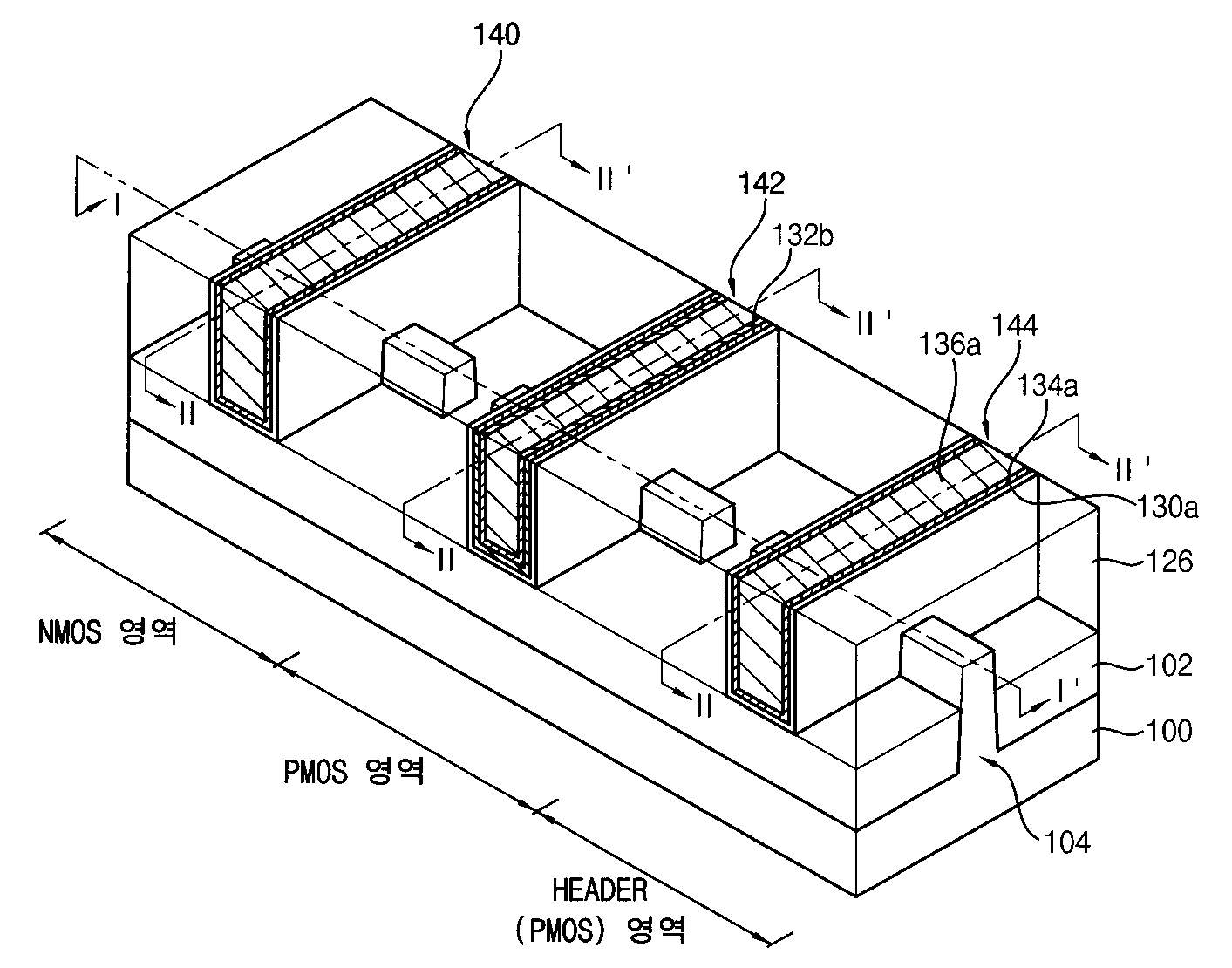
도 1 내지 도 3은 본 발명의 일 실시예에 따른 반도체 소자를 나타내는 사시도 및 단면도들이다. 도 4는 반도체 소자에서 각 트랜지스터의 배치를 나타낸다. 도 2 및 도 3은 각각 도 1의 I-I' 및 II-II' 선을 절단한 단면도들이다. 1 to 3 are perspective and cross-sectional views illustrating a semiconductor device according to an embodiment of the present invention. 4 shows the arrangement of each transistor in the semiconductor device. 2 and 3 are cross-sectional views taken along lines II' and II-II' of FIG. 1, respectively.
도 4를 참조하면, 반도체 소자의 로직 영역(10) 내에는 로직 회로들을 구성하는 NMOS 및 PMOS 트랜지스터들이 구비된다. 상기 로직 회로의 입력단에는 상기 로직 회로들의 입력부를 스위칭하는 해더 트랜지스터가 연결될 수 있다. 상기 해더 트랜지스터는 상기 반도체 소자의 전원 전압(Vdd)과 연결될 수 있다. 한편, 상기 로직 회로의 출력단에는 상기 로직 회로들의 출력부를 스위칭하는 풋터 트랜지스터가 연결될 수 있다. 일반적으로, 상기 반도체 소자에는 해더 트랜지스터와 풋터 트랜지스터 중 어느 하나만 구비될 수 있다. Referring to FIG. 4 , NMOS and PMOS transistors constituting logic circuits are provided in the
상기 해더 트랜지스터는 PMOS 트랜지스터가 주로 사용되며, 상기 로직 회로들을 구성하는 NMOS 및 PMOS 트랜지스터에 비해 높은 문턱 전압을 가질 수 있다. 또한, 상기 해더 트랜지스터는 낮은 대기 전류 및 누설 전류를 가져야 한다. 상기 풋터 트랜지스터는 NMOS 트랜지스터가 주로 사용되며, 상기 로직 회로들을 구성하는 NMOS 및 PMOS 트랜지스터에 비해 높은 문턱 전압을 가질 수 있다. 또한, 상기 풋터 트랜지스터는 낮은 대기 전류 및 누설 전류를 가져야 한다.As the header transistor, a PMOS transistor is mainly used, and may have a higher threshold voltage than the NMOS and PMOS transistors constituting the logic circuits. In addition, the header transistor should have low quiescent current and leakage current. An NMOS transistor is mainly used as the foot transistor, and may have a higher threshold voltage than NMOS and PMOS transistors constituting the logic circuits. In addition, the foot transistor should have low quiescent current and leakage current.
도 1 내지 도 3에서는 해더 트랜지스터를 포함하는 반도체 소자에 대해 설명한다. A semiconductor device including a header transistor will be described with reference to FIGS. 1 to 3 .
도 1 내지 도 3을 참조하면, 해더 영역, NMOS 영역 및 PMOS 영역이 포함되는 기판(100)이 구비된다. 상기 해더 영역에는 해더 트랜지스터로 제공되는 제1 트랜지스터가 형성되고, NMOS영역에는 로직 회로들을 구성하는 제2 트랜지스터가 형성되고 상기 PMOS영역에는 로직 회로들을 구성하는 제3 트랜지스터들이 형성될 수 있다. 상기 제1 트랜지스터는 P형 트랜지스터이고, 상기 제2 트랜지스터들은 NMOS 트랜지스터일 수 있고, 상기 제3 트랜지스터들은 PMOS트랜지스터일 수 있다. 1 to 3 , a
상기 기판(100)은 예를 들어, 실리콘 기판, 게르마늄 기판, 실리콘-게르마늄 기판, 실리콘 온 인슐레이터(Silicon-On-Insulator: SOI) 기판, 게르마늄 온 인슐레이터(Germanium-On-Insulator: GOI) 기판 등을 포함할 수 있다.The
상기 기판(100)에는 소자 분리막(102) 및 상기 소자 분리막(102)으로부터 돌출되는 액티브 핀들(104)이 구비될 수 있다.The
상기 소자 분리막(102)은 실리콘 산화물을 포함할 수 있다. 상기 액티브 핀들(104)은 상기 기판(100)을 식각하여 형성할 수 있으며, 이 경우 상기 액티브 핀들(104)과 기판(100)은 실질적으로 동일한 물질일 수 있다. The
상기 제1 트랜지스터는 제1 게이트 구조물(140), 제1 채널 영역(106) 및 제1 소스/드레인 영역(120)을 포함할 수 있다. The first transistor may include a
상기 제1 게이트 구조물(140)은 상기 해더 영역의 액티브 핀(104) 상에 구비될 수 있다. 상기 제1 게이트 구조물(140)은 산화막 패턴(128), 고유전막 패턴(130a), 제1 N형 금속 패턴(134a) 및 게이트 패턴(136a)을 포함한다. 상기 제1 채널 영역(106)은 상기 제1 게이트 구조물(140)의 저면과 대향하는 상기 액티브 핀(104)에 구비될 수 있다. 상기 제1 채널 영역(106)은 N형 불순물이 도핑된 영역일 수 있다. 또한, 상기 제1 소스/드레인 영역(120)은 상기 제1 게이트 구조물(140) 양 측의 액티브 핀(104)에 P형 불순물이 도핑되어 형성될 수 있다. 상기 제1 트랜지스터에서 상기 고유전막 패턴(130a)과 접촉하는 금속 패턴은 상기 제1 채널 영역(106)의 도전형과 동일하게 N형을 가질 수 있다. The
상기 산화막 패턴(128)은 열산화 공정을 통해 형성된 실리콘 산화물을 포함할 수 있다. 상기 고유전막 패턴은 실리콘 질화물보다 높은 유전율을 갖는 금속 산화물을 포함할 수 있다. 상기 고유전막 패턴은 예를들어, 하프늄 산화물(HfO2), 탄탈륨 산화물(Ta2O5), 지르코늄 산화물(ZrO2) 등을 포함할 수 있다. The
상기 제1 N형 금속 패턴(134a)은 페르미 레벨이 실리콘의 컨덕션 밴드와 가깝게 위치하는 금속 물질을 포함하고, 즉 일함수가 약 4.5eV 이하인 금속 물질을 포함할 수 있다. 상기 제1 N형 금속 패턴(134a)은 예를들어 티타늄(Ti), 은(Ag), 알루미늄(Al), TiAl, AiAlN, TaC, TaCN, TaSiaN, Mn, Zr등을 포함할 수 있다.The first N-
상기 게이트 패턴(136a)은 저저항의 금속 물질을 포함할 수 있다. 상기 게이트 패턴(136a)은 예를들어, 알루미늄(Al), 구리(Cu), 탄탈륨(Ta) 등을 포함할 수 있다.The
상기 제2 트랜지스터는 상기 제2 게이트 구조물(142), 제2 채널 영역(108) 및 제2 소스/드레인 영역(122)을 포함할 수 있다.The second transistor may include the
상기 제2 게이트 구조물(142)은 상기 NMOS 영역의 액티브 핀(104) 상에 구비될 수 있다. 상기 제2 게이트 구조물(142)은 상기 산화막 패턴(128), 고유전막 패턴(130a), 제1 N형 금속 패턴(134a) 및 게이트 패턴(136a)을 포함한다. 즉, 상기 제1 및 제2 게이트 구조물(140, 142)은 실질적으로 동일한 적층 구조를 가질 수 있다. 상기 제2 채널 영역(108)은 상기 제2 게이트 구조물(142)의 저면과 대향하는 상기 액티브 핀(104)에 구비될 수 있다. 상기 제2 채널 영역(108)은 P형 불순물이 도핑된 영역일 수 있다. 또한, 상기 제2 소스/드레인 영역(122)은 상기 제2 게이트 구조물(142) 양 측의 액티브 핀(104)에 N형 불순물이 도핑되어 형성될 수 있다. 상기 제2 트랜지스터에서 상기 고유전막 패턴(130a)과 접촉하는 금속 패턴은 상기 제2 채널 영역(108)의 도전형과 다른 N형을 가질 수 있다. The
예시적인 실시예에 있어서, 상기 제2 게이트 구조물(142) 양 측의 액티브 핀에는 제1 개구부가 구비될 수 있고, 상기 제1 개구부 내부에는 제1 반도체 패턴이 구비될 수 있다. 상기 제1 반도체 패턴은 에피택셜 성장 공정을 통해 형성된 실리콘일 수 있다. 또한, 상기 제2 소스/드레인 영역(122)은 상기 제1 반도체 패턴 내에 형성될 수 있다. In an exemplary embodiment, a first opening may be provided in the active fin on both sides of the
상기 제3 트랜지스터는 상기 제3 게이트 구조물(144), 제3 채널 영역(110) 및 제3 소스/드레인 영역(124)을 포함할 수 있다. The third transistor may include the
상기 제3 게이트 구조물(144)은 상기 PMOS 영역의 액티브 핀 상에 구비될 수 있다. 상기 제3 게이트 구조물(144)은 상기 산화막 패턴(128), 고유전막 패턴(130a), 상기 제1 P형 금속 패턴(132b), 상기 제1 N형 금속 패턴(134a) 및 게이트 패턴(136a)을 포함한다. 즉, 상기 제1 및 제3 게이트 구조물(140, 144)은 서로 다른 적층 구조를 가질 수 있다. 상기 제3 채널 영역(110)은 상기 제3 게이트 구조물(144)의 저면과 대향하는 상기 액티브 핀(104)에 구비될 수 있다. 상기 제3 채널 영역(110)은 N형 불순물이 도핑된 영역일 수 있다. 또한, 상기 제3 소스/드레인 영역(124)은 상기 제3 게이트 구조물(144) 양 측의 액티브 핀에 P형 불순물이 도핑되어 형성될 수 있다. 상기 제3 트랜지스터에서 상기 고유전막 패턴(130a)과 접촉하는 금속 패턴(132b)은 상기 제3 채널 영역(110)의 도전형과 다른 P형을 가질 수 있다. The
상기 제1 P형 금속 패턴(132b)은 페르미 레벨이 실리콘의 밸런스 밴드와 가깝게 위치하는 금속 물질이고, 즉 일함수가 약 4.5eV 이상인 금속 물질을 포함할 수 있다. 상기 제1 P형 금속 패턴(132b)은 예를들어 티타늄 질화물(TiN), 텅스텐 질화물(WN), 탄탈륨 질화물(TaN), 루테늄(Ru) 등을 포함할 수 있다.The first P-
예시적인 실시예에 있어서, 상기 제3 게이트 구조물(144) 양 측의 액티브 핀(104)에는 제2 개구부가 구비될 수 있고, 상기 제2 개구부 내부에는 제2 반도체 패턴이 구비될 수 있다. 상기 제2 반도체 패턴은 에피택셜 성장 공정을 통해 형성된 실리콘 게르마늄일 수 있다. 또한, 상기 제3 소스/드레인 영역(124)은 상기 제2 반도체 패턴 내에 형성될 수 있다. In an exemplary embodiment, a second opening may be provided in the
상기 제1 및 제3 트랜지스터는 P형의 도전형을 갖지만, 상기 제1 및 제3 게이트 구조물은 서로 다른 적층 구조를 가질 수 있다. 즉, 해더 트랜지스터와 로직 회로의 PMOS 트랜지스터는 서로 다른 게이트 구조 적층 구조를 가질 수 있다. The first and third transistors may have a P-type conductivity, but the first and third gate structures may have different stacked structures. That is, the header transistor and the PMOS transistor of the logic circuit may have different stacked gate structures.
상기 제1 트랜지스터와 같이, 상기 고유전막 패턴(130a)과 직접 접촉되는 금속 패턴의 도전형과 채널 영역의 도전형을 동일하게 함으로써, 트랜지스터의 문턱 전압을 상승시킬 수 있다. 즉, 상기 제1 트랜지스터의 문턱 전압의 절대값은 상기 제3 트랜지스터의 문턱 전압의 절대값보다 더 높을 수 있다.Like the first transistor, the threshold voltage of the transistor may be increased by making the conductivity type of the metal pattern in direct contact with the high-
상기 제1 내지 제3 트랜지스터는 액티브 핀 상에 형성되는 핀형 트랜지스터들일 수 있다. 상기 제1 내지 제3 게이트 구조물(140, 142, 144)의 선폭은 50㎚이하일 수 있다. 따라서, 상기 제1 내지 제3 트랜지스터는 게이트 길이가 각각 50㎚이하일 수 있다.The first to third transistors may be fin-type transistors formed on an active fin. A line width of the first to
상기 제1 트랜지스터가 핀형 트랜지스터가 아니라 플레너형 트랜지스터인 경우에, 상기 고유전막 패턴(130a)과 직접 접촉되는 금속 패턴의 도전형과 채널 영역의 도전형을 동일하게 형성하면 상기 트랜지스터의 문턱 전압이 전원 전압 이상으로 과도하게 높아질 수 있다. 따라서, 상기 플레너형의 트랜지스터는 스위치의 역할을 하기가 어려울 수 있다. 또한, 상기 제1 트랜지스터의 게이트 길이가 50㎚이상인 경우에는 상기 제1 트랜지스터가 차지하는 수평 면적이 증가되어 집적도를 높이기 어려울 수 있다. When the first transistor is a planar transistor rather than a pin-type transistor, if the conductivity type of the metal pattern directly in contact with the high-
그러나, 본 발명의 일 실시예에서, 상기 제1 및 제3 트랜지스터가 각각 핀형 트랜지스터이고, 게이트 길이가 50㎚이하일 수 있다. 그러므로, 상기 제1 및 제3 트랜지스터의 문턱 전압의 차이가 0.4V 이내가 될 수 있다. 따라서, 상기 제1 트랜지스터의 문턱 전압의 절대값은 전원 전압보다 낮을 수 있어서, 상기 제1 트랜지스터는 해더 트랜지스터로 동작할 수 있다. However, in an embodiment of the present invention, each of the first and third transistors is a fin-type transistor, and the gate length may be 50 nm or less. Therefore, a difference between the threshold voltages of the first and third transistors may be within 0.4V. Accordingly, the absolute value of the threshold voltage of the first transistor may be lower than the power supply voltage, so that the first transistor may operate as a header transistor.
예를들어, 상기 제1 트랜지스터의 문턱 전압의 절대값은 상기 제3 트랜지스터의 문턱 전압의 절대값보다 0.2 내지 0.4V 정도 높을 수 있다. 이 때, 상기 제1 트랜지스터의 문턱 전압의 절대값은 1.5V 보다 낮을 수 있다. 따라서, 상기 제1 트랜지스터는 전원전압이 1.5V 이하인 반도체 소자에서 해더 트랜지스터로 사용될 수 있다. For example, the absolute value of the threshold voltage of the first transistor may be 0.2 to 0.4V higher than the absolute value of the threshold voltage of the third transistor. In this case, the absolute value of the threshold voltage of the first transistor may be lower than 1.5V. Accordingly, the first transistor may be used as a header transistor in a semiconductor device having a power supply voltage of 1.5V or less.
도 5 내지 도 22는 도 1 내지 도 3에 도시된 반도체 소자의 제조 방법을 나타내는 사시도 및 단면도들이다. 5 to 22 are perspective and cross-sectional views illustrating a method of manufacturing the semiconductor device illustrated in FIGS. 1 to 3 .
도 5 내지 7을 참조하면, 기판(100) 상부를 부분적으로 식각하여 트렌치들을 형성하고, 트렌치들 하부를 채우는 소자 분리막(102)을 형성한다. 5 to 7 , the upper portion of the
상기 기판(100)은 해더 트랜지스터가 형성되는 해더 영역과, 로직 회로들을 구성하는 NMOS 및 PMOS 트랜지스터들이 형성되는 NMOS 영역 및 PMOS 영역을 각각 포함할 수 있다. 상기 기판(100)은 예를 들어, 실리콘 기판, 게르마늄 기판, 실리콘-게르마늄 기판, 실리콘 온 인슐레이터(Silicon-On-Insulator: SOI) 기판, 게르마늄 온 인슐레이터(Germanium-On-Insulator: GOI) 기판 등을 포함할 수 있다.The
상기 소자 분리막(102)을 형성하기 위하여, 상기 트렌치들을 충분히 채우는 절연막을 상기 기판(100) 상에 형성하고, 상기 기판(100) 상면이 노출될 때까지 상기 절연막을 평탄화한다. 다음에, 상기 트렌치들의 상부 측벽이 노출되도록 상기 절연막 상부를 제거한다. 상기 절연막은, 예를 들어, 실리콘 산화물과 같은 산화물을 포함할 수 있다. In order to form the
따라서, 상기 기판(100)에는 소자 분리막(102) 및 상기 소자 분리막(102)으로부터 돌출되는 액티브 핀들(active fin, 104)이 형성될 수 있다. Accordingly, the
도 8 및 9를 참조하면, 상기 해더 영역, NMOS 영역 및 PMOS 영역에 형성된 액티브 핀들(104) 표면에 각각 불순물들을 이온 주입하여 제1 내지 제3 채널 영역들(106, 108, 110)을 각각 형성할 수 있다. 8 and 9 , first to
상기 해더 영역 및 PMOS 영역에는 PMOS 트랜지스터가 형성된다. 그러므로, 상기 해더 영역 및 PMOS 영역의 액티브 핀들(104)에는 N형 불순물을 주입하여 제1 및 제3 채널 영역들(106, 110)을 각각 형성할 수 있다. 또한, 상기 NMOS 영역에는 NMOS 트랜지스터가 형성된다. 그러므로, 상기 NMOS 영역의 액티브 핀(104)에는 P형 불순물을 주입하여 제2 채널 영역(108)을 형성할 수 있다. A PMOS transistor is formed in the header region and the PMOS region. Therefore, N-type impurities may be implanted into the
도 10 및 11을 참조하면, 상기 해더 영역, NMOS 영역 및 PMOS 영역의 액티브 핀들(104) 상에 각각 제1 내지 제3 더미 게이트 구조물(116a, 116b, 116c)을 형성할 수 있다. 10 and 11 , first to third
구체적으로, 상기 기판(10) 상에 더미 게이트 절연막 및 더미 게이트 전극막을 형성할 수 있다. 상기 더미 게이트 전극막 상에 마스크 패턴들을 형성하고, 상기 마스크 패턴들을 이용하여 상기 더미 게이트 전극막 및 게이트 절연막을 식각하여 상기 제1 내지 제3 더미 게이트 구조물(116a, 116b, 116c)을 형성할 수 있다. 상기 제1 내지 제3 더미 게이트 구조물(116a, 116b, 116c)은 더미 게이트 절연막 패턴(112) 및 더미 게이트 전극(114)을 포함할 수 있다. 도시하지는 않았지만, 상기 더미 게이트 전극(114) 상에는 상기 마스크 패턴이 남아있을 수도 있다.Specifically, a dummy gate insulating layer and a dummy gate electrode layer may be formed on the
상기 더미 게이트 절연막은 예를 들어, 실리콘 산화물과 같은 산화물을 포함하도록 형성될 수 있고, 상기 더미 게이트 전극막은 예를 들어, 폴리실리콘을 포함하도록 형성될 수 있다. 또한, 상기 마스크 패턴은 예를들어, 실리콘 질화물과 같은 질화물을 포함하도록 형성될 수 있다. The dummy gate insulating layer may be formed to include, for example, an oxide such as silicon oxide, and the dummy gate electrode layer may be formed to include, for example, polysilicon. In addition, the mask pattern may be formed to include, for example, a nitride such as silicon nitride.
상기 제1 내지 제3 더미 게이트 구조물(116a, 116b, 116c)의 선폭은 각각 50㎚이하일 수 있다.Each of the first to third
상기 제1 내지 제3 더미 게이트 구조물(116a, 116b, 116c)의 측벽에 스페이서(118)를 형성할 수 있다. 상기 스페이서(118)는 상기 제1 내지 제3 더미 게이트 구조물(116a, 116b, 116c) 및 기판(100) 표면 상에 스페이서막을 형성하고, 상기 스페이서막을 이방성 식각함으로써 형성될 수 있다.
도 12를 참조하면, 상기 NMOS 영역 및 PMOS 영역의 액티브 핀들(104) 부위에 에피택셜 성장 공정을 수행하여 제1 및 제2 반도체 패턴을 각각 형성한다. Referring to FIG. 12 , an epitaxial growth process is performed on the
구체적으로, 상기 NMOS 영역에 형성된 상기 제2 더미 게이트 구조물 (116b) 양 측의 액티브 핀을 식각하여 제1 개구부를 형성하고, 상기 제1 개구부에 실리콘을 에피택셜 성장시켜 제1 반도체 패턴을 형성한다. Specifically, a first opening is formed by etching the active fins on both sides of the second
상기 PMOS 영역에 형성된 상기 제3 더미 게이트 구조물 양 측의 액티브 핀을 식각하여 제2 개구부를 형성하고, 상기 제2 개구부에 실리콘 게르마늄을 에피택셜 성장시켜 제2 반도체 패턴을 형성한다. 상기 제1 및 제2 반도체 패턴이 형성됨에 따라 상기 채널 영역에 스트레스가 가해지게 되고, 이로인해 NMOS 트랜지스터 및 PMOS 트랜지스터의 전하 이동도가 향상될 수 있다.A second opening is formed by etching the active fins on both sides of the third dummy gate structure formed in the PMOS region, and silicon germanium is epitaxially grown in the second opening to form a second semiconductor pattern. As the first and second semiconductor patterns are formed, stress is applied to the channel region, and thus charge mobility of the NMOS transistor and the PMOS transistor may be improved.
다음에, 상기 제1 내지 제3 더미 게이트 구조물(116a, 116b, 116c)의 양 측에 각각 불순물들을 도핑하여, 제1 내지 제3 소스/드레인 영역들(120, 122, 124)을 각각 형성할 수 있다.Next, the first to third
구체적으로, 상기 해더 영역 및 PMOS 영역에는 각각 P형 불순물을 주입한다. 따라서, 상기 제1 더미 게이트 구조물(116a) 양 측의 액티브 핀(104)과 상기 제2 반도체 패턴 내부에 각각 제1 및 제3 소스/드레인 영역들(120, 124)을 형성할 수 있다. 또한, 상기 NMOS 영역에는 N형 불순물을 주입한다. 따라서, 상기 제1 반도체 패턴 내부에 제2 소스/드레인 영역들(122)을 형성할 수 있다. Specifically, P-type impurities are implanted into the header region and the PMOS region, respectively. Accordingly, first and third source/
도 13 및 도 14를 참조하면, 상기 제1 내지 제3 더미 게이트 구조물(116a, 116b, 116c)을 덮도록 층간 절연막(126)을 충분한 높이로 형성한다. 이 후, 상기 제1 내지 제3 더미 게이트 구조물(116a, 116b, 116c)의 상부면이 노출되도록 상기 층간 절연막(126)을 평탄화시킨다. 상기 평탄화 공정은 화학 기계적 연마(Chemical Mechanical Polishing: CMP) 공정 및/또는 에치 백(etch back) 공정에 의해 수행될 수 있다.13 and 14 , an
상기 제1 내지 제3 더미 게이트 구조물(116a, 116b, 116c)을 제거하여, 상기 층간 절연막(126) 내에 개구부들(127)을 형성한다. 상기 식각 공정에서, 상기 개구부들(127) 저면에 상기 액티브 핀(104)의 표면이 노출되도록 할 수 있다.The first to third
상기 개구부(127) 저면에 노출된 상기 액티브 핀(104) 상에 산화막 패턴(128)을 형성한다. 상기 산화막 패턴(128)은 열산화 공정을 통해 형성된 실리콘 산화물을 포함할 수 있다. 상기 산화막 패턴(128)은 예를들어, 오존 가스를 사용하여 상기 액티브 핀(104) 표면을 산화시킴으로써 형성할 수 있다.An
상기 개구부(127) 측벽, 산화막 패턴(128) 및 층간 절연막(126) 상부면 상에 컨포멀하게 고유전막(130)을 형성한다. 상기 고유전막(130)은 실리콘 질화물보다 높은 유전율을 갖는 금속 산화물을 포함할 수 있다. 상기 고유전막(130)은, 예를 들어, 하프늄 산화물(HfO2), 탄탈륨 산화물(Ta2O5), 지르코늄 산화물(ZrO2) 등을 포함할 수 있다. A
도 15 및 도 16을 참조하면, 상기 고유전막(130) 상에 컨포멀하게 제1 P형 금속막(132)을 형성한다. 상기 제1 P형 금속막(132)은 페르미 레벨이 실리콘의 밸런스 밴드와 가깝게 위치하는 금속 물질이고, 즉 일함수가 약 4.5eV 이상인 금속 물질을 포함할 수 있다. 상기 제1 P형 금속막(132)은 예를들어 티타늄 질화물(TiN), 텅스텐 질화물(WN), 탄탈륨 질화물(TaN), 루테늄(Ru) 등을 포함할 수 있다.15 and 16 , a first P-
도 17 및 도 18을 참조하면, 상기 제1 P형 금속막(132)의 일부를 식각하여 상기 PMOS 영역에 형성된 상기 고유전막(130) 상에 예비 제1 P형 금속 패턴(132a)을 형성한다. 17 and 18 , a portion of the first P-
구체적으로, 상기 제1 P형 금속막(132) 상에 사진 공정을 수행하여 포토레지스트 패턴(133)을 형성한다. 상기 포토레지스트 패턴(133)은 상기 PMOS영역에 형성된 상기 제1 P형 금속막(132)을 선택적으로 덮는 형상을 가질 수 있다. 상기 포토레지스트 패턴(133)을 이용하여, 상기 NMOS 영역 및 해더 영역에 형성된 제1 P형 금속막(132)을 제거한다. 따라서, 상기 NMOS 영역 및 해더 영역에는 상기 고유전막(130)이 노출될 수 있다. Specifically, a
도 19 및 도 20을 참조하면, 상기 고유전막(130) 및 상기 예비 제1 P형 금속 패턴(132a) 상에 컨포멀하게 제1 N형 금속막(134)을 형성한다. 따라서, 상기 NMOS 영역 및 해더 영역의 고유전막(130) 상에는 상기 제1 N형 금속막(134)이 직접 접촉되고, 상기 PMOS 영역의 고유전막(130) 상에는 상기 예비 제1 P형 금속 패턴(132a)이 직접 접촉된다. 19 and 20 , a first N-
상기 제1 N형 금속막(134)은 페르미 레벨이 실리콘의 컨덕션 밴드와 가깝게 위치하는 금속 물질이고, 즉 일함수가 약 4.5eV 이하인 금속 물질을 포함할 수 있다. 상기 제1 N형 금속막(134)은 예를들어 티타늄(Ti), 은(Ag), 알루미늄(Al), TiAl, AiAlN, TaC, TaCN, TaSiaN, Mn, Zr등을 포함할 수 있다.The first N-
도 21 및 도 22를 참조하면, 상기 제1 N형 금속막(134) 상에 상기 개구부들(127) 내부를 채우도록 게이트 전극막(136)을 형성한다. 상기 게이트 전극막(136)은 저저항의 금속 물질을 포함할 수 있다. 상기 게이트 전극막(136)은 예를들어, 알루미늄(Al), 구리(Cu), 탄탈륨(Ta) 등의 금속을 포함할 수 있다.21 and 22 , a
다시, 도 1 내지 도 3을 참조하면, 상기 층간 절연막(126)의 상부면이 노출될 때까지, 상기 게이트 전극막(136), 제1 N형 금속막(134), 예비 제1 P형 금속 패턴(132a) 및 고유전막(130)을 평탄화한다. 상기 공정들을 통해 해더 영역, NMOS 영역 및 PMOS 영역에는 각각 제1 내지 제3 게이트 구조물(140, 142, 144)이 형성된다.Again, referring to FIGS. 1 to 3 , the
상기 제1 내지 제3 게이트 구조물(140, 142, 144)은 상기 제1 내지 제3 더미 게이트 구조물(116a, 116b, 116c)이 제거된 부위에 각각 형성된다. 그러므로, 상기 제1 내지 제3 게이트 구조물(140, 142, 144)의 선폭은 각각 50㎚이하일 수 있다. 따라서, 상기 제1 내지 제3 게이트 구조물(140, 142, 144)을 포함하는 제1 내지 제3 트랜지스터는 50㎚이하의 게이트 길이를 가질 수 있다. The first to
상기 제1 게이트 구조물(140)은 산화막 패턴(128), 고유전막 패턴(130a), 제1 N형 금속 패턴(134a) 및 게이트 패턴(136a)을 포함한다. 상기 제2 게이트 구조물(142)은 산화막 패턴(128), 고유전막 패턴(130a), 제1 N형 금속 패턴(134a) 및 게이트 패턴(136a)을 포함한다. 상기 제3 게이트 구조물(144)은 산화막 패턴(128), 고유전막 패턴(130a), 제1 P형 금속 패턴(132b), 제1 N형 금속 패턴(134a) 및 게이트 패턴(136a)을 포함한다. The
상기 공정에 의해, 상기 해더 영역 및 상기 PMOS 영역에는 P형의 제1 및 제3 트랜지스터가 각각 형성된다. 또한, 상기 NMOS 영역에는 N형의 제2 트랜지스터가 형성된다. Through the above process, first and third P-type transistors are respectively formed in the header region and the PMOS region. In addition, an N-type second transistor is formed in the NMOS region.
본 발명의 일 실시예에 의하면, 상기 제1 트랜지스터는 로직 회로들을 구성하는 트랜지스터들보다 높은 문턱 전압을 갖는 해더 트랜지스터로 제공된다. 상기 제1 트랜지스터를 형성하는 공정에서 문턱 전압 조절을 위한 할로 이온 주입과 같은 공정들이 수행되지 않는다. 또한, 상기 제1 트랜지스터를 형성하기 위한 추가적인 사진 공정이 요구되지 않는다. 그러므로, 별도의 추가 공정들을 수행하지 않으면서 목표 문턱 전압을 갖는 상기 해더 트랜지스터를 형성할 수 있다. According to an embodiment of the present invention, the first transistor is provided as a header transistor having a higher threshold voltage than transistors constituting the logic circuits. In the process of forming the first transistor, processes such as halo ion implantation for adjusting a threshold voltage are not performed. In addition, an additional photo process for forming the first transistor is not required. Therefore, it is possible to form the header transistor having a target threshold voltage without performing additional additional processes.
도 23 내지 도 25는 본 발명의 일 실시예에 따른 반도체 소자를 나타내는 사시도 및 단면도들이다. 도 24 및 도 25는 각각 도 23의 I-I' 및 II-II' 선을 절단한 단면도들이다.23 to 25 are perspective and cross-sectional views illustrating a semiconductor device according to an embodiment of the present invention. 24 and 25 are cross-sectional views taken along lines II' and II-II' of FIG. 23, respectively.
본 실시예에 따른 반도체 소자는 제1 내지 제3 트랜지스터에 포함되는 제1 내지 제3 게이트 구조물의 적층 구조를 제외하고는 도 1 내지 3을 참조로 설명한 것과 실질적으로 동일하다.The semiconductor device according to the present embodiment is substantially the same as described with reference to FIGS. 1 to 3 except for the stacked structure of the first to third gate structures included in the first to third transistors.
도 23 내지 도 25를 참조하면, 해더 영역, NMOS 영역 및 PMOS 영역이 포함되는 기판(100)이 구비된다. 상기 해더 영역에는 해더 트랜지스터로 제공되는 제1 트랜지스터가 형성되고, NMOS영역에는 로직 회로들을 구성하는 제2 트랜지스터가 형성되고 상기 PMOS영역에는 로직 회로들을 구성하는 제3 트랜지스터들이 형성될 수 있다. 상기 제1 트랜지스터는 P형 트랜지스터일 수 있고, 상기 제2 트랜지스터들은 NMOS 트랜지스터일 수 있고, 상기 제3 트랜지스터들은 PMOS트랜지스터일 수 있다. 23 to 25 , a
상기 기판(100)에는 소자 분리막(102) 및 상기 소자 분리막(102)으로부터 돌출되는 액티브 핀들(104)이 구비될 수 있다.The
상기 제1 트랜지스터는 상기 제1 게이트 구조물(140), 제1 채널 영역(106) 및 제1 소스/드레인 영역(120)을 포함할 수 있다. The first transistor may include the
상기 제1 게이트 구조물(140a)은 상기 해더 영역의 액티브 핀(104) 상에 구비될 수 있다. 상기 제1 게이트 구조물(140a)은 산화막 패턴(128), 고유전막 패턴(130a), 제1 N형 금속 패턴(150), 제1 P형 금속 패턴(152) 및 게이트 패턴(154)을 포함한다. 상기 제1 채널 영역에는 N형 불순물이 도핑되고, 상기 제1 소스/드레인 영역에는 P형 불순물이 도핑될 수 있다. The
상기 제1 트랜지스터에서 상기 고유전막 패턴(130a)과 접촉하는 금속 패턴(134a)은 상기 제1 채널 영역(106)의 도전형과 동일하게 N형을 가질 수 있다. 한편, 상기 제1 N형 금속 패턴 상에는 제1 P형 금속 패턴이 구비된다. 그러나, 상기 제1 P형 금속 패턴은 상기 고유전막 패턴과 접촉하지 않기 때문에 트랜지스터의 문턱 전압에 영향을 주지 않을 수 있다. In the first transistor, the
상기 제2 트랜지스터는 상기 제2 게이트 구조물(142a), 제2 채널 영역(108) 및 제2 소스/드레인 영역(122)을 포함할 수 있다. The second transistor may include the
상기 제2 게이트 구조물(142a)은 상기 NMOS 영역의 액티브 핀(104) 상에 구비될 수 있다. 상기 제2 게이트 구조물(142a)은 상기 산화막 패턴(128), 고유전막 패턴(130a), 제1 N형 금속 패턴(150), 제1 P형 금속 패턴(152) 및 게이트 패턴(154)을 포함한다. 즉, 상기 제1 및 제2 게이트 구조물(140a, 142a)은 동일한 적층 구조를 가질 수 있다. 상기 제2 채널 영역에는 P형 불순물이 도핑되고, 상기 제2 소스/드레인 영역에는 N형 불순물이 도핑될 수 있다. 상기 제2 트랜지스터에서 상기 고유전막 패턴(130a)과 접촉하는 금속 패턴은 상기 제2 채널 영역(108)의 도전형과 다른 N형을 가질 수 있다. The
예시적인 실시예에 있어서, 상기 제2 게이트 구조물(142a) 양 측의 액티브 핀에는 제1 개구부가 구비될 수 있고, 상기 제1 개구부 내부에는 제1 반도체 패턴이 구비될 수 있다. 상기 제2 소스/드레인 영역(122)은 상기 제1 반도체 패턴 내에 형성될 수 있다. In an exemplary embodiment, a first opening may be provided in the active fin on both sides of the
상기 제3 트랜지스터는 상기 제3 게이트 구조물(144a), 제3 채널 영역(110) 및 제3 소스/드레인 영역(124)을 포함할 수 있다. The third transistor may include the
상기 제3 게이트 구조물(144a)은 상기 PMOS 영역의 액티브 핀 상에 구비될 수 있다. 상기 제3 게이트 구조물(144a)은 상기 산화막 패턴(128), 고유전막 패턴(130a), 상기 제1 P형 금속 패턴(152) 및 게이트 패턴(136a)을 포함한다. 즉, 상기 제1 및 제3 게이트 구조물(140a, 144a)은 서로 다른 적층 구조를 가질 수 있다. 상기 제3 채널 영역에는 N형 불순물이 도핑되고, 상기 제3 소스/드레인 영역에는 P형 불순물이 도핑될 수 있다. The
본 발명의 일 실시예에 의하면, 상기 제1 트랜지스터는 로직 회로들을 구성하는 트랜지스터들보다 높은 문턱 전압을 갖는 해더 트랜지스터로 제공될 수 있다. According to an embodiment of the present invention, the first transistor may be provided as a header transistor having a higher threshold voltage than transistors constituting the logic circuits.
도 23 내지 도 25에 도시된 반도체 소자는 도 5 내지 도 22에서 설명한 것과 실질적으로 동일하거나 유사한 공정들을 수행하여 형성할 수 있다. 다만, 제1 내지 제3 게이트 구조물을 형성하기 위한 막의 적층 순서가 다를 수 있다.The semiconductor device illustrated in FIGS. 23 to 25 may be formed by performing processes substantially the same as or similar to those described in FIGS. 5 to 22 . However, the stacking order of layers for forming the first to third gate structures may be different.
먼저, 도 5 내지 도 14를 참조로 설명한 것과 실질적으로 동일한 공정을 수행한다. 이 후에, 상기 고유전막(130) 상에 컨포멀하게 제1 N형 금속막을 형성하고, 상기 제1 N형 금속막의 일부를 사진 식각 공정을 통해 제거하여 상기 NMOS 영역 및 해더 영역에 형성된 상기 고유전막(130) 상에 예비 제1 N형 금속 패턴을 형성한다. 계속하여, 상기 고유전막(130) 및 상기 예비 제1 N형 금속 패턴 상에 컨포멀하게 제1 P형 금속막을 형성하고, 개구부를 채우도록 게이트 전극막을 형성한다. First, substantially the same process as described with reference to FIGS. 5 to 14 is performed. Thereafter, a first N-type metal layer is conformally formed on the high-
다음에, 상기 층간 절연막(126)의 상부면이 노출될 때까지, 상기 게이트 전극막, 제1 P형 금속막, 예비 제1 N형 금속 패턴 및 고유전막(130)을 평탄화한다. 상기 공정들을 통해 해더 영역, NMOS 영역 및 PMOS 영역에는 각각 제1 내지 제3 게이트 구조물(140a, 142a, 144a)이 형성될 수 있다. Next, the gate electrode layer, the first P-type metal layer, the preliminary first N-type metal pattern, and the high-
본 발명의 일 실시예에 의하면, 상기 제1 트랜지스터를 형성하는 공정에서 문턱 전압 조절을 위한 할로 이온 주입과 같은 공정들이 수행되지 않는다. 또한, 상기 제1 트랜지스터를 형성하기 위한 추가적인 사진 공정이 요구되지 않는다. 그러므로, 별도의 추가 공정들을 수행하지 않으면서 상기 해더 트랜지스터를 형성할 수 있다. According to an embodiment of the present invention, in the process of forming the first transistor, processes such as halo ion implantation for adjusting a threshold voltage are not performed. In addition, an additional photo process for forming the first transistor is not required. Therefore, it is possible to form the header transistor without performing additional additional processes.
도 26 내지 도 28은 본 발명의 일 실시예에 따른 반도체 소자를 나타내는 사시도 및 단면도들이다. 도 27 및 도 28은 각각 도 26의 I-I' 및 II-II' 선을 절단한 단면도들이다.26 to 28 are perspective and cross-sectional views illustrating a semiconductor device according to an embodiment of the present invention. 27 and 28 are cross-sectional views taken along lines II' and II-II' of FIG. 26, respectively.
본 실시예에 따른 반도체 소자는 제1 트랜지스터가 풋터 트랜지스터로 제공된다. 본 실시예에 따른 반도체 소자는 상기 제1 트랜지스터를 제외하고는 도 1 내지 3을 참조로 설명한 것과 실질적으로 동일하다.In the semiconductor device according to the present embodiment, the first transistor is provided as a foot transistor. The semiconductor device according to the present embodiment is substantially the same as described with reference to FIGS. 1 to 3 except for the first transistor.
도 26 내지 도 28을 참조하면, 풋터 영역, NMOS 영역 및 PMOS 영역이 포함되는 기판(100)이 구비된다. 상기 풋터 영역에는 풋터 트랜지스터로 제공되는 제1 트랜지스터가 형성되고, NMOS영역에는 로직 회로들을 구성하는 제2 트랜지스터가 형성되고 상기 PMOS영역에는 로직 회로들을 구성하는 제3 트랜지스터들이 형성될 수 있다. 상기 제1 트랜지스터는 N형 트랜지스터일 수 있고, 상기 제2 트랜지스터들은 NMOS 트랜지스터일 수 있고, 상기 제3 트랜지스터들은 PMOS트랜지스터일 수 있다.26 to 28 , a
상기 기판(100)에는 소자 분리막(102) 및 상기 소자 분리막(102)으로부터 돌출되는 액티브 핀들(104)이 구비될 수 있다.The
상기 제1 트랜지스터는 상기 제1 게이트 구조물(200), 제1 채널 영역(106a) 및 제1 소스/드레인 영역(120a)을 포함할 수 있다. The first transistor may include the
상기 제1 게이트 구조물(200)은 상기 풋터 영역의 액티브 핀(104) 상에 구비될 수 있다. 상기 제1 게이트 구조물(200)은 산화막 패턴(128), 고유전막 패턴(130a), 제1 P형 금속 패턴(132b), 제1 N형 금속 패턴(134a) 및 게이트 패턴(136a)을 포함한다. 상기 제1 채널 영역(106a)에는 P형 불순물이 도핑되고, 상기 제1 소스/드레인 영역에는 N형 불순물이 도핑될 수 있다. The
상기 제1 트랜지스터에서 상기 고유전막 패턴(130a)과 접촉하는 금속 패턴(132b)은 상기 제1 채널 영역(106a)의 도전형과 동일하게 P형을 가질 수 있다. 한편, 상기 제1 P형 금속 패턴(132b) 상에는 제1 N형 금속 패턴(134a)이 구비된다. 그러나, 상기 제1 N형 금속 패턴(134a)은 상기 고유전막 패턴(130a)과 직접 접촉하지 않기 때문에 트랜지스터의 문턱 전압에 영향을 주지 않을 수 있다. In the first transistor, the
상기 제2 트랜지스터는 상기 제2 게이트 구조물(142), 제2 채널 영역(108) 및 제2 소스/드레인 영역(122)을 포함할 수 있다. The second transistor may include the
상기 제2 게이트 구조물(142)은 상기 NMOS 영역의 액티브 핀(104) 상에 구비될 수 있다. 상기 제2 게이트 구조물(142)은 상기 산화막 패턴(128), 고유전막 패턴(130a), 제1 N형 금속 패턴(134a) 및 게이트 패턴(136a)을 포함한다. 상기 제1 및 제2 트랜지스터는 동일한 도전형을 갖지만, 상기 제1 및 제2 게이트 구조물(200, 142)은 동일한 적층 구조를 갖지 않는다. 상기 제2 채널 영역(108)에는 P형 불순물이 도핑되고, 상기 제2 소스/드레인 영역(122)에는 N형 불순물이 도핑될 수 있다. The
상기 제2 트랜지스터에서 상기 고유전막 패턴(130a)과 접촉하는 금속 패턴은 상기 제2 채널 영역(108)의 도전형과 다른 N형을 가질 수 있다. In the second transistor, a metal pattern in contact with the high-
예시적인 실시예에 있어서, 상기 제2 소스/드레인 영역(122)은 제1 반도체 패턴 내에 형성될 수 있다. In an exemplary embodiment, the second source/
상기 제3 트랜지스터는 상기 제3 게이트 구조물(144), 제3 채널 영역(110) 및 제3 소스/드레인 영역(124)을 포함할 수 있다. The third transistor may include the
상기 제3 게이트 구조물(144)은 상기 PMOS 영역의 액티브 핀 상에 구비될 수 있다. 상기 제3 게이트 구조물(144)은 상기 산화막 패턴(128), 고유전막 패턴(130a), 상기 제1 P형 금속 패턴(132b), 제1 N형 금속 패턴(134a) 및 게이트 패턴(136a)을 포함한다. 즉, 상기 제1 및 제3 게이트 구조물(200, 144)은 서로 동일한 적층 구조를 가질 수 있다. 상기 제3 채널 영역에는 N형 불순물이 도핑되고, 상기 제3 소스/드레인 영역에는 P형 불순물이 도핑될 수 있다. The
예시적인 실시예에 있어서, 상기 제3 소스/드레인 영역(124)은 제2 반도체 패턴 내에 형성될 수 있다. In an exemplary embodiment, the third source/
본 발명의 일 실시예에 의하면, 상기 제1 트랜지스터는 로직 회로들을 구성하는 트랜지스터들보다 높은 문턱 전압을 갖는 풋터 트랜지스터로 제공될 수 있다. According to an embodiment of the present invention, the first transistor may be provided as a foot transistor having a higher threshold voltage than transistors constituting the logic circuits.
도 26 내지 도 28에 도시된 반도체 소자는 도 5 내지 도 22에서 설명한 것과 실질적으로 동일한 공정들을 수행하여 형성할 수 있다. 다만, 제1 내지 제3 게이트 구조물을 형성하기 위한 공정에서 제거되는 막에서만 차이가 있다. The semiconductor device shown in FIGS. 26 to 28 may be formed by performing substantially the same processes as those described with reference to FIGS. 5 to 22 . However, there is a difference only in the layer removed in the process for forming the first to third gate structures.
풋터 트랜지스터가 형성되는 풋터 영역과, 로직 회로들을 구성하는 NMOS 및 PMOS 트랜지스터들이 형성되는 NMOS 영역 및 PMOS 영역을 각각 포함하는 기판에, 도 5 내지 도 16을 참조로 설명한 것과 동일한 공정을 수행한다. 이 후에, 상기 제1 P형 금속막(132)의 일부를 사진 식각 공정을 통해 제거하여 상기 PMOS 영역 및 상기 풋터 영역에 형성된 상기 고유전막(130) 상에 예비 제1 P형 금속 패턴을 형성한다. 다음에, 도 19 내지 도 22를 참조로 설명한 공정들을 동일하게 수행하여 풋터 영역, NMOS 영역 및 PMOS 영역에 각각 제1 내지 제3 게이트 구조물(200, 142, 144)을 형성할 수 있다. The same process as described with reference to FIGS. 5 to 16 is performed on a substrate including a foot region in which a foot transistor is formed, and an NMOS region and a PMOS region in which NMOS and PMOS transistors constituting logic circuits are formed, respectively. Thereafter, a portion of the first P-
본 발명의 일 실시예에 의하면, 상기 제1 트랜지스터를 형성하는 공정에서 문턱 전압 조절을 위한 할로 이온 주입과 같은 공정들이 수행되지 않는다. 또한, 상기 제1 트랜지스터를 형성하기 위한 추가적인 사진 공정이 요구되지 않는다. 그러므로, 별도의 추가 공정들을 수행하지 않으면서 상기 풋터 트랜지스터를 형성할 수 있다. According to an embodiment of the present invention, in the process of forming the first transistor, processes such as halo ion implantation for adjusting a threshold voltage are not performed. In addition, an additional photo process for forming the first transistor is not required. Therefore, it is possible to form the foot transistor without performing additional additional processes.
도 29 내지 도 31은 본 발명의 일 실시예에 따른 반도체 소자를 나타내는 사시도 및 단면도들이다. 도 30 및 도 31은 각각 도 29의 I-I' 및 II-II' 선을 절단한 단면도들이다.29 to 31 are perspective and cross-sectional views illustrating a semiconductor device according to an embodiment of the present invention. 30 and 31 are cross-sectional views taken along lines II' and II-II' of FIG. 29, respectively.
본 실시예에 따른 반도체 소자는 제1 트랜지스터가 풋터 트랜지스터로 제공된다. 본 실시예에 따른 반도체 소자는 상기 제1 트랜지스터를 제외하고는 도 23 내지 25를 참조로 설명한 것과 실질적으로 동일하다.In the semiconductor device according to the present embodiment, the first transistor is provided as a foot transistor. The semiconductor device according to the present embodiment is substantially the same as described with reference to FIGS. 23 to 25 except for the first transistor.
도 29 내지 도 31을 참조하면, 풋터 영역, NMOS 영역 및 PMOS 영역이 포함되는 기판(100)이 구비된다. 상기 풋터 영역에는 풋터 트랜지스터로 제공되는 제1 트랜지스터가 형성되고, NMOS영역에는 로직 회로들을 구성하는 제2 트랜지스터가 형성되고 상기 PMOS영역에는 로직 회로들을 구성하는 제3 트랜지스터들이 형성될 수 있다. 상기 제1 트랜지스터는 N형 트랜지스터일 수 있고, 상기 제2 트랜지스터들은 NMOS 트랜지스터일 수 있고, 상기 제3 트랜지스터들은 PMOS트랜지스터일 수 있다.29 to 31 , a
상기 기판(100)에는 소자 분리막(102) 및 상기 소자 분리막(102)으로부터 돌출되는 액티브 핀들(104)이 구비될 수 있다.The
상기 제1 트랜지스터는 상기 제1 게이트 구조물(200a), 제1 채널 영역(106a) 및 제1 소스/드레인 영역(120a)을 포함할 수 있다. The first transistor may include the
상기 제1 게이트 구조물(200a)은 상기 풋터 영역의 액티브 핀(104) 상에 구비될 수 있다. 상기 제1 게이트 구조물(200a)은 산화막 패턴(128), 고유전막 패턴(130a), 제1 P형 금속 패턴(152) 및 게이트 패턴(154)을 포함한다. 상기 제1 채널 영역(106a)에는 P형 불순물이 도핑되고, 상기 제1 소스/드레인 영역에는 N형 불순물이 도핑될 수 있다. The
상기 제1 트랜지스터에서 상기 고유전막 패턴(130a)과 접촉하는 금속 패턴은 상기 제1 채널 영역(106a)의 도전형과 동일하게 P형을 가질 수 있다. In the first transistor, a metal pattern in contact with the high-
상기 제2 트랜지스터는 상기 제2 게이트 구조물(142a), 제2 채널 영역(108) 및 제2 소스/드레인 영역(122)을 포함할 수 있다. The second transistor may include the
상기 제2 게이트 구조물(142a)은 상기 NMOS 영역의 액티브 핀(104) 상에 구비될 수 있다. 상기 제2 게이트 구조물(142a)은 상기 산화막 패턴(128), 고유전막 패턴(130a), 제1 N형 금속 패턴(150), 제1 P형 금속 패턴(152) 및 게이트 패턴(154)을 포함한다. 상기 제1 및 제2 트랜지스터는 동일한 도전형을 갖지만, 상기 제1 및 제2 게이트 구조물(200a, 142a)은 동일한 적층 구조를 갖지 않는다. 상기 제2 채널 영역(108)에는 P형 불순물이 도핑되고, 상기 제2 소스/드레인 영역(122)에는 N형 불순물이 도핑될 수 있다. The
상기 제2 트랜지스터에서 상기 고유전막 패턴(130a)과 접촉하는 금속 패턴은 상기 제2 채널 영역(108)의 도전형과 다른 N형을 가질 수 있다. In the second transistor, a metal pattern in contact with the high-
예시적인 실시예에 있어서, 상기 제2 소스/드레인 영역(122)은 제1 반도체 패턴 내에 형성될 수 있다. In an exemplary embodiment, the second source/
상기 제3 트랜지스터는 상기 제3 게이트 구조물(144a), 제3 채널 영역(110) 및 제3 소스/드레인 영역(124)을 포함할 수 있다. The third transistor may include the
상기 제3 게이트 구조물(144a)은 상기 PMOS 영역의 액티브 핀(104) 상에 구비될 수 있다. 상기 제3 게이트 구조물(144a)은 상기 산화막 패턴(128), 고유전막 패턴(130a), 상기 제1 P형 금속 패턴(152) 및 게이트 패턴(154)을 포함한다. 즉, 상기 제1 및 제3 게이트 구조물(200a, 144a)은 서로 동일한 적층 구조를 가질 수 있다. 상기 제3 채널 영역에는 N형 불순물이 도핑되고, 상기 제3 소스/드레인 영역(124)에는 P형 불순물이 도핑될 수 있다. The
예시적인 실시예에 있어서, 상기 제3 소스/드레인 영역(124)은 제2 반도체 패턴 내에 형성될 수 있다. In an exemplary embodiment, the third source/
본 발명의 일 실시예에 의하면, 상기 제1 트랜지스터는 로직 회로들을 구성하는 트랜지스터들보다 높은 문턱 전압을 갖는 풋터 트랜지스터로 제공될 수 있다. According to an embodiment of the present invention, the first transistor may be provided as a foot transistor having a higher threshold voltage than transistors constituting the logic circuits.
도 26 내지 도 28에 도시된 반도체 소자는 도 5 내지 도 22에서 설명한 것과 실질적으로 동일한 공정들을 수행하여 형성할 수 있다. 다만, 제1 내지 제3 게이트 구조물을 형성하기 위한 막의 적층 순서가 다를 수 있다.The semiconductor device shown in FIGS. 26 to 28 may be formed by performing substantially the same processes as those described with reference to FIGS. 5 to 22 . However, the stacking order of layers for forming the first to third gate structures may be different.
풋터 트랜지스터가 형성되는 풋터 영역과, 로직 회로들을 구성하는 NMOS 및 PMOS 트랜지스터들이 형성되는 NMOS 영역 및 PMOS 영역을 각각 포함하는 기판에, 도 5 내지 도 14를 참조로 설명한 것과 동일한 공정을 수행한다. The same process as described with reference to FIGS. 5 to 14 is performed on a substrate including a foot region in which a foot transistor is formed, and an NMOS region and a PMOS region in which NMOS and PMOS transistors constituting logic circuits are formed, respectively.
이 후에, 상기 고유전막(130) 상에 컨포멀하게 제1 N형 금속막을 형성하고, 상기 제1 N형 금속막의 일부를 사진 식각 공정을 통해 제거하여 상기 NMOS 영역에 형성된 상기 고유전막(130) 상에 예비 제1 N형 금속 패턴을 형성한다. 계속하여, 상기 고유전막(130) 및 상기 예비 제1 N형 금속 패턴 상에 컨포멀하게 제1 P형 금속막을 형성하고, 개구부를 채우도록 게이트 전극막을 형성한다. Thereafter, a first N-type metal layer is conformally formed on the high-
다음에, 상기 층간 절연막(126)의 상부면이 노출될 때까지, 상기 게이트 전극막, 제1 P형 금속막, 예비 제1 N형 금속 패턴 및 고유전막(130)을 평탄화한다. 상기 공정들을 통해 풋터 영역, NMOS 영역 및 PMOS 영역에는 각각 제1 내지 제3 게이트 구조물(200a, 142a, 144a)이 형성될 수 있다. Next, the gate electrode layer, the first P-type metal layer, the preliminary first N-type metal pattern, and the high-
본 발명의 일 실시예에 의하면, 상기 제1 트랜지스터를 형성하는 공정에서 문턱 전압 조절을 위한 할로 이온 주입과 같은 공정들이 수행되지 않는다. 또한, 상기 제1 트랜지스터를 형성하기 위한 추가적인 사진 공정이 요구되지 않는다. 그러므로, 별도의 추가 공정들을 수행하지 않으면서 상기 풋터 트랜지스터를 형성할 수 있다.
According to an embodiment of the present invention, in the process of forming the first transistor, processes such as halo ion implantation for adjusting the threshold voltage are not performed. In addition, an additional photo process for forming the first transistor is not required. Therefore, it is possible to form the foot transistor without performing additional additional processes.
비교 실험 comparative experiment
샘플 1
기판의 액티브 핀 상에 해더 트랜지스터를 형성하였다. 상기 해더 트랜지스터는 도 1을 참조로 설명한 제1 트랜지스터와 실질적으로 동일한 구조를 가질 수 있다. 즉, 상기 해더 트랜지스터는 산화막 패턴, 고유전막 패턴, 제1 N형 금속 패턴 및 게이트 패턴을 포함하는 제1 게이트 구조물과, N형 불순물이 도핑된 제1 채널 영역과 P형 불순물이 도핑된 제1 소스/드레인 영역을 포함한다. 상기 해더 트랜지스터를 형성할 때 문턱 전압 조절을 위한 할로 이온 주입을 수행하지 않았다.A header transistor was formed on the active fin of the substrate. The header transistor may have substantially the same structure as the first transistor described with reference to FIG. 1 . That is, the header transistor includes a first gate structure including an oxide layer pattern, a high-k layer pattern, a first N-type metal pattern, and a gate pattern, a first channel region doped with N-type impurities, and a first first channel region doped with P-type impurities. Includes source/drain regions. When forming the header transistor, halo ion implantation for adjusting the threshold voltage was not performed.
비교 샘플 1
기판의 액티브 핀 상에 PMOS 트랜지스터를 형성하였다. 상기 PMOS 트랜지스터는 도 1을 참조로 설명한 제3 트랜지스터와 실질적으로 동일한 구조를 가질 수 있다. 즉, 상기 PMOS 트랜지스터는 산화막 패턴, 고유전막 패턴, 제1 P형 금속 패턴, 제1 N형 금속 패턴 및 게이트 패턴을 포함하는 제3 게이트 구조물과, N형 불순물이 도핑된 제3 채널 영역과 P형 불순물이 도핑된 제3 소스/드레인 영역을 포함한다. 다만, 상기 PMOS트랜지스터는 할로 이온 주입을 수행하여 할로 이온 주입 영역이 구비된다.A PMOS transistor was formed on the active fin of the substrate. The PMOS transistor may have substantially the same structure as the third transistor described with reference to FIG. 1 . That is, the PMOS transistor has a third gate structure including an oxide layer pattern, a high-k layer pattern, a first P-type metal pattern, a first N-type metal pattern, and a gate pattern, a third channel region doped with an N-type impurity, and a P and a third source/drain region doped with type impurities. However, the PMOS transistor is provided with a halo ion implantation region by performing halo ion implantation.
도 32는 샘플 1 및 비교 샘플 1의 트랜지스터의 누설 전류를 나타낸 것이다. 32 shows the leakage current of the transistors of
도 32를 참조하면, 샘플 1의 트랜지스터는 벌크 누설 전류(Iboff)가 거의 발생하지 않았다. 이는, 상기 샘플 1의 트랜지스터를 형성할 때 할로 이온 주입을 수행하지 않았기 때문이다. 따라서, 샘플 1의 트랜지스터는 전체 누설 전류가 감소될 수 있다. Referring to FIG. 32 , the transistor of
반면에, 할로 이온 주입을 수행한 비교 샘플 1의 트랜지스터는 벌크 누설 전류가 발생된다. 특히, 할로 이온 주입에 의해 드레인 누설 전류(Idoff)가 감소될수록 상기 벌크 누설 전류는 증가하게 된다. 때문에, 비교 샘플 1의 전체 누설 전류는 샘플 1의 트랜지스터의 전체 누설 전류보다 높다. On the other hand, bulk leakage current is generated in the transistor of
도 33은 샘플 1 및 비교 샘플 1의 트랜지스터의 드레인 전류를 나타낸 것이다. 33 shows the drain currents of the transistors of
도 33을 참조하면, 비교 샘플 1의 트랜지스터는 문턱 전압이 증가될수록 드레인 전류가 감소된다. 따라서, 높은 문턱 전압을 가질 수 있도록 할로 이온 주입 공정을 수행하면, 드레인 전류가 감소되어 트랜지스터의 성능이 나빠지게 된다. 반면에, 샘플 1의 트랜지스터는 상기 비교 샘플 1의 트랜지스터보다 높은 문턱 전압 및 높은 드레인 전류를 가질 수 있다. Referring to FIG. 33 , in the transistor of
전술한 반도체 장치 및 그 제조 방법은 MOS 트랜지스터를 포함하는 다양한 로직 장치, 메모리 장치 및 시스템 등에 사용될 수 있다. The above-described semiconductor device and its manufacturing method may be used in various logic devices including MOS transistors, memory devices, systems, and the like.
이상에서는 본 발명의 실시예들을 참조하여 설명하였지만, 해당 기술 분야의 숙련된 당업자는 하기의 특허 청구의 범위에 기재된 본 발명의 사상 및 영역으로부터 벗어나지 않는 범위 내에서 본 발명을 다양하게 수정 및 변경시킬 수 있음을 이해할 수 있을 것이다.Although the above has been described with reference to the embodiments of the present invention, those skilled in the art can variously modify and change the present invention within the scope without departing from the spirit and scope of the present invention described in the claims below. You will understand that you can.
100 : 기판 102 : 소자 분리막
104 : 액티브 핀들 106, 106a : 제1 채널 영역
108 : 제2 채널 영역 110 : 제3 채널 영역
116a, 116b, 116c : 제1 내지 제3 더미 게이트 구조물
120, 120a : 제1 소스/드레인 영역 122 : 제2 소스/드레인 영역
124 : 제3 소스/드레인 영역 126 : 층간 절연막
128 : 산화막 패턴 130a : 유전막 패턴
132b, 152 : 제1 P형 금속 패턴
134a, 150 : 제1 N형 금속 패턴
136a, 154 : 게이트 패턴
140, 140a, 200, 200a : 제1 게이트 구조물
142, 142a : 제2 게이트 구조물
144, 144a : 제3 게이트 구조물100: substrate 102: element isolation film
104:
108: second channel region 110: third channel region
116a, 116b, 116c: first to third dummy gate structures
120, 120a: first source/drain region 122: second source/drain region
124: third source/drain region 126: interlayer insulating film
128:
132b, 152: first P-type metal pattern
134a, 150: first N-type metal pattern
136a, 154: gate pattern
140, 140a, 200, 200a: first gate structure
142, 142a: second gate structure
144, 144a: third gate structure
Claims (20)
상기 액티브 핀의 표면 상에 제1 게이트 절연막 및 상기 제1 게이트 절연막과 직접 접촉하는 제1 도전형을 갖는 금속 패턴을 포함하는 제1 게이트 구조물;
상기 제1 게이트 구조물 저면과 대향하는 상기 액티브 핀의 표면 아래에 구비되고 상기 제1 도전형의 불순물을 포함하는 제1 채널 영역; 및
상기 제1 게이트 구조물 양측의 상기 액티브 핀 표면 아래에 구비되고, 상기 제1 도전형과 다른 제2 도전형의 불순물을 포함하는 제1 소스/드레인 영역을 포함하고,
상기 제1 게이트 구조물, 상기 제1 채널 영역 및 제1 소스/드레인은 제1 트랜지스터로 제공되고, 상기 제1 트랜지스터는 로직 회로의 입력단 또는 출력단과 전기적으로 연결되어 상기 로직 회로를 스위칭하는 반도체 소자. a substrate on which active fins and device isolation patterns are formed;
a first gate structure including a first gate insulating layer on a surface of the active fin and a metal pattern having a first conductivity type in direct contact with the first gate insulating layer;
a first channel region provided under a surface of the active fin opposite to a bottom surface of the first gate structure and including impurities of the first conductivity type; and
a first source/drain region provided under a surface of the active fin on both sides of the first gate structure and including impurities of a second conductivity type different from the first conductivity type;
The first gate structure, the first channel region, and the first source/drain are provided as a first transistor, and the first transistor is electrically connected to an input terminal or an output terminal of a logic circuit to switch the logic circuit.
상기 기판의 액티브 핀의 표면 상에 상기 제1 게이트 절연막 및 상기 제1 게이트 절연막과 직접 접촉하는 제3 도전형을 갖는 금속 패턴을 포함하는 제2 게이트 구조물;
상기 제2 게이트 구조물 저면과 대향하는 상기 액티브 핀의 표면 아래에 구비되고 상기 제3 도전형과 다른 제4 도전형의 불순물을 포함하는 제2 채널 영역; 및
상기 제2 게이트 구조물 양측의 상기 액티브 핀 표면 아래에 구비되고, 상기 제3 도전형의 불순물을 포함하는 제2 소스/드레인 영역을 포함하는 반도체 소자. The circuit of claim 1 , wherein the logic circuit comprises second transistors formed in a different region of the substrate, each of the second transistors comprising:
a second gate structure including the first gate insulating layer and a metal pattern having a third conductivity type in direct contact with the first gate insulating layer on a surface of the active fin of the substrate;
a second channel region provided under a surface of the active fin opposite to a bottom surface of the second gate structure and including impurities of a fourth conductivity type different from the third conductivity type; and
and a second source/drain region provided under a surface of the active fin on both sides of the second gate structure and including the third conductivity type impurity.
상기 제1 영역의 액티브 핀의 표면 상에, 제1 게이트 절연막 및 제1 도전형의 금속을 포함하는 제1 금속 패턴을 포함하는 제1 게이트 구조물과, 상기 제1 도전형의 채널 영역을 포함하는 제1 트랜지스터;
상기 제2 영역의 액티브 핀의 표면 상에, 상기 제1 게이트 절연막 및 N형 금속을 포함하는 제2 금속 패턴을 포함하는 제2 게이트 구조물을 갖는 제2 NMOS 트랜지스터; 및
상기 제2 영역의 액티브 핀의 표면 상에, 상기 제1 게이트 절연막 및 P형 금속을 포함하는 제3 금속 패턴을 포함하는 제3 게이트 구조물을 갖는 제2 PMOS 트랜지스터를 포함하고,
로직 회로는 상기 제2 NMOS 트랜지스터 및 상기 제2 PMOS 트랜지스터를 포함하고, 상기 제1 트랜지스터는 상기 로직 회로의 입력단 또는 출력단과 전기적으로 연결되어 상기 로직 회로를 스위칭하는 반도체 소자. a substrate on which active fins and device isolation patterns are formed, the first and second regions are separated;
a first gate structure including a first gate insulating layer and a first metal pattern including a metal of a first conductivity type on a surface of the active fin of the first region; and a channel region of the first conductivity type; a first transistor;
a second NMOS transistor having, on a surface of the active fin of the second region, a second gate structure including the first gate insulating layer and a second metal pattern including an N-type metal; and
a second PMOS transistor having a third gate structure including the first gate insulating layer and a third metal pattern including a P-type metal on a surface of the active fin in the second region;
The logic circuit includes the second NMOS transistor and the second PMOS transistor, and the first transistor is electrically connected to an input terminal or an output terminal of the logic circuit to switch the logic circuit.
상기 기판 상에 상기 액티브 핀의 일부를 노출하는 게이트 트렌치를 포함하는 몰드 패턴을 형성하고;
상기 게이트 트렌치의 표면 및 몰드 패턴 상에, 제1 게이트 절연막 및 제1 도전형의 금속을 포함하는 제1 금속막을 형성하고;
상기 기판의 제1 영역의 제1 금속막과, 상기 기판의 제2 영역에서 상기 제1 도전형과 다른 제2 도전형의 트랜지스터 형성 부위의 제1 금속막을 함께 제거하고;
상기 제1 금속막 및 상기 제1 게이트 절연막 상에 제2 도전형의 금속을 포함하는 제2 금속막을 형성하고; 그리고
상기 제1 게이트 절연막 및 제2 금속막을 평탄화하여. 제1 영역의 액티브 핀 표면 상에 상기 제2 도전형의 금속 게이트를 포함하는 제1 도전형의 제1 트랜지스터와, 상기 제2 영역의 액티브 핀 표면 상에 상기 제1 도전형의 금속 게이트를 포함하는 제1 도전형의 제2 트랜지스터와, 상기 제2 영역의 액티브 핀 표면 상에 상기 제2 도전형의 금속 게이트를 포함하는 제2 도전형의 제3 트랜지스터를 각각 형성하고,
로직 회로는 상기 제2 트랜지스터 및 상기 제3 트랜지스터를 포함하고, 상기 제1 트랜지스터는 상기 로직 회로의 입력단 또는 출력단과 전기적으로 연결되어 상기 로직 회로를 스위칭하는 반도체 소자의 제조 방법. forming active fins and device isolation patterns on the substrate;
forming a mold pattern including a gate trench exposing a portion of the active fin on the substrate;
forming a first gate insulating layer and a first metal layer including a metal of a first conductivity type on the surface of the gate trench and the mold pattern;
removing together the first metal film in the first region of the substrate and the first metal film in the second region of the substrate where the transistor of a second conductivity type different from the first conductivity type is formed;
forming a second metal layer including a metal of a second conductivity type on the first metal layer and the first gate insulating layer; and
and planarizing the first gate insulating film and the second metal film. a first transistor of a first conductivity type including a metal gate of the second conductivity type on a surface of an active fin of a first region; and a metal gate of the first conductivity type on a surface of an active fin of the second region; forming a second transistor of a first conductivity type and a third transistor of a second conductivity type including a metal gate of the second conductivity type on the active fin surface of the second region,
The logic circuit includes the second transistor and the third transistor, and the first transistor is electrically connected to an input terminal or an output terminal of the logic circuit to switch the logic circuit.
상기 기판의 제1 영역의 액티브 핀 및 상기 기판의 제2 영역에서 상기 제2 트랜지스터 형성 부위의 액티브 핀에 상기 제2 도전형의 불순물을 주입하여 상기 제1 영역 및 제2 영역의 일부에 각각 제2 도전형의 채널 영역을 형성하고; 그리고
상기 기판의 제2 영역에서 상기 제3 트랜지스터 형성 부위의 액티브 핀에 상기 제1 도전형의 불순물을 주입하여 상기 제1 도전형의 채널 영역을 형성하는 것을 더 포함하는 반도체 소자의 제조 방법. 18. The method of claim 17,
Impurities of the second conductivity type are implanted into the active fin of the first region of the substrate and the active fin of the region where the second transistor is formed in the second region of the substrate, respectively, to a portion of the first region and the second region. forming a channel region of the second conductivity type; and
and forming a channel region of the first conductivity type by implanting the impurities of the first conductivity type into the active fin of the third transistor formation region in the second region of the substrate.
Priority Applications (2)
| Application Number | Priority Date | Filing Date | Title |
|---|---|---|---|
| KR1020140172672A KR102311552B1 (en) | 2014-12-04 | 2014-12-04 | Semiconductor device and method for manufacturing of the same |
| US14/956,522 US9673106B2 (en) | 2014-12-04 | 2015-12-02 | Semiconductor devices and methods of manufacturing the same |
Applications Claiming Priority (1)
| Application Number | Priority Date | Filing Date | Title |
|---|---|---|---|
| KR1020140172672A KR102311552B1 (en) | 2014-12-04 | 2014-12-04 | Semiconductor device and method for manufacturing of the same |
Publications (2)
| Publication Number | Publication Date |
|---|---|
| KR20160067371A KR20160067371A (en) | 2016-06-14 |
| KR102311552B1 true KR102311552B1 (en) | 2021-10-12 |
Family
ID=56095052
Family Applications (1)
| Application Number | Title | Priority Date | Filing Date |
|---|---|---|---|
| KR1020140172672A Active KR102311552B1 (en) | 2014-12-04 | 2014-12-04 | Semiconductor device and method for manufacturing of the same |
Country Status (2)
| Country | Link |
|---|---|
| US (1) | US9673106B2 (en) |
| KR (1) | KR102311552B1 (en) |
Families Citing this family (7)
| Publication number | Priority date | Publication date | Assignee | Title |
|---|---|---|---|---|
| US9824929B2 (en) | 2015-10-28 | 2017-11-21 | Taiwan Semiconductor Manufacturing Co., Ltd. | FinFET gate structure and method for fabricating the same |
| US9620610B1 (en) | 2015-10-28 | 2017-04-11 | Taiwan Semiconductor Manufacturing Co., Ltd. | FinFET gate structure and method for fabricating the same |
| US9704969B1 (en) * | 2015-12-31 | 2017-07-11 | Taiwan Semiconductor Manufacturing Co., Ltd. | Fin semiconductor device having multiple gate width structures |
| US9748235B2 (en) * | 2016-02-02 | 2017-08-29 | Globalfoundries Inc. | Gate stack for integrated circuit structure and method of forming same |
| US11031489B2 (en) | 2018-09-26 | 2021-06-08 | Taiwan Semiconductor Manufacturing Co., Ltd. | Semiconductor device |
| DE102019125739B4 (en) * | 2018-09-28 | 2025-02-06 | Taiwan Semiconductor Manufacturing Company, Ltd. | SEMICONDUCTOR DEVICE WITH CELL REGION, METHOD FOR GENERATING A LAYOUT DIAGRAM AND SYSTEM FOR THE SAME |
| KR102620342B1 (en) | 2018-12-05 | 2024-01-03 | 삼성전자주식회사 | Semiconductor device having gate electrode and method of manufacturing the same |
Citations (1)
| Publication number | Priority date | Publication date | Assignee | Title |
|---|---|---|---|---|
| US20100317181A1 (en) * | 2009-06-12 | 2010-12-16 | Taiwan Semiconductor Manufacturing Company, Ltd. | Gate Stack Integration of Complementary MOS Devices |
Family Cites Families (13)
| Publication number | Priority date | Publication date | Assignee | Title |
|---|---|---|---|---|
| KR20020049350A (en) | 2000-12-19 | 2002-06-26 | 박종섭 | Method of manufacturing a semiconductor device |
| KR100422342B1 (en) | 2000-12-29 | 2004-03-10 | 주식회사 하이닉스반도체 | Method for manufacturing gate in semiconductor device |
| US6952113B2 (en) | 2003-08-20 | 2005-10-04 | International Business Machines Corp. | Method of reducing leakage current in sub one volt SOI circuits |
| US7078278B2 (en) | 2004-04-28 | 2006-07-18 | Advanced Micro Devices, Inc. | Dual-metal CMOS transistors with tunable gate electrode work function and method of making the same |
| US7274217B2 (en) | 2005-04-07 | 2007-09-25 | International Business Machines Corporation | High performance PFET header in hybrid orientation technology for leakage reduction in digital CMOS VLSI designs |
| US8101485B2 (en) | 2005-12-16 | 2012-01-24 | Intel Corporation | Replacement gates to enhance transistor strain |
| US20080237743A1 (en) | 2007-03-30 | 2008-10-02 | Texas Instruments Incorporated | Integration Scheme for Dual Work Function Metal Gates |
| JP5162956B2 (en) * | 2007-05-11 | 2013-03-13 | ソニー株式会社 | Semiconductor integrated circuit and operation method thereof |
| KR20090024961A (en) | 2007-09-05 | 2009-03-10 | 삼성전자주식회사 | A semiconductor device and a metal gate forming method of the semiconductor device |
| US7776680B2 (en) | 2008-01-03 | 2010-08-17 | International Business Machines Corporation | Complementary metal oxide semiconductor device with an electroplated metal replacement gate |
| CN103077947A (en) | 2011-10-26 | 2013-05-01 | 中国科学院微电子研究所 | CMOS device with double metal gate and its manufacturing method |
| US9006860B2 (en) | 2011-12-06 | 2015-04-14 | Taiwan Semiconductor Manufacturing Company, Ltd. | Metal gate features of semiconductor die |
| US8921171B2 (en) | 2012-07-16 | 2014-12-30 | Institute of Microelectronics, Chinese Academy of Sciences | Method for forming gate structure, method for forming semiconductor device, and semiconductor device |
-
2014
- 2014-12-04 KR KR1020140172672A patent/KR102311552B1/en active Active
-
2015
- 2015-12-02 US US14/956,522 patent/US9673106B2/en active Active
Patent Citations (1)
| Publication number | Priority date | Publication date | Assignee | Title |
|---|---|---|---|---|
| US20100317181A1 (en) * | 2009-06-12 | 2010-12-16 | Taiwan Semiconductor Manufacturing Company, Ltd. | Gate Stack Integration of Complementary MOS Devices |
Also Published As
| Publication number | Publication date |
|---|---|
| US20160163799A1 (en) | 2016-06-09 |
| KR20160067371A (en) | 2016-06-14 |
| US9673106B2 (en) | 2017-06-06 |
Similar Documents
| Publication | Publication Date | Title |
|---|---|---|
| US12159913B2 (en) | Contact structures for gate-all-around devices and methods of forming the same | |
| TWI509670B (en) | Semiconductor device and method of manufacturing same | |
| US9953978B2 (en) | Replacement gate structures for transistor devices | |
| CN107256858B (en) | Precision Resistors for Nonplanar Semiconductor Device Architectures | |
| KR102311552B1 (en) | Semiconductor device and method for manufacturing of the same | |
| KR101745793B1 (en) | Semiconductor device having a plurality of fins and method for fabricating the same | |
| KR101776420B1 (en) | Multi-stage fin formation methods and structures thereof | |
| US8969999B2 (en) | Fin-like field effect transistor (FinFET) based, metal-semiconductor alloy fuse device and method of manufacturing same | |
| TWI573274B (en) | Semiconductor structure and method of manufacturing same | |
| US10811410B2 (en) | Simultaneously fabricating a high voltage transistor and a FinFET | |
| CN105428315B (en) | Cascode transistor structure and its manufacturing method | |
| KR102101763B1 (en) | Cmos-compatible polycide fuse structure and method of fabricating same | |
| CN108231562A (en) | Logical unit structure and method | |
| TW201628090A (en) | Semiconductor component and manufacturing method thereof | |
| CN107564953B (en) | Varactor transistor and method of making the same | |
| TW201727832A (en) | Semiconductor device | |
| US20240266256A1 (en) | Semiconductor device and method of fabricating the same | |
| US9548317B2 (en) | FDSOI semiconductor structure and method for manufacturing the same | |
| US9502542B2 (en) | FinFET transistor with fin back biasing | |
| KR102568718B1 (en) | Semiconductor devices | |
| TWI715709B (en) | Semiconductor structure and method for fabricating the same |
Legal Events
| Date | Code | Title | Description |
|---|---|---|---|
| PA0109 | Patent application |
St.27 status event code: A-0-1-A10-A12-nap-PA0109 |
|
| PG1501 | Laying open of application |
St.27 status event code: A-1-1-Q10-Q12-nap-PG1501 |
|
| A201 | Request for examination | ||
| P11-X000 | Amendment of application requested |
St.27 status event code: A-2-2-P10-P11-nap-X000 |
|
| P13-X000 | Application amended |
St.27 status event code: A-2-2-P10-P13-nap-X000 |
|
| PA0201 | Request for examination |
St.27 status event code: A-1-2-D10-D11-exm-PA0201 |
|
| E902 | Notification of reason for refusal | ||
| PE0902 | Notice of grounds for rejection |
St.27 status event code: A-1-2-D10-D21-exm-PE0902 |
|
| P11-X000 | Amendment of application requested |
St.27 status event code: A-2-2-P10-P11-nap-X000 |
|
| P13-X000 | Application amended |
St.27 status event code: A-2-2-P10-P13-nap-X000 |
|
| E90F | Notification of reason for final refusal | ||
| PE0902 | Notice of grounds for rejection |
St.27 status event code: A-1-2-D10-D21-exm-PE0902 |
|
| P11-X000 | Amendment of application requested |
St.27 status event code: A-2-2-P10-P11-nap-X000 |
|
| P13-X000 | Application amended |
St.27 status event code: A-2-2-P10-P13-nap-X000 |
|
| E701 | Decision to grant or registration of patent right | ||
| PE0701 | Decision of registration |
St.27 status event code: A-1-2-D10-D22-exm-PE0701 |
|
| GRNT | Written decision to grant | ||
| PR0701 | Registration of establishment |
St.27 status event code: A-2-4-F10-F11-exm-PR0701 |
|
| PR1002 | Payment of registration fee |
St.27 status event code: A-2-2-U10-U11-oth-PR1002 Fee payment year number: 1 |
|
| PG1601 | Publication of registration |
St.27 status event code: A-4-4-Q10-Q13-nap-PG1601 |
|
| PR1001 | Payment of annual fee |
St.27 status event code: A-4-4-U10-U11-oth-PR1001 Fee payment year number: 4 |
|
| P22-X000 | Classification modified |
St.27 status event code: A-4-4-P10-P22-nap-X000 |
|
| PR1001 | Payment of annual fee |
St.27 status event code: A-4-4-U10-U11-oth-PR1001 Fee payment year number: 5 |
|
| U11 | Full renewal or maintenance fee paid |
Free format text: ST27 STATUS EVENT CODE: A-4-4-U10-U11-OTH-PR1001 (AS PROVIDED BY THE NATIONAL OFFICE) Year of fee payment: 5 |