KR102118310B1 - Wide dynamic range using monochromatic sensor - Google Patents
Wide dynamic range using monochromatic sensor Download PDFInfo
- Publication number
- KR102118310B1 KR102118310B1 KR1020157002699A KR20157002699A KR102118310B1 KR 102118310 B1 KR102118310 B1 KR 102118310B1 KR 1020157002699 A KR1020157002699 A KR 1020157002699A KR 20157002699 A KR20157002699 A KR 20157002699A KR 102118310 B1 KR102118310 B1 KR 102118310B1
- Authority
- KR
- South Korea
- Prior art keywords
- luminance
- digital imaging
- exposed
- pixels
- pattern
- Prior art date
Links
- 238000000034 method Methods 0.000 claims abstract description 45
- 230000002950 deficient Effects 0.000 claims abstract description 5
- 238000003384 imaging method Methods 0.000 claims description 31
- 239000000758 substrate Substances 0.000 claims description 25
- 230000005670 electromagnetic radiation Effects 0.000 claims description 18
- 238000003491 array Methods 0.000 claims description 11
- 238000005286 illumination Methods 0.000 claims description 11
- 230000004044 response Effects 0.000 claims description 7
- 238000012546 transfer Methods 0.000 claims description 7
- 238000007667 floating Methods 0.000 claims description 5
- 238000009792 diffusion process Methods 0.000 claims description 3
- 239000003086 colorant Substances 0.000 claims description 2
- 238000004590 computer program Methods 0.000 abstract 1
- 238000003860 storage Methods 0.000 description 19
- 230000008901 benefit Effects 0.000 description 18
- 238000010586 diagram Methods 0.000 description 18
- 230000006870 function Effects 0.000 description 15
- 230000003287 optical effect Effects 0.000 description 13
- 238000013459 approach Methods 0.000 description 9
- 230000008569 process Effects 0.000 description 9
- 230000004927 fusion Effects 0.000 description 8
- 230000005540 biological transmission Effects 0.000 description 6
- 230000000875 corresponding effect Effects 0.000 description 6
- 230000010354 integration Effects 0.000 description 6
- 238000005096 rolling process Methods 0.000 description 6
- 239000000872 buffer Substances 0.000 description 5
- 238000012986 modification Methods 0.000 description 5
- 230000004048 modification Effects 0.000 description 5
- 238000012544 monitoring process Methods 0.000 description 5
- 238000004891 communication Methods 0.000 description 4
- 238000009826 distribution Methods 0.000 description 4
- 230000002093 peripheral effect Effects 0.000 description 4
- 239000007787 solid Substances 0.000 description 4
- 238000001228 spectrum Methods 0.000 description 4
- 239000000796 flavoring agent Substances 0.000 description 3
- 235000019634 flavors Nutrition 0.000 description 3
- 238000012545 processing Methods 0.000 description 3
- 230000035945 sensitivity Effects 0.000 description 3
- 230000001360 synchronised effect Effects 0.000 description 3
- 230000009286 beneficial effect Effects 0.000 description 2
- 238000004140 cleaning Methods 0.000 description 2
- 238000013144 data compression Methods 0.000 description 2
- 230000009977 dual effect Effects 0.000 description 2
- 230000000694 effects Effects 0.000 description 2
- 238000005516 engineering process Methods 0.000 description 2
- 238000007499 fusion processing Methods 0.000 description 2
- 239000004615 ingredient Substances 0.000 description 2
- 239000000203 mixture Substances 0.000 description 2
- 210000001525 retina Anatomy 0.000 description 2
- 238000005070 sampling Methods 0.000 description 2
- 230000001954 sterilising effect Effects 0.000 description 2
- 238000004659 sterilization and disinfection Methods 0.000 description 2
- 230000002238 attenuated effect Effects 0.000 description 1
- 230000006399 behavior Effects 0.000 description 1
- 239000011449 brick Substances 0.000 description 1
- 230000003139 buffering effect Effects 0.000 description 1
- 230000015556 catabolic process Effects 0.000 description 1
- 238000007906 compression Methods 0.000 description 1
- 230000006835 compression Effects 0.000 description 1
- 230000001276 controlling effect Effects 0.000 description 1
- 230000002596 correlated effect Effects 0.000 description 1
- 230000007423 decrease Effects 0.000 description 1
- 238000006731 degradation reaction Methods 0.000 description 1
- 230000000779 depleting effect Effects 0.000 description 1
- 238000001514 detection method Methods 0.000 description 1
- 238000012976 endoscopic surgical procedure Methods 0.000 description 1
- 238000001914 filtration Methods 0.000 description 1
- RVRCFVVLDHTFFA-UHFFFAOYSA-N heptasodium;tungsten;nonatriacontahydrate Chemical compound O.O.O.O.O.O.O.O.O.O.O.O.O.O.O.O.O.O.O.O.O.O.O.O.O.O.O.O.O.O.O.O.O.O.O.O.O.O.O.[Na+].[Na+].[Na+].[Na+].[Na+].[Na+].[Na+].[W].[W].[W].[W].[W].[W].[W].[W].[W].[W].[W] RVRCFVVLDHTFFA-UHFFFAOYSA-N 0.000 description 1
- 239000000463 material Substances 0.000 description 1
- 238000005259 measurement Methods 0.000 description 1
- 230000007246 mechanism Effects 0.000 description 1
- 230000005055 memory storage Effects 0.000 description 1
- 239000004570 mortar (masonry) Substances 0.000 description 1
- 238000001208 nuclear magnetic resonance pulse sequence Methods 0.000 description 1
- 230000008447 perception Effects 0.000 description 1
- 229920001690 polydopamine Polymers 0.000 description 1
- 230000009467 reduction Effects 0.000 description 1
- 230000008439 repair process Effects 0.000 description 1
- 230000000630 rising effect Effects 0.000 description 1
- 238000011012 sanitization Methods 0.000 description 1
- 230000011218 segmentation Effects 0.000 description 1
- 238000012163 sequencing technique Methods 0.000 description 1
- 238000009416 shuttering Methods 0.000 description 1
Images


Classifications
-
- H04N5/2354—
-
- H—ELECTRICITY
- H04—ELECTRIC COMMUNICATION TECHNIQUE
- H04N—PICTORIAL COMMUNICATION, e.g. TELEVISION
- H04N13/00—Stereoscopic video systems; Multi-view video systems; Details thereof
- H04N13/20—Image signal generators
- H04N13/204—Image signal generators using stereoscopic image cameras
- H04N13/239—Image signal generators using stereoscopic image cameras using two 2D image sensors having a relative position equal to or related to the interocular distance
-
- A—HUMAN NECESSITIES
- A61—MEDICAL OR VETERINARY SCIENCE; HYGIENE
- A61B—DIAGNOSIS; SURGERY; IDENTIFICATION
- A61B1/00—Instruments for performing medical examinations of the interior of cavities or tubes of the body by visual or photographical inspection, e.g. endoscopes; Illuminating arrangements therefor
- A61B1/06—Instruments for performing medical examinations of the interior of cavities or tubes of the body by visual or photographical inspection, e.g. endoscopes; Illuminating arrangements therefor with illuminating arrangements
- A61B1/0605—Instruments for performing medical examinations of the interior of cavities or tubes of the body by visual or photographical inspection, e.g. endoscopes; Illuminating arrangements therefor with illuminating arrangements for spatially modulated illumination
-
- A—HUMAN NECESSITIES
- A61—MEDICAL OR VETERINARY SCIENCE; HYGIENE
- A61B—DIAGNOSIS; SURGERY; IDENTIFICATION
- A61B1/00—Instruments for performing medical examinations of the interior of cavities or tubes of the body by visual or photographical inspection, e.g. endoscopes; Illuminating arrangements therefor
- A61B1/04—Instruments for performing medical examinations of the interior of cavities or tubes of the body by visual or photographical inspection, e.g. endoscopes; Illuminating arrangements therefor combined with photographic or television appliances
- A61B1/045—Control thereof
-
- H—ELECTRICITY
- H04—ELECTRIC COMMUNICATION TECHNIQUE
- H04N—PICTORIAL COMMUNICATION, e.g. TELEVISION
- H04N23/00—Cameras or camera modules comprising electronic image sensors; Control thereof
- H04N23/10—Cameras or camera modules comprising electronic image sensors; Control thereof for generating image signals from different wavelengths
- H04N23/12—Cameras or camera modules comprising electronic image sensors; Control thereof for generating image signals from different wavelengths with one sensor only
-
- H—ELECTRICITY
- H04—ELECTRIC COMMUNICATION TECHNIQUE
- H04N—PICTORIAL COMMUNICATION, e.g. TELEVISION
- H04N23/00—Cameras or camera modules comprising electronic image sensors; Control thereof
- H04N23/56—Cameras or camera modules comprising electronic image sensors; Control thereof provided with illuminating means
-
- H—ELECTRICITY
- H04—ELECTRIC COMMUNICATION TECHNIQUE
- H04N—PICTORIAL COMMUNICATION, e.g. TELEVISION
- H04N23/00—Cameras or camera modules comprising electronic image sensors; Control thereof
- H04N23/70—Circuitry for compensating brightness variation in the scene
- H04N23/74—Circuitry for compensating brightness variation in the scene by influencing the scene brightness using illuminating means
-
- H—ELECTRICITY
- H04—ELECTRIC COMMUNICATION TECHNIQUE
- H04N—PICTORIAL COMMUNICATION, e.g. TELEVISION
- H04N23/00—Cameras or camera modules comprising electronic image sensors; Control thereof
- H04N23/70—Circuitry for compensating brightness variation in the scene
- H04N23/741—Circuitry for compensating brightness variation in the scene by increasing the dynamic range of the image compared to the dynamic range of the electronic image sensors
-
- H—ELECTRICITY
- H04—ELECTRIC COMMUNICATION TECHNIQUE
- H04N—PICTORIAL COMMUNICATION, e.g. TELEVISION
- H04N23/00—Cameras or camera modules comprising electronic image sensors; Control thereof
- H04N23/80—Camera processing pipelines; Components thereof
- H04N23/84—Camera processing pipelines; Components thereof for processing colour signals
- H04N23/843—Demosaicing, e.g. interpolating colour pixel values
-
- H—ELECTRICITY
- H04—ELECTRIC COMMUNICATION TECHNIQUE
- H04N—PICTORIAL COMMUNICATION, e.g. TELEVISION
- H04N25/00—Circuitry of solid-state image sensors [SSIS]; Control thereof
- H04N25/10—Circuitry of solid-state image sensors [SSIS]; Control thereof for transforming different wavelengths into image signals
-
- H—ELECTRICITY
- H04—ELECTRIC COMMUNICATION TECHNIQUE
- H04N—PICTORIAL COMMUNICATION, e.g. TELEVISION
- H04N25/00—Circuitry of solid-state image sensors [SSIS]; Control thereof
- H04N25/50—Control of the SSIS exposure
- H04N25/57—Control of the dynamic range
- H04N25/58—Control of the dynamic range involving two or more exposures
- H04N25/581—Control of the dynamic range involving two or more exposures acquired simultaneously
- H04N25/583—Control of the dynamic range involving two or more exposures acquired simultaneously with different integration times
-
- H—ELECTRICITY
- H04—ELECTRIC COMMUNICATION TECHNIQUE
- H04N—PICTORIAL COMMUNICATION, e.g. TELEVISION
- H04N25/00—Circuitry of solid-state image sensors [SSIS]; Control thereof
- H04N25/70—SSIS architectures; Circuits associated therewith
-
- H—ELECTRICITY
- H04—ELECTRIC COMMUNICATION TECHNIQUE
- H04N—PICTORIAL COMMUNICATION, e.g. TELEVISION
- H04N25/00—Circuitry of solid-state image sensors [SSIS]; Control thereof
- H04N25/70—SSIS architectures; Circuits associated therewith
- H04N25/76—Addressed sensors, e.g. MOS or CMOS sensors
- H04N25/77—Pixel circuitry, e.g. memories, A/D converters, pixel amplifiers, shared circuits or shared components
- H04N25/778—Pixel circuitry, e.g. memories, A/D converters, pixel amplifiers, shared circuits or shared components comprising amplifiers shared between a plurality of pixels, i.e. at least one part of the amplifier must be on the sensor array itself
-
- H04N5/35554—
-
- H04N5/37457—
-
- H04N9/07—
-
- H—ELECTRICITY
- H04—ELECTRIC COMMUNICATION TECHNIQUE
- H04N—PICTORIAL COMMUNICATION, e.g. TELEVISION
- H04N2209/00—Details of colour television systems
- H04N2209/04—Picture signal generators
- H04N2209/041—Picture signal generators using solid-state devices
- H04N2209/042—Picture signal generators using solid-state devices having a single pick-up sensor
-
- H—ELECTRICITY
- H04—ELECTRIC COMMUNICATION TECHNIQUE
- H04N—PICTORIAL COMMUNICATION, e.g. TELEVISION
- H04N25/00—Circuitry of solid-state image sensors [SSIS]; Control thereof
- H04N25/50—Control of the SSIS exposure
- H04N25/57—Control of the dynamic range
- H04N25/58—Control of the dynamic range involving two or more exposures
- H04N25/581—Control of the dynamic range involving two or more exposures acquired simultaneously
- H04N25/585—Control of the dynamic range involving two or more exposures acquired simultaneously with pixels having different sensitivities within the sensor, e.g. fast or slow pixels or pixels having different sizes
Landscapes
- Engineering & Computer Science (AREA)
- Multimedia (AREA)
- Signal Processing (AREA)
- Health & Medical Sciences (AREA)
- Life Sciences & Earth Sciences (AREA)
- Surgery (AREA)
- Medical Informatics (AREA)
- General Health & Medical Sciences (AREA)
- Optics & Photonics (AREA)
- Pathology (AREA)
- Radiology & Medical Imaging (AREA)
- Biophysics (AREA)
- Biomedical Technology (AREA)
- Heart & Thoracic Surgery (AREA)
- Physics & Mathematics (AREA)
- Molecular Biology (AREA)
- Animal Behavior & Ethology (AREA)
- Nuclear Medicine, Radiotherapy & Molecular Imaging (AREA)
- Public Health (AREA)
- Veterinary Medicine (AREA)
- Transforming Light Signals Into Electric Signals (AREA)
- Studio Devices (AREA)
- Solid State Image Pick-Up Elements (AREA)
- Color Television Image Signal Generators (AREA)
- Endoscopes (AREA)
- Image Processing (AREA)
- Light Receiving Elements (AREA)
- Stroboscope Apparatuses (AREA)
Abstract
발명은 광 부족 환경에서 이미지 내에 동적범위를 넓히기 위한 방법, 시스템, 및 컴퓨터 프로그램 제품에 확장한다.The invention extends to methods, systems, and computer program products for broadening the dynamic range within an image in a light-deficient environment.

Description
관련 출원에 대한 상호참조Cross-reference to related applications
이 출원은 다음 언급되는 출원의 임의의 부분이 이 출원과 일관되지 않는 경우에 이 출원은 다음 언급되는 출원을 대신하는 이러한 예외를 갖고 참조로 포함되는 것으로, 특정하게 이하 나타나는 부분 -이것으로 제한되는 것은 아니다- 을 포함하여, 전체를 참조로 본원에 포함시키는 2012년 7월 26일에 출원된 미국 가 특허 출원번호 61/676,289, 및 2013년 3월 15일에 출원된 미국 가 특허 출원번호 61/790,719 및 2013년 3월 15일에 출원된 미국 가 특허 출원번호 61/790,487의 우선권을 주장한다.This application is hereby incorporated by reference with this exception in lieu of the application referred to in the following, if any portion of the application referred to below is inconsistent with this application, and is specifically limited to the following: U.S. Provisional Patent Application No. 61/676,289 filed on July 26, 2012, and U.S. Provisional Patent Application No. 61/ filed on March 15, 2013, all of which are hereby incorporated by reference. The United States, filed on 790,719 and March 15, 2013 claims the priority of patent application number 61/790,487.
기술에서 진보는 의료 용도를 위한 이미징 능력에서 진보를 제공하였다. 가장 이익이 되는 진보 중 일부를 향유하였던 한 영역은 내시경을 구성하는 성분들에서의 진보 때문에 내시경 수술 절차의 영역이다. Advances in technology have provided advances in imaging capabilities for medical applications. One area that has enjoyed some of the most beneficial advances is the area of endoscopic surgical procedures due to advances in the components that make up the endoscope.
발명은 일반적으로 향상된 비디오 스트림의 프레임 내에 동적범위를 증가시키는 것에 관계된 전자기 감지 및 센서에 관한 것이다. 발명의 특징 및 잇점은 다음 설명에 개시될 것이며, 부분적으로 설명으로부터 명백할 것이며, 혹은 과도한 실험 없이 발명의 실시예에 의해 알게 될 수 있다. 발명의 특징 및 잇점은 특히 첨부된 청구항에 개시된 기기 및 조합에 의해 실현되고 얻어질 수 있다.The invention relates generally to electromagnetic sensing and sensors involved in increasing the dynamic range within a frame of an enhanced video stream. Features and advantages of the invention will be disclosed in the following description, in part will be apparent from the description, or may be learned by examples of the invention without undue experimentation. The features and advantages of the invention can be realized and attained in particular by means of the instruments and combinations disclosed in the appended claims.
필요로 할 수 있는 것은 감소된 광 환경에서 고 품질 비디오 스트림을 유지할 수 있는 내시경 의료 용도를 위한 감소된 영역 이미지 센서를 제공하기 위한 방법 및 시스템이다. 센서의 영역을 감소시키는 것은 센서를 내기경의 원단 단부에 위치될 수 있게 하며 따라서 비용을 크게 감소시킨다. 이것은 단일-사용 내시경의 가능성을 가져와 수선 또는 살균 사이클을 요구하지 않는다. 대안적으로 이들은 나중에 분리되어 이들의 성분들 중 일부가 리사이클되게 할 수 있다.What may be needed is a method and system for providing a reduced area image sensor for endoscopic medical applications capable of maintaining a high quality video stream in a reduced light environment. Reducing the area of the sensor allows the sensor to be positioned at the distal end of the bore, thus greatly reducing the cost. This brings the possibility of a single-use endoscope and does not require repair or sterilization cycles. Alternatively, they can be separated later, causing some of their components to be recycled.
알 수 있는 바와 같이, 발명은 이것을 본원에 개시되고 명세서 및 동반된 도면에 논의에 의해 더욱 가능해질 효율적이고 명쾌한 방식으로 행할 수 있는 방법 및 시스템을 제공한다.As can be seen, the invention provides a method and system that can do this in an efficient and clear manner that will be made possible by discussion herein and in the specification and accompanying drawings.
발명의 비제한적 및 비고갈적 구현예는 달리 특정되지 않는 한 여러 도면 전체에 걸쳐 동일 구성요소에 동일 참조부호를 사용한 다음 도면을 참조하여 기술된다. 발명의 잇점은 다음 설명 및 동반된 도면에 관련하여 더 잘 이해될 것이다.
도 1은 발명의 원리 및 교시되는 바에 따라 프레임 시퀀스 패턴의 실시예도이다.
도 2는 발명의 원리 및 교시되는 바에 따라 프레임 시퀀스 패턴의 실시예도이다.
도 3은 발명의 원리 및 교시되는 바에 따라 프레임 시퀀스 패턴의 실시예도이다.
도 4는 발명의 원리 및 교시되는 바에 따라 프레임 시퀀스 패턴의 실시예도이다.
도 5는 발명의 원리 및 교시되는 바에 따라 화소의 실시예의 개요도이다.
도 6은 발명의 원리 및 교시되는 바에 따라 공유된 화소의 실시예의 개요도이다.
도 7은 발명의 원리 및 교시되는 바에 따라 공유된 화소의 실시예의 개요도이다.
도 8은 발명의 원리 및 교시되는 바에 따라 서로 상이한 감도들을 갖는 복수의 화소를 가진 화소 어레이의 실시예의 개요도이다.
도 9는 발명의 원리 및 교시되는 바에 따라 화소 어레이의 동작의 그래프도이다.
도 10은 발명의 원리 및 교시되는 바에 따라 화소 어레이의 동작의 그래프도이다.
도 11은 발명의 원리 및 교시되는 바에 따라 화소 어레이의 동작의 그래프도이다.
도 12는 발명의 원리 및 교시되는 바에 따라 시간에 대한 화소 어레이의 동작의 그래프도이다.
도 13은 발명의 원리 및 교시되는 바에 따라 시간에 대한 화소 어레이의 동작의 그래프도이다.
도 14는 발명의 원리 및 교시되는 바에 따라 시간에 대한 화소 어레이의 동작의 그래프도이다.
도 15는 발명의 원리 및 교시되는 바에 따라 시간에 대한 화소 어레이의 동작의 그래프도이다.
도 16은 발명의 원리 및 교시되는 바에 따라 시간에 대한 복수의 노출 감도들을 가진 화소 어레이의 동작의 그래프도이다.
도 17은 발명의 원리 및 교시되는 바에 따라 이미지 센서의 실시예의 흐름도이다.
도 18은 발명의 원리 및 교시되는 바에 따라 복수의 노출 감도들을 가진 센서의 노출 응답의 그래프도이다.
도 19는 발명의 원리 및 교시되는 바에 따라 긴 노출 신호에 융합 가중 그래프도이다.
도 20은 발명의 원리 및 교시되는 바에 따라 데이터 압축을 위한 전달함수의 실시예의 그래프이다.
도 21은 발명의 원리 및 교시되는 바에 따라 데이터 압축을 위한 실시예의 그래프이다.
도 22는 발명의 원리 및 교시되는 바에 따라 프레임 시퀀스 패턴의 실시예도이다.
도 23은 발명의 원리 및 교시되는 바에 따라 프레임 시퀀스 패턴의 실시예도이다.
도 24는 발명의 원리 및 교시되는 바에 따라 프레임 시퀀스 패턴의 실시예도이다.
도 25는 발명의 원리 및 교시되는 바에 따라 하드웨어의 실시예도이다.
도 26a 및 도 26b는 발명의 교시된 바 및 원리에 따라 3차원 이미지를 생성하기 위한 복수의 화소 어레이를 갖는 구현예를 도시한 것이다.
도 27a 및 도 27b는 복수의 기판 상에 형성된 이미징 센서의 구현예의 사시도 및 측면도를 각각 도시한 것으로, 화소 어레이를 형성하는 복수의 화소 컬럼은 제 1 기판 상에 위치되고, 복수의 회로 컬럼은 제 2 기판 상에 위치되고 연관된 혹은 대응하는 컬럼의 회로에 한 컬럼의 화소들 간에 전기적 연결 및 통신을 도시한다.
도 28a 및 도 28b는 3차원 이미지를 생성하기 위한 복수의 화소 어레이를 갖는 이미징 센서의 구현예의 사시도 및 측면도이며, 복수의 화소 어레이 및 이미지 센서는 복수의 기판 상에 형성된다.Non-limiting and non-depleting embodiments of the invention are described with reference to the following drawings using the same reference numerals to the same components throughout the various drawings, unless otherwise specified. The advantages of the invention will be better understood with reference to the following description and accompanying drawings.
1 is an exemplary diagram of a frame sequence pattern in accordance with the principles and teachings of the invention.
2 is an exemplary diagram of a frame sequence pattern in accordance with the principles and teachings of the invention.
3 is an exemplary diagram of a frame sequence pattern in accordance with the principles and teachings of the invention.
4 is an exemplary diagram of a frame sequence pattern in accordance with the principles and teachings of the invention.
5 is a schematic diagram of an embodiment of a pixel in accordance with the principles and teachings of the invention.
6 is a schematic diagram of an embodiment of a shared pixel in accordance with the principles and teachings of the invention.
7 is a schematic diagram of an embodiment of a shared pixel in accordance with the principles and teachings of the invention.
8 is a schematic diagram of an embodiment of a pixel array with a plurality of pixels having different sensitivities, according to the principles and teachings of the invention.
9 is a graphical representation of the operation of a pixel array in accordance with the principles and teachings of the invention.
10 is a graph of the operation of a pixel array in accordance with the principles and teachings of the invention.
11 is a graph of the operation of a pixel array in accordance with the principles and teachings of the invention.
12 is a graph of the operation of a pixel array over time, as taught by the principles and teachings of the invention.
13 is a graph of the operation of a pixel array over time, as taught by the principles and teachings of the invention.
14 is a graph of the operation of a pixel array over time, as taught by the principles and teachings of the invention.
15 is a graphical representation of the operation of a pixel array over time, as taught by the principles and teachings of the invention.
16 is a graphical representation of the operation of a pixel array with multiple exposure sensitivities over time, as taught by the principles and teachings of the invention.
17 is a flow diagram of an embodiment of an image sensor in accordance with the principles and teachings of the invention.
18 is a graphical representation of the exposure response of a sensor with multiple exposure sensitivities in accordance with the principles and teachings of the invention.
19 is a weighted graph diagram of fusion to a long exposure signal as taught by the principles and teachings of the invention.
20 is a graph of an embodiment of a transfer function for data compression in accordance with the principles and teachings of the invention.
21 is a graph of an embodiment for data compression in accordance with the principles and teachings of the invention.
22 is an exemplary diagram of a frame sequence pattern in accordance with the principles and teachings of the invention.
23 is an exemplary diagram of a frame sequence pattern in accordance with the principles and teachings of the invention.
24 is an exemplary diagram of a frame sequence pattern in accordance with the principles and teachings of the invention.
25 is an embodiment diagram of hardware in accordance with the principles and teachings of the invention.
26A and 26B illustrate an implementation with a plurality of pixel arrays for generating a three-dimensional image in accordance with the teachings and principles of the invention.
27A and 27B respectively show perspective and side views of an embodiment of an imaging sensor formed on a plurality of substrates, wherein a plurality of pixel columns forming a pixel array are positioned on a first substrate, and the plurality of circuit columns are It shows the electrical connections and communication between the pixels of one column on the circuit of the associated or corresponding column located on two substrates.
28A and 28B are perspective and side views of an embodiment of an imaging sensor having a plurality of pixel arrays for generating a three-dimensional image, wherein the plurality of pixel arrays and image sensors are formed on a plurality of substrates.
발명은 주로 의료 응용에 적합할 수 있는 디지털 이미징을 위한 방법, 시스템, 및 컴퓨터 기반 제품에 확장한다. 발명의 다음 설명에서, 이의 부분을 형성하고 예시로서 발명이 실시될 수 있는 구체적 구현예를 도시한 동반된 도면을 참조한다. 다른 구현이 이용될 수 있으며 발명의 범위 내에서 구조적 변경이 행해질 수 있음이 이해된다.The invention extends primarily to methods, systems, and computer-based products for digital imaging that may be suitable for medical applications. In the following description of the invention, reference is made to the accompanying drawings, which form a part thereof and show, by way of illustration, specific embodiments in which the invention may be practiced. It is understood that other implementations can be used and structural modifications can be made within the scope of the invention.
본원에서 사용되는 바와 같이, 방출기는 전자기 펄스를 발생 및 방출할 수 있는 장치이다. 방출기의 여러 실시예는 펄스를 방출하며 전체 전자기 스펙트럼 내로부터 매우 특정한 주파수 또는 주파수의 범위를 갖게 구성될 수 있다. 펄스는 가시 및 비가시 범위로부터의 파장을 포함할 수 있다. 방출기는 펄스를 생성하기 위해 온 및 오프 사이클될 수 있고 혹은 셔터 메커니즘으로 펄스를 생성할 수 있다. 방출기는 가변 파워 출력 레벨을 가질 수 있고 혹은 애퍼처 또는 필터와 같은 2차 장치로 제어될 수도 있다. 방출기는 컬러 필터링 또는 셔터링을 통해 펄스를 생성할 수 있는 넓은 스펙트럼 또는 풀 스펙트럼 전자기 방사를 방출할 수 있다. 방출기는 개별적으로 혹은 일제히 작동하는 복수의 전자기원을 포함할 수 있다.As used herein, an emitter is a device capable of generating and emitting electromagnetic pulses. Several embodiments of emitters emit pulses and can be configured to have a very specific frequency or range of frequencies from within the entire electromagnetic spectrum. The pulse can include wavelengths from visible and invisible ranges. The emitter can be cycled on and off to generate a pulse or it can generate a pulse with a shutter mechanism. The emitter may have a variable power output level or may be controlled by a secondary device such as an aperture or filter. The emitter can emit broad spectrum or full spectrum electromagnetic radiation that can generate pulses through color filtering or shuttering. The emitter may include a plurality of electromagnetic sources operating individually or in concert.
동적범위(DR)는 엔도스코피 또는 이외 다른 응용에서 채용되는 것들과 같은 디지털 카메라 시스템의 가장 중요한 특징 중 하나일 수 있다. 이것은 넓은 범위의 광휘를 가진 장면을 캡처하는 시스템의 능력을 좌우한다. 장면의 낮은 광 영역 내에 너무 작은 DR 및 상세는 시스템의 응답이 밝은 영역을 수용하기 위해 조절될 수 있을 때 노이즈에서 상실될 수 있다. 반대로, 시스템이 낮은-광 상세를 끌어내기 위해 조절된다면, 밝은 영역 내 정보는 신호가 포화 레벨을 초과하기 때문에 상실될 수 있다. DR은 가장 큰 허용된 신호(Smax)와 가장 낮은 해상가능한 신호 간에 비로서 정의될 수 있다. 후자는 통상적으로 센서 내에서 아날로그 판독 프로세스로부터 비롯되는 전체 판독 노이즈(σR)와 같을 수 있다:Dynamic range (DR) may be one of the most important features of a digital camera system, such as those employed in endoscopic or other applications. This influences the system's ability to capture scenes with a wide range of radiance. DR and details that are too small within the low light area of the scene can be lost in noise when the system's response can be adjusted to accommodate the light area. Conversely, if the system is adjusted to elicit low-light details, information in the bright areas can be lost because the signal exceeds the saturation level. DR can be defined as the ratio between the largest allowed signal (S max ) and the lowest resolvable signal. The latter can typically be equal to the total readout noise (σR) resulting from the analog readout process within the sensor:
![]()
![]()
통상적으로 Smax은 화소의 충전 용량(즉, 풀-웰)에 의해 좌우될 수 있다. DR을 인위적으로 확장하는 많은 방법이 발명되었으며, 이는 예를 들면, 동일 프레임 내에서 이중 노출, 서로 상이한 노출을 가진 다수의 프레임, 로가리즘 응답 화소, 이중 응답 화소, 및 등을 포함한다. 이들 각각은 이 자신의 이익, 단점 및 한계를 갖는다. 이중 노출 방법의 경우에, D 확장은 노출 시간 비(Tlong|Tshort)와 같을 수 있고, 그러므로 다음과 같다:Typically, S max can be influenced by the charging capacity of the pixel (ie, full-well). Many methods of artificially extending DR have been invented, including, for example, double exposure within the same frame, multiple frames with different exposures, logarithmic response pixels, double response pixels, and the like. Each of these has its own benefits, disadvantages and limitations. In the case of the double exposure method, the D extension can be equal to the exposure time ratio (T long |T short ), so:
![]()
![]()
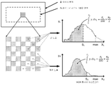
DR의 이러한 확장은 전형적으로 넓은 혹은 고 동적범위(WDR, WiDy 또는 HDR)이라 칭할 수 있다. 이 시스템에서, 장면의 조명은 이미지 센서에 의한 프레임 캡처에 동기될 수 있는, 단색의 고속 광 펄스에 의해 제공될 수 있다. 각 프레임은 단일 파장의 광 혹은 파장들의 임의의 조합, 예를 들면 3개를 수신할 수 있다. 컬러 변조는 프레임별로 행해질 수 있기 때문에, 센서는 단색일 수 있고, 이는 공간적 해상도에 대해 현저한 잇점을 갖는다. 본원에 기술된 이중 노출의 특정한 방법은 두 노출에 대해 개능한 가장 과립적 이상적인 공간 세그먼트화 배열로서 체크보드 패턴을 제공함에 있어 어레이가 단색일 수 있다는 사실을 활용한다.This extension of DR is typically referred to as wide or high dynamic range (WDR, WiDy or HDR). In this system, illumination of the scene can be provided by a monochromatic high speed light pulse, which can be synchronized to frame capture by the image sensor. Each frame can receive a single wavelength of light or any combination of wavelengths, for example three. Since color modulation can be done frame by frame, the sensor can be monochromatic, which has a significant advantage over spatial resolution. The specific method of double exposure described herein takes advantage of the fact that the array can be monochromatic in providing a checkerboard pattern as the most granular ideal spatial segmentation arrangement that is versatile for both exposures.
종국에 어떤 프레임 레이트의 풀 컬러 프레임의 최종의 비디오 시퀀스가 발생될 수 있다. 이것은 상이한 성분들이 상이한 캡처들로부터 도출되고 있기 때문에, 불가피하게 캡처 레이트보다 낮은 레이트일 것이다.Eventually a final video sequence of a full color frame at a certain frame rate can be generated. This will inevitably be a lower rate than the capture rate, since different components are derived from different captures.
몇몇 가능한 체크보드 실시예는 3개의 가용한 단색의 적색, 녹색 및 청색 소스들 중 하나로 각 프레임을 스트로브하는 것을 수반한다. 녹색 정보는 사람 눈에 의해 인지되는 루미넌스는 스펙트럼의 녹색 지역에서 피크가 되기 때문에, 상세에 관하여 청색 및 적색보다 더 가치가 있을 수 있다. 이러한 이유로, 컬러 필터의 널리 사용되는 바이에르 패턴은 적색이나 청색보다 녹색 광의 검출에 대해 2배의 많은 화소를 제공한다. 단색의 프레임 시퀀싱에 있어서, 4개 중 2개는 녹색인 4개 프레임의 반복하는 시퀀스, 즉, G-R-G-B를 채용하는 것이 잇점이 있을 수 있다. 또한, 녹색 데이터는 사람 망막에서 로드(rod)는 저 광 레벨에서 더 감응할 수 있기 때문에, 동적범위에 관하여 더 중요할 수 있다. 그러므로, 이중 노출은 녹색 프레임에 대해서만 적용될 수도 있을 것이다. 가장 기본적인 실시예는 화소들 중 절반을 녹색 프레임에 대해 짧은 노출이 되게 구성하고 다른 절반은 모든 녹색 프레임에 대해 동일한 방식으로 긴 노출로서 구성될 수 있다.Some possible checkboard embodiments involve strobing each frame with one of three available solid red, green and blue sources. Green information can be more valuable than blue and red for details, as the luminance perceived by the human eye peaks in the green region of the spectrum. For this reason, the widely used Bayer pattern of color filters provides twice as many pixels for the detection of green light than red or blue. In monochromatic frame sequencing, it may be advantageous to employ a repeating sequence of four frames, two of which are green, that is, G-R-G-B. In addition, green data may be more important with respect to dynamic range, since rods in the human retina are more sensitive at low light levels. Therefore, double exposure may be applied only to the green frame. The most basic embodiment can configure half of the pixels to have short exposures to the green frame and the other half can be configured as long exposures in the same way for all green frames.
이제 도 1을 참조하면, 특정 부-세트의 화소(101)가 긴 노출로서 구성되는 것과 연속적인 녹색 프레임들 상에 짧은 노출로서 구성되는 것을 교번시키는 잇점이 있는 실시예가 도시되었다. 이 특정 실시예가 도 1에 도시되었고, 여기에서 L 및 S 첨자는 녹색(G), 적색(R), 및 청색(B) 프레임들에 관하여 각각 긴 노출 및 짧은 노출을 나타내고, 다른 도면들에서는 컬러 수법이 다른 표기된다. 도 1 및 도 2에 도시된 바와 같이, 짧은 노출 화소는 103으로 나타내었고 긴 노출 화소는 105로 나타내었다. 이러한 접근법은 보간된 위치가, 연속적으로 프레임마다, 주어진 노출에 대해 실제 화소 샘플로 자리를 바꾸기 때문에 인지된 해상도에 대해 잇점을 제공할 수 있다.Referring now to FIG. 1, an embodiment with the advantage of alternating that a particular sub-set of
펄싱된 단색의 광원들을 이용하는 다른 방법들이 가능할 수 있음을 알 것이다. CONTINUOUS VIDEO IN A LIGHT DEFICIENT ENVIRONMENT 명칭의 함께 계류중인 미국특허 출원번호 13/952,518을 본원에 전체가 개시된 것이 되게 이 발명에 참조로서 포함시킨다. 한 특정한 잇점은 적합한 펄스 에너지 부분을 갖고 동시에 적색, 녹색 및 청색 소스들을 펄싱함으로써 순 루미넌스 (Y) 정보를 제공하는 것일 수 있다. 크로미넌스-적색(Cr) 및 크로미넌스-청색(Cb) 정보는 모든 펄스 에너지가 포지티브하게 하기 위해서 각 경우에 충분한 루미넌스를 추가함으로써 프레임을 번갈아 제공될 수 있다. 이미지 처리 체인은 적용된 부분을 안다면 실제 컬러 공간에서 데이터를 추출할 수 있다. 이러한 상황에서, 이중 노출은 도 2에 나타낸 바와 같이 가장 필요로 될 수 있을 루미넌스 프레임들 상에 적용될 수 있다.It will be appreciated that other methods using pulsed monochromatic light sources may be possible. CONTINUOUS VIDEO IN A LIGHT DEFICIENT ENVIRONMENT Pending US Patent Application No. 13/952,518, incorporated herein by reference, is hereby incorporated by reference in its entirety. One particular advantage may be to provide net luminance (Y) information by having the appropriate pulse energy portion and simultaneously pulsing red, green and blue sources. The chrominance-red (Cr) and chrominance-blue (Cb) information can be provided alternately by adding sufficient luminance in each case to make all pulse energies positive. The image processing chain can extract data from the real color space if you know where it is applied. In this situation, double exposure can be applied on the luminance frames that may be most needed, as shown in FIG. 2.
이중 노출 샘플링의 적용은 녹색 또는 루미넌스 프레임들로 제한되지 않을 수 있고 장면 내 상황이 이를 보장한다면, 또 다른 실시예는 도 3에 도시된 바와 같이 독립적인 이중 노출 비가 적색 프레임 및 청색 프레임에 적용되게 할 수도 있다. 도 4는 루미넌스-크로미넌스 광 펄싱에 대한 동등한 경우를 도시한 것이다.The application of double exposure sampling may not be limited to green or luminance frames, and if the situation in the scene ensures this, another embodiment is such that an independent double exposure ratio is applied to the red and blue frames as shown in FIG. 3. You may. 4 shows an equivalent case for the luminance-chrominance optical pulsing.
도 5는 저-노이즈, 상관된 이중 샘플링을 용이하게 하는데 필요한 4개의 트랜지스터를 가진 통상의 비공유된 화소(500)를 위한 회로도이다. 도시된 바와 같이, 화소(500)를 동작시키기 위해 요구되는 5개의 서비스 와이어가 있을 수 있다. 2 이상의 이웃한 화소(500) 간에 4개의 트랜지스터 중 3개를 공유하는 것이 가능할 수 있고, 이것은 광다이오드를 위한 가용한 영역을 증가시킨다. 화소 크기가 감소됨에 따라 광다이오드는 영역의 더 작은 부분을 점유하기 때문에 양자 효율을 유지하기가 더 어렵게 된다. 공유는 특히 작은 화소 장치를 위해, 센서 제조자가 일반적으로 사용할 수 있는 접근법일 수 있다. 트랜지스터 공유에 의해 제공되는 또 다른 이익은 화소당 요구되는 평균 와이어 수에 감소일 수 있다.5 is a circuit diagram for a conventional
도 6은 통상의 2-웨이 수직 공유를 가진 어레이를 위한 유닛 셀을 도시한 것이다. 3개의 트랜지스터가 공유될 수 있기 때문에, 두 화소당 총 5개의 트랜지스터, 즉 화소당 2.5 트랜지스터가 있을 수 있다. 와이어 라우팅에 관하여, 총 6개의 와이어가 화소쌍마다 필요할 수 있다. 이들 중 4개는 수평으로 라우팅될 수 있고 이들 중 2개는 수직으로 라우팅될 수 있어 각 차원에서 화소 에지 당 2개가 된다. 이것은 화소 에지당 3개의 수평 및 2개의 수직 와이어를 갖는 비공유 경우와는 대조적일 수 있다.6 shows a unit cell for an array with conventional 2-way vertical sharing. Since three transistors can be shared, there can be a total of five transistors per two pixels, 2.5 transistors per pixel. With respect to wire routing, a total of 6 wires may be required per pixel pair. Four of these can be routed horizontally and two of them can be routed vertically, two per pixel edge in each dimension. This may be in contrast to the non-shared case with 3 horizontal and 2 vertical wires per pixel edge.
접근법은 수직 대신에 수평으로 화소를 쌍을 이루는 것일 수 있다. 이것은 4개의 수평 와이어가 이제 단일 화소 에지에 들어맞을 수 있기 때문에, 와이어 라우팅 단순성에 관하여 통상적으로 덜 유리할 수 있다. 도 7을 참조한다. 그러나, 이 라우팅 단점을 능가하는 2개의 현저한 이익이 있을 수 있다.The approach may be to pair pixels horizontally instead of vertically. This can typically be less advantageous with respect to wire routing simplicity, since the four horizontal wires can now fit on a single pixel edge. See FIG. 7. However, there can be two significant advantages over this routing disadvantage.
제 1 이익은 순 회로의 절반만이 각 컬럼에 서비스하기 위해 요구될 수 있다는 것이다. 이것은 컬럼 회로가 칩 공간의 주 소비자일 수 있기 때문에 전체 칩 영역을 감소시키는데 도움을 준다. 도 8에 도시된 바와 같이, 단일 컬럼 회로는 2 대신 화소들의 4개의 컬럼에 서비스할 수 있고, 이는 수직 2-웨이 공유에 대한 경우가 될 것이다.The first benefit is that only half of the net circuit can be required to service each column. This helps to reduce the overall chip area since the column circuit can be the main consumer of the chip space. As shown in Figure 8, a single column circuit can serve four columns of pixels instead of two, which will be the case for vertical two-way sharing.
제 2 이익은 수평 공유가 행당 2개의 독립적인 TX 신호를 제공하는 것일 수 있다. 이것은 도 8에 도시된 바와 같이 홀수 컬럼과 짝수 컬럼 간에 교번하는, 단일 행 내 2개의 독립적인 노출을 가질 가능성을 연다. 이중 노출의 체크보드 배열은 교번하는 행들 상에 TX1 및 TX2 홀수/짝수 컬럼 연관들을 스위칭하는 것에 의해 이제 가능해질 수 있다. 도 8은 이것이 일 실시예에 있어 매 제 2 행에 대해 TX1/TX2 라우팅에 "트위스트"를 삽입함으로써 어떻게 행해질 수 있는가를 나타낸다. 이 유형의 홀수-짝수 노출 패턴은 단색 센서들의 경우에만 적용될 수 있다. 컬러 센서는 서로 다른 컬러 필터들을 가진 이웃 화소들을 가지며 그러므로 홀수/짝수 노출 변조는 백색 밸런스를 변경하는 데에만 효과적일 것이고 동적범위를 증가시키지는 않을 것이다.The second benefit may be that horizontal sharing provides two independent TX signals per row. This opens the possibility of having two independent exposures in a single row, alternating between odd and even columns as shown in FIG. 8. The double exposure checkboard arrangement can now be enabled by switching the TX1 and TX2 odd/even column associations on alternating rows. Figure 8 shows how this can be done by inserting a "twist" in TX1/TX2 routing for every second row in one embodiment. This type of odd-even exposure pattern can only be applied to monochromatic sensors. The color sensor has neighboring pixels with different color filters and therefore odd/even exposure modulation will only be effective in changing the white balance and will not increase the dynamic range.
다른 실시예에서, 행에서 행으로 TX1/TX2 할당의 스위칭은 어레이 일측에 행 드라이버 회로의 2개의 교번하는 플래버(flavor)에 의해서, 혹은 홀수 및 짝수 행 내에서 상이하게 TX1/TX2 라우팅을 형성함으로써 달성될 수 있다.In another embodiment, the switching of the TX1/TX2 assignment from row to row forms TX1/TX2 routing differently by two alternating flavors of row driver circuits on one side of the array, or within odd and even rows. Can be achieved.
이제 도 9를 참조하면, 풀-프레임 통합을 가진 롤링 셔터 CMOS 센서에 대한 일반적인 타이밍 상황이 도시되었다. 도면에서, 대각선은 화소의 행을 롤링할 때 판독 및 리셋 포인터의 동작을 나타낸다. 이 기간은 광학 흑색 또는 광학적 블라인드(OB) 행(902)(전방 행 및 후방 행 둘 다)이 판독(예를 들면, 판독 프레임(906) 동안)될 수 있는 시간, 블랭킹 시간(908), 및 이전 화소 데이터가 아닐 수 있는 임의의 다른 데이터가 발행(예를 들면, 서비스 라인 시간)될 수 있는 시간을 포함한다.Referring now to FIG. 9, a typical timing situation for a rolling shutter CMOS sensor with full-frame integration is shown. In the figure, diagonal lines indicate the operation of the read and reset pointers when rolling rows of pixels. This period is the time during which the optical black or optical blind (OB) row 902 (both the front row and the rear row) can be read (eg, during the read frame 906), the
프레임별로 광 컬러를 변조하는 원리는 센서가 단색일 수 있고 이에 따라 예를 들면 바이에르 기반의 등가물보다 높은 해상도를 가질 수 있게 하는 것일 수 있다. 페널티는 단일 풀 컬러 이미지를 생성하기 위해 다수의 프레임이 판독될 수 있다는 것일 수 있다. 그러나, 이 페널티는 센서가 대응하여 빠르게 판독될 수 있다면 없어지게 되고 프레임 레이트가 회복될 수 있다.The principle of modulating the optical color on a frame-by-frame basis may be that the sensor may be monochromatic and thus have a higher resolution than, for example, a Bayer-based equivalent. The penalty may be that multiple frames can be read to produce a single full color image. However, this penalty can be eliminated if the sensor can be read quickly correspondingly and the frame rate can be recovered.
도 10 및 도 11은 어레이 내 다수 세트의 화소가 서로 다른 정도의 광을 통합하는 두 대안적 방법들에 대한 타이밍을 도시한 것이다. 노출 변조는 두 전역 TX 펄스들로서 전역 TX1 및 전역 TX2에 의해 달성될 수 있다. 이들은 광 펄스 에지(들)과 조합되었을 때 2개의 전역 셔터를 효과적으로 생성한다.10 and 11 show timing for two alternative methods in which multiple sets of pixels in an array incorporate different degrees of light. Exposure modulation can be achieved by global TX1 and global TX2 as two global TX pulses. These effectively create two global shutters when combined with light pulse edge(s).
통합 기간의 끝에서, 롤링 포인터는 판독을 위한 신호를 전송하기 위해서 또 다른 TX 펄스를 제공한다. 설명 목적을 위해서, 체크보드 패턴으로(위에 기술된 바와 같이) 서로 다른 노출들의 두 세트의 화소의 경우가 주로 강조될 것이다. 그러나, 이 발명의 범위는 더 많은 수의 화소 유형(즉, 노출) 및 대안적 물리적 화소 유형 배열들을 가진 경우들을 포함하게 의도된 것에 유의한다. 공간 패턴은 화소 세트의 수, 화소 레이아웃, 화소 어레이 배열 및 주변 회로에의화소 어레이 연결에 의존한다.At the end of the integration period, the rolling pointer provides another TX pulse to transmit a signal for reading. For illustrative purposes, the case of two sets of pixels of different exposures in a checkerboard pattern (as described above) will be mainly emphasized. Note, however, that the scope of this invention is intended to cover cases with a larger number of pixel types (i.e., exposure) and alternative physical pixel type arrangements. The spatial pattern depends on the number of pixel sets, pixel layout, pixel array arrangement, and pixel array connections to peripheral circuits.
혼란을 피하기 위해서 롤링 TX 신호를 본원에서는 TX1 및 TX2라 지칭하고, 전역 TX 신호를 전역 TX1 및 전역 TX2라 한다. 전역 펄스는 어레이 내 모든 부착된 화소에 동시에 영향을 미친다. 비-전역 펄스는 롤링 포인터를 통해 인가될 수 있다.To avoid confusion, rolling TX signals are referred to herein as TX1 and TX2, and global TX signals are referred to as global TX1 and global TX2. Global pulses simultaneously affect all attached pixels in the array. Non-global pulses can be applied through the rolling pointer.
CMOS 이미지 센서로부터 알 수 있는 것들은 전역 셔터의 이 방법이 연속 조명과 함께 사용될 때 전역 셔터에 연관된 문제가 나타나지 않음에 유의한다. 이 경우에, 신호는 상당한 기간 동안 누설 플로팅 확산 노드 상에 저장될 수 있고, 펄싱된 조명과 함께 여기에 기술된 두 방법에 있어서, 이익은 광신호를 저장하기 위해 광다이오드로부터 취해질 수 있다.Note that what can be seen from the CMOS image sensor does not present a problem associated with the global shutter when this method of global shutter is used with continuous lighting. In this case, the signal can be stored on a leaky floating diffusion node for a considerable period of time, and for the two methods described herein with pulsed illumination, benefits can be taken from the photodiode to store the optical signal.
화소는 이들의 전송 (TX) 및 리셋 (RST) 트랜지스터들이 온(즉, 도면에서 하이(high) 상태)으로 유지되는 한, 리셋에 유지될 수 있음에 유의한다. 이 상태에서 광다이오드 내 임의의 전류는 서플라이에 보내질 수 있다.Note that the pixels can be held at reset as long as their transmit (TX) and reset (RST) transistors are kept on (ie, high in the figure). In this state, any current in the photodiode can be sent to the supply.
통합 기간은 TX 트랜지스터가 턴 오프되었을 대 시작한다(도면에서 로우(low)). 이제 도 10을 참조하면, 모든 화소는 리셋 모드에 유지될 수 있고, 그러므로 전역 TX1, 전역 TX2 및 전역 RST가 모두 하이일 수 있을 때, 플러시될 수 있다. 전역 TX2가 로우가 되었을 때, TX2에 부착된 어레이 내 모든 화소는 통합하기 시작한다. P2 광 펄스가 발생하였을 때, 이의 대응하는 광-전하는 TX2 화소들에 의해 통합될 수 있다. 그러나, 전역 RST 신호 및 전역 TX1 신호는 여전히 하이일 수 있기 때문에, TX1 화소에서 P2 펄스에 의해 생성된 임의의 광전하는 흘러나갈 수 있다. 전역 TX1이 로우가 되었을 때, TX1 화소들은 통합하기 시작한다. 이 시점에서, TX2 화소는 P2 펄스를 완전히 통합하였을 것이며 TX1 화소는 아무 것도 통합하지 않았을 것이다. P1 광 펄스가 발생하였을 때, TX1 및 TX2 화소 둘 다에 의해 통합될 수 있다. 그러므로 시퀀스의 끝에서, TX1 화소는 단지 P1 광 펄스로부터 비롯되는 순 광전하를 가질 것이며 TX2 화소는 광 펄스 둘 다를 통합하였을 것이다.The integration period starts when the TX transistor is turned off (low in the figure). Referring now to FIG. 10, all pixels can be maintained in a reset mode, and therefore can be flushed when global TX1, global TX2 and global RST can all be high. When global TX2 goes low, all pixels in the array attached to TX2 begin to merge. When a P2 light pulse occurs, its corresponding light-charge can be incorporated by the TX2 pixels. However, since the global RST signal and the global TX1 signal can still be high, any photocharge generated by the P2 pulse in the TX1 pixel can flow out. When global TX1 goes low, the TX1 pixels begin to merge. At this point, the TX2 pixel would have fully integrated the P2 pulse and the TX1 pixel would have not integrated anything. When a P1 light pulse occurs, it can be integrated by both TX1 and TX2 pixels. So at the end of the sequence, the TX1 pixel will only have a net photocharge coming from the P1 light pulse and the TX2 pixel will incorporate both light pulses.
도 11은 대안적 이중 조명 실시예에 대한 유사한 타이밍도일 수 있다. 2개의 개별적인 개개의 광 펄스를 착수하는 대신에, 단일의 광 펄스는 두 TX 트랜지스터가 턴 오프될 수 있는 기간 동안 계속 남아 있는다. 통합된 광은 TX 하강에지와 광 펄스 하강에지 사이의 시간에 비례할 수 있고, 그러므로 상이한 화소 응답들은 전역 TX1 하강에지와 전역 TX2 하강에지를 스태거함으로써 달성될 수 있다. 도시된 예에 있어서, TX1 화소는 광 펄스에 의해 발생된 광의 -1/3을 통합하고 TX2는 총 펄스 에너지의 -2/3을 통합한다.11 may be a similar timing diagram for an alternative dual lighting embodiment. Instead of undertaking two separate individual light pulses, a single light pulse remains for a period during which both TX transistors can be turned off. The integrated light can be proportional to the time between the TX falling edge and the light pulse falling edge, so different pixel responses can be achieved by staggering the global TX1 falling edge and the global TX2 falling edge. In the illustrated example, the TX1 pixel incorporates -1/3 of the light generated by the light pulse and TX2 incorporates -2/3 of the total pulse energy.
또 다른 실시예에서, 이중 조명은 도 10 타이밍과 도 11 타이밍의 혼합으로 달성될 수 있다. 전역 TX2 신호는 단일 광 펄스의 상승에지 전에 자신의 로우 상태로 복귀할 것이며, 이것은 TX2 화소가 광 펄스의 전체 에너지를 통합하게 할 것이다.In another embodiment, dual illumination can be achieved with a mixture of timings of FIG. 10 and FIG. The global TX2 signal will return to its low state before the rising edge of a single light pulse, which will cause the TX2 pixel to incorporate the total energy of the light pulse.
이 경우에 이중 노출은 도 10 및 도 11에 관하여 기술된 서로 다른 타이밍들에 의해 달성될 수 있고, 더 많은 수의 조명은 동일 블랭킹 시간 동안 광 펄스의 수를 증가시킴으로써 달성될 수 있다.Double exposure in this case can be achieved by the different timings described with respect to FIGS. 10 and 11, and a greater number of illuminations can be achieved by increasing the number of light pulses during the same blanking time.
도 12는 제어된, 펄싱된 조명이 있는 데서 내시경 이미징의 목적으로, 최소 영역 커스텀 센서의 실시예의 내부 타이밍을 도시한 것이다. 각 프레임 기간은 단색 광 펄싱 및 다수의 화소 조명을 위해 최적화될 수 있는 4개의 구별되는 국면들을 포함할 수 있다. 국면 1 및 3 동안에, 데이터가 센서로부터 발행될 수 있는데, 이것은 물리적 화소로부터 신호 샘플이 아닐 수 있다. 그보다는 이들은 카메라 시스템에 칩의 동기화 및 데이터 록(lock)에 관계된 데이터일 수 있다. 이들 "서비스 라인" 기간은 내부 및 외부 모니터링을 위해서 그리고 라인 내 어떤 유형의 비-화소 데이터의 엔코딩을 위해서 사용될 수 있다. 이러한 내부 모니터링은 센서 온도, 및 이에 더하여 어떤 전압 및 전류를 포함할 수 있다. 외부 모니터링은 핸드-피스 버튼 활동 혹은, 예를 들면, 내시경의 각도의 측정으로부터의 데이터를 포함할 수 있다. 국면 2는 센서 롤링 판독(내부 타이밍 및 동기화)에 관계될 수 있고 국면 4는 센서 구성의 목적을 위한 것일 수 있다. 구성 국면 동안에, 센서 출력 데이터 라인들은 인입 구성 코맨드를 받아들이기 위해 반대가 될 수 있다. 그러므로 카메라 제어기는 국면 4 기간에 동기될 수 있다. 또한, 국면 4는 도 10 및 도 11에 도시된 동작이 수행될 수 있는 전역 셔터 국면에 두배이다. 이 이유로, 국면 4는 광 펄싱 시스템과도 동기될 수 있다.12 shows the internal timing of an embodiment of a minimal area custom sensor for the purpose of endoscopic imaging in the presence of controlled, pulsed illumination. Each frame period can include four distinct phases that can be optimized for monochromatic light pulsing and multiple pixel illumination. During
전역 신호(전역 TX1, 전역 TX2 및 전역 ST)의 펄스 폭 및 타이밍은 완전히 프로그램가능할 수 있고 국면 4는 가변 길이를 가진 유일한 국면일 수 있음에 유의한다. 이것은 현재의 프레임의 유형이 주어졌을 때, 가용 광 파워에 맞추기 위해서 가용 펄스 시간이 조율될 수 있게 한다. 개개의 파장 소스들은 예를 들면, 최대 가용 광 파워, 양자 효율 및 응답 시간에 관하여 현저히 서로 다를 수 있다. 중요할 수 있는 것은 최종 프레임 레이트가 적합한 다수의 평균 캡처 레이트일 수 있다는 것일 수 있다. 그밖에, 프레임 유형의 반복되는 패턴 내에서 임의의 변동은 이미지 신호 처리 체인(ISP) 내에서 적합한 버퍼링에 의해 해결될 수 있다. 도 13은 4개의 서로 다른 프레임 길이 및 4개의 최대-허용된 광 변조를 받아들이는 4개의 서로 다른 블랭킹 시간들을 가진 4-프레임 사이클의 예를 도시한 것이다.Note that the pulse width and timing of the global signals (global TX1, global TX2 and global ST) can be fully programmable and phase 4 can be the only phase with variable length. This allows the available pulse time to be tuned to match the available optical power given the current frame type. The individual wavelength sources can differ significantly, for example, with respect to maximum available optical power, quantum efficiency and response time. What may be important may be that the final frame rate can be any number of suitable average capture rates. In addition, any fluctuations within a repeating pattern of frame type can be resolved by appropriate buffering within the image signal processing chain (ISP). 13 shows an example of a four-frame cycle with four different frame lengths and four different blanking times to accept four maximum-allowed light modulations.
도 14는 Y-Cb-Y-Cr 패턴에 기여될 수 있는, 도 2에 도시된 프레임 시퀀스에 대한 타이밍도이다. 모든 3개의 소스는 루미넌스 프레임, 즉 프레임 #1 및 #3 동안 파이어될 수 있다. 프레임 #2 및 #4는 루미넌스의 임계적으로 조율된 혼합에 의해, 단일 파장 펄스를 가진 Cb 및 Cr 정보를 각각 제공할 수 있다.14 is a timing diagram for the frame sequence shown in FIG. 2, which may contribute to the Y-Cb-Y-Cr pattern. All three sources can be fired during the luminance frame, ie frames #1 and #3.
동적범위 향상에 대한 또 다른 접근법은 신호의 공간 비닝(spatial binning)에 의해 제공될 수 있다. 단색 센서를 취하는 추가의 잇점은 이웃 화소들이 함께 비닝될 수 있다는 것일 수 있다. 비닝은 공간적 해상도를 희생하고, 신호에 더 크게 도달할 수 있게 하고 이에 따라 DR을 더 커지게 한다.Another approach to dynamic range enhancement can be provided by spatial binning of the signal. An additional advantage of taking a monochromatic sensor may be that neighboring pixels can be binned together. Binning sacrifices spatial resolution, allowing the signal to reach larger and thus making the DR larger.
정밀하게 비닝이 어디에서 일어나는가는 DR을 확장함에 있어 비닝의 유효성을 좌우한다. 예를 들어 2개의 이웃한 화소의 비닝을 취한다, (2-웨이 비닝). 비닝이 디지털 영역에서 행해질 수 있다면, 신호의 추가의 팩터 2(6dB)이 실현될 수 있다. 그러나, 2개의 아날로그 샘플이 있을 수 있고, 각각은 노이즈 향상의 팩터 √2 (3dB)에 이르는 동일 량의 판독 노이즈에 기여한다. 그러므로, 판독-노이즈 소스보다 체인 내 나중에 시점에서 2개의 화소로부터 데이터의 비닝은 추가의 DR의 3dB에 이른다. 그러나, 비닝이 충전 영역에서, 즉, 앞서 기술된 바와 같이 화소 레벨에서 수행될 수 있다면, 실현될 수 있는 추가의 DR은 판독 노이즈의 추가가 신호의 합산 후에 일어나기 때문에, 6dB일 수 있다.Exactly where binning takes place determines the effectiveness of binning in extending DR. For example, binning of two neighboring pixels is taken (2-way binning). If binning can be done in the digital domain, an additional factor 2 (6 dB) of the signal can be realized. However, there can be two analog samples, each contributing to the same amount of read noise, up to a noise enhancement factor of √2 (3dB). Therefore, binning of data from two pixels at a later point in the chain than the read-noise source leads to 3 dB of additional DR. However, if binning can be performed in the charging area, ie at the pixel level as described above, the additional DR that can be realized can be 6 dB, since the addition of readout noise occurs after the summation of the signals.
앞서 기술된 2-웨이 공유된 아키텍처는 충전 영역에서 2-웨이 비닝의 이러한 수단만을 제공한다. TX1 및 TX2 신호들의 동시적인 펄싱은 광-신호 둘 다가 공유된 플로팅 확산에 동시에 전송되게 한다. 후속하여 각 행이 판독될 수 있을 때, 비닝되지 않은 경우와 비교했을 때, 동인 노이즈를 갖고 충전 범위에 두 배를 가지며, 그러므로 가외의 DR의 6dB를 갖는다.The two-way shared architecture described above provides only this means of two-way binning in the charging area. Simultaneous pulsing of the TX1 and TX2 signals allows both optical-signals to be transmitted simultaneously in a shared floating spread. Subsequently, when each row can be read, it has driver noise and doubles the filling range when compared to the non-binning case, and thus has 6dB of extra DR.
실시예는 이중 노출 제어를 포함할 수 있다. 이 유형의 동적범위(DR) 향상(즉, 이중 노출)의 최적의 효과적인 동작에 키는 노출 시간 비에 대한 연속적인 제어일 수 있다.Embodiments may include double exposure control. This type of dynamic range (DR) enhancement (i.e., double exposure) can be a continuous control over the exposure time ratio that is key to optimal effective operation.
특히, 먼저 장면이 요구하지 않는다면, 즉 장면의 동적범위가 화소의 본연의 동적범위 미만일 수 있다면, 동적범위 확장은 전혀 없을 것이다. 두 번째로, 장면의 동적범위가 화소보다 클 수 있다면, 추가된 동적범위의 량은 이에 최소 마진을 제공하기에 충분할 것이다.In particular, if the scene is not required first, that is, if the dynamic range of the scene can be below the natural dynamic range of the pixel, there will be no dynamic range expansion at all. Second, if the dynamic range of the scene can be larger than the pixels, the amount of added dynamic range will be sufficient to provide a minimum margin for it.
이에 대한 이유는 인위적 동적범위 확장이 항시 비용이 든다는 것일 수 있다. 이 발명에서 기술되는 방법에 있어서는 증가하는 노출 비에 따라 차등적으로 증가하는 공간적 해상도 비용이 존재할 수 있다. 최대 노출 비의 제한에서, 큰 혹은 낮은 광휘 장면 지역들에 대해서, 유용한 이미지 콘텐트의 대다수는 노출들 중 단지 하나만으로부터 온다. 이 극단에서, 해상도는 x 및 y로 화소 수의 1/2 배를 갖는 것에 상응하는 것에 점근적으로 접근하고 이어 보간에 의해 업-스케일링한다. 다른 극단에서, 비가 1(unity)일 수 있을 때, DR 확장은 없고 페널티는 없을 수 있다.The reason for this may be that an artificial dynamic range expansion is always expensive. In the method described in this invention, there may be differentially increasing spatial resolution costs with increasing exposure ratios. At the limit of the maximum exposure ratio, for large or low luminance scene areas, the majority of useful image content comes from only one of the exposures. At this extreme, the resolution is asymptotically approached to corresponding to having 1/2 times the number of pixels in x and y and then up-scaled by interpolation. At the other extreme, when the ratio can be 1, there is no DR extension and no penalty.
일반적으로, 무작위로 변하는 조명 시나리오를 경험하는, 캠코더와 같은 디지털 카메라는 가용한 DR를 최상으로 항시 이용하기 위해서 센서 동작 조건을 연속적으로 조절하는 수단을 탑재한다. 이 프로세스는 자동-노출로서 알려져 있다. 전형적으로, 예를 들어, 통합 시간(셔터), 아날로그 이득, 디지털 이득, 애퍼처, 등을 포함하여, 기정의된 테이블에 따라 조절될 수 있는 몇가지 변수들이 있을 수 있다. 도 15는 셔터 시간, 아날로그 이득 및 디지털 이득을 탑재하는 시스템을 위한 가상적 테이블의 예이다. 점등 자체는 통상적으로, 스틸 캡처를 위해 사용되는 플래시 조명은 제외하고 카메라의 제어를 벗어날 수 있다.In general, digital cameras, such as camcorders, which experience randomly changing lighting scenarios, are equipped with means to continuously adjust the sensor operating conditions in order to make the best use of the available DR. This process is known as auto-exposure. Typically, there may be several variables that can be adjusted according to a predefined table, including, for example, integration time (shutter), analog gain, digital gain, aperture, and the like. 15 is an example of a virtual table for a system with shutter time, analog gain and digital gain. The lighting itself is usually outside the control of the camera, except for the flash lighting used for still capture.
이 발명은 구체적으로, 연속된 비디오 캡처를 위해, 프레임별로, 펄싱된 적색, 녹색 및 청색 조명의 량에 대한 완전히 제어할 수 있는 카메라 시스템에 관한 것일 수 있다.The invention may specifically relate to a fully controllable camera system for the amount of pulsed red, green and blue illumination, frame by frame, for continuous video capture.
이러한 펄싱된 조명 시스템의 경우에, 장면 조도는 카메라 또는 이미징 장치의 제어 하에 있을 수 있다. 그러므로 전체 광 펄스 에너지는 실질적으로 셔터를 대신한다. 더 많은 광신호는 더 높은 SNR을 갖게 하기 때문에, 광 에너지는 화소의 선택된 중앙 지역의 분포의 선택된 백분위수에 대해서, 요망되는 디지털 신호 레벨이 ISP 체인 내에서 도달될 수 있을 때까지 증가될 수 있다. 아날로그 이득은 화소 신호 용량(최대의)의 분포의 최하위가 (센서에 있어 어떤 센서 변동이 일어나) ADC의 상측 레일 바로 위일 수 있는 이득인 것으로 간주될 수 있는 최소 설정에 유지될 수 있다. 최대 광 펄스 에너지는 프레임의 가용한 부분의 구간에 의해서 그리고 예컨대 레이저 다이오드 또는 LED 전류에 의해 제공되는 최대 전자기 에너지에 의해 제한될 수 있다. 이 제한에 도달될 수 있을 때만 임의의 이득이 적용될 수 있다. R-G-B-G 펄스 시퀀스 경우에 있어서, 최상의 전체 SNR은 3개의 프레임 유형들을 독립적으로 모니터하고 제어하고(모든 광자 플러스를 최대화하기 위해) 컬러들 중 2개를 백색 밸런스 목적을 위해 ISP에서 디지털 방식으로 감쇄시킴으로써 얻어질 수 있다. 백색 밸런스에 대한 대안적 접근법은 상대적 R, G 및 B 펄스 에너지들을 변조하는 것일 수 있다. 이 접근법은 낮은 최송의 신호 대 노이즈 비(SNR)을 갖는데, 그러나 여전히 노이즈의 인지를 향상시킬 1(unity)보다 클 수 있는 임의의 디지털 백색 밸런스 이득에 대한 필요성을 제거한다.In the case of such a pulsed lighting system, the scene illumination may be under the control of a camera or imaging device. Therefore, the total light pulse energy substantially replaces the shutter. Since more optical signals have a higher SNR, the optical energy can be increased for a selected percentile of the distribution of a selected central region of pixels until the desired digital signal level can be reached within the ISP chain. . The analog gain can be maintained at a minimum setting where the lowest of the distribution of pixel signal capacities (maximum) can be considered to be the gain that can be just above the upper rail of the ADC (some sensor variation in the sensor). The maximum light pulse energy can be limited by the section of the available portion of the frame and by the maximum electromagnetic energy provided by, for example, a laser diode or LED current. Arbitrary gains can be applied only when this limit can be reached. In the case of the RGBG pulse sequence, the best overall SNR is obtained by independently monitoring and controlling three frame types (to maximize all photons plus) and two of the colors digitally attenuated by the ISP for white balance purposes. Can lose. An alternative approach to white balance may be to modulate relative R, G and B pulse energies. This approach has a low maximum signal-to-noise ratio (SNR), but still eliminates the need for any digital white balance gain that can be greater than 1 (unity) to improve the perception of noise.
노출 시간 비(및 이에 따라 DR 확장의 범위)를 제어하기 위해서, 체크보드 패턴으로 존재하는 화소의 두 플래버에 대해 WDR 통계가 독립적으로 수집될 수 있다. 이것은 선택적으로 적색, 녹색 및 청색 프레임들에 대해 독립적으로 행해질 수 있다. 이미지의 지역에 대한 흑색-정정된 신호의 두 대응하는 히스토그램이 구축될 수 있다. 히스토그램들 중 하나는, 앞서 언급된 바와 같이, 분포의 선택된 백분위수(PL)를 표적 신호 레벨(SL, 예를 들면 디지털 DR의 50%)에 비교함으로써, 펄스 에너지 레벨을 제어하기 위해, 사용될 수 있다. 이 유형-1 화소의 노출 시간 TL은 최대에 유지될 수 있다. 첨자 L은 긴 노출을 나타낸다. 분포의 또 다른 선택된 백분위수 PS를 비교하고, Ps > PL, 이것을 상이한 신호 레벨(SS)와 비교함으로써, SS > SL, 장면의 DR을 모니터하기 위해 다른 히스토그램이 사용될 수 있다. 첨자 S는 짧은 노출을 나타낸다. SS는 일반적으로 디지털 DR의 최상위에 가깝게 조율될 수 있다. PS≤SS이라면, 이들 유형-2 화소에 대한 노출 시간(TS)은 최대에 유지될 수 있다. PS >SS이라면, TS는 PS = SS가 될 때까지 낮을 수 있다. 도 16을 참조한다. 어떤 시점에서 DR 향상에 기인하여 이미지 질 열화가 이익보다 크기 때문에, 노출 시간 비 증가가 얼마나 많게 허용될 수 있는가에 관하여 기정의된 제한(E)이 있을 수 있다. PL, PS, SL, SS 및 E 값들은 상이한 응용들에 따라 서로 다르게 조율되고 공장 선조정으로서 저장될 수 있다. 노출 시간(TL, TS)는 WDR 융합 프로세스(이하 더욱 논의된다)에 의해 그리고 컬러 융합 ISP 스테이지에 의한 사용을 위해, 각 프레임 유형에 대해 기록될 수 있다. 백색 밸런스의 목적을 위해 적색, 녹색 및 청색 펄스 에너지들이 변조될 수 있는 경우에, 적색 및 청색 프레임들에 대한 노출 시간은 WDR 통계를 모으기 위해서 전용으로 사용될 수 있는 녹색 프레임에 의해 좌우될 수 있다.In order to control the exposure time ratio (and thus the extent of DR expansion), WDR statistics can be collected independently for the two flavors of pixels present in a checkerboard pattern. This can optionally be done independently for red, green and blue frames. Two corresponding histograms of the black-corrected signal for the region of the image can be built. One of the histograms is to control the pulse energy level by comparing the selected percentile (P L ) of the distribution to the target signal level (S L , eg 50% of digital DR), as mentioned above, Can be used. The exposure time T L of this type-1 pixel can be kept at maximum. Subscript L indicates long exposure. By comparing another selected percentile P S of the distribution, P s > P L , and comparing it to a different signal level (S S ), S S > S L , another histogram can be used to monitor the DR of the scene. . Subscript S indicates short exposure. S S can generally be tuned close to the top of the digital DR. If P S ≤S S , the exposure time T S for these type-2 pixels can be kept at a maximum. If P S >S S , T S may be low until P S = S S. See FIG. 16. There may be a predefined limit (E) as to how much an increase in the exposure time ratio can be tolerated, because at some point the image quality degradation due to the DR enhancement is greater than the benefit. P L , P S , S L , S S and E values can be tuned differently according to different applications and stored as factory pre-adjustment. The exposure times (T L , T S ) can be recorded for each frame type, by the WDR fusion process (discussed further below) and for use by the color fusion ISP stage. If the red, green and blue pulse energies can be modulated for the purpose of white balance, the exposure time for the red and blue frames can be dominated by a green frame that can be dedicated to gathering WDR statistics.
Y-Cb-Y-Cr 조명에 있어서, 특정 프레임 유형에 대해 3개의 상대적 펄스 에너지가 일정하게 유지될 수 있다. WDR 제어는 WDR을 독립적으로 크로미넌스 프레임 상에 적용하는 선택을 갖고 베이스라인으로서 루미넌스 프레임에 대해 적용될 수 있다. R-G-B-G 수법에 관해 생 흑색-정정된 프레임 데이터에 대해서 히스토그램이 구축될 수 있다. 다시 WDR 융합 및 컬러 융합을 위해 각 프레임 유형에 대한 노출 시간이 기록될 수 있다.For Y-Cb-Y-Cr illumination, three relative pulse energies can be kept constant for a particular frame type. WDR control has the option of independently applying WDR on the chrominance frame and can be applied to the luminance frame as a baseline. Histograms can be constructed for raw black-corrected frame data for the R-G-B-G technique. Again, exposure time for each frame type can be recorded for WDR fusion and color fusion.
실시예는 ISP에서 진행되는 넓은 동적범위 데이터를 포함할 수 있다. 도 17은 Y-Cb-Y-Cr 펄싱 수법을 사용한 체크보드 WDR를 위한 기본 ISP 배열을 도시한 것이다. WDR 융합은 평균 흑색 오프셋이 제로에 조절되어져 있고 데이터가 사인(signed)될 수 있도록 암 프레임 감산을 따라가는 것이 중요할 수 있다. 또한 FPN이 제거되게 하는 것이 매우 바람직할 수 있다. 융합 프로세스의 목적은 각 프레임에 대해, 두 개별적 노출을 위한 데이터를 컬러 융합에 앞서, 단일 아미지로 조합하는 것일 수 있다. 제 1 단계는 체크보드 패턴의 두 성분을 두 개의 개별적인 버퍼에 분리하고 보간에 의해 갭을 채우는 것(fill in)을 수반한다. 모든 비어 있는 화소는 동일한 로컬 환경을 보기 때문에(이미지의 에지 근방에 화소는 제외하고) 요구되는 단지 한 일반적인 커널이 있을 수 있다. 간단한 선형 보간에 의해 체크보드 패턴을 채우기 위한 적합한 콘볼루션 커널은 다음과 같다:Embodiments may include wide dynamic range data from an ISP. FIG. 17 shows a basic ISP arrangement for a checkerboard WDR using the Y-Cb-Y-Cr pulsing technique. WDR fusion may be important to follow the dark frame subtraction so that the average black offset is adjusted to zero and data can be signed. It may also be very desirable to have FPN removed. The purpose of the fusion process may be to combine data for two separate exposures for each frame into a single image, prior to color fusion. The first step involves separating the two components of the checkerboard pattern into two separate buffers and filling in the gaps by interpolation. Since all empty pixels see the same local environment (except pixels near the edge of the image), there may be only one common kernel required. A suitable convolution kernel for filling a checkerboard pattern by simple linear interpolation is:

보간 후에 각 화소 위치에 대해 2개의 샘플이 있을 수 있다. 도 18은 추가의 DR의 12dB가 되게 할 4의 노출 비에 대해 조도-신호 관계를 도시한 것이다. 이득은 짧은 노출 샘플에 적용될 수 있고, 이것은 노출-시간 비 TL/TS와 같을 수 있다. 이것은 비의 각 팩터 2에 대해 하나의 가외의 비트의 추가를 요구한다. 융합 자체는 두 샘플의 가중된 합을 만드는 것을 수반한다:There may be two samples for each pixel position after interpolation. Figure 18 shows the illuminance-signal relationship for an exposure ratio of 4 that would be 12 dB of additional DR. The gain can be applied to short exposure samples, which can be equal to the exposure-time ratio T L /T S. This requires the addition of one extra bit for each

여기에서 xS 및 xL은 각각 (사인된) 짧은 노출 신호 및 긴 노출 신호일 수 있다. γ 팩터는 긴 노출 신호(xL)의 함수일 수 있고, 두 임계 τ1 및 τ2에 따라 설정될 수 있다. xL=τ1 밑에서 γ=0.0이고 γ=τ2 위에서 γ=0.0이다. 임계 사이에, 다양한 기능 형태가 채용될 수 있다. τ1와 τ2 사이에 γ의 선형 및 입방 행동 예가 도시된 도 19를 참조한다. τ2의 값은 xL의 최대 가능한 값, 예를 들면 이 미만의 어떤 값에 설정될 수 있다. 낮은 임계 τ1의 목적은 이득 팩터 TL/TS가 적용된 짧은 샘플로부터 판독 노이즈의 영향을 제한하기 위한 것일 수 있다. 최대 비 E를 수용하기 위해 줄잡아 높은 상수에 설정될 수 있는데, 그러나 이를 TL/TS에 선형으로 변하게 하는 것이 더 이익이 될 수 있다.Where x S and x L can be (signed) short exposure signals and long exposure signals, respectively. The γ factor may be a function of the long exposure signal x L and may be set according to two thresholds τ 1 and τ 2 . γ=0.0 below x L =τ 1 and γ=0.0 above γ=τ 2 . Between thresholds, various functional forms can be employed. See FIG. 19 showing examples of linear and cubic behavior of γ between τ 1 and τ 2 . The value of τ 2 can be set to the maximum possible value of x L , for example any value less than this. The purpose of the low threshold τ 1 may be to limit the effect of readout noise from short samples with a gain factor T L /T S applied. In order to accommodate the maximum ratio E, it can be rounded up and set to a high constant, but making it linear to T L /T S may be more beneficial.

스티치 프로세스에 따라, 이미지 데이터는 원래의 긴 샘플 및 짧은 샘플이 행하는 것보다 더 많은 수의 비트의 디지털 동적범위를 점유하며, 그러므로 이의 비트 카운트를 다음 스테이지에 앞서 ISP 파이프라인 폭으로 다시 감소되게 하는 것을 필요하다. ISP 파이프라인 폭이 n 비트일 수 있다면, 융합된 이미지는 m 비트를 가지며 (m-n)은 다음 정수로 반올림된, 노출 시간 비의 베이스-2 로가리즘일 수 있다. 데이터는 최대 가능한 값이 정확히 2m-1에 매핑하게 먼저 선형으로 스케일링될 수 있다. 이것은 다음 정확한 2의 멱에 도달하기 위해, 예를 들면 1과 2 사이에 놓이는 한 세트의 허용된 노출 시간에 대해, 승수들의 룩업 테이블의 제공에 의해 달성될 수 있다. 이 접근법은 2-간격의 각 멱 내에서 허용된 노출 시간 비의 진행이 항시 동일한 것으로 가정한다. n 비트로 돌아가기 위해서, 낮은 끝에 데이터를 강조하는 구분적 선형 전달함수가 적용될 수 있고, 도 20을 참조한다. 대안적으로, 스무드 로가리즘 전달함수는 감마 함수와 유사하게, 기정의된 룩업 테이블을 사용하여 데이터에 적용될 수 있다. 이 선택에 있어서 룩업 테이블은 최대 융합된 선형 비트 카운트(mmax)를 커버하기에 충분한 엔트리들을 가질 필요가 있다. 2의 정확한 멱에 이미 스케일링된(즉, m), 융합된 데이터는 LUT를 적용하기 전에 mmax 비트까지 더욱 상향 이동될 것이다.According to the stitching process, the image data occupies a greater number of bits of digital dynamic range than the original long and short samples do, thus causing its bit count to be reduced back to the ISP pipeline width prior to the next stage. Need something If the ISP pipeline width could be n bits, the fused image could be base-2 logarithm of the exposure time ratio, with m bits and (mn) rounded to the next integer. The data can be scaled linearly first so that the maximum possible value maps to exactly 2 m -1. This can be achieved by providing a lookup table of multipliers to reach the next exact power of 2, for example, for a set of allowed exposure times that lie between 1 and 2. This approach assumes that the progress of the allowed exposure time ratio within each interval of 2-intervals is always the same. To return to n bits, a piecewise linear transfer function that emphasizes data at the lower end can be applied, see FIG. 20. Alternatively, the smooth logarithmic transfer function can be applied to the data using a predefined lookup table, similar to the gamma function. In this selection, the lookup table needs to have enough entries to cover the maximum fused linear bit count (m max ). The fused data, which has already been scaled (ie m) to the correct power of 2, will be further shifted up to the m max bit before applying the LUT.
융통성이 덜할지라도 융합 및 압축에 대한 간단한 전체적 접근법은 최종 DR을 두 섹션, 예를 들면 하위 60% 및 상위 40%로 분할하고 긴 샘플 및 짧은 샘플을 각각 이들에 선형으로 매핑하는 것일 수 있다. 입력 영역에서, 교차는 예를 들면 xL의 최대 값에서 일어날 것이다. 도 21을 참조한다.Although less flexible, a simple holistic approach to fusion and compression may be to split the final DR into two sections, eg, lower 60% and upper 40%, and linearly map long and short samples to them, respectively. In the input area, the intersection will occur, for example, at the maximum value of x L. See Figure 21.
펄싱된 조명 엔도스코피 시스템 내에서 동일 프레임 내 2 이상의 노출 기간들의 제공은 최종 풀-컬러 이미지당 캡처된 프레임의 수를 3에서 2로 감소시킬 목적으로 활용될 수 있다. 이것은 이러한 시스템에 연관될 수 있는 가능한 컬러 모션 아티팩트를 억압하는 자명한 이익을 갖는다.The provision of two or more exposure periods in the same frame in a pulsed illumination endoscopic system can be utilized for the purpose of reducing the number of captured frames per final full-color image from 3 to 2. This has the obvious advantage of suppressing possible color motion artifacts that can be associated with such a system.
단색의 펄싱 접근법에 있어서, 적색 및 청색 데이터는 도 22에 도시된 바와 같이 녹색 화소의 풀 해상도 프레임을 제공하면서 동일 프레임에 조합될 수 있다. 이것은 짧은 노출 화소가 이들의 신호를 통합하기 시작함과 동시에 광 콘텐트를 변경함에 의해 달성될 수 있다. 도 23을 참조한다. 이것은 크로미넌스에 대한 가용한 동적범위를 제한하는데, 그러나 DR은 사람 망막에 추상체 수용기가 로드(rod)보다 훨씬 덜 감응적일 수 있기 때문에, 컬러 정보에 대해서는 루미넌스에 대한 것만큼은 중요하지 않을 수 있다. 또한, 크로미넌스에 대해 공간적 해상도를 감소시키는 결과를 갖지만 그러나 이것은 눈은 루미넌스에 대해 더 큰 해상도를 가지며 크로미넌스는 노이즈를 감소시키기 위해 ISP 내에서 일반적으로 공간적으로 필터링될 수 있기 때문에 문제가 되지 않을 수 있다. 사실 WDR은 단일 프레임 내 다른 두 채널을 조합하기 위해 노출 시간 이중성이 사용될 수 있음과 동시에 루미넌스 프레임에 대해 발휘될 수 있다.In the monochromatic pulsing approach, red and blue data can be combined into the same frame while providing a full resolution frame of green pixels as shown in FIG. 22. This can be achieved by changing the optical content at the same time as the short exposure pixels start integrating their signals. See FIG. 23. This limits the available dynamic range for chrominance, but DR is not as important as for luminance for color information, since the receptor to the human retina may be much less sensitive than the rod. Can be. It also has the result of reducing the spatial resolution for chrominance, but this is not a problem because the eye has a greater resolution for luminance and chrominance can be filtered spatially generally within the ISP to reduce noise. It may not. In fact, WDR can be used for luminance frames while at the same time exposure time redundancy can be used to combine two different channels in a single frame.
단색 WDR 어레이의 본연의 특성은 긴 통합 시간을 갖는 화소가 짧은 통합 시간 화소에 의해 보여진 광의 확대집합을 통합할 수 있다는 것일 수 있다. 루미넌스 프레임에서 정규 WiDy 동작에 있어서, 이것은 바람직할 수 있다. 크로미넌스 프레임에 있어서 이것은 예를 들면 긴 노출의 시작부터 λY+Cb 을 제공하고 짧은 화소가 턴 온될 수 있는 시점에서 δY+Cr로 스위칭하기 위해(두 화소 유형은 이들의 전하가 동시에 전송되게 한다) 노출 기간과 함께 펄싱이 제어될 수 있음을 의미하는 것으로, λ 및 δ은 모든 펄스 에너지를 양(positive) 값들에 가져가기 위해 사용될 수 있는 두 조율가능한 팩터일 수 있다.The intrinsic characteristic of a monochromatic WDR array may be that a pixel with a long integration time can incorporate an enlarged set of light seen by a short integration time pixel. For regular WiDy operation in a luminance frame, this may be desirable. For a chrominance frame, this provides, for example, λY+Cb from the start of a long exposure and to switch to δY+Cr at the point where a short pixel can be turned on (both pixel types allow their charges to be transferred simultaneously). ) Meaning that pulsing can be controlled along with the exposure period, λ and δ can be two tunable factors that can be used to bring all pulse energy to positive values.
ISP에서 컬러 재구축 동안에, 화소의 두 플래버는 두 버퍼로 분리될 것이다. 비어있는 화소는 예를 들면 선형 보간을 사용하여 채워질 것이다. 이 시점에서, 한 버퍼는 δY|Cr 데이터의 풀 이미지를 내포할 것이고 다른 것은 δY|Cr|λY|Cb을 내포할 것이다. δY+Cr 버퍼는 제 2 버퍼로부터 감하여져 λY+Cb를 줄 것이다. 이어서 Y 프레임으로부터 루미넌스 데이터의 적합한 부분이 각각에 대해 감해질 것이다.During color reconstruction at the ISP, the two flavors of pixels will be separated into two buffers. Empty pixels will be filled using, for example, linear interpolation. At this point, one buffer will contain a full image of δY|Cr data and the other will contain δY|Cr|λY|Cb. The δY+Cr buffer will be subtracted from the second buffer to give λY+Cb. Then a suitable portion of the luminance data from the Y frame will be subtracted for each.
도 24는 조합된 크로미넌스 프레임에 대한 관계된 센서 타이밍에 관하여 광 펄스들의 타이밍을 도시한 것이다. 여기에서, 혼합된 루미넌스의 부분은 각 크로미넌스 상황을 단일 파장 솔루션으로 줄이기 위해 임계적으로 조율될 수 있다.24 shows the timing of light pulses with respect to the associated sensor timing for the combined chrominance frame. Here, portions of the mixed luminance can be critically tuned to reduce each chrominance situation to a single wavelength solution.
발명의 구현은 예를 들면, 이하 더 상세히 논의되는 바와 같이, 하나 이상의 프로세서 및 시스템 메모리와 같은, 컴퓨터 하드웨어를 포함하여, 전용 또는 범용 컴퓨터를 포함하거나 이용할 수 있다. 또한, 본 발명의 범위 내에서 구현들은 컴퓨터-실행가능 명령 및/또는 데이터 구조를 탑재 또는 저장하기 위한 물리적 및 그외 다른 컴퓨터-판독가능 매체를 포함할 수 있다. 이러한 컴퓨터-판독가능 매체는 범용 혹은 전용 컴퓨터 시스템에 의해 액세스될 수 있는 임의의 가용한 매체일 수 있다. 컴퓨터-실행가능 명령을 저장하는 컴퓨터-판독가능 매체는 컴퓨터 저장 매체(장치)일 수 있다. 컴퓨터-실행가능 명령을 탑재하는 컴퓨터-판독가능 매체는 전송 매체일 수 있다. 이에 따라, 제한이 아니라, 예로서, 발명의 구현들은 적어도 2개의 서로 구별되는 상이한 종류의 컴퓨터-판독가능 매체로서 컴퓨터 저장 매체(장치) 및 전송 매체를 포함할 수 있다.Implementations of the invention may include or utilize dedicated or general purpose computers, including computer hardware, such as, for example, one or more processors and system memory, as discussed in more detail below. In addition, implementations within the scope of the present invention may include physical and other computer-readable media for mounting or storing computer-executable instructions and/or data structures. Such computer-readable media can be any available media that can be accessed by a general purpose or dedicated computer system. The computer-readable medium for storing computer-executable instructions may be a computer storage medium (device). A computer-readable medium carrying computer-executable instructions may be a transmission medium. Accordingly, by way of example, and not limitation, implementations of the invention may include computer storage media (devices) and transmission media as at least two different kinds of computer-readable media that are distinct from each other.
컴퓨터 저장 매체(장치)는 컴퓨터-실행가능 명령 또는 데이터 구조 형태로 요망되는 프로그램 코드 수단을 저장하기 위해 사용될 수 있고 범용 또는 전용 컴퓨터에 의해 액세스될 수 있는, RAM, ROM, EEPROM, CD-ROM, 고체상태 드라이브("SSD")(예를 들면, RAM 기반), 플래시 메모리, 상-변화 메모리("PCM"), 이외 다른 유형의 메모리, 이외 다른 광학 디스크 저장장치, 자기 디스크 저장장치 혹은 이외 다른 자기 저장 장치, 혹은 이외 어떤 다른 매체를 포함한다.Computer storage media (devices) can be used to store desired program code means in the form of computer-executable instructions or data structures and can be accessed by a general purpose or dedicated computer, RAM, ROM, EEPROM, CD-ROM, Solid state drives ("SSD") (eg RAM based), flash memory, phase-change memory ("PCM"), other types of memory, other optical disk storage, magnetic disk storage or other Magnetic storage devices, or any other medium.
"네트워크"는 컴퓨터 시스템 및/또는 모듈 및/또는 이외 다른 전자 장치들 간에 전자 데이터를 수송할 수 있게 하는 하나 이상의 데이터 링크로서 정의된다. 구현예에서, 센서 및 카메라 제어 유닛은 서로, 및 다른 성분들 -이들이 연결된 네트워크를 통해 연결된- 과 통신하기 위해서 네트워크될 수 있다. 정보가 네트워크 또는 또 다른 통신 연결(하드와이어, 무선, 혹은 하드와이어되거나 무선의 조합)을 통해 컴퓨터에 전송 또는 제공될 때, 컴퓨터는 연결을 전송 매체로서 적합히 인지한다. 전송 매체는 네트워크 및/또는 데이터 링크를 포함할 수 있고, 이들은 요망되는 프로그램 코드 수단을 컴퓨터-실행가능 명령 또는 데이터 구조 형태로 탑재하기 위해 사용될 수 있고, 범용 또는 전용 컴퓨터에 의해 액세스될 수 있다. 위에 조합들은 또한 컴퓨터-판독가능 매체의 범위 내에 포함될 것이다.A "network" is defined as one or more data links that enable the transport of electronic data between computer systems and/or modules and/or other electronic devices. In an implementation, the sensor and camera control unit can be networked to communicate with each other and other components-connected via a network to which they are connected. When information is transmitted or provided to a computer through a network or another communication connection (hardwired, wireless, or hardwired or a combination of wireless), the computer properly recognizes the connection as a transmission medium. The transmission medium may include a network and/or data link, which can be used to mount the desired program code means in the form of computer-executable instructions or data structures, and can be accessed by a general purpose or dedicated computer. Combinations of the above should also be included within the scope of computer-readable media.
또한, 다양한 컴퓨터 시스템 성분들에 도달하였을 때, 전송 매체에서 컴퓨터 저장 매체(장치)로(혹은 그 반대로) 자동으로 전송될 수 있는 컴퓨터-실행가능 명령 또는 데이터 구조 형태의 프로그램 코드 수단. 예를 들면, 네트워크 또는 데이터 링크를 통해 수신된 컴퓨터-실행가능 명령 또는 데이터 구조는 네트워크 인터페이스 모듈(예를 들면, "NIC") 내에 RAM 내에 버퍼되고, 이어서 종국에 컴퓨터 시스템 RAM에 및/또는 컴퓨터 시스템에 비휘발성 컴퓨터 저장 매체(장치)에 전송될 수 있다. 또한, RAM은 고체상태 드라이브(SSD 또는 PCIx 기반의 실시간 메모리 결속된 저장장치, 이를테면 융합IO)을 포함할 수 있다. 이에 따라, 컴퓨터 저장 매체(장치)는 전송 매체를 이용하는(또는 심지어는 주로) 컴퓨터 시스템 성분 내 포함될 수 있다.Also, program code means in the form of computer-executable instructions or data structures that can be automatically transferred from a transmission medium to a computer storage medium (device) (or vice versa) when various computer system components have been reached. For example, computer-executable instructions or data structures received over a network or data link are buffered in RAM within a network interface module (eg, "NIC"), and subsequently to computer system RAM and/or a computer. The system may be transferred to a non-volatile computer storage medium (device). In addition, the RAM may include a solid state drive (SSD or PCIx based real-time memory bound storage, such as converged IO). Accordingly, computer storage media (devices) may be included in computer system components using (or even predominantly) transmission media.
컴퓨터-실행가능 명령은 예를 들면, 프로세서에서 실행되었을 때, 범용 컴퓨터, 전용 컴퓨터, 또는 전용 처리 장치가 어떤 기능 또는 일 그룹의 기능들을 수행하게 하는 명령 및 데이터를 포함한다. 컴퓨터 실행가능 명령들은 예를 들면, 어셈블리 언어, 혹은 심지어 소스 코드와 같은 바이너리, 중간 포맷 명령일 수 있다. 요지가 구조적 특징들 및/또는 방법 단계들에 특정한 언어로 기술되었을지라도, 첨부된 청구항에 정의된 요지는 위에 기술된 특징 혹은 단계로 반드시 제한되는 것은 아님이 이해될 것이다. 그보다는, 기술된 특징 및 단계는 청구항을 구현하는 예시적 형태로서 개시된다.Computer-executable instructions include, for example, instructions and data that, when executed on a processor, cause a general purpose computer, dedicated computer, or dedicated processing device to perform a function or group of functions. Computer-executable instructions may be, for example, assembly language, or even binary, intermediate format instructions such as source code. It will be understood that, although the subject matter has been described in language specific to structural features and/or method steps, the subject matter defined in the appended claims is not necessarily limited to the features or steps described above. Rather, the described features and steps are disclosed as example forms of implementing the claims.
당업자는 발명이 개인용 컴퓨터, 데스크탑 컴퓨터, 랩탑 컴퓨터, 메시지 프로세서, 제어 유닛, 카메라 제어 유닛, 휴대 장치, 핸드 피스, 다중-프로세서 시스템, 마이크로프로세서-기반 또는 프로그램가능 소비자 전자장치, 네트워크 PC, 미니컴퓨터, 메인프레임 컴퓨터, 모바일 전화, PDA, 태블릿, 페이저, 라우터, 스위치, 각종 저장 장치, 등을 포함하여, 많은 유형의 컴퓨터 시스템 구성을 가진 네트워크 계산 환경에서 실시될 수 있음을 알 것이다. 위에 언급된 계산 장치 중 어느 것이든 브릭 및 모타르 위치 옆에 혹은 이 내에 제공될 수 있음에 유의한다. 또한, 발명은 네트워크를 통해 링크되는(하드와이어된 데이터 링크, 무선 데이터 링크에 의해, 혹은 하드와이어된 및 무선 데이터 링크들의 조합에 의해)되는 로컬 및 원격 컴퓨터 시스템들 둘 다 작업을 수행하는 분산 시스템 환경에서 실시될 수도 있다. 분산 시스템 환경에서, 프로그램 모듈은 로컬 및 원격 메모리 저장 장치들 둘 다에 위치될 수 있다.The person skilled in the art is a personal computer, desktop computer, laptop computer, message processor, control unit, camera control unit, portable device, handpiece, multi-processor system, microprocessor-based or programmable consumer electronics, network PC, minicomputer It will be appreciated that it can be implemented in a network computing environment with many types of computer system configurations, including mainframe computers, mobile phones, PDAs, tablets, pagers, routers, switches, and various storage devices. Note that any of the above-mentioned computing devices can be provided next to or within the brick and mortar positions. In addition, the invention is a distributed system that performs both local and remote computer systems that are linked through a network (either by hardwired data links, by wireless data links, or by a combination of hardwired and wireless data links). It can also be practiced in an environment. In a distributed system environment, program modules may be located in both local and remote memory storage devices.
또한, 적합한 경우, 본원에 기술된 기능은 하드웨어, 소프트웨어, 펌웨어, 디지털 성분들, 또는 아날로그 성분들 중 하나 이상에서 수행될 수 있다. 예를 들면, 하나 이상의 응용특정의 집적회로(ASIC) 또는 필드 프로그램가능 게이트 어레이(FPGA)는 본원에 기술된 시스템 및 절차 중 하나 이상을 수행하게 프로그램될 수 있다. 어떤 용어들은 특정 시스템 성분들을 언급하기 위해 다음 설명 및 청구항 전체에 걸쳐 사용된다. 당업자가 알게 되는 바와 같이, 성분들은 상이한 명칭들에 의해 언급될 수도 있다. 이 문서는 명칭은 상이하나 기능은 상이하지 않은 성분들 간을 구별하지는 않는다.Also, where appropriate, the functionality described herein can be performed in one or more of hardware, software, firmware, digital components, or analog components. For example, one or more application specific integrated circuits (ASICs) or field programmable gate arrays (FPGAs) can be programmed to perform one or more of the systems and procedures described herein. Certain terms are used throughout the following description and claims to refer to specific system components. As will be appreciated by those skilled in the art, components may be referred to by different names. This document does not distinguish between ingredients that differ in name but not function.
도 25는 예시적 계산 장치(100)를 도시한 블록도이다. 계산 장치(100)는 본원에서 논의되는 것들과 같은, 다양한 절차를 수행하기 위해 사용될 수 있다. 계산 장치(100)는 서버, 클라이언트, 혹은 이외 어떤 다른 계산 실체로서 기능할 수 있다. 계산 장치는 본원에서 논의되는 다양한 모니터링 기능을 수행할 수 있고, 본원에 기술된 응용 프로그램과 같은 하나 이상의 응용 프로그램을 실행할 수 있다. 계산 장치(100)는 데스크탑 컴퓨터, 노트북 컴퓨터, 서버 컴퓨터, 휴대 컴퓨터, 카메라 제어 유닛, 태블릿 컴퓨터, 등과 같은 매우 다양한 계산 장치 중 어느 것일 수 있다.25 is a block diagram illustrating an
계산 장치(100)는 하나 이상의 프로세서(들)(102), 하나 이상의 메모리 장치(들)(104), 하나 이상의 인터페이스(들)(106), 하나 이상의 대량 저장 장치(들)(108), 하나 이상의 입력/출력(I/O) 장치(들)(110), 및 디스플레이 장치(130) -이들 모두는 버스(112)에 결합된다- 를 포함한다. 프로세서(들)(102)는 메모리 장치(들)(104) 및/또는 대량 저장 장치(들)(108)에 저장되는 명령들을 실행하는 하나 이상의 프로세서 또는 제어기를 포함한다. 프로세서(들)(102)은 또한 캐시 메모리와 같은 다양한 유형의 컴퓨터-판독가능 매체를 포함할 수 있다.
메모리 장치(들)(104)는 휘발성 메모리(예를 들면, 랜덤 액세스 메모리(RAM)(114)) 및/또는 비휘발성 메모리(예를 들면, 판독전용 메모리(ROM)(116))와 같은 다양한 컴퓨터-판독가능 매체를 포함한다. 메모리 장치(들)(104)는 또한 플래시 메모리와 같은 재기입가능 ROM을 포함할 수 있다.The memory device(s) 104 may include various volatile memory (eg, random access memory (RAM) 114) and/or non-volatile memory (eg, read-only memory (ROM) 116). Computer-readable media. Memory device(s) 104 may also include a rewritable ROM, such as flash memory.
대량 저장 장치(들)(108)은 자기 테이프, 자기 디스크, 광학 디스크, 고체상태 메모리(예를 들면, 플래시 메모리), 등과 같은 다양한 컴퓨터 판독가능 매체를 포함한다. 도 25에 도시된 바와 같이, 특정 대량 저장 장치는 하드 디스크 드라이브(124)이다. 여러 드라이브들 또한 여러 컴퓨터 판독가능 매체로부터 판독 및/또는 이에 기입할 수 있게 대량 저장 장치(들)(108) 내에 포함될 수 있다. 대량 저장 장치(들)(108)는 착탈가능 매체(126) 및/또는 비착탈가능 매체를 포함한다.Mass storage device(s) 108 includes various computer readable media such as magnetic tapes, magnetic disks, optical disks, solid state memory (eg, flash memory), and the like. As shown in Figure 25, a particular mass storage device is a hard disk drive 124. Several drives may also be included in mass storage device(s) 108 for reading and/or writing to and from various computer readable media. Mass storage device(s) 108 includes removable media 126 and/or non-removable media.
I/O 장치(들)(110)은 데이터 및/또는 다른 정보가 계산 장치(100)에 입력되거나 이로부터 인출될 수 있게 하는 다양한 장치를 포함한다. 예시적 I/O 장치(들)(110)는 디지털 이미징 장치, 전자기 센서 및 방출기, 커서 제어 장치, 키보드, 키패드, 마이크로폰, 모니터 또는 이외 다른 디스플레이 장치, 스피커, 프린터, 네트워크 인터페이스 카드, 모뎀, 렌즈, CCD 또는 다른 이미지 캡처 장치, 등을 포함한다.I/O device(s) 110 includes various devices that allow data and/or other information to be input to or retrieved from
디스플레이 장치(130)는 계산 장치(100)의 하나 이상의 사용자에게 정보를 디스플레이할 수 있는 임의의 유형의 장치를 포함한다. 디스플레이 장치(130)의 예는 모니터, 디스플레이 단말, 비디오 프로젝션 장치, 등을 포함한다.Display device 130 includes any type of device capable of displaying information to one or more users of
인터페이스(들)(106)은 계산 장치(100)가 다른 시스템, 장치, 또는 계산 환경과 상호작용할 수 있게 하는 여러 인터페이스를 포함한다. 예시적 인터페이스(들)(106)은 이를테면 로컬 영역 네트워크(LAN), 광역 네트워크(WAN), 무선 네트워크, 및 인터넷에 대한 인터페이스와 같은, 임의의 수의 서로 다른 네트워크 인터페이스(120)를 포함할 수 있다. 이외 다른 인터페이스(들)은 사용자 인터페이스(118) 및 주변 장치 인터페이스(122)를 포함한다. 인터페이스(들)(106)는 또한 하나 이상의 사용자 인터페이스 요소(118)를 포함할 수 있다. 또한, 인터페이스(들)(106)는 프린터, 포인팅 장치(마우스, 트랙 패드, 등), 키보드, 등을 위한 인터페이스와 같은 하나 이상의 주변 인터페이스를 포함할 수 있다.The interface(s) 106 includes several interfaces that allow the
버스(112)는 프로세서(들)(102), 메모리 장치(들)(104), 인터페이스(들)(106), 대량 저장 장치(들)(108), 및 I/O 장치(들)(110)이 버스(112)에 결합된 다른 장치 또는 성분 뿐만 아니라, 서로 통신할 수 있게 한다. 버스(112)는 시스템 버스, PCI 버스, IEEE 1394 버스, USB 버스, 등과 같은 몇몇 유형들의 버스 구조 중 하나 이상을 나타낸다.
예시 목적을 위해, 프로그램 및 이외 다른 실행가능한 프로그램 성분은 이러한 프로그램 및 성분이 여러 시간들에서 계산 장치(100)의 서로 다른 저장 성분들 내 놓여지고 프로세서(들)(102)에 의해 실행되는 것으로 이해될지라도, 본원에 별개의 블록들로서 도시되었다. 대안적으로, 본원에 기술되는 시스템 및 절차는 하드웨어로, 혹은 하드웨어, 소프트웨어, 및/또는 펌웨어의 조합으로 구현될 수 있다. 예를 들면, 하나 이상의 응용특정의 집적회로(ASIC) 또는 필드 프로그램가능 게이트 어레이(FPGA)는 본원에 기술된 시스템 및 절차 중 하나 이상을 수행하게 프로그램될 수 있다.For illustrative purposes, programs and other executable program components are understood to be such that these programs and components are placed in different storage components of
도 26a 및 도 26b는 발명의 교시된 바 및 원리에 따라 3차원 이미지를 생성하기 위한 복수의 화소 어레이를 갖는 모노리식 센서(2900)의 구현의 사시도 및 측면도를 각각 도시한 것이다. 이러한 구현예는 3차원 이미지 캡처를 위해 바람직할 수 있는 것으로 두 화소 어레이(2902, 2904)는 사용 동안 오프셋될 수 있다. 또 다른 구현예에서, 제 1 화소 어레이(2902) 및 제 2 화소 어레이(2904)는 전자기 방사의 소정의 범위의 파장을 수신하는 것에 전용될 수 있고, 제 1 화소 어레이는 제 2 화소 어레이와는 상이한 범위의 파장에 전용된다.26A and 26B show perspective and side views, respectively, of an implementation of a
도 27a 및 도 27b는 복수의 기판 상에 형성된 이미징 센서(3000)의 구현의 사시도 및 측면도를 각각 도시한 것이다. 도시된 바와 같이, 화소 어레이를 형성하는 복수의 화소 컬럼(3004)은 제 1 기판(3002) 상에 위치되고, 복수의 회로 컬럼(3008)은 제 2 기판(3006) 상에 위치된다. 또한 도면에는 이의 연관된 또는 대응하는 컬럼의 회로에 한 컬럼의 화소들 간에 전기적 연결 및 통신이 도시되었다. 일 구현예에서, 단일 모노리식 기판/칩 상에 자신의 화소 어레이 및 지원회로와 함께 제조되었을 이미지 센서는 모든 또는 대부분의 지원회로로부터 분리된 화소 어레이를 가질 수 있다. 발명은 3차원 적층 기술을 사용하여 함께 적층될 적어도 2개의 기판/칩을 사용할 수 있다. 두 기판/칩의 제 1(3002)은 이미지 CMOS 프로세스를 사용하여 처리될 수 있다. 제 1 기판/칩(3002)은 화소 어레이로만 혹은 제한된 회로에 의해 둘러싸인 화소 어레이로 구성될 수 있다. 제 2 또는 후속 기판/칩(3006)은 임의의 프로세스를 사용하여 처리될 수 있고, 이미지 CMOS 프로세스로부터 될 필요는 없다. 제 2 기판/칩(3006)은 기판/칩 상에 매우 제한된 공간 또는 영역 내에 다양한 다수의 기능을 통합하기 위해서 고밀도 디지털 프로세스, 혹은 예를 들면 정밀한 아날로그 기능을 통합하기 위해서 혼합-모드 또는 아날로그 프로세스, 혹은 무선 능력을 구현하기 위해서 RF 프로세스, 혹은 MEMS 장치를 통합하기 위해서 MEMS(마이크로-전기-기계 시스템)일 수 있는데, 그러나 이들로 제한되지 않는다. 이미지 CMOS 기판/칩(3002)은 임의의 3차원 기술을 사용하여 제 2 또는 후속 기판/칩(3006)과 적층될 수 있다. 제 2 기판/칩(3006)은 주변 회로로서 제 1 이미지 CMOS 칩(3002)(모노리식 기판/칩 상에 구현된다면) 내 구현되고 따라서 화소 어레이 크기를 일정하게 유지하고 가능한 최대 범위에 최적화되면서 전체 시스템 영역을 증가시켰을 수도 있었을 대부분, 혹은 대다수의 회로를 지원할 수 있다. 두 기판/칩 간에 전기적 연결은 와이어본딩, 범프 및/또는 TSV(Through Silcon Via)일 수 있는 상호연결(3003, 3005)을 통해 행해질 수 있다.27A and 27B show perspective and side views, respectively, of an implementation of the
도 28a 및 도 28b는 3차원 이미지를 생성하기 위한 복수의 화소 어레이를 갖는 이미징 센서(3100)의 구현예의 사시도 및 측면도를 각각 도시한 것이다. 3차원 이미지 센서는 복수의 기판 상에 형성될 수 있고 복수의 화소 어레이 및 다른 연관된 회로를 포함할 수 있고, 제 1 화소 어레이를 형성하는 복수의 화소 컬럼(3104a) 및 제 2 화소 어레이를 형성하는 복수의 화소 컬럼(3104b)는 각각 각각의 기판(3102a, 3102b) 상에 위치되며 복수의 회로 컬럼(3108a, 3108b)는 별도의 기판(3106) 상에 위치된다. 또한, 회로의 연관된 혹은 대응하는 컬럼에 화소의 컬럼들 간에 전기적 연결 및 통신이 도시되었다.28A and 28B show perspective and side views, respectively, of an implementation of an
발명의 교시된 바 및 원리는 발명의 범위 내에서 재사용가능 장치 플랫폼, 제한된 사용 장치 플랫폼, 재-포즈가능 사용 장치 플랫폼, 또는 단일-사용/처분가능 장치 플랫폼에서 사용될 수 있음을 알 것이다. 재사용가능 장치 플랫폼에서 최종-사용자는 장치의 세정 및 살균에 책임이 있음을 알 것이다. 제한된 사용 장치 플랫폼에서 장치는 동작불가해지기 전에 어떤 특정된 시간량 동안 사용될 수 있다. 전형적인 새로운 장치는 추가의 사용전에 추가의 사용이 최종-사용자가 세정 및 살균할 것을 요구함과 함께 살균하여 전달된다. 재-포즈가능 사용 장치 플랫폼에서, 제 3자는 새로운 유닛보다 낮은 비용으로 추가의 사용을 위해 단일-사용 장치로 장치를 재처리(예를 들면, 세정, 패키징 및 살균)할 수 있다. 단일-사용/처분가능 장치 플랫폼에서, 장치는 작업실에서 살균하여 제공되고 처분되기 전에 1회만 사용된다.It will be appreciated that the teachings and principles of the invention can be used in a reusable device platform, a limited use device platform, a re-posable use device platform, or a single-use/disposable device platform within the scope of the invention. On the reusable device platform, the end-user will know that they are responsible for cleaning and sanitizing the device. In a limited use device platform, the device can be used for a certain amount of time before it becomes inoperative. A typical new device is delivered sterilized with additional use requiring end-user cleaning and sterilization prior to further use. In a re-posable use device platform, a third party can reprocess (eg, clean, package and sterilize) the device with a single-use device for further use at a lower cost than a new unit. In a single-use/disposable device platform, the device is provided sterile in the workroom and used only once prior to disposal.
또한, 발명의 교시된 바 및 원리는 적외선(IR), 자외선(UV), 및 X-선과 같은 가시 및 비가시 스펙트럼을 포함한, 전자기 에너지의 임의의 및 모든 파장을 포함할 수 있다.In addition, the teachings and principles of the invention can include any and all wavelengths of electromagnetic energy, including visible and invisible spectra such as infrared (IR), ultraviolet (UV), and X-rays.
본원에 개시된 여러 특징들은 이 기술에 유의한 잇점 및 진보를 제공함을 알 것이다. 다음 청구항은 이들 특징들의 일부의 전형이다.It will be appreciated that the various features disclosed herein provide significant advantages and advances to this technology. The following claims are typical of some of these features.
발명의 전술한 상세한 설명에서, 발명의 여러 특징들은 발명을 간소화할 목적으로 단일 실시예에서 함께 그룹화된다. 발명의 이 방법은 청구된 발명이 각 청구항에 분명하게 인용된 것보다 더 많은 특징들을 요구하는 발명을 반영하는 것으로서 해석되지 않아야 한다. 그보다는, 발명의 측면들은 단일의 전술한 개시된 실시예의 모든 특징들 미만 이내에 놓여 있다.In the foregoing detailed description of the invention, various features of the invention are grouped together in a single embodiment for the purpose of simplifying the invention. This method of invention should not be construed as reflecting an invention in which the claimed invention requires more features than is expressly recited in each claim. Rather, aspects of the invention lie within less than all of the features of a single previously described embodiment.
위에 기술된 배열은 발명의 원리의 응용을 단지 예시하는 것임을 이해해야 한다. 발명의 정신 및 범위 내에서 당업자들에 의해 많은 수정들 및 대안적 배열들이 구상되며 청구된 청구항들은 이러한 수정들 및 배열들을 포함하게 의도된다. It should be understood that the arrangement described above is merely illustrative of the application of the principles of the invention. Many modifications and alternative arrangements are envisioned by those skilled in the art and within the spirit and scope of the invention and the claims claimed are intended to cover such modifications and arrangements.
이에 따라, 발명이 도면들에 도시되고 특징적으로 그리고 상세히 위에 기술되었지만 크기, 물질들, 형상, 형태, 기능 및 동작 방식, 조립 및 사용에 변화들을 포함하여 -이들로 제한되지 않는다- 수많은 수정들이 본원에 개시된 원리 및 개념 내에서 행해질 수 있음이 당업자들에게 명백할 것이다.Accordingly, although the invention has been shown in the drawings and described characteristically and in detail above, numerous modifications have been made herein including, but not limited to, changes in size, materials, shape, form, function and manner of operation, assembly and use. It will be apparent to those skilled in the art that this can be done within the principles and concepts disclosed.
또한, 적합한 경우, 본원에 기술된 기능은 하드웨어, 소프트웨어, 펌웨어, 디지털 성분, 또는 아날로그 성분 중 하나 이상으로 수행될 수 있다. 예를 들면, 하나 이상의 응용특정의 집적회로(ASIC) 또는 필드 프로그램가능 게이트 어레이(FPGA)는 본원에 기술된 시스템들 및 절차들 중 하나 이상을 수행하게 프로그램될 수 있다. 어떤 용어들은 특정 시스템 성분들을 언급하기 위해 다음 설명 및 청구항들 전체에 걸쳐 사용된다. 당업자가 알게 되는 바와 같이, 성분들은 상이한 명칭들에 의해 언급될 수도 있다. 이 문서는 명칭은 상이하나 기능은 상이하지 않은 성분들 간을 구별하지는 않는다.Further, where appropriate, the functions described herein may be performed with one or more of hardware, software, firmware, digital components, or analog components. For example, one or more application specific integrated circuits (ASICs) or field programmable gate arrays (FPGAs) can be programmed to perform one or more of the systems and procedures described herein. Certain terms are used throughout the following description and claims to refer to specific system components. As will be appreciated by those skilled in the art, components may be referred to by different names. This document does not distinguish between ingredients that differ in name but not function.
전술한 설명은 예시 및 설명의 목적으로 제시되었다. 발명을 철저히 하게 하거나 개시된 정밀한 형태로 발명을 제한하려는 것은 아니다. 많은 수정 및 변형이 위에 교시된 바에 비추어 가능하다. 위에 언급된 대안적 구현예들 중 어느 것 또는 전부는 발명의 추가의 혼합된 구현들을 형성하기 위해 요망되는 임의의 조합으로 사용될 수 있음에 유의한다.The foregoing description has been presented for purposes of illustration and description. It is not intended to be exhaustive or to limit the invention to the precise form disclosed. Many modifications and variations are possible in light of the above teaching. Note that any or all of the alternative embodiments mentioned above can be used in any combination desired to form further mixed implementations of the invention.
또한, 발명의 구체적 구현예가 기술되고 예시되었지만, 발명은 이와 같이 기술되고 부분들의 예시된 특정한 형태 또는 배열로 제한되는 것은 아니다. 발명의 범위는 본원에 첨부된 청구항, 본원에서 그리고 다른 출원들에서 제출되는 임의의 미래에 청구항 및 이등의 등가물들에 의해 정의된다.In addition, although specific embodiments of the invention have been described and illustrated, the invention is not limited to the specific forms or arrangements described and illustrated. The scope of the invention is defined by the claims appended hereto, the claims and equivalents thereof in any future submitted herein and in other applications.
Claims (29)
전자기 펄스들로 조명을 제공하기 위한 방출기;
상기 전자기 펄스들에 감응하여 이들로부터 이미지 데이터를 생성하는 이미지 센서;
상기 이미지 센서는 복수의 부-세트들의 서로 상이한 화소들을 포함하고;
상기 화소들 각각은 전송 게이트 트랜지스터를 포함하고;
한 부-세트의 화소들 내 상기 전송 게이트 트랜지스터들은 공통된 TX 신호를 수신하기 위해 전기적으로 연결되고;
상기 부-세트들의 서로 상이한 화소들에 대응하는 복수의 노출들에 대해 펄싱하기 위해서 상기 방출기를 제공하기 위한 명령을 포함하는 메모리; 및
동적범위를 확장하기 위해 상기 복수의 노출들을 조합하는 프로세서;
를 포함하되,
상기 TX 신호는 부-세트의 화소들당 전송 게이트 트랜지스터의 전역 동작을 제공하고;
상기 메모리는 펄스 감응 화소들이 판독되지 않는 상기 이미지 센서 프레임 기간의 기정의된 부분 동안 방출될 상기 펄스들을 조정하는 명령들을 더 포함는,
디지털 이미징 시스템.
In a system for digital imaging in a light-poor environment,
An emitter for providing illumination with electromagnetic pulses;
An image sensor that generates image data therefrom in response to the electromagnetic pulses;
The image sensor comprises a plurality of sub-sets of different pixels;
Each of the pixels includes a transfer gate transistor;
The transfer gate transistors in one sub-set of pixels are electrically connected to receive a common TX signal;
A memory including instructions for providing the emitter to pulse for a plurality of exposures corresponding to different pixels of the sub-sets; And
A processor that combines the plurality of exposures to expand dynamic range;
Including,
The TX signal provides global operation of the transfer gate transistor per sub-set of pixels;
The memory further comprises instructions for adjusting the pulses to be emitted during a predefined portion of the image sensor frame period during which pulse sensitive pixels are not read,
Digital imaging system.
The digital imaging system according to any one of claims 1 to 5, wherein two pixels share one floating diffusion.
The digital imaging system according to any one of claims 1 to 5, wherein four pixels share one floating diffusion.
10. The pixel of claim 8, wherein the TX1 signal is located on the right side of the 2-way pixel sharing on the transmit gate transistor and even rows of pixels located on the left side of the 2-way pixel sharing on odd rows. Of the two-way pixel sharing on the right side of the two-way pixel sharing on odd rows and the TX2 signal on the left side of the two-way pixel sharing on the even rows. A digital imaging system attaching the transfer gate transistor of positioned pixels.
The digital imaging system according to any one of claims 1 to 5, wherein the image sensor excludes a Bayer pattern.
펄싱된 전자기 방사로 상기 환경을 조명하는 단계;
반사된 전자기 방사의 복수의 서로 상이한 노출들을 이미지 센서의 화소 어레이로 감지하는 단계;
상기 복수의 서로 상이한 노출에 대응하는 상기 화소 어레이로부터 발생된 이미지 데이터를 수신하는 단계;
상기 이미 데이터로부터 각각 서로 상이한 노출에 대응하는 복수의 노출된 프레임을 생성하는 단계;
펄스 감응 화소들이 판독되고 있지 않는 상기 이미지 센서의 프레임 판독 기간의 기 정의된 부분 동안 전자기 방사의 펄스들을 방출하는 단계; 및
증가된 동적범위를 제공하기 위해 상기 복수의 서로 상이한 노출들을 사용하여 취해진 복수의 디스플레이 프레임을 순차적으로 조합함으로써 이미지들의 스트림을 생성하는 단계를 포함하는, 디지털 이미징 방법.
A method for digital imaging in a light-deficient environment,
Illuminating the environment with pulsed electromagnetic radiation;
Sensing a plurality of different exposures of reflected electromagnetic radiation with a pixel array of an image sensor;
Receiving image data generated from the pixel array corresponding to the plurality of different exposures;
Generating a plurality of exposed frames each corresponding to different exposures from the already data;
Emitting pulses of electromagnetic radiation during a predefined portion of the frame reading period of the image sensor in which pulse sensitive pixels are not being read; And
And generating a stream of images by sequentially combining a plurality of display frames taken using the plurality of different exposures to provide increased dynamic range.
The digital imaging method of claim 12, wherein the pulsed electromagnetic radiation is pulsed in a pattern of red, green, blue and green.
The digital imaging method of claim 12, wherein the pulsed electromagnetic radiation is pulsed in a pattern of luminance, chrominance blue, luminance and chrominance red.
13. The method of claim 12, wherein the pulsed electromagnetic radiation comprises pulses in a red, green and blue color space, and in a luminance, chroma red and chroma blue color space.
The digital imaging method according to any one of claims 12 to 17, comprising horizontal binning during a charging period of the pixel array operation.
18. The method of any one of claims 12-17, further comprising varying the pattern of the frame exposure period.
18. The method of any one of claims 12 to 17, further comprising generating a three-dimensional image stream by combining the image frames of a plurality of pixel arrays disposed on a plurality of substrates offset with respect to a scene. , Digital imaging method.
The digital imaging method according to any one of claims 12 to 17, wherein the pixel array is disposed on a first substrate, and a supporting circuit is remotely disposed on a second substrate.
18. A pattern according to any one of claims 12 to 17, wherein one cycle is a long exposed green-blue-long exposed green-red combined with a short exposed green. Further comprising pulsing the emitter.
18. The method of any one of claims 12-17, wherein one cycle is long exposed green combined with short exposed green-long exposed blue combined with short exposed blue-long combined with short exposed green A method of digital imaging, further comprising pulsing the emitter to create a pattern that is long exposed red combined with short exposed red.
18. A long exposed luminance-chrominance in combination with a shortly exposed luminance-a long exposed luminance-chrominance in combination with a shortly exposed luminance according to any one of claims 12 to 17. And further comprising pulsing the emitter to produce a reddish pattern.
18. The method of any one of claims 12-17, wherein one cycle is a long exposed luminance combined with a short exposed luminescence-a long exposed chrominance blue combined with a short exposed luminance blue-a short exposed A method of digital imaging further comprising pulsing the emitter to produce a pattern that is long exposed chrominance red combined with shortly exposed luminance red-long exposed luminance combined with luminance.
18. The method of any one of claims 12 to 17, further comprising pulsing an emitter to create a pattern having chrominance blue and chrominance red within the same frame.
18. The method of any one of claims 12 to 17, further comprising pulsing an emitter to produce a pattern having blue and red colors within the same frame.
펄싱된 전자기 방사로 상기 환경을 조명하는 단계;
반사된 전자기 방사의 복수의 서로 상이한 노출을 이미지 센서의 화소 어레이로 감지하는 단계;
상기 반사된 전자기 방사의 복수의 서로 상이한 노출에 대응하는 화소 어레이로부터 이미지 데이터를 수신하는 단계;
상기 이미지 데이터로부터 각각 서로 상이한 노출에 대응하는 복수의 노출된 프레임을 생성하는 단계;
펄스 감응 화소들이 판단되고 있지 않은 이미지 센서의 프레임 판독 기간의 기 정의된 부분 동안 전자기 방사의 펄스들을 방출하는 단계;
증가된 동적 범위를 제공하기 위해, 상기 복수의 서로 상이한 노출들을 사용하여 취해진 복수의 디스플레이 플레임을 순차적으로 조합함으로써, 이미지들의 스트림을 생성하는 단계; 및
한 사이클이, 루미넌스 짧은 노출과 결합된 루미넌스 긴 노출 - 크로미넌스 청색 - 루미넌스 짧은 노출과 결합된 루미넌스 긴 - 크로미넌스 적색인 패턴을 생성하기 위해, 방출기를 펄싱하는 단계;
를 포함하는 방법.
A digital imaging method for use with an endoscope in a light-deficient environment,
Illuminating the environment with pulsed electromagnetic radiation;
Sensing a plurality of different exposures of reflected electromagnetic radiation with a pixel array of an image sensor;
Receiving image data from a pixel array corresponding to a plurality of different exposures of the reflected electromagnetic radiation;
Generating a plurality of exposed frames each corresponding to different exposures from the image data;
Emitting pulses of electromagnetic radiation during a predefined portion of the frame reading period of the image sensor in which pulse sensitive pixels are not being judged;
Generating a stream of images by sequentially combining a plurality of display frames taken using the plurality of different exposures to provide an increased dynamic range; And
Pulsing the emitter to produce a pattern in which one cycle is a luminance long exposure-chrominance blue combined with a luminance short exposure-a luminance long-chrominance red combined with a luminance short exposure;
How to include.
펄싱된 전자기 방사로 상기 환경을 조명하는 단계;
반사된 전자기 방사의 복수의 서로 상이한 노출을 이미지 센서의 화소 어레이로 감지하는 단계;
상기 반사된 전자기 방사의 복수의 서로 상이한 노출에 대응하는 화소 어레이로부터 이미지 데이터를 수신하는 단계;
상기 이미지 데이터로부터 각각 상이한 노출에 대응하는 복수의 노출된 프레임을 생성하는 단계;
펄스 감응 화소들이 판독되고 있는 이미 센서의 프레임 판독 기간의 기 정의된 부분 동안, 전자기 방사의 펄스들을 방출하는 단계;
중가된 동적 범위를 제공하기 위해, 상기 복수의 서로 상이한 노출들을 사용하여 취해진, 복수의 디스플레이 프레임을 순차적으로 조합함으로써, 이미지들의 스트림을 생성하는 단계; 및
한 사이클이, 루미넌스 짧은 노출과 결합된 루미넌스 긴 노출 - 크로미넌스 청색 짧은 노출과 결합된크로미넌스 청색 긴 노출 - 루미넌스 짧은 노출과 결합된 루미넌스 긴 노출 - 크로미넌스 적색 짧은 노출과 결합된 크로미넌스 적색 긴 노출인 패턴을 생성하기 위해, 방출기를 펄싱하는 단계;
를 포함하는 방법.A digital imaging method for use with an endoscope in a light-deficient environment,
Illuminating the environment with pulsed electromagnetic radiation;
Sensing a plurality of different exposures of reflected electromagnetic radiation with a pixel array of an image sensor;
Receiving image data from a pixel array corresponding to a plurality of different exposures of the reflected electromagnetic radiation;
Generating a plurality of exposed frames, each corresponding to a different exposure, from the image data;
Emitting pulses of electromagnetic radiation during a predefined portion of the frame reading period of the sensor, in which pulse-sensitive pixels are being read;
Generating a stream of images by sequentially combining a plurality of display frames, taken using the plurality of different exposures, to provide an increased dynamic range; And
One cycle, Luminance long exposure combined with luminance short exposure-Chrominance blue Luminance blue long exposure combined with short exposure-Luminance long exposure combined with short exposure Luminance-Chrominance red combined with short exposure Pulsing the emitter to produce a pattern that is a minus red long exposure;
How to include.
Applications Claiming Priority (7)
| Application Number | Priority Date | Filing Date | Title |
|---|---|---|---|
| US201261676289P | 2012-07-26 | 2012-07-26 | |
| US61/676,289 | 2012-07-26 | ||
| US201361790487P | 2013-03-15 | 2013-03-15 | |
| US201361790719P | 2013-03-15 | 2013-03-15 | |
| US61/790,487 | 2013-03-15 | ||
| US61/790,719 | 2013-03-15 | ||
| PCT/US2013/052424 WO2014018949A2 (en) | 2012-07-26 | 2013-07-26 | Wide dynamic range using monochromatic sensor |
Publications (2)
| Publication Number | Publication Date |
|---|---|
| KR20150037958A KR20150037958A (en) | 2015-04-08 |
| KR102118310B1 true KR102118310B1 (en) | 2020-06-04 |
Family
ID=49997992
Family Applications (1)
| Application Number | Title | Priority Date | Filing Date |
|---|---|---|---|
| KR1020157002699A KR102118310B1 (en) | 2012-07-26 | 2013-07-26 | Wide dynamic range using monochromatic sensor |
Country Status (13)
| Country | Link |
|---|---|
| US (6) | US9509917B2 (en) |
| EP (1) | EP2878123B1 (en) |
| JP (1) | JP6254159B2 (en) |
| KR (1) | KR102118310B1 (en) |
| CN (1) | CN104488259B (en) |
| AU (1) | AU2013295566B2 (en) |
| BR (1) | BR112015001381A8 (en) |
| CA (1) | CA2878513A1 (en) |
| HK (1) | HK1207778A1 (en) |
| IL (1) | IL236895B (en) |
| IN (1) | IN2015MN00020A (en) |
| MX (1) | MX346062B (en) |
| WO (1) | WO2014018949A2 (en) |
Cited By (1)
| Publication number | Priority date | Publication date | Assignee | Title |
|---|---|---|---|---|
| US11082627B2 (en) | 2012-07-26 | 2021-08-03 | DePuy Synthes Products, Inc. | Wide dynamic range using monochromatic sensor |
Families Citing this family (104)
| Publication number | Priority date | Publication date | Assignee | Title |
|---|---|---|---|---|
| KR102127100B1 (en) | 2012-07-26 | 2020-06-29 | 디퍼이 신테스 프로덕츠, 인코포레이티드 | Ycbcr pulsed illumination scheme in a light deficient environment |
| MX2018006791A (en) | 2012-07-26 | 2022-01-20 | Depuy Synthes Products Inc | Continuous video in a light deficient environment. |
| US8786732B2 (en) | 2012-10-31 | 2014-07-22 | Pixon Imaging, Inc. | Device and method for extending dynamic range in an image sensor |
| US11013398B2 (en) * | 2013-03-13 | 2021-05-25 | Stryker Corporation | System for obtaining clear endoscope images |
| JP2016519591A (en) | 2013-03-15 | 2016-07-07 | オリーブ・メディカル・コーポレイションOlive Medical Corporation | Super-resolution and color motion artifact correction in pulse color imaging system |
| EP2967300A4 (en) | 2013-03-15 | 2016-11-23 | Olive Medical Corp | Controlling the integral light energy of a laser pulse |
| AU2014233464B2 (en) | 2013-03-15 | 2018-11-01 | DePuy Synthes Products, Inc. | Scope sensing in a light controlled environment |
| JP5863709B2 (en) * | 2013-06-04 | 2016-02-17 | 富士フイルム株式会社 | Endoscope system |
| WO2015136963A1 (en) * | 2014-03-12 | 2015-09-17 | 富士フイルム株式会社 | Endoscope system, processor device for endoscope system, and method for operating endoscope system |
| AU2015230978B2 (en) | 2014-03-21 | 2020-01-23 | DePuy Synthes Products, Inc. | Card edge connector for an imaging sensor |
| WO2015165528A1 (en) * | 2014-04-30 | 2015-11-05 | Siemens Aktiengesellschaft | Method and a device for generating a high quality image using pixel shifted low resolution images |
| EP3169054A4 (en) * | 2014-07-07 | 2018-03-21 | Olympus Corporation | Imaging device |
| US9531979B2 (en) * | 2014-12-30 | 2016-12-27 | Stmicroelectronics (Grenoble 2) Sas | IC image sensor device with twisted pixel lines and related methods |
| US9699394B2 (en) | 2015-03-09 | 2017-07-04 | Microsoft Technology Licensing, Llc | Filter arrangement for image sensor |
| JP6584131B2 (en) * | 2015-05-08 | 2019-10-02 | キヤノン株式会社 | Imaging apparatus, imaging system, and signal processing method |
| US11672562B2 (en) | 2015-09-04 | 2023-06-13 | Medos International Sarl | Multi-shield spinal access system |
| US10987129B2 (en) | 2015-09-04 | 2021-04-27 | Medos International Sarl | Multi-shield spinal access system |
| US11744447B2 (en) | 2015-09-04 | 2023-09-05 | Medos International | Surgical visualization systems and related methods |
| CN113143355A (en) | 2015-09-04 | 2021-07-23 | 美多斯国际有限公司 | Multi-shield spinal access system |
| US11439380B2 (en) | 2015-09-04 | 2022-09-13 | Medos International Sarl | Surgical instrument connectors and related methods |
| US9871965B2 (en) | 2016-02-03 | 2018-01-16 | Texas Instruments Incorporated | Image processing for wide dynamic range (WDR) sensor data |
| JP6860000B2 (en) * | 2016-03-03 | 2021-04-14 | ソニー株式会社 | Medical image processing equipment, systems, methods, programs, image processing systems and medical image processing systems |
| US9936150B2 (en) * | 2016-03-17 | 2018-04-03 | Semiconductor Components Industries, Llc | Image sensors with a rolling shutter scanning mode and high dynamic range |
| JP6665754B2 (en) * | 2016-10-26 | 2020-03-13 | 株式会社デンソー | Imaging device |
| WO2018125936A1 (en) | 2016-12-27 | 2018-07-05 | DePuy Synthes Products, Inc. | Systems, methods, and devices for providing illumination in an endoscopic imaging environment |
| EP3565259A1 (en) * | 2016-12-28 | 2019-11-06 | Panasonic Intellectual Property Corporation of America | Three-dimensional model distribution method, three-dimensional model receiving method, three-dimensional model distribution device, and three-dimensional model receiving device |
| RU2633758C1 (en) * | 2017-01-31 | 2017-10-18 | Вячеслав Михайлович Смелков | Hypersensitive television camera for panoramic computer vision system |
| WO2018163500A1 (en) * | 2017-03-10 | 2018-09-13 | ソニー・オリンパスメディカルソリューションズ株式会社 | Endoscope device |
| US10009551B1 (en) * | 2017-03-29 | 2018-06-26 | Amazon Technologies, Inc. | Image processing for merging images of a scene captured with differing camera parameters |
| AU2019223983A1 (en) | 2018-02-21 | 2020-10-01 | Medos International Sàrl | Surgical visualization systems and related methods |
| JP6982677B2 (en) * | 2018-02-28 | 2021-12-17 | オリンパス株式会社 | Subject observation system, light source device for endoscope, operation method of subject observation system, operation program of subject observation system |
| JP6728268B2 (en) * | 2018-04-26 | 2020-07-22 | キヤノン株式会社 | Imaging device, imaging system, and moving body |
| US10334189B1 (en) * | 2018-06-06 | 2019-06-25 | Smartsens Technology (Cayman) Co., Ltd. | HDR pixel array with double diagonal binning |
| JP7460601B2 (en) * | 2018-08-22 | 2024-04-02 | ギガジョット テクノロジー,インコーポレイテッド | Split readout image sensor |
| US11323643B2 (en) * | 2018-09-12 | 2022-05-03 | Dolby Laboratories Licensing Corporation | CMOS sensor architecture for temporal dithered sampling |
| US11337596B2 (en) | 2019-06-20 | 2022-05-24 | Cilag Gmbh International | Controlling integral energy of a laser pulse in a fluorescence imaging system |
| US20200397302A1 (en) * | 2019-06-20 | 2020-12-24 | Ethicon Llc | Fluorescence imaging in a light deficient environment |
| US11134832B2 (en) | 2019-06-20 | 2021-10-05 | Cilag Gmbh International | Image rotation in an endoscopic hyperspectral, fluorescence, and laser mapping imaging system |
| US20200404131A1 (en) * | 2019-06-20 | 2020-12-24 | Ethicon Llc | Hyperspectral and fluorescence imaging with topology laser scanning in a light deficient environment |
| US11154188B2 (en) | 2019-06-20 | 2021-10-26 | Cilag Gmbh International | Laser mapping imaging and videostroboscopy of vocal cords |
| US11457154B2 (en) | 2019-06-20 | 2022-09-27 | Cilag Gmbh International | Speckle removal in a pulsed hyperspectral, fluorescence, and laser mapping imaging system |
| US11233960B2 (en) | 2019-06-20 | 2022-01-25 | Cilag Gmbh International | Fluorescence imaging with fixed pattern noise cancellation |
| US11716543B2 (en) | 2019-06-20 | 2023-08-01 | Cilag Gmbh International | Wide dynamic range using a monochrome image sensor for fluorescence imaging |
| US10952619B2 (en) | 2019-06-20 | 2021-03-23 | Ethicon Llc | Hyperspectral and fluorescence imaging and topology laser mapping with minimal area monolithic image sensor |
| US11793399B2 (en) | 2019-06-20 | 2023-10-24 | Cilag Gmbh International | Super resolution and color motion artifact correction in a pulsed hyperspectral imaging system |
| US11671691B2 (en) | 2019-06-20 | 2023-06-06 | Cilag Gmbh International | Image rotation in an endoscopic laser mapping imaging system |
| US11550057B2 (en) | 2019-06-20 | 2023-01-10 | Cilag Gmbh International | Offset illumination of a scene using multiple emitters in a fluorescence imaging system |
| US11294062B2 (en) | 2019-06-20 | 2022-04-05 | Cilag Gmbh International | Dynamic range using a monochrome image sensor for hyperspectral and fluorescence imaging and topology laser mapping |
| US11237270B2 (en) | 2019-06-20 | 2022-02-01 | Cilag Gmbh International | Hyperspectral, fluorescence, and laser mapping imaging with fixed pattern noise cancellation |
| US11617541B2 (en) | 2019-06-20 | 2023-04-04 | Cilag Gmbh International | Optical fiber waveguide in an endoscopic system for fluorescence imaging |
| US11187657B2 (en) | 2019-06-20 | 2021-11-30 | Cilag Gmbh International | Hyperspectral imaging with fixed pattern noise cancellation |
| US11758256B2 (en) | 2019-06-20 | 2023-09-12 | Cilag Gmbh International | Fluorescence imaging in a light deficient environment |
| US11172810B2 (en) | 2019-06-20 | 2021-11-16 | Cilag Gmbh International | Speckle removal in a pulsed laser mapping imaging system |
| US11624830B2 (en) | 2019-06-20 | 2023-04-11 | Cilag Gmbh International | Wide dynamic range using a monochrome image sensor for laser mapping imaging |
| US11700995B2 (en) | 2019-06-20 | 2023-07-18 | Cilag Gmbh International | Speckle removal in a pulsed fluorescence imaging system |
| US11432706B2 (en) | 2019-06-20 | 2022-09-06 | Cilag Gmbh International | Hyperspectral imaging with minimal area monolithic image sensor |
| US11288772B2 (en) | 2019-06-20 | 2022-03-29 | Cilag Gmbh International | Super resolution and color motion artifact correction in a pulsed fluorescence imaging system |
| US11716533B2 (en) | 2019-06-20 | 2023-08-01 | Cilag Gmbh International | Image synchronization without input clock and data transmission clock in a pulsed fluorescence imaging system |
| US11375886B2 (en) | 2019-06-20 | 2022-07-05 | Cilag Gmbh International | Optical fiber waveguide in an endoscopic system for laser mapping imaging |
| US11540696B2 (en) | 2019-06-20 | 2023-01-03 | Cilag Gmbh International | Noise aware edge enhancement in a pulsed fluorescence imaging system |
| US11221414B2 (en) | 2019-06-20 | 2022-01-11 | Cilag Gmbh International | Laser mapping imaging with fixed pattern noise cancellation |
| US20200403624A1 (en) * | 2019-06-20 | 2020-12-24 | Ethicon Llc | Image synchronization without input clock and data transmission clock in a pulsed hyperspectral imaging system |
| US11265491B2 (en) | 2019-06-20 | 2022-03-01 | Cilag Gmbh International | Fluorescence imaging with fixed pattern noise cancellation |
| US11633089B2 (en) | 2019-06-20 | 2023-04-25 | Cilag Gmbh International | Fluorescence imaging with minimal area monolithic image sensor |
| US11471055B2 (en) | 2019-06-20 | 2022-10-18 | Cilag Gmbh International | Noise aware edge enhancement in a pulsed fluorescence imaging system |
| US11187658B2 (en) | 2019-06-20 | 2021-11-30 | Cilag Gmbh International | Fluorescence imaging with fixed pattern noise cancellation |
| US11389066B2 (en) | 2019-06-20 | 2022-07-19 | Cilag Gmbh International | Noise aware edge enhancement in a pulsed hyperspectral, fluorescence, and laser mapping imaging system |
| US11788963B2 (en) | 2019-06-20 | 2023-10-17 | Cilag Gmbh International | Minimizing image sensor input/output in a pulsed fluorescence imaging system |
| US11122968B2 (en) * | 2019-06-20 | 2021-09-21 | Cilag Gmbh International | Optical fiber waveguide in an endoscopic system for hyperspectral imaging |
| US11412152B2 (en) | 2019-06-20 | 2022-08-09 | Cilag Gmbh International | Speckle removal in a pulsed hyperspectral imaging system |
| US11674848B2 (en) * | 2019-06-20 | 2023-06-13 | Cilag Gmbh International | Wide dynamic range using a monochrome image sensor for hyperspectral imaging |
| US11412920B2 (en) | 2019-06-20 | 2022-08-16 | Cilag Gmbh International | Speckle removal in a pulsed fluorescence imaging system |
| US11240426B2 (en) | 2019-06-20 | 2022-02-01 | Cilag Gmbh International | Pulsed illumination in a hyperspectral, fluorescence, and laser mapping imaging system |
| US11398011B2 (en) | 2019-06-20 | 2022-07-26 | Cilag Gmbh International | Super resolution and color motion artifact correction in a pulsed laser mapping imaging system |
| US11280737B2 (en) | 2019-06-20 | 2022-03-22 | Cilag Gmbh International | Super resolution and color motion artifact correction in a pulsed fluorescence imaging system |
| US11877065B2 (en) | 2019-06-20 | 2024-01-16 | Cilag Gmbh International | Image rotation in an endoscopic hyperspectral imaging system |
| US11903563B2 (en) | 2019-06-20 | 2024-02-20 | Cilag Gmbh International | Offset illumination of a scene using multiple emitters in a fluorescence imaging system |
| US11937784B2 (en) * | 2019-06-20 | 2024-03-26 | Cilag Gmbh International | Fluorescence imaging in a light deficient environment |
| US11218645B2 (en) | 2019-06-20 | 2022-01-04 | Cilag Gmbh International | Wide dynamic range using a monochrome image sensor for fluorescence imaging |
| US11012599B2 (en) | 2019-06-20 | 2021-05-18 | Ethicon Llc | Hyperspectral imaging in a light deficient environment |
| US11096565B2 (en) | 2019-06-20 | 2021-08-24 | Cilag Gmbh International | Driving light emissions according to a jitter specification in a hyperspectral, fluorescence, and laser mapping imaging system |
| US11892403B2 (en) | 2019-06-20 | 2024-02-06 | Cilag Gmbh International | Image synchronization without input clock and data transmission clock in a pulsed fluorescence imaging system |
| US11925328B2 (en) | 2019-06-20 | 2024-03-12 | Cilag Gmbh International | Noise aware edge enhancement in a pulsed hyperspectral imaging system |
| US10841504B1 (en) | 2019-06-20 | 2020-11-17 | Ethicon Llc | Fluorescence imaging with minimal area monolithic image sensor |
| US11276148B2 (en) | 2019-06-20 | 2022-03-15 | Cilag Gmbh International | Super resolution and color motion artifact correction in a pulsed fluorescence imaging system |
| US11516387B2 (en) | 2019-06-20 | 2022-11-29 | Cilag Gmbh International | Image synchronization without input clock and data transmission clock in a pulsed hyperspectral, fluorescence, and laser mapping imaging system |
| US11931009B2 (en) | 2019-06-20 | 2024-03-19 | Cilag Gmbh International | Offset illumination of a scene using multiple emitters in a hyperspectral imaging system |
| US10979646B2 (en) | 2019-06-20 | 2021-04-13 | Ethicon Llc | Fluorescence imaging with minimal area monolithic image sensor |
| US11172811B2 (en) | 2019-06-20 | 2021-11-16 | Cilag Gmbh International | Image rotation in an endoscopic fluorescence imaging system |
| US11898909B2 (en) | 2019-06-20 | 2024-02-13 | Cilag Gmbh International | Noise aware edge enhancement in a pulsed fluorescence imaging system |
| US11533417B2 (en) | 2019-06-20 | 2022-12-20 | Cilag Gmbh International | Laser scanning and tool tracking imaging in a light deficient environment |
| US11531112B2 (en) | 2019-06-20 | 2022-12-20 | Cilag Gmbh International | Offset illumination of a scene using multiple emitters in a hyperspectral, fluorescence, and laser mapping imaging system |
| US11622094B2 (en) | 2019-06-20 | 2023-04-04 | Cilag Gmbh International | Wide dynamic range using a monochrome image sensor for fluorescence imaging |
| KR20220127304A (en) | 2020-02-17 | 2022-09-19 | 가부시키가이샤 니콘 | image pickup device and image pickup device |
| KR102345485B1 (en) * | 2020-07-02 | 2022-01-03 | 재단법인대구경북과학기술원 | Dynamic binning control apparatus of hyperspectral camera and method thereof |
| US20220101501A1 (en) * | 2020-09-25 | 2022-03-31 | Boston Scientific Scimed, Inc. | Color extrapolation from monochrome image sensor |
| US11672534B2 (en) | 2020-10-02 | 2023-06-13 | Cilag Gmbh International | Communication capability of a smart stapler |
| US11748924B2 (en) | 2020-10-02 | 2023-09-05 | Cilag Gmbh International | Tiered system display control based on capacity and user operation |
| US11963683B2 (en) | 2020-10-02 | 2024-04-23 | Cilag Gmbh International | Method for operating tiered operation modes in a surgical system |
| US11877897B2 (en) | 2020-10-02 | 2024-01-23 | Cilag Gmbh International | Situational awareness of instruments location and individualization of users to control displays |
| US11830602B2 (en) | 2020-10-02 | 2023-11-28 | Cilag Gmbh International | Surgical hub having variable interconnectivity capabilities |
| CN112563738B (en) * | 2020-11-02 | 2022-02-11 | 中山大学 | Circularly polarized antenna comprising periodic leaky-wave structure and manufacturing method thereof |
| US20230017411A1 (en) * | 2021-07-14 | 2023-01-19 | Cilag Gmbh International | Endoscope with source and pixel level image modulation for multispectral imaging |
| US20230026893A1 (en) | 2021-07-22 | 2023-01-26 | Cilag Gmbh International | Intercommunication and cooperative operation of surgical devices |
Citations (4)
| Publication number | Priority date | Publication date | Assignee | Title |
|---|---|---|---|---|
| US20010019361A1 (en) * | 1996-04-15 | 2001-09-06 | Massachusetts Institute Of Technology | Low-light-level imaging and image processing |
| US20050151866A1 (en) * | 2004-01-13 | 2005-07-14 | Haruhisa Ando | Wide dynamic range operations for imaging |
| JP2006523074A (en) | 2003-04-11 | 2006-10-05 | カネスタ インコーポレイテッド | Method and system for differentially expanding the dynamic range of a sensor |
| JP2010278655A (en) | 2009-05-27 | 2010-12-09 | Fujifilm Corp | Solid state imaging element, imaging apparatus and imaging method |
Family Cites Families (116)
| Publication number | Priority date | Publication date | Assignee | Title |
|---|---|---|---|---|
| JPS57164031A (en) | 1981-04-01 | 1982-10-08 | Olympus Optical Co | Light source apparatus for endoscope |
| JPH0210308A (en) | 1988-06-29 | 1990-01-16 | Toshiba Corp | Endoscope device |
| US5196938A (en) | 1989-11-20 | 1993-03-23 | Eastman Kodak Company | Solid state fast frame recorder having independently selectable frame rate and exposure |
| JP3164609B2 (en) | 1990-10-31 | 2001-05-08 | オリンパス光学工業株式会社 | Endoscope device |
| US5241170A (en) | 1992-02-19 | 1993-08-31 | Itt Corporation | Fiber optic imaging device and methods |
| US6021172A (en) | 1994-01-28 | 2000-02-01 | California Institute Of Technology | Active pixel sensor having intra-pixel charge transfer with analog-to-digital converter |
| US5748234A (en) | 1994-09-13 | 1998-05-05 | Intel Corporation | Video processing system and method |
| US5784099A (en) | 1994-09-13 | 1998-07-21 | Intel Corporation | Video camera and method for generating time varying video images in response to a capture signal |
| US5550595A (en) | 1994-12-16 | 1996-08-27 | Intel Corporation | Apparatus and method for motion estimation with enhanced camera interface |
| US6278490B1 (en) * | 1996-05-23 | 2001-08-21 | Olympus Optical Co., Ltd. | Exposure control for an image pickup apparatus that uses an electronic flash |
| US6088058A (en) * | 1997-05-29 | 2000-07-11 | Foveon, Inc. | Capacitive coupled bipolar active pixel imager having overflow protection and electronic shutter |
| DE69822958T2 (en) * | 1997-10-23 | 2005-03-10 | Olympus Corporation | Image recording device with means for expanding the dynamic range |
| US6982740B2 (en) | 1997-11-24 | 2006-01-03 | Micro-Medical Devices, Inc. | Reduced area imaging devices utilizing selected charge integration periods |
| US8063963B2 (en) * | 1998-02-09 | 2011-11-22 | On Semiconductor Image Sensor | Imaging device having a pixel structure with high dynamic range read-out signal |
| TW400657B (en) | 1998-06-09 | 2000-08-01 | United Microelectronics Corp | The manufacture method of CMOS sensor device |
| CN1308623A (en) | 1998-07-06 | 2001-08-15 | 伊斯曼化学公司 | Method of production of vitamin E |
| US6485414B1 (en) | 1998-07-13 | 2002-11-26 | Ceramoptec Industries, Inc. | Color video diagnostic system for mini-endoscopes |
| US6879340B1 (en) | 1998-08-19 | 2005-04-12 | Micron Technology Inc. | CMOS imager with integrated non-volatile memory |
| US6902527B1 (en) | 1999-05-18 | 2005-06-07 | Olympus Corporation | Endoscope system with charge multiplying imaging device and automatic gain control |
| DE29910795U1 (en) | 1999-06-21 | 1999-09-02 | Wolf Gmbh Richard | Electronic endoscope |
| US6373568B1 (en) | 1999-08-06 | 2002-04-16 | Cambridge Research & Instrumentation, Inc. | Spectral imaging system |
| US6464633B1 (en) * | 1999-08-23 | 2002-10-15 | Olympus Optical Co., Ltd. | Light source device for endoscope using DMD |
| US6272269B1 (en) | 1999-11-16 | 2001-08-07 | Dn Labs Inc. | Optical fiber/waveguide illumination system |
| US20010030744A1 (en) | 1999-12-27 | 2001-10-18 | Og Technologies, Inc. | Method of simultaneously applying multiple illumination schemes for simultaneous image acquisition in an imaging system |
| EP1169624A4 (en) * | 2000-02-15 | 2008-02-20 | Varian Australia | Method and apparatus for spectrochemical analysis |
| US20010040632A1 (en) | 2000-05-09 | 2001-11-15 | Yang David Xiao Dong | Multiple sampling via a time-indexed method to achieve wide dynamic ranges |
| US6961461B2 (en) | 2000-05-17 | 2005-11-01 | Tidal Photonics, Inc. | Apparatus and method for measurement, encoding and displaying of object color for digital imaging |
| JP2004511824A (en) * | 2000-10-12 | 2004-04-15 | レベオ, インコーポレイティッド | Digital light processing 3D projection system and method |
| US6967725B2 (en) | 2000-10-13 | 2005-11-22 | Lucent Technologies Inc. | System and method for optical scanning |
| US7050094B2 (en) | 2000-10-26 | 2006-05-23 | Micron Technology, Inc. | Wide dynamic range operation for CMOS sensor with freeze-frame shutter |
| JP4608766B2 (en) | 2000-11-27 | 2011-01-12 | ソニー株式会社 | Method for driving solid-state imaging device and camera |
| US7079178B2 (en) | 2001-02-20 | 2006-07-18 | Jaroslav Hynecek | High dynamic range active pixel CMOS image sensor and data processing system incorporating adaptive pixel reset |
| US7184084B2 (en) | 2001-02-26 | 2007-02-27 | Florida Atlantic University | Method and apparatus for image sensing with CCD |
| US7102682B2 (en) | 2001-04-25 | 2006-09-05 | Hewlett-Packard Development Company, L.P. | Exposure control in a digital camera |
| JP4390096B2 (en) | 2001-07-06 | 2009-12-24 | 富士フイルム株式会社 | Endoscope device |
| DE60218317T2 (en) | 2001-07-12 | 2008-01-03 | Do Labs | METHOD AND SYSTEM FOR PREPARING FORMATTED INFORMATION RELATED TO GEOMETRIC DISTORTIONS |
| KR100940148B1 (en) | 2001-07-12 | 2010-02-03 | 도 랩스 | Method and system for modifying a digital image taking into account its noise |
| US7106377B2 (en) | 2001-07-25 | 2006-09-12 | Hewlett-Packard Development Company, L.P. | Image capturing device capable of single pixel exposure duration control |
| US6921920B2 (en) | 2001-08-31 | 2005-07-26 | Smith & Nephew, Inc. | Solid-state light source |
| US6692431B2 (en) | 2001-09-07 | 2004-02-17 | Smith & Nephew, Inc. | Endoscopic system with a solid-state light source |
| US6899675B2 (en) | 2002-01-15 | 2005-05-31 | Xillix Technologies Corp. | Fluorescence endoscopy video systems with no moving parts in the camera |
| US7545434B2 (en) | 2002-02-04 | 2009-06-09 | Hewlett-Packard Development Company, L.P. | Video camera with variable image capture rate and related methodology |
| DE10214809A1 (en) | 2002-04-04 | 2003-10-23 | Wolf Gmbh Richard | Solid state video camera and brightness control therefor |
| WO2003100925A2 (en) | 2002-05-22 | 2003-12-04 | Beth Israel Deaconess Medical Center | Device for wavelength-selective imaging |
| JP2004126721A (en) * | 2002-09-30 | 2004-04-22 | Casio Comput Co Ltd | Image reading device and drive control method for the same |
| US6879731B2 (en) | 2003-04-29 | 2005-04-12 | Microsoft Corporation | System and process for generating high dynamic range video |
| PT1653896E (en) | 2003-07-28 | 2013-05-07 | Synergetics Inc | Coaxial illuminated laser endoscopic probe |
| CA2581656A1 (en) | 2003-09-26 | 2005-04-07 | Tidal Photonics, Inc. | Apparatus and methods relating to color imaging endoscope systems |
| EP1709476A4 (en) | 2003-09-26 | 2010-08-04 | Tidal Photonics Inc | Apparatus and methods relating to expanded dynamic range imaging endoscope systems |
| KR20050032438A (en) | 2003-10-01 | 2005-04-07 | 동부아남반도체 주식회사 | Cmos image sensor and manufacturing method thereof |
| WO2005101852A1 (en) | 2004-04-16 | 2005-10-27 | Iwane Laboratories, Ltd. | Highlight-suppressed image pickup apparatus |
| KR100596751B1 (en) * | 2004-04-28 | 2006-07-04 | 매그나칩 반도체 유한회사 | Chip scale image sensor and method of fabricating the same |
| US7164465B2 (en) * | 2004-07-13 | 2007-01-16 | Anvik Corporation | Versatile maskless lithography system with multiple resolutions |
| US8480566B2 (en) | 2004-09-24 | 2013-07-09 | Vivid Medical, Inc. | Solid state illumination for endoscopy |
| US8556806B2 (en) | 2004-09-24 | 2013-10-15 | Vivid Medical, Inc. | Wavelength multiplexing endoscope |
| EP1641249A1 (en) * | 2004-09-27 | 2006-03-29 | STMicroelectronics Limited | Improvements in or relating to image sensors |
| US7616231B2 (en) * | 2005-01-06 | 2009-11-10 | Goodrich Corporation | CMOS active pixel sensor with improved dynamic range and method of operation for object motion detection |
| EP1689164B1 (en) | 2005-02-03 | 2007-12-19 | Sony Ericsson Mobile Communications AB | Method and device for creating enhanced picture by means of several consecutive exposures |
| JP4687139B2 (en) * | 2005-02-23 | 2011-05-25 | ソニー株式会社 | Solid-state imaging device, driving method of solid-state imaging device, and imaging device |
| US7568628B2 (en) * | 2005-03-11 | 2009-08-04 | Hand Held Products, Inc. | Bar code reading device with global electronic shutter control |
| US7522341B2 (en) | 2005-07-12 | 2009-04-21 | Micron Technology, Inc. | Sharing of microlenses among pixels in image sensors |
| EP2987450B1 (en) | 2006-02-07 | 2019-06-05 | Boston Scientific Limited | Medical device light source |
| JP4487944B2 (en) * | 2006-02-09 | 2010-06-23 | ソニー株式会社 | Solid-state imaging device |
| JP4899149B2 (en) * | 2006-02-13 | 2012-03-21 | 株式会社ジェイエイアイコーポレーション | Frame sequential color camera system |
| US8059174B2 (en) * | 2006-05-31 | 2011-11-15 | Ess Technology, Inc. | CMOS imager system with interleaved readout for providing an image with increased dynamic range |
| KR100809345B1 (en) * | 2006-06-16 | 2008-03-05 | 삼성전자주식회사 | Apparatus and method for generating image |
| US7830434B2 (en) | 2006-08-16 | 2010-11-09 | Intematix Corporation | Semiconductor color image sensor responsive at shorter wavelengths |
| KR100843087B1 (en) * | 2006-09-06 | 2008-07-02 | 삼성전자주식회사 | A image generation apparatus and method for the same |
| US8101903B2 (en) | 2007-01-23 | 2012-01-24 | Micron Technology, Inc. | Method, apparatus and system providing holographic layer as micro-lens and color filter array in an imager |
| KR100823173B1 (en) * | 2007-02-16 | 2008-04-21 | 삼성전자주식회사 | Cmos image sensor |
| US7760258B2 (en) * | 2007-03-07 | 2010-07-20 | Altasens, Inc. | Apparatus and method for stabilizing image sensor black level |
| JP4984981B2 (en) * | 2007-03-08 | 2012-07-25 | ソニー株式会社 | Imaging method, imaging apparatus, and driving apparatus |
| JP4905187B2 (en) * | 2007-03-09 | 2012-03-28 | ソニー株式会社 | Image processing apparatus, imaging apparatus, image processing method, and computer program |
| US7813538B2 (en) | 2007-04-17 | 2010-10-12 | University Of Washington | Shadowing pipe mosaicing algorithms with application to esophageal endoscopy |
| GB0709026D0 (en) | 2007-05-10 | 2007-06-20 | Isis Innovation | High speed imaging with slow scan cameras using pixel level dynami shuttering |
| JP2009033316A (en) * | 2007-07-25 | 2009-02-12 | Nikon Corp | Solid-state imaging apparatus, and electronic camera using the same |
| US7920193B2 (en) * | 2007-10-23 | 2011-04-05 | Aptina Imaging Corporation | Methods, systems and apparatuses using barrier self-calibration for high dynamic range imagers |
| US7791009B2 (en) | 2007-11-27 | 2010-09-07 | University Of Washington | Eliminating illumination crosstalk while using multiple imaging devices with plural scanning devices, each coupled to an optical fiber |
| TW200930066A (en) | 2007-12-21 | 2009-07-01 | Altek Corp | Digital photogrphic camera with brightness compensation and compensation method thereof |
| US8144226B2 (en) | 2008-01-04 | 2012-03-27 | AltaSens, Inc | Two-by-two pixel structure in an imaging system-on-chip |
| TWI504256B (en) * | 2008-04-07 | 2015-10-11 | Sony Corp | Solid-state imaging device, signal processing method of solid-state imaging device, and electronic apparatus |
| DE102008018718B4 (en) * | 2008-04-14 | 2010-02-25 | Fraunhofer-Gesellschaft zur Förderung der angewandten Forschung e.V. | Optical distance meter and method for optical distance measurement |
| EP4336447A1 (en) * | 2008-05-20 | 2024-03-13 | FotoNation Limited | Capturing and processing of images using monolithic camera array with heterogeneous imagers |
| US20100165087A1 (en) | 2008-12-31 | 2010-07-01 | Corso Jason J | System and method for mosaicing endoscope images captured from within a cavity |
| GB2467118A (en) | 2009-01-19 | 2010-07-28 | Sony Espana Sa | Video conferencing image compensation apparatus to compensate for the effect of illumination by the display of the scene in front of the display |
| JP2010194291A (en) * | 2009-01-30 | 2010-09-09 | Fujifilm Corp | Endoscope device and method for driving the same |
| US20100201497A1 (en) | 2009-02-11 | 2010-08-12 | Nika Jones | Electronic Tracking of Packages |
| US8537241B2 (en) | 2009-05-28 | 2013-09-17 | Pixim, Inc. | Image sensor with sensitivity control and sensitivity based wide dynamic range |
| WO2011019358A1 (en) | 2009-08-14 | 2011-02-17 | Hewlett-Packard Development Company, L.P. | Reducing temporal aliasing |
| US8605177B2 (en) * | 2009-09-16 | 2013-12-10 | Altasens, Inc. | Image sensor with wide dynamic range |
| JP2011114558A (en) * | 2009-11-26 | 2011-06-09 | Fujifilm Corp | Imaging device and method |
| TWI410877B (en) * | 2009-12-22 | 2013-10-01 | Teco Image Sys Co Ltd | Contact image scanning device and scanning controlling method thereof |
| KR101643319B1 (en) | 2010-01-11 | 2016-07-27 | 삼성전자주식회사 | Apparatus and Method for obtaining high dynamic range image |
| KR20110082224A (en) * | 2010-01-11 | 2011-07-19 | 삼성전자주식회사 | Maskless exposure apparatus and frame data processing method thereof |
| US8444272B2 (en) | 2010-01-25 | 2013-05-21 | Corning Incorporated | Multi-projector system using multiplexed illumination |
| JP5393554B2 (en) | 2010-03-23 | 2014-01-22 | 富士フイルム株式会社 | Electronic endoscope system |
| JP5438571B2 (en) | 2010-03-24 | 2014-03-12 | 富士フイルム株式会社 | Electronic endoscope system |
| US20120004508A1 (en) | 2010-07-02 | 2012-01-05 | Mcdowall Ian | Surgical illuminator with dual spectrum fluorescence |
| US9277855B2 (en) | 2010-08-10 | 2016-03-08 | Boston Scientific Scimed, Inc. | Endoscopic system for enhanced visualization |
| JP4657379B1 (en) | 2010-09-01 | 2011-03-23 | 株式会社ナックイメージテクノロジー | High speed video camera |
| US8681343B2 (en) * | 2010-10-31 | 2014-03-25 | Camtek Ltd. | Three dimensional inspection and metrology based on short pulses of light |
| US20120274811A1 (en) * | 2011-04-28 | 2012-11-01 | Dmitry Bakin | Imaging devices having arrays of image sensors and precision offset lenses |
| JP2013090116A (en) | 2011-10-18 | 2013-05-13 | Olympus Corp | Solid state image sensor |
| EP2831630A2 (en) * | 2012-03-27 | 2015-02-04 | Koninklijke Philips N.V. | Conventional imaging with an imaging system having photon counting detectors |
| EP2878123B1 (en) | 2012-07-26 | 2017-12-20 | DePuy Synthes Products, Inc. | Wide dynamic range using monochromatic sensor |
| US20140160476A1 (en) * | 2012-12-07 | 2014-06-12 | Massachusetts Institute Of Technology | Method and Apparatus for Performing Spectral Classification |
| FR3003112B1 (en) * | 2013-03-05 | 2015-04-10 | Commissariat Energie Atomique | METHOD AND SYSTEM FOR ACQUIRING IMAGE |
| CA2906950A1 (en) * | 2013-03-15 | 2014-09-18 | Olive Medical Corporation | Comprehensive fixed pattern noise cancellation |
| US9153473B2 (en) * | 2013-09-20 | 2015-10-06 | Globalfoundries Singapore Pte. Ltd. | Wafer processing |
| US9584745B2 (en) * | 2013-11-11 | 2017-02-28 | Semiconductor Components Industries, Llc | Image sensors with N-row parallel readout capability |
| US10616516B2 (en) * | 2016-09-30 | 2020-04-07 | Planet Labs Inc. | Systems and methods for implementing time delay integration imaging techniques in conjunction with distinct imaging regions on a monolithic charge-coupled device image sensor |
| US10321037B2 (en) * | 2016-10-27 | 2019-06-11 | Raytheon Company | Active pushbroom scanning system and method |
| CN110023785B (en) * | 2016-11-29 | 2023-03-28 | 新唐科技日本株式会社 | Distance measuring device |
| US20190191974A1 (en) * | 2017-12-27 | 2019-06-27 | Ethicon Llc | Fluorescence imaging in a light deficient environment |
| US20190200906A1 (en) * | 2017-12-28 | 2019-07-04 | Ethicon Llc | Dual cmos array imaging |
| JP7063681B2 (en) * | 2018-03-29 | 2022-05-09 | 住友化学株式会社 | Foreign matter inspection device and foreign matter inspection method |
-
2013
- 2013-07-26 EP EP13822120.5A patent/EP2878123B1/en active Active
- 2013-07-26 CN CN201380039025.6A patent/CN104488259B/en active Active
- 2013-07-26 AU AU2013295566A patent/AU2013295566B2/en active Active
- 2013-07-26 MX MX2015001196A patent/MX346062B/en active IP Right Grant
- 2013-07-26 IN IN20MUN2015 patent/IN2015MN00020A/en unknown
- 2013-07-26 CA CA2878513A patent/CA2878513A1/en not_active Abandoned
- 2013-07-26 KR KR1020157002699A patent/KR102118310B1/en active IP Right Grant
- 2013-07-26 JP JP2015524497A patent/JP6254159B2/en active Active
- 2013-07-26 BR BR112015001381A patent/BR112015001381A8/en not_active Application Discontinuation
- 2013-07-26 US US13/952,564 patent/US9509917B2/en active Active
- 2013-07-26 WO PCT/US2013/052424 patent/WO2014018949A2/en active Application Filing
-
2015
- 2015-01-22 IL IL236895A patent/IL236895B/en active IP Right Grant
- 2015-08-27 HK HK15108324.3A patent/HK1207778A1/en not_active IP Right Cessation
-
2016
- 2016-11-28 US US15/362,512 patent/US9621817B2/en active Active
-
2017
- 2017-04-10 US US15/483,934 patent/US10165195B2/en active Active
-
2018
- 2018-12-21 US US16/230,467 patent/US10742895B2/en active Active
-
2020
- 2020-07-28 US US16/941,363 patent/US11082627B2/en active Active
-
2021
- 2021-08-02 US US17/391,456 patent/US11751757B2/en active Active
Patent Citations (4)
| Publication number | Priority date | Publication date | Assignee | Title |
|---|---|---|---|---|
| US20010019361A1 (en) * | 1996-04-15 | 2001-09-06 | Massachusetts Institute Of Technology | Low-light-level imaging and image processing |
| JP2006523074A (en) | 2003-04-11 | 2006-10-05 | カネスタ インコーポレイテッド | Method and system for differentially expanding the dynamic range of a sensor |
| US20050151866A1 (en) * | 2004-01-13 | 2005-07-14 | Haruhisa Ando | Wide dynamic range operations for imaging |
| JP2010278655A (en) | 2009-05-27 | 2010-12-09 | Fujifilm Corp | Solid state imaging element, imaging apparatus and imaging method |
Cited By (2)
| Publication number | Priority date | Publication date | Assignee | Title |
|---|---|---|---|---|
| US11082627B2 (en) | 2012-07-26 | 2021-08-03 | DePuy Synthes Products, Inc. | Wide dynamic range using monochromatic sensor |
| US11751757B2 (en) | 2012-07-26 | 2023-09-12 | DePuy Synthes Products, Inc. | Wide dynamic range using monochromatic sensor |
Also Published As
| Publication number | Publication date |
|---|---|
| US9621817B2 (en) | 2017-04-11 |
| IL236895B (en) | 2018-06-28 |
| CN104488259A (en) | 2015-04-01 |
| US11751757B2 (en) | 2023-09-12 |
| JP2015532797A (en) | 2015-11-12 |
| EP2878123A2 (en) | 2015-06-03 |
| US20170078548A1 (en) | 2017-03-16 |
| IN2015MN00020A (en) | 2015-10-16 |
| US10742895B2 (en) | 2020-08-11 |
| US20200358945A1 (en) | 2020-11-12 |
| CA2878513A1 (en) | 2014-01-30 |
| BR112015001381A2 (en) | 2017-07-04 |
| HK1207778A1 (en) | 2016-02-05 |
| CN104488259B (en) | 2018-07-06 |
| AU2013295566A1 (en) | 2015-03-05 |
| AU2013295566B2 (en) | 2017-07-27 |
| US20140160260A1 (en) | 2014-06-12 |
| US11082627B2 (en) | 2021-08-03 |
| US20210360142A1 (en) | 2021-11-18 |
| MX2015001196A (en) | 2016-01-22 |
| US20170214841A1 (en) | 2017-07-27 |
| US9509917B2 (en) | 2016-11-29 |
| EP2878123A4 (en) | 2015-12-30 |
| JP6254159B2 (en) | 2017-12-27 |
| BR112015001381A8 (en) | 2019-07-30 |
| US20190149713A1 (en) | 2019-05-16 |
| US10165195B2 (en) | 2018-12-25 |
| MX346062B (en) | 2017-03-06 |
| WO2014018949A3 (en) | 2014-05-08 |
| WO2014018949A2 (en) | 2014-01-30 |
| KR20150037958A (en) | 2015-04-08 |
| EP2878123B1 (en) | 2017-12-20 |
Similar Documents
| Publication | Publication Date | Title |
|---|---|---|
| US11751757B2 (en) | Wide dynamic range using monochromatic sensor | |
| JP6804488B2 (en) | Continuous video in an environment with insufficient light | |
| AU2013295568B2 (en) | YCbCr pulsed illumination scheme in a light deficient environment |
Legal Events
| Date | Code | Title | Description |
|---|---|---|---|
| A201 | Request for examination | ||
| E902 | Notification of reason for refusal | ||
| E701 | Decision to grant or registration of patent right | ||
| GRNT | Written decision to grant |