KR101621244B1 - Counter Circuit, Device Including the Same, and Counting Method - Google Patents
Counter Circuit, Device Including the Same, and Counting Method Download PDFInfo
- Publication number
- KR101621244B1 KR101621244B1 KR1020090011692A KR20090011692A KR101621244B1 KR 101621244 B1 KR101621244 B1 KR 101621244B1 KR 1020090011692 A KR1020090011692 A KR 1020090011692A KR 20090011692 A KR20090011692 A KR 20090011692A KR 101621244 B1 KR101621244 B1 KR 101621244B1
- Authority
- KR
- South Korea
- Prior art keywords
- signal
- counting
- bit
- response
- input clock
- Prior art date
Links
Images


Classifications
-
- H—ELECTRICITY
- H03—ELECTRONIC CIRCUITRY
- H03K—PULSE TECHNIQUE
- H03K21/00—Details of pulse counters or frequency dividers
- H03K21/02—Input circuits
- H03K21/023—Input circuits comprising pulse shaping or differentiating circuits
-
- H—ELECTRICITY
- H03—ELECTRONIC CIRCUITRY
- H03K—PULSE TECHNIQUE
- H03K21/00—Details of pulse counters or frequency dividers
- H03K21/38—Starting, stopping or resetting the counter
-
- H—ELECTRICITY
- H03—ELECTRONIC CIRCUITRY
- H03K—PULSE TECHNIQUE
- H03K23/00—Pulse counters comprising counting chains; Frequency dividers comprising counting chains
- H03K23/40—Gating or clocking signals applied to all stages, i.e. synchronous counters
- H03K23/50—Gating or clocking signals applied to all stages, i.e. synchronous counters using bi-stable regenerative trigger circuits
- H03K23/54—Ring counters, i.e. feedback shift register counters
- H03K23/548—Reversible counters
Landscapes
- Analogue/Digital Conversion (AREA)
- Transforming Light Signals Into Electric Signals (AREA)
- Manipulation Of Pulses (AREA)
Abstract
카운터 회로는 제1 카운팅 유닛 및 제2 카운팅 유닛을 포함한다. 제1 카운팅 유닛은 입력 클록 신호의 상승 에지 및 하강 에지 중 제1 에지에 응답하여 토글링(toggling)하는 제1 비트 신호를 발생하고, 제2 카운팅 유닛은 입력 클록 신호의 상승 에지 및 하강 에지 중 제2 에지에 응답하여 토글링하는 제2 비트 신호를 발생한다. 카운터 회로는 입력 클록 신호의 사이클 주기마다 두 번씩 카운팅을 수행하여 향상된 동작 속도 및 동작 마진을 가지며, 비트 신호들의 토글링 횟수를 줄여 소모 전력을 감소한다.The counter circuit includes a first counting unit and a second counting unit. The first counting unit generates a first bit signal that toggles in response to a first one of a rising edge and a falling edge of the input clock signal and the second counting unit generates a rising edge and a falling edge of the input clock signal And generates a second bit signal that toggles in response to the second edge. The counter circuit performs counting twice every cycle period of the input clock signal to have an improved operating speed and operation margin and reduce the number of toggling of bit signals to reduce power consumption.
Description
본 발명은 클록 신호를 이용한 카운팅에 관한 것으로서, 더욱 상세하게는 효율적으로 카운팅 동작을 수행할 수 있는 디디알(DDR; Double Data Rate) 카운터 회로, 이를 포함하는 장치 및 카운팅 방법에 관한 것이다.BACKGROUND OF THE
빛의 세기, 음향의 세기, 시간 등과 같은 유효한 물리량을 디지털 신호로 변환하기 위하여 다양한 전자 장치에 카운터 회로가 이용될 수 있다.A counter circuit can be used in various electronic devices to convert effective physical quantities such as intensity of light, intensity of sound, time, etc. to digital signals.
예를 들어, 이미지 센서는 입사광에 반응하는 반도체의 성질을 이용하여 이미지를 획득하는 장치로서, 픽셀 어레이에서 출력되는 아날로그 신호를 디지털 신호로 변환하기 위하여 아날로그-디지털 컨버터를 포함한다. 상기 아날로그-디지털 컨버터는 클록 신호를 이용하여 카운팅 동작을 수행하는 카운터 회로를 이용하여 구현될 수 있다.For example, an image sensor is an apparatus for acquiring an image using the property of a semiconductor that reacts with incident light, and includes an analog-to-digital converter for converting an analog signal output from the pixel array into a digital signal. The analog-to-digital converter may be implemented using a counter circuit that performs a counting operation using a clock signal.
카운터 회로의 동작 속도 및 소모 전력은 이를 포함하는 장치 또는 시스템의 성능에 직접적인 영향을 미친다. 특히 시모스 이미지 센서는 그 구성에 따라서 액티브 픽셀 센서 어레이(Active Pixel Sensor Array)로부터 각 칼럼 단위로 출력되 는 아날로그 신호들을 디지털 신호들로 변환하기 위하여 복수의 카운터 회로들을 포함할 수 있다. 이러한 카운터 회로들의 개수는 이미지 센서의 해상도에 따라 증가하며, 카운터 회로들의 개수가 증가할수록 카운터 회로의 동작 속도 및 소모 전력 등은 이미지 센서의 전체 성능을 결정하는 중요한 요인이 될 수 있다.The operating speed and power consumption of the counter circuit have a direct impact on the performance of the device or system comprising it. In particular, the CMOS image sensor may include a plurality of counter circuits for converting the analog signals output from the active pixel sensor array into digital signals according to the configuration thereof. The number of the counter circuits increases according to the resolution of the image sensor. As the number of the counter circuits increases, the operation speed and power consumption of the counter circuit can be an important factor for determining the overall performance of the image sensor.
상기와 같은 문제점을 해결하기 위한 본 발명의 일 목적은 소모 전력을 감소하고 동작 속도를 증가할 수 있는 카운터 회로 및 카운팅 방법을 제공하는 것이다.An object of the present invention is to provide a counter circuit and a counting method capable of reducing power consumption and increasing an operating speed.
본 발명의 일 목적은 상기 카운터 회로를 이용하여 소모 전력을 감소하고 동작 속도를 증가할 수 있는 아날로그-디지털 컨버터 및 아날로그-디지털 변환 방법을 제공하는 것이다.It is an object of the present invention to provide an analog-to-digital converter and an analog-to-digital conversion method which can reduce the consumed power and increase the operation speed by using the counter circuit.
본 발명의 일 목적은 상기 카운터 회로를 이용하여 소모 전력을 감소하고 동작 속도를 증가할 수 있는 장치 및 상관 이중 샘플링 방법을 제공하는 것이다.It is an object of the present invention to provide an apparatus and a correlated double sampling method which can reduce consumption power and increase operation speed by using the counter circuit.
상기 일 목적을 달성하기 위해, 본 발명의 일 실시예에 따른 카운터 회로는, 제1 카운팅 유닛 및 제2 카운팅 유닛을 포함한다. 상기 제1 카운팅 유닛은 입력 클록 신호의 상승 에지 및 하강 에지 중 제1 에지에 응답하여 토글링(toggling)하는 제1 비트 신호를 발생한다. 상기 제2 카운팅 유닛은 상기 입력 클록 신호의 상승 에지 및 하강 에지 중 제2 에지에 응답하여 토글링하는 제2 비트 신호를 발생한다.To achieve the above object, a counter circuit according to an embodiment of the present invention includes a first counting unit and a second counting unit. The first counting unit generates a first bit signal that toggles in response to a first one of a rising edge and a falling edge of the input clock signal. The second counting unit generates a second bit signal that toggles in response to a second one of a rising edge and a falling edge of the input clock signal.
일 실시예에서, 상기 카운터 회로는 상기 제2 비트 신호 또는 상기 제2 비트 신호의 반전 신호에 응답하여 토글링하는 상위 비트 신호들을 발생하는 리플 카운터를 더 포함할 수 있다.In one embodiment, the counter circuit may further include a ripple counter for generating high bit signals that toggle in response to the second bit signal or the inverted signal of the second bit signal.
상기 제1 카운팅 유닛은 상기 입력 클록 신호의 상승 에지 및 하강 에지 중 제1 에지에 응답하여 상기 제1 비트 신호를 발생하고, 상기 제2 카운팅 유닛은 상기 입력 클록 신호의 상승 에지 및 하강 에지 중 제2 에지에 응답하여 상기 제2 비트 신호를 발생할 수 있다.Wherein the first counting unit generates the first bit signal in response to a first one of a rising edge and a falling edge of the input clock signal and the second counting unit is responsive to a rising edge and a falling edge of the input clock signal, 2 < / RTI > edge.
상기 카운터 회로는 상기 입력 클록 신호의 사이클 주기마다 두 번씩 카운팅 동작을 수행할 수 있다.The counter circuit may perform a counting operation twice per cycle period of the input clock signal.
일 실시예에서, 상기 카운터 회로는, 상기 제1 비트 신호 및 상기 제2 비트 신호에 기초하여 이진 코드의 최하위 비트 신호를 발생하는 코드 변환기를 더 포함할 수 있다.In one embodiment, the counter circuit may further comprise a code converter for generating a least significant bit signal of the binary code based on the first bit signal and the second bit signal.
상기 제1 카운팅 유닛, 상기 제2 카운팅 유닛 및 상기 리플 카운터는 상기 제1 비트 신호, 상기 제2 비트 신호 및 상기 상위 비트 신호들을 각각 출력하는 복수의 D-플립플롭들을 포함하고, 상기 제1 카운팅 유닛의 제1 D-플립플롭 및 상기 제2 카운팅 유닛의 제2 D-플립플롭은 상기 입력 클록 신호의 상승 에지 또는 하강 에지에 대하여 서로 상보적으로 토글링할 수 있다.Wherein the first counting unit, the second counting unit and the ripple counter comprise a plurality of D-flip flops each outputting the first bit signal, the second bit signal and the upper bit signals, The first D-flip flop of the unit and the second D-flip flop of the second counting unit may complementarily toggle with respect to the rising or falling edge of the input clock signal.
일 실시예에서, 상기 제1 카운팅 유닛은 상승 에지 트리거형 D-플립플롭을 포함하고, 상기 제2 카운팅 유닛은 하강 에지 트리거형 D-플립플롭을 포함하고, 상기 카운터 회로는 업 카운팅 동작을 수행할 수 있다.In one embodiment, the first counting unit includes a rising edge triggered D-flip flop, the second counting unit includes a falling edge triggered D-flip flop, and the counter circuit performs an up- can do.
다른 실시예에서, 상기 제1 카운팅 유닛은 하강 에지 트리거형 D-플립플롭을 포함하고, 상기 제2 카운팅 유닛은 상승 에지 트리거형 D-플립플롭을 포함하고, 상기 카운터 회로는 다운 카운팅 동작을 수행할 수 있다.In another embodiment, the first counting unit includes a falling edge triggered D-flip flop, the second counting unit includes a rising edge triggered D-flip flop, and the counter circuit performs a down counting operation can do.
일 실시예에서, 상기 제2 카운팅 유닛은, 카운팅 동작의 종료 시점을 나타내는 비교 신호에 응답하여 상기 제2 비트 신호의 토글링을 중단하기 위한 피드백 스위치를 포함할 수 있다.In one embodiment, the second counting unit may include a feedback switch for interrupting the toggling of the second bit signal in response to a comparison signal indicative of an end time of the counting operation.
일 실시예에서, 상기 카운터 회로는, 상기 제1 비트 신호 및 상기 제2 비트 신호에 기초하여 클록 제어 신호를 발생하는 클록 제어 회로 및 상기 클록 제어 신호에 응답하여 상기 입력 클록 신호를 반전하는 클록 입력 회로를 더 포함할 수 있다.In one embodiment, the counter circuit comprises: a clock control circuit for generating a clock control signal based on the first bit signal and the second bit signal; and a clock input for inverting the input clock signal in response to the clock control signal Circuit. ≪ / RTI >
상기 클록 제어 회로는, 상기 제1 비트 신호 및 상기 제2 비트 신호를 논리 연산하여 출력하는 논리 게이트, 및 데이터 단자에 인가되는 상기 논리 게이트의 출력 및 클록 단자에 인가되는 제어 신호에 응답하여 상기 클록 제어 신호를 출력하는 D-플립플롭을 포함할 수 있다.Wherein the clock control circuit comprises: a logic gate for logically calculating and outputting the first bit signal and the second bit signal; and a control circuit for outputting the clock signal in response to a control signal applied to an output of the logic gate and a clock terminal applied to a data terminal, And a D-flip-flop for outputting a control signal.
상기 클록 입력 회로는, 상기 클록 제어 신호에 응답하여 클록 신호 또는 반전 클록 신호를 선택하여 출력하는 멀티플렉서, 및 상기 멀티플렉서의 출력 신호 및 카운팅 동작의 종료 시점을 나타내는 비교 신호를 논리 연산하여 상기 입력 클록 신호를 출력하는 논리곱 게이트를 포함할 수 있다.Wherein the clock input circuit comprises a multiplexer for selecting and outputting a clock signal or an inverted clock signal in response to the clock control signal and a comparator for comparing the output signal of the multiplexer and the ending time of the counting operation, And outputting the logical product gate.
일 실시예에서, 카운터 회로는 반전 제어 신호에 응답하여 상기 제2 비트 신호 및 상기 상위 비트 신호들을 반전하기 위한 반전 제어부를 더 포함할 수 있다.In one embodiment, the counter circuit may further include an inversion control section for inverting the second bit signal and the higher bit signals in response to the inversion control signal.
상기 반전 제어부는, 제1 반전 제어 신호에 응답하여 전단의 출력 신호 및 반전 시점을 나타내는 제2 반전 제어 신호 중 하나를 선택하여 출력하는 복수의 멀티플렉서들을 포함할 수 있다.The inversion control unit may include a plurality of multiplexers for selecting and outputting one of a front output signal and a second inversion control signal in response to the first inversion control signal.
일 실시예에서, 상기 카운터 회로는, 모드 제어 신호에 응답하여 상기 카운터 회로의 업 카운팅 동작 또는 다운 카운팅 동작을 제어하는 모드 전환 제어부를 더 포함할 수 있다.In one embodiment, the counter circuit may further include a mode switching control section for controlling an up-counting operation or a down-counting operation of the counter circuit in response to a mode control signal.
상기 모드 전환 제어부는, 상기 모드 제어 신호에 응답하여 전단의 비반전 출력 단자의 신호 또는 전단의 반전 출력 단자의 신호 중 하나를 선택하여 후단으로 출력하는 복수의 멀티플렉서들을 포함할 수 있다.The mode switching control unit may include a plurality of multiplexers for selecting either one of the non-inverted output terminal of the previous stage or the inverted output terminal of the previous stage in response to the mode control signal and outputting the selected signal to the subsequent stage.
상기 일 목적을 달성하기 위해, 아날로그-디지털 컨버터는 비교기, 클록 입력 회로, 및 카운터 회로를 포함한다. 상기 비교기는 물리량을 나타내는 아날로그 신호 및 기준 신호를 비교하여 비교 신호를 발생한다. 상기 클록 입력 회로는 클록 신호 및 상기 비교 신호에 기초하여 입력 클록 신호를 발생한다. 상기 카운터 회로는 상기 입력 클록 신호를 카운팅하여 상기 아날로그 신호에 상응하는 디지털 신호를 발생한다. 상기 카운터 회로는, 상기 입력 클록 신호의 상승 에지 및 하강 에지 중 제1 에지에 응답하여 토글링하는 제1 비트 신호를 발생하는 제1 카운팅 유닛, 및 상기 입력 클록 신호의 상승 에지 및 하강 에지 중 제2 에지에 응답하여 토글링하는 제2 비트 신호를 발생하는 제2 카운팅 유닛을 포함한다.To achieve the above object, an analog-to-digital converter includes a comparator, a clock input circuit, and a counter circuit. The comparator compares an analog signal representing a physical quantity and a reference signal to generate a comparison signal. The clock input circuit generates an input clock signal based on the clock signal and the comparison signal. The counter circuit counts the input clock signal to generate a digital signal corresponding to the analog signal. Wherein the counter circuit includes a first counting unit for generating a first bit signal that toggles in response to a first one of a rising edge and a falling edge of the input clock signal and a second counting unit for producing a rising edge and a falling edge of the input clock signal, And a second counting unit for generating a second bit signal toggling in response to the second edge.
일 실시예에서, 상기 카운터 회로는, 상기 제2 비트 신호 또는 상기 제2 비트 신호의 반전 신호에 응답하여 토글링하는 상위 비트 신호들을 발생하는 리플 카운터를 더 포함할 수 있다In one embodiment, the counter circuit may further comprise a ripple counter for generating high bit signals that toggle in response to the second bit signal or the inverted signal of the second bit signal
상기 제2 카운팅 유닛은, 상기 비교 신호에 응답하여 상기 제2 D-플립플롭의 반전 출력 단자 또는 비반전 출력 단자를 상기 제2 D-플립플롭의 데이터 단자에 선택적으로 연결하는 피드백 스위치를 더 포함할 수 있다.The second counting unit further includes a feedback switch for selectively connecting the inverted output terminal or the non-inverted output terminal of the second D flip-flop to the data terminal of the second D flip-flop in response to the comparison signal can do.
상기 일 목적을 달성하기 위해, 장치는 감지부, 아날로그-디지털 컨버터, 및 제어 회로를 포함한다. 상기 감지부는 물리량을 감지하여 상기 물리량에 상응하는 아날로그 신호를 발생한다. 상기 아날로그-디지털 컨버터는 상기 아날로그 신호를 기준 신호와 비교하고 적어도 하나의 카운터 회로를 이용하여 상기 아날로그 신호에 상응하는 디지털 신호를 발생한다. 상기 제어 회로는 상기 감지부 및 상기 아날로그-디지털 컨버터의 동작을 제어한다. 상기 카운터 회로는, 입력 클록 신호의 상승 에지 및 하강 에지 중 제1 에지에 응답하여 토글링하는 제1 비트 신호를 발생하는 제1 카운팅 유닛, 및 상기 입력 클록 신호의 상승 에지 및 하강 에지 중 제2 에지에 응답하여 토글링하는 제2 비트 신호를 발생하는 제2 카운팅 유닛을 포함한다.To achieve the above object, an apparatus includes a sensing unit, an analog-to-digital converter, and a control circuit. The sensing unit senses a physical quantity and generates an analog signal corresponding to the physical quantity. The analog-to-digital converter compares the analog signal with a reference signal and uses at least one counter circuit to generate a digital signal corresponding to the analog signal. The control circuit controls operation of the sensing unit and the analog-to-digital converter. The counter circuit includes a first counting unit for generating a first bit signal that toggles in response to a first one of a rising edge and a falling edge of an input clock signal and a second counting unit for generating a first bit signal toggling in response to a first one of a rising edge and a falling edge of the input clock signal, And a second counting unit for generating a second bit signal toggling in response to the edge.
일 실시예에서, 상기 감지부는 입사광을 감지하여 상기 아날로그 신호를 발생하는 픽셀 어레이를 포함하고, 상기 장치는 이미지 센서일 수 있다.In one embodiment, the sensing unit includes a pixel array for sensing the incident light to generate the analog signal, and the apparatus may be an image sensor.
상기 픽셀 어레이는 상관 이중 샘플링(Correlated Double Sampling)을 위한 리셋 성분을 나타내는 제1 아날로그 신호 및 이미지 신호 성분을 나타내는 제2 아날로그 신호를 순차적으로 출력하고, 상기 카운터 회로는 상기 제1 아날로그 신호에 대한 카운팅이 완료된 후 상기 제2 아날로그 신호에 대한 카운팅의 개시 전에, 상기 제1 비트 신호 및 상기 제2 비트 신호에 기초하여 상기 입력 클록 신호를 반전할 수 있다.Wherein the pixel array sequentially outputs a first analog signal representative of a reset component for correlated double sampling and a second analog signal representative of an image signal component, the counter circuit sequentially counting the first analog signal The input clock signal can be inverted based on the first bit signal and the second bit signal before the start of counting for the second analog signal.
상기 일 목적을 달성하기 위한 카운팅 방법에 따라서, 입력 클록 신호의 상승 에지 및 하강 에지 중 제1 에지에 응답하여 토글링하는 제1 비트 신호를 발생한다. 상기 입력 클록 신호의 상승 에지 및 하강 에지 중 제2 에지에 응답하여 토글링하는 제2 비트 신호를 발생한다.And generates a first bit signal that toggles in response to a first one of a rising edge and a falling edge of the input clock signal in accordance with the counting method to accomplish the above object. And generates a second bit signal that toggles in response to a second one of a rising edge and a falling edge of the input clock signal.
일 실시예에서, 상기 제1 비트 신호 상기 제2 비트 신호에 기초하여 이진 코드의 최하위 비트 신호를 발생할 수 있다.In one embodiment, the first bit signal may generate a least significant bit signal of the binary code based on the second bit signal.
상기 일 목적을 달성하기 위한 아날로그-디지털 변환 방법에 따라서, 물리량을 나타내는 아날로그 신호 및 기준 신호를 비교하여 비교 신호를 발생한다. 클록 신호 및 상기 비교 신호에 기초하여 입력 클록 신호를 발생한다. 상기 입력 클록 신호의 상승 에지 및 하강 에지 중 제1 에지에 응답하여 토글링하는 제1 비트 신호를 발생하고, 상기 입력 클록 신호의 상승 에지 및 하강 에지 중 제2 에지에 응답하여 토글링하는 제2 비트 신호를 발생한다.According to the analog-to-digital conversion method for achieving the above object, a comparison signal is generated by comparing an analog signal representing a physical quantity and a reference signal. And generates an input clock signal based on the clock signal and the comparison signal. Generating a first bit signal that toggles in response to a first one of a rising edge and a falling edge of the input clock signal and generating a first bit signal that toggles in response to a second one of a rising edge and a falling edge of the input clock signal, Bit signal.
상기 일 목적을 달성하기 위해, 상관 이중 샘플링 방법은 리셋 성분을 나타내는 1 아날로그 신호를 카운팅하는 제1 카운팅 단계, 신호 성분을 나타내는 제2 아날로그 신호를 카운팅하는 제2 카운팅 단계, 및 상기 제1 카운팅 결과 및 상기 제2 카운팅 결과에 기초하여 상기 제1 아날로그 신호 및 상기 제2 아날로그 신호의 차이에 상응하는 디지털 신호를 발생하는 단계를 포함한다. 상기 제1 카운팅 단계 및 상기 제2 카운팅 단계의 각각은, 입력 클록 신호의 상승 에지 및 하강 에지 중 제1 에지에 응답하여 토글링하는 제1 비트 신호를 발생하는 단계, 및 상기 입력 클록 신호의 상승 에지 및 하강 에지 중 제2 에지에 응답하여 토글링하는 제2 비트 신호를 발생하는 단계를 포함한다.To achieve the above object, a correlated double sampling method includes a first counting step of counting one analog signal representing a reset component, a second counting step of counting a second analog signal representing a signal component, And generating a digital signal corresponding to a difference between the first analog signal and the second analog signal based on the second counting result. Wherein each of the first counting step and the second counting step comprises generating a first bit signal toggling in response to a first one of a rising edge and a falling edge of an input clock signal, And generating a second bit signal toggling in response to a second one of the edge and the falling edge.
상기 제1 카운팅 단계가 완료된 후 상기 제2 카운팅 단계의 개시 전에, 상기 제1 비트 신호 및 상기 제2 비트 신호에 기초하여 상기 입력 클록 신호를 반전할 수 있다.The input clock signal may be inverted based on the first bit signal and the second bit signal before the start of the second counting step after the first counting step is completed.
상기와 같은 본 발명의 실시예들에 따른 카운터 회로 및 카운팅 방법은 출력 신호의 토글링 횟수를 줄여 소모 전력을 감소할 수 있으며, 클록 사이클 주기마다 두 번씩 카운팅 동작을 수행하여 동작 속도를 증가할 수 있다.The counter circuit and counting method according to embodiments of the present invention can reduce power consumption by reducing the number of toggling of the output signal and can perform a counting operation twice every clock cycle period to increase the operation speed have.
상기와 같은 본 발명의 실시예들에 따른 아날로그-디지털 변환기 및 아날로그-디지털 변환 방법은 감소된 소모 전력 및 증가된 동작 속도를 갖는 상기 카운터 회로 및 카운팅 방법을 이용하여 효율적으로 데이터 변환을 수행할 수 있다.The analog-to-digital converter and the analog-to-digital conversion method according to embodiments of the present invention can efficiently perform data conversion using the counter circuit and the counting method having reduced power consumption and increased operation speed have.
상기와 같은 본 발명의 실시예들에 따른 카운터 회로를 포함하는 장치는 소모 전력의 감소 및 동작 속도의 증가에 따른 향상된 성능을 갖는다. 특히 복수의 카운트 회로들을 포함하는 이미지 센서의 경우에는 소모 전력을 현저히 감소할 수 있으며, 카운터 회로의 빠른 동작 속도에 의해 이미지 센서의 동작 마진을 증가할 수 있다.The apparatus including the counter circuit according to the embodiments of the present invention as described above has improved performance as the power consumption decreases and the operation speed increases. In particular, in the case of an image sensor including a plurality of count circuits, the consumed power can be remarkably reduced, and the operation margin of the image sensor can be increased by the fast operation speed of the counter circuit.
상기와 같은 본 발명의 실시예들에 따른 반전 기능 또는 모드 전환 기능을 갖는 카운터 회로를 포함하는 이미지 센서 및 상관 이중 샘플링 방법은 소모 전력을 감소하고 동작 속도를 증가할 수 있을 뿐만 아니라, 하나의 카운터 회로 내에서 디지털적으로 상관 이중 샘플링을 수행하고, 상관 이중 샘플링 과정에서의 오류를 방지하여 더욱 정밀한 이미지 신호를 제공할 수 있다.The image sensor and the correlated double sampling method including the counter circuit having the inversion function or the mode switching function according to the embodiments of the present invention can reduce the power consumption and increase the operation speed, It is possible to digitally perform correlated double sampling in the circuit and prevent errors in the correlated double sampling process to provide a more precise image signal.
본문에 개시되어 있는 본 발명의 실시예들에 대해서, 특정한 구조적 내지 기능적 설명들은 단지 본 발명의 실시예를 설명하기 위한 목적으로 예시된 것으로, 본 발명의 실시예들은 다양한 형태로 실시될 수 있으며 본문에 설명된 실시예들에 한정되는 것으로 해석되어서는 아니 된다.For the embodiments of the invention disclosed herein, specific structural and functional descriptions are set forth for the purpose of describing an embodiment of the invention only, and it is to be understood that the embodiments of the invention may be practiced in various forms, The present invention should not be construed as limited to the embodiments described in Figs.
본 발명은 다양한 변경을 가할 수 있고 여러 가지 형태를 가질 수 있는바, 특정 실시예들을 도면에 예시하고 본문에 상세하게 설명하고자 한다. 그러나 이는 본 발명을 특정한 개시 형태에 대해 한정하려는 것이 아니며, 본 발명의 사상 및 기술 범위에 포함되는 모든 변경, 균등물 내지 대체물을 포함하는 것으로 이해되어야 한다.The present invention is capable of various modifications and various forms, and specific embodiments are illustrated in the drawings and described in detail in the text. It is to be understood, however, that the invention is not intended to be limited to the particular forms disclosed, but on the contrary, is intended to cover all modifications, equivalents, and alternatives falling within the spirit and scope of the invention.
제 1, 제 2 등의 용어는 다양한 구성요소들을 설명하는데 사용될 수 있지만, 상기 구성요소들은 상기 용어들에 의해 한정되어서는 안 된다. 상기 용어들은 하나의 구성요소를 다른 구성요소로부터 구별하는 목적으로 사용될 수 있다. 예를 들어, 본 발명의 권리 범위로부터 이탈되지 않은 채 제 1 구성요소는 제 2 구성요소로 명명될 수 있고, 유사하게 제 2 구성요소도 제 1 구성요소로 명명될 수 있다.The terms first, second, etc. may be used to describe various components, but the components should not be limited by the terms. The terms may be used for the purpose of distinguishing one component from another. For example, without departing from the scope of the present invention, the first component may be referred to as a second component, and similarly, the second component may also be referred to as a first component.
어떤 구성요소가 다른 구성요소에 "연결되어" 있다거나 "접속되어" 있다고 언급된 때에는, 그 다른 구성요소에 직접적으로 연결되어 있거나 또는 접속되어 있을 수도 있지만, 중간에 다른 구성요소가 존재할 수도 있다고 이해되어야 할 것이다. 반면에, 어떤 구성요소가 다른 구성요소에 "직접 연결되어" 있다거나 "직접 접 속되어" 있다고 언급된 때에는, 중간에 다른 구성요소가 존재하지 않는 것으로 이해되어야 할 것이다. 구성요소들 간의 관계를 설명하는 다른 표현들, 즉 "~사이에"와 "바로 ~사이에" 또는 "~에 이웃하는"과 "~에 직접 이웃하는" 등도 마찬가지로 해석되어야 한다.It is to be understood that when an element is referred to as being "connected" or "connected" to another element, it may be directly connected or connected to the other element, . On the other hand, when an element is referred to as being "directly connected" or "directly connected" to another element, it should be understood that there are no other elements in between. Other expressions that describe the relationship between components, such as "between" and "between" or "neighboring to" and "directly adjacent to" should be interpreted as well.
한편, 어떤 실시예가 달리 구현 가능한 경우에 특정 블록 내에 명기된 기능 또는 동작이 순서도에 명기된 순서와 다르게 일어날 수도 있다. 예를 들어, 연속하는 두 블록이 실제로는 실질적으로 동시에 수행될 수도 있고, 관련된 기능 또는 동작에 따라서는 상기 블록들이 거꾸로 수행될 수도 있다.On the other hand, if an embodiment is otherwise feasible, the functions or operations specified in a particular block may occur differently from the order specified in the flowchart. For example, two consecutive blocks may actually be performed at substantially the same time, and depending on the associated function or operation, the blocks may be performed backwards.
본 출원에서 사용한 용어는 단지 특정한 실시예를 설명하기 위해 사용된 것으로, 본 발명을 한정하려는 의도가 아니다. 단수의 표현은 문맥상 명백하게 다르게 뜻하지 않는 한, 복수의 표현을 포함한다. 본 출원에서, "포함하다" 또는 "가지다" 등의 용어는 설시된 특징, 숫자, 단계, 동작, 구성요소, 부분품 또는 이들을 조합한 것이 존재함을 지정하려는 것이지, 하나 또는 그 이상의 다른 특징들이나 숫자, 단계, 동작, 구성요소, 부분품 또는 이들을 조합한 것들의 존재 또는 부가 가능성을 미리 배제하지 않는 것으로 이해되어야 한다.The terminology used in this application is used only to describe a specific embodiment and is not intended to limit the invention. The singular expressions include plural expressions unless the context clearly dictates otherwise. In the present application, the terms "comprise", "having", and the like are intended to specify the presence of stated features, integers, steps, operations, elements, components, or combinations thereof, , Steps, operations, components, parts, or combinations thereof, as a matter of principle.
다르게 정의되지 않는 한, 기술적이거나 과학적인 용어를 포함해서 여기서 사용되는 모든 용어들은 본 발명이 속하는 기술분야에서 통상의 지식을 가진 자에 의해 일반적으로 이해되는 것과 동일한 의미이다. 일반적으로 사용되는 사전에 정의되어 있는 것과 같은 용어들은 관련 기술의 문맥상 가지는 의미와 일치하는 의미인 것으로 해석되어야 하며, 본 출원에서 명백하게 정의하지 않는 한, 이상적이거 나 과도하게 형식적인 의미로 해석되지 않는다.Unless otherwise defined, all terms used herein, including technical or scientific terms, have the same meaning as commonly understood by one of ordinary skill in the art to which this invention belongs. Terms such as those defined in commonly used dictionaries should be construed as meaning consistent with meaning in the context of the relevant art and are to be construed as either ideal or overly formal in meaning unless expressly defined in the present application Do not.
이하, 첨부한 도면들을 참조하여, 본 발명의 바람직한 실시예를 보다 상세하게 설명하고자 한다. 도면상의 동일한 구성요소에 대해서는 동일한 참조부호를 사용하고 동일한 구성요소에 대해서 중복된 설명은 생략한다.Hereinafter, preferred embodiments of the present invention will be described in detail with reference to the accompanying drawings. The same reference numerals are used for the same constituent elements in the drawings and redundant explanations for the same constituent elements are omitted.
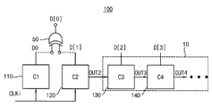
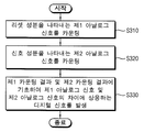
도 1은 본 발명의 일 실시예에 따른 카운터 회로를 나타내는 블록도이고, 도 34는 본 발명의 일 실시예에 따른 카운팅 방법을 나타내는 순서도이다.FIG. 1 is a block diagram illustrating a counter circuit according to an embodiment of the present invention, and FIG. 34 is a flowchart illustrating a counting method according to an embodiment of the present invention.
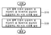
도 1 및 도 34를 참조하면, 카운터 회로(100)는 제1 카운팅 유닛(110) 및 제2 카운팅 유닛(120)을 포함한다. 카운터 회로(100)는 카운팅 결과에 해당하는 디지털 신호의 비트수에 따라서 리플 카운터(ripple counter)(10)를 더 포함할 수 있다.Referring to Figures 1 and 34, the
제1 카운팅 유닛(110)은 입력 클록 신호(CLKi)의 상승 에지 및 하강 에지 중 제1 에지(예를 들어, 하강 에지)에 응답하여 토글링(toggling)하는 제1 비트 신호(D0)를 발생한다(단계 S110). 제2 카운팅 유닛(120)은 입력 클록 신호(CLKi)의 상승 에지 및 하강 에지 중 제2 에지(예를 들어, 상승 에지)에 응답하여 토글링하는 제2 비트 신호(D[1])를 발생한다(단계 S120). 리플 카운터(10)는 제2 카운팅 유닛(120)의 출력 신호(OUT2)에 응답하여 토글링하는 상위 비트 신호들(D[2], D[3])을 발생할 수 있다. 제2 카운팅 유닛(120)의 출력 신호(OUT2)는 후술하는 바와 같이 카운터 회로(100)의 구성에 따라서 제2 비트 신호(D[1]) 또는 제2 비트 신호(D[1])의 반전 신호(/D[1]) 중 하나일 수 있다.The
일 실시예에서, 제1 카운팅 유닛(110)은 입력 클록 신호(CLKi)의 상승 에지 및 하강 에지 중 제1 에지에 응답하여 제1 비트 신호(D0)를 발생하고, 제2 카운팅 유닛(120)은 입력 클록 신호(CLKi)의 상승 에지 및 하강 에지 중 제2 에지에 응답하여 제2 비트 신호(D[1])를 발생할 수 있다. 이와 같이 서로 다른 에지에 응답하여 상보적으로 토글링 동작을 수행함으로써, 제1 비트 신호(D0)와 제2 비트 신호(D[1])가 90도의 위상차를 갖도록 할 수 있다.In one embodiment, the
도 1에는 설명의 편의상 리플 카운터(10)에 포함된 두 개의 카운팅 유닛, 즉 제3 카운팅 유닛(130) 및 제4 카운팅 유닛(140)만을 도시하였으나 리플 카운터(10)에 포함된 카운팅 유닛들(130, 140)의 개수는 디지털 신호, 즉 이진 코드(binary code)(D[0:n])의 비트수에 따라 변경될 수 있다. 이하에서는 설명의 편의상 카운터 회로(100)가 4비트의 디지털 신호(D0, D[1], D[2], D[3]), 즉 이진 코드(D[0:3])를 발생하는 것을 중심으로 카운터 회로(100)의 구성 및 동작을 설명하기로 한다.1 shows only two counting units included in the
리플 카운터(10)는 복수의 카운팅 유닛들(130, 140)이 순차적으로 전단의 출력 신호에 의해 토글링하는 캐스케이드 결합된 구성을 갖는다. 즉 제3 카운팅 유닛(130)은 제2 카운팅 유닛(120)의 출력 신호(OUT2)에 응답하여 토글링하고 제4 카운팅 유닛(140)은 제3 카운팅 유닛(130)의 출력 신호(OUT3)에 응답하여 토글링하는 방식에 의해 순차적으로 주기가 배가되는 상위 비트 신호들, 즉 제3 비트 신호(D[2]) 및 제4 비트 신호(D[3])를 발생한다.The
카운터 회로(100)는 제1 비트 신호(D0) 및 제2 비트 신호(D[1])에 기초하여 이진 코드의 최하위 비트 신호(D[0])를 발생하는 코드 변환기(50)를 더 포함할 수 있다. 예를 들어, 코드 변환기(50)는 배타적 논리합 게이트(exclusive-OR gate)로 구현될 수 있다. 제1 내지 제4 비트 신호들(D0, D[1], D[2], D[3])은 완전한 이진 코드가 아닌 중간 형태의 코드를 나타내지만 그 자체로서 유효한 카운팅 값을 표현하며, 필요에 따라 최하위 비트 신호(D[0])를 발생하여 이진 코드(D[0:3])를 얻을 수 있다. 최하위 비트 신호(D[0])는 카운팅 동작의 진행 중에 토글링하는 신호는 아니며, 카운팅 동작이 완료되어 최종 카운팅 값에 상응하는 제1 내지 제4 비트 신호들(D0, D[1], D[2], D[3])의 논리 상태가 결정된 후에 제1 비트 신호(D0)와 제2 비트 신호(D[1])를 논리 연산하여 제공되는 신호이다. 따라서 코드 변환기(50)는 반드시 카운터 회로(100) 내에 포함되어야 하는 것은 아니며, 카운터 회로(100)의 외부, 나아가 카운터 회로(100)가 실장되는 칩의 외부에 구현될 수도 있다.The
본 발명의 카운터 회로(100)는 그 구성에 따라서 업 카운팅(up-counting) 동작 또는 다운 카운팅(down-counting) 동작을 수행할 수 있다. 이하 도 2 내지 도 6을 참조하여 업 카운팅 동작을 수행하는 카운터 회로의 실시예들을 설명하고, 도 7 내지 도 9를 참조하여 다운 카운팅 동작을 수행하는 카운터 회로의 실시예들을 설명한다.The
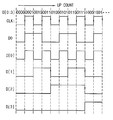
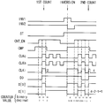
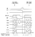
도 2는 도1 의 카운터 회로의 업 카운팅 동작을 나타내는 타이밍도이다.2 is a timing chart showing an up-counting operation of the counter circuit of FIG.
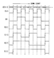
도1 및 도2를 참조하면, 제1 카운팅 유닛(110)에서 발생되는 제1 비트 신호(D0)는 입력 클록 신호(CLKi)의 상승 에지에 응답하여 토글링하고 제2 카운팅 유닛(120)에서 발생되는 제2 비트 신호(D[1])는 입력 클록 신호(CLKi)의 하강 에지에 응답하여 토글링함으로써, 제1 비트 신호(D0)와 제2 비트 신호(D[1])는 90도의 위상차를 갖는다. 리플 카운터(10)에서 발생되는 상위 비트 신호들(D[2], D[3])은 모 두 전단의 출력 신호, 예를 들어, 근접 하위 비트의 하강 에지에 응답하여 토글링한다. 즉, 제3 비트 신호(D[2])는 제2 비트 신호(D[1])의 하강 에지에 응답하여 토글링하고, 제4 비트 신호(D[3])는 제3 비트 신호(D[2])의 하강 에지에 응답하여 토글링한다. 결과적으로 제2 비트 신호(D[1]) 및 상위 비트 신호들(D[2], D[3])은 순차적으로 배가되는 주기를 가지며 이진 코드(D[0:3])의 상위 3비트들을 나타낸다. 이진 코드(D[0:3])의 최하위 비트 신호(D[0])는, 상기 설명한 바와 같이 실제 토글링하는 신호는 아니고, 카운팅이 종료된 후 제1 비트 신호(D0)와 제2 비트 신호(D[1])를 논리 연산하여 발생되는 신호이다. 도 2에는 카운팅 동작의 각각의 종료 시점에서 제1 비트 신호(D0)와 제2 비트 신호(D[1])를 배타적 논리합 연산한 결과(D[0])가 도시되어 있다. 도 2의 상단에는 시간의 경과에 따른 카운팅 동작의 각각의 종료 시점에 대하여 이진 코드(D[0:3])의 값들이 표시되어 있고, 이진 코드(D[0:3])는 0000, 0001, 0010, 0011과 같이 증가하며 결과적으로 업 카운팅 동작이 수행됨을 알 수 있다.1 and 2, the first bit signal D0 generated in the
도 2에 도시된 바와 같이, 본 발명의 일 실시예에 따른 카운터 회로(100)는 입력 클록 신호(CLKi)의 사이클 주기마다 두 번씩 카운팅을 하기 때문에 종래의 카운터와 비교하여 두 배의 동작 속도를 갖는 것을 알 수 있다. 이하에서는 이러한 2배속 카운팅을 DDR(Double Data Rate) 카운팅이라 지칭하고, 이를 수행하는 카운터 회로를 DDR 카운터 회로라 지칭한다. 본 발명의 일 실시예에 따른 DDR 카운터 회로(100)는 종래의 카운터와 비교하여 두 배의 동작 속도를 가지므로 동일한 주기의 클록 신호 및 동일한 카운팅 시간에 대하여 1비트가 증가한 이진 코드를 제공할 수 있으므로, (예를 들어 램프 신호의 기울기를 조절하는 방식에 의해) 더욱 정밀화된 카운팅 값을 제공할 수 있다. 한편 주파수가 반감된 (즉 사이클 주기가 배가된) 클록 신호를 사용하더라도 종래의 리플 카운터와 동일한 시간 내에 동일한 크기의 카운팅 값을 제공할 수 있으므로, 본 발명의 일 실시예에 따른 카운터 회로(100)는 클록 신호의 주파수 감소에 따라 소모 전력을 감소하고, 카운터 회로(100), 이를 포함하는 장치 및 시스템의 동작 마진을 증가할 수 있다.As shown in FIG. 2, the
도 3 및 도 4는 본 발명의 실시예들에 따른 업 카운팅 동작을 수행하는 카운터 회로를 나타내는 회로도이다.Figures 3 and 4 are circuit diagrams illustrating a counter circuit for performing an up-counting operation in accordance with embodiments of the present invention.
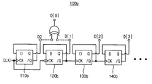
도 3 및 도 4에 도시된 바와 같이, 제1 카운팅 유닛(110), 제2 카운팅 유닛(120) 및 리플 카운터(10)는 제1 비트 신호(D0), 제2 비트 신호(D[1]) 및 상위 비트 신호들(D[2], D[3])을 각각 출력하는 복수의 D-플립플롭들을 포함하여 구현될 수 있다. 제1 카운팅 유닛(110)의 제1 D-플립플롭(110a, 110b) 및 제2 카운팅 유닛(120)의 제2 D-플립플롭(120a, 120b)은 입력 클록 신호(CLKi)의 상승 에지 또는 하강 에지에 대하여 서로 상보적으로 토글링한다. 도 3 및 도 4의 실시예들에서, 제1 D-플립플롭(110a, 110b)은 입력 클록 신호(CLKi)의 상승 에지에 응답하여 토글링하고 제2 D-플립플롭(120a, 120b)은 입력 클록 신호(CLKi)의 하강 에지에 응답하여 토글링한다.3 and 4, the
도 3을 참조하면, 제1 카운팅 유닛(110)은 상승 에지 트리거형(positive-edge triggered) D-플립플롭(110a)을 포함하고 제2 카운팅 유닛(120)은 하강 에지 트리거형 (negative-edge triggered) D-플립플롭(120a)을 포함한다. 리플 카운 터(10)는 상위 비트 신호들(D[2], D[3])을 발생하는 복수의 하강 에지 트리거형 D-플립플롭들(130a, 140a)을 포함한다.3, the
도 4를 참조하면, 도 3의 실시예와 마찬가지로 제1 카운팅 유닛(110)은 상승 에지 트리거형 D-플립플롭(110b)을 포함하고 제2 카운팅 유닛(120)은 하강 에지 트리거형 D-플립플롭(120b)을 포함한다. 리플 카운터(10)는 상위 비트 신호들(D[2], D[3])을 발생하는 복수의 상승 에지 트리거형 D-플립플롭들(130a, 140a)을 포함한다.3, the
도 3의 리플 카운터(10)는 하강 에지 트리거형 D-플립플롭들(130a, 140a)로 구현되고, 전단의 비반전 출력 단자(Q)가 후단의 클록 단자(CK)에 연결된다. 이 경우 제k (k는 2이상의 정수) 카운팅 유닛의 출력 신호(OUTk)는 제k 비트 신호(D[k])에 해당한다. 도 4의 리플 카운터(10)는, 도3의 리플 카운터와는 다르게 상승 에지 트리거형 D-플립플롭들(130b, 140b)로 구현되는 반면에, 전단의 반전 출력 단자(/Q)가 후단의 클록 단자(CK)에 연결된다. 이 경우 제k 카운팅 유닛의 출력 신호(OUTk)는 제k 비트 신호(D[k])의 반전 신호에 해당한다. 결과적으로 도 3 및 도 4의 카운터 회로들(100a, 100b)은 모두 도 2에 도시된 바와 같은 업 카운팅 동작을 수행한다.The ripple counter 10 of FIG. 3 is implemented by falling edge triggered D-
도 5 및 도 6은 토글링 동작을 수행하는 플립플롭들을 나타내는 회로도이다.Figures 5 and 6 are circuit diagrams illustrating flip-flops that perform a toggling operation.
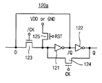
도 5에는 상승 에지 트리거형 D-플립플롭의 일례가 도시되어 있으며, 도 6에는 하강 에지 트리거형 D-플립플롭의 일례가 도시되어 있다. 도 5 및 도 6에 도시된 예들은 본 발명의 카운터 회로(100)에 포함된 D-플립플롭의 동작을 설명하기 위 한 것으로서, 반드시 도 5에 도시된 구성에 한정되는 것은 아니며 각 카운팅 유닛에 포함된 플립플롭들의 구성은 실시예에 따라 변경될 수 있다.FIG. 5 shows an example of a rising edge triggered D-flip flop, and FIG. 6 shows an example of a falling edge triggered D-flip flop. 5 and 6 illustrate the operation of the D-flip-flop included in the
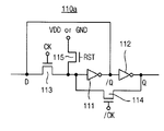
도 5를 참조하면, 상승 에지 트리거형 D-플립플롭(110a)은 제1 인버터(111), 제2 인버터(112), 제1 스위치(113) 및 제2 스위치(114)를 포함한다.Referring to FIG. 5, the rising edge triggered D-
제1 인버터(111)의 출력은 제2 인버터(112)의 입력과 연결되고 제2 스위치(114)를 매개로 하여 제2 인버터(112)의 출력이 제1 인버터(111)의 입력과 연결되는 래치 구조를 갖는다. 도 5의 예에서 제1 인버터(111)의 출력은 반전 출력 단자(/Q)에 해당하고 제2 인버터(112)의 출력은 비반전 출력 단자(Q)에 해당한다. 제1 스위치(113)는 데이터 단자(D)와 제1 인버터(111)의 입력 사이에 연결되고 1 스위치(113)의 제어 단자(CK)는 클록 단자에 해당한다. 제1 스위치(113)의 제어 단자(CK)에는 입력 클록 신호(CLKi)가 인가되고 제2 스위치(114)의 제어 단자(/CK)에는 입력 클록 신호(CLKi)의 반전 신호(/CLKi)가 인가된다.The output of the first inverter 111 is connected to the input of the
상승 에지 트리거형 D-플립플롭(110a)은 저장 상태를 초기화하기 위한 리셋 스위치(115)를 더 포함할 수 있다. 리셋 신호(RST)에 응답하여 리셋 스위치(115)가 턴온되면 리셋 전압(VDD, GND)의 논리 레벨에 따라 반전 출력 단자(/Q) 및 비반전 출력 단자(Q)의 논리 상태가 논리 로우(logic low) 또는 논리 하이(logic high)로 초기화될 수 있다.The rising edge triggered D-flip-
입력 클록 신호(CLKi)가 논리 로우일 때 D-플립플롭(110a)은 메모리, 즉 저장 상태에 있고 데이터 단자(D)의 논리 상태가 변하더라도 플립플롭의 상태는 변하지 않는다. 입력 클록 신호(CLKi)가 논리 하이로 천이할 때, 즉 입력 클록 신 호(CLKi)의 상승 에지에서 비반전 출력 단자(Q)에는 데이터 단자(D)의 논리 상태가 저장된다. 이와 같이 제어 단자(CK)에 인가되는 신호의 에지에 동기하여 논리 상태가 변화하는 플립플롭을 에지 트리거형(edge-triggered)이라고 하고, 도 5의 D-플립플롭(110a)은 상승 에지 트리거형 플립플롭에 해당한다.When the input clock signal CLKi is logic low, the state of the flip-flop does not change even if the logic state of the D-flip-
상승 에지 트리거형 D-플립플롭(110a)은 반전 출력 단자(/Q)가 데이터 단자(D)와 연결되어 토글링 동작을 수행한다. 입력 클록 신호(CLKi)가 하강하여 논리 로우가 되면 제2 스위치(114)가 턴온되어 비반전 출력 단자(Q)와 반대되는 반전 출력 단자(/Q)의 논리 상태가 데이터 단자(D)에 설정되지만 플립플롭의 상태는 변하지 않는다. 입력 클록 신호(CLKi)가 상승하여 논리 하이가 되면 결과적으로 반전 출력 단자(/Q)의 논리 상태가 제1 인버터(111)의 입력에 인가되어 비반전 출력 단자(Q)의 논리 상태가 역전된다. 이와 같이 상승 에지 트리거형 D-플립플롭(110a)은 입력 클록 신호(CLKi)의 상승 에지마다 논리 하이에서 논리 로우로 또는 논리 로우에서 논리 하이로 저장 상태가 역전되는 토글링 동작을 수행한다.The rising edge triggered D-
도 6을 참조하면, 하강 에지 트리거형 D-플립플롭(120a)은 제1 인버터(121), 제2 인버터(122), 제1 스위치(123) 및 제2 스위치(124)를 포함하고, 실시예에 따라서 리셋 스위치(125)를 더 포함할 수 있다.6, the falling edge triggered D-
도 6의 하강 에지 트리거형 D-플립플롭(120a)은 도 5의 상승 에지 트리거형 D-플립플롭(110a)과 유사한 구성을 갖지만, 제1 스위치(123)의 제어 단자(/CK)에 입력 클록 신호(CLKi)의 반전 신호(/CLKi)가 인가되고 제2 스위치(124)의 제어 단자(CK)에 입력 클록 신호(CLKi)가 인가되는 점이 다르다. 즉 도 5와 도 6의 플립플 롭들은 클록 단자들(CK, /CK)이 서로 뒤바뀐 구조를 갖는다.The falling edge triggered D-
입력 클록 신호(CLKi)의 상승 에지에 응답하여 토글링 동작을 수행하는 도 5의 상승 에지 트리거형 플립플롭(110a)과는 반대로 도 6의 하강 에지 트리거형 플립플롭(120a)은 입력 클록 신호(CLKi)의 하강 에지에 응답하여 토글링 동작을 수행한다. 입력 클록 신호(CLKi)가 상승하여 논리 하이가 되면 제2 스위치(124)가 턴온되어 비반전 출력 단자(Q)와 반대되는 반전 출력 단자(/Q)의 논리 상태가 데이터 단자(D)에 설정되지만 플립플롭의 상태는 변하지 않는다. 입력 클록 신호(CLKi)가 하강하여 논리 로우가 되면 반전 출력 단자(/Q)의 논리 상태가 제1 인버터(121)의 입력에 인가되어 비반전 출력 단자(Q)의 논리 상태가 역전된다. 이와 같이 하강 에지 트리거형 D-플립플롭(120a)은 입력 클록 신호(CLKi)의 하강 에지마다 저장 상태가 역전되는 토글링 동작을 수행한다.Contrary to the rising edge triggered
이러한 토글링 동작을 수행하는 플립플롭들을 이용하여 상기 설명한 업 카운팅 동작 또는 후술하는 다운 카운팅 동작을 수행하는 카운터 회로(100)가 구현될 수 있다.The
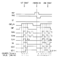
도 7은 도 1의 카운터 회로의 다운 카운팅 동작을 나타내는 타이밍도이다.7 is a timing chart showing a down-counting operation of the counter circuit of FIG.
도 1 및 도 7을 참조하면, 제1 카운팅 유닛(110)에서 발생되는 제1 비트 신호(D0)는 입력 클록 신호(CLKi)의 하강 에지에 응답하여 토글링하고, 제2 카운팅 유닛(120)에서 발생되는 제2 비트 신호(D[1])는 입력 클록 신호(CLKi)의 상승 에지에 응답하여 토글링함으로써 제1 비트 신호(D0)와 제2 비트 신호(D[1])는 90도의 위상차를 갖는다. 리플 카운터(10)에서 발생되는 상위 비트 신호들(D[2], D[3])은 모두 전단의 출력 신호, 예를 들어, 근접 하위 비트의 상승 에지에 응답하여 토글링한다. 즉, 제3 비트 신호(D[2])는 제2 비트 신호(D[1])의 상승 에지에 응답하여 토글링하고, 제4 비트 신호(D[3])는 제3 비트 신호(D[2])의 상승 에지에 응답하여 토글링한다. 결과적으로 제2 비트 신호(D[1]) 및 상위 비트 신호들(D[2], D[3])은 순차적으로 배가되는 주기를 가지며 이진 코드(D[0:3])의 상위 3비트들을 나타낸다. 이진 코드(D[0:3])의 최하위 비트 신호(D[0])는, 상기 설명한 바와 같이 실제 토글링하는 신호는 아니고, 카운팅이 종료된 후 제1 비트 신호(D0)와 제2 비트 신호(D[1])를 논리 연산하여 발생되는 신호이다. 도 7에는 카운팅 동작의 각각의 종료 시점에서 제1 비트 신호(D0)와 제2 비트 신호(D[1])를 배타적 논리합 연산한 결과(D[0])가 도시되어 있다. 도 7의 상단에는 시간의 경과에 따른 카운팅 동작의 각각의 종료 시점에 대하여 이진 코드(D[0:3])의 값들이 표시되어 있고, 이진 코드(D[0:3])는 0000, 1111, 1110, 1101과 같이 감소하며 결과적으로 다운 카운팅 동작이 수행됨을 알 수 있다.1 and 7, the first bit signal D0 generated in the
도 7에 도시된 바와 같이 본 발명의 일 실시예에 따른 카운터 회로(100)는 업 카운팅 동작을 수행하는 경우와 마찬가지로 입력 클록 신호(CLKi)의 사이클 주기마다 두 번씩 카운팅을 하기 때문에 종래의 카운터와 비교하여 두 배의 동작 속도를 갖는 것을 알 수 있다.As shown in FIG. 7, the
도 8 및 도 9는 본 발명의 실시예들에 따른 다운 카운팅 동작을 수행하는 카운터 회로를 나타내는 회로도이다.Figures 8 and 9 are circuit diagrams illustrating a counter circuit that performs a down-counting operation in accordance with embodiments of the present invention.
도 8 및 도 9에 도시된 바와 같이, 제1 카운팅 유닛(110), 제2 카운팅 유 닛(120) 및 리플 카운터(10)는 제1 비트 신호(D0), 제2 비트 신호(D[1]) 및 상위 비트 신호들(D[2], D[3])을 각각 출력하는 복수의 D-플립플롭들을 포함하여 구현될 수 있다. 제1 카운팅 유닛(110)의 제1 D-플립플롭(110c, 110d) 및 제2 카운팅 유닛(120)의 제2 D-플립플롭(120d, 120d)은 입력 클록 신호(CLKi)의 상승 에지 또는 하강 에지에 대하여 서로 상보적으로 토글링한다. 도 8 및 도 9의 실시예들에서, 제1 D-플립플롭(110c, 110d)은 입력 클록 신호(CLKi)의 하강 에지에 응답하여 토글링하고 제2 D-플립플롭(120c, 120d)은 입력 클록 신호(CLKi)의 상승 에지에 응답하여 토글링한다.8 and 9, the
도 8을 참조하면, 제1 카운팅 유닛(110)은 하강 에지 트리거형 D-플립플롭(110c)을 포함하고 제2 카운팅 유닛(120)은 상승 에지 트리거형 D-플립플롭(120c)을 포함한다. 리플 카운터(10)는 상위 비트 신호들(D[2], D[3])을 발생하는 복수의 상승 에지 트리거형 D-플립플롭들(130c, 140c)을 포함한다.8, the
도 9를 참조하면, 도 8의 실시예와 마찬가지로 제1 카운팅 유닛(110)은 상승 에지 트리거형 D-플립플롭(110d)을 포함하고 제2 카운팅 유닛(120)은 하강 에지 트리거형 D-플립플롭(120d)을 포함한다. 리플 카운터(10)는 상위 비트 신호들(D[2], D[3])을 발생하는 복수의 하강 에지 트리거형 D-플립플롭들(130d, 140d)을 포함한다.8, the
도 8의 리플 카운터(10)는 상승 에지 트리거형 D-플립플롭들(130c, 140c)로 구현되고, 전단의 비반전 출력 단자(Q)가 후단의 클록 단자(CK)에 연결된다. 이 경우 제k (k는 2이상의 정수) 카운팅 유닛의 출력 신호(OUTk)는 제k 비트 신호(D[k]) 에 해당한다. 도 9의 리플 카운터(10)는, 도8의 리플 카운터와는 다르게 하강 에지 트리거형 D-플립플롭들(130d, 140d)로 구현되는 반면에, 전단의 반전 출력 단자(/Q)가 후단의 클록 단자(CK)에 연결된다. 이 경우 제k 카운팅 유닛의 출력 신호(OUTk)는 제k 비트 신호(D[k])의 반전 신호에 해당한다. 결과적으로 도 8 및 도 9의 카운터 회로들(100c, 100d)은 모두 도 7에 도시된 바와 같은 다운 카운팅 동작을 수행한다.The ripple counter 10 of FIG. 8 is implemented as rising edge triggered D-
상기 설명한 바와 같이, 상승 에지 트리거형 D-플립플롭 및 하강 에지 트리거형 D-플립플롭은 도 5 및 도 6과 동일 또는 유사한 구성으로 구현될 수 있다.As described above, the rising edge triggered D-flip-flop and the falling edge triggered D-flip flop can be implemented in the same or similar configuration as in Figs. 5 and 6.
도 10은 종래의 카운터 회로와 본 발명의 실시예들에 따른 카운터 회로의 카운팅 동작을 나타내는 타이밍도이다.10 is a timing chart showing the counting operation of the conventional counter circuit and the counter circuit according to the embodiments of the present invention.
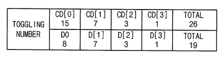
도 10을 참조하면, 종래의 카운터는 입력 클록 신호(CLKi)의 16번의 사이클 주기에 걸쳐 0000부터 1111까지의 값을 카운팅하는 비트 신호들(CD[0], CD[1], CD[2], CD[4])을 발생한다. 반면에 본 발명의 실시예들에 따른 DDR 카운터(100)는 입력 클록 신호(CLKi)의 사이클 주기마다 두 번씩 카운팅을 하기 때문에 입력 클록 신호(CLKi)의 8번의 사이클 주기에 걸쳐 0000부터 1111까지의 값을 카운팅할 수 있다. 따라서 본 발명의 실시예들에 따른 DDR 카운터 회로(100)는 종래의 카운터와 비교하여 두 배의 동작 속도를 가지며, 클록 주파수가 반감된 입력 클록 신호(CLKi)를 사용하더라도 종래의 카운터와 동일한 시간 내에 동일한 카운팅 값을 제공할 수 있다. 본 발명의 일 실시예에 따른 DDR 카운터 회로(100)는 클록 신호의 주파수 감소에 따라 소모 전력을 감소하고, 카운터 회로(100), 이를 포함하는 장치 및 시스템의 동작 마진을 향상시킬 수 있다.Referring to FIG. 10, the conventional counter includes the bit signals CD [0], CD [1], and CD [2] that count values from 0000 to 1111 over 16 cycles of the input clock signal CLKi. , CD [4]). On the other hand, since the
도 11은 종래의 카운터 회로와 본 발명의 실시예들에 따른 카운터 회로의 토글링 회수를 나타낸다.11 shows the number of toggling of a conventional counter circuit and a counter circuit according to embodiments of the present invention.
도 11에는, 도 10에 나타낸 0000부터 1111까지 카운팅 동작을 수행하는 경우에 대하여, 종래의 카운터 회로와 본 발명의 실시예들에 따른 카운터 회로(100)의 각 비트 신호들의 토글링 회수가 기재되어 있다.11, the number of toggling of each bit signal of the
도 11을 참조하면, 본 발명의 일 실시예에 따른 DDR 카운터(100)의 제1 비트 신호(D0)의 토글링 회수는 8회로서, 종래의 카운터의 최하위비트 신호(CD[0])의 토글링 회수인 15회에 비하여 반감된 것을 알 수 있다. 이와 같이, 본 발명의 일 실시예에 따른 DDR 카운터(100)는 클록 신호의 주파수의 감소에 따라 소모 전력을 감소할 수 있을 뿐만 아니라, 동일한 주파수의 클록 신호를 이용하는 경우에도 토글링 빈도수가 가장 많은 제1 비트 신호(D0)의 토글링 회수를 반감함으로써 소모 전력을 더욱 감소할 수 있다.11, the number of toggling of the first bit signal D0 of the
도 12는 본 발명의 일 실시예에 따른 카운터 회로를 포함하는 아날로그-디지털 컨버터를 나타내는 회로도이고, 도 35는 본 발명의 일 실시예에 따른 아날로그-디지털 변환 방법을 나타내는 순서도이다.FIG. 12 is a circuit diagram showing an analog-to-digital converter including a counter circuit according to an embodiment of the present invention, and FIG. 35 is a flowchart showing an analog-to-digital conversion method according to an embodiment of the present invention.
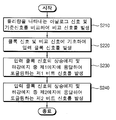
도 12를 참조하면, 본 발명의 일 실시예에 따른 아날로그-디지털 변환 방법을 수행하는 아날로그-디지털 컨버터(200)는 비교기(210), 클록 입력 회로(220) 및 카운터 회로(100e)를 포함한다.12, an analog-to-
비교기(210)는 물리량을 나타내는 아날로그 신호(ANLG) 및 기준 신호(REF)를 비교하여 비교 신호(CMP)를 발생한다(단계 S210). 아날로그 신호(ANLG)는 빛의 세기, 음향의 세기, 시간 등과 같은 유효한 임의의 물리량을 나타낼 수 있으며, 예를 들어, 상기 물리량은 아날로그 신호(ANLG)의 전압 레벨에 상응할 수 있다. 이 경우, 아날로그 신호(ANLG)의 전압 레벨을 비교하기 위하여 기준 신호(REF)는 일정한 기울기를 갖고 상승 또는 하강하는 램프(ramp) 신호로 제공될 있다. 비교기(210)는 아날로그 신호(ANLG)의 전압 레벨과 기준 신호(REF), 즉 램프 신호의 전압 레벨을 비교하여, 전압 레벨이 동일하게 되는 시점에서 천이하는 비교 신호(CMP)를 발생할 수 있다. 결과적으로 아날로그 신호(ANLG)의 전압 레벨이 나타내는 물리량은 비교 신호(CMP)의 천이 시점, 즉 시간량으로 표현된다.The
클록 입력 회로(220)는 클록 신호(CLK) 및 비교 신호(CMP)에 기초하여 입력 클록 신호(CLKi)를 발생한다(단계 S220). 예를 들어, 클록 입력 회로(220)는 도 12에 나타낸 바와 같이 논리곱 게이트로 구현될 수 있다. 이 경우, 클록 입력 회로(220)는 비교 신호(CMP)가 논리 하이를 유지하는 동안에는 클록 신호(CLK)를 입력 클록 신호(CLKi)로서 출력하고 비교 신호(CMP)가 논리 로우로 천이하는 시점에서 입력 클록 신호(CLKi)를 비활성화시켜 카운터 회로(100e)의 카운팅 동작을 종료하도록 한다.The
카운터 회로(100e)는 입력 클록 신호(CLKi)를 카운팅하여 아날로그 신호(ANLG)에 상응하는 디지털 신호(D0, D[1]), D[2], D[3])를 발생한다. 도 12에는 업 카운팅 동작을 수행하는 카운터 회로(100e)를 예시하였으나, 도 1 내지 도 11을 참조하여 설명한 바와 같이, 카운터 회로는 다운 카운팅 동작을 수행하도록 구현될 수도 있다. 카운터 회로(100e)는 제1 카운팅 유닛(110e) 및 제2 카운팅 유닛(120e)을 포함하고, 카운팅 결과에 해당하는 디지털 신호의 비트수에 따라서 리플 카운터(130e, 140e)를 더 포함할 수 있다. 제1 카운팅 유닛(110e)은 입력 클록 신호(CLKi)의 상승 에지 및 하강 에지 중 제1 에지에 응답하여 토글링하는 제1 비트 신호(D0)를 발생하고(단계 S230), 제2 카운팅 유닛(120e)은 입력 클록 신호(CLKi)의 상승 에지 및 하강 에지 중 제2 에지에 응답하여 토글링하는 제2 비트 신호(D[1])를 발생한다(단계 S240). 리플 카운터(130e, 140e)는 제2 비트 신호(D[1]) 또는 제2 비트 신호(D[1])의 반전 신호에 응답하여 토글링하는 상위 비트 신호들(D[2], D[3])을 발생할 수 있다.The
도 12에는 설명의 편의상 업 카운팅 동작을 수행하는 카운터 회로(100e)의 구성의 일례를 도시하였으나, 상기 설명한 바와 같이 카운터 회로(100e)는 업 카운팅 동작 또는 다운 카운팅 동작을 수행하기 위하여 다양하게 변형될 수 있다. 제1 카운팅 유닛(110e), 제2 카운팅 유닛(120e) 및 리플 카운터(130e, 140e)는 제1 비트 신호(D0), 제2 비트 신호(D[1]) 및 상위 비트 신호들(D[2], D[3])을 각각 출력하는 복수의 D-플립플롭들을 포함하고, 제1 카운팅 유닛(110e)의 제1 D-플립플롭 및 제2 카운팅 유닛(120e)의 제2 D-플립플롭은 입력 클록 신호(CLKi)의 상승 에지 또는 하강 에지에 대하여 서로 상보적으로 토글링한다.Although an example of the configuration of the
도 14는 도 12의 카운터 회로의 동작을 나타내는 타이밍도이다.14 is a timing chart showing the operation of the counter circuit of Fig.
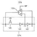
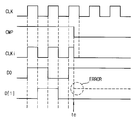
도 14를 참조하면, 카운터 회로(100e)의 기본적인 동작은 도 1의 카운터 회로(100)와 동일하다. 예를 들어, 도 14에 도시된 바와 같이, 제1 카운팅 유닛(110e)에서 발생되는 제1 비트 신호(D0)는 입력 클록 신호(CLKi)의 상승 에지에 응답하여 토글링하고 제2 카운팅 유닛(120e)에서 발생되는 제2 비트 신호(D[1])는 입력 클록 신호(CLKi)의 하강 에지에 응답하여 토글링한다. 리플 카운터(130e, 140e)에서 발생되는 상위 비트 신호들(D[2], D[3])은 편의상 도시를 생략하였다. Referring to Fig. 14, the basic operation of the
비교 신호(CMP)에 기초하여 입력 클록 신호(CLKi)가 비활성화되는 도 12에 도시된 구성에서는 카운팅 동작의 종료 시점(te)을 나타내는 비교 신호(CMP)의 하강 에지가 입력 클록 신호(CLKi)의 하강 에지를 유발하여 카운팅 동작의 종료 시점(te)에서 제2 비트 신호(D[1])가 불필요하게 토글링하는 에러(ERROR)가 발생될 수 있다. 카운터 회로(100e)의 제2 카운팅 유닛(120e)은 카운팅 동작의 종료 시점(te)을 나타내는 비교 신호(CMP)에 응답하여 상기 제2 비트 신호의 토글링을 중단하도록 구현될 수 있다. 카운팅 동작의 종료 시점(te)에서의 토글링 중단을 위하여, 도 12에 도시된 바와 같이, 제2 카운터 유닛(120e)은 입력 클록 신호(CLKi)에 응답하여 토글링 동작을 수행하는 D-플립플롭(121e)과 피드백 스위치(122e)를 포함하여 구현될 수 있다. 이하 도 13을 참조하여 제2 카운팅 유닛의 구성 및 동작을 설명하기로 한다.In the configuration shown in Fig. 12 in which the input clock signal CLKi is inactivated on the basis of the comparison signal CMP, the falling edge of the comparison signal CMP indicating the ending point te of the counting operation is the input clock signal CLKi An erroneous error ERROR may be generated in which a falling edge is caused to unnecessarily toggle the second bit signal D [1] at the ending point te of the counting operation. The
도 13은 도 12의 카운터 회로에 포함된 제2 카운팅 유닛을 나타내는 회로도이다.13 is a circuit diagram showing a second counting unit included in the counter circuit of Fig.
도 13을 참조하면, 제2 카운팅 유닛(120e)은 제2 D-플립플롭(121e) 및 피드백 스위치(122e)를 포함한다. 제2 D-플립플롭(121e)은 제1 인버터(121), 제2 인버터(122) 및 제1 스위치(123)를 포함한다. 피드백 스위치(122e)는 비교 신호(CMP)에 응답하여 제2 D-플립플롭(121e)의 반전 출력 단자(/Q) 또는 비반전 출력 단자(Q)를 제2 D-플립플롭(121e)의 데이터 단자(D)에 선택적으로 연결한다.Referring to FIG. 13, the
비교 신호(CMP)가 제1 논리 상태(예를 들어, 논리 하이)일 때 피드백 스위치(122e)는 제1 인버터(121)의 출력인 반전 출력 단자(/Q)를 데이터 단자(D)와 연결하고, 이 경우 제2 카운팅 유닛(120e)은 토글링 동작을 수행한다. 제1 스위치(123)의 제어 단자(/CK)에는 입력 클록 신호(CLKi)의 반전 신호(/CLKi)가 인가되고, 입력 클록 신호(CLKi)가 상승하여 논리 하이가 되더라도 D-플립플롭(121e)의 저장 상태는 변하지 않는다. 입력 클록 신호(CLKi)가 하강하여 논리 로우가 되면 반전 출력 단자(/Q)의 논리 상태가 제1 인버터(121)의 입력에 인가되어 비반전 출력 단자(Q)의 논리 상태가 역전된다. 이와 같이 반전 출력 단자(/Q)가 데이터 단자(D)와 피드백 연결된 경우에는, 하강 에지 트리거형 D-플립플롭(121e)은 입력 클록 신호(CLKi)의 하강 에지마다 저장 상태가 역전되는 토글링 동작을 수행한다. The
비교 신호(CMP)가 제2 논리 상태(예를 들어, 논리 로우)일 때 피드백 스위치(122e)는 제2 인버터(121)의 출력인 비반전 출력 단자(Q)를 데이터 단자(D)와 연결하고, 이 경우 제2 카운팅 유닛(120e)은 토글링 동작을 중단하고 저장 상태를 유지한다. 도 14에 도시된 바와 같이, 카운팅 동작의 종료 시점(te)을 나타내는 비교 신호(CMP)의 하강 에지에서 입력 클록 신호(CLKi)가 천이하더라도 데이터 단자(D)와 비반전 출력 단자(Q)의 논리 상태는 동일하므로 제2 카운팅 유닛(122e)은 토글링 동작을 중단한다. 따라서 제2 비트 신호(D[1])는 카운팅 동작의 종료 시점(te)에서 토글링하지 않고 입력 클록 신호(CLKi)의 마지막 하강 에지에서 토글링된 논 리 상태를 유지한다.The
도 15는 본 발명의 일 실시예에 따른 아날로그-디지털 컨버터를 포함하는 장치를 나타내는 블록도이다.15 is a block diagram illustrating an apparatus including an analog-to-digital converter in accordance with an embodiment of the present invention.
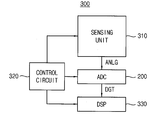
도 15를 참조하면, 장치(300)는 감지부(310), 아날로그-디지털 컨버터(200) 및 제어 회로(320)를 포함한다.Referring to FIG. 15, the
감지부(310)는 물리량을 감지하여 상기 물리량에 상응하는 아날로그 신호(ANLG)를 발생한다. 아날로그-디지털 컨버터(200)는 적어도 하나의 카운터 회로를 이용하여 아날로그 신호(ANLG)를 기준 신호와 비교하여 아날로그 신호(ANLG)에 상응하는 디지털 신호(DGT)를 발생한다. 제어 회로(320)는 감지부(310) 및 아날로그-디지털 컨버터(200)의 동작 타이밍을 제어한다.The
아날로그-디지털 컨버터(200)는, 상기 설명한 바와 같이 본 발명의 일 실시예에 따른 제1 카운팅 유닛 및 제2 카운팅 유닛을 포함하고, 카운팅 결과에 해당하는 디지털 신호의 비트수에 따라서 리플 카운터를 더 포함하는 적어도 하나의 DDR 카운터 회로를 포함하여 데이터 변환 동작을 수행한다. DDR 카운팅 동작을 위하여 제1 카운팅 유닛은 입력 클록 신호의 상승 에지 및 하강 에지 중 제1 에지에 응답하여 토글링하는 제1 비트 신호를 발생하고, 제2 카운팅 유닛은 입력 클록 신호의 상승 에지 및 하강 에지 중 제2 에지에 응답하여 토글링하는 제2 비트 신호를 발생한다. 리플 카운터는 제2 비트 신호 또는 제2 비트 신호의 반전 신호에 응답하여 토글링하는 상위 비트 신호들을 발생한다. As described above, the analog-to-
감지부(310)는 빛의 세기, 음향의 세기, 시간 등과 같은 유효한 임의의 물리 량을 감지하여 이를 전기적인 신호인 아날로그 신호(ANLG)로 변환하여 출력하고, 이러한 감지부(310)를 포함하는 장치(300)는 전하 결합 소자 (Charge Coupled Device) 이미지 센서 및 시모스 (CMOS; Complementary Metal Oxide Semiconductor) 이미지 센서와 같은 이미지 센서, 이를 포함하는 디지털 카메라, 소음 측정기, 컴퓨팅 시스템 등과 같은 다양한 전자 장치 및 시스템일 수 있다. 실시예에 따라서, 장치(300)는 디지털 신호(DGT)를 수신하여 이를 처리하는 디지털 신호 프로세서(DSP; Digital Signal Processor)(330)를 더 포함할 수 있으며, 디지털 신호 프로세서(330)는 장치(300)의 외부에 구현될 수도 있다.The
본 발명의 일 실시예에 따른 아날로그-디지털 컨버터(200)를 포함하는 장치(300)는 적어도 하나의 DDR 카운터 회로를 이용하여, 동작 속도를 증가시키고 소모 전력을 감소시킬 수 있다.The
이하에서는, 본 발명의 일 실시예에 따른 카운터 회로를 이용하여 구현될 수 있는 다양한 전자 장치 중에서 이미지 센서 및 상관 이중 샘플링 방법에 대하여 더욱 상세히 설명하기로 한다.Hereinafter, an image sensor and a correlated double sampling method among various electronic devices that can be implemented using a counter circuit according to an embodiment of the present invention will be described in more detail.
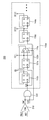
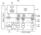
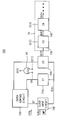
도 16 및 도 17은 본 발명의 일 실시예에 따른 공통의 카운터 회로를 포함하는 이미지 센서를 나타내는 블록도이다.Figures 16 and 17 are block diagrams illustrating an image sensor including a common counter circuit in accordance with an embodiment of the present invention.
도 16을 참조하면, 이미지 센서(400)는 픽셀 어레이(410), 드라이버/어드레스 디코더(420), 제어 회로(430), 램프 신호 발생기(440), 상관 이중 샘플링부(450), 비교부(460), 및 래치부(470)를 포함하여 구현될 수 있다.16, the
영상 기기 분야에서, 물리량으로서 입사광을 감지하는 CCD형 혹은 CMOS형 이 미지 센서가 촬상 장치로서 사용되고 있으며, 도 16의 이미지 센서(400)는 이러한 CCD 이미지 센서 또는 CMOS 이미지 센서일 수 있다. In the field of imaging devices, a CCD type or CMOS type image sensor that detects incident light as a physical quantity is used as an imaging device, and the
픽셀 어레이(410)는 단위 구성 요소(예를 들어, 단위 화소(pixel))에 의해 입사광을 전기적인 아날로그 신호로 변환하여 출력하기 위하여 배열된 복수의 픽셀들을 포함한다. APS(Active Pixel Sensor) 또는 게인 셀(gain cell)이라고 지칭되는 이미지 센서에서는 단위 화소의 배열을 포함하는 화소부에 대하여 어드레스 제어를 하여 임의로 선택된 개개의 단위 화소로부터 신호가 판독되도록 하고 있다. APS는 어드레스 제어형의 촬상 장치의 일례라 할 수 있으며, 드라이버/어드레스 디코더(420)는 행 및/또는 열 단위로 픽셀 어레이의 동작을 제어하기 위하여 구비된다. 제어 회로(430)는 이미지 센서(400)의 각 구성 요소의 동작 타이밍을 제어하기 위한 제어 신호들을 발생한다.The
픽셀 어레이(410)로부터 판독된 아날로그의 화소 신호는, 비교부(460), 래치부(470), 카운터 회로(100) 등으로 구현된 아날로그-디지털 컨버터에 의해 디지털 신호로 변환된다. 화소 신호는 일반적으로 칼럼(column)) 단위로 출력되어 처리되며 이를 위하여 상관 이중 샘플링부(450), 비교부(460), 및 래치부(470)는 각각 칼럼 단위로 구비된 복수의 CDS 회로(451)들, 비교기(461)들 및 래치(471)들을 포함할 수 있다.The analog pixel signals read from the
픽셀 어레이(410)로부터 출력되는 아날로그 신호는 각 화소마다 리셋 성분(또는 오프셋 성분)에 편차가 있기 때문에 리셋 성분에 따른 신호 전압과 신호 성분에 따른 신호 전압의 차를 취함으로써 유효한 신호 성분을 추출할 필요가 있다. 이와 같이 화소를 초기화하였을 때의 리셋 성분 및 신호 성분(즉 이미지 신호 성분)을 구하고 그 차이를 유효한 신호 성분으로 추출하는 것을 상관 이중 샘플링(CDS; Correlated Double Sampling)이라고 한다.Since the analog signal output from the
상관 이중 샘플링부(450)는 캐패시터, 스위치 등을 이용하여 리셋 성분을 나타내는 아날로그 전압과 포토다이오드 등을 통하여 감지된 신호 성분을 나타내는 아날로그 전압의 차이를 구하여 아날로그 더블 샘플링(ADS; Analog Double Sampling)을 수행하고 유효한 신호 성분에 상응하는 아날로그 전압을 출력한다. 비교부(460)는 상관 이중 샘플링부(450)로부터 칼럼 단위로 출력되는 아날로그 전압과 램프 신호 발생기(440)로부터 발생되는 램프 신호를 비교하여 유효한 신호 성분에 따른 각각의 천이 시점을 갖는 비교 신호들을 칼럼 단위로 출력한다. 카운터 회로(100)에서 출력되는 비트 신호들(D0, D[1], D[2], D[3])은 각각의 래치(471)에 공통으로 제공되며, 래치부(470)는 각 비교 신호의 천이 시점에 응답하여 카운터 회로(100)로부터 출력되는 비트 신호들(D0, D[1], D[2], D[3])을 래치하고, 래치된 디지털 신호를 칼럼 단위로 출력한다.The correlated
카운터 회로(100)는 본 발명의 일 실시예에 따른 DDR 동작을 수행하는 카운터 회로로 구현된다. 상기 설명한 바와 같이, 카운터 회로(100)는 제1 카운팅 유닛 및 제2 카운팅 유닛을 포함한다. DDR 카운팅 동작을 위하여 제1 카운팅 유닛은 입력 클록 신호의 상승 에지 및 하강 에지 중 제1 에지에 응답하여 토글링하는 제1 비트 신호(D0)를 발생하고, 제2 카운팅 유닛은 입력 클록 신호의 상승 에지 및 하강 에지 중 제2 에지에 응답하여 토글링하는 제2 비트 신호(D[1])를 발생한다. 카 운팅 결과에 해당하는 디지털 신호의 비트수에 따라서 부가될 수 있는 리플 카운터는 제2 비트 신호(D[1]) 또는 제2 비트 신호(D[1])의 반전 신호에 응답하여 토글링하는 상위 비트 신호들(D[2], D[3])을 발생한다.The
종래의 카운터와 비교하여 두 배의 동작 속도를 가지는 DDR 카운터 회로(100)를 이용하여 아날로그-디지털 변환 동작을 수행함으로써, 이미지 센서(400)는 향상된 동작 속도 및 동작 마진을 갖고 소모 전력을 감소시킬 수 있다.By performing the analog-to-digital conversion operation using the
도 16을 참조하여 본 발명의 일 실시예에 따른 DDR 카운터 회로가 아날로그 더블 샘플링을 수행하는 이미지 센서(400)에 이용되는 것을 설명하였으나, 도 17 및 도 18을 참조하여 후술하는 바와 같이 DDR 카운터 회로는 디지털 더블 샘플링(DDS; Digital Double Sampling)을 수행하는 이미지 센서에도 이용될 수 있다. 디지털 더블 샘플링은 화소를 초기화하였을 때의 리셋 성분에 대한 아날로그 신호 및 신호 성분에 대한 아날로그 신호를 각각 디지털 신호로 변환한 후에 두 개의 디지털 신호의 차이를 유효한 신호 성분으로 추출하는 것을 말한다.16, a DDR counter circuit according to an embodiment of the present invention is used in an
도 16의 이미지 센서(400)와 비교하여 도 17의 이미지 센서(500)의 래치부(570)는 디지털 더블 샘플링을 수행하기 위한 구성을 갖는다. 칼럼 단위로 구비된 각각의 래치(571)는 제1 래치(572) 및 제2 래치(573)를 포함한다. 픽셀 어레이(510)는 상관 이중 샘플링을 위한 리셋 성분을 나타내는 제1 아날로그 신호 및 이미지 신호 성분을 나타내는 제2 아날로그 신호를 순차적으로 출력한다. 제1 샘플링 과정에서 비교부(560)는 리셋 성분을 나타내는 제1 아날로그 전압과 램프 신호 발생기(440)로부터 발생되는 램프 신호를 비교하여 리셋 성분에 따른 각각의 천이 시점을 갖는 비교 신호들을 칼럼 단위로 출력한다. 카운터 회로(100)에서 출력되는 비트 신호들(D0, D[1], D[2], D[3])은 각각의 래치(571)에 공통으로 제공되며, 각각의 래치(571)는 각 비교 신호의 천이 시점에 응답하여 카운터 회로(100)로부터 출력되는 비트 신호들(D0, D[1], D[2], D[3])을 래치하여 리셋 성분에 관한 디지털 신호를 제1 래치(572)에 저장한다. 제2 샘플링 과정에서 비교부(560)는 이미지 신호 성분을 나타내는 제2 아날로그 전압과 램프 신호 발생기(440)로부터 발생되는 램프 신호를 비교하여 이미지 신호 성분에 따른 각각의 천이 시점을 갖는 비교 신호들을 칼럼 단위로 출력한다. 래치부(570)는 각 비교 신호의 천이 시점에 응답하여 카운터 회로(100)로부터 출력되는 비트 신호들(D0, D[1], D[2], D[3])을 래치하여 이미지 신호 성분에 관한 디지털 신호를 제2 래치(573)에 저장한다. 제1 래치(572) 및 제2 래치(573)에 저장된 디지털 신호들은 논리 연산을 수행하는 내부 회로에 제공되어 유효한 이미지 신호 성분을 나타내는 값들이 계산되고, 이와 같은 방식으로 디지털 더블 샘플링이 수행될 수 있다.Compared with the
카운터 회로(100)는 본 발명의 일 실시예에 따른 DDR 동작을 수행하는 카운터 회로로 구현된다. 상기 설명한 바와 같이, 카운터 회로(100)는 제1 카운팅 유닛 및 제2 카운팅 유닛을 포함한다. DDR 카운팅 동작을 위하여 제1 카운팅 유닛은 입력 클록 신호의 상승 에지 및 하강 에지 중 제1 에지에 응답하여 토글링하는 제1 비트 신호(D0)를 발생하고, 제2 카운팅 유닛은 입력 클록 신호의 상승 에지 및 하강 에지 중 제2 에지에 응답하여 토글링하는 제2 비트 신호(D[1])를 발생한다. 카운팅 결과에 해당하는 디지털 신호의 비트수에 따라서 부가될 수 있는 리플 카운터 는 제2 비트 신호(D[1]) 또는 제2 비트 신호(D[1])의 반전 신호에 응답하여 토글링하는 상위 비트 신호들(D[2], D[3])을 발생한다.The
종래의 카운터와 비교하여 두 배의 동작 속도를 가지는 DDR 카운터 회로(100)를 이용하여 아날로그-디지털 변환 동작을 수행함으로써, 이미지 센서(400)는 향상된 동작 마진을 갖고 소모 전력을 감소시킬 수 있다. 아날로그 더블 샘플링을 수행하는 도 16의 이미지 센서(400)와 비교하여, 도 17의 이미지 센서(500)는 디지털 더블 샘플링을 수행하기 때문에 하나의 유효한 이미지 신호 성분을 얻기 위해 두 번의 카운팅 동작을 수행하여야 하고, 따라서 DDR 카운터 회로(100)로부터 발휘되는 이미지 센서(500)의 성능 향상은 더욱 증대됨을 알 수 있다.By performing the analog-to-digital conversion operation using the
도 16 및 도 17을 참조하여 공통의 카운터 회로를 이용하여 상관 이중 샘플링을 수행하는 이미지 센서(400, 500)에 대하여 설명하였으나, 이미지 센서는 고속 동작을 위하여 칼럼 단위로 구비된 복수의 카운터 회로들을 포함하여 구현될 수도 있다. 이하 칼럼 단위로 구비된 복수의 카운터 회로들을 포함하는 이미지 센서와 디지털 더블 샘플링을 수행하기에 적합한 본 발명의 실시예들에 따라 반전 기능 또는 모드 전환 기능을 갖는 DDR 카운터 회로에 대해 설명한다.16 and 17, the
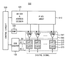
도 18은 본 발명의 일 실시예에 따른 복수의 카운터 회로를 포함하는 이미지 센서를 나타내는 블록도이다.18 is a block diagram illustrating an image sensor including a plurality of counter circuits according to one embodiment of the present invention.
도 18을 참조하면, 이미지 센서(600)는 픽셀 어레이(610), 드라이버/어드레스 디코더(620), 제어 회로(630), 램프 신호 발생기(640), 비교부(660), 및 카운팅부(680)를 포함하여 구현될 수 있다.18, the
픽셀 어레이(610)는 단위 구성 요소(예를 들어, 단위 화소(pixel))에 의해 입사광을 전기적인 아날로그 신호로 변환하여 출력하기 위하여 배열된 복수의 픽셀들을 포함한다. 드라이버/어드레스 디코더(620)는 행 및/또는 열 단위로 픽셀 어레이의 동작을 제어하기 위하여 구비된다. 제어 회로(630)는 이미지 센서(600)의 각 구성 요소의 동작 타이밍을 제어하기 위한 제어 신호(CTRL)를 발생한다. 후술하는 바와 같이, 제어 회로(630)에서 발생되는 제어 신호(CTRL)는 실시예에 따라서 반전 동작을 제어하기 위한 신호들(INV1, INV2) 또는 업/다운 모드 전환 동작을 제어하기 위한 신호들(HD, U/D)을 포함할 수 있다.The
픽셀 어레이(610)로부터 판독된 아날로그의 화소 신호는, 비교부(660) 및 카운팅부(680)로 구현된 아날로그-디지털 컨버터에 의해 디지털 신호로 변환된다. 화소 신호는 칼럼 단위로 출력되어 처리되며 이를 위하여 비교부(660) 및 카운팅부(680)는 각각 칼럼 단위로 구비된 복수의 비교기(661)들 및 복수의 카운터 회로(700)들을 포함할 수 있다. 이와 같이 칼럼 단위로 구비된 복수의 신호 처리 수단을 이용하여 1행분의 화소 신호들을 동시에 병렬적으로 처리함으로써, 이미지 센서(600)는 대역 성능이나 노이즈의 측면에서 향상된 성능을 갖고 고속 동작이 가능하게 된다.The analog pixel signals read out from the
픽셀 어레이(610)는 상관 이중 샘플링을 위한 리셋 성분을 나타내는 제1 아날로그 신호 및 이미지 신호 성분을 나타내는 제2 아날로그 신호를 순차적으로 출력하고, 제1 아날로그 신호 및 제2 아날로그 신호에 기초하여 비교부(660) 및 카운팅부(680)로 구현된 아날로그-디지털 컨버터는 디지털적으로 상관 이중 샘플링, 즉 디지털 더블 샘플링을 수행한다.The
도 36은 본 발명의 일 실시예에 따른 상관 이중 샘플링 방법을 나타내는 순서도이다.36 is a flowchart illustrating a correlated double sampling method according to an embodiment of the present invention.
도 18 및 도 36을 참조하면, 도 18에 도시된 비교부(660) 및 카운팅부(680)로 구현된 아날로그-디지털 컨버터는 리셋 성분을 나타내는 제1 아날로그 신호를 카운팅하고(제1 카운팅 단계 S310), 신호 성분을 나타내는 제2 아날로그 신호를 카운팅한다(제2 카운팅 단계 320). 상기 제1 카운팅 결과 및 상기 제2 카운팅 결과에 기초하여 상기 제1 아날로그 신호 및 상기 제2 아날로그 신호의 차이에 상응하는 디지털 신호가 발생된다(단계 330). 여기서 상기 제1 카운팅 단계 및 상기 제2 카운팅 단계의 각각은 전술한 바와 같은 DDR 카운팅 방식으로 수행된다. 즉 제1 및 제2 카운팅 단계에서, 각각의 카운터 회로(700)는 입력 클록 신호의 상승 에지 및 하강 에지 중 제1 에지에 응답하여 토글링하는 제1 비트 신호를 발생하고(단계 S110), 상기 입력 클록 신호의 상승 에지 및 하강 에지 중 제2 에지에 응답하여 토글링하는 제2 비트 신호를 발생한다(단계 S120). 실시예에 따라서, 상기 제2 비트 신호 또는 상기 제2 비트 신호의 반전 신호에 응답하여 토글링하는 상위 비트 신호들을 발생할 수 있다.18 and 36, the analog-to-digital converter implemented by the comparing
각각의 카운터 회로(700)는 상기 제1 카운팅 결과를 저장하고, 후술하는 바와 같은 반전 동작 또는 업/다운 모드 전환 동작을 수행한 후, 그 결과에 기초하여 제2 카운팅을 수행한다. 따라서 카운팅부(680)에서 최종적으로 출력되는 디지털 신호는 상관 이중 샘플링에 의해 보상된 유효한 이미지 신호에 상응한다.Each
종래의 카운터와 비교하여 두 배의 동작 속도를 가지는 DDR 카운터 회로(700)를 이용하여 상관 이중 샘플링을 수행함으로써, 이미지 센서(600)는 향상된 동작 속도 및 동작 마진을 갖고 소모 전력을 감소시킬 수 있다.By performing correlated double sampling using a
각각의 카운터 회로(700)는 DDR 카운팅 동작을 수행할 뿐 아니라, 전술한 디지털 더블 샘플링을 수행하기 위하여 반전 기능 또는 모드 전환 기능을 갖는다. 이하 본 발명의 실시예들에 따른 반전 기능 또는 모드 전환 기능을 갖는 카운터 회로(700)에 대해 설명한다.Each of the
도 19는 본 발명의 일 실시예에 따른 카운터 회로를 나타내는 블록도이다.19 is a block diagram showing a counter circuit according to an embodiment of the present invention.
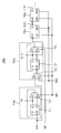
도 19를 참조하면, 카운터 회로(700)는 제1 카운팅 유닛(710), 제2 카운팅 유닛(720), 리플 카운터(70), 클록 제어 회로(750) 및 클록 입력 회로(760)를 포함한다.19, the
전술한 바와 같이, DDR 카운팅 동작을 수행하기 위하여 제1 카운팅 유닛(710) 및 제2 카운팅 유닛(720)은 입력 클록 신호의 상승 에지 또는 하강 에지에 대하여 서로 상보적으로 토글링하는 제1 비트 신호(D0) 및 제2 비트 신호(D[1])를 발생한다. 리플 카운터(10)는 캐스케이드 결합된 복수의 카운팅 유닛들(730, 740)을 포함하고, 제2 카운팅 유닛(720)의 출력 신호(OUT2)에 응답하여 토글링하는 상위 비트 신호들(D[2], D[3])을 발생한다. 제2 카운팅 유닛(720)의 출력 신호(OUT2)는 카운터 회로(700)의 구성에 따라서 제2 비트 신호(D[1]) 또는 제2 비트 신호(D[1])의 반전 신호(/D[1]) 중 하나일 수 있다.As described above, to perform the DDR counting operation, the
도 1의 카운터 회로(100)와 비교하여, 도 19의 카운터 회로(700)는 클록 제 어 회로(750) 및 클록 입력 회로(760)를 더 포함한다. 클록 제어 회로(750)는 제1 비트 신호(D0) 및 제2 비트 신호(D[1])에 기초하여 클록 제어 신호(ST)를 발생하고, 클록 입력 회로(760)는 클록 제어 신호(ST)에 응답하여 입력 클록 신호(CLKi)를 반전한다. 카운터 회로(700)에서 발생되는 제1 및 제2 비트 신호들(D0, D[1])은 최종적인 이진 코드가 아닌 중간 코드를 나타내고, 반전 동작 또는 모드 전환 동작을 포함하는 디지털 이중 샘플링 과정에서 오차가 발생할 수 있다. 따라서 디지털 더블 샘플링 과정에서 정확한 카운팅 값을 제공하기 위하여 제1 카운팅 단계가 완료된 후 제2 카운팅 단계의 개시 전에, 제1 카운팅 결과에 따라서 입력 클록 신호(CLKi)의 반전 여부를 결정할 필요가 있다. 클록 제어 회로(750) 및 클록 입력 회로(760)는 디지털 더블 샘플링 과정에서의 오차를 방지하고 정확한 카운팅 값을 제공하기 위하여 부가된다.Compared with the
도 18의 이미지 센서(600)에서의 디지털 이중 샘플링은 도 20에 도시된 반전 기능을 갖는 카운터 회로(700a) 또는 도 27에 도시된 업/다운 모드 전환 기능을 갖는 카운터 회로(700b)를 이용하여 수행될 수 있다.Digital double sampling in the
도 20은 본 발명의 일 실시예에 따른 반전 기능을 갖는 카운터 회로를 나타내는 회로도이다.20 is a circuit diagram showing a counter circuit having an inverting function according to an embodiment of the present invention.
도 20을 참조하면, 카운터 회로(700a)는 제1 카운팅 유닛(710a) 및 제2 카운팅 유닛(720a)을 포함하며, 실시예에 따라서, 리플 카운터(730a, 740a)를 더 포함할 수 있다. 도 19에 도시된 클록 제어 회로(750) 및 클록 입력 회로(760)는 편의상 도시를 생략하였으며, 이에 대해서는 도 22를 참조하여 후술한다.Referring to Fig. 20, the
제1 카운팅 유닛(710a)은 제1 D-플립플롭(711) 및 제1 멀티플렉서(712)를 포함한다.The
제1 D-플립플롭(711)은 입력 클록 신호(CLKi)의 상승 에지 및 하강 에지 중 제1 에지(예를 들어, 상승 에지)에 응답하여 토글링하는 제1 비트 신호(D0)를 발생한다. 제1 멀티플렉서(712)는 제1 반전 제어 신호(INV1)에 응답하여 제1 D-플립플롭(711)의 반전 출력 단자(/Q) 또는 비반전 출력 단자(Q)를 제1 D-플립플롭(711)의 데이터 단자(D)에 선택적으로 연결한다. 따라서 제1 D-플립플롭(711)은 제1 반전 제어 신호(INV1)가 비활성화(예를 들어, 논리 로우)된 경우에는 반전 출력 단자(/Q)가 데이터 단자(D)에 피드백되어 토글링 동작을 수행하고, 제1 반전 제어 신호(INV1)가 활성화(예를 들어, 논리 하이)된 경우에는 비반전 출력 단자(Q)가 데이터 단자(D)에 피드백되어 입력 클록 신호(CLKi)의 토글링에 무관하게 저장 상태를 유지한다.The first D-
제2 카운팅 유닛(720a)은 제2 D-플립플롭(721), 반전 멀티플렉서(722) 및 피드백 멀티플렉서(723)를 포함한다.The
반전 멀티플렉서(722)는 제1 반전 제어 신호(INV1)에 응답하여 입력 클록 신호(CLKi) 및 제2 반전 제어 신호(INV2) 중 하나를 선택하여 출력한다. 제2 반전 제어 신호(INV2)는 제1 카운팅 동작이 종료된 후 제2 D-플립플롭(721)의 저장 상태, 즉 제2 비트 신호(D[1])를 반전하기 위하여 제1 반전 제어 신호(INV1)가 활성화(예를 들어, 논리 하이)되는 동안에 하나의 에지를 인가하는 방식으로 제공되어 반전 시점을 나타낸다. 제1 및 제2 반전 신호들(INV1, INV2)은 도 18의 이미지 센 서(600)의 동작 타이밍을 제어하는 제어 회로(630)에서 출력되는 제어 신호(CTRL)일 수 있다. 제2 D-플립플롭(721)은 반전 멀티플렉서(722)의 출력에 응답하여 토글링 동작을 수행한다. 제2 D-플립플롭(721)은 통상의 카운팅 동작시 입력 클록 신호(CLKi)의 상승 에지 및 하강 에지 중 제2 에지(예를 들어, 하강 에지)에 응답하여 토글링하는 제2 비트 신호(D[1])를 발생한다. 상기 설명한 바와 같이, 제1 D-플립플롭(711)과 제2 D-플립플롭(721) 중 하나는 상승 에지 트리거형이고 다른 하나는 하강 에지 트리거형으로 구현되어 제1 비트 신호(D0)와 제2 비트 신호(D[1])는 90도의 위상차를 가질 수 있다. 피드백 멀티플렉서(723)는 도 13의 피드백 스위치(122e)와 동일한 기능을 수행하기 위한 것이며 중복된 설명은 생략하기로 한다.The
복수의 유닛들(730a, 740a)을 포함하는 리플 카운터는 제2 카운팅 유닛(720a)의 출력 신호(OUT2)에 응답하여 토글링하는 상위 비트 신호들(D[2], D[3])을 발생한다. 리플 카운터에 포함되는 제3 카운팅 유닛(730a), 제4 카운팅 유닛(740a) 등 복수의 카운팅 유닛들은 동일한 구성을 가지고 캐스케이드 결합될 수 있으며, 이하 도 21을 참조하여 제3 카운팅 유닛(730a)에 대해서 설명하기로 한다.The ripple counter including the plurality of
도 21은 도 20의 제3 카운팅 유닛의 일례를 나타내는 회로도이다.21 is a circuit diagram showing an example of the third counting unit in Fig.
도 21을 참조하면, 제3 카운팅 유닛(730a)은 제3 D-플립플롭(731) 및 반전 멀티플렉서(732)를 포함한다.21, the
반전 멀티플렉서(732)는 제1 반전 제어 신호(INV1)에 응답하여 전단의 출력 신호, 즉 제2 카운팅 유닛(720a)의 출력 신호(OUT2) 및 제2 반전 제어 신호(INV2) 중 하나를 선택하여 출력한다. 제2 카운팅 유닛(720a)에 포함된 반전 멀티플렉 서(722)와 제3 카운팅 유닛(730a)에 포함된 반전 멀티플렉서(732)는 각각의 D-플립플롭(721, 731)에 대하여 실질적으로 동일한 반전 동작을 수행하고, 이러한 복수의 멀티플렉서들은 반전 제어 신호(INV1, INV2)에 응답하여 제2 비트 신호(D[1]) 및 상위 비트 신호들(D[2], D[3])을 반전하기 위한 반전 제어부를 형성한다. 제3 D-플립플롭(731)은 통상의 카운팅 동작시 전단의 출력 신호(OUT2)에 응답하여 토글링하는 제3 비트 신호(D[2])를 발생한다. 도 21에는 제3 D-플립플롭(731)이 하강 에지 트리거형으로 구현되고, 출력 신호(OUT3)가 제3 비트 신호(D[2])에 해당하는 실시예가 도시되어 있으나, 상기 설명한 바와 같이, 카운팅 유닛들의 구성에 따라서 제3 D-플립플롭(731)이 상승 에지 트리거형으로 구현되고, 출력 신호(OUT3)가 제3 비트 신호(D[2])의 반전 신호에 해당하도록 구현될 수 있다.The inverting
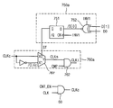
도 22는 본 발명의 일 실시예에 따른 반전 기능을 갖는 카운터 회로에 포함된 클록 제어 회로 및 클록 입력 회로의 일례를 나타내는 회로도이다.22 is a circuit diagram showing an example of a clock control circuit and a clock input circuit included in a counter circuit having an inverting function according to an embodiment of the present invention.
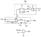
도 22를 참조하면, 클록 제어 회로(750a)는 제1 비트 신호(D0) 및 제2 비트 신호(D[1])에 기초하여 클록 제어 신호(ST)를 발생하고, 클록 입력 회로(760a)는 클록 제어 신호(ST)에 응답하여 입력 클록 신호(CLKi)를 반전한다.22, the
클록 제어 회로(750a)는 논리 게이트(752) 및 D-플립플롭(751)을 포함하여 구현될 수 있다. 논리 게이트(752)는 제1 비트 신호(D0) 및 제2 비트 신호(D[1])를 논리 연산하여 출력한다. 예를 들어, 논리 게이트(752)는 제1 반전 신호(INV1)에 응답하여 인에이블되는 배타적 NOR 게이트(exclusive-NOR gate)일 수 있으며, 이 경우 논리 게이트의 출력은 최하위 비트 신호(D[0])의 반전 신호(/D[0])에 해당한 다.The
D-플립플롭(751)은 데이터 단자(D)에 논리 게이트(752)의 출력이 인가되고 클록 단자(CK)에 인가되는 제1 반전 제어 신호(INV1)에 응답하여 클록 제어 신호(ST)를 출력한다. 결과적으로, 제1 반전 제어 신호(INV1)가 활성화되는 동안에 도 20의 카운터 회로(700a)의 반전 동작이 수행되고, 클록 제어 신호(ST)의 논리 레벨은 제1 카운팅 동작이 종료된 후의 제1 비트 신호(D0) 및 제2 비트 신호(D[1])의 논리 레벨에 따라 결정된다.The D flip-
클록 입력 회로(760a)는 멀티플렉서(761) 및 논리곱 게이트(762)를 포함하여 구현될 수 있다. 멀티플렉서(761)는 클록 제어 신호(ST)에 응답하여 클록 신호(CLKc) 또는 반전 클록 신호(/CLKc)를 선택하여 출력한다. 논리곱 게이트(762)는 멀티플렉서(761)의 출력 신호(CLKm) 및 카운팅 동작의 종료 시점을 나타내는 비교 신호(CMP)를 논리 연산하여 입력 클록 신호(CLKi)를 출력한다. 결과적으로 클록 제어 신호(ST)의 논리 레벨에 따라서 클록 신호(CLKc) 또는 반전 클록 신호(/CLKc) 중 하나가 입력 클록 신호(CLKi)로서 출력된다. 클록 신호(CLKc)는 후술하는 바와 같은 카운트 인에이블 신호(CNT_EN)에 의해 활성화되는 신호일 수 있다. 도 22에 함께 도시한 논리곱 게이트(60)는 도 18의 제어 회로(630)에 포함될 수 있으며, 카운트 인에이블 신호(CNT_EN)가 예를 들어 논리 하이로 활성화된 경우에만 클록 신호(CLKc)를 활성화한다.
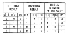
도 23은 도 20의 카운터 회로의 반전 기능에 의한 카운팅 동작을 설명하기 위한 도면이고, 도 24 및 도 25는 도 20의 카운터 회로의 반전 기능에 의한 카운팅 동작을 나타내는 타이밍도이다.FIG. 23 is a view for explaining the counting operation by the inverting function of the counter circuit of FIG. 20, and FIGS. 24 and 25 are timing charts showing the counting operation by the inverting function of the counter circuit of FIG.
상기 설명한 바와 같이, 디지털 더블 샘플링(DDS; Digital Double Sampling)은 화소를 초기화하였을 때의 리셋 성분에 대한 제1 아날로그 신호 및 신호 성분(즉 영상 성분)에 대한 제2 아날로그 신호를 각각 디지털 신호로 변환한 후 두 개의 디지털 신호의 차이를 유효한 신호 성분으로 추출하는 것을 말한다. As described above, Digital Double Sampling (DDS) converts a first analog signal for a reset component when a pixel is initialized and a second analog signal for a signal component (i.e., image component) into a digital signal And then extracts the difference between the two digital signals as a valid signal component.
도 24 및 도 25를 참조하면, 도 20의 반전 기능을 갖는 카운터 회로(700a)는, 리셋 성분에 대한 제1 아날로그 신호를 디지털 신호로 카운팅하는 제1 카운팅 동작(1ST COUNT), 상기 제1 카운팅 결과를 반전시키는 반전 동작(INVERSION), 및 상기 반전 동작에 의한 결과에 기초하여 신호 성분에 대한 제2 아날로그 신호를 디지털 신호로 카운팅하는 제2 카운팅 동작(2ND COUNT)에 의해 디지털 더블 샘플링을 수행한다.Referring to FIGS. 24 and 25, the
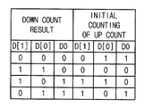
제1 카운팅 동작의 결과, 반전 결과 및 제2 카운팅 동작에서의 첫 번째 카운팅의 각각에 대하여, 제1 비트 신호(D0), 제 2 비트 신호(D[0]) 및 최하위 비트 신호(D[0])의 값들이 도 23에 도시되어 있다. 최하위 비트 신호(D[0])는 디지털 신호를 이진 코드로 변환하였을 때의 최하위 비트를 나타내며, 제1 비트 신호(D0) 및 제 2 비트 신호(D[1])를 배타적 논리합 연산한 결과에 해당한다.The first bit signal D0, the second bit signal D [0] and the least significant bit signal D [0] for each of the inversion result and the first counting in the second counting operation as a result of the first counting operation, ]) Are shown in Fig. The least significant bit signal D [0] represents the least significant bit when the digital signal is converted into a binary code and the exclusive OR operation of the first bit signal D0 and the second bit signal D [1] .
본원 발명의 일 실시예에 따른 DDR 카운터 회로(100, 700)에서 발생되는 제1 비트 신호(D0) 및 제2 비트 신호(D[1])는 이진 코드의 하위 2비트를 그대로 표현하는 것이 아니므로, 제1 카운팅 동작의 결과를 단순히 반전하여 제1 카운팅 동작을 수행하는 경우에는 오차가 발생할 수 있다. 이러한 오차를 방지하기 위하여, 도 20 에 도시된 바와 같이, 제1 카운팅 유닛(710a)은 반전 멀티플렉서를 포함하지 않고 제1 비트 신호(D0)는 제1 카운팅 동작의 결과를 그대로 유지하며, 클록 제어 회로(750a) 및 클록 입력 회로(760a)를 이용하여 제1 카운팅 동작의 결과에 따라서 입력 클록 신호(CLKi)를 반전함으로써, 모든 경우에 대하여 입력 클록 신호(CLKi)의 첫 번째 에지부터 제2 카운팅 동작이 개시되도록 한다.The first bit signal D0 and the second bit signal D [1] generated in the
도 23을 참조하면, 제1 카운팅 동작의 결과에서 최하위 비트 신호(D[0])가 논리 로우(즉, '0')인 경우에는 제2 카운팅 동작에서의 첫 번째 카운팅은 제2 비트 신호(D[1])를 토글링하는 것이어야 하고, 제1 카운팅 동작의 결과에서 최하위 비트 신호(D[0])가 논리 하이(즉, '1')인 경우에는 제2 카운팅 동작에서의 첫 번째 카운팅은 제1 비트 신호(D0)를 토글링하는 것이어야 함을 알 수 있다.23, when the least significant bit signal D [0] is logic low (i.e., '0') in the result of the first counting operation, the first counting in the second counting operation is the second bit signal D [1]) and if the least significant bit signal D [0] in the result of the first counting operation is a logical high (i.e., '1'), then the first It can be seen that the counting should be to toggle the first bit signal D0.
도 24는 제1 카운팅 동작의 결과에서 최하위 비트 신호(D[0])가 논리 로우인 경우에 대한 디지털 더블 샘플링 동작을 나타낸다. 제1 카운팅 동작의 결과에서 최하위 비트 신호(D[0])가 논리 로우인 경우에 도 22의 클록 제어 회로(750a)에서 출력되는 클록 제어 신호(ST)는 제1 반전 제어 신호(INV1)의 상승 에지에 응답하여 논리 로우에서 논리 하이로 천이한다. 제2 카운팅 동작에서는 클록 입력 회로(760a)에 의해서 클록 신호(CLKc)의 반전 신호(/CLKc)가 입력 클록 신호(CLKi)로서 출력되고(즉 입력 클록 신호(CLKi)가 반전되고), 제2 카운팅 동작은 입력 클록 신호(CLKi)의 첫 번째 에지, 즉 하강 에지에서 제2 비트 신호(D[1])를 토글링함으로써 개시된다.FIG. 24 shows a digital double sampling operation for the case where the least significant bit signal D [0] is logic low in the result of the first counting operation. When the least significant bit signal D [0] is logic low in the result of the first counting operation, the clock control signal ST output from the
도 25는 제1 카운팅 동작의 결과에서 최하위 비트 신호(D[0])가 논리 하이인 경우에 대한 디지털 더블 샘플링 동작을 나타낸다. 제1 카운팅 동작의 결과에서 최하위 비트 신호(D[0])가 논리 하이인 경우에 도 22의 클록 제어 회로(750a)에서 출력되는 클록 제어 신호(ST)는 제1 반전 제어 신호(INV1)의 상승 에지가 인가되더라도 논리 로우를 유지한다. 제2 카운팅 동작에서는 클록 입력 회로(760a)에 의해서 클록 신호(CLKc)가 그대로 입력 클록 신호(CLKi)로서 출력되고, 제2 카운팅 동작은 입력 클록 신호(CLKi)의 첫 번째 에지, 즉 상승 에지에서 제1 비트 신호(D0)를 토글링함으로써 개시된다.25 shows a digital double sampling operation for the case where the least significant bit signal D [0] is logic high in the result of the first counting operation. When the least significant bit signal D [0] is logic high in the result of the first counting operation, the clock control signal ST output from the
이와 같이, 클록 제어 회로(750a) 및 클록 입력 회로(760a)를 이용하여, 제1 카운팅 동작이 완료된 후 제2 카운팅 동작의 개시 전에, 제1 비트 신호(D0) 및 제2 비트 신호(D[1])에 기초하여 입력 클록 신호(CLKi)를 반전함으로써, 디지털 더블 샘플링 과정에서의 오차를 방지할 수 있다.As described above, by using the
도 26은 도 20의 반전 기능을 갖는 카운터 회로를 포함하는 이미지 센서의 상관 이중 샘플링 동작을 나타내는 타이밍도이다. 도 26에는 하나의 칼럼에 대한 상관 이중 샘플링 동작이 도시되어 있다.26 is a timing diagram showing a correlated double sampling operation of the image sensor including the counter circuit having the reversal function of FIG. 26 shows a correlated double sampling operation for one column.
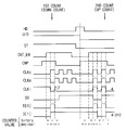
시간 t11에서, 이미지 센서(600)의 제어 회로(630)에서 제공되는 카운트 인에이블 신호(CNT_EN)가 논리 하이로 활성화되고, 인에이블 신호(CNT_EN)에 응답하여 램프 신호 발생기(640)는 램프 신호(RAMP)의 전압 레벨을 감소하기 시작한다. 이로서 카운팅부(680)에 포함된 각각의 카운터 회로(700a)에서는 칼럼 단위로 제1 카운팅 동작이 개시된다. 이 때 화소 전압 신호(Vpix)는 리셋 성분을 나타내는 제1 아날로그 신호로서 비교기(661)에 제공된다.At time t11, the count enable signal CNT_EN provided in the
시간 t12에서, 램프 신호(RAMP)와 화소 전압 신호(Vpix)의 전압 레벨이 동일하게 되고, 비교기(661)에서 출력되는 비교 신호(CMP)는 논리 로우로 천이하여 카운팅 동작이 종료된다. 도 26에는 도시를 생략하였으나, 비교 신호(CMP)에 응답하여 클록 신호(CLKc)에 기초하여 제공되는 입력 클록 신호(CLKi)는 비활성화되고(도 24 및 도 25 참조) 카운터 회로(700a)에는 리셋 성분(Vrst)에 해당하는 제1 카운팅 동작의 결과값(3)이 저장된다.At time t12, the voltage levels of the ramp signal RAMP and the pixel voltage signal Vpix become equal, and the comparison signal CMP output from the
시간 t13에서, 카운트 인에이블 신호(CNT_EN)가 논리 로우로 비활성화되면, 램프 신호 발생기(640)는 디스에이블된다. 시간 t11에서 시간 t13의 구간은 리셋 성분을 카운팅하기 위한 최대 구간을 나타내며 이미지 센서의 특성에 따라 적절한 클록 사이클의 개수에 해당하도록 설정될 수 있다.At time t13, when the count enable signal CNT_EN is deactivated to a logic low, the
시간 t14에서, 제1 반전 제어 신호(INV1)가 논리 하이로 활성화된 동안에 제2 반전 신호(INV2)가 논리 로우로 천이하면, 복수의 반전 멀티플렉서들(722, 732)을 포함하는 반전 제어부는 제2 반전 신호(INV2)의 하강 에지를 제2 카운팅 유닛(710a) 및 리플 카운터(730a, 740a)에 포함된 D-플립플롭들(721, 731)의 클록 단자에 인가함으로써, 제2 비트 신호(D[1]) 및 상위 비트 신호들(D[2], D[3])이 반전된다. 카운터 회로(700a)에는 반전 동작의 결과값(-4)이 저장된다. 상기 설명한 바와 같이, 제1 반전 제어 신호(INV1)의 상승 에지에 응답하여, 클록 제어 회로(750a) 및 클록 입력 회로(760a)는 제2 카운팅 동작을 위하여 입력 클록 신호(CLKi)의 반전 여부를 결정할 수 있다.At time t14, when the second inversion signal INV2 transits to a logic low while the first inversion control signal INV1 is activated to a logic high, the inversion control section including the plurality of
시간 t15에서, 카운트 인에이블 신호(CNT_EN)가 논리 하이로 다시 활성화되 고, 인에이블 신호(CNT_EN)에 응답하여 램프 신호 발생기(640)는 램프 신호(RAMP)의 전압 레벨을 감소하기 시작하고, 각각의 카운터 회로(700a)에서는 칼럼 단위로 제2 카운팅 동작이 개시된다. 이 때 화소 전압 신호(Vpix)는 이미지 신호 성분을 나타내는 제2 아날로그 신호로서 비교기(661)에 제공된다.At time t15 the count enable signal CNT_EN is activated again to a logic high and in response to the enable signal CNT_EN the
시간 t16에서, 램프 신호(RAMP)와 화소 전압 신호(Vpix)의 전압 레벨이 동일하게 되고, 비교기(661)에서 출력되는 비교 신호(CMP)는 논리 로우로 천이하여 제2 카운팅 동작이 종료된다. 비교 신호(CMP)에 응답하여 클록 신호(CLKc)에 기초하여 제공되는 입력 클록 신호(CLKi)는 비활성화되고(도 24 및 도 25 참조), 최종적으로 카운터 회로(700a)에는 리셋 성분(Vrst=3)을 나타내는 제1 아날로그 신호 및 이미지 신호 성분(Vrst+Vsig=7)을 나타내는 제2 아날로그 신호의 차이에 상응하는 디지털 값(Vsig-1=3)이 저장되고, 디지털 값(Vsig-1)은 제1 비트 신호(D0), 제2 비트 신호(D[1]) 및 상위 비트 신호들(D[2], D[3])로 표현되는 디지털 신호로서 출력된다. 유효한 이미지 신호 성분(Vsig)과 카운터 회로(700a)의 최종 출력값(Vsig-1) 사이에는 반전 동작에 기인한 1만큼의 차이가 존재하지만, 이러한 차이는 모든 칼럼에 대해 공통되며 디지털 신호 처리기(DSP) 등의 후속 신호 처리 과정에서 상쇄될 수 있다.At time t16, the voltage levels of the ramp signal RAMP and the pixel voltage signal Vpix become equal, and the comparison signal CMP output from the
시간 t17에서, 카운트 인에이블 신호(CNT_EN)가 논리 로우로 비활성화되면, 램프 신호 발생기(640)는 디스에이블된다. 시간 t15에서 시간 t17의 구간은 이미지 신호 성분을 카운팅하기 위한 최대 구간을 나타내며 이미지 센서의 특성에 따라 적절한 클록 사이클의 개수에 해당하도록 설정될 수 있다.At time t17, when the count enable signal CNT_EN is deactivated to a logic low, the
이와 같이, 반전 기능을 갖는 카운터 회로(700a)를 이용하여 이미지 센서(600)는 디지털적으로 상관 이중 샘플링을 수행할 수 있다. 반전 기능을 갖는 DDR 카운터 회로(700a)를 이용함으로써, 이미지 센서(600)는 동작 속도의 증가에 따라 동작 마진을 향상시키고 소모 전력을 감소할 수 있다. 또한 반전 기능을 갖는 카운터 회로(700a)는 디지털 더블 샘플링 과정에서의 오차를 방지하고 정밀한 카운팅 값을 제공할 수 있는 구성을 부가하여 구비함으로써 이를 포함하는 이미지 센서(600)의 성능이 향상될 수 있다.In this manner, the
도 27은 본 발명의 일 실시예에 따른 모드 전환 기능을 갖는 카운터 회로를 나타내는 회로도이다.27 is a circuit diagram showing a counter circuit having a mode switching function according to an embodiment of the present invention.
도 27을 참조하면, 카운터 회로(700b)는 제1 카운팅 유닛(710b), 제2 카운팅 유닛(720b) 및 리플 카운터(730b, 740b)를 포함한다. 도 19에 도시된 클록 제어 회로(750) 및 클록 입력 회로(760)는 편의상 도시를 생략하였으며, 이에 대해서는 도 29를 참조하여 후술한다.27, the
제1 카운팅 유닛(710b)은 제1 D-플립플롭(715) 및 제1 멀티플렉서(716)를 포함한다.The
제1 D-플립플롭(715)은 입력 클록 신호(CLKi)의 상승 에지 및 하강 에지 중 제1 에지(예를 들어, 상승 에지)에 응답하여 토글링하는 제1 비트 신호(D0)를 발생한다. 제1 멀티플렉서(716)는 제1 모드 제어 신호(HD)에 응답하여 제1 D-플립플롭(715)의 반전 출력 단자(/Q) 또는 비반전 출력 단자(Q)를 제1 D-플립플롭(715)의 데이터 단자(D)에 선택적으로 연결한다. 예를 들어, 제1 D-플립플롭(715)은 제1 모 드 제어 신호(HD)가 논리 로우인 경우에는 반전 출력 단자(/Q)가 데이터 단자(D)에 피드백되어 토글링 동작을 수행하고, 제1 모드 제어 신호(HD)가 논리 하이인 경우에는 비반전 출력 단자(Q)가 데이터 단자(D)에 피드백되어 입력 클록 신호(CLKi)의 토글링에 무관하게 저장 상태를 유지한다.The first D-flip-
제2 카운팅 유닛(720b)은 제2 D-플립플롭(725), 출력 멀티플렉서(726), 피드백 멀티플렉서(727), 및 논리합 게이트(OR gate)(728)를 포함한다. The
제2 D-플립플롭(725)은 입력 클록 신호(CLKi)의 상승 에지 및 하강 에지 중 제2 에지(예를 들어, 하강 에지)에 응답하여 토글링하는 제2 비트 신호(D[1])를 발생한다. 상기 설명한 바와 같이, 제1 D-플립플롭(715)과 제2 D-플립플롭(725) 중 하나는 상승 에지 트리거형으로 다른 하나는 하강 에지 트리거형으로 구현되어 제1 비트 신호(D0)와 제2 비트 신호(D[1])는 90도의 위상차를 가질 수 있다. The second D-flip-
출력 멀티플렉서(726)는 제2 모드 제어 신호(U/D)에 응답하여 제2 D-플립플롭(725)의 비반전 출력 단자(Q)의 신호 또는 반전 출력 단자(/Q)의 신호 중 하나를 출력 신호(OUT2)로서 선택하여, 제2 카운팅 유닛(720b)의 후단에 해당하는 제3 카운팅 유닛(730b)으로 출력한다. 예를 들어, 제2 모드 제어 신호(U/D)가 논리 하이일때는 제2 D-플립플롭(725)의 반전 출력 단자(/Q)의 신호가 출력 신호(OUT2)가 되고, 도 9에서 설명한 바와 같이, 제2 카운팅 유닛(720b) 및 리플 카운터(730b, 740b)는 다운 카운팅 동작을 수행한다. 제2 모드 제어 신호(U/D)가 논리 로우일때는 제2 D-플립플롭(725)의 비반전 출력 단자(Q)의 신호가 출력 신호(OUT2)가 되고, 도 3에서 설명한 바와 같이, 제2 카운팅 유닛(720b) 및 리플 카운터(730b, 740b)는 업 카운팅 동작을 수행한다. The
논리합 게이트(728)는 카운팅 동작의 종료 시점을 나타내는 비교 회로(CMP)의 반전 신호 및 제1 모드 제어 신호(HD)를 논리 연산하여 출력한다. 비교 신호(CMP)가 논리 로우이거나 제1 모드 신호(HD)가 논리 하이일 때 논리합 게이트(728)의 출력은 논리 하이가 되고, 나머지 경우는 논리 로우가 된다. 피드백 멀티플렉서(727)는 논리합 게이트(728)의 출력에 응답하여 제2 D-플립플롭(725)의 반전 출력 단자(/Q) 또는 비반전 출력 단자(Q)를 제2 D-플립플롭(725)의 데이터 단자(D)에 선택적으로 연결한다. 예를 들어, 제2 D-플립플롭(725)은 논리합 게이트(728)의 출력이 논리 로우인 경우에는 반전 출력 단자(/Q)가 데이터 단자(D)에 피드백되어 토글링 동작을 수행하고, 논리합 게이트(728)의 출력이 논리 하이인 경우에는 비반전 출력 단자(Q)가 데이터 단자(D)에 피드백되어 입력 클록 신호(CLKi)의 토글링에 무관하게 저장 상태를 유지한다. 논리합 게이트(728)는 도 13과 관련하여 설명한 카운팅 종료 시점에서의 에러 방지 및 모드 반전 동작시의 에러 방지를 모두 구현하기 위한 것이다. 실시예에 따라서 논리합 게이트(728)는 생략될 수 있으며, 제1 모드 신호(HD)가 피드백 멀티플렉서(727)의 제어를 위하여 제공될 수 있다.The OR
복수의 유닛들(730b, 740b)을 포함하는 리플 카운터는 제2 카운팅 유닛(720b)의 출력 신호(OUT2)에 응답하여 토글링하는 상위 비트 신호들(D[2], D[3])을 발생한다. 리플 카운터에 포함되는 제3 카운팅 유닛(730b), 제4 카운팅 유닛(740b) 등 복수의 카운팅 유닛들은 동일한 구성을 가지고 캐스케이드 결합될 수 있으며, 이하 도 28을 참조하여 제3 카운팅 유닛(730b)에 대해서 설명하기로 한다.The ripple counter including the plurality of
도 28은 도 27의 제3 카운팅 유닛의 일례를 나타내는 회로도이다.28 is a circuit diagram showing an example of the third counting unit in Fig.
도 28을 참조하면, 제3 카운팅 유닛(730b)은 제3 D-플립플롭(735), 출력 멀티플렉서(736) 및 피드백 멀티플렉서(737)를 포함한다.28, the
출력 멀티플렉서(736)는 제2 모드 제어 신호(U/D)에 응답하여 제3 D-플립플롭(735)의 비반전 출력 단자(Q)의 신호 또는 반전 출력 단자(/Q)의 신호 중 하나를 출력 신호(OUT3)로서 선택하여, 제3 카운팅 유닛(730b)의 후단에 해당하는 제4 카운팅 유닛(740b)으로 출력한다. 도 28의 제3 카운팅 유닛(730b)에 포함된 출력 멀티플렉서(736)는 도 27의 제2 카운팅 유닛(720b)에 포함된 출력 멀티플렉서(726)와 동일한 구성이며, 이와 같은 복수의 출력 멀티플렉서들(726, 736)은 카운터 회로(730b)의 업 카운팅 동작 또는 다운 카운팅 동작을 제어하는 모드 전환 제어부를 형성한다. 결과적으로, 제2 모드 제어 신호(U/D)에 응답하여, 모드 전환 제어부는 전단의 비반전 출력 단자(Q)의 신호 또는 전단의 반전 출력 단자(/Q)의 신호 중 하나를 선택하여 후단으로 출력함으로써, 카운터 회로(730b)의 업 카운팅 동작 또는 다운 카운팅 동작을 제어한다.The
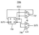
예를 들어, 제2 모드 제어 신호(U/D)가 논리 하이일때는 제2 D-플립플롭(725)의 반전 출력 단자(/Q)의 신호가 출력 신호(OUT2)가 되고, 도 9에서 설명한 바와 같이, 제2 카운팅 유닛(720b) 및 리플 카운터(730b, 740b)는 다운 카운팅 동작을 수행한다. 제2 모드 제어 신호(U/D)가 논리 로우일때는 제2 D-플립플롭(725)의 비반전 출력 단자(Q)의 신호가 출력 신호(OUT2)가 되고, 도 3에서 설명한 바와 같이, 제2 카운팅 유닛(720b) 및 리플 카운터(730b, 740b)는 업 카운팅 동작을 수행한다. For example, when the second mode control signal U / D is logic high, the signal of the inverted output terminal / Q of the second D flip-
피드백 멀티플렉서(737)는 제1 모드 제어 신호(HD)에 응답하여 제3 D-플립플롭(735)의 반전 출력 단자(/Q) 또는 비반전 출력 단자(Q)를 제3 D-플립플롭(735)의 데이터 단자(D)에 선택적으로 연결한다. 예를 들어, 제3 D-플립플롭(735)은 제1 모드 제어 신호(HD)가 논리 로우인 경우에는 반전 출력 단자(/Q)가 데이터 단자(D)에 피드백되어 토글링 동작을 수행하고, 제1 모드 제어 신호(HD)가 논리 하이인 경우에는 비반전 출력 단자(Q)가 데이터 단자(D)에 피드백되어 전단의 출력 신호(OUT2)의 토글링에 무관하게 저장 상태를 유지한다.The
제3 D-플립플롭(735)은 통상의 카운팅 동작시 전단의 출력 신호(OUT2)에 응답하여 토글링하는 제3 비트 신호(D[2])를 발생한다. 도 28에는 제3 D-플립플롭(735)이 하강 에지 트리거형으로 구현된 실시예가 도시되어 있으나, 상기 설명한 바와 같이, 카운팅 유닛들의 구성에 따라서 제3 D-플립플롭(735)이 상승 에지 트리거형으로 구현되고, 출력 신호(OUT3)가 제2 모드 제어 신호(U/D)의 반전 신호에 따라 출력되도록 구현함으로써, 도 28의 구성과 동일하게 업 카운팅 동작 또는 다운 카운팅 동작을 수행할 수 있다.The third D-flip-
도 29는 본 발명의 일 실시예에 따른 모드 전환 기능을 갖는 카운터 회로에 포함된 클록 제어 회로 및 클록 입력 회로의 일례를 나타내는 회로도이다.29 is a circuit diagram showing an example of a clock control circuit and a clock input circuit included in a counter circuit having a mode switching function according to an embodiment of the present invention.
도 29를 참조하면, 클록 제어 회로(750b)는 제1 비트 신호(D0) 및 제2 비트 신호(D[1])에 기초하여 클록 제어 신호(ST)를 발생하고, 클록 입력 회로(760b)는 클록 제어 신호(ST)에 응답하여 입력 클록 신호(CLKi)를 반전한다.29, the
클록 제어 회로(750b)는 논리 게이트(753) 및 D-플립플롭(751)을 포함하여 구현될 수 있다. 논리 게이트(753)는 제1 비트 신호(D0) 및 제2 비트 신호(D[1])를 논리 연산하여 출력한다. 예를 들어, 논리 게이트(752)는 제1 모드 제어 신호(HD)에 응답하여 인에이블되는 배타적 논리합 게이트(exclusive-OR gate)일 수 있으며, 이 경우 논리 게이트의 출력은 최하위 비트 신호(D[0])에 해당한다.The
D-플립플롭(751)은 데이터 단자(D)에 논리 게이트(753)의 출력이 인가되고 클록 단자(CK)에 인가되는 제1 모드 제어 신호(HD)에 응답하여 클록 제어 신호(ST)를 출력한다. 결과적으로, 제1 모드 제어 신호(HD)가 활성화되는 동안에 도 27의 카운터 회로(700b)의 모드 전환 동작이 수행되고, 클록 제어 신호(ST)의 논리 레벨은 제1 카운팅이 종료된 후의 제1 비트 신호(D0) 및 제2 비트 신호(D[1])의 논리 레벨에 따라 결정된다.The D-
클록 입력 회로(760b) 및 논리곱 게이트(60)는 도 22의 클록 입력 회로(760a) 및 논리곱 게이트(60)와 실질적으로 동일하며 중복된 설명은 생략한다.The
도 30은 도 27의 카운터 회로의 모드 전환 기능에 의한 카운팅 동작을 설명하기 위한 도면이고, 도 31 및 도 32는 도 27의 카운터 회로의 모드 전환 기능에 의한 카운팅 동작을 나타내는 타이밍도이다.Fig. 30 is a view for explaining the counting operation by the mode switching function of the counter circuit of Fig. 27, and Figs. 31 and 32 are timing diagrams showing the counting operation by the mode switching function of the counter circuit of Fig.
상기 설명한 바와 같이, 디지털 더블 샘플링(DDS; Digital Double Sampling)은 화소를 초기화하였을 때의 리셋 성분에 대한 제1 아날로그 신호 및 신호 성분(즉 영상 성분)에 대한 제2 아날로그 신호를 각각 디지털 신호로 변환한 후 두 개 의 디지털 신호의 차이를 유효한 신호 성분으로 추출하는 것을 말한다. As described above, Digital Double Sampling (DDS) converts a first analog signal for a reset component when a pixel is initialized and a second analog signal for a signal component (i.e., image component) into a digital signal And then extracts the difference between the two digital signals as a valid signal component.
도 31 및 도 32를 참조하면, 도 27의 반전 기능을 갖는 카운터 회로(700a)는, 리셋 성분에 대한 제1 아날로그 신호를 디지털 신호로 카운팅하는 제1 카운팅 동작(1ST COUNT), 및 상기 제1 카운팅 동작에 의한 결과에 기초하여 신호 성분에 대한 제2 아날로그 신호를 디지털 신호로 카운팅하는 제2 카운팅 동작(2ND COUNT)에 의해 디지털 더블 샘플링을 수행한다. 예를 들어, 도 31 및 도 32에 도시된 바와 같이, 제1 카운팅 동작은 다운 카운팅 동작이고 제2 카운팅 동작은 업 카운팅 동작일 수 있다.Referring to FIGS. 31 and 32, the
제1 카운팅 동작의 결과 및 제2 카운팅 동작에서의 첫 번째 카운팅의 각각에 대하여, 제1 비트 신호(D0), 제 2 비트 신호(D[0]) 및 최하위 비트 신호(D[0])의 값들이 도 30에 도시되어 있다. 최하위 비트 신호(D[0])는 디지털 신호를 이진 코드로 변환하였을 때의 최하위 비트를 나타내며, 제1 비트 신호(D0) 및 제 2 비트 신호(D[0])를 배타적 논리합 연산한 결과에 해당한다.For each of the result of the first counting operation and the first counting in the second counting operation, the first bit signal D0, the second bit signal D [0] and the least significant bit signal D [0] The values are shown in FIG. The least significant bit signal D [0] represents the least significant bit when a digital signal is converted into a binary code. The least significant bit signal D [0] .
본원 발명의 일 실시예에 따른 DDR 카운터 회로(100, 700)에서 발생되는 제1 비트 신호(D0) 및 제2 비트 신호(D[1])는 이진 코드의 하위 2비트를 그대로 표현하는 것이 아니므로, 제1 카운팅 동작의 결과로부터 단순히 제 2 카운팅 동작을 수행하는 경우 오차가 발생할 수 있다. 이러한 오차를 방지하기 위하여, 클록 제어 회로(750b) 및 클록 입력 회로(760b)를 이용하여 제1 카운팅 동작의 결과에 따라서 입력 클록 신호(CLKi)를 반전함으로써, 모든 경우에 대하여 입력 클록 신호(CLKi)의 첫 번째 에지부터 제2 카운팅 동작이 개시되도록 한다.The first bit signal D0 and the second bit signal D [1] generated in the
도 30을 참조하면, 제1 카운팅 동작의 결과에서 최하위 비트 신호(D[0])가 논리 로우(즉, '0')인 경우에는 제2 카운팅 동작에서의 첫 번째 카운팅은 제1 비트 신호(D0)를 토글링하는 것이어야 하고, 제1 카운팅 동작의 결과에서 최하위 비트 신호(D[0])가 논리 하이(즉, '1')인 경우에는 제2 카운팅 동작에서의 첫 번째 카운팅은 제2 비트 신호(D[1])를 토글링하는 것이어야 함을 알 수 있다.Referring to FIG. 30, if the lowest bit signal D [0] is logic low (i.e., '0') in the result of the first counting operation, the first counting in the second counting operation is the first bit signal D0) and the first counting in the second counting operation should be toggled when the lowest bit signal D [0] is logic high (i.e., '1') in the result of the first counting operation, It should be noted that the 2-bit signal D [1] should be toggled.
도 31은 제1 카운팅 동작의 결과에서 최하위 비트 신호(D[0])가 논리 로우인 경우에 대한 디지털 더블 샘플링 동작을 나타낸다. 제1 카운팅 동작에서는 제2 모드 제어 신호(U/D)가 논리 하이이므로 다운 카운팅이 수행되고, 제2 카운팅 동작에서는 제2 모드 제어 신호(U/D)가 논리 로우로 천이하여 업 카운팅이 수행된다. 제1 카운팅 동작에서는 도 29의 클록 제어 회로(750b)에서 출력되는 클록 제어 신호(ST)가 논리 하이이고 따라서 클록 신호(CLKc)의 반전 신호(/CLKc)가 입력 클록 신호(CLKi)로서 출력된다. 제1 카운팅 동작의 결과에서 최하위 비트 신호(D[0])가 논리 로우인 경우에 클록 제어 신호(ST)는 제1 모드 제어 신호(HD)의 상승 에지에 응답하여 논리 하이에서 논리 로우로 천이한다. 따라서 제2 카운팅 동작에서는 제1 카운팅 동작과는 반대로 클록 신호(CLKc)가 입력 클록 신호(CLKi)로서 출력되고, 제2 카운팅 동작은 입력 클록 신호(CLKi)의 첫 번째 에지, 즉 상승 에지에서 제1 비트 신호(D0)를 토글링함으로써 개시된다.31 shows a digital double sampling operation for the case where the least significant bit signal D [0] is logic low in the result of the first counting operation. In the first counting operation, down-counting is performed because the second mode control signal U / D is logic high, and in the second counting operation, the second mode control signal U / D transits to a logic low state, do. In the first counting operation, the clock control signal ST output from the
도 32는 제1 카운팅 동작의 결과에서 최하위 비트 신호(D[0])가 논리 하이인 경우에 대한 디지털 더블 샘플링 동작을 나타낸다. 제1 카운팅 동작의 결과에서 최하위 비트 신호(D[0])가 논리 하이인 경우에 도 27의 클록 제어 회로(750b)에서 출 력되는 클록 제어 신호(ST)는 제1 모드 제어 신호(HD)의 상승 에지가 인가되더라도 논리 하이를 유지한다. 따라서 제2 카운팅 동작에서는 제1 카운팅 동작과 동일하게 클록 신호(CLKc)의 반전 신호(/CLKc)가 입력 클록 신호(CLKi)로서 출력되고, 제2 카운팅 동작은 입력 클록 신호(CLKi)의 첫 번째 에지, 즉 하강 에지에서 제2 비트 신호(D[1])를 토글링함으로써 개시된다.32 shows a digital double sampling operation for the case where the least significant bit signal D [0] is logic high in the result of the first counting operation. The clock control signal ST output from the
이와 같이, 클록 제어 회로(750b) 및 클록 입력 회로(760b)를 이용하여, 제1 카운팅 동작이 완료된 후 제2 카운팅 동작의 개시 전에, 제1 비트 신호(D0) 및 제2 비트 신호(D[1])에 기초하여 입력 클록 신호(CLKi)를 반전함으로써, 디지털 더블 샘플링 과정에서의 오차를 방지할 수 있다.As described above, by using the
도 33은 도 27의 모드 전환 기능을 갖는 카운터 회로를 포함하는 이미지 센서의 상관 이중 샘플링 동작을 나타내는 타이밍도이다. 도 33에는 하나의 칼럼에 대한 상관 이중 샘플링 동작이 도시되어 있다.33 is a timing diagram showing a correlated double sampling operation of the image sensor including the counter circuit having the mode switching function of FIG. 27; Figure 33 shows a correlated double sampling operation for one column.
시간 t21에서, 이미지 센서(600)의 제어 회로(630)에서 제공되는 카운트 인에이블 신호(CNT_EN)가 논리 하이로 활성화되고, 인에이블 신호(CNT_EN)에 응답하여 램프 신호 발생기(640)는 램프 신호(RAMP)의 전압 레벨을 감소하기 시작한다. 이로서 카운팅부(680)에 포함된 각각의 카운터 회로(700b)에서는 칼럼 단위로 제1 카운팅 동작, 즉 다운 카운팅 동작이 개시된다. 이 때 화소 전압 신호(Vpix)는 리셋 성분을 나타내는 제1 아날로그 신호로서 비교기(661)에 제공된다.At time t21, the count enable signal CNT_EN provided in the
시간 t22에서, 램프 신호(RAMP)와 화소 전압 신호(Vpix)의 전압 레벨이 동일하게 되고, 비교기(661)에서 출력되는 비교 신호(CMP)는 논리 로우로 천이하여 카 운팅 동작이 종료된다. 도 33에는 도시를 생략하였으나, 비교 신호(CMP)에 응답하여 클록 신호(CLKc)에 기초하여 제공되는 입력 클록 신호(CLKi)는 비활성화되고(도 31 및 도 32 참조) 카운터 회로(700b)에는 리셋 성분(Vrst)에 해당하는 제1 카운팅 동작의 결과값(-3)이 저장된다.At time t22, the voltage levels of the ramp signal RAMP and the pixel voltage signal Vpix become equal, and the comparison signal CMP output from the
시간 t23에서, 카운트 인에이블 신호(CNT_EN)가 논리 로우로 비활성화되면, 램프 신호 발생기(640)는 디스에이블된다. 시간 t21에서 시간 t23의 구간은 리셋 성분을 카운팅하기 위한 최대 구간을 나타내며 이미지 센서의 특성에 따라 적절한 클록 사이클의 개수에 해당하도록 설정될 수 있다.At time t23, when the count enable signal CNT_EN is deactivated to a logic low, the
시간 t24에서, 제2 모드 제어 신호(U/D)가 논리 하이에서 논리 로우로 천이하면, 복수의 출력 멀티플렉서들(726, 736)을 포함하는 모드 전환 제어부는 각 카운팅 유닛들의 출력 신호가 제공되는 반전 출력 단자(/Q) 또는 비반전 출력 단자(Q)를 제1 카운팅 동작과 반대로 설정함으로써 모드 전환 동작이 수행된다.At time t24, when the second mode control signal U / D transitions from a logic high to a logic low, the mode switching control section including the plurality of
시간 t25에서, 카운트 인에이블 신호(CNT_EN)가 논리 하이로 다시 활성화되고, 인에이블 신호(CNT_EN)에 응답하여 램프 신호 발생기(640)는 램프 신호(RAMP)의 전압 레벨을 감소하기 시작하고, 각각의 카운터 회로(700b)에서는 칼럼 단위로 제2 카운팅 동작, 즉 업 카운팅 동작이 개시된다. 이 때 화소 전압 신호(Vpix)는 이미지 신호 성분을 나타내는 제2 아날로그 신호로서 비교기(661)에 제공된다.At time t25, the count enable signal CNT_EN is activated again to a logic high, and in response to the enable signal CNT_EN, the
시간 t26에서, 램프 신호(RAMP)와 화소 전압 신호(Vpix)의 전압 레벨이 동일하게 되고, 비교기(661)에서 출력되는 비교 신호(CMP)는 논리 로우로 천이하여 제2 카운팅 동작이 종료된다. 비교 신호(CMP)에 응답하여 클록 신호(CLKc)에 기초하여 제공되는 입력 클록 신호(CLKi)는 비활성화되고(도 31 및 도 32 참조), 최종적으로 카운터 회로(700b)에는 리셋 성분(Vrst=3)을 나타내는 제1 아날로그 신호 및 이미지 신호 성분(Vrst+Vsig=7)을 나타내는 제2 아날로그 신호의 차이에 상응하는 디지털 값(Vsig=4)이 저장되고, 디지털 값(Vsig)은 제1 비트 신호(D0), 제2 비트 신호(D[1]) 및 상위 비트 신호들(D[2], D[3])로 표현되는 디지털 신호로서 출력된다.At time t26, the voltage levels of the ramp signal RAMP and the pixel voltage signal Vpix become equal, and the comparison signal CMP output from the
시간 t27에서, 카운트 인에이블 신호(CNT_EN)가 논리 로우로 비활성화되면, 램프 신호 발생기(640)는 디스에이블된다. 시간 t25에서 시간 t27의 구간은 이미지 신호 성분을 카운팅하기 위한 최대 구간을 나타내며 이미지 센서의 특성에 따라 적절한 클록 사이클의 개수에 해당하도록 설정될 수 있다.At time t27, when the count enable signal CNT_EN is deactivated to a logic low, the
이와 같이, 모드 전환 기능을 갖는 카운터 회로(700b)를 이용하여 이미지 센서(600)는 디지털적으로 상관 이중 샘플링을 수행할 수 있다. 업/다운 모드 전환 기능을 갖는 DDR 카운터 회로(700b)를 이용함으로써, 이미지 센서(600)는 동작 속도의 증가에 따라 동작 마진을 향상시키고 소모 전력을 감소할 수 있다. 또한 모드 전환 기능을 갖는 카운터 회로(700b)는 디지털 더블 샘플링 과정에서의 오차를 방지하고 정밀한 카운팅 값을 제공할 수 있는 구성을 부가하여 구비함으로써 이를 포함하는 이미지 센서(600)의 성능이 향상될 수 있다.In this manner, the
본 발명은 카운터 회로를 포함하는 장치 및 시스템에 유용하게 이용될 수 있다. 특히 본 발명은 빠른 동작 속도 및 낮은 소모 전력을 요하는 이미지 센서, 이를 포함하는 카메라 등의 휴대용 전자 장치 등에 더욱 유용하게 이용될 수 있다.The present invention can be usefully used in an apparatus and a system including a counter circuit. Particularly, the present invention can be more effectively used for an image sensor requiring a high operating speed and low power consumption, a portable electronic device such as a camera including the same, and the like.
상기에서는 본 발명이 바람직한 실시예를 참조하여 설명하였지만, 해당 기술분야의 숙련된 당업자는 하기의 특허청구범위에 기재된 본 발명의 사상 및 영역으로부터 벗어나지 않는 범위 내에서 본 발명을 다양하게 수정 및 변경시킬 수 있음을 이해할 것이다.While the present invention has been described with reference to the preferred embodiments thereof, it will be apparent to those skilled in the art that various modifications and variations can be made in the present invention without departing from the spirit and scope of the invention as defined in the appended claims. It will be understood.
도 1은 본 발명의 일 실시예에 따른 카운터 회로를 나타내는 블록도이다.1 is a block diagram showing a counter circuit according to an embodiment of the present invention.
도 2는 도1 의 카운터 회로의 업 카운팅 동작을 나타내는 타이밍도이다.2 is a timing chart showing an up-counting operation of the counter circuit of FIG.
도 3 및 도 4는 본 발명의 실시예들에 따른 업 카운팅 동작을 수행하는 카운터 회로를 나타내는 회로도이다.Figures 3 and 4 are circuit diagrams illustrating a counter circuit for performing an up-counting operation in accordance with embodiments of the present invention.
도 5 및 도 6은 토글링 동작을 수행하는 플립플롭들을 나타내는 회로도이다.Figures 5 and 6 are circuit diagrams illustrating flip-flops that perform a toggling operation.
도 7은 도 1의 카운터 회로의 다운 카운팅 동작을 나타내는 타이밍도이다.7 is a timing chart showing a down-counting operation of the counter circuit of FIG.
도 8 및 도 9는 본 발명의 실시예들에 따른 다운 카운팅 동작을 수행하는 카운터 회로를 나타내는 회로도이다.Figures 8 and 9 are circuit diagrams illustrating a counter circuit that performs a down-counting operation in accordance with embodiments of the present invention.
도 10은 종래의 카운터 회로와 본 발명의 실시예들에 따른 카운터 회로의 카운팅 동작을 나타내는 타이밍도이다.10 is a timing chart showing the counting operation of the conventional counter circuit and the counter circuit according to the embodiments of the present invention.
도 11은 종래의 카운터 회로와 본 발명의 실시예들에 따른 카운터 회로의 토글링 회수를 나타낸다.11 shows the number of toggling of a conventional counter circuit and a counter circuit according to embodiments of the present invention.
도 12는 본 발명의 일 실시예에 따른 카운터 회로를 포함하는 아날로그-디지털 컨버터를 나타내는 회로도이다.12 is a circuit diagram showing an analog-to-digital converter including a counter circuit according to an embodiment of the present invention.
도 13은 도 12의 카운터 회로에 포함된 제2 카운팅 유닛을 나타내는 회로도이다.13 is a circuit diagram showing a second counting unit included in the counter circuit of Fig.
도 14는 도 12의 카운터 회로의 동작을 나타내는 타이밍도이다.14 is a timing chart showing the operation of the counter circuit of Fig.
도 15는 본 발명의 일 실시예에 따른 아날로그-디지털 컨버터를 포함하는 장치를 나타내는 블록도이다.15 is a block diagram illustrating an apparatus including an analog-to-digital converter in accordance with an embodiment of the present invention.
도 16 및 도 17은 본 발명의 일 실시예에 따른 공통의 카운터 회로를 포함하는 이미지 센서를 나타내는 블록도이다.Figures 16 and 17 are block diagrams illustrating an image sensor including a common counter circuit in accordance with an embodiment of the present invention.
도 18은 본 발명의 일 실시예에 따른 복수의 카운터 회로를 포함하는 이미지 센서를 나타내는 블록도이다.18 is a block diagram illustrating an image sensor including a plurality of counter circuits according to one embodiment of the present invention.
도 19는 본 발명의 일 실시예에 따른 카운터 회로를 나타내는 블록도이다.19 is a block diagram showing a counter circuit according to an embodiment of the present invention.
도 20은 본 발명의 일 실시예에 따른 반전 기능을 갖는 카운터 회로를 나타내는 회로도이다.20 is a circuit diagram showing a counter circuit having an inverting function according to an embodiment of the present invention.
도 21은 도 20의 제3 카운팅 유닛의 일례를 나타내는 회로도이다.21 is a circuit diagram showing an example of the third counting unit in Fig.
도 22는 본 발명의 일 실시예에 따른 반전 기능을 갖는 카운터 회로에 포함된 클록 제어 회로 및 클록 입력 회로의 일례를 나타내는 회로도이다.22 is a circuit diagram showing an example of a clock control circuit and a clock input circuit included in a counter circuit having an inverting function according to an embodiment of the present invention.
도 23은 도 20의 카운터 회로의 반전 기능에 의한 카운팅 동작을 설명하기 위한 도면이다.FIG. 23 is a diagram for explaining the counting operation by the inverting function of the counter circuit of FIG. 20; FIG.
도 24 및 도 25는 도 20의 카운터 회로의 반전 기능에 의한 카운팅 동작을 나타내는 타이밍도이다.24 and 25 are timing charts showing the counting operation by the inverting function of the counter circuit of Fig.
도 26은 도 20의 반전 기능을 갖는 카운터 회로를 포함하는 이미지 센서의 상관 이중 샘플링 동작을 나타내는 타이밍도이다.26 is a timing diagram showing a correlated double sampling operation of the image sensor including the counter circuit having the reversal function of FIG.
도 27은 본 발명의 일 실시예에 따른 모드 전환 기능을 갖는 카운터 회로를 나타내는 회로도이다.27 is a circuit diagram showing a counter circuit having a mode switching function according to an embodiment of the present invention.
도 28은 도 27의 제3 카운팅 유닛의 일례를 나타내는 회로도이다.28 is a circuit diagram showing an example of the third counting unit in Fig.
도 29는 본 발명의 일 실시예에 따른 모드 전환 기능을 갖는 카운터 회로에 포함된 클록 제어 회로 및 클록 입력 회로의 일례를 나타내는 회로도이다.29 is a circuit diagram showing an example of a clock control circuit and a clock input circuit included in a counter circuit having a mode switching function according to an embodiment of the present invention.
도 30은 도 27의 카운터 회로의 모드 전환 기능에 의한 카운팅 동작을 설명하기 위한 도면이다.Fig. 30 is a diagram for explaining the counting operation by the mode switching function of the counter circuit of Fig. 27; Fig.
도 31 및 도 32는 도 27의 카운터 회로의 모드 전환 기능에 의한 카운팅 동작을 나타내는 타이밍도이다.Figs. 31 and 32 are timing charts showing the counting operation by the mode switching function of the counter circuit of Fig.
도 33은 도 27의 모드 전환 기능을 갖는 카운터 회로를 포함하는 이미지 센서의 상관 이중 샘플링 동작을 나타내는 타이밍도이다.33 is a timing diagram showing a correlated double sampling operation of the image sensor including the counter circuit having the mode switching function of FIG. 27;
도 34는 본 발명의 일 실시예에 따른 카운팅 방법을 나타내는 순서도이다.34 is a flowchart illustrating a counting method according to an embodiment of the present invention.
도 35는 본 발명의 일 실시예에 따른 아날로그-디지털 변환 방법을 나타내는 순서도이다.35 is a flowchart showing an analog-digital conversion method according to an embodiment of the present invention.
도 36은 본 발명의 일 실시예에 따른 상관 이중 샘플링 방법을 나타내는 순서도이다.36 is a flowchart illustrating a correlated double sampling method according to an embodiment of the present invention.
<도면의 주요부분에 대한 부호의 설명>Description of the Related Art
100, 700: 카운터 회로 110, 710: 제1 카운팅 유닛100, 700: a
120, 720: 제2 카운팅 유닛 10, 70: 리플 카운터120, 720:
122e: 피드백 스위치 400, 500, 600: 이미지 센서122e:
750: 클록 제어 회로 760: 클록 입력 회로750: clock control circuit 760: clock input circuit
D0: 제1 비트 신호 D[1]: 제2 비트 신호D0: first bit signal D [1]: second bit signal
D[0]: 최하위 비트 신호 D[2], D[3]: 상위 비트 신호들D [0]: least significant bit signal D [2], D [3]: upper bit signals
Claims (26)
Priority Applications (2)
| Application Number | Priority Date | Filing Date | Title |
|---|---|---|---|
| KR1020090011692A KR101621244B1 (en) | 2009-02-13 | 2009-02-13 | Counter Circuit, Device Including the Same, and Counting Method |
| US12/590,830 US7990304B2 (en) | 2009-02-13 | 2009-11-13 | Double data rate (DDR) counter, analog-to-digital converter (ADC) using the same, CMOS image sensor using the same and methods in DDR counter, ADC and CMOS image sensor |
Applications Claiming Priority (1)
| Application Number | Priority Date | Filing Date | Title |
|---|---|---|---|
| KR1020090011692A KR101621244B1 (en) | 2009-02-13 | 2009-02-13 | Counter Circuit, Device Including the Same, and Counting Method |
Publications (2)
| Publication Number | Publication Date |
|---|---|
| KR20100092542A KR20100092542A (en) | 2010-08-23 |
| KR101621244B1 true KR101621244B1 (en) | 2016-05-16 |
Family
ID=42559402
Family Applications (1)
| Application Number | Title | Priority Date | Filing Date |
|---|---|---|---|
| KR1020090011692A KR101621244B1 (en) | 2009-02-13 | 2009-02-13 | Counter Circuit, Device Including the Same, and Counting Method |
Country Status (2)
| Country | Link |
|---|---|
| US (1) | US7990304B2 (en) |
| KR (1) | KR101621244B1 (en) |
Families Citing this family (27)
| Publication number | Priority date | Publication date | Assignee | Title |
|---|---|---|---|---|
| JP4853445B2 (en) * | 2007-09-28 | 2012-01-11 | ソニー株式会社 | A / D conversion circuit, solid-state imaging device, and camera system |
| JP5254140B2 (en) * | 2009-07-14 | 2013-08-07 | 株式会社東芝 | A / D converter and solid-state imaging device including the same |
| KR101647366B1 (en) * | 2009-09-25 | 2016-08-11 | 삼성전자주식회사 | Counter Circuit, Device Including the Same, and Counting Method |
| JP5481221B2 (en) * | 2010-02-08 | 2014-04-23 | パナソニック株式会社 | Solid-state imaging device and AD conversion method |
| JP2012161061A (en) * | 2011-02-03 | 2012-08-23 | Toshiba Corp | Digital filter circuit |
| JP5784377B2 (en) * | 2011-06-14 | 2015-09-24 | オリンパス株式会社 | AD conversion circuit and imaging apparatus |
| US8547267B2 (en) | 2011-11-30 | 2013-10-01 | Taiwan Semiconductor Manufacturing Co., Ltd. | Idle tone suppression circuit |
| JP6019793B2 (en) * | 2012-06-20 | 2016-11-02 | ソニー株式会社 | COUNTER, COUNTING METHOD, AD CONVERTER, SOLID-STATE IMAGING ELEMENT, AND ELECTRONIC DEVICE |
| CN102932103B (en) * | 2012-10-22 | 2016-04-20 | 武汉烽火富华电气有限责任公司 | A kind of message transmission rate adaptive reception method based on digital transformer substation |
| KR102009165B1 (en) * | 2013-01-24 | 2019-10-21 | 삼성전자 주식회사 | Image sensor, multi chip package, and electronic device |
| CN103096003B (en) * | 2013-02-07 | 2016-04-27 | 江苏思特威电子科技有限公司 | Imaging device and formation method thereof |
| KR102002466B1 (en) | 2013-05-20 | 2019-07-23 | 에스케이하이닉스 주식회사 | Digital counter |
| KR101996491B1 (en) * | 2013-06-14 | 2019-07-05 | 에스케이하이닉스 주식회사 | Double data rate counter, and analog-digital converting apparatus and cmos image sensor thereof using that |
| KR102075093B1 (en) * | 2013-08-14 | 2020-03-03 | 삼성전자주식회사 | Image sensor and analog to digital converter and analog to digital converting method tererof |
| KR102082288B1 (en) * | 2013-12-12 | 2020-02-27 | 에스케이하이닉스 주식회사 | Double data rate counter, and analog-digital converting apparatus and cmos image sensor thereof using that |
| KR102230446B1 (en) * | 2014-07-31 | 2021-03-23 | 에스케이하이닉스 주식회사 | Electronic device and electronic system with the same |
| KR20160017500A (en) * | 2014-08-06 | 2016-02-16 | 에스케이하이닉스 주식회사 | Double data rate counter, and analog-digital converting apparatus and cmos image sensor thereof using that |
| KR102114906B1 (en) | 2014-08-25 | 2020-05-25 | 에스케이하이닉스 주식회사 | digital counter |
| US20160309135A1 (en) | 2015-04-20 | 2016-10-20 | Ilia Ovsiannikov | Concurrent rgbz sensor and system |
| KR20160145217A (en) * | 2015-06-09 | 2016-12-20 | 에스케이하이닉스 주식회사 | Counting circuit, image sensing device with the counting circuit and read-out method of the mage sensing device |
| KR102457155B1 (en) | 2015-11-09 | 2022-10-20 | 에스케이하이닉스 주식회사 | Latch circuit, double data rate decoding apparatus based the latch |
| KR102456587B1 (en) | 2015-11-09 | 2022-10-20 | 에스케이하이닉스 주식회사 | Latch circuit, double data rate ring counter based the latch circuit, hybrid counting apparatus, analog-digital converting apparatus, and cmos image sensor |
| KR102382835B1 (en) | 2015-12-03 | 2022-04-06 | 삼성전자주식회사 | Image sensor supportind various operating modes and operating method thereof |
| JP6868381B2 (en) * | 2016-12-09 | 2021-05-12 | ローム株式会社 | Voltage fluctuation detection circuit, semiconductor integrated circuit, vehicle |
| DE102018222118A1 (en) * | 2018-12-18 | 2020-06-18 | Robert Bosch Gmbh | CCD photodetector and associated method of operation |
| CN113615094B (en) * | 2019-03-20 | 2024-03-08 | Ams传感器比利时有限公司 | Analog-to-digital converter for image sensor |
| KR20210046897A (en) | 2019-10-18 | 2021-04-29 | 삼성전자주식회사 | Counter cirucit and image sensor comprising the same |
Family Cites Families (15)
| Publication number | Priority date | Publication date | Assignee | Title |
|---|---|---|---|---|
| US4521898A (en) * | 1982-12-28 | 1985-06-04 | Motorola, Inc. | Ripple counter circuit having reduced propagation delay |
| US5771070A (en) * | 1985-11-15 | 1998-06-23 | Canon Kabushiki Kaisha | Solid state image pickup apparatus removing noise from the photoelectric converted signal |
| US4891827A (en) * | 1988-03-07 | 1990-01-02 | Digital Equipment Corporation | Loadable ripple counter |
| FR2698501B1 (en) * | 1992-11-24 | 1995-02-17 | Sgs Thomson Microelectronics | Fast counter alternately for counting and counting pulse trains. |
| JP3872144B2 (en) | 1996-09-11 | 2007-01-24 | オリンパス株式会社 | Synchronous signal pulse generation circuit |
| US5877715A (en) * | 1997-06-12 | 1999-03-02 | International Business Machines Corporation | Correlated double sampling with up/down counter |
| EP0898419B1 (en) * | 1997-08-15 | 2010-10-27 | Sony Corporation | Solid-state image sensor and method of driving same |
| US7149275B1 (en) * | 2004-01-29 | 2006-12-12 | Xilinx, Inc. | Integrated circuit and method of implementing a counter in an integrated circuit |
| JP4107269B2 (en) * | 2004-02-23 | 2008-06-25 | ソニー株式会社 | Solid-state imaging device |
| JP4470700B2 (en) | 2004-02-23 | 2010-06-02 | ソニー株式会社 | AD conversion method, AD converter, semiconductor device for detecting physical quantity distribution, and electronic apparatus |
| US7129883B2 (en) * | 2004-02-23 | 2006-10-31 | Sony Corporation | Method and apparatus for AD conversion, semiconductor device for detecting distribution of physical quantity, and electronic apparatus |
| JP4655500B2 (en) * | 2004-04-12 | 2011-03-23 | ソニー株式会社 | AD converter, semiconductor device for detecting physical quantity distribution, and electronic apparatus |
| JP4289206B2 (en) | 2004-04-26 | 2009-07-01 | ソニー株式会社 | Counter circuit |
| KR100723517B1 (en) * | 2005-12-14 | 2007-05-30 | 삼성전자주식회사 | Counter keeping counting value and phase locked loop having the counter |
| KR100830582B1 (en) * | 2006-11-13 | 2008-05-22 | 삼성전자주식회사 | Digital double sampling method and cmos image senser performing thereof and digital camera including thereof |
-
2009
- 2009-02-13 KR KR1020090011692A patent/KR101621244B1/en active IP Right Grant
- 2009-11-13 US US12/590,830 patent/US7990304B2/en active Active
Also Published As
| Publication number | Publication date |
|---|---|
| US7990304B2 (en) | 2011-08-02 |
| KR20100092542A (en) | 2010-08-23 |
| US20100207798A1 (en) | 2010-08-19 |
Similar Documents
| Publication | Publication Date | Title |
|---|---|---|
| KR101621244B1 (en) | Counter Circuit, Device Including the Same, and Counting Method | |
| KR101365408B1 (en) | Counter Circuit, Device Including the Same, and Counting Method | |
| KR101647366B1 (en) | Counter Circuit, Device Including the Same, and Counting Method | |
| US7952510B2 (en) | Solid-state imaging device, driving method thereof, and camera | |
| KR101996491B1 (en) | Double data rate counter, and analog-digital converting apparatus and cmos image sensor thereof using that | |
| US7995123B2 (en) | Digital double sampling method, a related CMOS image sensor, and a digital camera comprising the CMOS image sensor | |
| JP4289206B2 (en) | Counter circuit | |
| US8547461B2 (en) | Analog-to-digital converter having a comparison signal generation unit and image sensor including the same | |
| KR101811615B1 (en) | Binary-to-gray converting circuit and gray code counter including the same | |
| US9871986B2 (en) | Counter, counting method, ad converter, solid-state imaging device, and electronic device | |
| US20110122274A1 (en) | Ddr counter circuits, analog to digital converters, image sensors and digital imaging systems including the same | |
| US10609317B2 (en) | Time detection circuit, AD conversion circuit, and solid-state imaging device | |
| TWI793576B (en) | Image sensor with shared gray code generator and parallel column arithmetic logic units | |
| US9184753B2 (en) | Double data rate counter, and analog-to-digital converter and CMOS sensor including the same | |
| US8330834B2 (en) | Signal processing method and solid-state image sensing device | |
| US9160318B2 (en) | Data processing circuit and solid-state imaging device | |
| JP6523733B2 (en) | Binary value conversion circuit and method thereof, AD converter and solid-state imaging device | |
| US9166613B2 (en) | A/D conversion circuit and solid-state imaging device | |
| KR101758602B1 (en) | Counter Circuit, Device Including the Same, and Counting Method | |
| JP2015204534A (en) | A/d conversion circuit and solid state image sensor | |
| CN210804503U (en) | Counter circuit and pixel data conversion circuit | |
| KR20230099899A (en) | Count using milti clock and method performing thereof |
Legal Events
| Date | Code | Title | Description |
|---|---|---|---|
| A201 | Request for examination | ||
| E902 | Notification of reason for refusal | ||
| E701 | Decision to grant or registration of patent right | ||
| GRNT | Written decision to grant | ||
| FPAY | Annual fee payment |
Payment date: 20190429 Year of fee payment: 4 |