KR101596232B1 - Semiconductor device - Google Patents
Semiconductor device Download PDFInfo
- Publication number
- KR101596232B1 KR101596232B1 KR1020140164164A KR20140164164A KR101596232B1 KR 101596232 B1 KR101596232 B1 KR 101596232B1 KR 1020140164164 A KR1020140164164 A KR 1020140164164A KR 20140164164 A KR20140164164 A KR 20140164164A KR 101596232 B1 KR101596232 B1 KR 101596232B1
- Authority
- KR
- South Korea
- Prior art keywords
- layer
- metal layer
- barrier metal
- opening
- semiconductor device
- Prior art date
Links
Images


Classifications
-
- H—ELECTRICITY
- H01—ELECTRIC ELEMENTS
- H01L—SEMICONDUCTOR DEVICES NOT COVERED BY CLASS H10
- H01L23/00—Details of semiconductor or other solid state devices
- H01L23/48—Arrangements for conducting electric current to or from the solid state body in operation, e.g. leads, terminal arrangements ; Selection of materials therefor
- H01L23/482—Arrangements for conducting electric current to or from the solid state body in operation, e.g. leads, terminal arrangements ; Selection of materials therefor consisting of lead-in layers inseparably applied to the semiconductor body
- H01L23/4827—Materials
-
- H—ELECTRICITY
- H01—ELECTRIC ELEMENTS
- H01L—SEMICONDUCTOR DEVICES NOT COVERED BY CLASS H10
- H01L21/00—Processes or apparatus adapted for the manufacture or treatment of semiconductor or solid state devices or of parts thereof
- H01L21/70—Manufacture or treatment of devices consisting of a plurality of solid state components formed in or on a common substrate or of parts thereof; Manufacture of integrated circuit devices or of parts thereof
- H01L21/71—Manufacture of specific parts of devices defined in group H01L21/70
- H01L21/768—Applying interconnections to be used for carrying current between separate components within a device comprising conductors and dielectrics
- H01L21/76898—Applying interconnections to be used for carrying current between separate components within a device comprising conductors and dielectrics formed through a semiconductor substrate
-
- H—ELECTRICITY
- H01—ELECTRIC ELEMENTS
- H01L—SEMICONDUCTOR DEVICES NOT COVERED BY CLASS H10
- H01L23/00—Details of semiconductor or other solid state devices
- H01L23/48—Arrangements for conducting electric current to or from the solid state body in operation, e.g. leads, terminal arrangements ; Selection of materials therefor
- H01L23/481—Internal lead connections, e.g. via connections, feedthrough structures
-
- H—ELECTRICITY
- H01—ELECTRIC ELEMENTS
- H01L—SEMICONDUCTOR DEVICES NOT COVERED BY CLASS H10
- H01L24/00—Arrangements for connecting or disconnecting semiconductor or solid-state bodies; Methods or apparatus related thereto
- H01L24/01—Means for bonding being attached to, or being formed on, the surface to be connected, e.g. chip-to-package, die-attach, "first-level" interconnects; Manufacturing methods related thereto
- H01L24/02—Bonding areas ; Manufacturing methods related thereto
- H01L24/04—Structure, shape, material or disposition of the bonding areas prior to the connecting process
- H01L24/05—Structure, shape, material or disposition of the bonding areas prior to the connecting process of an individual bonding area
-
- H—ELECTRICITY
- H01—ELECTRIC ELEMENTS
- H01L—SEMICONDUCTOR DEVICES NOT COVERED BY CLASS H10
- H01L2224/00—Indexing scheme for arrangements for connecting or disconnecting semiconductor or solid-state bodies and methods related thereto as covered by H01L24/00
- H01L2224/01—Means for bonding being attached to, or being formed on, the surface to be connected, e.g. chip-to-package, die-attach, "first-level" interconnects; Manufacturing methods related thereto
- H01L2224/02—Bonding areas; Manufacturing methods related thereto
- H01L2224/03—Manufacturing methods
- H01L2224/034—Manufacturing methods by blanket deposition of the material of the bonding area
- H01L2224/03444—Manufacturing methods by blanket deposition of the material of the bonding area in gaseous form
- H01L2224/0345—Physical vapour deposition [PVD], e.g. evaporation, or sputtering
-
- H—ELECTRICITY
- H01—ELECTRIC ELEMENTS
- H01L—SEMICONDUCTOR DEVICES NOT COVERED BY CLASS H10
- H01L2224/00—Indexing scheme for arrangements for connecting or disconnecting semiconductor or solid-state bodies and methods related thereto as covered by H01L24/00
- H01L2224/01—Means for bonding being attached to, or being formed on, the surface to be connected, e.g. chip-to-package, die-attach, "first-level" interconnects; Manufacturing methods related thereto
- H01L2224/02—Bonding areas; Manufacturing methods related thereto
- H01L2224/03—Manufacturing methods
- H01L2224/034—Manufacturing methods by blanket deposition of the material of the bonding area
- H01L2224/0346—Plating
- H01L2224/03462—Electroplating
-
- H—ELECTRICITY
- H01—ELECTRIC ELEMENTS
- H01L—SEMICONDUCTOR DEVICES NOT COVERED BY CLASS H10
- H01L2224/00—Indexing scheme for arrangements for connecting or disconnecting semiconductor or solid-state bodies and methods related thereto as covered by H01L24/00
- H01L2224/01—Means for bonding being attached to, or being formed on, the surface to be connected, e.g. chip-to-package, die-attach, "first-level" interconnects; Manufacturing methods related thereto
- H01L2224/02—Bonding areas; Manufacturing methods related thereto
- H01L2224/03—Manufacturing methods
- H01L2224/034—Manufacturing methods by blanket deposition of the material of the bonding area
- H01L2224/0346—Plating
- H01L2224/03464—Electroless plating
-
- H—ELECTRICITY
- H01—ELECTRIC ELEMENTS
- H01L—SEMICONDUCTOR DEVICES NOT COVERED BY CLASS H10
- H01L2224/00—Indexing scheme for arrangements for connecting or disconnecting semiconductor or solid-state bodies and methods related thereto as covered by H01L24/00
- H01L2224/01—Means for bonding being attached to, or being formed on, the surface to be connected, e.g. chip-to-package, die-attach, "first-level" interconnects; Manufacturing methods related thereto
- H01L2224/02—Bonding areas; Manufacturing methods related thereto
- H01L2224/03—Manufacturing methods
- H01L2224/036—Manufacturing methods by patterning a pre-deposited material
- H01L2224/0361—Physical or chemical etching
-
- H—ELECTRICITY
- H01—ELECTRIC ELEMENTS
- H01L—SEMICONDUCTOR DEVICES NOT COVERED BY CLASS H10
- H01L2224/00—Indexing scheme for arrangements for connecting or disconnecting semiconductor or solid-state bodies and methods related thereto as covered by H01L24/00
- H01L2224/01—Means for bonding being attached to, or being formed on, the surface to be connected, e.g. chip-to-package, die-attach, "first-level" interconnects; Manufacturing methods related thereto
- H01L2224/02—Bonding areas; Manufacturing methods related thereto
- H01L2224/03—Manufacturing methods
- H01L2224/039—Methods of manufacturing bonding areas involving a specific sequence of method steps
-
- H—ELECTRICITY
- H01—ELECTRIC ELEMENTS
- H01L—SEMICONDUCTOR DEVICES NOT COVERED BY CLASS H10
- H01L2224/00—Indexing scheme for arrangements for connecting or disconnecting semiconductor or solid-state bodies and methods related thereto as covered by H01L24/00
- H01L2224/01—Means for bonding being attached to, or being formed on, the surface to be connected, e.g. chip-to-package, die-attach, "first-level" interconnects; Manufacturing methods related thereto
- H01L2224/02—Bonding areas; Manufacturing methods related thereto
- H01L2224/04—Structure, shape, material or disposition of the bonding areas prior to the connecting process
- H01L2224/04026—Bonding areas specifically adapted for layer connectors
-
- H—ELECTRICITY
- H01—ELECTRIC ELEMENTS
- H01L—SEMICONDUCTOR DEVICES NOT COVERED BY CLASS H10
- H01L2224/00—Indexing scheme for arrangements for connecting or disconnecting semiconductor or solid-state bodies and methods related thereto as covered by H01L24/00
- H01L2224/01—Means for bonding being attached to, or being formed on, the surface to be connected, e.g. chip-to-package, die-attach, "first-level" interconnects; Manufacturing methods related thereto
- H01L2224/02—Bonding areas; Manufacturing methods related thereto
- H01L2224/04—Structure, shape, material or disposition of the bonding areas prior to the connecting process
- H01L2224/05—Structure, shape, material or disposition of the bonding areas prior to the connecting process of an individual bonding area
- H01L2224/05001—Internal layers
- H01L2224/05005—Structure
-
- H—ELECTRICITY
- H01—ELECTRIC ELEMENTS
- H01L—SEMICONDUCTOR DEVICES NOT COVERED BY CLASS H10
- H01L2224/00—Indexing scheme for arrangements for connecting or disconnecting semiconductor or solid-state bodies and methods related thereto as covered by H01L24/00
- H01L2224/01—Means for bonding being attached to, or being formed on, the surface to be connected, e.g. chip-to-package, die-attach, "first-level" interconnects; Manufacturing methods related thereto
- H01L2224/02—Bonding areas; Manufacturing methods related thereto
- H01L2224/04—Structure, shape, material or disposition of the bonding areas prior to the connecting process
- H01L2224/05—Structure, shape, material or disposition of the bonding areas prior to the connecting process of an individual bonding area
- H01L2224/05001—Internal layers
- H01L2224/05075—Plural internal layers
- H01L2224/0508—Plural internal layers being stacked
- H01L2224/05082—Two-layer arrangements
-
- H—ELECTRICITY
- H01—ELECTRIC ELEMENTS
- H01L—SEMICONDUCTOR DEVICES NOT COVERED BY CLASS H10
- H01L2224/00—Indexing scheme for arrangements for connecting or disconnecting semiconductor or solid-state bodies and methods related thereto as covered by H01L24/00
- H01L2224/01—Means for bonding being attached to, or being formed on, the surface to be connected, e.g. chip-to-package, die-attach, "first-level" interconnects; Manufacturing methods related thereto
- H01L2224/02—Bonding areas; Manufacturing methods related thereto
- H01L2224/04—Structure, shape, material or disposition of the bonding areas prior to the connecting process
- H01L2224/05—Structure, shape, material or disposition of the bonding areas prior to the connecting process of an individual bonding area
- H01L2224/05001—Internal layers
- H01L2224/05075—Plural internal layers
- H01L2224/0508—Plural internal layers being stacked
- H01L2224/05083—Three-layer arrangements
-
- H—ELECTRICITY
- H01—ELECTRIC ELEMENTS
- H01L—SEMICONDUCTOR DEVICES NOT COVERED BY CLASS H10
- H01L2224/00—Indexing scheme for arrangements for connecting or disconnecting semiconductor or solid-state bodies and methods related thereto as covered by H01L24/00
- H01L2224/01—Means for bonding being attached to, or being formed on, the surface to be connected, e.g. chip-to-package, die-attach, "first-level" interconnects; Manufacturing methods related thereto
- H01L2224/02—Bonding areas; Manufacturing methods related thereto
- H01L2224/04—Structure, shape, material or disposition of the bonding areas prior to the connecting process
- H01L2224/05—Structure, shape, material or disposition of the bonding areas prior to the connecting process of an individual bonding area
- H01L2224/05001—Internal layers
- H01L2224/05075—Plural internal layers
- H01L2224/0508—Plural internal layers being stacked
- H01L2224/05084—Four-layer arrangements
-
- H—ELECTRICITY
- H01—ELECTRIC ELEMENTS
- H01L—SEMICONDUCTOR DEVICES NOT COVERED BY CLASS H10
- H01L2224/00—Indexing scheme for arrangements for connecting or disconnecting semiconductor or solid-state bodies and methods related thereto as covered by H01L24/00
- H01L2224/01—Means for bonding being attached to, or being formed on, the surface to be connected, e.g. chip-to-package, die-attach, "first-level" interconnects; Manufacturing methods related thereto
- H01L2224/02—Bonding areas; Manufacturing methods related thereto
- H01L2224/04—Structure, shape, material or disposition of the bonding areas prior to the connecting process
- H01L2224/05—Structure, shape, material or disposition of the bonding areas prior to the connecting process of an individual bonding area
- H01L2224/05001—Internal layers
- H01L2224/05099—Material
- H01L2224/051—Material with a principal constituent of the material being a metal or a metalloid, e.g. boron [B], silicon [Si], germanium [Ge], arsenic [As], antimony [Sb], tellurium [Te] and polonium [Po], and alloys thereof
- H01L2224/05101—Material with a principal constituent of the material being a metal or a metalloid, e.g. boron [B], silicon [Si], germanium [Ge], arsenic [As], antimony [Sb], tellurium [Te] and polonium [Po], and alloys thereof the principal constituent melting at a temperature of less than 400°C
- H01L2224/05116—Lead [Pb] as principal constituent
-
- H—ELECTRICITY
- H01—ELECTRIC ELEMENTS
- H01L—SEMICONDUCTOR DEVICES NOT COVERED BY CLASS H10
- H01L2224/00—Indexing scheme for arrangements for connecting or disconnecting semiconductor or solid-state bodies and methods related thereto as covered by H01L24/00
- H01L2224/01—Means for bonding being attached to, or being formed on, the surface to be connected, e.g. chip-to-package, die-attach, "first-level" interconnects; Manufacturing methods related thereto
- H01L2224/02—Bonding areas; Manufacturing methods related thereto
- H01L2224/04—Structure, shape, material or disposition of the bonding areas prior to the connecting process
- H01L2224/05—Structure, shape, material or disposition of the bonding areas prior to the connecting process of an individual bonding area
- H01L2224/05001—Internal layers
- H01L2224/05099—Material
- H01L2224/051—Material with a principal constituent of the material being a metal or a metalloid, e.g. boron [B], silicon [Si], germanium [Ge], arsenic [As], antimony [Sb], tellurium [Te] and polonium [Po], and alloys thereof
- H01L2224/05117—Material with a principal constituent of the material being a metal or a metalloid, e.g. boron [B], silicon [Si], germanium [Ge], arsenic [As], antimony [Sb], tellurium [Te] and polonium [Po], and alloys thereof the principal constituent melting at a temperature of greater than or equal to 400°C and less than 950°C
- H01L2224/05124—Aluminium [Al] as principal constituent
-
- H—ELECTRICITY
- H01—ELECTRIC ELEMENTS
- H01L—SEMICONDUCTOR DEVICES NOT COVERED BY CLASS H10
- H01L2224/00—Indexing scheme for arrangements for connecting or disconnecting semiconductor or solid-state bodies and methods related thereto as covered by H01L24/00
- H01L2224/01—Means for bonding being attached to, or being formed on, the surface to be connected, e.g. chip-to-package, die-attach, "first-level" interconnects; Manufacturing methods related thereto
- H01L2224/02—Bonding areas; Manufacturing methods related thereto
- H01L2224/04—Structure, shape, material or disposition of the bonding areas prior to the connecting process
- H01L2224/05—Structure, shape, material or disposition of the bonding areas prior to the connecting process of an individual bonding area
- H01L2224/05001—Internal layers
- H01L2224/05099—Material
- H01L2224/051—Material with a principal constituent of the material being a metal or a metalloid, e.g. boron [B], silicon [Si], germanium [Ge], arsenic [As], antimony [Sb], tellurium [Te] and polonium [Po], and alloys thereof
- H01L2224/05138—Material with a principal constituent of the material being a metal or a metalloid, e.g. boron [B], silicon [Si], germanium [Ge], arsenic [As], antimony [Sb], tellurium [Te] and polonium [Po], and alloys thereof the principal constituent melting at a temperature of greater than or equal to 950°C and less than 1550°C
- H01L2224/05144—Gold [Au] as principal constituent
-
- H—ELECTRICITY
- H01—ELECTRIC ELEMENTS
- H01L—SEMICONDUCTOR DEVICES NOT COVERED BY CLASS H10
- H01L2224/00—Indexing scheme for arrangements for connecting or disconnecting semiconductor or solid-state bodies and methods related thereto as covered by H01L24/00
- H01L2224/01—Means for bonding being attached to, or being formed on, the surface to be connected, e.g. chip-to-package, die-attach, "first-level" interconnects; Manufacturing methods related thereto
- H01L2224/02—Bonding areas; Manufacturing methods related thereto
- H01L2224/04—Structure, shape, material or disposition of the bonding areas prior to the connecting process
- H01L2224/05—Structure, shape, material or disposition of the bonding areas prior to the connecting process of an individual bonding area
- H01L2224/05001—Internal layers
- H01L2224/05099—Material
- H01L2224/051—Material with a principal constituent of the material being a metal or a metalloid, e.g. boron [B], silicon [Si], germanium [Ge], arsenic [As], antimony [Sb], tellurium [Te] and polonium [Po], and alloys thereof
- H01L2224/05138—Material with a principal constituent of the material being a metal or a metalloid, e.g. boron [B], silicon [Si], germanium [Ge], arsenic [As], antimony [Sb], tellurium [Te] and polonium [Po], and alloys thereof the principal constituent melting at a temperature of greater than or equal to 950°C and less than 1550°C
- H01L2224/05147—Copper [Cu] as principal constituent
-
- H—ELECTRICITY
- H01—ELECTRIC ELEMENTS
- H01L—SEMICONDUCTOR DEVICES NOT COVERED BY CLASS H10
- H01L2224/00—Indexing scheme for arrangements for connecting or disconnecting semiconductor or solid-state bodies and methods related thereto as covered by H01L24/00
- H01L2224/01—Means for bonding being attached to, or being formed on, the surface to be connected, e.g. chip-to-package, die-attach, "first-level" interconnects; Manufacturing methods related thereto
- H01L2224/02—Bonding areas; Manufacturing methods related thereto
- H01L2224/04—Structure, shape, material or disposition of the bonding areas prior to the connecting process
- H01L2224/05—Structure, shape, material or disposition of the bonding areas prior to the connecting process of an individual bonding area
- H01L2224/05001—Internal layers
- H01L2224/05099—Material
- H01L2224/051—Material with a principal constituent of the material being a metal or a metalloid, e.g. boron [B], silicon [Si], germanium [Ge], arsenic [As], antimony [Sb], tellurium [Te] and polonium [Po], and alloys thereof
- H01L2224/05138—Material with a principal constituent of the material being a metal or a metalloid, e.g. boron [B], silicon [Si], germanium [Ge], arsenic [As], antimony [Sb], tellurium [Te] and polonium [Po], and alloys thereof the principal constituent melting at a temperature of greater than or equal to 950°C and less than 1550°C
- H01L2224/05155—Nickel [Ni] as principal constituent
-
- H—ELECTRICITY
- H01—ELECTRIC ELEMENTS
- H01L—SEMICONDUCTOR DEVICES NOT COVERED BY CLASS H10
- H01L2224/00—Indexing scheme for arrangements for connecting or disconnecting semiconductor or solid-state bodies and methods related thereto as covered by H01L24/00
- H01L2224/01—Means for bonding being attached to, or being formed on, the surface to be connected, e.g. chip-to-package, die-attach, "first-level" interconnects; Manufacturing methods related thereto
- H01L2224/02—Bonding areas; Manufacturing methods related thereto
- H01L2224/04—Structure, shape, material or disposition of the bonding areas prior to the connecting process
- H01L2224/05—Structure, shape, material or disposition of the bonding areas prior to the connecting process of an individual bonding area
- H01L2224/05001—Internal layers
- H01L2224/05099—Material
- H01L2224/051—Material with a principal constituent of the material being a metal or a metalloid, e.g. boron [B], silicon [Si], germanium [Ge], arsenic [As], antimony [Sb], tellurium [Te] and polonium [Po], and alloys thereof
- H01L2224/05138—Material with a principal constituent of the material being a metal or a metalloid, e.g. boron [B], silicon [Si], germanium [Ge], arsenic [As], antimony [Sb], tellurium [Te] and polonium [Po], and alloys thereof the principal constituent melting at a temperature of greater than or equal to 950°C and less than 1550°C
- H01L2224/05157—Cobalt [Co] as principal constituent
-
- H—ELECTRICITY
- H01—ELECTRIC ELEMENTS
- H01L—SEMICONDUCTOR DEVICES NOT COVERED BY CLASS H10
- H01L2224/00—Indexing scheme for arrangements for connecting or disconnecting semiconductor or solid-state bodies and methods related thereto as covered by H01L24/00
- H01L2224/01—Means for bonding being attached to, or being formed on, the surface to be connected, e.g. chip-to-package, die-attach, "first-level" interconnects; Manufacturing methods related thereto
- H01L2224/02—Bonding areas; Manufacturing methods related thereto
- H01L2224/04—Structure, shape, material or disposition of the bonding areas prior to the connecting process
- H01L2224/05—Structure, shape, material or disposition of the bonding areas prior to the connecting process of an individual bonding area
- H01L2224/05001—Internal layers
- H01L2224/05099—Material
- H01L2224/051—Material with a principal constituent of the material being a metal or a metalloid, e.g. boron [B], silicon [Si], germanium [Ge], arsenic [As], antimony [Sb], tellurium [Te] and polonium [Po], and alloys thereof
- H01L2224/05163—Material with a principal constituent of the material being a metal or a metalloid, e.g. boron [B], silicon [Si], germanium [Ge], arsenic [As], antimony [Sb], tellurium [Te] and polonium [Po], and alloys thereof the principal constituent melting at a temperature of greater than 1550°C
- H01L2224/05166—Titanium [Ti] as principal constituent
-
- H—ELECTRICITY
- H01—ELECTRIC ELEMENTS
- H01L—SEMICONDUCTOR DEVICES NOT COVERED BY CLASS H10
- H01L2224/00—Indexing scheme for arrangements for connecting or disconnecting semiconductor or solid-state bodies and methods related thereto as covered by H01L24/00
- H01L2224/01—Means for bonding being attached to, or being formed on, the surface to be connected, e.g. chip-to-package, die-attach, "first-level" interconnects; Manufacturing methods related thereto
- H01L2224/02—Bonding areas; Manufacturing methods related thereto
- H01L2224/04—Structure, shape, material or disposition of the bonding areas prior to the connecting process
- H01L2224/05—Structure, shape, material or disposition of the bonding areas prior to the connecting process of an individual bonding area
- H01L2224/05001—Internal layers
- H01L2224/05099—Material
- H01L2224/051—Material with a principal constituent of the material being a metal or a metalloid, e.g. boron [B], silicon [Si], germanium [Ge], arsenic [As], antimony [Sb], tellurium [Te] and polonium [Po], and alloys thereof
- H01L2224/05163—Material with a principal constituent of the material being a metal or a metalloid, e.g. boron [B], silicon [Si], germanium [Ge], arsenic [As], antimony [Sb], tellurium [Te] and polonium [Po], and alloys thereof the principal constituent melting at a temperature of greater than 1550°C
- H01L2224/05169—Platinum [Pt] as principal constituent
-
- H—ELECTRICITY
- H01—ELECTRIC ELEMENTS
- H01L—SEMICONDUCTOR DEVICES NOT COVERED BY CLASS H10
- H01L2224/00—Indexing scheme for arrangements for connecting or disconnecting semiconductor or solid-state bodies and methods related thereto as covered by H01L24/00
- H01L2224/01—Means for bonding being attached to, or being formed on, the surface to be connected, e.g. chip-to-package, die-attach, "first-level" interconnects; Manufacturing methods related thereto
- H01L2224/02—Bonding areas; Manufacturing methods related thereto
- H01L2224/04—Structure, shape, material or disposition of the bonding areas prior to the connecting process
- H01L2224/05—Structure, shape, material or disposition of the bonding areas prior to the connecting process of an individual bonding area
- H01L2224/05001—Internal layers
- H01L2224/05099—Material
- H01L2224/051—Material with a principal constituent of the material being a metal or a metalloid, e.g. boron [B], silicon [Si], germanium [Ge], arsenic [As], antimony [Sb], tellurium [Te] and polonium [Po], and alloys thereof
- H01L2224/05163—Material with a principal constituent of the material being a metal or a metalloid, e.g. boron [B], silicon [Si], germanium [Ge], arsenic [As], antimony [Sb], tellurium [Te] and polonium [Po], and alloys thereof the principal constituent melting at a temperature of greater than 1550°C
- H01L2224/05179—Niobium [Nb] as principal constituent
-
- H—ELECTRICITY
- H01—ELECTRIC ELEMENTS
- H01L—SEMICONDUCTOR DEVICES NOT COVERED BY CLASS H10
- H01L2224/00—Indexing scheme for arrangements for connecting or disconnecting semiconductor or solid-state bodies and methods related thereto as covered by H01L24/00
- H01L2224/01—Means for bonding being attached to, or being formed on, the surface to be connected, e.g. chip-to-package, die-attach, "first-level" interconnects; Manufacturing methods related thereto
- H01L2224/02—Bonding areas; Manufacturing methods related thereto
- H01L2224/04—Structure, shape, material or disposition of the bonding areas prior to the connecting process
- H01L2224/05—Structure, shape, material or disposition of the bonding areas prior to the connecting process of an individual bonding area
- H01L2224/05001—Internal layers
- H01L2224/05099—Material
- H01L2224/05186—Material with a principal constituent of the material being a non metallic, non metalloid inorganic material
- H01L2224/05187—Ceramics, e.g. crystalline carbides, nitrides or oxides
-
- H—ELECTRICITY
- H01—ELECTRIC ELEMENTS
- H01L—SEMICONDUCTOR DEVICES NOT COVERED BY CLASS H10
- H01L2224/00—Indexing scheme for arrangements for connecting or disconnecting semiconductor or solid-state bodies and methods related thereto as covered by H01L24/00
- H01L2224/01—Means for bonding being attached to, or being formed on, the surface to be connected, e.g. chip-to-package, die-attach, "first-level" interconnects; Manufacturing methods related thereto
- H01L2224/02—Bonding areas; Manufacturing methods related thereto
- H01L2224/04—Structure, shape, material or disposition of the bonding areas prior to the connecting process
- H01L2224/05—Structure, shape, material or disposition of the bonding areas prior to the connecting process of an individual bonding area
- H01L2224/0554—External layer
- H01L2224/0556—Disposition
- H01L2224/05561—On the entire surface of the internal layer
-
- H—ELECTRICITY
- H01—ELECTRIC ELEMENTS
- H01L—SEMICONDUCTOR DEVICES NOT COVERED BY CLASS H10
- H01L2224/00—Indexing scheme for arrangements for connecting or disconnecting semiconductor or solid-state bodies and methods related thereto as covered by H01L24/00
- H01L2224/01—Means for bonding being attached to, or being formed on, the surface to be connected, e.g. chip-to-package, die-attach, "first-level" interconnects; Manufacturing methods related thereto
- H01L2224/02—Bonding areas; Manufacturing methods related thereto
- H01L2224/04—Structure, shape, material or disposition of the bonding areas prior to the connecting process
- H01L2224/05—Structure, shape, material or disposition of the bonding areas prior to the connecting process of an individual bonding area
- H01L2224/0554—External layer
- H01L2224/0556—Disposition
- H01L2224/05563—Only on parts of the surface of the internal layer
- H01L2224/05564—Only on the bonding interface of the bonding area
-
- H—ELECTRICITY
- H01—ELECTRIC ELEMENTS
- H01L—SEMICONDUCTOR DEVICES NOT COVERED BY CLASS H10
- H01L2224/00—Indexing scheme for arrangements for connecting or disconnecting semiconductor or solid-state bodies and methods related thereto as covered by H01L24/00
- H01L2224/01—Means for bonding being attached to, or being formed on, the surface to be connected, e.g. chip-to-package, die-attach, "first-level" interconnects; Manufacturing methods related thereto
- H01L2224/02—Bonding areas; Manufacturing methods related thereto
- H01L2224/04—Structure, shape, material or disposition of the bonding areas prior to the connecting process
- H01L2224/05—Structure, shape, material or disposition of the bonding areas prior to the connecting process of an individual bonding area
- H01L2224/0554—External layer
- H01L2224/05599—Material
- H01L2224/056—Material with a principal constituent of the material being a metal or a metalloid, e.g. boron [B], silicon [Si], germanium [Ge], arsenic [As], antimony [Sb], tellurium [Te] and polonium [Po], and alloys thereof
- H01L2224/05638—Material with a principal constituent of the material being a metal or a metalloid, e.g. boron [B], silicon [Si], germanium [Ge], arsenic [As], antimony [Sb], tellurium [Te] and polonium [Po], and alloys thereof the principal constituent melting at a temperature of greater than or equal to 950°C and less than 1550°C
- H01L2224/05644—Gold [Au] as principal constituent
-
- H—ELECTRICITY
- H01—ELECTRIC ELEMENTS
- H01L—SEMICONDUCTOR DEVICES NOT COVERED BY CLASS H10
- H01L2224/00—Indexing scheme for arrangements for connecting or disconnecting semiconductor or solid-state bodies and methods related thereto as covered by H01L24/00
- H01L2224/01—Means for bonding being attached to, or being formed on, the surface to be connected, e.g. chip-to-package, die-attach, "first-level" interconnects; Manufacturing methods related thereto
- H01L2224/26—Layer connectors, e.g. plate connectors, solder or adhesive layers; Manufacturing methods related thereto
- H01L2224/28—Structure, shape, material or disposition of the layer connectors prior to the connecting process
- H01L2224/29—Structure, shape, material or disposition of the layer connectors prior to the connecting process of an individual layer connector
- H01L2224/29001—Core members of the layer connector
- H01L2224/2902—Disposition
- H01L2224/29022—Disposition the layer connector being at least partially embedded in the surface
-
- H—ELECTRICITY
- H01—ELECTRIC ELEMENTS
- H01L—SEMICONDUCTOR DEVICES NOT COVERED BY CLASS H10
- H01L2224/00—Indexing scheme for arrangements for connecting or disconnecting semiconductor or solid-state bodies and methods related thereto as covered by H01L24/00
- H01L2224/01—Means for bonding being attached to, or being formed on, the surface to be connected, e.g. chip-to-package, die-attach, "first-level" interconnects; Manufacturing methods related thereto
- H01L2224/26—Layer connectors, e.g. plate connectors, solder or adhesive layers; Manufacturing methods related thereto
- H01L2224/28—Structure, shape, material or disposition of the layer connectors prior to the connecting process
- H01L2224/29—Structure, shape, material or disposition of the layer connectors prior to the connecting process of an individual layer connector
- H01L2224/29001—Core members of the layer connector
- H01L2224/29099—Material
- H01L2224/291—Material with a principal constituent of the material being a metal or a metalloid, e.g. boron [B], silicon [Si], germanium [Ge], arsenic [As], antimony [Sb], tellurium [Te] and polonium [Po], and alloys thereof
- H01L2224/29138—Material with a principal constituent of the material being a metal or a metalloid, e.g. boron [B], silicon [Si], germanium [Ge], arsenic [As], antimony [Sb], tellurium [Te] and polonium [Po], and alloys thereof the principal constituent melting at a temperature of greater than or equal to 950°C and less than 1550°C
- H01L2224/29144—Gold [Au] as principal constituent
-
- H—ELECTRICITY
- H01—ELECTRIC ELEMENTS
- H01L—SEMICONDUCTOR DEVICES NOT COVERED BY CLASS H10
- H01L24/00—Arrangements for connecting or disconnecting semiconductor or solid-state bodies; Methods or apparatus related thereto
- H01L24/01—Means for bonding being attached to, or being formed on, the surface to be connected, e.g. chip-to-package, die-attach, "first-level" interconnects; Manufacturing methods related thereto
- H01L24/02—Bonding areas ; Manufacturing methods related thereto
- H01L24/03—Manufacturing methods
-
- H—ELECTRICITY
- H01—ELECTRIC ELEMENTS
- H01L—SEMICONDUCTOR DEVICES NOT COVERED BY CLASS H10
- H01L24/00—Arrangements for connecting or disconnecting semiconductor or solid-state bodies; Methods or apparatus related thereto
- H01L24/01—Means for bonding being attached to, or being formed on, the surface to be connected, e.g. chip-to-package, die-attach, "first-level" interconnects; Manufacturing methods related thereto
- H01L24/26—Layer connectors, e.g. plate connectors, solder or adhesive layers; Manufacturing methods related thereto
- H01L24/28—Structure, shape, material or disposition of the layer connectors prior to the connecting process
- H01L24/29—Structure, shape, material or disposition of the layer connectors prior to the connecting process of an individual layer connector
Abstract
비아홀 내부에서 보이드가 생기는 것을 억제할 수 있는 반도체장치를 제공한다. 반도체장치(100)는, 반도체 기판(12)을 구비하고 있다. 반도체 기판(12)은, 표면(12a)과 이면(12b)을 구비하고, 표면(12a)에 트랜지스터(26)의 소스 전극(20), 게이트 전극(22) 및 드레인 전극(24)이 설치되어 있다. 소스 전극(20)은, 윗면(20a) 및 밑면(20b)을 갖는다. 밑면(20b)에 이르는 개구(12d)가, 이면(12b)에 설치되어 있다. Au층 14는, 개구(12d)의 측면 및 저면을 덮고 있다. Ni층(16)은, 개구(12d) 내부에 있어서 Au층 14를 덮도록 설치되어 있다. Au층 19는, Ni층(16)의 재료보다도 땜납에 대한 밀착성이 높은 재료로 형성되고, 개구(12d) 내부에 있어서 Ni층(16)의 적어도 일부를 덮도록 Ni층(16)에 적층되어 있다. 땜납층(32)은, 개구(12d) 내부를 매립하도록 설치되고, Ni층(16)의 일부 및 Au층 19와 접하고 있다.A semiconductor device capable of suppressing occurrence of voids in a via hole is provided. The semiconductor device 100 includes a semiconductor substrate 12. The semiconductor substrate 12 has a surface 12a and a back surface 12b and the source electrode 20, the gate electrode 22 and the drain electrode 24 of the transistor 26 are provided on the surface 12a have. The source electrode 20 has an upper surface 20a and a lower surface 20b. An opening 12d reaching the bottom surface 20b is provided on the back surface 12b. The Au layer 14 covers the side surface and the bottom surface of the opening 12d. The Ni layer 16 is provided so as to cover the Au layer 14 inside the opening 12d. The Au layer 19 is formed of a material having higher adhesion to solder than the material of the Ni layer 16 and is stacked on the Ni layer 16 so as to cover at least a part of the Ni layer 16 in the opening 12d have. The solder layer 32 is provided so as to fill the inside of the opening 12d and is in contact with a part of the Ni layer 16 and the Au layer 19. [
Description
본 발명은, 반도체장치에 관한 것이다.
The present invention relates to a semiconductor device.
종래, 예를 들면, 일본국 특개평 10-303198호 공보에 개시되어 있는 것 같이, 이면측으로부터 반도체 기판을 관통해서 표면의 전극 패드에 이르는 비아홀(Via Hole)을 구비하고, 이 비아홀 내부에 땜납을 설치하는 반도체장치가 알려져 있다. 이 공보에 관한 반도체장치는, 반도체 기판의 표면에 반도체 소자의 전극이 설치되고, 전극의 밑면에 이르는 개구가 반도체 기판의 이면에 설치되어 있다. 이 개구 내부에 Au막과 Ni막을 순차 적층한 후, 반도체 기판과 패키지 기판을 AuSn 땜납을 사용해서 접착하고 있다.
Conventionally, for example, as disclosed in Japanese Patent Application Laid-Open No. 10-303198, there is provided a semiconductor device including a via hole extending from the back surface side to the electrode pad of the surface through the semiconductor substrate, A semiconductor device is known. In the semiconductor device according to this publication, an electrode of a semiconductor element is provided on the surface of a semiconductor substrate, and an opening reaching the bottom surface of the electrode is provided on the back surface of the semiconductor substrate. An Au film and an Ni film are successively laminated in this opening, and then the semiconductor substrate and the package substrate are bonded using AuSn solder.
니켈은 땜납을 밀어내는 성질을 갖는다. 이 때문에, 상기 종래의 기술에 관한 반도체장치에서는 Ni막과 땜납의 밀착성 저하에 의해 땜납 내부에 공기가 남은 영역이 발생할 우려가 있다. 땜납 내부에 공기가 남은 이 영역은, 보이드로도 불린다.Nickel has the property of pushing out the solder. For this reason, in the above-described conventional semiconductor device, there is a fear that a region where air remains in the solder due to a decrease in adhesion between the Ni film and the solder. This area where air remains in the solder is also called void.
비아홀 내부의 땜납은, 반도체 소자의 동작시에 발생하는 열을 확산시키는 역할도 있다. 땜납 내부에 보이드가 있으면 그와 같은 열의 확산이 방해되어 버린다. 그 결과, 땜납을 통한 방열이 행해지지 않아 반도체 소자에 열이 축적하여, 반도체 소자의 특성을 저하시켜 버린다.The solder in the via hole also serves to diffuse the heat generated during the operation of the semiconductor element. If voids are present in the solder, the diffusion of such heat is disturbed. As a result, heat is not radiated through the solder, and heat is accumulated in the semiconductor element, which deteriorates the characteristics of the semiconductor element.
본 발명은, 전술한 것과 같은 과제를 해결하기 위해 이루어진 것으로서, 비아홀 내부에 땜납을 설치했을 때의 보이드 발생을 억제할 수 있는 반도체장치를 제공하는 것을 목적으로 한다.
SUMMARY OF THE INVENTION The present invention has been made to solve the above problems, and it is an object of the present invention to provide a semiconductor device capable of suppressing the occurrence of voids when solder is provided in a via hole.
본 발명에 관한 반도체장치는,In the semiconductor device according to the present invention,
표면과 이면을 구비하고, 상기 표면에 반도체 소자 및 상기 반도체 소자의 전극이 설치되고, 상기 전극의 밑면에 이르는 개구가 상기 이면에 설치된 반도체 기판과,A semiconductor substrate provided with a front surface and a back surface and provided with a semiconductor element and an electrode of the semiconductor element on the surface and an opening reaching the bottom surface of the electrode,
상기 개구의 측면 및 저면을 덮는 제1금속층과,A first metal layer covering the side surface and the bottom surface of the opening,
상기 개구 내부에 있어서 상기 제1금속층을 덮도록 설치된 배리어 메탈층과,A barrier metal layer provided so as to cover the first metal layer in the opening,
상기 배리어 메탈층의 재료보다도 땜납에 대한 밀착성이 높은 재료로 형성되고, 상기 개구 내부에 있어서 상기 배리어 메탈층의 적어도 일부를 덮도록 상기 배리어 메탈층에 적층된 제2금속층을 구비한 것을 특징으로 한다.
And a second metal layer formed of a material having higher solder adhesion than the material of the barrier metal layer and stacked on the barrier metal layer so as to cover at least a part of the barrier metal layer in the opening .
본 발명에 따르면, 비아홀 내부로 있어서 배리어 메탈층 표면에 제2금속층을 설치함으로써, 제1금속층과 땜납 사이의 반응을 방지하면서 땜납의 밀착성을 높였으므로, 비아홀 내부에 땜납을 설치했을 때의 보이드 발생을 억제할 수 있다.
According to the present invention, since the second metal layer is provided on the surface of the barrier metal layer in the via hole, the adhesion between the first metal layer and the solder is prevented while the adhesion of the solder is improved. Therefore, voids Can be suppressed.
도 1은 본 발명의 실시형태에 관한 반도체장치를 나타낸 단면도다.
도 2는 본 발명의 실시형태에 관한 반도체장치의 제조공정을 나타낸 단면도다.
도 3은 본 발명의 실시형태에 관한 반도체장치의 제조공정을 나타낸 단면도다.
도 4는 본 발명의 실시형태에 관한 반도체장치의 제조공정을 나타낸 단면도다.
도 5는 본 발명의 실시형태에 관한 반도체장치의 제조공정을 나타낸 단면도다.
도 6은 본 발명의 실시형태의 변형예에 관한 반도체장치를 나타낸 단면도다.
도 7은 본 발명의 실시형태의 변형예에 관한 반도체장치를 나타낸 단면도다.
도 8은 본 발명의 실시형태의 변형예에 관한 반도체장치를 나타낸 단면도다.
도 9는 본 발명의 실시형태의 변형예에 관한 반도체장치를 나타낸 단면도다.
도 10은 본 발명의 실시형태의 변형예에 관한 반도체장치를 나타낸 단면도다.
도 11은 실시형태에 대한 비교예에 관한 반도체장치를 나타낸 단면도다.
도 12는 실시형태에 대한 비교예에 관한 반도체장치를 나타낸 단면도다.1 is a cross-sectional view showing a semiconductor device according to an embodiment of the present invention.
2 is a cross-sectional view showing a manufacturing process of a semiconductor device according to an embodiment of the present invention.
3 is a cross-sectional view showing a manufacturing process of a semiconductor device according to an embodiment of the present invention.
4 is a cross-sectional view showing a manufacturing process of a semiconductor device according to an embodiment of the present invention.
5 is a cross-sectional view showing a manufacturing process of a semiconductor device according to an embodiment of the present invention.
6 is a cross-sectional view showing a semiconductor device according to a modification of the embodiment of the present invention.
7 is a sectional view showing a semiconductor device according to a modification of the embodiment of the present invention.
8 is a cross-sectional view showing a semiconductor device according to a modification of the embodiment of the present invention.
9 is a cross-sectional view showing a semiconductor device according to a modification of the embodiment of the present invention.
10 is a cross-sectional view showing a semiconductor device according to a modification of the embodiment of the present invention.
11 is a cross-sectional view showing a semiconductor device according to a comparative example of the embodiment.
12 is a cross-sectional view showing a semiconductor device according to a comparative example of the embodiment.
도 1은, 본 발명의 실시형태에 관한 반도체장치(100)를 나타낸 단면도다. 도 2∼도 5는, 본 발명의 실시형태에 관한 반도체장치의 제조공정을 나타낸 단면도다. 반도체장치(100)는, 트랜지스터(26)가 형성된 반도체 기판(12), 비아홀(30), 반도체 기판(12)의 이면(12b)에 설치된 Au층 18, 및 비아홀(30) 내부를 매립하는 땜납층(32)을 구비하고 있다.1 is a sectional view showing a
비아홀(30)은, 반도체 기판(12)의 개구(12d) 내에, Au층 14, Ni층(16), 및 Au층 19가 설치된 것이다. Ni층(16)은, 후술하는 것과 같이 땜납과 Au층 14 사이의 AuSn 반응을 배리어하기 위한 배리어 메탈층이다.The
실시형태에 관한 반도체장치(100)에 설치한 반도체 소자는, 트랜지스터(26)이다. 트랜지스터(26)는 전계효과 트랜지스터(FET)로서, 반도체 기판(12)의 표면(12a)에 게이트, 소스, 드레인이 이 순서로 나란하게 설치되고, 소스 전극(20)이 소스 위에, 게이트 전극(22)이 게이트 위에, 드레인 전극(24)이 드레인 위에 각각 설치되어 있다. 이때, 본 발명은 FET에 한정되지 않고, 반도체 기판에 형성하는 공지의 반도체 소자에 적용할 수 있다.The semiconductor element provided in the
반도체 기판(12)은, 표면(12a)과 이면(12b)을 구비하고 있다. 표면(12a)에는, 트랜지스터(26)의 소스 전극(20), 게이트 전극(22) 및 드레인 전극(24)이 설치되어 있다. 소스 전극(20)은, 윗면(20a) 및 밑면(20b)을 갖는다. 밑면(20b)에 이르는 개구(12d)가, 이면(12b)에 설치되어 있다. Au층 14는, 개구(12d)의 측면(12c) 및 저면 즉 밑면(20b)을 덮고 있다.The
Ni층(16)은, 개구(12d) 내부에 있어서 Au층 14를 모두 덮도록 설치되어 있다. Ni층(16)은 땜납을 밀어내는 성질을 갖고 있어, 땜납에 대하여 배리어 메탈로서 기능한다. Au층 18, 19와 땜납층(32) 사이에서 AuSn 반응이 발생해도, Ni층(16)이 배리어 메탈로서 기능하므로 이 AuSn 반응은 정지한다. 따라서, 트랜지스터(26)의 소스 전극(20)까지 땜납이 기어오르는 것을 방지할 수 있다.The
본 실시형태에 있어서, Ni층(16)은, 개구(12d)의 내부로부터 이면(12b)에 있어서의 개구(12d)의 가장자리부까지 설치되어 있기는 하지만, 개구(12d)의 가장자리부보다도 외측에는 설치되어 있지 않다. 반도체 기판(12)에 있어서 트랜지스터(26)를 설치한 표면(12a)이 아니라, 보다 요철이 적은 이면(12b)에 대하여 Ni층(16)을 부분적으로 설치함으로써, 평활한 면에 적은 양의 Ni층을 설치하도록 해서 스트레스를 저감하고 있다. 이와 같이 Ni층(16)을 설치하는 위치 및 범위를 향상시켰으므로, Ni층(16)의 벗겨짐을 억제할 수 있다.Although the
Au층 19는, 개구(12d) 내부에 있어서 Ni층(16)의 일부를 덮도록 Ni층(16)에 적층 어 있다. Au는 Ni보다도 땜납에 대한 밀착성이 높다. 본 실시형태에 있어서, Au층 19는, Ni층(16) 중 개구(12d)의 저면에 중첩된 부분을 덮고, Ni층(16) 중 측면(12c)에 중첩된 부분을 노출시키고 있다. 그 결과, Ni층(16)은 노출부(16a)를 갖는다. 이 노출부(16a)는, 비아홀(30)의 측면을 구성하고 있다. 이때, 반드시 Ni층(16) 중 측면(12c)에 중첩된 부분의 전체를 노출시키지 않아도 되고, Ni층(16) 중 측면(12c)에 중첩된 부분의 일부만을 노출시켜도 된다.The
땜납층(32)은, 개구(12d) 내부를 매립하도록 설치되고, Ni층(16)의 일부 및 Au층 19와 접하고 있다. 이 땜납층(32)은, 반도체장치(100)를 형성한 반도체 기판(12)을 그후 다이싱해서 반도체칩화한 후, 그 반도체 칩을 패키지 기판(미도시) 등에 다이본드할 때에 그들 사이에 개재하는 땜납이다. Au층 19가 있음으로써 비아홀(30) 내부에 있어서 땜납의 밀착성이 확보되고 있으므로, 땜납이 비아홀(30) 내부의 구석구석까지 충전되도록 하여, 보이드의 발생이 억제되고 있다.The
또한, Au층 19보다도 1층 아래에는 Ni층(16)이 존재하고, 또한, 비아홀(30) 내부에 있어서 Ni층(16)이 노출부(16a)를 구비하고 있다. Ni층(16)은 땜납에 대하여 배리어 메탈로 되고, 트랜지스터(26)의 소스 전극(20)까지 땜납이 기어오르는 것을 방지할 수 있다.The Ni
이상에서 설명한 것과 같이, 비아홀(30) 내부에 있어서 Ni층(16)의 표면에 Au층 19를 부분적으로 설치하여, Au층 14와 땜납 사이의 반응을 방지하면서 땜납의 밀착성을 높였으므로, 비아홀(30) 내부에서 보이드가 생기는 것을 억제할 수 있다.
As described above, since the
[실시형태에 관한 제조방법][Manufacturing method according to the embodiment]
이하 도 2∼도 5를 사용하여 설명하는 제조 프로세스에서 사용하는 메탈 형성방법으로서는, 전해 도금, 무전해 도금, 증착, 및 스퍼터 등의 공지의 메탈 적층기술을 적절히 사용하면 된다.As a metal forming method used in the manufacturing process described using Figs. 2 to 5, well-known metal layering techniques such as electrolytic plating, electroless plating, vapor deposition, and sputtering may be suitably used.
우선, 반도체 기판(12)의 표면(12a)에, 도시하지 않은 소스, 드레인, 게이트를 형성하고, 이들 위에 소스 전극(20), 드레인 전극(24), 게이트 전극(22)을 더 설치하여, 트랜지스터(26)를 형성한다. 그후, 소스 전극(20)의 바로 아래에 비아홀(30)을 형성하기 위해, 반도체 기판(12)을 이면(12b)측에서 에칭한다. 이에 따라, 반도체 기판(12)에 개구(12d)가 형성된다. 그 결과, 도 2의 구조가 얻어진다.A source, a drain, and a gate (not shown) are formed on the
개구(12d)를 형성한 후에, 이면(12b)측에, 개구(12d)를 포함하는 이면(12b)전체를 덮도록, Au층 14를 형성한다. 그 결과, 도 3의 구조가 얻어진다. 개구(12d)의 저면인 소스 전극(20)의 밑면(20b) 및 개구(12d)의 측면(12c)을, Au층 14가 덮는다. 이때, Au층 14 대신에, Au층 14와 동일한 위치에 Ti/Au층, 또는 Ti/Pt/Au층을 적층해도 된다.After the
그후, Ni층(16)을, 이면(12b)측에 있어서 Au층 14 위에 적층한다. 구체적으로는, 개구(12d)를 포함하는 이면(12b)의 전체에 Ni를 적층한 후, 개구(12d) 내부 및 이 개구(12d)의 가장자리 주변부에만 Ni가 남도록 패터닝을 행한다. 이 가장자리 주변부 이외의 Ni를 에칭에 의해 제거한다. 이에 따라, Ni층(16)이 형성된다. 그 결과, 도 4의 구조가 얻어진다.Thereafter, the
다음에, Au층 18, 19를 형성한다. Au층 18은, 이면(12b)의 전체면에 가장 표면측에 오도록 형성한다. Au층 19는, 개구(12d)의 저면측에 부분적으로 설치한다. Au층 19는, Ni층(16) 중 개구(12d)의 저면측 부분을 덮고, 한편 Ni층(16) 중 개구(12d)의 측면(12c)에 중첩된 부분을 덮지 않는다. 그 결과, 도 5의 구조가 얻어진다. 이방성의 강한 스퍼터 혹은 증착장치 등을 사용해서 개구(12d)의 저면과 수직 방향으로 Au를 적층함으로써, 측면(12c)측에 Au층을 형성하지 않고, 개구(12d)의 저면측에 부분적으로 Au층 19를 설치할 수 있다. 이때, Au층 18, 19 대신에, Au층 18, 19와 동일한 위치에 예를 들면 Ti/Au층 또는 Ti/Pt/Au층을 적층해도 된다.Next, Au layers 18 and 19 are formed. The
다음에, 땜납을 사용한 다이본드를 행한다. 다이본드 목적지인 패키지 기판 등은 도시를 생략하고 있다. 비아홀(30)을 매립하도록 이면(12b) 전체에 땜납이 설치됨으로써, 땜납층(32)이 형성된다. 그 결과, 도 1의 구조가 얻어진다.
Next, die bonding using solder is performed. A package substrate or the like which is a die bond destination is not shown. The
[비교예의 설명][Description of Comparative Example]
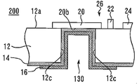
도 11 및 도 12는, 실시형태에 대한 비교예에 관한 반도체장치(200)를 나타낸 단면도다. 도 11은, 비교예에 관한 반도체장치(200)의 단면도이고, 실시형태에 관한 반도체장치(100)와의 차이는, Au층 18, 19를 구비하지 않고 있는 것이다. 도 12는, 반도체장치(200)가 형성된 반도체 기판(12)을 땜납으로 다이본드한 경우에, Ni층(16)과 땜납의 밀착성이 나쁘므로 땜납층(32) 내부에 있어서의 Ni층(16) 주변에 보이드(132)가 발생한 상태를 나타내고 있다.11 and 12 are cross-sectional views showing a
트랜지스터의 소스 접지를 행하기 위한 전기적 접속방법으로서, 소스 전극에 와이어를 거는 방법과, 소스 전극에 접속하도록 비아홀을 형성하는 방법이 있다. 소스 전극에 비아홀(30)을 형성하는 경우, 일반적으로, 비아홀(30)의 내면에 설치하는 금속으로서 Au가 사용되고 있다.As an electrical connection method for performing source grounding of a transistor, there are a method of attaching a wire to a source electrode and a method of forming a via hole to be connected to a source electrode. In the case of forming the via
땜납과 Au층(비아홀(30) 내부 및 소스 전극 부분)이 접하면, AuSn 반응을 일으킨다. 다이본드시에, 비아홀(30) 내부에 있어서 Au층 14가 땜납과 접하고 있으면, AuSn 반응이 일어난다. 이 AuSn 반응에 의해 땜납이 소스 전극표면까지 기어오른다고 하는 문제가 있다. 이 땜납의 기어오름은, 트랜지스터 영역까지 AuSn 반응을 확산시키게 되어, 트랜지스터(26)가 정상적으로 동작하지 않게 된다.When the solder and the Au layer (inside the via
비교예에 관한 반도체장치(200)는, 이 기어오름의 대책으로서, 비아홀(30) 내부에 땜납과의 반응을 배리어할 수 있는 Ni층(16)을 형성하고 있다. Ni층(16)에 의해, 땜납의 기어오름을 방지하는 것이 가능해진다.The
그렇지만, 한편으로, Ni층(16)은 땜납과의 밀착성이 나쁘므로, 땜납 내부에 공기가 남는 영역이 발생해 버린다고 하는 문제가 있다. 땜납 내부에 공기가 남는 이 영역은, 보이드라고도 불린다. 보이드(132)는 트랜지스터(26)의 동작시에 발생하는 열의 확산을 방해하게 되어, 결과적으로, 트랜지스터(26)의 특성을 저하시켜 버린다. 또한, 보이드(132)가 있음으로써 땜납과 반도체 기판(12)측의 밀착성이 낮아져, 벗겨짐을 유발해 버리는 것도 생각된다.On the other hand, on the other hand, since the
이 점에서, 실시형태에 관한 반도체장치(100)에 따르면, 비아홀(30) 내부에 있어서 Ni층(16)의 표면(12a)측 부분에 Au층 19를 부분적으로 설치하고 있다. Ni층(16)으로 Au층 14와 땜납 사이의 반응을 방지하면서, 비아홀(30) 내부의 Au층 19로 땜납의 밀착성을 높였으므로 비아홀(30) 내부에서 보이드가 생기는 것을 억제할 수 있다.In this regard, according to the
이때, 실시형태에 있어서는, Au층 19는, 개구(12d)의 저면을 구성하는 소스 전극(20)의 밑면(20b)의 윗쪽(즉, 비아홀(30)의 저면의 위쪽)에만 부분적으로 설치되어 있다. 이때, 여기에서 말하는 「밑면(20b)의 윗쪽」은, 도 1의 지면 윗쪽을 의미하는 것이 아니고, 밑면(20b)의 법선 방향을 의미한다. 한편, 비아홀(30)의 측면(즉, 개구(12d)의 측면(12c))에 있어서는, Au층 19가 설치되어 있지 않으므로, Ni층(16)이 노출되어 있다. 그렇지만, 본 발명은 이것에 한정되는 것은 아니다. 비아홀(30) 내부의 적어도 일부에 Au층을 설치하면 되고, 그 위치는 반드시 개구(12d)의 저면측에 한정되지 않는다.At this time, in the embodiment, the
도 6은, 본 발명의 실시형태의 변형예에 관한 반도체장치(111)를 나타낸 단면도다. 반도체장치 111은, 비아홀(40)을 구비하고 있는 점을 제외하고, 반도체장치 100과 같다. 비아홀(40)은, 개구(12d) 내부에 있어서 Ni층(16)의 전부를 덮도록 설치된 Au층 38을 구비하고 있다. Au층 38은, 개구(12d)의 저면을 구성하는 소스 전극(20)의 밑면(20b)의 윗쪽(즉, 비아홀(40)의 저면의 위쪽)과, 비아홀(40)의 측면(즉, 개구(12d)의 측면(12c))의 양쪽 모두를 덮는다. 이와 같이 함으로써, Ni층(16)과 땜납층(32)이 접하는 부분이 없어져, 비아홀(40) 내부에 구석구석까지 땜납을 충전시킬 수 있어, 보이드를 억제할 수 있다.6 is a cross-sectional view showing a
이때, 배리어 메탈층으로서 Ni층(16)을 설치했지만, 본 발명은 이것에 한정되지 않는다. Ni층(16) 대신에, Ni층(16)과 동일한 위치에, 백금(Pt), 납(Pb), 티타늄(Ti), 및 Cobalt(Co)로 이루어진 군으로부터 선택한 1개의 재료로 형성한 배리어 메탈층을 설치해도 된다. 이들 재료는, 니켈과 마찬가지로 땜납과의 반응성이 낮기 때문이다.At this time, the
도 7은, 본 발명의 실시형태의 변형예에 관한 반도체장치(112)를 나타낸 단면도다. 반도체장치 112는, Ni층(16)을 산화 Ni층(42)으로 치환한 점을 제외하고, 반도체장치 100과 같다. 즉, 반도체장치 112에 있어서, Au층 19는, 산화 Ni층(42) 중 저면에 중첩된 부분을 덮고, 산화 Ni층(42) 중 측면에 중첩된 부분을 덮지 않는다. 그 결과, 산화 Ni층(42)은 노출부(42a)를 갖는다. 이 노출부(42a)는, 반도체장치 112에 있어서의 비아홀(30)의 측면을 구성하고 있다.7 is a cross-sectional view showing a
일반적으로 Au층과 비교해서 Ni층 쪽이 메탈의 응력이 높다. 장벽을 높이기 위해서 Ni층(16)을 두껍게 하면, 반도체 기판(12)으로부터 Ni층(16)이 벗겨지기 쉬워져 버린다. 이 벗겨짐을 억제하고자 하여 단순히 Ni층(16)을 얇게 하면, 배리어 메탈층으로서의 효과가 불충분해진다. Ni층(16)과 땜납도 Au층보다 매우 느리기는 하지만 반응이 일어나므로, 단순하게 Ni층(16)을 얇게 할 수는 없다.Generally, the stress of the metal is higher in the Ni layer than in the Au layer. If the thickness of the
니켈보다도, 산화 니켈 쪽이 땜납을 강하게 밀어내는 성질을 갖고 있다. 이 때문에, 산화 Ni층(42) 쪽이, Ni층(16)보다도 막두께를 얇게 하는 것이 가능해진다.Nickel oxide has a property of pushing the solder more strongly than nickel. Therefore, the thickness of the Ni layer (42) can be made thinner than that of the Ni layer (16).
따라서, 반도체장치 112에서는, 배리어성(barrier property)이 보다 높은 산화 니켈로 형성한 산화 Ni층(42)을, 배리어 메탈층으로서 사용하고 있다. 산화 Ni층(42)은 Ni층(16)보다 땜납을 강하게 밀어낼 수 있기 때문에, 배리어 메탈층의 막두께를 얇게 해도 Au층 14를 땜납으로부터 배리어하는 효과를 충분히 얻을 수 있다. 이에 따라, 배리어 메탈로서의 확보를 하면서 산화 Ni층(42)을 얇게 하여, 벗겨짐의 문제를 억제할 수 잇다.Therefore, in the
반도체장치 112의 제조 프로세스로서는, 실시형태 1에 관한 Ni층(16)과 마찬가지로 Ni층을 형성한 후, 그 Ni층을 산화시켜, 산화 니켈(NiOx)로 한다. 그 후에, 실시형태 1과 마찬가지로 Au층 18, 19를 적층한다.As a manufacturing process of the
이때, 산화 Ni층(42) 대신에, 백금(Pt), 납(Pb), 티타늄(Ti),및 Cobalt(Co)로 이루어진 군으로부터 선택한 1개의 재료의 산화물층을 설치해도 된다.At this time, an oxide layer of one material selected from the group consisting of platinum (Pt), lead (Pb), titanium (Ti), and cobalt (Co) may be provided instead of the
도 8은, 본 발명의 실시형태의 변형예에 관한 반도체장치(113)를 나타낸 단면도다. 반도체장치 113은, 도 6에 나타낸 반도체장치(111)에 있어서, Ni층(16)을 산화 Ni층(42)으로 치환한 것이다.8 is a cross-sectional view showing a
도 9는, 본 발명의 실시형태의 변형예에 관한 반도체장치(114)를 나타낸 단면도다. 반도체장치 114는, Ni층(16)을 배리어 메탈층(50)으로 치환한 점을 제외하고, 반도체장치 100과 같다. 배리어 메탈층(50)은, Ni층과, 니켈 이외의 후술하는 재료로 이루어진 중간층을 적어도 1회 이상 서로 중첩하여 적층한 다층막 구조를 갖고 있다. 배리어 메탈층(50)에 있어서 Ni층은 중간층보다도 두껍게 되어 있다.9 is a sectional view showing a
배리어 메탈층(50)에 있어서는, Ni층/중간층/Ni층/중간층/…으로 복수회 서로 중첩하여 적층하여, Ni층과 중간층의 다층 구조로 한다. 중간층의 재료는, 니켈보다도 층 내부의 응력이 낮은 재료로서, 구체적으로는 티타늄(Ti), 금(Au), 백금(Pt), 알루미늄(Al), 니오브(Nb), 납(Pb) 및 구리(Cu)로 이루어진 군으로부터 선택한 1개의 재료를 사용해도 된다.In the
다층 구조로 함으로써, Ni층의 한 개 한개를 얇게 하고, 또한, Ni층 사이에 니켈보다 응력이 낮은 메탈로 이루어진 중간층을 삽입하도록 한다. 이에 따라, 배리어 메탈층(50)과 실시형태 1의 Ni층(16) 사이에서 Ni층으로서 본 경우의 최종적인 총 두께는 동일해도, 배리어 메탈층(50) 쪽이 Ni층(16)보다도 내부의 응력을 저감시킬 수 있다.By adopting a multilayer structure, one of the Ni layers is thinned, and an intermediate layer made of a metal having lower stress than nickel is inserted between the Ni layers. The total thickness of the
예를 들면, 반도체장치(100)에 있어서 Ni층(16)을 단층으로 100nm으로 하고 있었을 경우를 상정한다. 이에 대하여, 반도체장치 114에 있어서는, Ni층/중간층/Ni층/중간층/Ni층/중간층/Ni층/중간층/Ni층이라고 하는 것 같이 Ni층이 5층과 중간층이 4층으로 하고, Ni층을 1층당 20nm로 하고, 중간층은 1층당 10nm로 한다. 배리어 메탈층(50)은 Ni층이 1층당 20nm이기는 하지만, 합계 5층이 있기 때문에 총 두께로서는 Ni층(16)과 동일한 100nm의 두께의 Ni층을 갖는다. 이와 같이, Ni층의 두께를 충분히 확보해서 땜납에 대한 배리어성을 동일하게 하면서, 내부의 응력을 저감하는 것이 바람직하다.For example, it is assumed that the
이때, 반도체장치 114에 있어서도, Au층 19는, 배리어 메탈층(50) 중 개구(12d)의 저면에 중첩된 부분을 덮고, 배리어 메탈층(50) 중 측면(12c)에 중첩된 부분을 덮지 않는다. 그 결과, 배리어 메탈층(50)은 노출부(50a)를 갖는다. 이 노출부(50a)는, 비아홀(30)의 측면을 구성하고 있다.At this time, also in the
도 10은, 본 발명의 실시형태의 변형예에 관한 반도체장치(115)를 나타낸 단면도다. 반도체장치 115는, Ni층(16)을 배리어 메탈층(50)으로 치환한 점을 제외하고, 반도체장치(111)와 동일하다.10 is a cross-sectional view showing a
이하, 도 6∼도 10에서는 설명의 편의상, 땜납층(32)은 도시를 생략하고 잇지만, 실제로는 반도체장치 111∼115도 반도체 장치 100과 마찬가지로 땜납층(32)을 갖고 있다.
Hereinafter, in FIGS. 6 to 10, the
12 반도체 기판, 12a 표면, 12b 이면, 12c 측면, 12d 개구, 14, 18, 19, 38 Au층, 16 Ni층, 16a 노출부, 20 소스 전극, 20a 윗면, 20b 밑면, 22 게이트 전극, 24 드레인 전극, 26 트랜지스터, 30, 40 비아홀, 32 땜납층, 42 산화 Ni층, 42a 노출부, 50 배리어 메탈층, 50a 노출부, 100, 111, 112, 113, 114, 115 반도체장치, 132 보이드12 source electrode, 20a upper surface, 20b bottom surface, 22 gate electrode, 24 drain electrode, 12D semiconductor substrate, 12a surface, 12b side surface, 12c side surface, 12d opening, 14, 18, 19, 38Au layer, 16Ni layer, Electrode, 26 transistor, 30, 40 via hole, 32 solder layer, 42 Ni oxide layer, 42a exposed portion, 50 barrier metal layer, 50a exposed portion, 100, 111, 112, 113, 114, 115 semiconductor device, 132 void
Claims (12)
상기 개구의 측면 및 저면을 덮는 제1금속층과,
상기 개구 내부에 있어서 상기 제1금속층을 덮도록 설치된 배리어 메탈층과,
상기 배리어 메탈층의 재료보다도 땜납에 대한 밀착성이 높은 재료로 형성되고, 상기 개구 내부에 있어서 상기 배리어 메탈층의 적어도 일부를 덮도록 상기 배리어 메탈층에 적층된 제2금속층을 구비하고,
상기 제2금속층은, 상기 배리어 메탈층 중 상기 저면에 중첩된 부분을 덮고, 상기 배리어 메탈층 중 상기 측면에 중첩된 부분의 적어도 일부를 노출시키는 것을 특징으로 하는 반도체장치.
A semiconductor substrate provided with a front surface and a back surface and provided with a semiconductor element and an electrode of the semiconductor element on the surface and an opening reaching the bottom surface of the electrode,
A first metal layer covering the side surface and the bottom surface of the opening,
A barrier metal layer provided so as to cover the first metal layer in the opening,
And a second metal layer formed on the barrier metal layer so as to cover at least a part of the barrier metal layer in the opening, the barrier metal layer being made of a material having higher solder adhesion than the material of the barrier metal layer,
Wherein the second metal layer covers at least a portion of the barrier metal layer that overlaps the bottom surface and exposes at least a portion of the barrier metal layer that overlaps the side surface.
상기 배리어 메탈층은, 니켈, 백금, 납, 티타늄, 및 코발트로 이루어진 군으로부터 선택한 1개의 재료로 형성된 것을 특징으로 하는 반도체장치.
The method according to claim 1,
Wherein the barrier metal layer is formed of one material selected from the group consisting of nickel, platinum, lead, titanium, and cobalt.
상기 배리어 메탈층은, 니켈, 백금, 납, 티타늄, 및 코발트로 이루어진 군으로부터 선택한 1개의 재료의 산화물로 형성된 것을 특징으로 하는 반도체장치.
The method according to claim 1,
Wherein the barrier metal layer is formed of an oxide of one material selected from the group consisting of nickel, platinum, lead, titanium, and cobalt.
상기 배리어 메탈층은,
제1배리어 메탈층과,
상기 제1배리어 메탈층의 재료보다도, 층 내부의 응력이 낮은 재료로 이루어진 제2배리어 메탈층을
적어도 1회 이상 서로 중첩하여 적층한 것인 것을 특징으로 하는 반도체장치.
The method according to claim 1,
Wherein the barrier metal layer
A first barrier metal layer,
A second barrier metal layer made of a material having a lower stress in the layer than the material of the first barrier metal layer
And at least one layer is stacked on top of each other.
상기 제1배리어 메탈층이 니켈로 형성되고,
상기 제2배리어 메탈층이, 백금, 납, 티타늄, 금, 알루미늄, 니오브, 및 구리로 이루어진 군으로부터 선택한 1개의 재료로 형성된 것을 특징으로 하는 반도체장치.
8. The method of claim 7,
Wherein the first barrier metal layer is formed of nickel,
Wherein the second barrier metal layer is formed of one material selected from the group consisting of platinum, lead, titanium, gold, aluminum, niobium, and copper.
상기 제1배리어 메탈층은, 상기 제2배리어 메탈층보다도 두꺼운 것을 특징으로 하는 반도체장치.
8. The method of claim 7,
Wherein the first barrier metal layer is thicker than the second barrier metal layer.
상기 배리어 메탈층은, 상기 개구의 내부로부터 상기 이면에 있어서의 상기 개구의 가장자리부까지 설치되고 상기 가장자리부의 외측에는 설치되어 있지 않은 것을 특징으로 하는 반도체장치.
The method according to claim 1,
Wherein the barrier metal layer is provided from the inside of the opening to the edge portion of the opening in the back surface and is not provided outside the edge portion.
상기 반도체 소자가 트랜지스터이고, 상기 표면에 게이트, 소스, 드레인이 이 순서로 나란하게 설치되고,
상기 전극이 상기 소스 위에 설치한 소스 전극인 것을 특징으로 하는 반도체장치.
The method according to claim 1,
Wherein the semiconductor element is a transistor, and a gate, a source, and a drain are provided in parallel on the surface in this order,
And the electrode is a source electrode provided on the source.
상기 제1금속층 및 상기 제2금속층이 금을 포함하고, 상기 배리어 메탈층이 니켈을 포함하는 것을 특징으로 하는 반도체장치.The method according to claim 1,
Wherein the first metal layer and the second metal layer include gold, and the barrier metal layer includes nickel.
Applications Claiming Priority (2)
| Application Number | Priority Date | Filing Date | Title |
|---|---|---|---|
| JPJP-P-2013-247862 | 2013-11-29 | ||
| JP2013247862A JP6277693B2 (en) | 2013-11-29 | 2013-11-29 | Semiconductor device |
Publications (2)
| Publication Number | Publication Date |
|---|---|
| KR20150062963A KR20150062963A (en) | 2015-06-08 |
| KR101596232B1 true KR101596232B1 (en) | 2016-02-22 |
Family
ID=53058633
Family Applications (1)
| Application Number | Title | Priority Date | Filing Date |
|---|---|---|---|
| KR1020140164164A KR101596232B1 (en) | 2013-11-29 | 2014-11-24 | Semiconductor device |
Country Status (5)
| Country | Link |
|---|---|
| US (1) | US9355937B2 (en) |
| JP (1) | JP6277693B2 (en) |
| KR (1) | KR101596232B1 (en) |
| CN (1) | CN104681541B (en) |
| DE (1) | DE102014221620B4 (en) |
Families Citing this family (8)
| Publication number | Priority date | Publication date | Assignee | Title |
|---|---|---|---|---|
| CN107980171B (en) * | 2016-12-23 | 2022-06-24 | 苏州能讯高能半导体有限公司 | Semiconductor chip, semiconductor wafer, and method for manufacturing semiconductor wafer |
| JP6863574B2 (en) * | 2017-02-22 | 2021-04-21 | 住友電工デバイス・イノベーション株式会社 | Manufacturing method of semiconductor devices |
| JP2019145546A (en) * | 2018-02-16 | 2019-08-29 | 住友電工デバイス・イノベーション株式会社 | Manufacturing method of semiconductor device |
| US10967463B2 (en) * | 2018-04-11 | 2021-04-06 | The University Of Toledo | Sn whisker growth mitigation using NiO sublayers |
| WO2020137830A1 (en) * | 2018-12-27 | 2020-07-02 | 株式会社大真空 | Piezoelectric vibration device |
| CN109920757B (en) * | 2019-01-31 | 2020-08-25 | 厦门市三安集成电路有限公司 | Back section process for improving reliability of compound semiconductor device |
| US10861792B2 (en) * | 2019-03-25 | 2020-12-08 | Raytheon Company | Patterned wafer solder diffusion barrier |
| CN113809030B (en) * | 2021-11-16 | 2022-03-15 | 深圳市时代速信科技有限公司 | Semiconductor device and method for manufacturing semiconductor device |
Citations (2)
| Publication number | Priority date | Publication date | Assignee | Title |
|---|---|---|---|---|
| JP2003045877A (en) * | 2001-08-01 | 2003-02-14 | Sharp Corp | Semiconductor device and its manufacturing method |
| JP2007095853A (en) * | 2005-09-27 | 2007-04-12 | Matsushita Electric Ind Co Ltd | Semiconductor device and manufacturing method thereof |
Family Cites Families (20)
| Publication number | Priority date | Publication date | Assignee | Title |
|---|---|---|---|---|
| JPS63127550A (en) * | 1986-11-17 | 1988-05-31 | Nec Corp | Manufacture of semiconductor device |
| US4827610A (en) * | 1987-08-31 | 1989-05-09 | Texas Instruments Incorporated | Method of creating solder or brazing barriers |
| US5156998A (en) | 1991-09-30 | 1992-10-20 | Hughes Aircraft Company | Bonding of integrated circuit chip to carrier using gold/tin eutectic alloy and refractory metal barrier layer to block migration of tin through via holes |
| JP3350152B2 (en) | 1993-06-24 | 2002-11-25 | 三菱電機株式会社 | Semiconductor device and method of manufacturing the same |
| JPH0766384A (en) | 1993-08-23 | 1995-03-10 | Matsushita Electric Ind Co Ltd | Manufacture of semiconductor device |
| JPH07193214A (en) * | 1993-12-27 | 1995-07-28 | Mitsubishi Electric Corp | Via-hole and its formation |
| JP3724110B2 (en) | 1997-04-24 | 2005-12-07 | 三菱電機株式会社 | Manufacturing method of semiconductor device |
| US6541301B1 (en) * | 1999-02-12 | 2003-04-01 | Brook David Raymond | Low RF loss direct die attach process and apparatus |
| US6764810B2 (en) * | 2002-04-25 | 2004-07-20 | Taiwan Semiconductor Manufacturing Co., Ltd | Method for dual-damascene formation using a via plug |
| US20030203210A1 (en) * | 2002-04-30 | 2003-10-30 | Vitex Systems, Inc. | Barrier coatings and methods of making same |
| JP5162909B2 (en) * | 2006-04-03 | 2013-03-13 | 豊田合成株式会社 | Semiconductor light emitting device |
| JP5553504B2 (en) | 2008-12-26 | 2014-07-16 | キヤノン株式会社 | Semiconductor device manufacturing method and semiconductor device |
| DE102009044086A1 (en) | 2009-09-23 | 2011-03-24 | United Monolithic Semiconductors Gmbh | Method for producing an electronic component and electronic component produced by this method |
| CN102237339B (en) * | 2010-04-28 | 2013-07-03 | 中国科学院微电子研究所 | Metal electroplating layer structure on back of chip and preparation method thereof |
| KR101781620B1 (en) * | 2010-09-01 | 2017-09-25 | 삼성전자주식회사 | method for manufacturing MOS transistor |
| TWI497602B (en) * | 2011-02-15 | 2015-08-21 | Tzu Hsiung Chen | Trench schottky diode and manufacturing mehtod thereof |
| US20120273948A1 (en) * | 2011-04-27 | 2012-11-01 | Nanya Technology Corporation | Integrated circuit structure including a copper-aluminum interconnect and method for fabricating the same |
| JP2013128062A (en) * | 2011-12-19 | 2013-06-27 | Elpida Memory Inc | Semiconductor device manufacturing method |
| US8754531B2 (en) * | 2012-03-14 | 2014-06-17 | Nanya Technology Corp. | Through-silicon via with a non-continuous dielectric layer |
| JP6002447B2 (en) | 2012-05-30 | 2016-10-05 | 株式会社Fujiya | Resin foam board |
-
2013
- 2013-11-29 JP JP2013247862A patent/JP6277693B2/en active Active
-
2014
- 2014-08-22 US US14/465,884 patent/US9355937B2/en active Active
- 2014-10-24 DE DE102014221620.6A patent/DE102014221620B4/en active Active
- 2014-11-24 KR KR1020140164164A patent/KR101596232B1/en active IP Right Grant
- 2014-11-28 CN CN201410709725.8A patent/CN104681541B/en active Active
Patent Citations (2)
| Publication number | Priority date | Publication date | Assignee | Title |
|---|---|---|---|---|
| JP2003045877A (en) * | 2001-08-01 | 2003-02-14 | Sharp Corp | Semiconductor device and its manufacturing method |
| JP2007095853A (en) * | 2005-09-27 | 2007-04-12 | Matsushita Electric Ind Co Ltd | Semiconductor device and manufacturing method thereof |
Also Published As
| Publication number | Publication date |
|---|---|
| CN104681541A (en) | 2015-06-03 |
| US20150155224A1 (en) | 2015-06-04 |
| KR20150062963A (en) | 2015-06-08 |
| CN104681541B (en) | 2018-06-29 |
| US9355937B2 (en) | 2016-05-31 |
| JP6277693B2 (en) | 2018-02-14 |
| DE102014221620A1 (en) | 2015-06-03 |
| JP2015106638A (en) | 2015-06-08 |
| DE102014221620B4 (en) | 2018-08-02 |
Similar Documents
| Publication | Publication Date | Title |
|---|---|---|
| KR101596232B1 (en) | Semiconductor device | |
| US8227341B2 (en) | Semiconductor device and method of manufacturing the same | |
| US9136232B2 (en) | Method for bonding wafers and structure of bonding part | |
| US7795115B2 (en) | Method of manufacturing semiconductor device | |
| TWI627721B (en) | Method of manufacturing semiconductor device | |
| JP2001351920A (en) | Semiconductor device and its manufacturing method | |
| JPS63283040A (en) | Semiconductor device | |
| US20070235882A1 (en) | Semiconductor device and method for fabricating the same | |
| US10319634B2 (en) | Semiconductor device having MIM capacitor | |
| US20100013008A1 (en) | Semiconductor device and method of manufacturing the same | |
| US20080157098A1 (en) | Semiconductor device and method of manufacturing the same | |
| JP2015106638A5 (en) | ||
| JP5537625B2 (en) | Semiconductor light emitting device and manufacturing method thereof | |
| JP2023054250A (en) | Semiconductor device | |
| JP2022059085A (en) | Semiconductor device | |
| EP2996155B1 (en) | Semiconductor device and method for manufacturing a semiconductor device | |
| JP6634117B2 (en) | Semiconductor device | |
| JP6210482B2 (en) | Semiconductor device and manufacturing method of semiconductor device | |
| JP2008091457A (en) | Semiconductor device and manufacturing method therefor | |
| JP7382354B2 (en) | Semiconductor device and method for manufacturing semiconductor device | |
| JP2011238951A (en) | Semiconductor device and method of manufacturing same | |
| CN110690119A (en) | Semiconductor device and method for manufacturing semiconductor device | |
| JP2016219749A (en) | Semiconductor device and method of manufacturing the same | |
| TWI587418B (en) | Semiconductor device and method of manufacturing same | |
| JP6427838B2 (en) | Semiconductor device |
Legal Events
| Date | Code | Title | Description |
|---|---|---|---|
| A201 | Request for examination | ||
| E902 | Notification of reason for refusal | ||
| E701 | Decision to grant or registration of patent right | ||
| GRNT | Written decision to grant | ||
| FPAY | Annual fee payment |
Payment date: 20190201 Year of fee payment: 4 |
|
| FPAY | Annual fee payment |
Payment date: 20200205 Year of fee payment: 5 |