KR101589902B1 - Self-luminous display device and driving method of the same - Google Patents
Self-luminous display device and driving method of the same Download PDFInfo
- Publication number
- KR101589902B1 KR101589902B1 KR1020080127018A KR20080127018A KR101589902B1 KR 101589902 B1 KR101589902 B1 KR 101589902B1 KR 1020080127018 A KR1020080127018 A KR 1020080127018A KR 20080127018 A KR20080127018 A KR 20080127018A KR 101589902 B1 KR101589902 B1 KR 101589902B1
- Authority
- KR
- South Korea
- Prior art keywords
- light emitting
- emitting diode
- correction
- driving
- threshold voltage
- Prior art date
Links
Images


Classifications
-
- G—PHYSICS
- G09—EDUCATION; CRYPTOGRAPHY; DISPLAY; ADVERTISING; SEALS
- G09G—ARRANGEMENTS OR CIRCUITS FOR CONTROL OF INDICATING DEVICES USING STATIC MEANS TO PRESENT VARIABLE INFORMATION
- G09G3/00—Control arrangements or circuits, of interest only in connection with visual indicators other than cathode-ray tubes
- G09G3/20—Control arrangements or circuits, of interest only in connection with visual indicators other than cathode-ray tubes for presentation of an assembly of a number of characters, e.g. a page, by composing the assembly by combination of individual elements arranged in a matrix no fixed position being assigned to or needed to be assigned to the individual characters or partial characters
- G09G3/22—Control arrangements or circuits, of interest only in connection with visual indicators other than cathode-ray tubes for presentation of an assembly of a number of characters, e.g. a page, by composing the assembly by combination of individual elements arranged in a matrix no fixed position being assigned to or needed to be assigned to the individual characters or partial characters using controlled light sources
- G09G3/30—Control arrangements or circuits, of interest only in connection with visual indicators other than cathode-ray tubes for presentation of an assembly of a number of characters, e.g. a page, by composing the assembly by combination of individual elements arranged in a matrix no fixed position being assigned to or needed to be assigned to the individual characters or partial characters using controlled light sources using electroluminescent panels
- G09G3/32—Control arrangements or circuits, of interest only in connection with visual indicators other than cathode-ray tubes for presentation of an assembly of a number of characters, e.g. a page, by composing the assembly by combination of individual elements arranged in a matrix no fixed position being assigned to or needed to be assigned to the individual characters or partial characters using controlled light sources using electroluminescent panels semiconductive, e.g. using light-emitting diodes [LED]
- G09G3/3208—Control arrangements or circuits, of interest only in connection with visual indicators other than cathode-ray tubes for presentation of an assembly of a number of characters, e.g. a page, by composing the assembly by combination of individual elements arranged in a matrix no fixed position being assigned to or needed to be assigned to the individual characters or partial characters using controlled light sources using electroluminescent panels semiconductive, e.g. using light-emitting diodes [LED] organic, e.g. using organic light-emitting diodes [OLED]
- G09G3/3225—Control arrangements or circuits, of interest only in connection with visual indicators other than cathode-ray tubes for presentation of an assembly of a number of characters, e.g. a page, by composing the assembly by combination of individual elements arranged in a matrix no fixed position being assigned to or needed to be assigned to the individual characters or partial characters using controlled light sources using electroluminescent panels semiconductive, e.g. using light-emitting diodes [LED] organic, e.g. using organic light-emitting diodes [OLED] using an active matrix
- G09G3/3233—Control arrangements or circuits, of interest only in connection with visual indicators other than cathode-ray tubes for presentation of an assembly of a number of characters, e.g. a page, by composing the assembly by combination of individual elements arranged in a matrix no fixed position being assigned to or needed to be assigned to the individual characters or partial characters using controlled light sources using electroluminescent panels semiconductive, e.g. using light-emitting diodes [LED] organic, e.g. using organic light-emitting diodes [OLED] using an active matrix with pixel circuitry controlling the current through the light-emitting element
-
- G—PHYSICS
- G09—EDUCATION; CRYPTOGRAPHY; DISPLAY; ADVERTISING; SEALS
- G09G—ARRANGEMENTS OR CIRCUITS FOR CONTROL OF INDICATING DEVICES USING STATIC MEANS TO PRESENT VARIABLE INFORMATION
- G09G3/00—Control arrangements or circuits, of interest only in connection with visual indicators other than cathode-ray tubes
- G09G3/20—Control arrangements or circuits, of interest only in connection with visual indicators other than cathode-ray tubes for presentation of an assembly of a number of characters, e.g. a page, by composing the assembly by combination of individual elements arranged in a matrix no fixed position being assigned to or needed to be assigned to the individual characters or partial characters
- G09G3/22—Control arrangements or circuits, of interest only in connection with visual indicators other than cathode-ray tubes for presentation of an assembly of a number of characters, e.g. a page, by composing the assembly by combination of individual elements arranged in a matrix no fixed position being assigned to or needed to be assigned to the individual characters or partial characters using controlled light sources
- G09G3/30—Control arrangements or circuits, of interest only in connection with visual indicators other than cathode-ray tubes for presentation of an assembly of a number of characters, e.g. a page, by composing the assembly by combination of individual elements arranged in a matrix no fixed position being assigned to or needed to be assigned to the individual characters or partial characters using controlled light sources using electroluminescent panels
- G09G3/32—Control arrangements or circuits, of interest only in connection with visual indicators other than cathode-ray tubes for presentation of an assembly of a number of characters, e.g. a page, by composing the assembly by combination of individual elements arranged in a matrix no fixed position being assigned to or needed to be assigned to the individual characters or partial characters using controlled light sources using electroluminescent panels semiconductive, e.g. using light-emitting diodes [LED]
- G09G3/3208—Control arrangements or circuits, of interest only in connection with visual indicators other than cathode-ray tubes for presentation of an assembly of a number of characters, e.g. a page, by composing the assembly by combination of individual elements arranged in a matrix no fixed position being assigned to or needed to be assigned to the individual characters or partial characters using controlled light sources using electroluminescent panels semiconductive, e.g. using light-emitting diodes [LED] organic, e.g. using organic light-emitting diodes [OLED]
- G09G3/3266—Details of drivers for scan electrodes
-
- G—PHYSICS
- G09—EDUCATION; CRYPTOGRAPHY; DISPLAY; ADVERTISING; SEALS
- G09G—ARRANGEMENTS OR CIRCUITS FOR CONTROL OF INDICATING DEVICES USING STATIC MEANS TO PRESENT VARIABLE INFORMATION
- G09G2300/00—Aspects of the constitution of display devices
- G09G2300/08—Active matrix structure, i.e. with use of active elements, inclusive of non-linear two terminal elements, in the pixels together with light emitting or modulating elements
- G09G2300/0809—Several active elements per pixel in active matrix panels
- G09G2300/0819—Several active elements per pixel in active matrix panels used for counteracting undesired variations, e.g. feedback or autozeroing
-
- G—PHYSICS
- G09—EDUCATION; CRYPTOGRAPHY; DISPLAY; ADVERTISING; SEALS
- G09G—ARRANGEMENTS OR CIRCUITS FOR CONTROL OF INDICATING DEVICES USING STATIC MEANS TO PRESENT VARIABLE INFORMATION
- G09G2300/00—Aspects of the constitution of display devices
- G09G2300/08—Active matrix structure, i.e. with use of active elements, inclusive of non-linear two terminal elements, in the pixels together with light emitting or modulating elements
- G09G2300/0809—Several active elements per pixel in active matrix panels
- G09G2300/0842—Several active elements per pixel in active matrix panels forming a memory circuit, e.g. a dynamic memory with one capacitor
- G09G2300/0861—Several active elements per pixel in active matrix panels forming a memory circuit, e.g. a dynamic memory with one capacitor with additional control of the display period without amending the charge stored in a pixel memory, e.g. by means of additional select electrodes
- G09G2300/0866—Several active elements per pixel in active matrix panels forming a memory circuit, e.g. a dynamic memory with one capacitor with additional control of the display period without amending the charge stored in a pixel memory, e.g. by means of additional select electrodes by means of changes in the pixel supply voltage
-
- G—PHYSICS
- G09—EDUCATION; CRYPTOGRAPHY; DISPLAY; ADVERTISING; SEALS
- G09G—ARRANGEMENTS OR CIRCUITS FOR CONTROL OF INDICATING DEVICES USING STATIC MEANS TO PRESENT VARIABLE INFORMATION
- G09G2310/00—Command of the display device
- G09G2310/02—Addressing, scanning or driving the display screen or processing steps related thereto
- G09G2310/0243—Details of the generation of driving signals
- G09G2310/0254—Control of polarity reversal in general, other than for liquid crystal displays
- G09G2310/0256—Control of polarity reversal in general, other than for liquid crystal displays with the purpose of reversing the voltage across a light emitting or modulating element within a pixel
-
- G—PHYSICS
- G09—EDUCATION; CRYPTOGRAPHY; DISPLAY; ADVERTISING; SEALS
- G09G—ARRANGEMENTS OR CIRCUITS FOR CONTROL OF INDICATING DEVICES USING STATIC MEANS TO PRESENT VARIABLE INFORMATION
- G09G2320/00—Control of display operating conditions
- G09G2320/04—Maintaining the quality of display appearance
- G09G2320/043—Preventing or counteracting the effects of ageing
- G09G2320/045—Compensation of drifts in the characteristics of light emitting or modulating elements
-
- G—PHYSICS
- G09—EDUCATION; CRYPTOGRAPHY; DISPLAY; ADVERTISING; SEALS
- G09G—ARRANGEMENTS OR CIRCUITS FOR CONTROL OF INDICATING DEVICES USING STATIC MEANS TO PRESENT VARIABLE INFORMATION
- G09G3/00—Control arrangements or circuits, of interest only in connection with visual indicators other than cathode-ray tubes
- G09G3/20—Control arrangements or circuits, of interest only in connection with visual indicators other than cathode-ray tubes for presentation of an assembly of a number of characters, e.g. a page, by composing the assembly by combination of individual elements arranged in a matrix no fixed position being assigned to or needed to be assigned to the individual characters or partial characters
- G09G3/22—Control arrangements or circuits, of interest only in connection with visual indicators other than cathode-ray tubes for presentation of an assembly of a number of characters, e.g. a page, by composing the assembly by combination of individual elements arranged in a matrix no fixed position being assigned to or needed to be assigned to the individual characters or partial characters using controlled light sources
- G09G3/30—Control arrangements or circuits, of interest only in connection with visual indicators other than cathode-ray tubes for presentation of an assembly of a number of characters, e.g. a page, by composing the assembly by combination of individual elements arranged in a matrix no fixed position being assigned to or needed to be assigned to the individual characters or partial characters using controlled light sources using electroluminescent panels
- G09G3/32—Control arrangements or circuits, of interest only in connection with visual indicators other than cathode-ray tubes for presentation of an assembly of a number of characters, e.g. a page, by composing the assembly by combination of individual elements arranged in a matrix no fixed position being assigned to or needed to be assigned to the individual characters or partial characters using controlled light sources using electroluminescent panels semiconductive, e.g. using light-emitting diodes [LED]
- G09G3/3208—Control arrangements or circuits, of interest only in connection with visual indicators other than cathode-ray tubes for presentation of an assembly of a number of characters, e.g. a page, by composing the assembly by combination of individual elements arranged in a matrix no fixed position being assigned to or needed to be assigned to the individual characters or partial characters using controlled light sources using electroluminescent panels semiconductive, e.g. using light-emitting diodes [LED] organic, e.g. using organic light-emitting diodes [OLED]
- G09G3/3275—Details of drivers for data electrodes
- G09G3/3291—Details of drivers for data electrodes in which the data driver supplies a variable data voltage for setting the current through, or the voltage across, the light-emitting elements
-
- H—ELECTRICITY
- H01—ELECTRIC ELEMENTS
- H01L—SEMICONDUCTOR DEVICES NOT COVERED BY CLASS H10
- H01L2221/00—Processes or apparatus adapted for the manufacture or treatment of semiconductor or solid state devices or of parts thereof covered by H01L21/00
- H01L2221/10—Applying interconnections to be used for carrying current between separate components within a device
- H01L2221/1068—Formation and after-treatment of conductors
- H01L2221/1073—Barrier, adhesion or liner layers
- H01L2221/1084—Layers specifically deposited to enhance or enable the nucleation of further layers, i.e. seed layers
- H01L2221/1089—Stacks of seed layers
Landscapes
- Engineering & Computer Science (AREA)
- Physics & Mathematics (AREA)
- Computer Hardware Design (AREA)
- General Physics & Mathematics (AREA)
- Theoretical Computer Science (AREA)
- Control Of El Displays (AREA)
- Control Of Indicators Other Than Cathode Ray Tubes (AREA)
- Electroluminescent Light Sources (AREA)
Abstract
화소회로와, 구동회로를 포함한 자발광형 표시장치가 제공되며, 각 화소회로는 발광 다이오드, 상기 발광 다이오드의 구동전류 경로에 접속되는 구동 트랜지스터 및 상기 구동 트랜지스터의 제어 노드에 결합하는 유지 커패시터를 포함하고, 상기 발광 다이오드를 발광 가능하게 하기 전에 상기 구동 트랜지스터에 대하여 적어도 임계값전압 보정의 본 동작과 이동도 보정을 행하는 기간에, 상기 구동회로는, 상기 발광 다이오드가 비발광인 상태에서 상기 구동 트랜지스터의 예비의 임계값전압 보정, 즉 더미 Vth 보정을 행하고, 다음에, 상기 발광 다이오드를 역 바이어스 상태로 하여 상기 유지 커패시터의 유지 전압을 초기화하는 보정준비를 일정 기간 행하고, 보정준비 후, 임계값전압 보정의 본 동작과 상기 이동도 보정을 행한다.
발광 다이오드, 구동 트랜지스터, 유지 커패시터, 화소회로, 이동도 보정
There is provided a self-luminous display device including a pixel circuit and a driving circuit, wherein each pixel circuit includes a light emitting diode, a driving transistor connected to a driving current path of the light emitting diode, and a holding capacitor coupled to a control node of the driving transistor In a period during which the main operation and the mobility correction of at least the threshold voltage correction are performed on the driving transistor before the light emitting diode is allowed to emit light, The dummy Vth correction is performed. Next, the light emitting diode is set in the reverse bias state to prepare for correction for initializing the holding voltage of the holding capacitor for a predetermined period, and after the preparation of the correction, the threshold voltage This correcting operation and the mobility correction are performed.
Light emitting diodes, driving transistors, holding capacitors, pixel circuits, mobility correction
Description
본 발명은 2007년 12월 21일, 일본 특허청에 출원된 일본 특허 JP 2007-329845에 관한 주제를 포함하고, 그 모든 내용은 여기에 참조에 의해 포함된다.The present invention includes the subject matter of Japanese Patent JP 2007-329845 filed on December 21, 2007, the Japanese Patent Office, the entire contents of which are incorporated herein by reference.
본 발명은 바이어스 전압이 인가되었을 때 자발광하는 발광 다이오드와, 그 구동전류를 제어하는 구동 트랜지스터와, 구동 트랜지스터의 제어 노드에 결합하는 유지 커패시터를, 화소회로 내에 갖는 자발광형 표시장치와, 그 구동방법에 관한 것이다.The present invention relates to a self-luminous display device having a light emitting diode that self-emits light when a bias voltage is applied, a driving transistor for controlling the driving current, and a holding capacitor for coupling to a control node of the driving transistor, Driving method.
자발광형 표시장치에 이용되는 전기광학소자로서, 유기 전기루미네선스(Organic Electro Luminescence) 소자가 알려져 있다. 이 소자는 일반적으로 OLED(Organic Light Emitting Diode)라고 칭하며, 발광 다이오드의 일종이다.As an electro-optical element used in a self-emission type display device, an organic electro luminescence element is known. This device is generally called an OLED (Organic Light Emitting Diode) and is a kind of light emitting diode.
OLED는 적층된 복수의 유기박막을 갖는다. 이들 박막은, 예를 들면 유기 정공 수송층이나 유기 발광층 등으로서 기능한다. OLED는 유기박막에 전계를 인가하면 발광하는 현상을 이용한 전기광학소자다. 따라서 OLED를 전기광학소자로서 사용 하는 표시장치는 각 화소에 구동 트랜지스터와 커패시터를 포함하는 화소회로를 갖는다. 구동 트랜지스터는 OLED를 흐르는 전류량을 제어한다. 커패시터는 구동 트랜지스터의 제어 전압을 유지한다.The OLED has a plurality of stacked organic thin films. These thin films function as, for example, an organic hole transporting layer or an organic light emitting layer. OLEDs are electro-optic devices that emit light when an electric field is applied to the organic thin film. Therefore, a display device using an OLED as an electro-optical element has a pixel circuit including a driving transistor and a capacitor in each pixel. The driving transistor controls the amount of current flowing through the OLED. The capacitor holds the control voltage of the driving transistor.
지금까지 다양한 화소회로가 제안되어 왔다. 제안된 회로의 종류 중 주요한 것으로는 4트랜지스터(4T)·1커패시터(1C)형, 4T·2C형, 5T·1C형, 3T·1C형 등이 알려져 있다.Various pixel circuits have been proposed so far. Among the types of the proposed circuit, four transistors (4T), one capacitor (1C) type, 4T and 2C type, 5T and 1C type, 3T and 1C type, and the like are known.
상기 모든 화소회로는 트랜지스터의 특성 변동에 기인하는 화질저하를 방지하도록 설계된다. 트랜지스터는 TFT(Thin Film Transistor)로 형성된다. 이들 회로는 데이터 전압이 일정하면 화소회로 내부에서 구동전류가 일정하도록 제어하고, 이것에 의해 화면 전체의 유니포미티(휘도의 균일성)를 향상시킨다. 특히 화소회로 내에서 OLED를 전원에 접속할 때, 입력하는 영상 신호의 데이터 전위에 따라 전류량을 제어하는 구동 트랜지스터의 특성 변동이, 직접적으로 OLED의 발광 휘도에 영향을 준다.All the above-described pixel circuits are designed so as to prevent deterioration of image quality caused by characteristic variations of transistors. The transistor is formed of a TFT (Thin Film Transistor). These circuits control the driving current to be constant within the pixel circuit when the data voltage is constant, thereby improving the uniformity (uniformity of brightness) of the entire screen. Particularly, when the OLED is connected to the power source in the pixel circuit, the characteristic variation of the driving transistor controlling the amount of current depending on the data potential of the input video signal directly affects the light emission luminance of the OLED.
구동 트랜지스터의 특성 변동으로 가장 큰 것은 임계값전압의 변동이다. 이 때문에, 구동 트랜지스터의 임계값전압 변동에 기인하는 영향이 구동전류로부터 캔슬되도록, 구동 트랜지스터의 게이트 소스간 전압을 보정할 필요가 있다. 이하, 이 보정을 「임계값전압 보정 또는 임계값 보정」이라고 한다.The greatest variation in the characteristics of the driving transistor is the fluctuation of the threshold voltage. Therefore, it is necessary to correct the gate-source voltage of the driving transistor so that the influence due to the threshold voltage variation of the driving transistor is canceled from the driving current. Hereinafter, this correction is referred to as "threshold voltage correction or threshold value correction".
또한, 임계값전압 보정을 행하는 것을 전제로, 구동능력성분(일반적으로는, 이동도라고 불리고 있다)의 영향이 캔슬되도록 상기 게이트 소스간 전압을 보정하면, 보다 향상된 유니포미티를 얻을 수 있다. 이 성분은 구동 트랜지스터의 전류구 동능력에서 임계값 변동 기인 성분 등을 감산하여 얻는다. 이하, 이 구동능력성분의 보정을 「이동도 보정」이라고 한다.Further, it is possible to obtain a more uniform uniformity by correcting the gate-source voltage so that the effect of the drivability component (generally referred to as mobility) is canceled, on the premise of performing the threshold voltage correction. This component is obtained by subtracting a component such as a threshold value fluctuation factor from the current driving capability of the driving transistor. Hereinafter, correction of the driving ability component is referred to as " mobility correction. &Quot;
구동 트랜지스터의 임계값전압이나 이동도의 보정에 대해서는, 예를 들면 일본국 공개특허공보 특개 2006-215213호(이하, 특허문헌 1이라고 한다)에 상세하게 설명되어 있다.The correction of the threshold voltage and the mobility of the driving transistor is described in detail in, for example, Japanese Patent Application Laid-Open No. 2006-215213 (hereinafter referred to as Patent Document 1).
상기 특허문헌 1에 기재되어 있는 바와 같이, 화소회로의 구성에 따라서는, 임계값전압이나 이동도의 보정시에 발광 다이오드(유기 EL소자)는 비발광으로 하기 위해, 역바이어스 해야 한다. 이 경우, 표시 화면이 전환될 때에, 때로는, 화면 전체의 밝기가 순간적으로 변화되는 현상이 일어난다. 이 현상은, 순간적으로 화면이 밝게 빛나는 경우가 특히 눈에 띄기 때문에, 이하, 「플래쉬 현상」이라고 칭한다.As described in
본 발명은, 이 화면 전체의 밝기가 순간적으로 변화되는(플래쉬) 현상을 방지 또는 억제할 수 있는 자발광형 표시장치와, 그 구동방법에 관한 것이다.The present invention relates to a self-emission type display device capable of preventing or suppressing a phenomenon in which brightness of an entire screen is instantaneously changed (flash), and a driving method thereof.
본 발명의 일 형태(제1 형태)에 관련된 자발광형 표시장치는, 화소회로와, 이 화소회로의 구동을 행하는 구동회로를 갖는다. 각 화소회로는 발광 다이오드, 상기 발광 다이오드의 구동전류 경로에 접속되는 구동 트랜지스터 및 상기 구동 트랜지스터의 제어 노드에 결합하는 유지 커패시터를 포함한다.A self-emission type display device according to a first aspect of the present invention includes a pixel circuit and a driver circuit for driving the pixel circuit. Each pixel circuit includes a light emitting diode, a driving transistor connected to a driving current path of the light emitting diode, and a holding capacitor coupled to a control node of the driving transistor.
상기 구동회로는, 상기 발광 다이오드를 발광 가능하게 하기 전에 상기 구동 트랜지스터에 대하여 임계값전압 보정과 이동도 보정을 행하는 기간에, 상기 발광 다이오드의 비발광 상태로부터 상기 구동 트랜지스터의 예비의 임계값전압 보정(더미 Vth 보정)을 행한다. 다음에, 상기 발광 다이오드를 역 바이어스 상태로 하여 상기 유지 커패시터의 유지 전압을 초기화하는 보정준비를 일정 기간 행한다. 구동회로는 보정준비 후, 임계값전압 보정의 본 동작과 상기 이동도 보정을 행한다.Wherein the driving circuit is configured to perform a threshold voltage correction and a mobility correction of the driving transistor from a non-emission state of the light emitting diode to a preliminary threshold voltage correction (Dummy Vth correction) is performed. Next, the light emitting diode is set in the reverse bias state, and preparation for correction for initializing the holding voltage of the holding capacitor is performed for a predetermined period. The drive circuit performs the main operation of the threshold voltage correction and the mobility correction after preparation for correction.
본 발명의 다른 형태(제2 형태)에 관련된 자발광형 표시장치는, 상기 제1 형태의 특징에 더하여, 다음의 특징이 있다.A self-emission type display device according to another embodiment (second embodiment) of the present invention has the following features in addition to the features of the first embodiment.
즉, 제2 형태의 자발광형 표시장치는, 화소 어레이를 갖는다. 화소 어레이에는 복수의 상기 화소회로가 행렬 모양으로 배치된다. 상기 복수의 화소회로는 각각, 상기 제어 노드에 대하여, 데이터 전위를 샘플링하여 입력하는 샘플링 트랜지스터를 포함한다. 상기 구동회로는, 상기 샘플링 트랜지스터를 오프시킨 상태에서, 상기 구동 트랜지스터의 상기 발광 다이오드가 접속된 측과 반대측의 노드의 전원전압 접속을 해제함으로써 상기 발광 다이오드를 역 바이어스 상태로 설정한다. 다음에 구동회로는 상기 더미(dummy) Vth 보정 후에 상기 보정준비를 행한다. 보정준비 후, 구동회로는 상기 임계값전압 보정의 본 동작과 상기 이동도의 보정을 행한다. 상기 보정준비에서는, 상기 전원전압 접속의 해제 기간을, 상기 화소 어레이 내의 화소 행마다 정해진 모든 화면표시기간 내에서 일정하게 한다.That is, the self-emission type display device of the second embodiment has a pixel array. A plurality of the pixel circuits are arranged in a matrix form in the pixel array. Each of the plurality of pixel circuits includes a sampling transistor for sampling and inputting a data potential to the control node. The driving circuit sets the light emitting diode in a reverse bias state by releasing a power supply voltage connection of a node on the opposite side of a side to which the light emitting diode is connected to the driving transistor in a state in which the sampling transistor is turned off. Next, the drive circuit performs the above correction preparation after the dummy Vth correction. After preparation for correction, the drive circuit performs the main operation of the threshold voltage correction and the correction of the mobility. In the correction preparation, the release period of the power supply voltage connection is made constant within all screen display periods set for each pixel row in the pixel array.
본 발명의 다른 형태(제3 형태)에 관련된 자발광형 표시장치는, 상기 제2형태의 특징에 더하여, 다음의 특징이 있다.A self-emission type display device according to another embodiment (third embodiment) of the present invention has the following features in addition to the features of the second embodiment.
즉, 제3 형태의 자발광형 표시장치에 있어서, 상기 구동회로는, 직전의 다른 상기 화면표시기간에 있어서의 발광 종료를, 상기 역 바이어스 상태의 설정을 시작함으로써 변경 가능하게 제어한다.That is, in the self-luminous display device of the third aspect, the drive circuit controls the end of light emission in the immediately preceding screen display period to be changeable by starting the setting of the reverse bias state.
본 발명의 다른 형태(제4 형태)에 관련된 자발광형 표시장치는, 상기 제1 형태의 특징에 더하여, 다음의 특징이 있다.A self-emission type display device according to another embodiment (fourth embodiment) of the present invention has the following features in addition to the features of the first embodiment.
즉, 제4 형태의 자발광형 표시장치의 상기 구동회로는, 상기 비발광 상태의 설정과, 상기 구동 트랜지스터의 임계값전압의 등가전압을 상기 유지 커패시터에 유지시키는 임계값전압 보정(상기 더미 Vth 보정)을 행한다. 상기 구동회로는 임계값전압 보정의 본 동작과, 이동도 보정을, 일정한 기간 내에 상기 발광 다이오드의 역 바이어스 상태에서 행한다. 이동도 보정에서는, 데이터 전위를 상기 제어 노드에 기록하여 상기 구동 트랜지스터의 구동 능력에 따라 상기 유지 커패시터의 유지 전압을 조정한다. 그 결과, 상기 데이터 전위에 따라, 상기 발광 다이오드를 발광 가능한 상태로 순 바이어스 한다.That is, the drive circuit of the self-emission type display device of the fourth aspect is characterized in that the drive circuit for setting the non-emission state and the threshold voltage correction for holding the equivalent voltage of the threshold voltage of the drive transistor to the storage capacitor Correction) is performed. The driving circuit performs the main operation of the threshold voltage correction and the mobility correction in a reverse bias state of the light emitting diode within a predetermined period. In the mobility correction, a data potential is written to the control node to adjust the holding voltage of the holding capacitor in accordance with the driving ability of the driving transistor. As a result, the light emitting diode is forward-biased in a state capable of emitting light according to the data potential.
본 발명의 다른 형태(제5∼제6 형태)에 관련된 자발광형 표시장치는, 특별히 상세히 기술하지 않는다. 단, 제5∼제6 형태에 따른 자발광형 표시장치는, 상기 제1∼제4 형태를, 구체적인 신호선이나 제어선의 레벨제어로 나타내는 것이다.The self-emission type display apparatuses according to other forms (fifth to sixth embodiments) of the present invention are not described in detail in detail. However, the self-luminous display devices according to the fifth to sixth embodiments show the first to fourth embodiments by the level control of concrete signal lines and control lines.
본 발명의 다른 형태(제7 형태)에 관련된 자발광형 표시장치의 구동방법은, 화소회로를 구비하는 자발광형 표시장치의 구동방법이다. 각 화소회로는 발광 다이오드, 상기 발광 다이오드의 구동전류 경로에 접속되는 구동 트랜지스터, 및 상기 구동 트랜지스터의 제어 노드에 결합하는 유지 커패시터를 포함한다. 상기 구동방법은, 상기 발광 다이오드의 비발광 상태를 설정하는 비발광 설정 스텝을 포함한다. 상기 구동방법은, 상기 구동 트랜지스터의 예비의 임계값전압 보정을 행하는 더미 Vth 보정 스텝을 더 포함한다. 상기 구동방법은, 상기 발광 다이오드를 역 바이어스 상태로 하여 상기 유지 커패시터의 유지 전압을 초기화하는 보정준비 스텝을 더 포함한다. 상기 구동방법은, 상기 구동 트랜지스터의 임계값전압 보정을 행하는 본 동작의 임계값전압 보정 스텝을 더 포함한다. 상기 구동방법은, 상기 화소 회로에 데이터 전압을 기록해서 상기 구동 트랜지스터의 이동도 보정을 행하는 이동도 보정 스텝을 더 포함한다. 상기 구동방법은, 상기 기록한 데이터 전압에 따라, 상기 발광 다이오드를 발광 가능한 상태로 순 바이어스 하는 발광 설정 스텝을 포함한다.A driving method of a self-luminous display device according to another aspect (seventh aspect) of the present invention is a driving method of a self-luminous display device including a pixel circuit. Each pixel circuit includes a light emitting diode, a driving transistor connected to a driving current path of the light emitting diode, and a holding capacitor coupled to a control node of the driving transistor. The driving method includes a non-emission setting step of setting a non-emission state of the light emitting diode. The driving method further includes a dummy Vth correction step of performing a preliminary threshold voltage correction of the driving transistor. The driving method further includes a correction preparation step of initializing the holding voltage of the holding capacitor by placing the light emitting diode in a reverse bias state. The driving method further includes a threshold voltage correcting step of the present operation for correcting a threshold voltage of the driving transistor. The driving method further includes a mobility correction step of performing a mobility correction of the driving transistor by recording a data voltage in the pixel circuit. The driving method includes a light emission setting step of forward-biasing the light emitting diode in a state capable of emitting light according to the recorded data voltage.
본 발명의 다른 형태(제8 형태)에 관련된 자발광형 표시장치의 구동방법은, 상기 제7 형태의 특징에 더하여, 다음의 특징이 있다.A driving method of a self-emission type display device according to another aspect (eighth aspect) of the present invention has the following features in addition to the features of the seventh aspect.
즉, 제8 형태의 자발광형 표시장치의 구동방법은, 상기 더미 Vth 보정 스텝, 상기 보정준비 스텝, 상기 본 동작의 임계값전압 보정 스텝, 상기 이동도 보정 스텝, 상기 발광 설정 스텝 및 상기 비발광 설정 스텝을, 이 순서로 실행한다. 상기 구동방법에서는 상기 스텝을 상기 화소회로가 행렬 모양으로 배치된 화소 어레이 내의 화소 행마다 정해진 행 표시 기간에 대응하여 실행한다.That is, the driving method of the self-luminous display of the eighth aspect is characterized in that the dummy Vth correction step, the correction preparation step, the threshold voltage correction step of the main operation, the mobility correction step, And the light emission setting step are executed in this order. In the driving method, the step is executed in correspondence with a row display period determined for each pixel row in the pixel array in which the pixel circuits are arranged in a matrix.
본 발명의 다른 형태(제9 형태)에 관련된 자발광형 표시장치의 구동방법은, 상기 제7 형태의 특징에 더하여, 다음의 특징이 있다.A driving method of a self-emission type display device according to another aspect (ninth aspect) of the present invention has the following features in addition to the features of the seventh aspect.
즉, 제9 형태의 자발광형 표시장치의 구동방법은, 상기 보정준비 스텝, 상기 본 동작의 임계값전압 보정 스텝, 상기 이동도 보정 스텝, 상기 발광 설정 스텝, 상기 더미 Vth 보정 스텝 및 상기 비발광 설정 스텝을, 이 순서로 실행한다. 상기 구동방법에서는 상기 화소회로가 행렬 모양으로 배치된 화소 어레이 내의 화소 행마다 정해진 행 표시 기간에 대응하여 실행한다.That is, the driving method of the self-luminous display device of the ninth aspect is characterized in that the correction preparation step, the threshold voltage correction step of the main operation, the mobility correction step, the light emission setting step, the dummy Vth correction step, And the light emission setting step are executed in this order. In the driving method, the pixel circuits are executed in correspondence with the row display period determined for each pixel row in the pixel array arranged in a matrix.
본 발명의 다른 형태(제10 형태)에 관련된 자발광형 표시장치의 구동방법은, 상기 제7 형태의 특징에 더하여, 다음의 특징이 있다.A driving method of a self-emission type display device according to another aspect (tenth aspect) of the present invention has the following features in addition to the features of the seventh aspect.
즉, 제10 형태의 자발광형 표시장치의 구동방법에 의한 상기 보정준비 스텝에서는, 상기 역 바이어스 상태의 설정 기간을, 모든 상기 화면표시 기간 내에서 일정하게 한다.That is, in the correction preparation step by the driving method of the self-luminous display device of the tenth form, the setting period of the reverse bias state is made constant within all the screen display periods.
그러나, 본 발명자 등은, 전술한 「플래쉬 현상」의 원인을 해석한 결과, 이 현상은, 발광 다이오드(유기 EL소자 등)의 역 바이어스 기간의 길고 짧음에 관련되어 있음을 알아냈다.However, the present inventors have analyzed the cause of the above-described " flash phenomenon " and found that this phenomenon is related to a long and short reverse bias period of a light emitting diode (organic EL element, etc.).
유기 EL소자의 역 바이어스에 대해서, 상기 특허문헌 1에는, 5T·1C형의 화소회로에 있어서, 유기발광 다이오드 OLED(유기 EL소자)를 역바이어스 한 상태에서 임계값전압 보정을 행하는 제어가 기재되어 있다(상기 특허문헌 1의 제1 및 제2 실시예 참조, 예를 들면 제1 실시예에 있어서의 단락 [0046] 등의 기재 참조). 특허문헌 1에서는, 하나의 화소에 대한 구동에만 착안한 설명을 하고 있기 때문에 기재되어 있지 않지만, 실제의 유기 EL디스플레이에 있어서는, 유기 EL소자의 역 바이어스는, 1필드 앞에 화면표시 기간(1F)에 있어서의 발광 종점부터 시작되어, 보정기간을 거쳐 다음의 발광시에 해소된다. 그 때문에 역 바이어스의 길이(시작점)가, 유기 EL소자의 발광 허가 기간의 길이에 의존하고, 때로는 변화된다.Regarding the reverse bias of the organic EL element, the above-described
유기 EL소자는, 흐르는 전류량이 극단적으로 커지면 경시 변화에 의해, 그 특성이 저하한다. 이 특성의 저하는, 전술한 임계값전압이나 이동도의 보정으로 어느 정도 보상(보정)된다. 그러나 극단적인 특성 저하는 완전히 보정할 수 없다. 따라서 특성 저하는 처음부터 작은 쪽이 바람직하다. 그 결과, 발광 휘도를 높이는 제어를 행할 경우, 구동 전류량을 높이는 것이 아닌 발광 허가 기간을 길게 하는 제어(펄스의 듀티비 제어)를 행하는 경우가 있다.In the organic EL device, when the amount of current flowing becomes extremely large, the characteristics of the organic EL device deteriorate due to changes over time. The degradation of this characteristic is compensated (corrected) to some extent by the correction of the above-described threshold voltage or mobility. However, extreme degradation can not be completely corrected. Therefore, the lowering of the characteristic is preferable from the beginning. As a result, in the case of performing control to increase the light emission luminance, control (duty ratio control of pulse) is performed to lengthen the light emission permission period, not to increase the amount of driving current.
또한 화면 주위의 환경이 밝을 때에는, 화면을 보기 쉽게 하기 위해, 상기 보정의 한계를 고려하여 발광 허가 기간을 길게 하는 제어를 행하는 경우가 있다. 또한, 저소비 전력화의 요구로 휘도를 낮출 때, 구동전류량을 낮추기보다는 발광 시간을 짧게 하는 경우가 있다.Further, when the environment around the screen is bright, in order to make the screen easy to see, there is a case where control is performed to lengthen the light emission permission period in consideration of the limit of the correction. Further, when lowering the luminance by reducing the power consumption, there is a case where the light emission time is shortened rather than the driving current amount is lowered.
화면의 밝기를, 평균적인 화소의 발광 휘도를 높고 낮게 하여 변화시킬 경우, 그 화면의 변환시에 「플래쉬 현상」이 관측된다. 따라서 역 바이어스 기간의 길고 짧음에 따라 플래쉬 현상이 각각 다르게 나타난다. 이 관점에서, 본 발명자 등은, 발광 다이오드(유기 EL소자 등)를 역 바이어스 할 때, 발광 다이오드의 등가 용량값이 시간적으로 변화되고, 이것이 보정의 정밀도에 영향을 주기 때문에, 휘도가 화면 전체에서 변화된다는 결론을 얻었다.When the brightness of the screen is changed by increasing and decreasing the light emission luminance of an average pixel, a " flash phenomenon " is observed at the time of conversion of the screen. Therefore, the flash phenomenon is different according to the length of the reverse bias period. From this point of view, the inventors of the present invention have found that when reversely biasing a light emitting diode (such as an organic EL element), the equivalent capacitance value of the light emitting diode changes with time and this affects the accuracy of correction, It was changed.
이 때, 발광 다이오드의 비발광 설정(발광하고 있는 경우에는 발광 정지)은, 전술한 바와 같이 역 바이어스 상태의 설정에 의해 행해지는 것이 일반적이다. 그러나 역 바이어스 상태로 하지 않더라도, 예를 들면 바이어스 0에서도 비발광 설정은 가능하다.At this time, it is general that the non-emission setting (light emission stop in the case of emitting light) of the light emitting diode is performed by setting the reverse bias state as described above. However, even if the reverse bias state is not set, for example, even in the
따라서, 본 발명의 전술한 제1∼제 10형태에서는, 발광 다이오드의 비발광 설정(발광하고 있는 경우에는 발광 정지, 예를 들면 역 바이어스 상태설정)의 동작과, 보정준비를 위해 행하는 역 바이어스 상태 설정 사이에, 발광 다이오드의 비발광 상태로부터 구동 트랜지스터의 예비의 임계값전압 보정(더미 Vth 보정)을 행한다. 이로써 더미 Vth 보정 후의 역 바이어스 설정 기간(일반적으로는 보정준비 기 간)을 일정하게 하고 있다. 더미 Vth 보정은, 그 후에 행하는 임계값전압 보정의 본 동작과 제어 자체는 비슷하며, 유지 커패시터에 임계값전압을 유지시키는 동작이다. 그러나, 더미 Vth 보정 후에 유지 커패시터의 유지 전압 초기화(보정준비)가 행해진다. 이에 따라 더미 Vth 보정으로 행한 임계값전압 보정은 무효가 된다(본 동작의 임계값전압 보정에 기여하지 않는다). 더미 Vth 보정은 초기화에서 행해지는 역 바이어스 설정의 시점을 결정하는 작용이 있다. 이에 따라 다시 초기화가 일정 기간 동안 행해진다.Therefore, in the above-described first to tenth embodiments of the present invention, the operation of the non-emission setting of the light-emitting diode (emission stop when light is emitted, for example, reverse bias state setting) Preliminary threshold voltage correction (dummy Vth correction) of the drive transistor is performed from the non-emission state of the light emitting diode. As a result, the reverse bias setting period after the dummy Vth correction (generally, the preparation period for calibration) is made constant. The dummy Vth correction is similar to the main operation of the threshold voltage correction to be performed thereafter and the operation itself to maintain the threshold voltage to the holding capacitor. However, after the dummy Vth correction, the holding voltage of the holding capacitor is initialized (preparation for calibration). Accordingly, the threshold voltage correction performed by the dummy Vth correction is invalidated (it does not contribute to the threshold voltage correction of this operation). The dummy Vth correction has an effect of determining the time point of reverse bias setting performed in initialization. Thus, reinitialization is performed for a certain period of time.
유지 전압의 초기화 기간, 즉 역 바이어스 설정 기간을 일정 기간으로 하는 데에는, 예를 들면, 구동 트랜지스터에 대한 전원전압 접속의 해제 기간을 일정하게 하는, 보다 구체적인 제어 방법을 채용할 수 있다(제2 형태). 또한 유지 전압의 초기화와, 임계값전압 보정의 본 동작과, 이동도 보정을, 일정한 기간 내에 발광 다이오드를 역바이어스 한 상태에서 행할 경우(제4 형태), 임계값전압 보정의 본 동작과, 이동도 보정의 동작은, 각각 일정한 기간으로 설정할 수 있다고 하면, 유지 전압의 초기화에 있어서의 역 바이어스 설정 기간도 일정하게 된다.To set the initialization period of the sustaining voltage, that is, the reverse bias setting period to a constant period, for example, a more specific control method in which the release period of the power supply voltage connection to the driving transistor is made constant can be employed (the second embodiment ). In addition, when the initialization of the holding voltage, the main operation of the threshold voltage correction, and the mobility correction are performed in a state in which the light emitting diode is reverse biased within a predetermined period (fourth embodiment) If the correction operation can be set to a constant period, the reverse bias setting period in the initialization of the holding voltage is also constant.
이 때, 제4 형태와 같은 경우, 더미 Vth 보정기간 동안에도 발광 다이오드가 역 바이어스 되는 경우가 있다. 그러나 더미 Vth 보정시에 발광 다이오드의 한쪽 전극에 대하여 전하의 이동이 있다. 따라서 그때까지 발광 다이오드가 받고 있던 역 바이어스로 인한 강한 전기적인 스트레스가 일단 완화되고, 발광 다이오드의 등가 용량값도 거의 리셋된다. 그 결과, 이동도 보정의 정밀도에 관계되는 전기적 스트레스에 기인한 발광 다이오드의 등가 용량값 변화는, 실질상, 더미 Vth 보정의 종료 후부터 다시 시작한다. 이에 따라 전기적 스트레스를 받는 기간이 일정하기 때문에, 보정 정밀도가 향상된다.At this time, in the case of the fourth embodiment, the light emitting diodes may be reverse biased even during the dummy Vth correction period. However, there is charge transfer to one electrode of the light emitting diode at the time of dummy Vth correction. Therefore, the strong electrical stress due to the reverse bias received by the LED until then is relaxed, and the equivalent capacitance value of the light emitting diode is also almost reset. As a result, the change in the equivalent capacitance value of the light emitting diode due to the electric stress related to the accuracy of the mobility correction actually starts again after the completion of the dummy Vth correction. As a result, the period of receiving electrical stress is constant, and thus the correction precision is improved.
복수의 화소회로가 화소 어레이 내에서 행렬 모양으로 배치되고, 그 화소 행마다 화면표시기간이 정해져 있는 경우, 구동회로에 의해, 직전의 다른 화면표시 기간에 있어서의 발광 종료를, 비발광 설정의 시작에 의해 변경 가능하게 제어해도 된다(제3 형태 참조). 본 형태에서는, 다른 화면표시 기간의 발광 종료부터 비발광 설정이 시작된다. 비발광 설정을 역 바이어스 설정에 의해 행할 경우, 역 바이어스 상태의 설정 기간이, 상기 발광 종료를 어느 시점으로 할지에 따라 변동한다. 그러나, 다른 형태와 마찬가지로 더미 Vth 보정기간이 존재하고, 그 후에 재차(혹은 처음에) 역 바이어스 설정을 행한다. 이로써 실효적인 역 바이어스 설정 기간이 일정하게 된다. 실효적인 역 바이어스 설정 기간은 임계값전압 보정의 본 동작이나 이동도 보정 정밀도에 관계된다.When a plurality of pixel circuits are arranged in a matrix form in the pixel array and a screen display period is determined for each of the pixel rows, the drive circuit causes the light emission end in the immediately preceding screen display period to end at the start of the non-light emission setting (See the third embodiment). In this embodiment, the non-light emission setting starts from the end of the light emission in the other screen display period. When the non-emission setting is performed by the reverse bias setting, the setting period of the reverse bias state varies depending on which point of time the light emission is to be terminated. However, like other forms, there is a dummy Vth correction period, and thereafter (or initially) reverse bias setting is performed. As a result, the effective reverse bias setting period becomes constant. The effective reverse bias setting period is related to the main operation of the threshold voltage correction or the mobility correction accuracy.
본 실시예에 의하면, 임계값전압이나 이동도의 보정 직전의 실효적인 역 바이어스 설정 기간을 일정하게 할 수 있기 때문에, 같은 데이터 전압이 입력되어 있으면, 화소의 발광 강도는 거의 일정하게 되고, 결과적으로, 소위 플래쉬 현상을 유효하게 방지 또는 억제 가능하다.According to this embodiment, since the effective reverse bias setting period immediately before correction of the threshold voltage or the mobility can be made constant, if the same data voltage is input, the light emission intensity of the pixel becomes substantially constant, , So-called flash phenomenon can be effectively prevented or suppressed.
이하, 본 발명의 바람직한 실시예를, 2T·1C형의 화소회로를 갖는 유기 EL디스플레이를 예로 들어, 도면을 참조해서 설명한다.Hereinafter, a preferred embodiment of the present invention will be described with reference to the drawings taking an organic EL display having a 2T / 1C type pixel circuit as an example.
<전체 구성><Overall configuration>
도 1에, 본 발명의 실시예에 관련되는 유기 EL디스플레이의 주요 구성을 나타낸다.Fig. 1 shows a main configuration of an organic EL display according to an embodiment of the present invention.
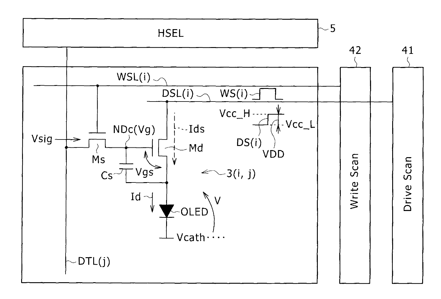
도 1에 나타내는 유기 EL디스플레이(1)는, 화소 어레이(2)를 포함한다. 화소 어레이(2)에는 복수의 화소회로(PXLC)(3)(i,j)가 매트릭스 모양으로 배치되어 있다. 유기 EL디스플레이(1)는 화소 어레이(2)를 구동하는 수직구동회로(V스캐너)(4) 및 수평구동회로(H셀렉터:HSEL)(5)를 더 포함한다.The
V스캐너(4)는, 화소회로(3)의 구성에 의해 복수 설치되어 있다. 여기에서는 V스캐너(4)가, 수평화소 라인 구동회로(Drive Scan)(41)와, 기록 신호 주사 회로(Write Scan)(42)를 포함하여 구성되어 있다. V스캐너(4) 및 H셀렉터(5)는 「구동회로」의 일부이며, 「구동회로」는, V스캐너(4)와 H셀렉터(5) 외에, 이것들에 클록 신호를 주는 회로나 제어회로(CPU 등) 등, 도시하지 않은 회로도 포함한다.
도 1에 나타내는 화소회로의 부호 「3(i,j)」은, 이 화소회로가 수직방향(세로방향)의 어드레스 i(i=1,2)와, 수평방향(가로방향)의 어드레스 j(j=1,2,3)를 갖는 것을 의미한다. 이들 어드레스 i와 j는 최대값을 각각 「n」과 「m」으로 하는 1 이상의 정수를 취한다. 여기에서는 도면을 간략화하기 위해 n=2, m=3인 경우를 나타낸다.(I = 1, 2) in the vertical direction (vertical direction) and an address j (i, j) in the horizontal direction j = 1, 2, 3). These addresses i and j take one or more integers with the maximum value being " n " and " m ", respectively. Here, in order to simplify the drawing, n = 2 and m = 3 are shown.
이 어드레스 표기는, 이후의 설명이나 도면에 있어서 화소회로의 소자, 신호나 신호선 및 전압 등에 대해서도 마찬가지로 적용한다.This address notation is also applied to elements, signals, signal lines, and voltages of the pixel circuits in the following description and drawings.
화소회로 3(1,1), 3(2,1)이 수직방향의 영상 신호선 DTL(1)에 접속되어 있 다. 마찬가지로, 화소회로 3(1,2), 3(2,2)가 수직방향의 영상 신호선 DTL(2)에 접속되어 있다. 화소회로 3(1,3), 3(2,3)이 수직방향의 영상 신호선 DTL(3)에 접속되어 있다. 영상 신호선 DTL(1)∼ DTL(3)은, H셀렉터(5)에 의해 구동된다.The pixel circuits 3 (1, 1), 3 (2, 1) are connected to the vertical video signal line DTL (1). Similarly, the pixel circuits 3 (1, 2) and 3 (2, 2) are connected to the vertical video signal line DTL (2). The pixel circuits 3 (1, 3), 3 (2, 3) are connected to the vertical video signal line DTL (3). The video signal lines DTL (1) to DTL (3) are driven by the H selector (5).
제1행의 화소회로 3(1,1), 3(1,2) 및 3(1,3)이 기록 주사선 WSL(1)에 접속되어 있다. 마찬가지로, 제2행의 화소회로 3(2,1), 3(2,2) 및 3(2,3)이 기록 주사선 WSL(2)에 접속되어 있다. 기록 주사선 WSL(1), WSL(2)는, 기록 신호 주사 회로(42)에 의해 구동된다.The pixel circuits 3 (1, 1), 3 (1, 2) and 3 (1, 3) in the first row are connected to the recording scanning line WSL (1). Similarly, the pixel circuits 3 (2,1), 3 (2,2) and 3 (2,3) in the second row are connected to the recording scan line WSL (2). The write scan lines WSL (1) and WSL (2) are driven by the write
또한 제1행의 화소회로 3(1,1), 3(1,2) 및 3(1,3)이 전원 주사선 DSL(1)에 접속되어 있다. 마찬가지로, 제2행의 화소회로 3(2,1), 3(2,2) 및 3(2,3)이 전원 주사선 DSL(2)에 접속되어 있다. 전원 주사선 DSL(1), DSL(2)는, 수평화소 라인 구동회로(41)에 의해 구동된다.In addition, the pixel circuits 3 (1, 1), 3 (1, 2) and 3 (1, 3) in the first row are connected to the power supply scanning line DSL (1). Similarly, the pixel circuits 3 (2,1), 3 (2,2) and 3 (2,3) in the second row are connected to the power supply scanning line DSL (2). The power supply scanning lines DSL (1) and DSL (2) are driven by the horizontal pixel
영상 신호선 DTL(1)∼ DTL(3)을 포함하는 m개의 영상 신호선 중 어느 하나 1개를, 이하, 부호 「DTL(j)」로 표기한다. 마찬가지로, 기록 주사선 WSL(1), WSL(2)를 포함하는 n개의 기록 주사선 중 어느 1개를 부호 「WSL(i)」로 표기하고, 전원 주사선 DSL(1),DSL(2)를 포함하는 n개의 전원 주사선 중 어느 1개를 부호 「DSL(i)」로 표기한다.One of the m video signal lines including the video signal lines DTL (1) to DTL (3) will hereinafter be referred to as "DTL (j)". Likewise, any one of n recording scanning lines including the recording scanning lines WSL (1) and WSL (2) is denoted by the sign " WSL (i) " One of the n power supply scanning lines is denoted by the symbol " DSL (i) ".
본 실시예에서는, 선 순차 구동 또는, 점 순차 구동을 사용할 수 있다. 선 순차 구동에서는, 영상 신호선 DTL(j)에 대하여, 표시 화소 행(표시 라인이라고도 한다)을 단위로 동시에 영상 신호가 공급된다. 점 순차 구동에서는, 동일 행의 영상 신호선 DTL(j)에 차례로, 영상 신호가 공급된다.In the present embodiment, line-sequential drive or dot-sequential drive can be used. In the line-sequential driving, a video signal is simultaneously supplied to the video signal line DTL (j) in units of display pixel rows (also referred to as display lines). In the dot sequential driving, video signals are sequentially supplied to the video signal lines DTL (j) in the same row.
<화소회로><Pixel circuit>
도 2에, 화소회로(3)(i,j)의 일 구성예를 나타낸다.Fig. 2 shows an exemplary configuration of the pixel circuit 3 (i, j).
도 2에 나타내는 화소회로(3)(i,j)는, 유기발광 다이오드 OLED를 제어하는 회로이다. 화소회로는, 유기발광 다이오드 OLED 외에, 구동 트랜지스터 Md 및 샘플링 트랜지스터 Ms와, 하나의 유지 커패시터 Cs를 갖는다. 구동 트랜지스터 Md 및 샘플링 트랜지스터 Ms는 각각 NMOS TFT를 포함한다.The pixel circuit 3 (i, j) shown in Fig. 2 is a circuit for controlling the organic light emitting diode OLED. The pixel circuit has, in addition to the organic light emitting diode OLED, a driving transistor Md, a sampling transistor Ms, and one holding capacitor Cs. The driving transistor Md and the sampling transistor Ms each include an NMOS TFT.
유기발광 다이오드 OLED는, 특별히 도시하지 않지만, 예를 들면 상면 발광 표시의 경우 다음과 같이 형성된다. 우선, 투명 유리 등으로 이루어지는 기판에 형성된 TFT구조 위에 애노드 전극을 형성한다. 다음에, 정공 수송층, 발광층, 전자 수송층, 전자 주입층 등을 순차 퇴적시켜서 유기 다층막을 구성하는 적층체를 애노드 전극 위에 형성한다. 마지막으로, 적층체 위에 투명전극재료로 이루어지는 캐소드 전극을 형성한다. 애노드 전극은 양극 전원에 접속되고, 캐소드 전극은 음극 전원에 접속된다.Although not specifically shown, the organic light emitting diode OLED is formed, for example, in the case of a top emission display as follows. First, an anode electrode is formed on a TFT structure formed on a substrate made of transparent glass or the like. Next, a laminate constituting the organic multilayer film is formed on the anode electrode by successively depositing a hole transporting layer, a light emitting layer, an electron transporting layer, and an electron injecting layer. Finally, a cathode electrode made of a transparent electrode material is formed on the laminate. The anode electrode is connected to the anode power source, and the cathode electrode is connected to the cathode power source.
유기발광 다이오드 OLED의 애노드와 캐소드의 전극 간에 소정의 전계가 얻어지는 바이어스 전압을 인가하면, 주입된 전자와 정공이 발광층에서 재결합할 때 유기 다층막이 자발광한다. 유기발광 다이오드 OLED는, 유기 다층막을 구성하는 유기재료를 적절히 선택하는 것으로 빨강(R), 초록(G), 파랑(B)의 각 색에서의 발광이 가능하다. 따라서 이 유기재료를, 예를 들면 각 행의 화소에 R, G, B의 발광이 가능하게 배열하는 것으로, 컬러 표시가 가능하게 된다. 또는, 백색발광의 유기재료를 사용하여, 필터의 색으로 R, G, B의 구별을 행해도 된다. 또는, R, G, B 외에 W(화이트)를 추가한 4색 구성이어도 된다.When a bias voltage for obtaining a predetermined electric field is applied between the anode and the cathode of the organic light emitting diode OLED, the organic multilayer film self-luminesces when the injected electrons and holes are recombined in the light emitting layer. The organic light emitting diode OLED can emit light in red (R), green (G), and blue (B) colors by appropriately selecting an organic material constituting the organic multilayer film. Therefore, color display can be achieved by arranging the organic material so as to emit R, G, and B in pixels of each row, for example. Alternatively, the organic material of white light emission may be used to distinguish R, G, and B from the color of the filter. Alternatively, a four-color configuration in which W (white) is added in addition to R, G, and B may be used.
구동 트랜지스터 Md는, 유기발광 다이오드 OLED에 흐르는 전류량을 제어하여 표시 계조를 규정하는 전류제어수단으로서 기능한다.The driving transistor Md functions as current control means for controlling the amount of current flowing through the organic light emitting diode OLED to define the display gradation.
구동 트랜지스터 Md의 드레인은, 전원전압 VDD의 공급을 제어하는 전원 주사선 DSL(i)에 접속된다. 구동 트랜지스터 Md의 소스는 유기발광 다이오드 OLED의 애노드에 접속된다.The drain of the driving transistor Md is connected to the power supply scanning line DSL (i) for controlling the supply of the power supply voltage VDD. The source of the driving transistor Md is connected to the anode of the organic light emitting diode OLED.
샘플링 트랜지스터 Ms는, 데이터 전위 Vsig의 공급선(영상 신호선 DTL(j))과 구동 트랜지스터 Md의 게이트(제어 노드 NDc) 사이에 접속되어 있다. 데이터 전위 Vsig는 화소 계조를 결정한다. 샘플링 트랜지스터 Ms의 소스와 드레인의 한쪽이 구동 트랜지스터 Md의 게이트(제어 노드 NDc)에 접속되고, 나머지 한쪽이 영상 신호선 DTL(j)에 접속되어 있다. 영상 신호선 DTL(j)에, H셀렉터(5)(도 1 참조)로부터 데이터 전위 Vsig를 갖는 데이터 펄스가 소정의 간격으로 공급된다. 샘플링 트랜지스터 Ms는, 데이터 전위의 공급 기간(데이터 펄스의 지속시간(duration time))의 적정한 타이밍에, 이 화소회로에서 표시해야 할 레벨의 데이터를 샘플링한다. 이것은, 레벨이 불안정한 천이기간 동안 표시 영상에 주는 영향을 배제하기 위함이다. 레벨은 샘플링해야 할 원하는 데이터 전위 Vsig를 갖는 데이터 펄스의 전단 또는 후단에서 불안정하다.The sampling transistor Ms is connected between the supply line (video signal line DTL (j)) of the data potential Vsig and the gate (control node NDc) of the driving transistor Md. The data potential Vsig determines the pixel gradation. One of the source and the drain of the sampling transistor Ms is connected to the gate of the driving transistor Md (control node NDc), and the other is connected to the video signal line DTL (j). Data pulses having a data potential Vsig are supplied to the video signal line DTL (j) at a predetermined interval from the H selector 5 (see Fig. 1). The sampling transistor Ms samples data of a level to be displayed in this pixel circuit at a proper timing of the supply period of the data potential (the duration of the data pulse). This is to exclude the influence of the level on the display image during the unstable transition period. Level is unstable at the front end or the rear end of the data pulse having the desired data potential Vsig to be sampled.
구동 트랜지스터 Md의 게이트와 소스(유기발광 다이오드 OLED의 애노드) 사이에, 유지 커패시터 Cs가 접속되어 있다. 유지 커패시터 Cs의 역할에 대해서는, 후술의 동작 설명으로 명백하게 한다.A holding capacitor Cs is connected between the gate of the driving transistor Md and the source (the anode of the organic light emitting diode OLED). The role of the storage capacitor Cs will be clarified in the following description of the operation.
도 2에서는, 수평화소 라인 구동회로(41)에 의해, 전원구동 펄스 DS(i)가 구동 트랜지스터 Md의 드레인에 공급된다. 전원구동 펄스 DS(i)는 파고치가 전원전압 VDD이 되는 고전위 Vcc_H와 기준전위 또는 저전위 Vcc_L를 갖는다. 구동 트랜지스터 Md의 보정시나 유기발광 다이오드 OLED의 발광시에 전원공급이 행해진다.In Fig. 2, the horizontal pixel
또한 기록 신호 주사 회로(42)에 의해, 비교적 짧은 지속시간의 기록 구동 펄스 WS(i)가 샘플링 트랜지스터 Ms의 게이트에 공급되어, 샘플링 제어가 행해진다.Further, the recording
이 때, 전원공급의 제어는, 구동 트랜지스터 Md의 드레인과 전원전압 VDD의 공급선 사이에 트랜지스터를 하나 더 삽입하고, 그 게이트를 수평화소 라인 구동회로(41)에 의해 제어하는 구성으로 해도 된다(후술의 변형예 참조).The power supply may be controlled by inserting another transistor between the drain of the driving transistor Md and the supply line of the power supply voltage VDD and controlling the gate thereof by the horizontal pixel
도 2에서는 유기발광 다이오드 OLED의 애노드가 구동 트랜지스터 Md를 통해 양측의 전원으로부터 전원전압 VDD의 공급을 받고, 유기발광 다이오드 OLED의 캐소드가 캐소드 전위 Vcath를 공급하는 소정의 전압선(음측의 전원선)에 접속되어 있다.2, the anode of the organic light emitting diode OLED receives supply voltage VDD from the power supplies on both sides through the driving transistor Md, and the cathode of the organic light emitting diode OLED is connected to a predetermined voltage line (power supply line on the negative side) for supplying the cathode potential Vcath Respectively.
통상, 화소회로 내의 모든 트랜지스터는 TFT로 형성되어 있다. TFT의 채널이 형성되는 박막반도체층은, 다결정 실리콘 또는 아모퍼스 실리콘 등의 반도체 재료로 이루어진다. 폴리실리콘 TFT는 이동도를 높게 취하지만 특성 변동이 크기 때문에, 표시장치의 대화면화에 적합하지 않다. 따라서, 대화면을 갖는 표시장치로는, 일반적으로, 아모퍼스 실리콘 TFT가 이용된다. 다만, 아모퍼스 실리콘 TFT로는 P채널형 TFT가 형성되기 어렵다. 그러므로 전술한 화소회로(3)(i,j)와 같이, 모든 TFT 를 N채널형으로 하는 것이 바람직하다.Normally, all the transistors in the pixel circuit are formed of TFTs. The thin film semiconductor layer in which the channel of the TFT is formed is made of a semiconductor material such as polycrystalline silicon or amorphous silicon. The polysilicon TFT has a high mobility but a large variation in characteristics, and thus is not suitable for a large-screen display device. Therefore, in general, an amorphous silicon TFT is used as a display device having a large surface. However, it is difficult to form a P-channel TFT with the amorphous silicon TFT. Therefore, as with the pixel circuit 3 (i, j) described above, it is preferable that all the TFTs are of the N-channel type.
여기에서, 이상의 화소회로(3)(i,j)는, 본 실시예에서 적용가능한 화소회로의 일례, 즉 2트랜지스터(2T)·1커패시터(1C)형의 기본 구성예이다. 따라서, 본 실시예에서 이용할 수 있는 화소회로는, 상기 화소회로(3)(i,j)를 기본구성으로 하고, 또한 트랜지스터나 커패시터를 부가한 화소회로여도 된다(후술의 변형예 참조). 또한 기본구성에 있어서, 유지 커패시터 Cs를 전원전압 VDD의 공급선과 구동 트랜지스터 Md의 게이트 사이에 접속하는 경우도 있다.Here, the above-described pixel circuits 3 (i, j) are an example of a pixel circuit applicable in the present embodiment, that is, a basic configuration example of a 2-transistor (2T) 1 capacitor (1C) type. Therefore, the pixel circuit which can be used in the present embodiment may be a pixel circuit in which the pixel circuit 3 (i, j) has the basic structure and a transistor or a capacitor is added (see a modified example described later). Further, in the basic configuration, the storage capacitor Cs may be connected between the supply line of the power supply voltage VDD and the gate of the driving transistor Md.
구체적으로, 본 실시예에서 채용가능한 2T·1C형 이외의 화소회로로서, 후술하는 변형예로 몇 가지를 간단히 서술하지만, 예를 들면 4T·1C형, 4T·2C형, 5T·1C형, 3T·1C형 등이어도 된다.Specifically, some of the pixel circuits other than the 2T and 1C types that can be employed in the present embodiment will be briefly described as modified examples to be described later. For example, 4T and 1C type, 4T and 2C type, 5T and 1C type, and 3T 1C type or the like.
도 2의 구성을 기본으로 하는 화소회로에서는, 임계값전압 보정시나 이동도 보정시에 유기발광 다이오드 OLED를 역 바이어스 하면, 등가 용량값이 유지 커패시터 Cs의 값보다 충분히 커진다. 그 결과 유기발광 다이오드 OLED의 애노드가 전위적으로 거의 고정되어, 보정 정밀도가 향상된다. 따라서 유기발광 다이오드 OLED를 역 바이어스 한 상태에서 보정을 행하는 것이 바람직하다.In the pixel circuit based on the configuration of FIG. 2, if the organic light emitting diode OLED is reverse biased at the time of threshold voltage correction or mobility correction, the equivalent capacitance value becomes sufficiently larger than the value of the holding capacitor Cs. As a result, the anode of the organic light emitting diode OLED is almost fixed potentially, and the correction accuracy is improved. Therefore, it is preferable to carry out the correction while the organic light emitting diode OLED is reverse-biased.
캐소드 전위 Vcath를 접지하지 않고, 캐소드를 소정의 전압선에 접속하고 있는 것은, 역 바이어스를 행하기 위함이다. 유기발광 다이오드 OLED를 역 바이어스 하기 위해서는, 예를 들면 전원구동 펄스 DS(i)의 기준전위(저전위 Vcc_L)보다, 캐소드 전위 Vcath를 크게 한다.The reason why the cathode is connected to the predetermined voltage line without grounding the cathode potential Vcath is that reverse bias is performed. In order to reverse bias the organic light emitting diode OLED, for example, the cathode potential Vcath is made larger than the reference potential (low potential Vcc_L) of the power source drive pulse DS (i).
<표시 제어><Display Control>
도 2의 회로에 있어서의 데이터 기록시의 동작을, 임계값전압과 이동도의 보정동작과 함께 설명한다. 이들 일련의 동작을 「표시 제어」라고 한다.The operation at the time of data recording in the circuit of Fig. 2 will be described together with the correction operation of the threshold voltage and the mobility. These series of operations are referred to as " display control ".
최초에, 보정대상이 되는 구동 트랜지스터와 유기발광 다이오드 OLED의 특성에 대하여 설명한다.First, the characteristics of the driving transistor and the organic light emitting diode OLED to be corrected will be described.
도 2에 나타내는 구동 트랜지스터 Md의 제어 노드 NDc에는, 유지 커패시터 Cs가 결합되어 있다. 영상 신호선 DTL(j)을 통해 전송되는 데이터 펄스의 데이터 전위 Vsig가 샘플링 트랜지스터 Ms에 의해 샘플링된다. 얻어진 데이터 전위는 제어 노드 NDc에 인가되고, 유지 커패시터 Cs에 의해 유지된다. 구동 트랜지스터 Md의 게이트에 소정의 전위가 인가되었을 때, 그 드레인 전류 Ids는, 인가전위에 따른 값을 갖는 게이트 소스간 전압 Vgs에 의해 정해진다.A holding capacitor Cs is coupled to the control node NDc of the driving transistor Md shown in Fig. The data potential Vsig of the data pulse transmitted through the video signal line DTL (j) is sampled by the sampling transistor Ms. The obtained data potential is applied to the control node NDc and held by the holding capacitor Cs. When a predetermined potential is applied to the gate of the driving transistor Md, the drain current Ids is determined by the gate-source voltage Vgs having a value corresponding to the applied potential.
여기에서 구동 트랜지스터 Md의 소스 전위 Vs를, 상기 데이터 펄스의 기준전위(데이터 기준전위 Vo)로 초기화한 후, 샘플링을 행한다. 드레인 전류 Ids가 구동 트랜지스터 Md를 통해 흐른다. 드레인 전류 Ids는 샘플링 후의 데이터 전위 Vsig, 더 정확하게는, 데이터 기준전위 Vo와 데이터 전위 Vsig의 전위차로 규정되는 데이터 전압 Vin의 크기에 따른다. 드레인 전류 Ids는 거의 유기발광 다이오드 OLED의 구동전류 Id의 역할을 한다.Here, the source potential Vs of the driving transistor Md is initialized to the reference potential (data reference potential Vo) of the data pulse, and then sampling is performed. The drain current Ids flows through the driving transistor Md. The drain current Ids depends on the data potential Vsig after sampling, more precisely the magnitude of the data voltage Vin defined by the potential difference between the data reference potential Vo and the data potential Vsig. The drain current Ids substantially acts as the driving current Id of the organic light emitting diode OLED.
따라서, 구동 트랜지스터 Md의 소스 전위 Vs가 데이터 기준전위 Vo로 초기화되어 있는 경우, 유기발광 다이오드 OLED가 데이터 전위 Vsig에 따른 휘도로 발광한다.Therefore, when the source potential Vs of the driving transistor Md is initialized to the data reference potential Vo, the organic light emitting diode OLED emits light with a luminance corresponding to the data potential Vsig.
도 3에, 유기발광 다이오드 OLED의 I-V 특성의 그래프와, 구동 트랜지스터 Md의 드레인 전류 Ids(OLED의 구동전류 Id에 거의 상당)의 일반식을 나타낸다.3 shows a general expression of a graph of the I-V characteristic of the organic light emitting diode OLED and a drain current Ids of the driving transistor Md (substantially corresponding to the driving current Id of the OLED).
유기발광 다이오드 OLED는, 잘 알려진 바와 같이, 경시 변화에 의해 I-V 특성이 도 3과 같이 변화된다. 이때, 도 2의 화소회로에서는, 구동 트랜지스터 Md가 일정한 드레인 전류 Ids를 흐르게 하려 해도, 도 3에 나타내는 그래프에서 알 수 있는 바와 같이 유기발광 다이오드 OLED의 인가전압이 커지기 때문에, 유기발광 다이오드 OLED의 소스 전위 Vs가 상승한다. 이때 구동 트랜지스터 Md의 게이트는 플로팅 상태다. 따라서 거의 일정한 게이트 소스간 전압 Vgs가 유지되도록, 소스 전위의 상승과 함께 게이트 전위도 상승한다. 이는 유기발광 다이오드 OLED의 발광 휘도를 변화시키지 않도록 작용한다.As is well known, the organic light emitting diode OLED changes in I-V characteristics with time as shown in Fig. At this time, in the pixel circuit of FIG. 2, even if the driving transistor Md attempts to cause a constant drain current Ids to flow, since the voltage applied to the organic light emitting diode OLED increases as shown in the graph of FIG. 3, The potential Vs rises. At this time, the gate of the driving transistor Md is in a floating state. Therefore, the gate potential also rises with the rise of the source potential so that the substantially constant gate-source voltage Vgs is maintained. This serves not to change the emission luminance of the organic light emitting diode OLED.
그러나 화소회로마다 구동 트랜지스터 Md의 임계값전압 Vth, 이동도 μ가 다르다. 이에 따라, 도 3의 식에 따라, 드레인 전류 Ids에 편차가 생긴다. 그 결과 표시 화면 내에서 주어지고 있는 데이터 전위 Vsig가 같은 2개의 화소라도, 이 2개의 화소간에서 발광 휘도가 다르다.However, the threshold voltage Vth and the mobility μ of the driving transistor Md are different for each pixel circuit. As a result, the drain current Ids varies in accordance with the equation shown in Fig. As a result, even if there are two pixels having the same data potential Vsig given in the display screen, the light emission luminance differs between these two pixels.
도 3의 식에 있어서, 부호 "Ids"는, 포화 영역에서 동작하는 구동 트랜지스터 Md의 드레인과 소스 간에 흐르는 전류를 나타낸다. 또한 구동 트랜지스터 Md에 있어서, "Vth"가 임계값전압을, "μ"가 이동도를, "W"가 실효 채널 폭(실효 게이트 폭)을, "L"이 실효 채널길이(실효 게이트 길이)를, 각각 나타낸다. 또한 "Cox"가 구동 트랜지스터 Md의 단위 게이트 용량, 즉 단위면적당 게이트 산화막 용량과, 소스/드레인과 게이트 간의 프린징(fringing) 용량의 총합을 나타낸다.3, reference character "Ids " indicates a current flowing between the drain and the source of the driving transistor Md operating in the saturation region. In the driving transistor Md, "Vth" is the threshold voltage, "μ" is the mobility, "W" is the effective channel width (effective gate width), "L" is the effective channel length (effective gate length) Respectively. "Cox" represents the sum of the unit gate capacitance of the driving transistor Md, that is, the gate oxide film capacitance per unit area, and the fringing capacitance between the source / drain and the gate.
N채널형의 구동 트랜지스터 Md를 갖는 화소회로는, 구동능력이 높고 제조 프 로세스를 간략화할 수 있는 이점이 있다. 그러나 임계값전압 Vth이나 이동도 μ의 편차를 억제하기 위해, 임계값전압 Vth이나 이동도 μ의 보정동작을 발광 가능한 바이어스 설정에 앞서 행할 필요가 있다.The pixel circuit having the N-channel type driving transistor Md has an advantage in that the driving capability is high and the manufacturing process can be simplified. However, in order to suppress the deviation of the threshold voltage Vth and the mobility μ, it is necessary to perform the correction operation of the threshold voltage Vth and the mobility μ prior to the bias setting capable of emitting light.
도 4a∼도 4e는, 표시 제어에 있어서의 각종 신호나 전압의 파형을 나타내는 타이밍 차트다. 여기에서의 표시 제어에서는 행 단위로 데이터 기록을 순차 행하는 것으로 한다. 도 4a∼도 4e에서는, 제1행의 화소회로(3)(1,j)가 기록 대상의 행(표시 라인)이며, 제1행의 표시 라인에 대하여, 필드 F(1)에 있어서 표시 제어를 행할 경우를 나타내고 있다. 이 때, 도 4a∼도 4e에서는, 그것보다 앞의 필드 F(0)의 제어에 대해서는, 그 일부(발광 정지의 제어)를 나타내고 있다.4A to 4E are timing charts showing waveforms of various signals and voltages in display control. In the display control here, it is assumed that data recording is sequentially performed in units of rows. 4A to 4E show that the pixel circuits 3 (1, j) of the first row are the rows (display lines) of the object of recording and the display control of the display control of the field F Is performed. At this time, in FIGS. 4A to 4E, the control of the field F (0) ahead of it shows a part (control of stopping the light emission).
도 4a는, 영상 신호 Ssig의 파형도이다. 도 4b는, 기록 대상의 표시 라인에 공급되는 기록 구동 펄스 WS의 파형도이다. 도 4c는, 기록 대상의 표시 라인에 공급되는 전원구동 펄스 DS의 파형도이다. 도 4d는, 기록 대상의 표시 라인에 속하는 하나의 화소회로(3)(1,j)에 있어서의 구동 트랜지스터 Md의 게이트 전위 Vg(제어 노드 NDc의 전위)의 파형도이다. 도 4e는, 기록 대상의 표시 라인에 속하는 하나의 화소회로(3)(1,j)에 있어서의 구동 트랜지스터 Md의 소스 전위 Vs(유기발광 다이오드 OLED의 애노드 전위)의 파형도이다.4A is a waveform diagram of the video signal Ssig. 4B is a waveform diagram of the recording drive pulse WS supplied to the display line to be recorded. 4C is a waveform diagram of the power supply driving pulse DS supplied to the display line of the recording object. FIG. 4D is a waveform diagram of the gate potential Vg (potential of the control node NDc) of the drive transistor Md in one pixel circuit 3 (1, j) belonging to the display line to be written. 4E is a waveform diagram of the source potential Vs (anode potential of the organic light emitting diode OLED) of the driving transistor Md in one pixel circuit 3 (1, j) belonging to the display line of the recording object.
[기간의 정의][Definition of Period]
도 4a의 상부에 기재하고 있는 바와 같이, 처리 추이는 다음과 같다. 즉, 1필드(또는 프레임) 앞 화면의 발광 허가 기간(LM(0)) 뒤에 시계열 순으로, 앞 화면의 발광 정지 기간(LM-STOP), 「더미 Vth 보정」을 행하는 더미 Vth 보정기 간(VTCO), 「보정준비」를 행하는 초기화 기간(INT), 「임계값전압 보정의 본 동작」을 행하는 임계값전압 보정기간(VTC), 기록&이동도 보정기간(W&μ)을 거쳐, 이 제1행의 화소회로(3)(1,j)의 발광 허가 기간(LM(1))으로 이어진다.As shown in the upper part of Fig. 4A, the processing trend is as follows. That is, a dummy Vth compensator (VTCO) for performing the "dummy Vth correction" for the light emission stop period (LM-STOP) and the dummy Vth correction of the previous screen in a time series order after the light emission permission period (LM ), A threshold voltage correction period (VTC) for performing " main operation of threshold voltage correction ", and a recording & mobility correction period (W & (1) of the pixel circuit 3 (1, j) of the pixel circuit 3 (1, j).
[구동 펄스의 개략][Outline of drive pulse]
도 4a∼도 4e에서는, 파형도의 적절한 개소에 시간표시를 부호 "T0C, T0D, T10, T11, …, T19, T1A, T1B, … ,T1D"에 의해 나타내고 있다. 시간 "T0C, T0D"가 필드 F(0)에 대응한다. 시간 "T10∼T1D"이 필드 F(1)에 대응한다.In FIGS. 4A to 4E, the time display is indicated by the signs "T0C, T0D, T10, T11, ..., T19, T1A, T1B, ..., T1D" at appropriate positions of the waveform diagram. The time "T0C, T0D" corresponds to the field F (0). The time "T10 to T1D" corresponds to the field F (1).
기록 구동 펄스 WS는, 도 4b에 나타내는 바와 같이, "L"레벨에서 비액티브, "H"레벨에서 액티브인 소정 수의 샘플링 펄스 SP0∼SPe를 포함한다. 샘플링 펄스 SP0과 SP1의 출현 주기는 일정하다. 그러나 샘플링 펄스 SP1과 SPe 사이에 샘플링 펄스는 출현하지 않는다. 3개의 샘플링 펄스 중, 샘플링 펄스 SP1만, 그 후에 출현하는 기록 펄스 WP와 중첩되어 있다. 이와 같이, 샘플링 펄스 SP0∼SPe와 기록 펄스 WP에 의해 기록 구동 펄스 WS가 구성된다.The write drive pulse WS includes a predetermined number of sampling pulses SP0 to SPe which are active at the "L" level and inactive at the "H" level, as shown in Fig. The appearance frequencies of the sampling pulses SP0 and SP1 are constant. However, no sampling pulse appears between the sampling pulses SP1 and SPe. Of the three sampling pulses, only the sampling pulse SP1 is superimposed on the recording pulse WP appearing thereafter. Thus, the sampling pulses SP0 to SPe and the recording pulse WP constitute the recording drive pulse WS.
영상 신호 Ssig는 m개(수백∼천 수백 개)의 영상 신호선 DTL(j)(도 1 및 도 2 참조)에 공급된다. 그 영상 신호 Ssig는 선 순차 표시에서는 m개의 영상 신호선 DTL(j)에 동시에 공급된다. 영상 신호 Ssig의 샘플링 후에 얻어지는 데이터 전압을 반영한 신호 진폭 Vin은, 도 4a에 나타내는 바와 같이, 데이터 기준전위 Vo를 기준으로 한 영상 신호 펄스 PP의 파고치에 상당한다. 이하, 신호 진폭 Vin을 데이터 전압 Vin이라고 부른다.The video signal Ssig is supplied to m (hundreds to several hundreds) video signal lines DTL (j) (see Figs. 1 and 2). The video signal Ssig is simultaneously supplied to the m video signal lines DTL (j) in the line-sequential display. The signal amplitude Vin reflecting the data voltage obtained after sampling the video signal Ssig corresponds to the peak value of the video signal pulse PP based on the data reference potential Vo as shown in Fig. 4A. Hereinafter, the signal amplitude Vin is referred to as a data voltage Vin.
도 4a에 2개 나타내는 영상 신호 펄스 PP(2), PP(1) 중, 제1행에 있어서 중 요한 영상 신호 펄스는, 기록 펄스 WP와 시간적으로 겹치는 영상 신호 펄스 PP(1)이다. 영상 신호 펄스 PP(1)의 데이터 기준전위 Vo로부터의 파고치가, 도 4a 내지 4e에 나타내는 표시 제어로 표시하고자 하는(기록하고자 하는) 계조값, 즉 데이터 전압 Vin에 상당한다. 이 계조값(=Vin)은, 제1행의 각 화소에서 같은 경우(단색 표시의 경우)도 있다. 그러나 통상, 표시 화소 행의 계조값에 따라 변화한다.Of the two video signal pulses PP (2) and PP (1) shown in FIG. 4A, an important video signal pulse in the first row is a video signal pulse PP (1) temporally overlapping with the recording pulse WP. The peak value from the data reference potential Vo of the video signal pulse PP (1) corresponds to the gray scale value to be displayed (to be written) by display control shown in Figs. 4A to 4E, that is, the data voltage Vin. This gradation value (= Vin) is the same in each pixel of the first row (in the case of monochrome display). However, it usually varies according to the tone value of the display pixel row.
도 4a 내지 4e는, 주로, 제1행 내에 있어서의 하나의 화소에 관한 동작을 설명하기 위한 것이다. 그러나 동일 행의 다른 화소에서는, 이 표시 계조값이 다른 경우가 있는 외에, 제어 자체는, 나타내는 화소구동 제어와 시간을 어긋나게 하여 병렬로 실행된다.Figs. 4A to 4E are mainly for explaining operations relating to one pixel in the first row. Fig. However, in other pixels of the same row, the display gradation values may be different, and the control itself is executed in parallel with the pixel driving control being shifted in time from each other.
구동 트랜지스터 Md의 드레인(도 2 참조)에 공급되는 전원구동 펄스 DS의 전위는, 도 4c에 나타내는 바와 같이, 시간 T0C부터 더미 Vth 보정기간(VTCO)의 시작(시간 T10)까지 비액티브의 "L"레벨, 즉 저전위 Vcc_L로 유지된다. 전원구동 펄스 DS는 더미 Vth 보정기간(VTCO)의 시작과 거의 동시에(시간 T10), 액티브의 "H"레벨, 즉 고전위 Vcc_H로 추이한다. 전원구동 펄스 DS는 더미 Vth 보정기간(VTOC)의 종료(시간 T13)까지만 고전위 Vcc_H에 유지된다. 거기에서 시작되는 초기화 기간(INT, 시간 T13∼T16)에는, 전원구동 펄스 DS의 전위가 다시 저전위 Vcc_L로 되돌아간다. 전원구동 펄스 DS의 전위는, 시간 T16에 고전위 Vcc_H로 되돌아간 후, 발광 허가 기간(LM(1))이 종료될 때까지 계속된다.The potential of the power supply driving pulse DS supplied to the drain of the driving transistor Md (see FIG. 2) is inactive from the time T0C to the start of the dummy Vth correction period VTCO (time T10) Quot; level, that is, the low potential Vcc_L. The power supply driving pulse DS changes to the active "H" level, that is, to the high potential Vcc_H almost simultaneously with the start of the dummy Vth correction period VTCO (time T10). The power supply driving pulse DS is held at the high potential Vcc_H only until the end of the dummy Vth correction period VTOC (time T13). In the initialization period (INT, time T13 to T16) started there, the potential of the power supply driving pulse DS is returned to the low potential Vcc_L again. The potential of the power supply driving pulse DS is returned to the high potential Vcc_H at time T16, and continues until the light emission permission period LM (1) is ended.
본 실시예의 표시 제어에서는, 더미 Vth 보정기간(VTCO)이 존재한다. 본 실시예에 있어서, 이것을 다른 관점에서 말하면, 전원구동 펄스 DS의 전위가 모두 저 전위 Vcc_L인 발광 정지 기간(LM-STOP)과 초기화 기간(INT)을, 그 2개의 기간 사이에 더미 Vth 보정기간(VTCO)을 삽입함으로써 시간적으로 분리하는 것이다.In the display control of this embodiment, there is a dummy Vth correction period VTCO. In the present embodiment, from the other viewpoint, the light emission stop period (LM-STOP) and the initialization period (INT) in which the potential of the power supply driving pulse DS is all the low potential Vcc_L are divided into the dummy Vth correction period (VTCO).
최후의 샘플링 펄스 SPe는, 발광 정지 기간(LM-STOP)의 저전위 Vcc_L의 유지 기간 동안에 "L"레벨에서 "H"레벨로 추이한다. 한편 샘플링 펄스 SP1은, 초기화 기간(INT)의 저전위 Vcc_L의 유지 기간 동안에 "L"레벨에서 "H"레벨로 추이한다. 샘플링 펄스 SP1은, 초기화 기간(INT)이 종료되어 전원구동 펄스 DS의 전위가 고전위 Vcc_H로 유지되고 있는 기간 동안에 "H"레벨에서 "L"레벨로 추이한다.The last sampling pulse SPe changes from the "L" level to the "H" level during the sustain period of the low potential Vcc_L in the light emission stop period (LM-STOP). On the other hand, the sampling pulse SP1 changes from the "L" level to the "H" level during the sustain period of the low potential Vcc_L in the initialization period (INT). The sampling pulse SP1 shifts from the "H" level to the "L" level during the period in which the initialization period (INT) ends and the potential of the power supply driving pulse DS is maintained at the high potential Vcc_H.
이 때, 제2행(의 화소회로(3)(2,j)), 제3행(의 화소회로(3)(3,j))에 대해서는, 특별히 도면에는 나타내지 않았지만, 예를 들면 1수평기간씩 각 펄스(기록 구동 펄스 WS와 전원구동 펄스 DS)가 순차 지연되어 인가된다.At this time, although not shown in the drawings, for the pixel circuits (3, (2, j) in the second row and the pixel circuits (3, j) in the third row) And the respective pulses (the write drive pulse WS and the power supply drive pulse DS) are sequentially delayed and applied in periods.
따라서, 어느 행에 대하여 「임계값전압 보정」과 「기록 &이동도 보정」을 행하고 있는 기간에, 그것보다 앞의 행에 대해서는「더미 Vth 보정」이나 「초기화」가 실행된다. 그 결과, 「임계값전압 보정」과 「기록 &이동도 보정」만은 행 단위로 심리스(seamless)한 처리가 실행된다. 따라서, 불필요한 기간은 발생하지 않는다.Therefore, in a period during which "threshold voltage correction" and "recording and mobility correction" are performed for a certain row, "dummy Vth correction" and "initialization" are performed for rows before the threshold voltage correction and the recording and mobility correction. As a result, only "threshold voltage correction" and "recording and mobility correction" are seamlessly performed on a row-by-row basis. Therefore, an unnecessary period does not occur.
다음에, 이상의 펄스 제어하에 있어서의, 도 4d 및 도 4e에 나타내는 구동 트랜지스터 Md의 소스나 게이트의 전위변화와, 거기에 따르는 동작을, 도 4a에 나타내는 기간마다 설명한다.Next, the potential change of the source and gate of the driving transistor Md shown in Figs. 4D and 4E under the above-described pulse control and the operation thereunder will be described for each period shown in Fig. 4A.
이 때, 여기에서는 도 5a∼도 8b에 나타내는 제1행의 화소회로(3)(1,j)의 동작 설명도 및, 도 2 등을 적절히 참조한다.At this time, an operation explanatory diagram of the pixel circuit 3 (1, j) in the first row shown in Figs. 5A to 8B and Fig. 2 and the like are properly referred to.
[앞 화면의 발광 허가 기간(LM(0))][Light emission permission period (LM (0)) of the previous screen]
제1행의 화소회로(3)(1,j)에 대해, 시간 T0C 이전의 필드 F(0)(이하, 앞 화면이라고도 한다)에 있어서의 발광 허가 기간(LM(0))에는, 도 4b에 나타내는 바와 같이 기록 구동 펄스 WS가 "L"레벨이다. 그 결과, 샘플링 트랜지스터 Ms가 오프하고 있다. 이때 도 4c에 나타내는 바와 같이 전원구동 펄스 DS가 고전위 Vcc_H의 인가 상태에 있다.In the light emission permission period LM (0) in the field F (0) (hereinafter also referred to as the front screen) before the time T0C for the pixel circuit 3 (1, j) in the first row, The write drive pulse WS is at the "L" level. As a result, the sampling transistor Ms is off. At this time, as shown in FIG. 4C, the power supply drive pulse DS is in the application state of the high potential Vcc_H.
도 5a에 나타내는 바와 같이, 앞 화면의 데이터 기록 동작에 의해 구동 트랜지스터 Md의 게이트에 데이터 전압 Vin0이 입력되어 유지되고 있다. 이때 데이터 전압 Vin0에 따라, 유기발광 다이오드 OLED가 발광 상태에 있다고 하자. 구동 트랜지스터 Md는 포화 영역에서 동작하도록 설정되고 있다. 따라서 유기발광 다이오드 OLED에 흐르는 구동전류 Id(=Ids)는, 유지 커패시터 Cs로 유지되고 있는 구동 트랜지스터 Md의 게이트 소스간 전압 Vgs에 따라, 전술한 도 3에 나타내는 식으로부터 산출되는 값을 취한다.As shown in FIG. 5A, the data voltage Vin0 is input to the gate of the driving transistor Md and held by the data writing operation of the previous screen. At this time, it is assumed that the organic light emitting diode OLED is in a light emitting state according to the data voltage Vin0. The driving transistor Md is set to operate in the saturation region. Therefore, the driving current Id (= Ids) flowing through the organic light emitting diode OLED takes a value calculated from the above-described equation shown in Fig. 3 in accordance with the gate-source voltage Vgs of the driving transistor Md held in the holding capacitor Cs.
[발광 정지 기간(LM-STOP)] [Emission stop period (LM-STOP)]
도 4a 내지 4e에 있어서 시간 T0C에 발광 정지 처리가 시작된다.4A to 4E, the emission stop processing is started at time T0C.
시간 T0C이 되면, 수평화소 라인 구동회로(41)(도 2 참조)가, 도 4c에 나타내는 바와 같이, 전원구동 펄스 DS를 고전위 Vcc_H에서 저전위 Vcc_L로 전환한다. 구동 트랜지스터 Md에서는, 지금까지 드레인으로서 기능하고 있던 노드의 전위가 저전위 Vcc_L로까지 급격히 떨어진다. 그 결과 소스와 드레인의 전위가 역전된다. 이에 따라 지금까지 드레인이었던 노드를 소스로 하고, 지금까지 소스였던 노드를 드레인으로 하여, 이 드레인의 전하(단, 도면의 표기에서는 소스 전위 Vs 상태로 한다)를 방전하는 디스챠지 동작이 행해진다.At time T0C, the horizontal pixel line driving circuit 41 (see Fig. 2) switches the power supply driving pulse DS from the high potential Vcc_H to the low potential Vcc_L as shown in Fig. 4C. In the driving transistor Md, the potential of the node which has functioned as the drain so far drops sharply to the low potential Vcc_L. As a result, the potentials of the source and the drain are reversed. Thus, a discharging operation is performed in which the node that has been the drain until now is used as a source, the node that has been the source so far is used as a drain, and the charge of this drain (note that the source potential Vs is indicated in the drawing) is discharged.
따라서, 도 5b에 나타내는 바와 같이 지금까지와는 역방향의 드레인 전류 Ids가 구동 트랜지스터 Md에 흐른다.Therefore, as shown in Fig. 5B, the drain current Ids flowing in the reverse direction flows to the drive transistor Md so far.
발광 정지 기간(LM-STOP)이 시작되면, 도 4e에 나타내는 바와 같이, 시간 T0C을 경계로 구동 트랜지스터 Md의 소스 (실제동작에 있어 드레인)가 급격히 방전되고, 소스 전위 Vs가 저전위 Vcc_L의 근처까지 저하한다. 샘플링 트랜지스터 Ms의 게이트는 플로팅 상태이기 때문에, 소스 전위 Vs의 저하에 따라 게이트 전위 Vg도 저하한다.When the light emission stop period LM-STOP starts, as shown in Fig. 4E, the source (the drain in actual operation) of the drive transistor Md is rapidly discharged with the time T0C as a boundary, and the source potential Vs is low near the low potential Vcc_L . Since the gate of the sampling transistor Ms is in the floating state, the gate potential Vg also decreases with the decrease of the source potential Vs.
이때, 저전위 Vcc_L가 유기발광 다이오드 OLED의 발광 임계값전압 Vth_oled.과 캐소드 전위 Vcath의 합보다도 작을 때, 즉 "Vcc_L<Vth_oled.+Vcath"이면 유기발광 다이오드 OLED는 소광 한다.At this time, if the low potential Vcc_L is smaller than the sum of the emission threshold voltage Vth_oled. Of the organic light emitting diode OLED and the cathode potential Vcath, that is, "Vcc_L <Vth_oled. + Vcath", the organic light emitting diode OLED extinguishes.
다음에 기록 신호 주사 회로(42)(도 2 참조)가, 도 4b에 나타내는 바와 같이, 시간 T0D에서 기록 주사선 WSL(1)의 전위를 "L"레벨에서 "H"레벨로 천이시켜서 발생하는 샘플링 펄스 SP0를, 샘플링 트랜지스터 Ms의 게이트에 공급한다.Next, as shown in Fig. 4B, the recording signal scanning circuit 42 (see Fig. 2) performs a sampling operation in which the potential of the scanning scanning line WSL (1) is changed from the "L" The pulse SP0 is supplied to the gate of the sampling transistor Ms.
시간 T0D까지는, 영상 신호 Ssig의 전위가 데이터 기준전위 Vo로 전환된다. 따라서, 샘플링 트랜지스터 Ms는, 영상 신호 Ssig의 데이터 기준전위 Vo를 샘플링하고, 샘플링 후의 데이터 기준전위 Vo를 구동 트랜지스터 Md의 게이트에 전달한다.Up to time T0D, the potential of the video signal Ssig is switched to the data reference potential Vo. Therefore, the sampling transistor Ms samples the data reference potential Vo of the video signal Ssig and transfers the sampled data reference potential Vo to the gate of the driving transistor Md.
이 샘플링 동작에 의해, 도 4d 및 도 4e에 나타내는 바와 같이, 게이트 전위 Vg의 값이 데이터 기준전위 Vo에 수렴하고, 그것에 따라 소스 전위 Vs의 값은 저전위 Vcc_L에 수렴한다.By this sampling operation, as shown in Figs. 4D and 4E, the value of the gate potential Vg converges on the data reference potential Vo, and the value of the source potential Vs converges to the low potential Vcc_L accordingly.
여기에서 데이터 기준전위 Vo는, 전원구동 펄스 DS의 고전위 Vcc_H보다 낮고, 저전위 Vcc_L보다 높은 소정의 전위이다.Here, the data reference potential Vo is a predetermined potential lower than the high potential Vcc_H of the power source drive pulse DS and higher than the low potential Vcc_L.
이 샘플링 동작은, 후술하는 초기화와 같은 동작이다. 본 실시예에서는 샘플링 동작이 반드시 초기화를 실행할 필요는 없다. 대신, 샘플링 동작은 다음의 더미 Vth 보정의 동작을 시작할 수 있을 정도의 전위로 저하하기만 하면 된다.This sampling operation is the same as initialization described later. In the present embodiment, the sampling operation need not necessarily be initialized. Instead, the sampling operation only needs to be lowered to a potential enough to start the operation of the next dummy Vth correction.
초기화의 경우, 구동 트랜지스터 Md의 게이트 소스간 전압 Vgs가 구동 트랜지스터 Md의 임계값전압 Vth 이상이 되도록 전원구동 펄스 DS의 저전위 Vcc_L를 설정하고 있다. 구체적으로는, 도 5c에 나타내는 바와 같이, 게이트 전위 Vg가 데이터 기준전위 Vo가 되면, 이것에 연동해서 소스 전위 Vs가 전원구동 펄스 DS의 저전위 Vcc_L이 되므로, 유지 커패시터 Cs의 유지 전압이 저하하여, "Vo-Vcc_L"이 된다. 이 유지 전압 "Vo-Vcc_L"은 게이트 소스간 전압 Vgs 그 자체이다. 게이트 소스간 전압 Vgs가 구동 트랜지스터 Md의 임계값전압 Vth보다도 크지 않으면, 그 후에 임계값전압 보정동작을 행할 수 없다. 따라서 "Vo-Vcc_L>Vth"로 하도록 전위 관계가 정해져 있다.In the initialization, the low potential Vcc_L of the power supply driving pulse DS is set so that the gate-source voltage Vgs of the driving transistor Md is equal to or higher than the threshold voltage Vth of the driving transistor Md. Concretely, as shown in FIG. 5C, when the gate potential Vg becomes the data reference potential Vo, the source potential Vs becomes the low potential Vcc_L of the power source drive pulse DS in conjunction with this, so that the holding voltage of the holding capacitor Cs lowers , "Vo-Vcc_L ". This holding voltage "Vo-Vcc_L" is the gate-source voltage Vgs itself. If the gate-source voltage Vgs is not larger than the threshold voltage Vth of the driving transistor Md, the threshold voltage correction operation can not be performed thereafter. Therefore, the potential relationship is determined such that "Vo-Vcc_L > Vth ".
도 4b에 나타내는 최후의 샘플링 펄스 SPe는, 시간 T0D부터 충분한 시간이 경과한 시간에 종료하고, 샘플링 트랜지스터 Ms가 일단 오프한다.The last sampling pulse SPe shown in FIG. 4B ends at a time when a sufficient time has elapsed from the time T0D, and the sampling transistor Ms is once turned off.
그 후에 시간 T10에 필드 F(1)에 대한 처리가 시작된다.Then, at time T10, processing for field F (1) is started.
[더미 Vth 보정기간(VTCO)][Dummy Vth correction period (VTCO)]
시간 T10에는 도 4b에 나타내는 바와 같이 최초의 샘플링 펄스 SP0가 하이 레벨에 있고, 샘플링 트랜지스터 Ms가 온 하고 있다. 이 상태에서, 시간 T10에서 전원구동 펄스 DS의 전위가 저전위 Vcc_L에서 고전위 Vcc_H로 전환되고, 더미 Vth 보정기간(VTCO)이 시작된다.At time T10, as shown in Fig. 4B, the first sampling pulse SP0 is at the high level, and the sampling transistor Ms is turned on. In this state, the potential of the power supply driving pulse DS is switched from the low potential Vcc_L to the high potential Vcc_H at the time T10, and the dummy Vth correction period VTCO is started.
더미 Vth 보정기간(VTCO)의 시작시(시간 T10)의 직전에 있어서, 온 상태의 샘플링 트랜지스터 Ms가 데이터 기준전위 Vo를 샘플링하고 있는 상태이다. 따라서 도 6a에 나타내는 바와 같이 구동 트랜지스터 Md의 게이트 전위 Vg는, 일정한 데이터 기준전위 Vo에 전기적으로 고정된 상태에 있다.The sampling transistor Ms in the ON state is sampling the data reference potential Vo immediately before the start of the dummy Vth correction period VTCO (time T10). Therefore, as shown in Fig. 6A, the gate potential Vg of the driving transistor Md is in a state of being electrically fixed to a constant data reference potential Vo.
이 상태에서 시간 T10에, 전원구동 펄스 DS의 전위가 저전위 Vcc_L에서 고전위 Vcc_H로 천이하면, 구동 트랜지스터 Md의 소스와 드레인 간에 "전원구동 펄스 DS의 파고치에 상당하는 전압이 인가된다. 이에 따라 구동 트랜지스터 Md에 전원으로부터 드레인 전류 Ids가 흐르게 된다.In this state, when the potential of the power supply driving pulse DS transitions from the low potential Vcc_L to the high potential Vcc_H at time T10, a voltage corresponding to the peak value of the power supply driving pulse DS is applied between the source and the drain of the driving transistor Md. The drain current Ids flows from the power source to the driving transistor Md.
드레인 전류 Ids에 의해 구동 트랜지스터 Md의 소스가 충전되어, 도 4e에 나타내는 바와 같이 소스 전위 Vs가 상승한다. 따라서 그때까지 "Vo-Vcc_L"의 값을 취하고 있던 구동 트랜지스터 Md의 게이트 소스간 전압 Vgs(유지 커패시터 Cs의 유지 전압)는, 서서히 작아지게 된다(도 6a 참조).The source of the driving transistor Md is charged by the drain current Ids, and the source potential Vs rises as shown in Fig. 4E. Accordingly, until then the gate-source voltage Vgs (the holding voltage of the holding capacitor Cs) of the driving transistor Md taking the value of "Vo-Vcc_L" gradually decreases (see FIG. 6A).
게이트 소스간 전압 Vgs의 저하 속도가 빠를 경우, 도 4e에 나타내는 바와 같이 더미 Vth 보정기간(VTCO) 내에 소스 전위 Vs의 상승이 포화한다. 이 포화는 구동 트랜지스터 Md가 소스 전위 상승에 의해 컷오프하기 때문에 발생한다. 따라서, 게이트 소스간 전압 Vgs(유지 커패시터 Cs의 유지 전압)는, 구동 트랜지스터 Md의 임계값전압 Vth과 거의 같은 값으로 수렴한다.When the drop rate of the gate-source voltage Vgs is high, the rise of the source potential Vs is saturated within the dummy Vth correction period VTCO as shown in FIG. 4E. This saturation occurs because the driving transistor Md cuts off due to the rise of the source potential. Therefore, the gate-source voltage Vgs (the holding voltage of the holding capacitor Cs) converges to a value substantially equal to the threshold voltage Vth of the driving transistor Md.
이 때, 도 6a의 동작에서는, 구동 트랜지스터 Md를 흐르는 드레인 전류 Ids가 유지 커패시터 Cs의 한쪽 전극을 충전하는 외에, 유기발광 다이오드 OLED의 용량 Coled.를 충전한다. 이 때, 유기발광 다이오드 OLED의 용량 Coled.가 유지 커패시터 Cs보다 충분히 크다는 전제에서는, 드레인 전류 Ids의 대부분이 유지 커패시터 Cs의 충전에 사용된다. 그 경우, 게이트 소스간 전압 Vgs의 수렴점이 임계값전압 Vth와 거의 같은 값을 취한다.At this time, in the operation of FIG. 6A, the drain current Ids flowing through the driving transistor Md charges one electrode of the storage capacitor Cs and charges the capacitance Coled of the organic light emitting diode OLED. At this time, on the assumption that the capacitance Col.D of the organic light emitting diode OLED is sufficiently larger than the storage capacitor Cs, most of the drain current Ids is used for charging the storage capacitor Cs. In this case, the convergence point of the gate-source voltage Vgs takes a value substantially equal to the threshold voltage Vth.
상기 정확한 임계값전압 보정을 보증하기 위해서는, 용량 Coled.을 충분히 크게 할 의도로 유기발광 다이오드 OLED를 역 바이어스 하는 것이 바람직하다. 그러나 여기에서는 정확한 임계값전압 보정은 불필요하다. 따라서 유기발광 다이오드 OLED를 역 바이어스 하는 것은 필수는 아니다. 단, 유기발광 다이오드 OLED를 확실하게 소등하도록 캐소드 전위 Vcath가 정해지고 있다.In order to guarantee the accurate threshold voltage correction, it is preferable to reverse bias the organic light emitting diode OLED with an intention to increase the capacitance Coled. Sufficiently. However, accurate threshold voltage correction is not necessary here. Therefore, it is not necessary to reverse bias the organic light emitting diode OLED. However, the cathode potential Vcath is determined so as to reliably extinguish the organic light emitting diode OLED.
더미 Vth 보정기간(VTCO)은 시간 T13에 종료된다. 그러나 그 전의 시간 T11에 기록 구동 펄스 WS가 비액티브가 되어 샘플링 펄스 SP0가 종료된다. 이에 따라 도 6b에 나타내는 바와 같이, 샘플링 트랜지스터 Ms가 오프하고, 구동 트랜지스터 Md의 게이트가 플로팅 상태가 된다. 이때의 게이트 전위 Vg는 데이터 기준전위 Vo를 유지하고 있다.The dummy Vth correction period VTCO ends at time T13. However, the recording drive pulse WS becomes inactive at the time T11 before the end of the sampling pulse SP0. Thus, as shown in Fig. 6B, the sampling transistor Ms is turned off, and the gate of the driving transistor Md is in a floating state. At this time, the gate potential Vg maintains the data reference potential Vo.
샘플링 펄스 SP0가 시간 T11에 종료되고, 다음의 샘플링 펄스 SP1이 인가될 때까지(시간 T11∼T15), 영상 신호 펄스 PP(2)의 통과를 기다릴 필요가 있다. 영상 신호 펄스 PP(2)는 2행째의 데이터 기록에 필요하다.It is necessary to wait for the passage of the video signal pulse PP (2) until the sampling pulse SP0 ends at time T11 and the next sampling pulse SP1 is applied (time T11 to T15). The video signal pulse PP (2) is necessary for data recording in the second line.
[초기화 기간(INT)][Initialization period (INT)]
본 실시예에서는 샘플링 트랜지스터 Ms를 오프한 상태에서 전원구동 펄스 DS의 전위를 고전위 Vcc_H에서 저전위 Vcc_L로 전환하고, 이에 따라 초기화 기간(INT)이 시작된다.In the present embodiment, the potential of the power supply driving pulse DS is switched from the high potential Vcc_H to the low potential Vcc_L in a state in which the sampling transistor Ms is off, and accordingly the initialization period INT starts.
초기화에서는, 도 7a에 나타내는 바와 같이 전원구동 펄스 DS의 전위가 저전위 Vcc_L에 있다. 발광 정지 기간(LM-STOP)의 방전과 마찬가지로, 구동 트랜지스터 Md의 소스와 드레인이 교체된다. 이에 따라 구동 트랜지스터 Md가 온 하고, 소스(실제로는 드레인)의 전하가 방전되어, 소스 전위 Vs가 저전위 Vcc_L 부근까지 급속히 저하한다.In the initialization, as shown in Fig. 7A, the potential of the power supply driving pulse DS is at the low potential Vcc_L. The source and the drain of the driving transistor Md are replaced as in the case of the discharge in the light emission stop period LM-STOP. As a result, the driving transistor Md is turned on, the source (actually, the drain) is discharged, and the source potential Vs rapidly drops to the vicinity of the low potential Vcc_L.
소스 전위 Vs의 저하에 따라, 플로팅 상태의 게이트의 전위(Vg)도 저하한다. 이때, 소스 전위 Vs의 저하량이 그대로 게이트 전위 Vg의 저하량이 되지 않는다. 대신, 소정의 용량 결합비에 따라, 소스 전위 Vs의 저하량의 일부가 게이트 전위 Vg의 저하량이 된다. 따라서 유지 커패시터 Cs의 유지 전압은, 원래의 임계값전압 상당량보다 약간 커진다.As the source potential Vs decreases, the potential Vg of the gate in the floating state also decreases. At this time, the lowering amount of the source potential Vs does not become the lowering amount of the gate potential Vg as it is. Instead, a part of the lowering amount of the source potential Vs becomes the lowering amount of the gate potential Vg in accordance with the predetermined capacitive coupling ratio. Therefore, the holding voltage of the holding capacitor Cs becomes slightly larger than the original threshold voltage equivalent.
다음에 기록 신호 주사 회로(42)(도 2 참조)가, 도 4b에 나타내는 바와 같이, 시간 T15에 기록 구동 펄스 WS를 "L"레벨에서 "H"레벨로 전환시켜서 샘플링 펄스 SP1을, 샘플링 트랜지스터 Ms의 게이트에 공급한다.Next, the write signal scanning circuit 42 (see FIG. 2) switches the write drive pulse WS from the "L" level to the "H" level at time T15 to transfer the sampling pulse SP1 to the sampling transistor And supplies it to the gate of Ms.
시간 T15보다 앞선 시간 T14에, 영상 신호 펄스 PP(2)의 인가가 종료되고, 그 결과 영상 신호 Ssig의 전위가 데이터 기준전위 Vo로 전환된다. 따라서, 시간 T15에 온 하는 샘플링 트랜지스터 Ms는, 영상 신호 Ssig의 데이터 기준전위 Vo를 샘플링하여, 샘플링 후의 데이터 기준전위 Vo를 구동 트랜지스터 Md의 게이트에 전달한다.At a time T14 preceding the time T15, the application of the video signal pulse PP (2) is terminated, and as a result, the potential of the video signal Ssig is switched to the data reference potential Vo. Therefore, the sampling transistor Ms which is turned on at time T15 samples the data reference potential Vo of the video signal Ssig and transfers the sampled data reference potential Vo to the gate of the driving transistor Md.
이 샘플링 동작에 의해, 게이트 전위 Vg가 데이터 기준전위 Vo에 수렴한다. 이에 따라 소스 전위 Vs도 일단 상승한다. 그러나 구동트랜지스터 Md가 계속해서 온 상태에 있다. 그 결과 소스 전위 Vs는 저하하기 시작한다. 초기화 기간(INT)이 종료하는 시간 T16까지 소스 전위 Vs가 저전위 Vcc_L까지 저하하여, 구동 트랜지스터 Md는 오프한다.By this sampling operation, the gate potential Vg converges to the data reference potential Vo. As a result, the source potential Vs also rises once. However, the driving transistor Md is continuously turned on. As a result, the source potential Vs begins to decrease. The source potential Vs drops to the low potential Vcc_L until the time T16 at which the initialization period INT ends, and the driving transistor Md is turned off.
이상의 초기화동작에 있어서, 발광 정지 기간(LM-STOP)의 방전시와 마찬가지로 데이터 기준전위 Vo는, 전원구동 펄스 DS의 고전위 Vcc_H보다 낮고, 저전위 Vcc_L보다 높은 소정의 전위이다. 또한 "Vo-Vcc_L>Vth"로 하도록 전위관계가 정해져 있다. 이는 그 후에 임계값전압 보정동작을 실행할 수 있도록 보장하기 위한 것이다.In the above-described initializing operation, the data reference potential Vo is lower than the high potential Vcc_H of the power source drive pulse DS and is a predetermined potential higher than the low potential Vcc_L, as in the discharge in the light emission stop period LM-STOP. Quot; Vo-Vcc_L > Vth ". This is to ensure that the threshold voltage compensation operation can be performed thereafter.
초기화 동작에서는 유기발광 다이오드 OLED를 역 바이어스 하도록 캐소드 전위 Vcath가, 저전위 Vcc_L보다 높은 소정의 전위로 설정된다.In the initializing operation, the cathode potential Vcath is set to a predetermined potential higher than the low potential Vcc_L so as to reverse bias the organic light emitting diode OLED.
[임계값전압 보정기간(VTC)][Threshold voltage correction period (VTC)]
그 후에 시간 T16에 전원구동 펄스 DS의 전위가 저전위 Vcc_L에서 고전위 Vcc_H로 전환되면, 임계값전압 보정기간(VTC), 즉 임계값전압 보정의 본 동작이 시작된다. 임계값전압 보정기간(VTC)의 동작 자체는, 더미 Vth 보정기간(VTCO)에 대한 도 6a 및 도 6b와 같다.Thereafter, when the potential of the power supply driving pulse DS is switched from the low potential Vcc_L to the high potential Vcc_H at time T16, the threshold voltage correction period (VTC), that is, the main operation of the threshold voltage correction starts. The operation of the threshold voltage correction period VTC itself is the same as that of the dummy Vth correction period VTCO in Figs. 6A and 6B.
시간 T16의 시점에서 도 4b에 나타내는 바와 같이, 두 번째의 샘플링 펄스 SP1가 이미 하이 레벨에 있고, 샘플링 트랜지스터 Ms가 온 하고 있다. 이때문에, 도 6a와 마찬가지로, 구동 트랜지스터 Md의 게이트 전위 Vg는, 일정한 데이터 기준전위 Vo에 전기적으로 고정된 상태에 있다.At the time T16, as shown in Fig. 4B, the second sampling pulse SP1 is already at the high level, and the sampling transistor Ms is on. Therefore, as in Fig. 6A, the gate potential Vg of the driving transistor Md is in a state of being electrically fixed to a constant data reference potential Vo.
이 상태에서 시간 T16에, 전원구동 펄스 DS의 전위가 저전위 Vcc_L에서 고전위 Vcc_H로 전환되면, 구동 트랜지스터 Md의 소스와 드레인 간에 "전원구동 펄스 DS의 파고치에 상당하는 전압이 인가된다. 이에 따라 구동 트랜지스터 Md가 온 하여, 드레인 전류 Ids가 구동 트랜지스터 Md에 흐른다.In this state, when the potential of the power supply driving pulse DS is switched from the low potential Vcc_L to the high potential Vcc_H at time T16, a voltage corresponding to the peak value of the power supply driving pulse DS is applied between the source and the drain of the driving transistor Md. The driving transistor Md is turned on, and the drain current Ids flows to the driving transistor Md.
드레인 전류 Ids에 의해 구동 트랜지스터 Md의 소스가 충전되어, 도 4e에 나타내는 바와 같이 소스 전위 Vs가 상승한다. 따라서 그때까지 "Vo-Vcc_L"의 값을 취하고 있던 구동 트랜지스터 Md의 게이트 소스간 전압 Vgs(유지 커패시터 Cs의 유지 전압)는, 서서히 작아지게 된다(도 6a 참조).The source of the driving transistor Md is charged by the drain current Ids, and the source potential Vs rises as shown in Fig. 4E. Accordingly, until then the gate-source voltage Vgs (the holding voltage of the holding capacitor Cs) of the driving transistor Md taking the value of "Vo-Vcc_L" gradually decreases (see FIG. 6A).
게이트 소스간 전압 Vgs의 저하 속도가 빠를 경우, 도 4e에 나타내는 바와 같이, 더미 Vth 보정기간(VTCO) 내에 소스 전위 Vs의 상승이 포화한다. 이 포화는 구동 트랜지스터 Md가 소스 전위상승에 의해 컷오프하기 때문에 발생한다. 따라서, 게이트 소스간 전압 Vgs(유지 커패시터 Cs의 유지 전압)는, 구동 트랜지스터 Md의 임계값전압 Vth과 거의 같은 값으로 수렴한다.When the drop rate of the gate-source voltage Vgs is fast, the rise of the source potential Vs is saturated within the dummy Vth correction period VTCO as shown in FIG. 4E. This saturation occurs because the driving transistor Md cuts off due to the rise of the source potential. Therefore, the gate-source voltage Vgs (the holding voltage of the holding capacitor Cs) converges to a value substantially equal to the threshold voltage Vth of the driving transistor Md.
이 때, 도 6a의 동작에서는, 구동 트랜지스터 Md를 흐르는 드레인 전류 Ids가 유지 커패시터 Cs의 한쪽 전극을 충전하는 외에, 유기발광 다이오드 OLED의 용량 Coled.을 충전한다. 이때, 유기발광 다이오드 OLED의 용량 Coled.이 유지 커패시터 Cs보다 충분히 크다는 전제에서는, 드레인 전류 Ids의 대부분이 유지 커패시 터 Cs의 충전에 사용된다. 그 경우, 게이트 소스간 전압 Vgs의 수렴점이 임계값전압 Vth와 거의 같은 값을 취한다.At this time, in the operation of FIG. 6A, the drain current Ids flowing through the driving transistor Md charges one electrode of the storage capacitor Cs and charges the capacitance Coled of the organic light emitting diode OLED. At this time, on the premise that the capacitance of the organic light emitting diode OLED is sufficiently larger than the storage capacitor Cs, most of the drain current Ids is used for charging the storage capacitor Cs. In this case, the convergence point of the gate-source voltage Vgs takes a value substantially equal to the threshold voltage Vth.
상기 정확한 임계값전압 보정을 보증하기 위해, 임계값전압 보정기간(VTC)에서는, 유기발광 다이오드 OLED가 역 바이어스된 상태에서 임계값전압 보정을 행한다. 역 바이어스 상태에서는 유기발광 다이오드 OLED의 소등이 유지된다.In order to guarantee the accurate threshold voltage correction, in the threshold voltage correction period (VTC), the threshold voltage correction is performed while the organic light emitting diode OLED is reverse biased. In the reverse bias state, the light emission of the organic light emitting diode OLED is maintained.
임계값전압 보정기간(VTC)은 시간 T19에 종료된다. 그러나 그 전의 시간 T17에 기록 구동 펄스 WS가 비액티브로 되어 샘플링 펄스 SP1이 종료된다. 이에 따라 도 6b와 마찬가지로, 샘플링 트랜지스터 Ms가 오프하여, 구동 트랜지스터 Md의 게이트가 플로팅 상태가 된다. 이때의 게이트 전위 Vg는 데이터 기준전위 Vo를 유지하고 있다.The threshold voltage correction period VTC ends at time T19. However, the write drive pulse WS becomes inactive at the time T17 before this, and the sampling pulse SP1 is terminated. As a result, the sampling transistor Ms is turned off, and the gate of the driving transistor Md is in a floating state, as in Fig. 6B. At this time, the gate potential Vg maintains the data reference potential Vo.
시간 T17에 이어지는 시간 T18에 시간 T19까지, 영상 신호 펄스 PP(1)를 인가, 즉 영상 신호 Ssig의 전위를 데이터 전위 Vsig로 전환할 필요가 있다. 이것은, 시간 T19의 데이터 샘플링 시에 데이터 전위 Vsig가 안정된 소정 레벨이 되어, 데이터 전압 Vin을 정확하게 기록하기 위해, 데이터 전위 Vsig의 안정화를 기다리기 위함이다. 따라서 시간 T18∼T19의 길이는, 데이터 전위 안정화에 충분한 시간으로 설정되어 있다.It is necessary to apply the video signal pulse PP (1), that is, to turn the potential of the video signal Ssig to the data potential Vsig at time T18 following time T17 until time T19. This is to wait for stabilization of the data potential Vsig so that the data potential Vsig becomes a predetermined stable level at the time of data sampling at the time T19 and the data voltage Vin is accurately recorded. Therefore, the length of time T18 to T19 is set to a time sufficient for stabilizing the data potential.
[임계값전압 보정의 효과][Effect of threshold voltage correction]
여기에서 가령, 구동 트랜지스터의 게이트 소스간 전압이 "Vin"만큼 증가했다고 하면, 게이트 소스간 전압은 "Vin+Vth"가 된다. 한편 임계값전압 Vth이 큰 구동 트랜지스터와, 이것이 작은 구동 트랜지스터를 생각해본다.Assuming here that the gate-source voltage of the driving transistor is increased by "Vin ", the gate-source voltage becomes" Vin + Vth ". Consider a drive transistor having a large threshold voltage Vth and a drive transistor having a small threshold voltage Vth.
따라서 전자의 임계값전압 Vth이 큰 구동 트랜지스터는 소스간 전압이 크다. 역으로 임계값전압 Vth이 작은 구동 트랜지스터는 게이트 소스간 전압이 작다. 따라서, 임계값전압 Vth에 관해서 말하면, 임계값전압 보정동작에 의해, 임계값전압 Vth의 편차를 캔슬하면, 같은 데이터 전압 Vin에 대해 같은 드레인 전류 Ids를 구동 트랜지스터에 흘려보낼 수 있다.Therefore, the driving transistor having a large threshold voltage Vth of electrons has a large source-to-source voltage. Conversely, the driving transistor having a small threshold voltage Vth has a small gate-source voltage. Therefore, with respect to the threshold voltage Vth, if the deviation of the threshold voltage Vth is canceled by the threshold voltage correction operation, the same drain current Ids can be supplied to the drive transistor for the same data voltage Vin.
임계값전압 보정기간(VTC)에는, 드레인 전류 Ids가 오로지 유지 커패시터 Cs의 한쪽 전극측, 유기발광 다이오드 OLED의 용량 Coled.의 한쪽 전극 측으로 유입하는 데에만 소비되어, 유기발광 다이오드 OLED가 온 하지 않도록 할 필요가 있다. 유기발광 다이오드 OLED의 애노드 전압을 "Voled.", 그 발광 임계값전압을 "Vth_oled.", 그 캐소드 전위를 "Vcath"로 표기하면, 유기발광 다이오드 OLED를 오프 상태로 유지하는 조건은, "Voled.≤Vcath+Vth_oled."가 항상 성립하는 것이다.In the threshold voltage correction period (VTC), the drain current Ids is consumed solely to enter one electrode side of the storage capacitor Cs and one electrode side of the capacitance Coled. Of the organic light emitting diode OLED, so that the organic light emitting diode OLED does not turn on Needs to be. When the anode voltage of the organic light emitting diode OLED is represented as "Voled. &Quot;, the emission threshold voltage thereof is represented as Vth_oled., And the cathode potential thereof is represented as Vcath, the condition for keeping the organic light emitting diode OLED in the OFF state is & . Vcath + Vth_oled. "Is always established.
여기에서 유기발광 다이오드 OLED의 캐소드 전위 Vcath를 저전위 Vcc_L(예를 들면 접지 전압 GND)로 일정하게 했을 경우, 발광 임계값전압 Vth_oled.이 상당히 클 때에는, 이 식을 항상 성립시키는 것도 가능하다. 그러나 발광 임계값전압 Vth_oled.은 유기발광 다이오드 OLED의 제작 조건에 의해 결정된다. 또한 저전압으로 효율적인 발광을 위해서는 발광 임계값전압 Vth_oled.을 지나치게 크게 할 수 없다. 따라서, 본 실시예에서는 임계값전압 보정기간(VTC)이 종료할 때까지는, 캐소드 전위 Vcath를 저전위 Vcc_L보다 크게 설정함으로써, 유기발광 다이오드 OLED를 역 바이어스 시켜 둔다.Here, when the cathode potential Vcath of the organic light emitting diode OLED is made constant at the low potential Vcc_L (for example, the ground voltage GND), this formula can be always established when the emission threshold voltage Vth_oled. Is considerably large. However, the emission threshold voltage Vth_oled. Is determined by the manufacturing conditions of the organic light emitting diode OLED. Further, the emission threshold voltage Vth_oled. Can not be excessively increased for efficient light emission at a low voltage. Therefore, in this embodiment, the cathode potential Vcath is set to be higher than the low potential Vcc_L until the threshold voltage correction period VTC ends, thereby reversely biasing the organic light emitting diode OLED.
역 바이어스를 위한 캐소드 전위 Vcath는, 도 4a 내지 4e에 나타내는 기간 동안 계속해서 일정한 상태 그대로다. 다만, 더미 Vth 보정에 의해 역 바이어스가 해제되는 값으로, 캐소드 전위 Vcath의 일정 전위가 설정된다. 따라서, 임계값전압 보정시보다 소스 전위 Vs가 높아지는 시간 T19보다 후에, 역 바이어스가 해제된다. 이 상태에서 이동도 보정이나 발광을 위한 처리가 행해진다. 그 후의 발광 정지 처리로 다시 유기발광 다이오드 OLED가 역 바이어스 상태가 된다.The cathode potential Vcath for reverse bias continues to be constant during the period shown in Figs. 4A to 4E. However, a certain potential of the cathode potential Vcath is set to a value at which the reverse bias is released by the dummy Vth correction. Therefore, after the time T19 at which the source potential Vs becomes higher than that at the time of the threshold voltage correction, the reverse bias is released. In this state, processing for mobility correction or light emission is performed. And the organic light emitting diode OLED is again reverse-biased by the subsequent emission stop processing.
[기록&이동도 보정기간(W&μ)][Recording & mobility correction period (W &)]
시간 T19부터, 기록&이동도 보정기간(W&μ)이 시작된다. 이때의 상태는 도 6b와 동일하며, 샘플링 트랜지스터 Ms가 오프, 구동 트랜지스터 Md가 컷오프하고 있다. 구동 트랜지스터 Md의 게이트가 데이터 기준전위 Vo로 유지된다. 소스 전위 Vs가 "Vo-Vth", 게이트 소스간 전압 Vgs(유지 커패시터 Cs의 유지 전압)이 "Vth"로 되어 있다.From the time T19, the recording & mobility correction period (W &) starts. The state at this time is the same as in Fig. 6B, the sampling transistor Ms is off, and the driving transistor Md is cut off. The gate of the driving transistor Md is maintained at the data reference potential Vo. The source potential Vs is "Vo-Vth ", and the gate-source voltage Vgs (sustain voltage of the sustain capacitor Cs) is" Vth ".
도 4b에 나타내는 바와 같이, 영상 신호 펄스 PP(1)를 인가하고 있는 시간T19에, 기록 펄스 WP가 샘플링 트랜지스터 Ms의 게이트에 공급된다. 그러면 도 8a에 나타내는 바와 같이, 샘플링 트랜지스터 Ms가 온 하여, 데이터 전압 Vin이 구동 트랜지스터 Md의 게이트에 입력된다. 데이터 전압 Vin은 데이터 전위 Vsig(=Vin+Vo)와 게이트 전위 Vg(=Vo)의 차분이다. 그 결과, 게이트 전위 Vg가 "Vo+Vin"이 된다.As shown in Fig. 4B, at a time T19 during which the video signal pulse PP (1) is being applied, the recording pulse WP is supplied to the gate of the sampling transistor Ms. Then, as shown in Fig. 8A, the sampling transistor Ms is turned on, and the data voltage Vin is input to the gate of the driving transistor Md. The data voltage Vin is a difference between the data potential Vsig (= Vin + Vo) and the gate potential Vg (= Vo). As a result, the gate potential Vg becomes "Vo + Vin ".
게이트 전위 Vg가 데이터 전압 Vin만큼 상승하면, 이것에 연동해서 소스 전위 Vs도 상승한다. 이때, 데이터 전압 Vin이 그대로 소스 전위 Vs에 전달되는 것은 아니다. 대신, 용량결합비 g에 따른 비율의 변화만큼 ΔVs, 즉 "g*Vin"만큼 소스 전위 Vs가 상승한다. 이것을 다음 식(1)에 나타낸다.When the gate potential Vg rises by the data voltage Vin, the source potential Vs increases in conjunction with this. At this time, the data voltage Vin is not directly transferred to the source potential Vs. Instead, the source potential Vs rises by? Vs, that is, by "g * Vin" by the change of the ratio according to the capacitive coupling ratio g. This is shown in the following equation (1).
[수 1][Number 1]
ΔVs=Vin(=Vsig-Vo)×Cs/(Cs+Coled.)…(1)? Vs = Vin (= Vsig-Vo) Cs / (Cs + Coled.) ... (One)
여기에서 유지 커패시터 Cs의 용량값을 같은 부호 "Cs"로 나타낸다. 부호 "Coled."는 유기발광 다이오드 OLED의 등가 용량값이다.Here, the capacitance value of the holding capacitor Cs is denoted by the same sign "Cs ". The symbol "Coled." Is the equivalent capacitance value of the organic light emitting diode OLED.
이상으로부터, 이동도 보정을 고려하지 않으면, 변화 후의 소스 전위 Vs는 "Vo-Vth+g*Vin"이 된다. 그 결과, 구동 트랜지스터 Md의 게이트 소스간 전압 Vgs는, "(1-g)Vin+Vth"가 된다.From the above, without considering mobility correction, the source potential Vs after the change becomes "Vo-Vth + g * Vin ". As a result, the gate-source voltage Vgs of the driving transistor Md becomes "(1-g) Vin + Vth ".
여기에서, 이동도 μ에 의한 편차에 대하여 설명한다.Here, the deviation due to the mobility μ will be described.
앞에 행한 임계값전압 보정에서, 실제로는, 드레인 전류 Ids를 흘려보낼 때마다 이동도 μ에 의한 오차가 포함되어 있었다. 그러나 임계값전압 Vth의 편차가 크기 때문에 이동도 μ에 의한 오차성분을 엄밀하게 논의하지 않았다. 이때 용량결합비 g를 사용하지 않고, 간단히 "상승(up)"이나 "저하(down)"로 표기해서 설명한 것은, 이동도의 편차를 설명하는 것에 의한 번잡함을 회피하기 위함이다.In the threshold voltage correction performed before, actually, an error due to the mobility μ is included every time the drain current Ids is supplied. However, since the deviation of the threshold voltage Vth is large, the error component due to the mobility μ is not discussed in detail. The reason why the capacitive coupling ratio g is not used and which is simply described as "up" or " down "is described in order to avoid troubles caused by explaining the mobility deviation.
한편, 이미 설명했지만, 엄밀히 임계값전압 보정이 행해진 후에는, 유지 커패시터 Cs에 임계값전압 Vth가 유지되어 있다. 그 후에 구동 트랜지스터 Md를 온 시키면, 임계값전압 Vth의 대소에 의해 드레인 전류 Ids가 변동하지 않는다. 따라서 임계값전압 보정 후의 구동 트랜지스터 Md의 전도로, 가령, 이 전도시의 구동전류 Id에 의해 유지 커패시터 Cs의 유지 전압(게이트 소스간 전압 Vgs)의 값에 변동이 생겼다고 하면, 그 변동량 ΔV(양 또는 음의 극성을 취하는 것이 가능)은, 구동 트랜지스터 Md의 이동도 μ의 편차, 보다 엄밀하게는, 반도체 재료의 물성 파라미터인 순수한 의미에서의 이동도 외에, 트랜지스터의 구조상 혹은 제조 프로세스상에서 전류 구동력에 영향을 주는 요인의 종합적인 편차를 반영한 것이 된다.On the other hand, after the threshold voltage correction is strictly described, the threshold voltage Vth is held in the storage capacitor Cs. Then, when the driving transistor Md is turned on, the drain current Ids does not fluctuate due to the magnitude of the threshold voltage Vth. Therefore, when the value of the holding voltage (gate-source voltage Vgs) of the holding capacitor Cs is varied due to the conduction of the driving transistor Md after the threshold voltage correction, for example, by the driving current Id during the conduction, (Or negative polarity) can be taken as a deviation of the mobility μ of the drive transistor Md, more precisely the mobility in the pure sense which is the physical property parameter of the semiconductor material, And reflects the overall deviation of the factors that influence it.
이상을 근거로 한 후 동작 설명으로 되돌아가면, 도 8a에 있어서, 샘플링 트랜지스터 Ms가 온 하여 게이트 전위 Vg에 데이터 전압 Vin이 인가되었을 때, 구동 트랜지스터 Md는, 그 데이터 전압 Vin(계조값)에 따른 크기의 드레인 전류 Ids를 소스와 드레인 간에 흐르게 하고자 한다. 이때 드레인 전류 Ids가 이동도 μ에 따라 변동한다. 그 결과, 소스 전위 Vs는, "Vo-Vth+g*Vin"에 상기 이동도 μ에 의한 변동량 ΔV를 더한 "Vo-Vth+g*Vin+ΔV"가 된다.8A, when the sampling transistor Ms is turned on and the data voltage Vin is applied to the gate potential Vg, the driving transistor Md is turned on in response to the data voltage Vin (gray level value) So that the drain current Ids of the size can flow between the source and the drain. At this time, the drain current Ids fluctuates in accordance with the mobility μ. As a result, the source potential Vs becomes "Vo-Vth + g * Vin +? V" obtained by adding the fluctuation amount? V due to the above mobility μ to "Vo-Vth + g * Vin".
이 때 유기발광 다이오드 OLED를 발광시키지 않기 위해서는, "Vs(=Vo-Vth+g*Vin+ΔV)<Vth_oled.+Vcath"를 만족하도록, 데이터 전압 Vin이나 용량 결합비 g 등에 따른 캐소드 전위 Vcath를 미리 설정하면 된다.In order not to cause the organic light emitting diode OLED to emit light at this time, the cathode potential Vcath corresponding to the data voltage Vin, the capacitive coupling ratio g or the like is set to satisfy the relationship of "Vs (= Vo-Vth + g * Vin +? V) <Vth_oled. + Vcath" It may be set in advance.
캐소드 전위 Vcath를 미리 상기와 같이 설정하면, 유기발광 다이오드 OLED는 역 바이어스되어, 하이 임피던스 상태가 된다. 그 결과, 유기발광 다이오드 OLED는 다이오드 특성이 아닌 단순한 용량특성을 나타내게 된다.When the cathode potential Vcath is set in advance as described above, the organic light emitting diode OLED is reverse biased to a high impedance state. As a result, the organic light emitting diode OLED exhibits a simple capacitance characteristic rather than a diode characteristic.
이때 "Vs(=Vo-Vth+g*Vin+ΔV)<Vth_oled.+Vcath"의 식을 만족하는 한, 소스 전위 Vs는, 유기발광 다이오드 OLED의 발광 임계값전압 Vth_oled.과 캐소드 전위 Vcath의 합을 넘지 않는다. 따라서 드레인 전류 Ids(구동전류 Id)는 세 용량값을 가산한 용량 "C=Cs+Coled.+Cgs"를 충전하기 위해 사용된다. 이것들은 유지 커패시터 Cs의 용량값(같은 부호 Cs로 표기)과 유기발광 다이오드 OLED의 역 바이어스 시 등가용량의 용량값(기생 용량과 같은 부호 Coled.로 표기)과 구동 트랜지스터 Md의 게이트 소스 간에 존재하는 기생 용량의 용량값(Cgs로 표기)이다. 이에 따라 구동 트랜지스터 Md의 소스 전위 Vs는 상승해 간다. 이때, 구동 트랜지스터 Md의 임계값전압 보정동작은 이미 완료되어 있다. 따라서 구동 트랜지스터 Md가 흘려보내는 드레인 전류 Ids는 이동도 μ를 반영한 것이 된다.At this time, as long as the expression of "Vs (= Vo-Vth + g * Vin +? V) <Vth_oled. + Vcath" is satisfied, the source potential Vs is the sum of the emission threshold voltage Vth_oled. Of the organic light emitting diode OLED and the cathode potential Vcath . Therefore, the drain current Ids (drive current Id) is used to charge the capacitance "C = Cs + Coled. + Cgs " These are the capacitance values of the storage capacitor Cs (denoted by the same sign Cs) and the capacitance value of the equivalent capacitance at the time of reverse bias of the organic light emitting diode OLED (denoted by the same symbol Coled as parasitic capacitance) and the gate source of the driving transistor Md The capacitance value of the parasitic capacitance (denoted by Cgs). As a result, the source potential Vs of the driving transistor Md rises. At this time, the threshold voltage correction opening of the driving transistor Md has already been completed. Therefore, the drain current Ids flowing through the drive transistor Md reflects the mobility μ.
도 4d 및 도 4e에서 "(1-g)Vin+Vth-ΔV"의 식으로 나타내고 있는 바와 같이, 유지 커패시터 Cs에 유지되는 게이트 소스간 전압 Vgs에 있어서는, 소스 전위 Vs에 가산되는 변동량 ΔV가 임계값전압 보정 후에 게이트 소스간 전압 Vgs(=(1-g)Vin+Vth)으로부터 감산된다. 이에 따라 부귀환이 걸리도록 변동량 ΔV가 유지 커패시터 Cs에 유지된다. 따라서, 이하, 변동량 ΔV를 「부귀환량」이라고도 한다.As shown in the formulas (1-g) Vin + Vth-V in Figs. 4D and 4E, in the gate-source voltage Vgs held in the holding capacitor Cs, the variation? V added to the source potential Vs becomes Is subtracted from the gate-source voltage Vgs (= (1-g) Vin + Vth) after the value voltage correction. Thus, the fluctuation amount [Delta] V is held in the holding capacitor Cs so as to cause the negative feedback. Therefore, the fluctuation amount? V is hereinafter also referred to as " negative feedback amount ".
부귀환량 ΔV는 근사식 ΔV=t*Ids/(Coled.+Cs+Cgs)로 나타낼 수 있다. 이 근사식으로부터, 변동량 ΔV는 드레인 전류 Ids의 변동에 비례하여 변화하는 파라미터임을 알 수 있다.The amount of negative feedback ΔV can be expressed by the approximate expression ΔV = t * Ids / (Coled. + Cs + Cgs). From this approximate expression, it can be seen that the variation? V is a parameter that changes in proportion to the variation of the drain current Ids.
상기 부귀환량 ΔV의 식으로부터, 소스 전위 Vs에 부가되는 부귀환량 ΔV는, 드레인 전류 Ids의 크기(이 크기는, 데이터 전압 Vin의 크기, 즉 계조값과 양의 상관 관계에 있다)와, 드레인 전류 Ids가 흐르는 시간, 즉, 도 4b에 나타내는, 이동도 보정에 필요한 시간 T19에서 시간 T1A까지의 시간(t)에 의존하고 있다. 즉, 계조값이 클수록, 또한 시간(t)을 길게 취할수록, 부귀환량 ΔV가 커진다.From the formula of the negative feedback amount? V, the negative feedback amount? V to be added to the source potential Vs is the magnitude of the drain current Ids (this magnitude is in positive correlation with the magnitude of the data voltage Vin, (T) from the time T19 to the time T1A required for the mobility correction shown in Fig. 4B, that is, the time during which the drain current Ids flows. That is, the larger the gray level value and the longer the time t, the larger the negative feedback amount? V.
따라서, 이동도 보정의 시간(t)은 반드시 일정할 필요는 없다. 반대로 드레인 전류 Ids(계조값)에 따라 조정하는 것이 바람직한 경우가 있다. 예를 들면, 백 색 표시에 가깝고 드레인 전류 Ids가 클 경우, 이동도 보정의 시간(t)은 짧게 해야 한다. 반대로, 흑색 표시에 가까워지고 드레인 전류 Ids가 작아지면, 이동도 보정의 시간(t)을 길게 설정해야 한다. 계조값에 따른 이동도 보정시간의 자동조정은, 그 기능을 도 2에 나타내는 기록 신호 주사 회로(42) 등에 미리 설정함으로써 실현 가능하다.Therefore, the time t of mobility correction does not have to be constant. Conversely, it may be preferable to adjust it in accordance with the drain current Ids (tone value). For example, when the drain current Ids is close to the white color display, the time (t) of mobility correction must be shortened. On the other hand, if the display current approaches the black display and the drain current Ids decreases, the mobility correction time t must be set longer. The automatic adjustment of the mobility correction time in accordance with the tone value can be realized by presetting the function to the recording
[발광 허가 기간(LM(1))][Light emission permission period (LM (1))]
시간 T1A에 기록&이동도 보정기간(W&μ)이 종료되면, 발광 허가 기간(LM(1))이 시작된다.When the write & mobility correction period (W &) is ended at time T1A, the light emission permission period LM (1) starts.
시간 T1A에 기록 펄스 WP가 종료하므로, 샘플링 트랜지스터 Ms가 오프하고, 구동 트랜지스터 Md의 게이트가 전기적으로 플로팅 상태가 된다.Since the write pulse WP ends at time T1A, the sampling transistor Ms is turned off, and the gate of the drive transistor Md is electrically floating.
그러나 발광 허가 기간(LM(1)) 이전의 기록&이동도 보정기간(W&μ)에는, 구동 트랜지스터 Md는 데이터 전압 Vin에 따른 드레인 전류 Ids를 흘려보내려고 하지만, 실제로 흘려보낸다고는 할 수 없다. 그 이유는 다음과 같다. 즉, 유기발광 다이오드 OLED에 흐르는 전류값(Id)이 구동 트랜지스터 Md에 흐르는 전류값(Ids)에 비하여 매우 작으면, 샘플링 트랜지스터 Ms가 온 하고 있기 때문에, 구동 트랜지스터 Md의 게이트 전압 Vg는 "Vofs+Vin"에 고정된다. 소스 전위 Vs는 Vofs+Vin에서 임계값전압 Vth만큼 낮은 전위("Vofs+Vin-Vth")에 수렴하려고 한다. 따라서, 이동도 보정의 시간(t)을 아무리 길게 해도 소스 전위 Vs는 상기 수렴점을 초과하는 전위로는 되지 않는다. 이동도 보정은, 그 수렴까지의 속도 차이로 이동도 μ의 차이를 모니터하고, 보정하는 것이다. 이 때문에, 최대 휘도의 백색 표시의 데이터 전 압 Vin이 입력된 경우라도, 상기 수렴이 되기 전에 이동도 보정 시간(t)의 종점이 결정된다.However, in the write & mobility correction period W & before the emission permission period LM (1), the drive transistor Md tries to flow the drain current Ids corresponding to the data voltage Vin, but it can not be said to actually flow. The reason for this is as follows. That is, when the current value Id flowing through the organic light emitting diode OLED is very small compared with the current value Ids flowing through the driving transistor Md, the sampling transistor Ms is turned on, so that the gate voltage Vg of the driving transistor Md becomes "Vofs + Vin ". The source potential Vs tends to converge to a potential ("Vofs + Vin-Vth") which is lower than the threshold voltage Vth by Vofs + Vin. Therefore, even if the time t of mobility correction is long, the source potential Vs does not rise above the convergence point. The mobility correction is to monitor and correct the difference in mobility μ due to the speed difference up to the convergence. Therefore, even when the data voltage Vin of the white display of the maximum luminance is inputted, the end point of the mobility correction time t is determined before convergence.
발광 허가 기간(LM(1))이 시작되어 구동 트랜지스터 Md의 게이트가 플로팅이 되면, 그 소스 전위 Vs는, 더욱 상승 가능하게 된다. 따라서, 구동 트랜지스터 Md는, 입력된 데이터 전압 Vin에 따른 구동전류 Id를 흐르게 하도록 동작한다.When the emission permission period LM (1) is started and the gate of the driving transistor Md is floated, the source potential Vs thereof can be further raised. Therefore, the driving transistor Md operates to flow the driving current Id in accordance with the input data voltage Vin.
그 결과, 소스 전위 Vs(유기발광 다이오드 OLED의 애노드 전위)가 상승한다. 그 결과 도 8b에 나타내는 바와 같이, 드레인 전류 Ids가 구동전류 Id로서 유기발광 다이오드 OLED에 흐르기 시작하여, 유기발광 다이오드 OLED가 실제로 발광을 시작한다. 발광이 시작된 후 잠시 지나면, 구동 트랜지스터 Md는, 입력된 데이터 전압 Vin에 따른 드레인 전류 Ids로 포화한다. 드레인 전류 Ids(=Id)가 일정해지면, 유기발광 다이오드 OLED가 데이터 전압 Vin에 따른 휘도의 발광 상태가 된다.As a result, the source potential Vs (the anode potential of the organic light emitting diode OLED) rises. As a result, as shown in Fig. 8B, the drain current Ids starts to flow into the organic light emitting diode OLED as the drive current Id, and the organic light emitting diode OLED actually starts emitting light. After a lapse of a while after the start of light emission, the drive transistor Md saturates to the drain current Ids corresponding to the input data voltage Vin. When the drain current Ids (= Id) becomes constant, the organic light emitting diode OLED becomes a light emitting state of luminance corresponding to the data voltage Vin.
발광 허가 기간(LM(1))의 시작부터 휘도가 일정하게 될 때까지 유기발광 다이오드 OLED의 애노드 전위의 상승은, 구동 트랜지스터 Md의 소스 전위 Vs의 상승과 다름없다. 이 소스 전위 Vs의 상승은 유기발광 다이오드 OLED의 애노드 전압 Voled.의 상승량이라는 의미로 "ΔVoled."로 표기한다. 구동 트랜지스터 Md의 소스 전위 Vs는, "Vo-Vth+g*Vin+ΔV+ΔVoled."이 된다(도 4e 참조).The rise of the anode potential of the organic light emitting diode OLED is equal to the rise of the source potential Vs of the driving transistor Md until the luminance becomes constant from the start of the emission permission period LM (1). The rise of the source potential Vs is denoted by " DELTA VOLED. "In the sense of an increase in the anode voltage VolED. Of the organic light emitting diode OLED. The source potential Vs of the driving transistor Md becomes "Vo-Vth + g * Vin + DELTA V + DELTA Voled."
한편, 게이트 전위 Vg는, 게이트가 플로팅 상태이기 때문에, 도 4d에 나타내는 바와 같이, 소스 전위 Vs에 연동하여, 그 상승량 ΔVoled.만큼 상승한다. 드레인 전류 Ids의 포화에 따라 소스 전위 Vs가 포화하면, 게이트 전위 Vg도 포화한다.On the other hand, since the gate is in the floating state, the gate potential Vg increases by the amount of increase? Voled. In conjunction with the source potential Vs as shown in Fig. 4D. When the source potential Vs becomes saturated due to saturation of the drain current Ids, the gate potential Vg also becomes saturated.
그 결과, 게이트 소스간 전압 Vgs(유지 커패시터 Cs의 유지 전압)에 대해, 이동도 보정시의 값("(1-g)Vin+Vth-ΔV")이, 발광 허가 기간(LM(1)) 동안에도 유지된다.As a result, the value ("(1-g) Vin + Vth-? V") at the mobility correction is set to the light emission permission period LM (1) ≪ / RTI >
발광 허가 기간(LM(1))에는, 구동 트랜지스터 Md가 정전류원으로서 동작한다. 그 결과, 유기발광 다이오드 OLED의 I-V 특성이 경시 변화되고, 이것에 따라 구동 트랜지스터 Md의 소스 전위 Vs가 변화되는 경우가 있다.In the emission permission period LM (1), the drive transistor Md operates as a constant current source. As a result, the I-V characteristic of the organic light emitting diode OLED changes over time, and the source potential Vs of the driving transistor Md may change accordingly.
그러나, 유기발광 다이오드 OLED의 I-V 특성이 경시 변화의 유무에 관계없이, 유지 커패시터 Cs의 유지 전압이 ("(1-g)Vin+Vth-ΔV")으로 유지된다. 유지 커패시터 Cs의 유지 전압은, 구동 트랜지스터 Md의 임계값전압 Vth을 보정하는 성분(+Vth)과, 이동도 μ에 의한 변동을 보정하는 성분(-ΔV)을 포함한다. 따라서 임계값전압 Vth이나 이동도 μ가 다른 화소간에서 변동해도, 구동 트랜지스터 Md의 드레인 전류 Ids, 즉, 유기발광 다이오드 OLED의 구동전류 Id는 일정하게 유지된다.However, the holding voltage of the holding capacitor Cs is maintained at ((1-g) Vin + Vth -? V) regardless of whether the I-V characteristic of the organic light emitting diode OLED changes with the passage of time. The holding voltage of the holding capacitor Cs includes a component (+ Vth) for correcting the threshold voltage Vth of the driving transistor Md and a component (-ΔV) for correcting the variation due to the mobility μ. Therefore, even if the threshold voltage Vth or the mobility μ varies between pixels, the drain current Ids of the driving transistor Md, that is, the driving current Id of the organic light emitting diode OLED is kept constant.
구체적으로는, 구동 트랜지스터 Md는, 임계값전압 Vth이 클수록, 유지 커패시터 Cs에 의해 유지된 상기 전압에 포함된 임계값전압 보정성분을 사용해서 소스 전위 Vs를 낮춘다. 이는 드레인 전류 Ids(구동전류 Id)가 더 많이 흐르도록 소스 드레인간 전압을 크게 하기 위함이다. 따라서 임계값전압 Vth의 변동이 있어도 드레인 전류 Ids는 일정하게 유지된다.Specifically, as the threshold voltage Vth increases, the driving transistor Md lowers the source potential Vs by using the threshold voltage correction component included in the voltage held by the holding capacitor Cs. This is to increase the source drain voltage so that the drain current Ids (drive current Id) flows more. Therefore, even when the threshold voltage Vth fluctuates, the drain current Ids is kept constant.
한편, 이동도 μ가 작아 상기 변동량 ΔV가 작은 경우에는, 유지 커패시터 Cs의 유지 전압의 이동도 보정성분(-ΔV)에 의해 이 유지 전압의 저하량도 작아진다. 이에 따라, 상대적으로, 큰 소스 드레인간 전압이 확보된다. 그 결과, 구동 트 랜지스터 Md는 드레인 전류 Ids(구동전류 Id)를 더 많이 흐르게 하도록 동작한다. 따라서 이동도 μ의 변동이 있어도 드레인 전류 Ids는 일정하게 유지된다.On the other hand, when the mobility μ is small and the variation ΔV is small, the decrease amount of the holding voltage is also reduced by the mobility correction component (-ΔV) of the holding voltage of the holding capacitor Cs. As a result, a relatively large source drain voltage is secured. As a result, the drive transistor Md operates to further flow the drain current Ids (drive current Id). Therefore, the drain current Ids is kept constant even when the mobility μ fluctuates.
도 9a 내지 9c는, 세 가지 다른 상태 A, B, C에 있어서 데이터 전위 Vsig의 크기와 드레인 전류 Ids와의 관계(구동 트랜지스터 Md의 입출력 특성)의 변화를 모식적으로 나타낸다. 상태 A는 임계값전압과 이동도의 보정을 행하지 않는 초기 상태다. 상태 B는 임계값전압 보정만 행한 상태다. 상태 C는 임계값전압과 이동도의 보정을 행한 상태다.9A to 9C schematically show changes in the relationship (input / output characteristics of the driving transistor Md) between the magnitude of the data potential Vsig and the drain current Ids in three different states A, B, State A is an initial state in which the threshold voltage and mobility are not corrected. State B is the threshold voltage correction only. State C is a state in which the threshold voltage and mobility are corrected.
도 9a 내지 9c로부터, 크게 떨어져 있던 화소 A와 화소 B의 특성 커브가, 우선 임계값전압 보정으로 크게 가까워지고, 다음에 이동도 보정을 행하면 거의 같다고 생각되는 정도까지 다가갈 수 있다는 것을 알 수 있다.It can be seen from Figs. 9A to 9C that the characteristic curves of the pixel A and the pixel B largely separated from each other largely become close to the threshold voltage correction first, .
이상으로부터, 화소간에서 구동 트랜지스터 Md의 임계값전압 Vth나 이동도 μ가 변동해도, 또한, 구동 트랜지스터 Md의 특성이 경시 변화해도, 데이터 전압 Vin이 같은 한, 유기발광 다이오드 OLED의 발광 휘도도 일정하게 유지된다.From the above, even if the threshold voltage Vth or the mobility μ of the driving transistor Md fluctuates between pixels and the characteristic of the driving transistor Md changes over time, the light emission luminance of the organic light emitting diode OLED also becomes constant Lt; / RTI >
다음에, 본 실시예에서 더미 Vth 보정을 행하는 것에 의한 효과를, 더미 Vth 보정을 행하지 않는 경우를 비교예로 해서 설명한다.Next, the effect of performing the dummy Vth correction in this embodiment will be described as a comparative example in which the dummy Vth correction is not performed.
<비교예><Comparative Example>
도 10a∼도 10e는, 비교예의 발광 제어에 있어서의 각종 신호나 전압의 파형을 나타내는 타이밍 차트다. 도 10a∼도 10e에 있어서, 도 4a∼도 4e와 중복하는 신호, 시간, 전위변화 등은 모두 동일한 부호로 나타내고 있다. 따라서, 같은 부호에 관한 한, 지금까지의 설명은 본 비교예에 있어서도 적용된다. 이하, 도 10a∼도 10e의 제어가 도 4a∼도 4e의 제어와 다른 점만 설명한다.10A to 10E are timing charts showing the waveforms of various signals and voltages in the light emission control of the comparative example. In Figs. 10A to 10E, signals, time, potential changes, and the like overlapping with Figs. 4A to 4E are denoted by the same reference numerals. Therefore, as far as the same reference numerals are concerned, the description so far also applies to this comparative example. Hereinafter, only the points of difference in the control of Figs. 10A to 10E from those of Figs. 4A to 4E will be described.
도 10a∼도 10e를 도 4a∼도 4e와 비교하면 알 수 있는 바와 같이, 도 10a∼도 10e에 나타내는 제어에서는, 도 4a∼도 4e에 나타내는 제어에 있어서의 더미 Vth 보정기간(VTCO)과, 이것에 계속되는 초기화 기간(INT)을 생략한다. 따라서 도 10a∼도 10e에 나타내는 제어에서는, 필드 F(1)의 처리 시작과 동시에, 시간 T10부터 임계값 보정기간(VTC)을 시작하고 있다. 도 4a∼도 4e에 있어서의 시간 T10에는 샘플링 펄스 SP0이 활성 레벨이다. 도 10a∼도 10e에서는, 전술한 [임계값 보정기간(VTC)]의 설명을 그대로 적용하기 위한 시간 T10에는 샘플링 펄스 SP1이 활성 레벨이라고 하자. 전술한 [임계값 보정기간(VTC)]의 설명은, "시간 16"을 "시간 T10"으로 대체함으로써, 본 비교예에서도 중복 적용된다.10A to 10E are compared with Figs. 4A to 4E, in the control shown in Figs. 10A to 10E, the dummy Vth correction period VTCO in the control shown in Figs. 4A to 4E, And the following initialization period (INT) is omitted. Therefore, in the control shown in Figs. 10A to 10E, the threshold value correction period (VTC) starts at time T10 simultaneously with the start of the processing of the field F (1). At time T10 in Figs. 4A to 4E, the sampling pulse SP0 is at the active level. 10A to 10E, assume that the sampling pulse SP1 is at the active level at a time T10 for applying the description of the above-described [threshold correction period (VTC)] as it is. The description of the above-described [threshold value correction period (VTC)] is repeatedly applied even in this comparative example by replacing "time 16" with "time T10".
도 10a∼도 10e에 나타내는 제어에 있어서는, 필드 F(0)의 발광 정지 기간(LM-STOP)의 처리가, 도 4a∼도 4e에 있어서의 초기화 기간(INT)의 처리를 대신하는 것이다. 따라서, 임계값전압 보정의 본 동작(임계값 보정기간(VTC)의 처리)의 직전에 행하는 보정준비(초기화)는, 발광 정지 기간(LM-STOP)에 행해진다.In the control shown in Figs. 10A to 10E, the processing of the light emission stop period (LM-STOP) of the field F (0) replaces the processing of the initialization period INT in Figs. 4A to 4E. Therefore, the preparation for calibration (initialization) performed immediately before this operation (threshold value correction period VTC) of the threshold voltage correction is performed in the light emission stop period LM-STOP.
그러나, 발광 정지 기간(LM-STOP)은 유기 EL디스플레이(1)를 탑재한 시스템(기기)의 사양에 의해, 그 길이가 변경되는 경우가 있으며, 그것이 원인이 되어, 다음에 설명하는, 소위 "플래쉬 현상"이 생긴다.However, the length of the light emission stop period (LM-STOP) may vary depending on the specifications of the system (device) on which the
도 11a 및 11b는 플래쉬 현상의 원인을 설명하기 위한 도면이다.11A and 11B are views for explaining the cause of the flash phenomenon.
도 11a에는, 전원구동 펄스 DS의 파형을, 4필드(4F)에 걸쳐서 나타내고 있다. 도 10c에는 그 파형을 약 1필드(1F)만큼 나타내고 있다.In Fig. 11A, the waveform of the power supply driving pulse DS is shown over four fields (4F). In Fig. 10C, the waveform is shown by about one field (1F).
먼저 설명한 도 10a∼도 10e에 있어서, 발광 허가 기간(LM(0),LM(1))에 비해 임계값 보정기간(VTC), 기록&이동도 보정기간(W&μ)은 시간적으로 매우 짧다. 이 때문에, 도 11a에서는 임계값 보정기간(VTC)과 기록&이동도 보정기간(W&μ)의 도시를 생략한다. 1F 기간의 처음부터 발광 허가 기간(LM)이 시작되고 있다. 여기에서 발광 허가 기간(LM)은 전원구동 펄스 DS의 전위가 고전위 Vcc_H를 취하는 기간이다. 그 후에 전원구동 펄스 DS의 전위가 저전위 Vcc_L인 기간은 발광 정지 기간(LM-STOP)에 상당한다.10A to 10E described above, the threshold value correction period VTC and the recording and mobility correction period W & P are very short in terms of time as compared with the light emission permission periods LM (0) and LM (1). Therefore, the illustration of the threshold value correction period (VTC) and the recording and mobility correction period (W &) is omitted in FIG. 11A. The emission permission period LM is started from the beginning of the 1F period. Here, the emission permission period LM is a period in which the potential of the power supply driving pulse DS takes the high potential Vcc_H. The period in which the potential of the power supply driving pulse DS is at the low potential Vcc_L corresponds to the light emission stop period (LM-STOP).
도 11b에, 도 11a과 동기한 타이밍에서 변화되는 발광 강도 L를 모식적으로 나타내고 있다. 여기에서는 데이터 전압 Vin이 같은 화소 행을 4F 기간 연속 표시했을 경우를 나타내고 있다.Fig. 11B schematically shows the light emission intensity L which changes at the timing synchronized with Fig. 11A. Here, a case where a pixel row having the same data voltage Vin is continuously displayed for a period of 4F is shown.
도 11a에 나타내는 바와 같이, 최초의 2F 기간에는, 발광 정지 기간(LM-STOP)이 비교적 짧다. 그러나 그 후의 2F 기간에는 발광 정지 기간(LM-STOP)이 비교적 길다. 이 제어는, 예를 들면 기기를 옥외에서 옥내로 이동시킨 것 등에 대처하기 위한 것이다. 이에 대응하여 기기 내의 CPU나 다른 제어회로(도시하지 않음)가, 주변환경이 어두워졌다고 판단한다. 그 결과 CPU나 다른 제어회로는 시인성을 향상시키기 위해 표시의 밝기를 전체적으로 낮추는 경우가 있다. 동일한 처리는 기기가 저소비 전력 모드로 이행될 때 사용되는 경우도 있다. 한편, 유기발광 다이오드 OLED의 장수명화를 보장하기 위해 CPU나 다른 제어회로가 구동전류를 항상 일정하게 유지하는 경우가 있다. 예를 들면 데이터 전압 Vin이 클 때에는 구동전류가 지나치게 상승하는 것을 저지하기 위해 구동전류는 일정하게 유지하여, 발광 허가 기간(LM)을 길게 함으로써 상기 데이터 전압 Vin에 따른 발광 휘도의 확보를 행한다. 그 반대의 경우, 즉 도시하는 바와 같이 구동전류는 큰 값이고, 일정한 상태로 발광 허가 기간(LM)을 짧게 함에 따라, 데이터 전압 Vin의 저하에 대응하여 소정의 발광 휘도를 얻는 경우가 있다.As shown in Fig. 11A, in the first 2F period, the light emission stop period (LM-STOP) is relatively short. However, the light emission stop period (LM-STOP) is relatively long in the subsequent 2F period. This control is intended to cope with, for example, moving the device from outside to inside. Correspondingly, a CPU or another control circuit (not shown) in the apparatus judges that the surrounding environment is dark. As a result, the CPU or other control circuit may lower the brightness of the display as a whole to improve visibility. The same processing may be used when the apparatus is shifted to the low power consumption mode. On the other hand, in order to ensure the longevity of the organic light emitting diode OLED, a CPU or other control circuit may always keep the driving current constant. For example, when the data voltage Vin is large, the driving current is kept constant to prevent the driving current from rising excessively, and the emission luminance corresponding to the data voltage Vin is ensured by lengthening the emission permission period LM. In the opposite case, that is, as shown in the drawing, the drive current is a large value, and the predetermined light emission luminance may be obtained in response to the lowering of the data voltage Vin as the emission permission period LM is shortened in a constant state.
유기발광 다이오드 OLED에 역 바이어스가 걸리는 기간을 결정하는 것은 발광 정지 기간(LM-STOP)의 길이다. 따라서, 도시하는 바와 같이, 발광 허가 기간(LM)의 길이가 표시 도중에 전환되면, 그것에 따라 유기발광 다이오드 OLED에 실제로 역 바이어스가 걸리는 기간이 변화된다.The period during which the reverse bias is applied to the organic light emitting diode OLED is the length of the light emission stop period (LM-STOP). Therefore, as shown in the figure, when the length of the emission permission period LM is switched during the display, the period in which the reverse bias is actually applied to the organic light emitting diode OLED is changed accordingly.
유기발광 다이오드 OLED는, 역 바이어스를 인가하여 도 5a 등에 나타내는 용량 Coled.의 값이 안정될 때까지 시간이 걸린다. 이 시간은 1F 기간보다 길다. 또한, 천천히 용량값이 변화한다. 그 결과, 역 바이어스 기간이 길수록 용량 Coled.의 값이 커진다. 따라서 전술한 식 (1)로부터, 용량 Coled.의 값이 클수록 소스 전위 Vs의 변화분 ΔVs가 작아진다. 이에 따라 구동 트랜지스터 Md의 게이트 소스간 전압 Vgs가, 같은 데이터 전압 Vin을 입력하고 있었던 시간적으로 전의 다른 필드보다도 커진다. 이 게이트 소스간 전압 Vgs가 필드 간에서 커지면, 도 11c에 나타내는 바와 같이, 다음의 필드 표시로부터 발광 강도 L가 "ΔL"만큼 증대하여, 표시면 전체가 순간적으로 밝아지는 "플래쉬 현상"이 발생한다.It takes time to apply a reverse bias to the organic light emitting diode OLED until the value of the capacitance Col. is stabilized as shown in FIG. 5A or the like. This time is longer than the 1F period. Also, the capacitance value changes slowly. As a result, the longer the reverse bias period, the larger the value of the capacitance Coled. Therefore, from the above-mentioned equation (1), the larger the value of the capacitance Coled. Is, the smaller the change? Vs of the source potential Vs becomes. As a result, the gate-source voltage Vgs of the driving transistor Md becomes larger than the other field in time before the same data voltage Vin is inputted. When the gate-source voltage Vgs becomes larger between the fields, as shown in Fig. 11C, the light emission intensity L increases by DELTA L from the next field display, and a "flash phenomenon" occurs in which the entire display surface becomes instantaneously bright .
이와는 반대로, 발광 정지 기간(LM-STOP)이 갑자기 짧아지면, 역 바이어스 기간이 짧아진다. 따라서 상기와 반대의 이유로 게이트 소스간 전압 Vgs가 갑자기 작아진다. 그 결과 발광 강도 L가 낮아져 표시 화면이 순간적으로 어두워지는 현 상(플래쉬 현상의 일종)이 발생한다.On the other hand, if the light emission stop period (LM-STOP) suddenly becomes shorter, the reverse bias period becomes shorter. Therefore, the gate-source voltage Vgs suddenly becomes small for the reason opposite to the above. As a result, the light emission intensity L is lowered and the display screen instantaneously becomes dark (a kind of flash phenomenon) occurs.
상기 플래쉬 현상을 방지하기 위해, 본 실시예에 관련된 도 4a 내지 4e에 나타내는 표시 제어에서는, 시스템의 요구로 길이가 변동하는 경우가 있는 발광 정지 기간(LM-STOP)의 직후에 더미 Vth 보정기간(VTCO)을 설정한다. 그 후의 보정준비를 위해 설정되는 초기화 기간(INT)을 일정하게 하고 있다.In order to prevent the flash phenomenon, in the display control shown in Figs. 4A to 4E related to the present embodiment, the dummy Vth correction period (LM-STOP) is set immediately after the light emission stop period (LM-STOP) VTCO). The initialization period INT set for the subsequent preparation for correction is made constant.
임계값 보정기간(VTC)에는, 구동 트랜지스터 Md의 소스가 상승한다. 이에 따라 발광 정지 기간(LM-STOP) 동안 걸려있던 역 바이어스가 일단 해제된다. 그 후에 초기화 기간(INT)이 시작되는 동시에 새롭게 역 바이어스가 유기발광 다이오드 OLED에 인가된다. 따라서, 발광 강도 L에 영향을 주는 역 바이어스 기간은 항상 일정하게 되어, 전술한 플래쉬 현상이 효과적으로 방지된다.In the threshold value correction period VTC, the source of the driving transistor Md rises. As a result, the reverse bias applied during the light emission stop period LM-STOP is once released. Then, the initialization period (INT) starts and a new reverse bias is applied to the organic light emitting diode OLED. Therefore, the reverse bias period that affects the light emission intensity L is always constant, effectively preventing the aforementioned flash phenomenon.
이하 본 실시예에 있어서의 변형예를 서술한다.Modifications of this embodiment will be described below.
<변형예 1>≪ Modification Example 1 &
도 4a 내지 4e의 표시 제어에서는, 더미 Vth 보정기간(VTCO)을 1화면(1필드)의 최초에 행했다. 그러나 더미 Vth 보정기간은, 이것에 한정되지 않는다. 예를 들면 발광 허가 기간(LM)의 직후에 더미 Vth 보정을 행해도 된다.In the display control of Figs. 4A to 4E, the dummy Vth correction period VTCO is performed at the beginning of one screen (one field). However, the dummy Vth correction period is not limited to this. For example, the dummy Vth correction may be performed immediately after the emission permission period LM.
도 12a 내지 12e는, 발광 허가 기간 후에 더미 Vth 보정을 행할 경우의 설명도이다.12A to 12E are explanatory diagrams for a case in which dummy Vth correction is performed after the emission permission period.
도 12a 내지 12e의 표시 제어에서는, 발광 허가 기간(LM(0)) 후에 발광 정지 기간(LM-STOP)을 행하고, 그 직후에 더미 Vth 보정기간(VTCO)을 행하고 있다. 그 후에 비발광 상태가 계속된 후, 다음 필드 F(1)이 시작된다. 따라서 필드 F(1)의 초기에, 일정 기간의 초기화 기간(INT)이 진행된다. 초기화 기간(INT) 동안, 유기발광 다이오드 OLED는 역 바이어스된다. 그 후 임계값 보정기간(VTC), 기록&이동도 보정기간(W&μ), 발광 허가 기간(LM(1))이 계속된다.12A to 12E, the light emission stop period (LM-STOP) is performed after the light emission permission period (LM (0)), and the dummy Vth correction period (VTCO) is performed immediately thereafter. After that, after the non-emission state continues, the next field F (1) is started. Therefore, in the beginning of the field F (1), the initialization period INT of a certain period proceeds. During the initialization period INT, the organic light emitting diode OLED is reverse biased. Thereafter, the threshold value correction period VTC, the recording and mobility correction period W & mu, and the light emission permission period LM (1) are continued.
도 12a 내지 12e에 나타내는 변형예 1은, 발광 정지 기간(LM-STOP), 더미 Vth 보정기간(VTC0), 초기화 기간(INT), 임계값 보정기간(VTC), 기록&이동도 보정기간(W&μ), 발광 허가 기간(LM)의 순서로서는 전술한 도 4a 내지 4e의 경우와 같다.
<변형예 2>≪ Modification Example 2 &
화소회로는 도 2에 나타내는 것에 한정되지 않는다.The pixel circuit is not limited to the one shown in Fig.
도 2의 화소회로에서는 데이터 기준전위 Vo는 영상 신호 Ssig의 샘플링에 의해 주어진다. 그러나 데이터 기준전위 Vo를, 별도의 트랜지스터를 통해 구동 트랜지스터 Md의 소스나 게이트에 줄 수도 있다.In the pixel circuit of Fig. 2, the data reference potential Vo is given by sampling the video signal Ssig. However, the data reference potential Vo may be given to the source or gate of the driving transistor Md through a separate transistor.
도 2의 화소회로에서 커패시터는 유지 커패시터 Cs뿐이다. 그러나 다른 유지 커패시터를, 예를 들면 구동 트랜지스터 Md의 드레인과 게이트간에 또 하나 설치해도 된다.In the pixel circuit of Fig. 2, only the holding capacitor Cs is the capacitor. However, another holding capacitor may be provided, for example, between the drain and the gate of the driving transistor Md.
<변형예 3>≪
화소회로가 유기발광 다이오드 OLED의 발광과 비발광을 제어하는 구동방법에는, 화소회로 내의 트랜지스터를 주사선에 의해 제어하는 방법과, 전원전압의 공급선을 구동회로에 의해 AC구동하는 방법(전원 AC구동방법)이 있다.Driving methods in which the pixel circuit controls the light emission and non-light emission of the organic light emitting diode OLED include a method of controlling the transistors in the pixel circuit by scanning lines and a method of AC driving the power supply voltage supply line by a driving circuit ).
도 2의 화소회로는, 후자의 전원 AC구동방법의 일례다. 그러나 이 방법에 있 어서 유기발광 다이오드 OLED의 캐소드측을 AC구동하여 구동전류를 흘려보낼지 여부를 제어해도 된다.The pixel circuit of Fig. 2 is an example of the latter power AC driving method. However, in this method, the cathode side of the organic light emitting diode OLED may be AC driven to control whether or not the driving current should be passed.
한편, 전자의 발광 제어를 주사선에 의해 제어하는 방법에서는, 구동 트랜지스터 Md의 드레인측 또는, 소스와 유기발광 다이오드 OLED 사이에, 다른 트랜지스터를 삽입하고, 그 게이트를 전원구동제어의 주사선으로 구동한다.On the other hand, in the method of controlling the electron emission control by the scanning line, another transistor is inserted between the drain side of the driving transistor Md or between the source and the organic light emitting diode OLED, and the gate thereof is driven by the scanning line of power supply driving control.
<변형예 4><
도 4a 내지 4e에 나타내는 표시 제어는, 임계값 보정기간(VTC)을 1회의 보정으로 행한다. 그러나 복수 회의 연속된(초기화를 사이에 두지 않는다는 의미) 처리로 임계값 보정을 행해도 된다.The display control shown in Figs. 4A to 4E performs the threshold correction period (VTC) by one correction. However, the threshold value correction may be performed by a plurality of consecutive processes (meaning that no initialization is performed).
그 경우, 초기화를 사이에 두지 않는다. 따라서 전원구동 펄스 DS의 전위를 최초의 임계값 보정시에 저전위 Vcc_L에서 고전위 Vcc_H로 높인 후에는, 발광 정지까지 고전위 Vcc_H가 유지된다. 이 점에서, 연속한 처리에 의한 임계값 보정동작은, 더미 Vth 보정과 임계값 보정의 본 동작 사이에 전원구동 펄스 DS의 전위를 저전위 Vcc_L로 일시적으로 낮추는, 도 4a 내지 4e에 나타내는 본 실시예의 동작과 근본적으로 다르다.In this case, no initialization is performed. Therefore, after the potential of the power supply driving pulse DS is raised from the low potential Vcc_L to the high potential Vcc_H at the time of the first threshold value correction, the high potential Vcc_H is maintained until the emission stops. 4A to 4E in which the potential of the power supply driving pulse DS is temporarily lowered to the low potential Vcc_L between the dummy Vth correction and the threshold current correction operation in this point, It is fundamentally different from motion.
<변형예 5>≪ Modified Example 5 &
도 4a 내지 4e에 나타내는 표시 제어에서는 더미 Vth 보정동작은 1회이다. 그러나 소스 충전 속도가 느리기 때문에 1회의 더미 Vth 보정으로는 역 바이어스뿐만 아니라 변동도 충분히 해제할 수 없는 경우, 상기 변형예 4의 「연속한 처리에 의한 임계값 보정동작」과 마찬가지로, 전원구동 펄스 DS의 전위를 고전위 Vcc_H로 유지한 채 더미 Vth 보정을 연속해서 복수 회 행해도 된다.In the display control shown in Figs. 4A to 4E, the dummy Vth correction is small once. However, since the source charging speed is slow, not only the reverse bias but also the fluctuation can not be sufficiently canceled by one time dummy Vth correction, similarly to the "threshold correction operation by continuous processing" of the fourth modification, The dummy Vth correction may be performed a plurality of times in succession while maintaining the potential at the high potential Vcc_H.
본 발명의 실시예에 의하면, 동일한 데이터 전압이 입력되는 한 모든 필드에 대한 휘도가 같아지므로, 소위 플래쉬 현상을 효과적으로 방지한다. 이들 실시예에서는 필드마다 발광 허가 기간을 변경해도, 역 바이어스 인가 기간의 길고 짧음 때문에 비발광 허가 기간(발광 정지 기간) 동안 발생하던 유기발광 다이오드의 바이어스 변동의 영향을 받지 않기 때문이다.According to the embodiment of the present invention, as long as the same data voltage is input, the luminance of all the fields becomes the same, thereby effectively preventing the so-called flash phenomenon. This is because even if the emission permission period is changed for each field in these embodiments, since the reverse bias application period is long and short, it is not influenced by the bias variation of the organic light emitting diode that occurred during the non-emission permission period (light emission stop period).
첨부된 청구항이나 그와 동등 범위 내에 있는 한 설계 요구나 다른 요소에 따라 다양한 변형, 조합, 하위 조합, 대체를 할 수 있다는 것은 당업자에게 당연하게 이해된다.It will be understood by those skilled in the art that various modifications, combinations, subcombinations, and substitutions may be made depending on design requirements or other elements within the scope of the appended claims or equivalents thereof.
도 1은 본 발명의 실시예에 관련되는 유기 EL디스플레이의 주요 구성예를 나타내는 블럭도이다.1 is a block diagram showing a main configuration example of an organic EL display according to an embodiment of the present invention.
도 2는 본 발명의 실시예에 관련되는 화소회로의 기본구성을 포함하는 블럭도이다.2 is a block diagram including a basic configuration of a pixel circuit according to an embodiment of the present invention.
도 3은 유기발광 다이오드의 특성을 나타내는 그래프와 식을 나타내는 도면이다.3 is a graph showing the characteristics and characteristics of organic light emitting diodes.
도 4a 내지 4e는 본 발명의 실시예에 관련되는 표시 제어에 있어서의 각종 신호나 전압의 파형을 나타내는 타이밍 차트다.4A to 4E are timing charts showing waveforms of various signals and voltages in the display control according to the embodiment of the present invention.
도 5a 내지 5c는 발광 정지 기간까지의 동작 설명도이다.5A to 5C are explanatory diagrams of operations up to the light emission stop period.
도 6a 및 6b는 더미 Vth 보정 종료 전까지의 동작 설명도이다.Figs. 6A and 6B are diagrams for explaining the operation before the completion of the dummy Vth correction.
도 7a 및 7b는 초기화 기간까지의 동작 설명도이다.7A and 7B are diagrams for explaining operations up to the initialization period.
도 8a 및 8b는 발광 허가 기간까지의 동작 설명도이다.8A and 8B are explanatory diagrams of operations up to the emission permission period.
도 9a 내지 9c는 보정효과의 설명도이다.9A to 9C are explanatory diagrams of the correction effect.
도 10a 내지 10e는 본 발명의 실시예에 대한 비교예에 관한 것이며, 표시 제어에 있어서의 각종 신호나 전압의 파형을 나타내는 타이밍 차트다.10A to 10E relate to a comparative example of the embodiment of the present invention, and are timing charts showing waveforms of various signals and voltages in display control.
도 11a 및 11b는 플래쉬 현상을 설명하기 위한 신호 파형과 발광 강도의 변화를 나타내는 타이밍 차트다.11A and 11B are timing charts showing changes in the signal waveform and the light emission intensity for explaining the flash phenomenon.
도 12a 내지 12e는 본 발명의 실시예의 변형예 1에 관한 것이며, 표시 제어에 있어서의 각종 신호나 전압의 파형을 나타내는 타이밍 차트다.12A to 12E relate to
Claims (13)
Applications Claiming Priority (2)
| Application Number | Priority Date | Filing Date | Title |
|---|---|---|---|
| JP2007329845A JP5115180B2 (en) | 2007-12-21 | 2007-12-21 | Self-luminous display device and driving method thereof |
| JPJP-P-2007-329845 | 2007-12-21 |
Publications (2)
| Publication Number | Publication Date |
|---|---|
| KR20090068129A KR20090068129A (en) | 2009-06-25 |
| KR101589902B1 true KR101589902B1 (en) | 2016-01-29 |
Family
ID=40787975
Family Applications (1)
| Application Number | Title | Priority Date | Filing Date |
|---|---|---|---|
| KR1020080127018A KR101589902B1 (en) | 2007-12-21 | 2008-12-15 | Self-luminous display device and driving method of the same |
Country Status (5)
| Country | Link |
|---|---|
| US (1) | US7868859B2 (en) |
| JP (1) | JP5115180B2 (en) |
| KR (1) | KR101589902B1 (en) |
| CN (1) | CN101465097B (en) |
| TW (1) | TWI409757B (en) |
Families Citing this family (99)
| Publication number | Priority date | Publication date | Assignee | Title |
|---|---|---|---|---|
| US7569849B2 (en) | 2001-02-16 | 2009-08-04 | Ignis Innovation Inc. | Pixel driver circuit and pixel circuit having the pixel driver circuit |
| CA2419704A1 (en) | 2003-02-24 | 2004-08-24 | Ignis Innovation Inc. | Method of manufacturing a pixel with organic light-emitting diode |
| CA2443206A1 (en) | 2003-09-23 | 2005-03-23 | Ignis Innovation Inc. | Amoled display backplanes - pixel driver circuits, array architecture, and external compensation |
| CA2472671A1 (en) | 2004-06-29 | 2005-12-29 | Ignis Innovation Inc. | Voltage-programming scheme for current-driven amoled displays |
| CA2490858A1 (en) | 2004-12-07 | 2006-06-07 | Ignis Innovation Inc. | Driving method for compensated voltage-programming of amoled displays |
| US10013907B2 (en) | 2004-12-15 | 2018-07-03 | Ignis Innovation Inc. | Method and system for programming, calibrating and/or compensating, and driving an LED display |
| US10012678B2 (en) | 2004-12-15 | 2018-07-03 | Ignis Innovation Inc. | Method and system for programming, calibrating and/or compensating, and driving an LED display |
| US9799246B2 (en) | 2011-05-20 | 2017-10-24 | Ignis Innovation Inc. | System and methods for extraction of threshold and mobility parameters in AMOLED displays |
| US9280933B2 (en) | 2004-12-15 | 2016-03-08 | Ignis Innovation Inc. | System and methods for extraction of threshold and mobility parameters in AMOLED displays |
| US20140111567A1 (en) | 2005-04-12 | 2014-04-24 | Ignis Innovation Inc. | System and method for compensation of non-uniformities in light emitting device displays |
| US9171500B2 (en) | 2011-05-20 | 2015-10-27 | Ignis Innovation Inc. | System and methods for extraction of parasitic parameters in AMOLED displays |
| JP5128287B2 (en) | 2004-12-15 | 2013-01-23 | イグニス・イノベイション・インコーポレーテッド | Method and system for performing real-time calibration for display arrays |
| US8576217B2 (en) | 2011-05-20 | 2013-11-05 | Ignis Innovation Inc. | System and methods for extraction of threshold and mobility parameters in AMOLED displays |
| US9275579B2 (en) | 2004-12-15 | 2016-03-01 | Ignis Innovation Inc. | System and methods for extraction of threshold and mobility parameters in AMOLED displays |
| CA2495726A1 (en) | 2005-01-28 | 2006-07-28 | Ignis Innovation Inc. | Locally referenced voltage programmed pixel for amoled displays |
| CA2496642A1 (en) | 2005-02-10 | 2006-08-10 | Ignis Innovation Inc. | Fast settling time driving method for organic light-emitting diode (oled) displays based on current programming |
| US7852298B2 (en) | 2005-06-08 | 2010-12-14 | Ignis Innovation Inc. | Method and system for driving a light emitting device display |
| CA2518276A1 (en) | 2005-09-13 | 2007-03-13 | Ignis Innovation Inc. | Compensation technique for luminance degradation in electro-luminance devices |
| WO2007118332A1 (en) | 2006-04-19 | 2007-10-25 | Ignis Innovation Inc. | Stable driving scheme for active matrix displays |
| CA2556961A1 (en) | 2006-08-15 | 2008-02-15 | Ignis Innovation Inc. | Oled compensation technique based on oled capacitance |
| JP4293262B2 (en) * | 2007-04-09 | 2009-07-08 | ソニー株式会社 | Display device, display device driving method, and electronic apparatus |
| JP5157467B2 (en) | 2008-01-18 | 2013-03-06 | ソニー株式会社 | Self-luminous display device and driving method thereof |
| CA2631683A1 (en) * | 2008-04-16 | 2009-10-16 | Ignis Innovation Inc. | Recovery of temporal non-uniformities in active matrix displays |
| JP5293417B2 (en) | 2009-06-03 | 2013-09-18 | ソニー株式会社 | Driving method of display device |
| CA2669367A1 (en) | 2009-06-16 | 2010-12-16 | Ignis Innovation Inc | Compensation technique for color shift in displays |
| US10319307B2 (en) | 2009-06-16 | 2019-06-11 | Ignis Innovation Inc. | Display system with compensation techniques and/or shared level resources |
| US9311859B2 (en) | 2009-11-30 | 2016-04-12 | Ignis Innovation Inc. | Resetting cycle for aging compensation in AMOLED displays |
| US9384698B2 (en) | 2009-11-30 | 2016-07-05 | Ignis Innovation Inc. | System and methods for aging compensation in AMOLED displays |
| CA2688870A1 (en) | 2009-11-30 | 2011-05-30 | Ignis Innovation Inc. | Methode and techniques for improving display uniformity |
| US8633873B2 (en) | 2009-11-12 | 2014-01-21 | Ignis Innovation Inc. | Stable fast programming scheme for displays |
| US10996258B2 (en) | 2009-11-30 | 2021-05-04 | Ignis Innovation Inc. | Defect detection and correction of pixel circuits for AMOLED displays |
| US8803417B2 (en) | 2009-12-01 | 2014-08-12 | Ignis Innovation Inc. | High resolution pixel architecture |
| CA2687631A1 (en) | 2009-12-06 | 2011-06-06 | Ignis Innovation Inc | Low power driving scheme for display applications |
| US10089921B2 (en) | 2010-02-04 | 2018-10-02 | Ignis Innovation Inc. | System and methods for extracting correlation curves for an organic light emitting device |
| CA2692097A1 (en) | 2010-02-04 | 2011-08-04 | Ignis Innovation Inc. | Extracting correlation curves for light emitting device |
| US9881532B2 (en) | 2010-02-04 | 2018-01-30 | Ignis Innovation Inc. | System and method for extracting correlation curves for an organic light emitting device |
| US10176736B2 (en) | 2010-02-04 | 2019-01-08 | Ignis Innovation Inc. | System and methods for extracting correlation curves for an organic light emitting device |
| US10163401B2 (en) | 2010-02-04 | 2018-12-25 | Ignis Innovation Inc. | System and methods for extracting correlation curves for an organic light emitting device |
| US20140313111A1 (en) | 2010-02-04 | 2014-10-23 | Ignis Innovation Inc. | System and methods for extracting correlation curves for an organic light emitting device |
| CA2696778A1 (en) | 2010-03-17 | 2011-09-17 | Ignis Innovation Inc. | Lifetime, uniformity, parameter extraction methods |
| US8907991B2 (en) | 2010-12-02 | 2014-12-09 | Ignis Innovation Inc. | System and methods for thermal compensation in AMOLED displays |
| US9606607B2 (en) | 2011-05-17 | 2017-03-28 | Ignis Innovation Inc. | Systems and methods for display systems with dynamic power control |
| WO2012156942A1 (en) | 2011-05-17 | 2012-11-22 | Ignis Innovation Inc. | Systems and methods for display systems with dynamic power control |
| US9530349B2 (en) | 2011-05-20 | 2016-12-27 | Ignis Innovations Inc. | Charged-based compensation and parameter extraction in AMOLED displays |
| US9466240B2 (en) | 2011-05-26 | 2016-10-11 | Ignis Innovation Inc. | Adaptive feedback system for compensating for aging pixel areas with enhanced estimation speed |
| CN106910464B (en) | 2011-05-27 | 2020-04-24 | 伊格尼斯创新公司 | System for compensating pixels in a display array and pixel circuit for driving light emitting devices |
| CN102903319B (en) * | 2011-07-29 | 2016-03-02 | 群创光电股份有限公司 | Display system |
| US8901579B2 (en) | 2011-08-03 | 2014-12-02 | Ignis Innovation Inc. | Organic light emitting diode and method of manufacturing |
| US9070775B2 (en) | 2011-08-03 | 2015-06-30 | Ignis Innovations Inc. | Thin film transistor |
| US9385169B2 (en) | 2011-11-29 | 2016-07-05 | Ignis Innovation Inc. | Multi-functional active matrix organic light-emitting diode display |
| US10089924B2 (en) | 2011-11-29 | 2018-10-02 | Ignis Innovation Inc. | Structural and low-frequency non-uniformity compensation |
| US9324268B2 (en) | 2013-03-15 | 2016-04-26 | Ignis Innovation Inc. | Amoled displays with multiple readout circuits |
| US8937632B2 (en) | 2012-02-03 | 2015-01-20 | Ignis Innovation Inc. | Driving system for active-matrix displays |
| KR101933718B1 (en) | 2012-03-27 | 2018-12-28 | 리쿠아비스타 비.브이. | Electro wetting display device |
| US9747834B2 (en) | 2012-05-11 | 2017-08-29 | Ignis Innovation Inc. | Pixel circuits including feedback capacitors and reset capacitors, and display systems therefore |
| US8922544B2 (en) | 2012-05-23 | 2014-12-30 | Ignis Innovation Inc. | Display systems with compensation for line propagation delay |
| US9786223B2 (en) | 2012-12-11 | 2017-10-10 | Ignis Innovation Inc. | Pixel circuits for AMOLED displays |
| US9336717B2 (en) | 2012-12-11 | 2016-05-10 | Ignis Innovation Inc. | Pixel circuits for AMOLED displays |
| US9830857B2 (en) | 2013-01-14 | 2017-11-28 | Ignis Innovation Inc. | Cleaning common unwanted signals from pixel measurements in emissive displays |
| WO2014108879A1 (en) | 2013-01-14 | 2014-07-17 | Ignis Innovation Inc. | Driving scheme for emissive displays providing compensation for driving transistor variations |
| US9721505B2 (en) | 2013-03-08 | 2017-08-01 | Ignis Innovation Inc. | Pixel circuits for AMOLED displays |
| EP3043338A1 (en) | 2013-03-14 | 2016-07-13 | Ignis Innovation Inc. | Re-interpolation with edge detection for extracting an aging pattern for amoled displays |
| DE112014001402T5 (en) | 2013-03-15 | 2016-01-28 | Ignis Innovation Inc. | Dynamic adjustment of touch resolutions of an Amoled display |
| WO2014174427A1 (en) | 2013-04-22 | 2014-10-30 | Ignis Innovation Inc. | Inspection system for oled display panels |
| DE112014003719T5 (en) | 2013-08-12 | 2016-05-19 | Ignis Innovation Inc. | compensation accuracy |
| US9741282B2 (en) | 2013-12-06 | 2017-08-22 | Ignis Innovation Inc. | OLED display system and method |
| US9761170B2 (en) | 2013-12-06 | 2017-09-12 | Ignis Innovation Inc. | Correction for localized phenomena in an image array |
| US9502653B2 (en) | 2013-12-25 | 2016-11-22 | Ignis Innovation Inc. | Electrode contacts |
| US10997901B2 (en) | 2014-02-28 | 2021-05-04 | Ignis Innovation Inc. | Display system |
| US10176752B2 (en) | 2014-03-24 | 2019-01-08 | Ignis Innovation Inc. | Integrated gate driver |
| DE102015206281A1 (en) | 2014-04-08 | 2015-10-08 | Ignis Innovation Inc. | Display system with shared level resources for portable devices |
| KR102189223B1 (en) | 2014-07-10 | 2020-12-10 | 삼성디스플레이 주식회사 | Organic light emitting display, driving method thereof and manufacturing method thereof |
| KR102309455B1 (en) * | 2014-10-13 | 2021-10-08 | 삼성디스플레이 주식회사 | Organic light emitting display |
| KR102272230B1 (en) * | 2014-10-29 | 2021-07-05 | 삼성디스플레이 주식회사 | Display panel for compensating negative power supply voltage, display module and mobile device including the same |
| KR102286393B1 (en) | 2014-11-18 | 2021-08-05 | 삼성디스플레이 주식회사 | Display device |
| CA2872563A1 (en) | 2014-11-28 | 2016-05-28 | Ignis Innovation Inc. | High pixel density array architecture |
| CA2879462A1 (en) | 2015-01-23 | 2016-07-23 | Ignis Innovation Inc. | Compensation for color variation in emissive devices |
| CN104700783B (en) * | 2015-04-03 | 2018-09-11 | 合肥鑫晟光电科技有限公司 | The driving method of pixel-driving circuit |
| CA2889870A1 (en) | 2015-05-04 | 2016-11-04 | Ignis Innovation Inc. | Optical feedback system |
| CA2892714A1 (en) | 2015-05-27 | 2016-11-27 | Ignis Innovation Inc | Memory bandwidth reduction in compensation system |
| CA2898282A1 (en) | 2015-07-24 | 2017-01-24 | Ignis Innovation Inc. | Hybrid calibration of current sources for current biased voltage progra mmed (cbvp) displays |
| US10657895B2 (en) | 2015-07-24 | 2020-05-19 | Ignis Innovation Inc. | Pixels and reference circuits and timing techniques |
| US10373554B2 (en) | 2015-07-24 | 2019-08-06 | Ignis Innovation Inc. | Pixels and reference circuits and timing techniques |
| CA2900170A1 (en) | 2015-08-07 | 2017-02-07 | Gholamreza Chaji | Calibration of pixel based on improved reference values |
| CA2909813A1 (en) | 2015-10-26 | 2017-04-26 | Ignis Innovation Inc | High ppi pattern orientation |
| KR102642015B1 (en) * | 2016-08-31 | 2024-02-28 | 엘지디스플레이 주식회사 | Orgainc emitting diode display device |
| KR102640572B1 (en) * | 2016-12-01 | 2024-02-26 | 삼성디스플레이 주식회사 | Organic light emitting display device |
| DE102017222059A1 (en) | 2016-12-06 | 2018-06-07 | Ignis Innovation Inc. | Pixel circuits for reducing hysteresis |
| US10714018B2 (en) | 2017-05-17 | 2020-07-14 | Ignis Innovation Inc. | System and method for loading image correction data for displays |
| US11025899B2 (en) | 2017-08-11 | 2021-06-01 | Ignis Innovation Inc. | Optical correction systems and methods for correcting non-uniformity of emissive display devices |
| US10971078B2 (en) | 2018-02-12 | 2021-04-06 | Ignis Innovation Inc. | Pixel measurement through data line |
| CN112334782A (en) * | 2018-07-03 | 2021-02-05 | 脸谱科技有限责任公司 | Testing micro Light Emitting Diodes (LEDs) using probe pads |
| US10580352B2 (en) | 2018-07-03 | 2020-03-03 | Facebook Technologies, Llc | Testing of micro light emitting diodes (LEDs) using probe pads |
| CN109729295B (en) * | 2018-12-19 | 2021-07-16 | 芯原微电子(上海)股份有限公司 | Transmission end driving circuit and method |
| KR102564366B1 (en) * | 2018-12-31 | 2023-08-04 | 엘지디스플레이 주식회사 | Display apparatus |
| CN110033598A (en) * | 2019-03-14 | 2019-07-19 | 李功伯 | Apparatus for correcting |
| CN111833817B (en) * | 2019-04-22 | 2021-10-08 | 成都辰显光电有限公司 | Pixel driving circuit, driving method and display panel |
| WO2021012094A1 (en) * | 2019-07-19 | 2021-01-28 | 深圳市柔宇科技有限公司 | Display panel and electronic apparatus |
| CN111179838A (en) * | 2020-02-21 | 2020-05-19 | 深圳市华星光电半导体显示技术有限公司 | Pixel circuit, display panel and method for improving low gray scale uniformity of display panel |
Citations (2)
| Publication number | Priority date | Publication date | Assignee | Title |
|---|---|---|---|---|
| WO2007055376A1 (en) | 2005-11-14 | 2007-05-18 | Sony Corporation | Pixel circuit and display device |
| JP2007316454A (en) | 2006-05-29 | 2007-12-06 | Sony Corp | Image display device |
Family Cites Families (16)
| Publication number | Priority date | Publication date | Assignee | Title |
|---|---|---|---|---|
| US7502001B2 (en) * | 2003-03-12 | 2009-03-10 | Koninklijke Philips Electronics N.V. | Light emissive active matrix display devices with optical feedback effective on the timing, to counteract ageing |
| KR100560780B1 (en) * | 2003-07-07 | 2006-03-13 | 삼성에스디아이 주식회사 | Pixel circuit in OLED and Method for fabricating the same |
| CN100373435C (en) * | 2003-09-22 | 2008-03-05 | 统宝光电股份有限公司 | Active array organic LED pixel drive circuit and its drive method |
| JP4836402B2 (en) * | 2003-09-29 | 2011-12-14 | 東北パイオニア株式会社 | Self-luminous display device |
| JP4147410B2 (en) * | 2003-12-02 | 2008-09-10 | ソニー株式会社 | Transistor circuit, pixel circuit, display device, and driving method thereof |
| CN100517435C (en) * | 2004-03-19 | 2009-07-22 | 皇家飞利浦电子股份有限公司 | Active matrix display with pixel to pixel non-uniformity improvement at low luminance level |
| JP4103850B2 (en) * | 2004-06-02 | 2008-06-18 | ソニー株式会社 | Pixel circuit, active matrix device, and display device |
| JP4822387B2 (en) * | 2004-08-31 | 2011-11-24 | 東北パイオニア株式会社 | Drive device for organic EL panel |
| GB0424112D0 (en) * | 2004-10-29 | 2004-12-01 | Koninkl Philips Electronics Nv | Active matrix display devices |
| JP4923410B2 (en) | 2005-02-02 | 2012-04-25 | ソニー株式会社 | Pixel circuit and display device |
| JP4923505B2 (en) * | 2005-10-07 | 2012-04-25 | ソニー株式会社 | Pixel circuit and display device |
| US8004477B2 (en) * | 2005-11-14 | 2011-08-23 | Sony Corporation | Display apparatus and driving method thereof |
| JP4983018B2 (en) * | 2005-12-26 | 2012-07-25 | ソニー株式会社 | Display device and driving method thereof |
| JP4923527B2 (en) * | 2005-11-14 | 2012-04-25 | ソニー株式会社 | Display device and driving method thereof |
| JP4203773B2 (en) * | 2006-08-01 | 2009-01-07 | ソニー株式会社 | Display device |
| JP2008164796A (en) * | 2006-12-27 | 2008-07-17 | Sony Corp | Pixel circuit and display device and driving method thereof |
-
2007
- 2007-12-21 JP JP2007329845A patent/JP5115180B2/en active Active
-
2008
- 2008-12-01 TW TW097146631A patent/TWI409757B/en not_active IP Right Cessation
- 2008-12-01 US US12/292,909 patent/US7868859B2/en active Active
- 2008-12-15 KR KR1020080127018A patent/KR101589902B1/en active IP Right Grant
- 2008-12-22 CN CN2008101853326A patent/CN101465097B/en active Active
Patent Citations (3)
| Publication number | Priority date | Publication date | Assignee | Title |
|---|---|---|---|---|
| WO2007055376A1 (en) | 2005-11-14 | 2007-05-18 | Sony Corporation | Pixel circuit and display device |
| JP2007133282A (en) | 2005-11-14 | 2007-05-31 | Sony Corp | Pixel circuit |
| JP2007316454A (en) | 2006-05-29 | 2007-12-06 | Sony Corp | Image display device |
Also Published As
| Publication number | Publication date |
|---|---|
| US7868859B2 (en) | 2011-01-11 |
| TWI409757B (en) | 2013-09-21 |
| KR20090068129A (en) | 2009-06-25 |
| CN101465097A (en) | 2009-06-24 |
| JP5115180B2 (en) | 2013-01-09 |
| US20090160743A1 (en) | 2009-06-25 |
| JP2009151152A (en) | 2009-07-09 |
| TW200931373A (en) | 2009-07-16 |
| CN101465097B (en) | 2013-11-13 |
Similar Documents
| Publication | Publication Date | Title |
|---|---|---|
| KR101589902B1 (en) | Self-luminous display device and driving method of the same | |
| JP5176522B2 (en) | Self-luminous display device and driving method thereof | |
| US9761174B2 (en) | Display apparatus, method of driving a display, and electronic device | |
| JP5157467B2 (en) | Self-luminous display device and driving method thereof | |
| KR102079839B1 (en) | Display device, drive method for display device, and electronic equipment | |
| JP5423859B2 (en) | Self-luminous display device and driving method thereof | |
| JP5789585B2 (en) | Display device and electronic device | |
| JP2009031620A (en) | Display device and driving method of display device | |
| JP2009169090A (en) | Light-emitting display device and driving method thereof |
Legal Events
| Date | Code | Title | Description |
|---|---|---|---|
| A201 | Request for examination | ||
| E902 | Notification of reason for refusal | ||
| E90F | Notification of reason for final refusal | ||
| N231 | Notification of change of applicant | ||
| E701 | Decision to grant or registration of patent right | ||
| GRNT | Written decision to grant |