KR101411170B1 - Systems and methods of rf power transmission, modulation, and amplification - Google Patents
Systems and methods of rf power transmission, modulation, and amplification Download PDFInfo
- Publication number
- KR101411170B1 KR101411170B1 KR1020137021758A KR20137021758A KR101411170B1 KR 101411170 B1 KR101411170 B1 KR 101411170B1 KR 1020137021758 A KR1020137021758 A KR 1020137021758A KR 20137021758 A KR20137021758 A KR 20137021758A KR 101411170 B1 KR101411170 B1 KR 101411170B1
- Authority
- KR
- South Korea
- Prior art keywords
- signal
- output
- signals
- vpa
- phase
- Prior art date
Links
Images


Classifications
-
- H—ELECTRICITY
- H03—ELECTRONIC CIRCUITRY
- H03F—AMPLIFIERS
- H03F1/00—Details of amplifiers with only discharge tubes, only semiconductor devices or only unspecified devices as amplifying elements
- H03F1/02—Modifications of amplifiers to raise the efficiency, e.g. gliding Class A stages, use of an auxiliary oscillation
- H03F1/0205—Modifications of amplifiers to raise the efficiency, e.g. gliding Class A stages, use of an auxiliary oscillation in transistor amplifiers
- H03F1/0294—Modifications of amplifiers to raise the efficiency, e.g. gliding Class A stages, use of an auxiliary oscillation in transistor amplifiers using vector summing of two or more constant amplitude phase-modulated signals
-
- H—ELECTRICITY
- H03—ELECTRONIC CIRCUITRY
- H03F—AMPLIFIERS
- H03F3/00—Amplifiers with only discharge tubes or only semiconductor devices as amplifying elements
- H03F3/38—Dc amplifiers with modulator at input and demodulator at output; Modulators or demodulators specially adapted for use in such amplifiers
-
- H—ELECTRICITY
- H03—ELECTRONIC CIRCUITRY
- H03F—AMPLIFIERS
- H03F1/00—Details of amplifiers with only discharge tubes, only semiconductor devices or only unspecified devices as amplifying elements
- H03F1/02—Modifications of amplifiers to raise the efficiency, e.g. gliding Class A stages, use of an auxiliary oscillation
- H03F1/0205—Modifications of amplifiers to raise the efficiency, e.g. gliding Class A stages, use of an auxiliary oscillation in transistor amplifiers
- H03F1/0261—Modifications of amplifiers to raise the efficiency, e.g. gliding Class A stages, use of an auxiliary oscillation in transistor amplifiers with control of the polarisation voltage or current, e.g. gliding Class A
- H03F1/0272—Modifications of amplifiers to raise the efficiency, e.g. gliding Class A stages, use of an auxiliary oscillation in transistor amplifiers with control of the polarisation voltage or current, e.g. gliding Class A by using a signal derived from the output signal
-
- H—ELECTRICITY
- H03—ELECTRONIC CIRCUITRY
- H03F—AMPLIFIERS
- H03F1/00—Details of amplifiers with only discharge tubes, only semiconductor devices or only unspecified devices as amplifying elements
- H03F1/02—Modifications of amplifiers to raise the efficiency, e.g. gliding Class A stages, use of an auxiliary oscillation
- H03F1/0205—Modifications of amplifiers to raise the efficiency, e.g. gliding Class A stages, use of an auxiliary oscillation in transistor amplifiers
- H03F1/0277—Selecting one or more amplifiers from a plurality of amplifiers
-
- H—ELECTRICITY
- H03—ELECTRONIC CIRCUITRY
- H03F—AMPLIFIERS
- H03F1/00—Details of amplifiers with only discharge tubes, only semiconductor devices or only unspecified devices as amplifying elements
- H03F1/32—Modifications of amplifiers to reduce non-linear distortion
-
- H—ELECTRICITY
- H03—ELECTRONIC CIRCUITRY
- H03F—AMPLIFIERS
- H03F3/00—Amplifiers with only discharge tubes or only semiconductor devices as amplifying elements
- H03F3/189—High frequency amplifiers, e.g. radio frequency amplifiers
- H03F3/19—High frequency amplifiers, e.g. radio frequency amplifiers with semiconductor devices only
-
- H—ELECTRICITY
- H03—ELECTRONIC CIRCUITRY
- H03F—AMPLIFIERS
- H03F3/00—Amplifiers with only discharge tubes or only semiconductor devices as amplifying elements
- H03F3/20—Power amplifiers, e.g. Class B amplifiers, Class C amplifiers
- H03F3/21—Power amplifiers, e.g. Class B amplifiers, Class C amplifiers with semiconductor devices only
- H03F3/211—Power amplifiers, e.g. Class B amplifiers, Class C amplifiers with semiconductor devices only using a combination of several amplifiers
-
- H—ELECTRICITY
- H03—ELECTRONIC CIRCUITRY
- H03F—AMPLIFIERS
- H03F3/00—Amplifiers with only discharge tubes or only semiconductor devices as amplifying elements
- H03F3/20—Power amplifiers, e.g. Class B amplifiers, Class C amplifiers
- H03F3/21—Power amplifiers, e.g. Class B amplifiers, Class C amplifiers with semiconductor devices only
- H03F3/217—Class D power amplifiers; Switching amplifiers
-
- H—ELECTRICITY
- H03—ELECTRONIC CIRCUITRY
- H03F—AMPLIFIERS
- H03F3/00—Amplifiers with only discharge tubes or only semiconductor devices as amplifying elements
- H03F3/20—Power amplifiers, e.g. Class B amplifiers, Class C amplifiers
- H03F3/24—Power amplifiers, e.g. Class B amplifiers, Class C amplifiers of transmitter output stages
- H03F3/245—Power amplifiers, e.g. Class B amplifiers, Class C amplifiers of transmitter output stages with semiconductor devices only
-
- H—ELECTRICITY
- H03—ELECTRONIC CIRCUITRY
- H03F—AMPLIFIERS
- H03F3/00—Amplifiers with only discharge tubes or only semiconductor devices as amplifying elements
- H03F3/72—Gated amplifiers, i.e. amplifiers which are rendered operative or inoperative by means of a control signal
-
- H—ELECTRICITY
- H04—ELECTRIC COMMUNICATION TECHNIQUE
- H04B—TRANSMISSION
- H04B1/00—Details of transmission systems, not covered by a single one of groups H04B3/00 - H04B13/00; Details of transmission systems not characterised by the medium used for transmission
- H04B1/02—Transmitters
-
- H—ELECTRICITY
- H04—ELECTRIC COMMUNICATION TECHNIQUE
- H04B—TRANSMISSION
- H04B1/00—Details of transmission systems, not covered by a single one of groups H04B3/00 - H04B13/00; Details of transmission systems not characterised by the medium used for transmission
- H04B1/06—Receivers
- H04B1/16—Circuits
- H04B1/18—Input circuits, e.g. for coupling to an antenna or a transmission line
-
- H—ELECTRICITY
- H03—ELECTRONIC CIRCUITRY
- H03F—AMPLIFIERS
- H03F2200/00—Indexing scheme relating to amplifiers
- H03F2200/111—Indexing scheme relating to amplifiers the amplifier being a dual or triple band amplifier, e.g. 900 and 1800 MHz, e.g. switched or not switched, simultaneously or not
-
- H—ELECTRICITY
- H03—ELECTRONIC CIRCUITRY
- H03F—AMPLIFIERS
- H03F2200/00—Indexing scheme relating to amplifiers
- H03F2200/336—A I/Q, i.e. phase quadrature, modulator or demodulator being used in an amplifying circuit
-
- H—ELECTRICITY
- H03—ELECTRONIC CIRCUITRY
- H03F—AMPLIFIERS
- H03F2200/00—Indexing scheme relating to amplifiers
- H03F2200/429—Two or more amplifiers or one amplifier with filters for different frequency bands are coupled in parallel at the input or output
-
- H—ELECTRICITY
- H03—ELECTRONIC CIRCUITRY
- H03F—AMPLIFIERS
- H03F2200/00—Indexing scheme relating to amplifiers
- H03F2200/432—Two or more amplifiers of different type are coupled in parallel at the input or output, e.g. a class D and a linear amplifier, a class B and a class A amplifier
-
- H—ELECTRICITY
- H03—ELECTRONIC CIRCUITRY
- H03F—AMPLIFIERS
- H03F2200/00—Indexing scheme relating to amplifiers
- H03F2200/451—Indexing scheme relating to amplifiers the amplifier being a radio frequency amplifier
-
- H—ELECTRICITY
- H03—ELECTRONIC CIRCUITRY
- H03F—AMPLIFIERS
- H03F2203/00—Indexing scheme relating to amplifiers with only discharge tubes or only semiconductor devices as amplifying elements covered by H03F3/00
- H03F2203/20—Indexing scheme relating to power amplifiers, e.g. Class B amplifiers, Class C amplifiers
- H03F2203/21—Indexing scheme relating to power amplifiers, e.g. Class B amplifiers, Class C amplifiers with semiconductor devices only
- H03F2203/211—Indexing scheme relating to power amplifiers, e.g. Class B amplifiers, Class C amplifiers with semiconductor devices only using a combination of several amplifiers
- H03F2203/21142—Output signals of a plurality of power amplifiers are parallel combined to a common output
-
- H—ELECTRICITY
- H03—ELECTRONIC CIRCUITRY
- H03F—AMPLIFIERS
- H03F2203/00—Indexing scheme relating to amplifiers with only discharge tubes or only semiconductor devices as amplifying elements covered by H03F3/00
- H03F2203/20—Indexing scheme relating to power amplifiers, e.g. Class B amplifiers, Class C amplifiers
- H03F2203/21—Indexing scheme relating to power amplifiers, e.g. Class B amplifiers, Class C amplifiers with semiconductor devices only
- H03F2203/211—Indexing scheme relating to power amplifiers, e.g. Class B amplifiers, Class C amplifiers with semiconductor devices only using a combination of several amplifiers
- H03F2203/21157—A filter circuit being added at the output of a power amplifier stage
-
- H—ELECTRICITY
- H03—ELECTRONIC CIRCUITRY
- H03F—AMPLIFIERS
- H03F2203/00—Indexing scheme relating to amplifiers with only discharge tubes or only semiconductor devices as amplifying elements covered by H03F3/00
- H03F2203/20—Indexing scheme relating to power amplifiers, e.g. Class B amplifiers, Class C amplifiers
- H03F2203/21—Indexing scheme relating to power amplifiers, e.g. Class B amplifiers, Class C amplifiers with semiconductor devices only
- H03F2203/211—Indexing scheme relating to power amplifiers, e.g. Class B amplifiers, Class C amplifiers with semiconductor devices only using a combination of several amplifiers
- H03F2203/21178—Power transistors are made by coupling a plurality of single transistors in parallel
-
- H—ELECTRICITY
- H03—ELECTRONIC CIRCUITRY
- H03F—AMPLIFIERS
- H03F2203/00—Indexing scheme relating to amplifiers with only discharge tubes or only semiconductor devices as amplifying elements covered by H03F3/00
- H03F2203/20—Indexing scheme relating to power amplifiers, e.g. Class B amplifiers, Class C amplifiers
- H03F2203/21—Indexing scheme relating to power amplifiers, e.g. Class B amplifiers, Class C amplifiers with semiconductor devices only
- H03F2203/211—Indexing scheme relating to power amplifiers, e.g. Class B amplifiers, Class C amplifiers with semiconductor devices only using a combination of several amplifiers
- H03F2203/21196—Indexing scheme relating to power amplifiers, e.g. Class B amplifiers, Class C amplifiers with semiconductor devices only using a combination of several amplifiers the supply voltage of a power amplifier being switchable controlled
Abstract
벡터 결합 전력 증폭 방법과 시스템이 개시된다. 일 실시예에서 복수의 신호가 개별적으로 증폭된 다음에 합산되어 원하는 시변 복소 포락선 신호를 구성한다. 이 신호들 중 하나 또는 그 이상의 위상 및/또는 주파수 특성은 원하는 시변 복소 포락선 신호의 원하는 위상, 주파수 및/또는 진폭 특성을 제공하도록 제어된다. 다른 실시예에서 시변 복소 포락선 신호는 복수의 일정 포락선 성분 신호로 분해된다. 이 성분 신호들은 동일하게 또는 실질적으로 동일하게 증폭된 다음 합산되어 원래의 시변 포락선 신호의 증폭 버전을 구성한다. 또한 실시예들은 주파수 상향 변환도 수행한다.A vector coupled power amplification method and system are disclosed. In one embodiment, the plurality of signals are individually amplified and then summed to construct the desired time varying complex envelope signal. One or more of the phase and / or frequency characteristics of these signals are controlled to provide desired phase, frequency and / or amplitude characteristics of the desired time varying complex envelope signal. In another embodiment, the time-varying complex envelope signal is decomposed into a plurality of constant envelope component signals. These component signals are amplified identically or substantially identically and then summed together to form an amplified version of the original time-varying envelope signal. Embodiments also perform frequency up-conversion.
Description
본 발명은 일반적으로 RF 전력 전송, 변조 및 증폭에 관한 것이다. 특히 본 발명은 벡터 결합 전력 증폭 방법 및 시스템에 관한 것이다.The present invention relates generally to RF power transmission, modulation and amplification. More particularly, the present invention relates to a vector coupled power amplification method and system.
전력 증폭기에서는 통상적으로 선형성과 전력 효율 간에 복잡한 절충(tradeoff)이 존재한다.In power amplifiers, there is typically a complicated tradeoff between linearity and power efficiency.
선형성은 전력 증폭기의 입력 변수를 그 출력 변수에 관련시키는 특성 곡선 상의 전력 증폭기 동작 범위에 의해 결정되는데, 동작 범위가 선형적일수록 전력 증폭기는 더 선형적이다라고 말한다. 선형성은 전력 증폭기의 원하는 특성이다. 일 양상에서 예컨대 전력 증폭기는 진폭, 및/또는 위상 및/또는 주파수가 변화하는 신호를 균일하게 증폭시키는 것이 바람직하다. 따라서 선형성은 전력 증폭기의 출력 신호 품질을 결정짓는 중요한 요소이다.Linearity is determined by the power amplifier operating range on the characteristic curve that relates the input variable of the power amplifier to its output variable. The linearity of the operating range is said to be more linear. Linearity is a desired characteristic of a power amplifier. In an aspect, for example, the power amplifier preferably amplifies the amplitude, and / or the signal whose phase and / or frequency varies uniformly. Therefore, linearity is an important factor that determines output signal quality of power amplifier.
전력 효율은 부하에 전달된 총 전력을 증폭기에 공급된 총전력으로 나눈 것을 이용하여 계산될 수 있다. 이상적인 증폭기의 경우에는 전력 효율은 100%이다. 통상적으로 전력 증폭기는 증폭기의 이론적인 최대 전력 효율을 결정하는 등급으로 나누어 진다. 특히 전력 증폭기가 전력을 많이 소모하는 무선 통신 시스템에서는 전력 효율은 전력 증폭기의 원하는 특성이다.Power efficiency can be calculated using the total power delivered to the load divided by the total power supplied to the amplifier. For ideal amplifiers, the power efficiency is 100%. Typically, a power amplifier is divided into classes that determine the theoretical maximum power efficiency of the amplifier. Particularly, in a wireless communication system in which a power amplifier consumes a large amount of power, power efficiency is a desired characteristic of the power amplifier.
그러나 전력 증폭기에서 선형성과 효율 간의 종래의 절충은 전력 증폭기가 선형적일수록 전력 효율은 낮아지는 것이었다. 예컨대 가장 선형적인 증폭기는 증폭기의 최저 효율 등급인 A 등급 동작으로 치우친다. 반면에 등급 B, C, D, E 등과 같이 증폭기 등급이 높을수록 전력 효율은 높아지지만 비선형적으로 되어 스펙트럼상 출력 신호가 왜곡될 수 있다.However, the conventional trade-off between linearity and efficiency in power amplifiers is that the linearity of the power amplifier leads to lower power efficiency. For example, the most linear amplifier deviates to the A class operation, the lowest efficiency rating of the amplifier. On the other hand, the higher the amplifier class, such as the class B, C, D, E, etc., the higher the power efficiency but it becomes nonlinear and the spectrum output signal may be distorted.
전술한 절충은 통상의 무선 통신 신호에서 더 두드러진다. 예컨대 OFDM, CDMA 및 W-CDMA와 같은 무선 통신 신호는 일반적으로 피크 대 평균 전력비에 의해 특징지워진다. 신호의 피크 대 평균 전력비가 클수록 비선형 증폭기 채용시에 비선형 왜곡이 더 많이 생길 것이다.The above trade-offs are more pronounced in a conventional wireless communication signal. Wireless communication signals, such as OFDM, CDMA and W-CDMA, are typically characterized by a peak-to-average power ratio. The larger the peak-to-average power ratio of the signal, the more nonlinear distortion will occur when the nonlinear amplifier is employed.
RF 증폭기 설계를 위해 아웃페이징(outphasing) 증폭 기술이 제안되어 있다. 그러나 몇 가지 양상에서 기존의 아웃페이징 기술은 특히 예컨대 무선 통신 표준에 따라 정해지는 복잡한 신호 증폭 요건을 충족시키기에는 불충분하다.Outphasing amplification techniques have been proposed for RF amplifier design. In some aspects, however, conventional outphasing techniques are insufficient to meet the complex signal amplification requirements, for example, which are set in accordance with, for example, wireless communication standards.
일 양상에서 기존의 아웃페이징 기술은 원하는 출력 신호의 일정 포락선(envelope) 성분을 결합할 때에 고립(isolating) 및/또는 결합(combining) 요소를 이용한다. 예컨대 성분 신호를 결합하는데는 흔히 전력 결합기가 이용된다. 그러나 이 결합 방식에 의하면 통상적으로 삽입 손실과 제한된 대역폭으로 인해 출력 신호의 전력이 저하되고, 따라서 전력 효율이 감소된다.In one aspect, conventional outphasing techniques use isolating and / or combining elements when combining certain envelope components of a desired output signal. For example, a power combiner is often used to combine component signals. However, this coupling scheme typically results in lower power of the output signal due to insertion loss and limited bandwidth, thus reducing power efficiency.
다른 양상에서 결합 요소는 통상적으로 사이즈가 크기 때문에 모놀리식 증폭기 설계에서 채용하기 어렵다.In other aspects, coupling elements are typically difficult to adopt in monolithic amplifier designs due to their large size.
따라서 전력 효율을 최대화하고 비선형 왜곡을 최소화하면서 기존의 전력 증폭 기술의 결함을 해소하는 전력 증폭 방법 및 시스템이 필요하다. 더욱이 종래의 전력 결합 회로 및 기술의 제한없이 구현될 수 있는 전력 증폭 방법 및 시스템이 필요하다.Therefore, there is a need for a power amplification method and system that overcomes the deficiencies of conventional power amplification techniques while maximizing power efficiency and minimizing nonlinear distortion. What is further needed is a power amplification method and system that can be implemented without the limitations of conventional power combining circuits and techniques.
본 명세서에서는 벡터 결합 전력 증폭에 대한 실시예들이 개시된다.Embodiments of vector coupled power amplification are disclosed herein.
일 실시예에서 복수의 실질적으로 일정한 포락선 신호가 개별적으로 증폭된 다음에 결합되어 원하는 시변 복소 포락선 신호를 구성한다. 이 신호들 중 하나 또는 그 이상의 위상 및/또는 주파수 특성은 원하는 시변 복소 포락선 신호의 원하는 위상, 주파수 및/또는 진폭 특성을 제공하도록 제어된다.In one embodiment, a plurality of substantially constant envelope signals are individually amplified and then combined to form the desired time varying complex envelope signal. One or more of the phase and / or frequency characteristics of these signals are controlled to provide desired phase, frequency and / or amplitude characteristics of the desired time varying complex envelope signal.
다른 실시예에서 시변 복소 포락선 신호는 복수의 실질적으로 일정한 포락선 성분 신호로 분해된다. 이 성분 신호들은 증폭된 다음 재결합되어 원래의 시변 포락선 신호의 증폭 버전을 구성한다.In another embodiment, the time-varying complex envelope signal is decomposed into a plurality of substantially constant envelope component signals. These component signals are amplified and then recombined to form an amplified version of the original time-varying envelope signal.
본 발명의 실시예는 변조 반송파 신호와 기저대역 정보 및 클록 신호를 가지고 실시될 수 있다. 또한 본 발명의 실시예는 주파수 상향 변환을 달성한다. 따라서 본 발명의 실시예는 주파수 상향 변환, 증폭 및 변조를 위한 통합된 솔루션을 나타낸다.Embodiments of the present invention may be implemented with a modulated carrier signal, baseband information, and a clock signal. Embodiments of the present invention also achieve frequency up conversion. Thus, embodiments of the present invention represent an integrated solution for frequency up-conversion, amplification and modulation.
본 발명의 실시예는 아날로그 및/또는 디지털 제어로 구현될 수 있다. 본 발명은 아날로그 성분 또는 아날로그 성분과 디지털 성분의 조합으로 구현될 수 있다. 후자의 실시예에서 디지털 신호 처리는 추가 비용의 절감을 위해 기존의 기저대역 프로세서에서 구현될 수 있다.Embodiments of the present invention may be implemented with analog and / or digital control. The present invention may be implemented as an analog component or a combination of an analog component and a digital component. In the latter embodiment, digital signal processing can be implemented in existing baseband processors to further reduce costs.
본 발명의 추가적인 특성과 이점에 대해서는 하기의 상세한 설명에서 설명될 것이다. 또 다른 특성과 이점은 하기의 상세한 설명에 기초하여 당업자에게 명백하거나 본 발명의 실시에 따라 알 수 있다. 본 발명의 이점은 상세한 설명과 청구범위는 물론 첨부된 도면에서 특정된 구조와 방법에 따라 실현되고 달성될 수 있다.Additional features and advantages of the invention will be set forth in the detailed description which follows. Other features and advantages will be apparent to those skilled in the art on the basis of the following detailed description, or may be learned by practice of the invention. The advantages of the present invention can be realized and attained by the structure and method as specified in the accompanying drawings, as well as the detailed description and the claims.
위에서 설명한 요약과 하기의 상세한 설명은 예시적이고 설명적인 것이며 본 발명의 실시예를 자세히 설명하기 위한 것임은 물론이다.It is to be understood that both the foregoing general description and the following detailed description are exemplary and explanatory and are intended to provide further explanation of embodiments of the invention.
첨부도면을 참조로 본 발명의 실시예들에 대해 설명한다. 도면에 있어 동일 도면부호는 동일 또는 기능적으로 유사한 구성요소를 나타낸다. 또한 일반적으로 도면부호의 최좌측 숫자는 관련 구성요소가 처음 도입되는 도면을 식별한다.
도 1a는 예시적인 시변(time-varing) 복소 포락선 신호의 생성을 나타낸 예시도.
도 1b는 예시적인 시변 복소 포락선 신호의 생성을 나타낸 다른 예시도.
도 1c는 2 또는 그 이상의 일정 포락선 신호의 합으로부터의 예시적인 시변 복소 포락선 신호의 생성을 나타낸 예시도.
도 1d는 본 발명의 실시예에 따른 예시적인 시변 복소 포락선 신호의 전력 증폭을 나타낸 도.
도 1e는 본 발명의 벡터 전력 증폭 실시예를 나타낸 블록도.
도 1은 신호의 페이저 표기(phasor representation)를 나타낸 도.
도 2는 시변 복소 포락선 신호의 페이저 표기를 나타낸 도.
도 3a 내지 3c는 시변 복소 포락선 신호를 생성하는 예시적인 변조를 나타낸 도.
도 3d는 시변 포락선 신호의 일정 포락선 분해를 나타낸 예시도.
도 4는 본 발명의 실시예에 따른 직교 4-분기 벡터 전력 증폭(VPA)법을 나타낸 페이저도.
도 5는 직교 4-분기 VPA법의 예시적인 실시예를 나타낸 블록도.
도 6은 직교 4-분기 VPA법에 따른 전력 증폭에 대한 프로세스 플로우차트 실시예를 도시한 도.
도 7a는 직교 4-분기 VPA법을 구현하기 위한 벡터 전력 증폭기의 예시적인 실시예를 나타낸 블록도.
도 7b는 직교 4-분기 VPA법을 구현하기 위한 벡터 전력 증폭기의 다른 예시적인 실시예를 나타낸 블록도.
도 8a는 직교 4-분기 VPA법에 따른 벡터 전력 증폭기의 다른 예시적인 실시예를 나타낸 블록도.
도 8b는 직교 4-분기 VPA법에 따른 벡터 전력 증폭기의 다른 예시적인 실시예를 나타낸 블록도.
도 8c는 직교 4-분기 VPA법에 따른 벡터 전력 증폭기의 다른 예시적인 실시예를 나타낸 블록도.
도 8d는 직교 4-분기 VPA법에 따른 벡터 전력 증폭기의 다른 예시적인 실시예를 나타낸 블록도.
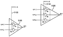
도 9a 및 9b는 본 발명의 실시예에 따른 직교-극-직교-극(CPCP) 2-분기 벡터 전력 증폭(VPA)법을 나타낸 페이저도.
도 10은 CPCP 2-분기 VPA법의 예시적인 실시예를 나타낸 블록도.
도 10a는 CPCP 2-분기 VPA법의 다른 예시적인 실시예를 나타낸 블록도.
도 11은 CPCP 2-분기 VPA법에 따른 전력 증폭에 대한 프로세스 플로우차트 실시예를 나타낸 도.
도 12는 CPCP 2-분기 VPA법을 구현하기 위한 벡터 전력 증폭기의 예시적인 실시예를 나타낸 블록도.
도 12a는 CPCP 2-분기 VPA법을 구현하기 위한 벡터 전력 증폭기의 다른 예시적인 실시예를 나타낸 블록도.
도 12b는 CPCP 2-분기 VPA법을 구현하기 위한 벡터 전력 증폭기의 다른 예시적인 실시예를 나타낸 블록도.
도 13은 CPCP 2-분기 VPA법을 구현하기 위한 벡터 전력 증폭기의 다른 예시적인 실시예를 나타낸 블록도.
도 13a는 CPCP 2-분기 VPA법을 구현하기 위한 벡터 전력 증폭기의 다른 예시적인 실시예를 나타낸 블록도.
도 14는 본 발명의 실시예에 따른 직접 직교 2-분기 벡터 전력 증폭(VPA)법을 나타낸 페이저도.
도 15는 직접 직교 2-분기 VPA법의 예시적인 실시예를 나타낸 블록도.
도 15a는 직접 직교 2-분기 VPA법의 다른 예시적인 실시예를 나타낸 블록도.
도 16은 직접 직교 2-분기 VPA법에 따른 전력 증폭에 대한 프로세스 플로우차트 실시예를 나타낸 도.
도 17은 직접 직교 2-분기 VPA법을 구현하기 위한 벡터 전력 증폭기의 예시적인 실시예를 나타낸 블록도.
도 17a는 직접 직교 2-분기 VPA법을 구현하기 위한 벡터 전력 증폭기의 다른 예시적인 실시예를 나타낸 블록도.
도 17b는 직접 직교 2-분기 VPA법을 구현하기 위한 벡터 전력 증폭기의 다른 예시적인 실시예를 나타낸 블록도.
도 18은 직접 직교 2-분기 VPA법을 구현하기 위한 벡터 전력 증폭기의 다른 예시적인 실시예를 나타낸 블록도.
도 18a는 직접 직교 2-분기 VPA법을 구현하기 위한 벡터 전력 증폭기의 다른 예시적인 실시예를 나타낸 블록도.
도 19는 직교 4-분기 VPA법에 따른 I 및 Q 전달 함수 실시예를 나타낸 프로세스 플로우차트.
도 20은 직교 4-분기 VPA법에 따른 I 및 Q 전달 함수의 예시적인 실시예를 나타낸 블록도.
도 21은 CPCP 2-분기 VPA법에 따른 I 및 Q 전달 함수 실시예를 나타낸 프로세스 플로우차트.
도 22는 CPCP 2-분기 VPA법에 따른 I 및 Q 전달 함수의 예시적인 실시예를 나타낸 블록도.
도 23은 직접 직교 2-분기 VPA법에 따른 I 및 Q 전달 함수 실시예를 나타낸 프로세스 플로우차트.
도 24는 직접 직교 2-분기 VPA법에 따른 I 및 Q 전달 함수의 예시적인 실시예를 나타낸 블록도.
도 25는 신호 페이저 표기에 대한 파형 왜곡의 영향을 나타낸 페이저도.
도 26은 본 발명의 실시예에 따른 크기-위상 변환 함수를 나타낸 도.
도 27은 본 발명의 실시예에 따른 바이어싱 회로의 예시적인 실시예를 나타낸 도.
도 28은 본 발명의 실시예에 따른 일정 포락선 신호들을 결합하는 방법을 나타낸 도.
도 29는 본 발명에 따른 벡터 전력 증폭기 출력단 실시예를 나타낸 도.
도 30은 전력 증폭기(PA) 출력단 실시예의 블록도.
도 31은 다른 전력 증폭기(PA) 출력단 실시예의 블록도.
도 32는 다른 전력 증폭기(PA) 출력단 실시예의 블록도.
도 33은 본 발명에 따른 다른 전력 증폭기(PA) 출력단 실시예의 블록도.
도 34는 본 발명에 따른 다른 전력 증폭기(PA) 출력단 실시예의 블록도.
도 35는 본 발명에 따른 다른 전력 증폭기(PA) 출력단 실시예의 블록도.
도 36은 본 발명에 따른 다른 전력 증폭기(PA) 출력단 실시예의 블록도.
도 37은 본 발명의 실시예에 따른 예시적인 출력 신호를 나타낸 도.
도 38은 예시적인 PA 실시예를 나타낸 도.
도 39는 예시적인 시변 복소 포락선 PA 출력 신호와 이에 대응하는 포락선 신호를 나타낸 도.
도 40은 PA 출력단 전류의 예시적인 타이밍도.
도 41은 예시적인 출력단 전류 제어 함수를 나타낸 도.
도 42는 다른 전력 증폭기(PA) 출력단 실시예의 블록도.
도 43은 예시적인 PA단 실시예를 나타낸 도.
도 44는 예시적인 파형 PA 출력 신호를 나타낸 도.
도 45는 전력 제어 방법을 나타낸 도.
도 46은 다른 전력 제어 방법을 나타낸 도.
도 47은 예시적인 벡터 전력 증폭기 실시예를 나타낸 도.
도 48은 본 발명의 실시예에 따른 출력단 전류 정형(shaping)을 구현하기 위한 프로세스 플로우차트.
도 49는 본 발명의 실시예에 따른 고조파 제어를 구현하기 위한 프로세스 플로우차트.
도 50은 본 발명의 실시예에 따른 전력 증폭을 구현하기 위한 프로세스 플로우차트.
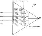
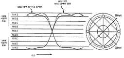
도 51a 내지 51i는 예시적인 다중 입력 단일 입력(MISO) 출력단 실시예를 나타낸 도.
도 52는 예시적인 MISO 증폭기 실시예를 나타낸 도.
도 53은 여러 가지 통신 표준에 있어서 하위 및 상위 스펙트럼 대역 상의 주파수 대역 할당을 나타낸 도.
도 54a 및 54b는 에러 보상을 위한 피드포워드 기술을 나타낸 도.
도 55는 수신기 기반 피드백 에러 정정 기술을 나타낸 도.
도 56은 디지털 제어 모듈 실시예를 나타낸 도.
도 57은 다른 디지털 제어 모듈 실시예를 나타낸 도.
도 58은 다른 디지털 제어 모듈 실시예를 나타낸 도.
도 59는 VPA 아날로그 코어 실시예를 나타낸 도.
도 60은 도 59의 VPA 아날로그 코어 실시예에 따른 출력단 실시예를 나타낸 도.
도 61은 다른 VPA 아날로그 코어 실시예를 나타낸 도.
도 62는 도 61의 VPA 아날로그 코어 실시예에 따른 출력단 실시예를 나타낸 도.
도 63은 다른 VPA 아날로그 코어 실시예를 나타낸 도.
도 64는 도 63의 VPA 아날로그 코어 실시예에 따른 출력단 실시예를 나타낸 도.
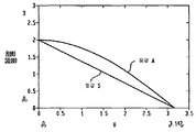
도 65는 본 발명의 실시예에 따른, 예시적인 파형을 이용한 실시간 증폭기 등급 제어를 나타낸 도.
도 66은 출력 전력 대 아웃페이징(outphasing) 각의 예시적인 플롯을 나타낸 도.
도 67은 본 발명의 실시예에 따른, 예시적인 QPSK 파형을 이용한 예시적인 전력 제어 메카니즘을 나타낸 도.
도 68은 본 발명의 실시예에 따른, 예시적인 파형을 이용한 실시간 증폭기 등급 제어를 나타낸 도.
도 69는 본 발명의 실시예에 따른, 예시적인 파형을 이용한 실시간 증폭기 등급 제어를 나타낸 도.
도 70은 본 발명의 실시예에 따른, 이론적인 VPA 출력단 효율 대 VPA 출력단 전류의 예시적인 플롯을 나타낸 도.
도 71은 본 발명의 실시예에 따른 예시적인 VPA를 나타낸 도.
도 72는 본 발명의 실시예에 따른, 전력 증폭기에서의 실시간 증폭기 등급 제어 방법을 나타낸 프로세스 플로우차트.
도 73은 예시적인 VPA 출력단을 나타낸 도.
도 74는 도 73의 VPA 출력단의 증폭기 등급 S 동작에 대한 등가회로도.
도 75는 도 73의 VPA 출력단의 증폭기 등급 A 동작에 대한 등가회로도.
도 76은 도 73의 VPA 출력단의 증폭기 등급 A 및 등급 S 동작에 대한 예시적인 크기-위상 천이 변환 함수를 나타낸 플롯도.
도 77은 도 73의 VPA 출력단의 동작의 증폭기 등급의 범위에 대응하는 크기-위상 천이 변환 함수의 스펙트럼을 나타낸 플롯도.
도 78은 분기 위상 및 진폭 에러가 있을 때에의 크기-위상 천이 변환의 수학적 유도를 나타낸 도.
본 발명은 첨부도면을 참조로 설명한다. 도면에서, 처음 나타나는 구성 요소는 통상적으로 해당 도면부호의 최좌측 숫자로 나타낸다.Embodiments of the present invention will be described with reference to the accompanying drawings. In the drawings, like reference numerals designate like or functionally similar elements. Also generally, the leftmost digit of the reference number identifies the drawing in which the relevant component is first introduced.
FIG. 1A is an exemplary diagram illustrating the generation of an exemplary time-varing complex envelope signal; FIG.
FIG. 1B is another exemplary diagram illustrating the generation of an exemplary time varying complex envelope signal; FIG.
Figure 1C illustrates generation of an exemplary time varying complex envelope signal from a sum of two or more constant envelope signals;
1D illustrates power amplification of an exemplary time varying complex envelope signal according to an embodiment of the present invention.
1e is a block diagram illustrating a vector power amplification embodiment of the present invention.
1 shows a phasor representation of a signal.
2 is a diagram illustrating a pager representation of a time-varying complex envelope signal;
Figures 3A-3C illustrate exemplary modulation for generating a time varying complex envelope signal.
FIG. 3D is an example showing a constant envelope decomposition of a time-varying envelope signal; FIG.
4 is a pager diagram illustrating an orthogonal 4-branch vector power amplification (VPA) method in accordance with an embodiment of the present invention.
5 is a block diagram illustrating an exemplary embodiment of an orthogonal 4-branch VPA method.
6 illustrates a process flow chart embodiment for power amplification according to an orthogonal 4-branch VPA method;
7A is a block diagram illustrating an exemplary embodiment of a vector power amplifier for implementing an orthogonal 4-branch VPA method.
7B is a block diagram illustrating another exemplary embodiment of a vector power amplifier for implementing an orthogonal 4-branch VPA method.
8A is a block diagram illustrating another exemplary embodiment of a vector power amplifier according to an orthogonal 4-branch VPA method.
8B is a block diagram illustrating another exemplary embodiment of a vector power amplifier according to an orthogonal 4-branch VPA method.
8C is a block diagram illustrating another exemplary embodiment of a vector power amplifier according to an orthogonal 4-branch VPA method.
8D is a block diagram illustrating another exemplary embodiment of a vector power amplifier according to an orthogonal 4-branch VPA method.
9A and 9B are pager diagrams illustrating an orthogonal-pole-to-orthogonal-pole (CPCP) two-branch vector power amplification (VPA) method in accordance with an embodiment of the present invention.
10 is a block diagram showing an exemplary embodiment of the CPCP 2-branch VPA method.
10A is a block diagram illustrating another exemplary embodiment of a CPCP two-branch VPA method.
11 illustrates a process flow chart embodiment for power amplification according to the CPCP 2-branch VPA method;
12 is a block diagram illustrating an exemplary embodiment of a vector power amplifier for implementing a CPCP two-branch VPA method;
12A is a block diagram illustrating another exemplary embodiment of a vector power amplifier for implementing the CPCP two-branch VPA method.
12B is a block diagram illustrating another exemplary embodiment of a vector power amplifier for implementing the CPCP 2-branch VPA method.
Figure 13 is a block diagram illustrating another exemplary embodiment of a vector power amplifier for implementing the CPCP two-branch VPA method.
13A is a block diagram illustrating another exemplary embodiment of a vector power amplifier for implementing the CPCP two-branch VPA method.
14 is a pager diagram illustrating a direct orthogonal 2-branch vector power amplification (VPA) method in accordance with an embodiment of the present invention.
15 is a block diagram showing an exemplary embodiment of a direct orthogonal two-branch VPA method;
15A is a block diagram illustrating another exemplary embodiment of a direct orthogonal 2-branch VPA method.
16 is a flowchart showing an embodiment of a process flow chart for power amplification according to a direct orthogonal two-branch VPA method;
17 is a block diagram illustrating an exemplary embodiment of a vector power amplifier for implementing a direct orthogonal 2-branch VPA method;
17A is a block diagram illustrating another exemplary embodiment of a vector power amplifier for implementing a direct orthogonal two-branch VPA method.
17B is a block diagram illustrating another exemplary embodiment of a vector power amplifier for implementing a direct orthogonal two-branch VPA method.
18 is a block diagram illustrating another exemplary embodiment of a vector power amplifier for implementing a direct orthogonal two-branch VPA method;
18A is a block diagram illustrating another exemplary embodiment of a vector power amplifier for implementing a direct orthogonal 2-branch VPA method.
19 is a process flow chart illustrating I and Q transfer function embodiments according to an orthogonal 4-branch VPA method.
20 is a block diagram illustrating an exemplary embodiment of an I and Q transfer function according to an orthogonal 4-branch VPA method;
21 is a process flow chart illustrating I and Q transfer function embodiments according to the CPCP two-branch VPA method.
22 is a block diagram illustrating an exemplary embodiment of I and Q transfer functions in accordance with the CPCP two-branch VPA method;
23 is a process flow chart illustrating I and Q transfer function embodiments according to a direct orthogonal 2-branch VPA method;
24 is a block diagram illustrating an exemplary embodiment of an I and Q transfer function according to a direct orthogonal 2-branch VPA method;
Figure 25 is a pager diagram showing the effect of waveform distortion on signal pager notation.
26 illustrates a magnitude-to-phase conversion function according to an embodiment of the present invention.
Figure 27 illustrates an exemplary embodiment of a biasing circuit in accordance with an embodiment of the present invention;
28 illustrates a method of combining constant envelope signals according to an embodiment of the present invention.
29 illustrates a vector power amplifier output stage embodiment according to the present invention.
30 is a block diagram of a power amplifier (PA) output stage embodiment;
31 is a block diagram of another power amplifier (PA) output stage embodiment;
32 is a block diagram of another power amplifier (PA) output stage embodiment;
33 is a block diagram of another power amplifier (PA) output stage embodiment according to the present invention;
34 is a block diagram of another power amplifier (PA) output stage embodiment in accordance with the present invention;
35 is a block diagram of another power amplifier (PA) output stage embodiment in accordance with the present invention;
Figure 36 is a block diagram of another power amplifier (PA) output stage embodiment in accordance with the present invention;
Figure 37 illustrates an exemplary output signal in accordance with an embodiment of the present invention.
38 illustrates an exemplary PA embodiment;
39 illustrates an exemplary time varying complex PA PA output signal and corresponding envelope signal;
Figure 40 is an exemplary timing diagram of PA output current.
Figure 41 illustrates an exemplary output stage current control function;
42 is a block diagram of another power amplifier (PA) output stage embodiment;
Figure 43 illustrates an exemplary PA only embodiment;
44 shows an exemplary waveform PA output signal;
45 shows a power control method;
46 is a diagram showing another power control method;
Figure 47 illustrates an exemplary vector power amplifier embodiment;
Figure 48 is a process flow chart for implementing output stage current shaping in accordance with an embodiment of the present invention.
49 is a process flow chart for implementing harmonic control according to an embodiment of the present invention;
50 is a process flow chart for implementing power amplification according to an embodiment of the present invention;
Figures 51A-51I illustrate an exemplary multiple input single input (MISO) output stage embodiment.
52 illustrates an exemplary MISO amplifier embodiment;
Figure 53 illustrates frequency band allocation on lower and higher spectral bands in various communication standards.
54A and 54B are diagrams illustrating a feedforward technique for error compensation;
55 illustrates a receiver based feedback error correction technique;
56 shows an embodiment of a digital control module;
57 illustrates another digital control module embodiment;
58 shows another digital control module embodiment;
59 illustrates a VPA analog core embodiment;
Figure 60 illustrates an output stage embodiment in accordance with the VPA analog core embodiment of Figure 59;
61 shows another VPA analog core embodiment;
Figure 62 illustrates an output stage embodiment in accordance with the VPA analog core embodiment of Figure 61;
63 illustrates another VPA analog core embodiment;
Figure 64 illustrates an output stage embodiment in accordance with the VPA analog core embodiment of Figure 63;
Figure 65 illustrates real-time amplifier grade control using an exemplary waveform, in accordance with an embodiment of the present invention.
66 is a diagram illustrating an exemplary plot of output power versus outphasing angle;
67 is a diagram illustrating an exemplary power control mechanism using an exemplary QPSK waveform, in accordance with an embodiment of the present invention.
68 is a diagram illustrating real-time amplifier grade control using an exemplary waveform, in accordance with an embodiment of the present invention.
69 illustrates real-time amplifier grade control using an exemplary waveform, in accordance with an embodiment of the present invention.
Figure 70 illustrates an exemplary plot of the theoretical VPA output stage efficiency vs. VPA output stage current, in accordance with an embodiment of the present invention.
71 illustrates an exemplary VPA in accordance with an embodiment of the present invention.
72 is a process flow chart illustrating a method for controlling a real-time amplifier rating in a power amplifier, in accordance with an embodiment of the present invention.
73 shows an exemplary VPA output stage;
74 is an equivalent circuit diagram for amplifier class S operation of the VPA output stage of FIG. 73;
75 is an equivalent circuit diagram for amplifier class A operation of the VPA output stage of FIG. 73;
76 is a plot showing an exemplary magnitude-to-phase transition conversion function for amplifier class A and class S operation of the VPA output stage of FIG. 73;
FIG. 77 is a plot showing the spectrum of a magnitude-to-phase shift conversion function corresponding to a range of amplifier ratings of the operation of the VPA output stage of FIG. 73; FIG.
78 shows a mathematical derivation of a magnitude-phase shift transformation when there is a branch phase and amplitude error;
The invention will now be described with reference to the accompanying drawings. In the drawings, the first appearing component is typically indicated by the leftmost digit of the reference numeral.
목차Contents
1. 소개1. Introduction
1.1. 시변 복소 포락선 입력 신호의 예시적인 생성1.1. An exemplary generation of a time-varying complex envelope input signal
1.2. 일정 포락선 신호로부터의 시변 복소 포락선 신호의 예시적인 생성1.2. An exemplary generation of a time-varying complex envelope signal from a constant envelope signal
1.3. 벡터 전력 증폭 개관1.3. Vector power amplification overview
2. 일반적인 수학적 개관2. General mathematical overview
2.1. 페이저 신호 표기2.1. Phaser Signals
2.2. 시변 복소 포락선 신호2.2. Time-varying complex envelope signal
2.3. 시변 포락선 신호의 일정 포락선 분해2.3. Constant envelope decomposition of time-varying envelope signal
3. 벡터 전력 증폭(VPA) 방법 및 시스템3. Vector Power Amplification (VPA) Method and System
3.1. 직교 4-분기 벡터 전력 증폭기3.1. Orthogonal 4-branch vector power amplifier
3.2. 직교-극-직교-극 (CPCP) 2-분기 벡터 전력 증폭기3.2. Quadrature-pole-to-quadrature-pole (CPCP) two-branch vector power amplifier
3.3. 직접 직교 2-분기 벡터 전력 증폭기3.3. Direct Orthogonal 2-Branch Vector Power Amplifier
3.4. I 및 Q 데이터-벡터 변조기 전달 함수3.4. I and Q data-vector modulator transfer functions
3.4.1. 직교 4-분기 VPA 전달 함수3.4.1. Orthogonal 4-branch VPA transfer function
3.4.2. CPCP 2-분기 VPA 전달 함수3.4.2. CPCP 2-branch VPA transfer function
3.4.3. 직접 직교 2-분기 VPA 전달 함수3.4.3. Direct orthogonal 2-branch VPA transfer function
3.4.4. 크기-위상 천이 변환3.4.4. Size-to-phase shift conversion
3.4.4.1. 정현파 신호에 대한 크기-위상 천이 변환3.4.4.1. The magnitude-to-phase shift conversion for the sinusoidal signal
3.4.4.2. 구형파 신호에 대한 크기-위상 천이 변환3.4.4.2. The magnitude-to-phase shift transformation
3.4.5. 파형 왜곡 보상3.4.5. Waveform distortion compensation
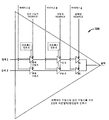
3.5. 출력단3.5. Output stage
3.5.1. 출력단 실시예3.5.1. Output stage embodiment
3.5.2. 출력단 전류 정형3.5.2. Output stage current shaping
3.5.3. 출력단 보호3.5.3. Output stage protection
3.6. 고조파 제어3.6. Harmonic control
3.7. 전력 제어3.7. Power control
3.8. 예시적인 벡터 전력 증폭기 실시예3.8. Exemplary Vector Power Amplifier Embodiments
4. 추가 예시적인 실시예 및 구현4. Additional illustrative embodiments and implementations
4.1. 개관4.1. survey
4.1.1. 출력 전력 및 전력 효율의 제어4.1.1. Control of output power and power efficiency
4.1.2. 에러 보상 및/또는 보정4.1.2. Error compensation and / or correction
4.1.3. 다중대역 다중모드 동작4.1.3. Multi-band multimode operation
4.2. 디지털 제어 모듈4.2. Digital control module
4.3. VPA 아날로그 코어4.3. VPA analog core
4.3.1. VPA 아날로그 코어 구현 A4.3.1. VPA Analog Core Implementation A
4.3.2. VPA 아날로그 코어 구현 B4.3.2. VPA analog core implementation B
4.3.3. VPA 아날로그 코어 구현 C4.3.3. VPA analog core implementation C
5. VPA 출력단의 실시간 증폭기 등급 제어5. Real-time amplifier grade control of VPA output stage
6. 요약6. Summary
7. 결론
7. Conclusion
소개Introduce
본 명세서에서는 벡터 결합 전력 증폭 방법, 장치 및 시스템이 개시된다.A vector coupled power amplification method, apparatus and system are disclosed herein.
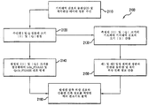
벡터 결합 전력 증폭은 선형성과 전력 효율을 동시에 최적화하는 방식이다. 일반적으로 말하여, 도 50의 플로우차트(502)를 참조로 설명하면, 단계(504)에서 진폭과 위상이 변하는 시변 복소 포락선 입력 신호는 일정 포락선 성분 신호들로 분해된다. 단계(506)에서 일정 포락선 성분 신호들은 증폭되고, 단계(508)에서 합산되어 입력 복소 포락선 신호의 증폭 신호를 생성한다. 실질적으로 일정한 포락선 신호는 비선형 왜곡이 거의 없이 증폭될 수 있기 때문에 일정 포락선 신호들을 합산한 결과도 비선형 왜곡이 거의 없이 최적 효율을 제공한다.Vector coupling power amplification is a method of simultaneously optimizing linearity and power efficiency. Generally speaking, with reference to
따라서 벡터 결합 전력 증폭에 의해서 비선형 전력 증폭기라도 비선형 왜곡 레벨을 최소화하면서 복소 신호를 효율적으로 증폭하는데 사용될 수 있다.Therefore, even a nonlinear power amplifier can be used to efficiently amplify a complex signal while minimizing the nonlinear distortion level by vector coupling power amplification.
편의상 제한없이 본 명세서에서는 본 발명의 방법 및 시스템은 때로는 벡터 전력 증폭(VPA) 방법 및 시스템이라고 한다.For convenience, the method and system of the present invention is sometimes referred to herein as a vector power amplification (VPA) method and system.
이제 본 발명의 실시예들에 따른 VPA 방법 및 시스템에 대해서 자세히 설명하기로 한다. 명확하게 하기 위하여 먼저 특정 용어들에 대해서 정의한다. 이 절에서 기술된 정의는 단순히 편의상 제공하는 것이며 제한적인 것이 아니다. 이들 용어들의 의미는 본 발명의 교시에 따라 당업자에게 명백하게 될 것이다. 이들 용어는 명세서 전체에서 추가적인 세부사항을 가지고 설명될 수 있다.The VPA method and system according to embodiments of the present invention will now be described in detail. For clarity, we first define certain terms. The definitions described in this section are provided for convenience only and are not restrictive. The meaning of these terms will be apparent to those skilled in the art in accordance with the teachings of the present invention. These terms may be described with additional details throughout the specification.
여기서 사용되는 용어 "신호 포락선"은 신호가 시간 영역에서 변동할 때에 포함되는 진폭 경계를 말한다. 직교 변조 신호는 r(t)=i(t)·cos(ωc·t)+q(t)·sin(ωc·t)로 표현될 수 있다. 이 식에서 i(t)와 q(t)는 신호 포락선(
여기서 사용되는 용어 "일정 포락선 신호"는 
여기서 사용되는 용어 "시변 포락선 신호"는 시변 신호 포락선을 가진 신호를 말한다. 시변 포락선 신호는 동위상 및 직각 위상 신호의 관점에서 시변값을 가진 
여기서 사용된 용어 "위상 천이(phase shifting)"는 시변 또는 일정 포락선 신호의 위상 성분이 기준 위상에 대해 지상(delaying) 또는 진상(advancing)하는 것을 말한다.As used herein, the term "phase shifting" refers to the phase component of a time-varying or constant envelope signal delaying or advancing relative to a reference phase.
1.1) 시변 복소 포락선 입력 신호의 예시적인 생성1.1) An exemplary generation of a time-varying complex envelope input signal
도 1a 및 도 1b는 시변 포락선 및 위상 복소 입력 신호의 생성을 나타낸 예시도이다. 도 1a에서, 시변 포락선 반송파 신호(104, 106)는 위상 제어기(110)에 입력된다. 위상 제어기(110)는 신호(104, 106)의 위상 성분을 조작한다. 즉, 위상 제어기(110)는 신호(104, 106)의 위상을 천이시킬 수 있다. 따라서 도출된 신호(108, 112)는 신호(104, 106)에 대해 위상이 천이될 수 있다. 도 1a의 예에서 위상 제어기(110)는 신호(108, 112)로부터 알 수 있듯이 시상수(t0)에서 신호(104, 106)의 위상을 반전(180도 위상 천이)시킨다. 신호(108, 112)는 시변 복소 반송파 신호를 나타낸다. 신호(108, 112)는 시변 포락선 및 위상 성분 둘 다를 갖고 있다. 신호(108, 112)는 합쳐져서 신호(114)가 된다. 신호(114)도 시변 복소 신호를 나타낸다. 신호(114)는 본 발명의 VPA 실시예에서의 예시적인 입력 신호(예컨대 도 50의 단계(504)에서의 예시적인 입력)일 수 있다.Figures 1A and 1B illustrate generation of time-varying envelope and phase complex input signals. In FIG. 1A, time-varying envelope carrier signals 104 and 106 are input to a
시변 복소 신호는 또한 도 1b에 도시된 바와 같이 생성될 수 있다. 도 1b에서 신호(116, 118)는 기저대역 신호를 나타낸다. 예컨대 신호(116, 118)는 신호의 동위상(I) 및 직각위상(Q) 기저대역 성분일 수 있다. 도 1b의 예에서 신호(116, 118)는 +1에서 -1로 전이함에 따라 영교차(zero crossing)한다. 신호(116, 118)에는 신호(120) 또는 90도 위상 천이된 신호(120)가 곱해진다. 신호(116)에는 0도 천이된 버전의 신호(120)가 곱해진다. 신호(118)에는 90도 천이된 버전의 신호(120)가 곱해진다. 이렇게 해서 도출된 신호(122, 124)는 시변 복소 반송파 신호를 나타낸다. 여기서 신호(122, 124)는 신호(116, 118)의 시변 진폭에 따라 변하는 포락선을 갖고 있음에 유의한다. 더욱이 신호(122, 124)는 모두 신호(116, 118)의 영교차에서 위상 반전을 겪는다. 신호(122, 124)는 합산되어 신호(126)가 된다. 신호(126)는 시변 복소 신호를 나타낸다. 신호(126)는 본 발명의 VPA 실시예에서 예시적인 입력 신호를 나타낼 수 있다. 게다가 신호(116, 118)는 본 발명의 VPA 실시예에서 예시적인 입력 신호들을 나타낼 수 있다.The time varying complex signal can also be generated as shown in FIG. In FIG. 1B, signals 116 and 118 represent a baseband signal. For example, signals 116 and 118 may be in-phase (I) and quadrature-phase (Q) baseband components of the signal. In the example of FIG. 1B, the
1.2) 일정 포락선 신호로부터의 시변 복소 포락선 신호의 예시적인 생성1.2) Exemplary generation of a time-varying complex envelope signal from a constant envelope signal
이 절에서의 설명은 일반적으로 도 50에서 단계(508)의 동작에 관한 것이다. 도 1c는 2 또는 그 이상의 실질적으로 일정한 포락선 신호의 합으로부터의 시변 복소 신호의 생성의 3가지 예를 나타낸다. 그러나 당업자라면 본 발명의 교시에 따라서 도 1c의 예에 나타난 개념은 마찬가지로 2보다 많은 일정 포락선 신호의 경우에 확장될 수 있음을 잘 알 것이다.The description in this section generally refers to the operation of step 508 in FIG. Figure 1C shows three examples of the generation of a time-varying complex signal from a sum of two or more substantially constant envelope signals. However, those skilled in the art will appreciate that in accordance with the teachings of the present invention, the concept shown in the example of FIG. 1C can likewise be extended in the case of more than two constant envelope signals.
도 1c의 예 1에서 일정 포락선 신호(132. 134)는 위상 제어기(130)에 입력된다. 위상 제어기(130)는 신호(132, 134)의 위상 성분을 조작하여 각각 신호(136, 138)를 생성한다. 신호(136, 138)는 실질적으로 일정한 포락선 신호를 나타내며, 합산되어 신호(140)를 생성한다. 도 1c의 예 1과 관련된 페이저 표기는 신호(136, 138)를 각각 페이저(P136, P138)로서 나타낸다. 신호(140)는 페이저(P140)로서 나타낸다. 예 1에서 P136과 P138은 페이저 표기의 실축에 맞추어지도록 가정된 기준 신호에 대해 각도(φ1)만큼 대칭적으로 위상 천이되어 있다. 이에 대응하여 시간 영역 신호(136, 138)는 기준 신호에 대해 양은 동일하나 방향은 반대로 위상이 천이되어 있다. 따라서 P136과 P138의 합인 P140은 기준 신호와 위상이 같다.The
도 1c의 예 2에서 실질적으로 일정한 포락선 신호(132, 134)는 위상 제어기(130)에 입력된다. 위상 제어기(130)는 신호(132, 134)의 위상 성분을 조작하여 각각 신호(142, 144)를 생성한다. 신호(142, 144)는 실질적으로 일정한 포락선 신호를 나타내며, 합산되어 신호(150)를 생성한다. 예 2와 관련된 페이저 표기는 신호(142, 144)를 각각 페이저(P142, P144)로서 나타낸다. 신호(150)는 페이저(P150)로서 나타낸다. 예 2에서 P142과 P144는 기준 신호에 대해 대칭적으로 위상 천이되어 있다. 따라서 P140과 마찬가지로 P150도 기준 신호와 위상이 같다. 그러나 P142과 P144는 기준 신호에 대해 소정 각도(φ2≠φ1)만큼 위상 천이된다. 그 결과, P150은 예 1의 P140과는 크기가 다르다. 시간 영역 표기에서는 신호(140, 150)는 동위상이지만 진폭은 서로 다르다.The substantially constant envelope signals 132 and 134 in Example 2 of Figure 1C are input to the
도 1c의 예 3에서 실질적으로 일정한 포락선 신호(132, 134)는 위상 제어기(130)에 입력된다. 위상 제어기(130)는 신호(132, 134)의 위상 성분을 조작하여 각각 신호(146, 148)를 생성한다. 신호(146, 148)는 실질적으로 일정한 포락선 신호를 나타내며, 합산되어 신호(160)를 생성한다. 예 3과 관련된 페이저 표기는 신호(146, 148)를 각각 페이저(P146, P148)로서 나타낸다. 신호(160)는 페이저(P160)로서 나타낸다. 예 3에서 P146은 기준 신호에 대해 각도(φ3)만큼 위상 천이되어 있다. P148은 기준 신호에 대해 각도(φ4)만큼 위상 천이되어 있다. φ3과 φ4는 같을 수도 같지 않을 수도 있다. 따라서 P146과 P148의 합인 P160은 기준 신호와 더 이상 동위상이 아니다. P160은 기준 신호에 대해 각도(Θ)만큼 위상 천이된다. 마찬가지로 P160은 예 1과 2의 P140과 P150에 대해 Θ만큼 위상 천이된다. P160은 예 3에 도시된 바와 같이 P140에 대해 진폭이 변화될 수도 있다.The substantially constant envelope signals 132 and 134 in Example 3 of Figure 1C are input to the
요약하면, 도 1c의 예들은 2 또는 그 이상의 실질적으로 일정한 포락선 신호의 합에 의해 시변 진폭 신호가 얻어질 수 있다는 것(예 1)을 보여준다. 더욱이 2 또는 그 이상의 실질적으로 일정한 포락선 신호를 반대 방향에서 동일하게 천이시킴으로써 위상 변화없이 진폭만 변화시킬 수 있다(예 2). 2 또는 그 이상의 일정한 포락선 성분 신호를 동일 방향에서 동일하게 천이시킴으로써 시변 신호는 진폭 변화없이 위상만 변화시킬 수 있다. 2 또는 그 이상의 실질적으로 일정한 포락선 신호를 이용하여 임의의 시변 진폭 및 위상 신호를 생성할 수 있다(예 3).In summary, the examples of FIG. 1C show that a time-varying amplitude signal can be obtained (Example 1) by the sum of two or more substantially constant envelope signals. Furthermore, by shifting two or more substantially constant envelope signals in the same direction in the opposite direction, only the amplitude can be changed without changing the phase (Example 2). By shifting two or more constant envelope component signals in the same direction in the same direction, the time-varying signal can only change its phase without changing the amplitude. Two or more substantially constant envelope signals may be used to generate any time-varying amplitude and phase signal (Example 3).
도 1c의 예에서의 신호들은 단지 설명을 위해 정현파형으로 도시한 점에 유의한다. 당업자라면 본 발명의 교시에 따라 임의 형태의 파형이 이용될 수 있음을 잘 알 것이다. 또한 도 1c의 예는 단지 설명을 위해 제공된 것이며 본 발명의 특정 실시예에 해당될 수도 있고 해당되지 않을 수도 있음에 유의한다.Note that the signals in the example of FIG. 1C are shown as sinusoidal for illustration purposes only. It will be appreciated by those skilled in the art that any form of waveform may be used in accordance with the teachings of the present invention. It should also be noted that the example of Figure 1c is provided for illustrative purposes only and may or may not correspond to a particular embodiment of the present invention.
1.3) 벡터 전력 증폭 개관1.3) Vector power amplification overview
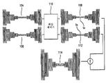
이제 벡터 전력 증폭에 대해 자세히 개관한다. 도 1d는 예시적인 시변 복소 입력 신호(172)의 전력 증폭을 나타낸다. 도 1a와 1b에 도시된 신호(114, 126)는 신호(172)의 예일 수 있다. 더욱이 신호(172)는 104와 106(도 1a), 108과 112(도 1a), 116과 118(도 1b), 및 122와 124(도 1b)와 같은 2 또는 그 이상의 성분 신호에 의해 생성되거나 이 신호들로 구성될 수 있다.We now have a closer look at vector power amplification. FIG. 1D shows power amplification of an exemplary time varying
도 1d의 예에서 VPA(170)는 본 발명에 따른 VPA 시스템 실시예를 나타낸다. VPA(170)는 신호(172)를 증폭하여 증폭 출력 신호(178)를 생성한다. 출력 신호(178)는 왜곡을 최소화하면서 효율적으로 증폭된다.In the example of FIG. 1D,
도 1d의 예에서 신호(172, 178)는 각각 전압 신호(Vin(t), Vout(t)))를 나타낸다. 임의 시각에서 도 1d의 예에서 Vin(t)와 Vout(t)는 Vout(t)=KeVin(tat')의 관계를 갖는다. 여기서, K는 스케일 팩터이고 t'는 VPA 시스템에서 있을 수 있는 시간 지연을 나타낸다. 전력 표시로는 
도 1d에 도시된 바와 같이 시변 복소 신호의 선형적(또는 실질적으로 선형적) 전력 증폭은 도 1e에 도시된 본 발명의 실시예에 따라 이루어진다.The linear (or substantially linear) power amplification of the time-varying complex signal as shown in Fig. 1d is performed according to the embodiment of the invention shown in Fig. 1e.
도 1e는 본 발명의 실시예에 따른 벡터 전력 증폭 실시예를 개념적으로 나타낸 예시적인 블록도이다. 도 1e에서 입력 신호(172)는 시변 복소 신호를 나타낸다. 예컨대 입력 신호(172)는 도 1a 및 1b에 도시된 바와 같이 생성될 수 있다. 실시예에서 신호(172)는 디지털 또는 아날로그 신호일 수 있다. 더욱이, 신호(172)는 기저대역 또는 반송파 방식 신호일 수 있다.1E is an exemplary block diagram conceptually illustrating a vector power amplification embodiment according to an embodiment of the present invention. 1E, the
도 1e를 참조로 설명하면, 본 발명의 실시예에 따라 입력 신호(172) 또는 그 등가 신호는 VPA(182)에 입력된다. 도 1e의 실시예에서 VPA(182)는 상태 머신(184)과 아날로그 회로(186)를 포함한다. 상태 머신(184)은 디지털 및/또는 아날로그 성분을 포함할 수 있다. 아날로그 회로(186)는 아날로그 성분을 포함한다. VPA(182)는 입력 신호(172)를 처리하여 도 1e에 도시된 바와 같이 2 또는 그 이상의 신호(188-{1,...,n})를 생성한다. 도 1c에서 신호(136, 138, 142, 144, 146, 148)에 대해서 설명한 바와 같이, 신호(188-{1,...,n})는 서로 다른 주기에 걸쳐 서로에 대해 위상 천이될 수도 있고 천이되지 않을 수도 있다. 더욱이 VPA(182)는 신호(188-{1,...,n})의 합이 신호(194)가 되도록 신호(188-{1,...,n})를 생성하며, 이 신호(194)는 특정 실시예에서 신호(172)가 증폭된 것일 수 있다.Referring to FIG. 1E, an
계속해서 도 1e를 참조로 설명하면, 신호(188-{1,...,n})는 실질적으로 일정한 포락선 신호이다. 따라서 이전 단락에서의 설명은 도 50의 단계(504)에 해당한다.Continuing with reference to FIG. 1e, the signal 188- {1, ..., n} is a substantially constant envelope signal. Therefore, the description in the previous paragraph corresponds to step 504 in FIG.
도 50의 단계(506)에 일반적으로 해당하는 도 1e의 예에서 일정 포락선 신호(188-{1,...,n})는 해당 전력 증폭기(PA)(190-{1,...,n})에 의해 각각 독립적으로 증폭되어 증폭 신호(192-{1,...,n})를 생성한다. 실시예에서 PA(190-{1,...,n})는 실질적으로 똑 같은 각자의 일정 포락선 신호(188-{1,...,n})를 증폭한다. 증폭 신호(192-{1,...,n})는 실질적으로 일정한 포락선 신호이며, 단계(508)에서 합산되어 출력 신호(194)를 생성한다. 출력 신호(194)는 입력 신호(172)가 선형적으로(또는 실질적으로 선형적으로) 증폭된 것일 수 있음에 유의한다. 출력 신호(194)는 여기서 설명하는 바와 같이 입력 신호(172)를 주파수 상향 변환한 것일 수도 있다.
1, ..., n} in the example of FIG. 1E, which corresponds generally to step 506 of FIG. 50, the corresponding envelope signal 188- { n} to generate amplified signals 192 - {1, ..., n}. In the embodiment, the PA 190 - {1, ..., n} amplifies substantially the same constant envelope signal 188 - {1, ..., n}. The amplified signal 192- {1, ..., n} is a substantially constant envelope signal and is summed in step 508 to produce an
일반적인 수학적 개관General mathematical overview
2.1) 페이저 신호 표기2.1) Phaser Signals
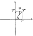
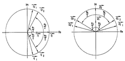
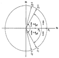
도 1은 신호(r(t))의 페이저 표기(![]()
![]()
![]()
![]()
![]()
![]()
계속해서 도 1을 참조로 설명하면, 페이저(![]()
![]()
![]()
![]()
![]()
![]()
![]()
![]()
![]()
![]()
![]()
![]()
![]()
![]()
![]()
![]()

도 1의 예에서 R(t)는 특정 순간에서 나타낸 것임에 유의한다.Note that R (t) in the example of Fig. 1 is shown at a specific moment.
2.2) 시변 복소 포락선 신호2.2) Time-varying complex envelope signal
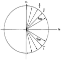
도 2는 두 개의 서로 다른 순간(t1, t2)에서의 신호(r(t))의 페이저 표기를 나타낸다. 신호의 포락선의 크기와 그 상대적인 위상 천이를 나타내는 이 페이저의 크기는 모두 시각 t1에서 시각 t2로 변한다는 것에 유의한다. 도 2에서는 이것은 페이저 ![]()
![]()
![]()
![]()
더욱이, 도 2로부터 신호(r(t))의 실수 및 허수 페이저 성분은 진폭이 시간에 따라 변한다는 것을 유의한다. 따라서 그 대응하는 시간 영역 신호도 시변 포락선을 갖는다.Furthermore, it should be noted from Figure 2 that the real and imaginary phasor components of the signal r (t) vary in amplitude with time. Therefore, the corresponding time-domain signal also has a time-varying envelope.
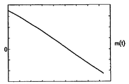
도 3a 내지 3c는 시변 복소 포락선 신호를 발생하는 예시적인 변조를 나타낸다. 도 3a는 신호(m(t))를 나타낸 것이다. 도 3b는 반송파 신호(c(t))의 일부를 나타낸 것이다. 도 3c는 신호들(m(t), c(t))을 곱하여 생성한 신호(r(t))를 나타낸 것이다.3A-3C illustrate exemplary modulation for generating a time varying complex envelope signal. Fig. 3A shows the signal m (t). FIG. 3B shows a part of the carrier signal c (t). 3C shows a signal r (t) generated by multiplying the signals m (t), c (t).
도 3a의 예에서 신호(m(t))는 시변 크기 신호이다. 더욱이 m(t)는 영교차된다. 도 3b의 예에서 반송파 신호(c(t))는 통상적으로는 신호(m(t)) 주파수보다 높은 특정 반송파 주파수로 진동한다.In the example of Fig. 3A, the signal m (t) is a time-varying magnitude signal. Furthermore, m (t) is zero crossed. In the example of Fig. 3b, the carrier signal c (t) oscillates at a particular carrier frequency, which is typically higher than the signal m (t).
도 3c로부터, 도출된 신호(r(t))는 시변 포락선을 갖고 있음을 알 수 있다. 더욱이 도 3c로부터 r(t)는 변조 신호(m(t))가 영교차하는 순간에 위상이 반전됨을 알 수 있다. 포락선과 위상이 일정하지 않으면 r(t)는 시변 복소 포락선 신호라고 한다.From FIG. 3C, it can be seen that the derived signal r (t) has a time-varying envelope. Furthermore, it can be seen from Fig. 3c that r (t) is inverted in phase at the moment when the modulated signal m (t) crosses zero. If the envelope and phase are not constant, r (t) is called the time-varying complex envelope signal.
2.3) 시변 포락선 신호의 일정 포락선 분해2.3) Constant envelope decomposition of time-varying envelope signal
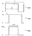
시변 크기 및 위상의 페이저는 기준 페이저에 대해 적당히 특정된 위상 천이를 갖는 2 또는 그 이상의 일정 크기 페이저의 합에 의해 얻을 수 있다.The time-varying magnitude and phasor of phase can be obtained by the sum of two or more constant-sized phasors with appropriately specified phase transitions for the reference phasor.
도 3d는 예시적인 시변 포락선 및 위상 신호(S(t))를 나타낸 것이다. 설명을 쉽게 하기 위하여 신호(S(t))는 최대 포락선 크기(A)를 가진 정현파 신호라고 가정한다. 도 3d는 두 개의 일정 포락선 신호(S1(t), S2(t))의 합에 의해 임의의 순간에 신호(S(t))가 어떻게 얻어질 수 있는가의 예를 더 보여준다. 일반적으로 S1(t)=A1sin((ωt+φ1(t))이고 S2(t)=A2sin((ωt+φ2(t))이다.Figure 3d shows an exemplary time-varying envelope and phase signal S (t). For ease of explanation, it is assumed that the signal S (t) is a sinusoidal signal having a maximum envelope size (A). FIG. 3D further shows an example of how the signal S (t) can be obtained at any instant by the sum of the two constant envelope signals S 1 (t), S 2 (t). In general, S 1 (t) = A 1 sin ((ωt + φ 1 (t)) and S 2 (t) = A 2 sin (ωt + φ 2 (t)).
설명 목적상 도 3d에는 신호 S(t)에 대해 S1(t)와 S2(t)를 적당히 조정하여 S(t)=K(S1(t)+S2(t))(여기서, K는 상수)가 되도록 신호 S1(t) 및 S2(t)가 어떻게 합산될 수 있는지를 보여주는 3개의 그림이 제공된다. 즉, 신호 S(t)는 임의 순간에 2 또는 그 이상의 신호로 분해될 수 있다. 도 3d로부터 주기 T1에서는 S1(t)와 S2(t)는 신호 S(t)에 대해 동위상이며, 따라서 합산되어 신호 S(t)의 최대 포락선 크기 A가 된다. 그러나 주기 T3에서는 신호 S1(t)와 S2(t)는 서로에 대해 위상이 180도 어긋나며, 따라서 합산되어 신호 S(t)의 최소 포락선 크기가 된다.(T) = K (S 1 (t) + S 2 (t)) where S 1 (t) and S 2 (t) are appropriately adjusted for signal S K is a picture showing how the three constants) so that the signal S 1 (t) and S 2 (t) is what may be summed is provided. That is, the signal S (t) can be decomposed into two or more signals at any moment. From FIG. 3D, S 1 (t) and S 2 (t) are in phase with respect to signal S (t) in period T 1 and are summed to become maximum envelope size A of signal S (t). However, in the period T 3 , the signals S 1 (t) and S 2 (t) are 180 degrees out of phase with respect to each other and are thus summed to the minimum envelope size of the signal S (t).
도 3d의 예는 정현파 신호의 경우를 설명한 것이다. 그러나 당업자라면 푸리에 급수 또는 푸리에 변환으로 나타낼 수 있는 반송파 신호를 변조하는 임의의 시변 포락선도 마찬가지로 2 또는 그 이상의 실질적으로 일정한 포락선 신호로 분해될 수 있음을 잘 알 것이다. 따라서 복수의 실질적으로 일정한 포락선 신호의 위상을 조정함으로써 임의의 시변 복소 포락선 신호가 생성될 수 있다.
The example of FIG. 3D is a case of a sinusoidal signal. However, those skilled in the art will appreciate that any time-varying envelope modulating a carrier signal that may be represented by a Fourier series or Fourier transform can likewise be decomposed into two or more substantially constant envelope signals. Thus, any time-varying complex envelope signal can be generated by adjusting the phase of a plurality of substantially constant envelope signals.
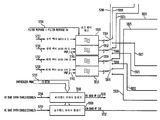
벡터 전력 증폭 방법 및 시스템Vector power amplification method and system
본 발명의 실시예에 따른 벡터 전력 증폭 방법 및 시스템은 임의의 시변 포락선 신호를 2 또는 그 이상의 실질적으로 일정한 포락선 성분 신호로 분해하거나, 그와 같은 성분 신호를 수신 또는 생성하고, 그 성분 신호를 증폭한 다음에 증폭된 신호를 합산하여 시변 복소 포락선 신호를 증폭시키는 능력에 의존한다.A vector power amplification method and system according to embodiments of the present invention decomposes any time-varying envelope signal into two or more substantially constant envelope component signals, or receives or generates such component signals, and amplifies And then the ability to amplify the time-varying complex envelope signal by summing the amplified signals.
3.1 내지 3.3 절에서는 4-분기 및 2-분기 실시예를 포함하여 본 발명의 벡터 전력 증폭(VPA) 실시예가 제공된다. 하기 설명에서는 먼저 실시예의 기본 개념의 수학적 유도를 이용하여 각 VPA 실시예를 개념적으로 제시한다. 그 후 VPA 실시예의 동작 방법의 실시예가 제시되고 나서 VPA 실시예의 각종 시스템 레벨 실시예가 제시된다.Section 3.1-3.3 provides a vector power amplification (VPA) embodiment of the present invention, including a 4-branch and a 2-branch embodiment. In the following description, each VPA embodiment is conceptually presented using the mathematical induction of the basic concept of the embodiment. An embodiment of the method of operation of the VPA embodiment is then presented, and various system level embodiments of the VPA embodiment are presented.
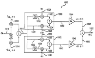
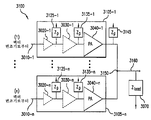
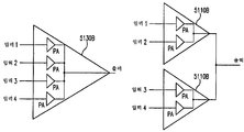
3.4 절에서는 본 발명의 실시예에 따른 제어 모듈의 여러 가지 실시예를 제시한다. 본 발명의 실시예에 따른 제어 모듈은 본 발명의 특정 VPA 실시예를 구현하는데 이용될 수 있다. 일부 실시예에서 제어 모듈은 VPA 실시예의 입력단과 VPA 실시예의 후속 벡터 변조단 사이의 중간 매개이다.Section 3.4 presents various embodiments of the control module according to an embodiment of the present invention. A control module according to an embodiment of the present invention may be used to implement a particular VPA embodiment of the present invention. In some embodiments, the control module is an intermediate between the input of the VPA embodiment and the subsequent vector modulation stage of the VPA embodiment.
3.5 절은 본 발명의 실시예에 따른 VPA 출력단 실시예에 대해서 설명한다. 출력단 실시예는 VPA 실시예의 출력 신호를 생성하는 것에 관한 것이다.Section 3.5 describes a VPA output stage embodiment according to an embodiment of the present invention. The output stage embodiment relates to generating the output signal of the VPA embodiment.
3.6 절은 본 발명의 실시예에 따른 고조파 제어에 관한 것이다. 고조파 제어는 본 발명의 특정 실시예에서 VPA 실시예의 고조파의 실수부 전력과 허수부 전력을 조작하여 출력에서의 기본 주파수에 나타나는 전력을 증가시키도록 구현될 수 있다.Section 3.6 relates to harmonic control according to an embodiment of the present invention. Harmonic control may be implemented to increase the power appearing at the fundamental frequency at the output by manipulating the real and imaginary power of the harmonic of the VPA embodiment in certain embodiments of the invention.
3.7 절은 본 발명의 실시예에 따른 전력 제어에 관한 것이다. 전력 제어는 본 발명의 VPA 실시예가 채용될 수 있는 응용의 전력 레벨 요건을 만족시키기 위해 본 발명의 특정 실시예에서 구현될 수 있다.Section 3.7 deals with power control in accordance with embodiments of the present invention. Power control may be implemented in certain embodiments of the present invention to meet power level requirements of applications in which the VPA embodiment of the present invention may be employed.
3.1. 직교 4-분기 벡터 전력 증폭기3.1. Orthogonal 4-branch vector power amplifier
여기서는 제한없이 설명을 쉽게하기 위해 직교 4-분기 VPA 실시예라 불리는 본 발명의 일 실시예에 따라서 시변 복소 포락선 신호는 4개의 실질적으로 일정한 포락선 성분 신호로 분해된다. 성분 신호는 개별적으로 똑 같이 또는 거의 똑 같이 증폭된 다음에 합산되어 원래의 시변 복소 포락선 신호의 증폭 신호를 구성한다.For ease of explanation, without limitation, the time-varying complex envelope signal is decomposed into four substantially constant envelope component signals according to an embodiment of the present invention, referred to as an orthogonal 4-branch VPA embodiment. The component signals are amplified separately or nearly equally and then summed together to form an amplified signal of the original time varying complex envelope signal.
이 실시예에서는 설명 목적상 제한없이 4 분기가 채용됨에 유의한다. 본 발명의 범위는 다른 분기 수의 이용을 포함하며, 그와 같은 변경의 구현은 본 발명의 교시에 따라 당업자에게 명백할 것이다.Note that in this embodiment, the fourth quarter is adopted without limitation for the purpose of explanation. The scope of the invention includes the use of other numbers of branches, and the implementation of such modifications will be apparent to those skilled in the art in accordance with the teachings of the present invention.
일 실시예에서 먼저 시변 복소 포락선 신호는 그 동위상 및 직각위상 벡터 성분으로 분해된다. 페이저 표기에서 동위상 및 직각위상 벡터 성분은 각각 신호의 실수부와 허수부 페이저에 해당한다.In one embodiment, the time-varying complex envelope signal is first decomposed into its in-phase and quadrature vector components. In phasor notation, the in-phase and quadrature vector components correspond to the real part of the signal and the imaginary part phasor, respectively.
전술한 바와 같이, 신호의 동위상 및 직각위상 벡터 성분의 크기는 그 신호의 크기에 비례하여 변하며, 따라서 그 신호가 시변 포락선 신호라면 일정 포락선이 아니다. 따라서 4 분기 VPA 실시예는 신호의 동위상 및 직각위상 벡터 성분 각각을 4개의 실질적으로 일정한 포락선 성분(즉, 동위상 신호 성분을 위해 2개, 직각위상 신호 성분을 위해 2개)으로 더 분해한다. 이 개념은 페이저 신호 표기를 이용하여 도 4에 나타나 있다.As described above, the magnitudes of the in-phase and quadrature-phase vector components of the signal vary in proportion to the magnitude of the signal, and thus if the signal is a time-varying envelope signal, it is not a constant envelope. Thus, the quad-quarter VPA embodiment further decomposes each of the in-phase and quadrature vector components of the signal into four substantially constant envelope components (i.e., two for the in-phase signal component and two for the quadrature signal component) . This concept is illustrated in FIG. 4 using phasor signal notation.
도 4의 예에서, 페이저 ![]()
![]()
![]()
![]()
![]()
![]()
![]()
![]()
계속해서 도 4를 참조로 설명하면, 순간 t1에서 페이저 ![]()
![]()
![]()
![]()

![]()
![]()

![]()
![]()
![]()
![]()
![]()
![]()
![]()
![]()
![]()
![]()
페이저 ![]()
![]()
![]()
![]()

![]()
![]()
![]()
![]()
![]()

![]()
![]()
![]()
![]()
![]()
![]()
![]()
![]()
![]()
![]()
![]()
일례로서 도 4에 도시된 경우에 도 4에서 ![]()
![]()
![]()
![]()
![]()
![]()
![]()
![]()

여기서, I1과 I2는 각각 페이저 ![]()
![]()
![]()
![]()
상기 설명된 개념은 마찬가지로 도 4에 도시된 신호 r(t)의 허수부 페이저, 즉 직각위상 성분에 적용될 수 있다. 따라서 임의의 시각 t에서 신호 r(t)의 허수부 페이저 ![]()
![]()
![]()
![]()
![]()
![]()
![]()
![]()
![]()
![]()
![]()
![]()
![]()
![]()
![]()
![]()
![]()
![]()
![]()
![]()
상기 설명으로부터 페이저 표기에서 가변 크기와 위상의 임의 페이저 ![]()
![]()

여기서, IU, IL, QU 및 QL은 각각 페이저 
![]()
![]()
이에 대응하여, 시간 영역에서 시변 복소 포락선 정현파 신호 r(t)=R(t)cos(ωt+φ)는 다음과 같이 4개의 일정 포락선 신호의 합으로 구성된다.
Corresponding to this, in the time domain, the time-varying complex envelope sinusoidal signal r (t) = R (t) cos (ωt + φ) consists of the sum of four constant envelope signals as follows.

여기서, ![]()

![]()

![]()
![]()
![]()
![]()

![]()
![]()
![]()
![]()
![]()
![]()
![]()
![]()
![]()
![]()
![]()
![]()
상기 수학식 (5)는 다음과 같이 더 간단하게 될 수 있다.The above equation (5) can be simplified as follows.

여기서,here,


당업자라면 수학식 (5)와 (6)의 시간 영역 표현은 정현파형의 경우에 대해 제공되었지만 적당한 기본 함수를 이용하여 비정현파형에 대해서도 동등한 표현이 전개될 수 있음을 잘 알 것이다. 더욱이 본 발명의 교시에 따라 당업자라면 잘 알겠지만 전술한 실질적으로 동일한 포락선 신호로의 2차원 분해는 다차원 분해로 적당히 확장될 수 있다.Those skilled in the art will appreciate that the time domain representations of equations (5) and (6) are provided for sinusoidal cases, but equivalent expressions can be developed for non-sinusoidal types using appropriate basic functions. Further, according to the teachings of the present invention, as will be appreciated by those skilled in the art, the two-dimensional decomposition into substantially the same envelope signal described above can be adequately extended to multidimensional decomposition.
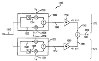
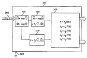
도 5는 직교 4-분기 VPA 실시예를 나타낸 예시적인 블록도이다. 원하는 전력 레벨과 주파수 특성의 출력 신호 r(t)(578)는 직교 4-분기 VPA 실시예에 따라 기저대역 동위상 및 직각위상 성분으로부터 생성된다.5 is an exemplary block diagram illustrating an orthogonal 4-branch VPA embodiment. The output signal r (t) 578 of the desired power level and frequency characteristic is generated from the baseband in-phase and quadrature components in accordance with the orthogonal 4-branch VPA embodiment.
도 5의 예에서 합성기(510)와 같은 주파수 발생기는 출력 신호 r(t)(578)의 주파수와 동일한 주파수를 가진 기준 신호 A*cos(ωt)(511)를 발생한다. 당업자라면 기준 신호는 원하는 출력 신호에 따라 선택됨을 잘 알 수 있을 것이다. 예컨대 원하는 출력 신호의 원하는 주파수가 2.4 GHz라면, 기준 신호의 주파수는 2.4 GHz로 설정된다. 이런 식으로 본 발명의 실시예는 주파수 상향 변환을 달성한다.In the example of FIG. 5, a frequency generator such as
도 5를 참조로 설명하면, 하나 또는 그 이상의 위상 분할기를 이용하여 기준 신호(511)에 기초하여 신호들(521, 531, 541, 551)을 생성한다. 도 5의 예에서 이것은 위상 분할기(512, 514, 516)를 이용하고 각 위상 분할기에서 0° 위상 천이를 적용함으로써 달성된다. 그러나 당업자라면 기준 신호(511)의 신호들(521, 531, 541, 551)을 생성하는데는 여러 가지 기법이 이용될 수 있음을 잘 알 것이다. 예컨대 1:4 위상 분할기를 이용하여 하나의 단계에서 4개의 복제 신호(521, 531, 541, 551)을 생성할 수 있으며, 또는 도 5의 예시적인 실시예에서는 신호(511)가 신호들(521, 531, 541, 551)에 바로 결합될 수 있다. 실시예에 따라서는 여러 가지 위상 천이를 적용하여 원하는 신호들(521, 531, 541, 551)을 생성할 수 있다.Referring to FIG. 5, signals 521, 531, 541, and 551 are generated based on a reference signal 511 using one or more phase dividers. In the example of FIG. 5, this is achieved by using
계속해서 도 5를 참조로 설명하면, 신호(521, 531, 541, 551)는 각각 해당 벡터 변조기(520, 530, 540, 550)에 제공된다. 벡터 변조기(520, 530, 540, 550)는 그들의 적당한 입력 신호와 관련하여 상기 수학식 (6)에 따라서 신호 r(t)의 4개의 일정 포락선 성분을 생성한다. 도 5의 예시적인 실시예에서 벡터 변조기(520, 530)는 각각 신호 r(t)의 IU(t)와 IL(t) 성분을 생성한다. 마찬가지로 벡터 변조기(540, 550)는 각각 신호 r(t)의 QU(t)와 QL(t) 성분을 생성한다.5, signals 521, 531, 541, and 551 are provided to
벡터 변조기(520, 530, 540, 550) 각각의 실제 구현은 다를 수 있다. 예컨대 당업자라면 수학식 (6)에 따라 일정 포락선 성분을 생성하는데는 여러 가지 기법이 존재함을 잘 알 것이다.The actual implementations of each of the
도 5의 예시적인 실시예에서 벡터 변조기(520, 530, 540, 550) 각각은 신호(521, 531, 541, 551)를 위상 조정(phasing)하는 입력 위상 분할기(522, 532, 542, 552)를 포함한다. 따라서 입력 위상 분할기(522, 532, 542, 552)를 이용하여 동위상 및 직각위상 성분 또는 그들 각자의 입력 신호를 생성한다.Each of the
각 벡터 변조기(520, 530, 540, 550)에서는 동위상 및 직각위상 성분은 진폭 정보와 곱해진다. 도 5에서 예컨대 승산기(524)는 신호(521)의 직각위상 성분에 IU(t)의 직각위상 진폭 정보(IUY)를 곱한다. 그와 동시에 승산기(526)는 동위상 복제 신호에 IU(t)의 동위상 진폭 정보(sgn(I)×IUX)를 곱한다.In each
IU(t)를 생성하기 위하여 일정 포락선 성분 신호(525, 527)는 위상 분할기(528) 또는 다른 합산 기술을 이용하여 합산된다. 합산 결과 신호(529)는 신호 r(t)의 IU(t) 성분에 해당한다.The constant envelope component signals 525 and 527 are summed using the phase divider 528 or other summation techniques to generate I U (t). The summing result signal 529 corresponds to the IU (t) component of the signal r (t).
전술한 것과 유사한 방식으로, 벡터 변조기(530, 540, 550)는 각각 신호 r(t)의 IL(t), QU(t) 및 QL(t) 성분을 생성한다. IL(t), QU(t) 및 QL(t)는 각각 도 5에서 신호(539, 549, 559)에 해당한다.In a manner analogous to that described above,
더욱이, 전술한 바와 같이, 신호(529, 539, 549, 559)는 실질적으로 동일하고 일정한 크기 포락선을 갖는 것을 특징으로 한다. 따라서 신호(529, 539, 549, 559)가 해당 전력 증폭기(PA)(562, 564, 566, 568)에 입력되면, 해당 증폭 신호(563, 565, 567, 569)는 실질적으로 일정한 포락선 신호이다.Moreover, as described above, the signals 529, 539, 549 and 559 are characterized by having substantially the same and constant magnitude envelope. Thus, when the signals 529, 539, 549 and 559 are input to the corresponding power amplifiers (PA) 562, 564, 566 and 568, the amplified signals 563, 565, 567 and 569 are substantially constant envelope signals .
전력 증폭기(562, 564, 566, 568)는 각각 신호(529, 539, 549, 559)를 증폭한다. 일 실시예에서, 실질적으로 동일한 전력 증폭이 각 신호(529, 539, 549, 559)에 적용된다. 일 실시예에서 PA(562, 564, 566, 568)의 전력 증폭도는 출력 신호 r(t)의 원하는 전력 레벨에 따라 설정된다.The
계속하여 도 5를 참조로 설명하면, 증폭 신호(563, 565)는 합산기(572)를 이용하여 합산되어 신호 r(t)의 동위상 성분 ![]()
![]()
![]()
![]()
신호(573, 575)는 도 5에 도시된 바와 같이 합산기(576)를 이용하여 합산되며, 합산 결과 신호가 원하는 출력 신호 r(t)에 대응한다.Signals 573 and 575 are summed using a
도 5의 예에서 합산기(572, 574, 576)는 단지 설명 목적상 사용되는 것임에 유의한다. 증폭 신호(563, 565, 567, 569)를 합산하는데는 여러 가지 기법이 이용될 수 있다. 예컨대 증폭 신호(563, 565, 567, 569)는 전부가 한 단계에서 합산되어 신호(578)를 생성할 수 있다. 실제로 본 발명의 여러 가지 VPA 실시예에 따라서 증폭후에 합산이 행해지는 것으로 충분하다. 후에 더 자세히 설명하겠지만, 본 발명의 특정 VPA 실시예는 와이어를 통한 직접 결합과 같은 최소 손실 합산 기법을 이용한다. 대안으로서 특정 VPA 실시예는 종래의 전력 결합 기법을 이용한다. 다른 실시예에서는, 후에 더 자세히 설명하겠지만, 전력 증폭기(562, 564, 566, 568)는 다중입력 단일출력 전력 증폭기로서 구현될 수 있다.It should be noted that in the example of FIG. 5 the
이제 도 6의 프로세스 플로우차트를 참조로 직교 4-분기(Cartesian 4-Branch) VPA 실시예의 동작에 대해 자세히 설명한다. 프로세스는 원하는 출력 신호의 기저대역 표기를 수신하는 것을 포함하는 단계(610)에서 개시한다. 일 실시예에서 이것은 원하는 출력 신호의 동위상(I) 성분과 직각위상(Q) 성분을 수신하는 것을 포함한다. 다른 실시예에서 이것은 원하는 출력 신호의 크기와 위상을 수신하는 것을 포함한다. 직교 4-분기 VPA 실시예의 일 실시예에서 I와 Q는 기저대역 성분이다. 다른 실시예에서 I와 Q는 RF 성분이며, 기저대역으로 하향 변환된다.The operation of the Cartesian 4-Branch VPA embodiment will now be described in detail with reference to the process flow chart of FIG. The process begins in
단계(620)는 원하는 출력 신호의 원하는 출력 신호 주파수에 따라 설정된 클록 신호를 수신하는 것을 포함한다. 도 5의 예에서 단계(620)는 기준 신호(511)를 수신함으로써 달성된다.Step 620 includes receiving a clock signal set in accordance with the desired output signal frequency of the desired output signal. In the example of FIG. 5,
단계(630)는 출력 신호 주파수를 가진 제1 및 제2 신호를 생성하기 위하여 I 성분을 처리하는 것을 포함한다. 제1 및 제2 신호는 실질적으로 일정하고 동일한 크기 포락선을 가지며 그 합은 I 성분과 같다. 제1 및 제2 신호는 전술한 IU(t) 및 IL(t) 일정 포락선 성분에 해당한다. 도 5의 예에서 단계(630)는 벡터 변조기(520, 530)에 의해 그 적당한 입력 신호와 관련하여 달성된다.Step 630 includes processing the I component to produce first and second signals having an output signal frequency. The first and second signals are substantially constant and have the same magnitude envelope, the sum being equal to the I component. The first and second signals correspond to the aforementioned I U (t) and I L (t) constant envelope components. In the example of FIG. 5,
단계(640)는 출력 신호 주파수를 가진 제3 및 제4 신호를 생성하기 위하여 Q 성분을 처리하는 것을 포함한다. 제3 및 제4 신호는 실질적으로 일정하고 동일한 크기 포락선을 가지며 그 합은 Q 성분과 같다. 제3 및 제4 신호는 전술한 QU(t) 및 QL(t) 일정 포락선 성분에 해당한다. 도 5의 예에서 단계(630)는 벡터 변조기(540, 550)에 의해 그 적당한 입력 신호와 관련하여 달성된다.Step 640 includes processing the Q component to produce third and fourth signals having an output signal frequency. The third and fourth signals have substantially constant and equal magnitude envelopes, and the sum is equal to the Q component. The third and fourth signals correspond to the Q U (t) and Q L (t) constant envelope components described above. In the example of FIG. 5,
단계(650)는 제1, 제2, 제3 및 제4 신호 각각을 개별적으로 증폭하고, 원하는 출력 신호를 생성하기 위하여 그 증폭 신호를 합산하는 것을 포함한다. 일 실시예에서 제1, 제2, 제3 및 제4 신호의 증폭은 실질적으로 동일하며, 원하는 출력 신호의 원하는 전력 레벨에 따른다. 도 5의 예에서 단계(650)는 각자의 신호(529, 539, 549, 559)를 증폭하는 전력 증폭기(562, 564, 566, 568)와 출력 신호(578)를 생성하기 위해 증폭 신호(563, 565, 567, 569)를 합산하는 합산기(572, 574, 576)에 의해 달성된다.Step 650 includes individually amplifying each of the first, second, third and fourth signals and summing the amplified signal to produce a desired output signal. In one embodiment, the amplification of the first, second, third and fourth signals is substantially the same and depends on the desired power level of the desired output signal. In the example of FIG. 5,
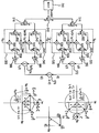
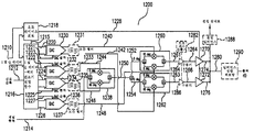
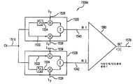
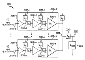
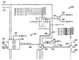
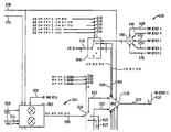
도 7a는 도 6의 프로세스 플로우차트(600)를 구현하는 벡터 전력 증폭기(700)의 예시적인 실시예를 나타낸 블록도이다. 도 7a의 예에서 선택 성분은 파선으로 나타낸다. 다른 실시예에서 추가적인 성분이 선택적일 수 있다.7A is a block diagram illustrating an exemplary embodiment of a
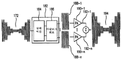
벡터 전력 증폭기(700)는 동위상(I) 분기(703)와 직각위상(Q) 분기(705)를 포함한다. I 및 Q 분기 각각은 제1 분기와 제2 분기를 더 포함한다.
동위상(I) 정보 신호(702)는 I 데이터 전달 함수 모듈(710)에 의해 수신된다. 일 실시예에서 I 정보 신호(702)는 디지털 기저대역 신호를 포함한다. 일 실시예에서 I 데이터 전달 함수 모듈(710)은 샘플 클록(706)에 따라서 I 정보 신호(702)를 샘플링한다. 다른 실시예에서 I 정보 신호(702)는 아날로그 기저대역 신호를 포함하며, 이 아날로그 기저대역 신호는 I 데이터 전달 함수 모듈(710)에 입력되기 전에 아날로그-디지털 변환기(ADC)(도 7a에는 미도시)를 이용하여 디지털로 변환된다. 다른 실시예에서 I 정보 신호(702)는 아날로그 회로를 포함하는 I 데이터 전달 함수 모듈(710)에 아날로그 형태로 입력되는 아날로그 기저대역 신호를 포함한다. 다른 실시예에서 I 정보 신호(702)는 전술한 임의의 실시예를 이용하여 I 데이터 전달 함수 모듈(710)에 입력되기 전에 기저대역으로 하향 변환되는 RF 신호를 포함한다.In-phase (I)
I 데이터 전달 함수 모듈(710)은 I 정보 신호(702)를 처리하고, I 정보 신호(702)의 적어도 2개의 일정 포락선 성분 신호의 동위상 및 직각위상 진폭 정보를 결정한다. 도 5를 참조로 전술한 바와 같이, 동위상 및 직각위상 벡터 변조기 입력 진폭 정보는 각각 sgn(I)×IUX 및 IUY에 해당한다. I 데이터 전달 함수 모듈(710)의 동작에 대해서는 뒤에 3.4 절에서 자세히 설명한다. I data transfer
I 데이터 전달 함수 모듈(710)은 벡터 변조기(760, 762)의 동위상 및 직각위상 진폭 성분을 제어하는데 이용되는 정보 신호(722, 724)를 출력한다. 일 실시예에서 신호(722, 724)는 디지털 신호이다. 따라서 각 신호(722, 724)는 각각 해당 디지털-아날로그 변환기(DAC)(730, 732)에 공급된다. DAC(730, 732)의 분해능과 샘플 레이트는 출력 신호(782)의 원하는 I 성분을 얻도록 선택된다. DAC(730, 732)는 각각 DAC 클록 신호(723, 725)에 의해 제어된다. DAC 클록 신호(723, 725)는 같은 클록 신호로부터 도출되거나 서로 독립적일 수 있다.I data transfer
다른 실시예에서 신호(722, 724)는 아날로그 신호이며, DAC(730, 732)는 필요하지 않다.In another embodiment, signals 722 and 724 are analog signals, and
도 7a의 예시적인 실시예에서 DAC(730, 732)는 디지털 정보 신호(722, 724)는 대응하는 아날로그 신호로 변환하며, 이들 아날로그 신호를 각각 선택적인 보간 필터(731, 733)에 입력한다. 안티앨리어싱(anti-aliasing) 필터로도 기능하는 보간 필터(731, 733)는 원하는 출력 파형을 만들기 위하여 DAC 출력을 정형(shaping)한다. 보간 필터(731, 733)는 각각 신호(740, 742)를 생성한다. 신호(741)는 신호(740)의 반전을 나타낸다. 신호(740-742)는 벡터 변조기(760, 762)에 입력된다.7A, the
벡터 변조기(760, 762)는 I 정보 신호(702)의 일정 포락선 성분을 생성하기 위하여 신호(740-742)를 적당히 위상 조정된 클록 신호에 곱한다. 이 클록 신호는 원하는 출력 신호 주파수에 따른 레이트를 가진 채널 클록 신호(708)로부터 도출된다. 예컨대 750과 752와 같은 복수의 위상 분할기와, 벡터 변조기 승산기와 연관된 페이저를 이용하여 적당히 위상 조정된 클록 신호를 생성할 수 있다.The
도 7a의 실시예에서, 예컨대 벡터 변조기(760)는 직각위상 진폭 정보 신호(740)를 가지고 90° 천이된 채널 클록 신호를 변조한다. 이와 동시에 벡터 변조기(760)는 동위상 진폭 정보 신호(742)를 가지고 동위상 채널 클록 신호를 변조한다. 벡터 변조기(760)는 이 2개의 변조 신호를 결합하여 I 정보 신호(702)의 제1 변조 일정 포락선 성분(761)을 생성한다. 마찬가지로 벡터 변조기(762)는 신호(741, 742)를 이용하여 I 정보 신호(702)의 제2 변조 일정 포락선 성분(763)을 생성한다. 신호(761, 763)는 각각 도 5를 참조로 설명된 IU(t) 및 IL(t) 일정 포락선 성분에 해당한다.7A, for example, the
이와 동시에 그리고 이와 유사한 방식으로 벡터 전력 증폭기(700)의 q 분기는 직각위상(Q) 정보 신호(704)의 적어도 2개의 일정 포락선 성분 신호를 생성한다.At the same time and in a similar manner, the q branch of the
도 7a의 실시예에서, 예컨대 벡터 변조기(764)는 신호(744, 746)를 이용하여 Q 정보 신호(704)의 제1 일정 포락선 성분(765)을 생성한다. 마찬가지로 벡터 변조기(766)는 신호(745, 746)를 이용하여 Q 정보 신호(704)의 제2 일정 포락선 성분(767)을 생성한다.7A, a
도 5를 참조로 전술한 바와 같이, 성분 신호(761, 763, 765, 767)는 실질적으로 동일하고 일정한 크기 포락선을 갖고 있다. 도 7a의 예시적인 실시예에서 신호(761, 763, 765, 767)는 각각 해당 전력 증폭기(PA)(770, 772, 774, 776)에 입력된다. PA(770, 772, 774, 776)는 선형 또는 비선형 전력 증폭기일 수 있다. 일 실시예에서 PA(770, 772, 774, 776)는 스위칭 전력 증폭기를 포함한다.As described above with reference to Fig. 5, component signals 761, 763, 765, and 767 have substantially the same and constant magnitude envelope. In the exemplary embodiment of FIG. 7A, signals 761, 763, 765, and 767 are input to corresponding power amplifiers (PA) 770, 772, 774, and 776, respectively.
이 실시예에서 회로(714, 716)(여기서는 참조가 용이하게 "오토바이어스(autobias) 회로"라 칭하지만 이에 제한되지 않음)는 I 및 Q 정보 신호(702, 704)에 따라 PA(770, 772, 774, 776)의 바이어스를 제어한다. 도 7a의 실시예에서 오토바이어스 회로(714, 716)는 각각 PA(770, 772)와 PA(774, 776)에 바이어스 신호(715, 717)를 제공한다. 오토바이어스 회로(714, 716)에 대해서는 이후 3.5 절에서 자세히 설명한다. PA(770, 772, 774, 776)의 실시예에 대해서도 이후 3.5 절에서 설명한다.In this embodiment,
일 실시예에서 PA(770, 772, 774, 776)는 실질적으로 동일한 전력 증폭을 각자의 실질적으로 일정한 포락선 신호(761, 763, 765, 767)에 인가한다. 다른 실시예에서는 PA 구동기를 추가적으로 채용하여 추가적인 전력 증폭을 제공한다. 도 7a의 실시예에서 PA 구동기(794, 795, 796, 797)는 벡터 전력 증폭기(700)의 각 분기에서 각자의 벡터 변조기(760, 762, 764, 766)와 각자의 PA(770, 772, 774, 776) 사이에 선택적으로 부가된다.In one embodiment,
PA(770, 772, 774, 776)의 출력은 함께 결합되어 벡터 전력 증폭기(700)의 출력 신호(782)를 생성한다. 일 실시예에서 PA(770, 772, 774, 776)의 출력은 와이어를 이용하여 함께 직접 결합된다. 이런 식의 직접 결합은 PA(770, 772, 774, 776)의 출력들 간에 저항성, 유도성 또는 용량성 결합이 극소이거나 없다는 것을 의미한다. 즉, PA(770, 772, 774, 776)의 출력은 성분 간섭 없이 함께 결합된다. 대안으로서, 일 실시예에서 PA(770, 772, 774, 776)의 출력은 임피던스 연결을 작게하거나 최소화하는 인덕턴스 및/또는 커패시턴스를 통해, 그리고/또는 절연과 전력 손실을 최소화하는 소정 연결부를 통해 간접적으로 함께 결합된다. 대안으로서, PA(770, 772, 774, 776)의 출력은 윌킨슨(Wilkinson), 하이브리드, 변압기 또는 공지의 능동 결합기와 같은 공지의 결합 기술을 이용하여 결합된다. 일 실시예에서 PA(770, 772, 774, 776)는 한 번의 동작으로 통합된 증폭과 전력 결합을 제공한다. 일 실시예에서 여기서 설명된 전력 증폭기 및/또는 구동기들 중 하나 또는 그 이상은 다중입력 단일출력 전력 증폭 기술을 이용하여 구현되며, 그 예는 도 7b 및 도 51a 내지 51h에 나타나 있다.The outputs of the
출력 신호(782)는 I 및 Q 정보 신호(702, 704)의 I 및 Q 특성을 포함한다. 더욱이, 출력 신호(782)는 그 성분과 주파수가 동일하며, 따라서 원하는 상향 변환 출력 주파수를 갖는다. 벡터 전력 증폭기(700)의 실시예에서 풀업 임피던스(780)는 벡터 증폭기(700)의 출력과 전원 장치 사이에 연결된다. 본 발명의 전력 증폭 방법 및 시스템에 따른 출력단 실시예에 대해서는 이후의 3.5 절에서 자세히 설명한다.The
벡터 전력 증폭기(700)의 다른 실시예에서는 프로세스 검출기를 채용하여 증폭기의 회로에서의 임의의 프로세스 변동을 보상한다. 도 7a의 실시예에서, 예컨대 프로세스 검출기(791-793)는 선택적으로 추가되어 PA 구동기(794-797)와 위상 분할기(750)에서의 변동을 모니터한다. 또 다른 실시예에서는 주파수 보상 회로(799)를 채용하여 주파수 변동을 보상할 수 있다.In another embodiment of the
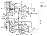
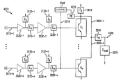
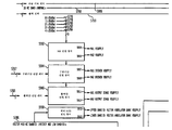
도 7b는 벡터 전력 증폭기(700)의 다른 예시적인 실시예를 나타낸 블록도이다. 선택적 성분은 파선으로 나타내며, 다른 실시예에서는 이러한 선택적 성분은 가감될 수 있다.FIG. 7B is a block diagram illustrating another exemplary embodiment of a
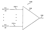
이 실시예는 도 7a의 증폭기의 다중입력 단일출력(MISO) 구현을 보여준다. 도 7b의 실시예에서 벡터 변조기(760, 762, 764, 766)로부터 출력된 일정 포락선 신호(761, 763, 765, 767)는 MISO PA(784, 786)에 입력된다. MISO PA(784, 786)는 2-입력 단일출력 전력 증폭기이다. 일 실시예에서 MISO PA(784, 786)는 도 7a의 실시예에 나타난 요소(770, 772, 774, 776, 794-797) 또는 그 기능적 등가물을 포함한다. 다른 실시예에서 MISO PA(784, 786)는 선택적인 전치 구동기와 선택적인 프로세스 검출 회로와 같은 다른 요소를 포함할 수 있다. 더욱이 MISO PA(784, 786)는 도 7b에 도시된 2-입력 PA에 한정되지 않는다. 다른 실시예에서, 이후 도 51a 내지 51h를 참조로 자세히 설명되겠지만, PA(784, 786)는 임의 수의 입력과 출력을 가질 수 있다.This embodiment shows a multiple input single output (MISO) implementation of the amplifier of FIG. 7A. The constant envelope signals 761, 763, 765, and 767 output from the
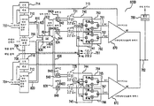
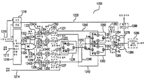
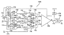
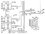
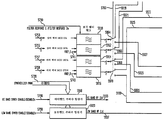
도 8a는 도 6에 도시된 직교 4-분기 VPA법에 따른 벡터 전력 증폭기의 다른 예시적인 실시예(800A)를 나타낸 블록도이다. 선택적 성분은 파선으로 나타내며, 다른 실시예에서는 이러한 선택적 성분은 가감될 수 있다.8A is a block diagram illustrating another
도 8a의 실시예에서는 충분한 분해능과 샘플 레이트를 가진 DAC(830)는 도 7a의 실시예의 DAC(730, 732, 734, 736)를 대체한다. DAC(830)의 샘플 레이트는 DAC 클록 신호(826)에 의해 제어된다.8A, the
DAC(830)는 전술한 바와 같이 I 데이터 전달 함수 모듈(710) 및 Q 데이터 전달 함수 모듈(712)로부터 각각 동위상 및 직각위상 정보 신호(810, 820)를 수신한다. 일 실시예에서 입력 선택기(822)는 DAC(830)에 입력되는 신호(810, 820)의 순서를 선택한다.
DAC(830)는 한 번에 하나의 아날로그 신호를 출력할 수 있다. 일 실시예에서는 샘플 홀드 구조를 이용하여 도 8a에 도시된 바와 같이 증폭기의 4개 분기에 대한 적당한 신호 타이밍을 보장할 수 있다.The
DAC(830)는 아날로그 신호(832, 834, 836, 838)를 제1 샘플 홀드 회로 세트(842, 844, 846, 848)에 순차적으로 출력한다. 일 실시예에서 DAC(830)는 도 7a의 실시예의 DAC(730, 732, 734, 736)의 동작을 에뮬레이트하기에 충분한 레이트로 클록된다. 출력 선택기(824)는 출력 신호(832, 834, 836, 838) 중 어느 것이 출력으로 선택되어야 하는지를 판단한다.The
DAC(830)의 DAC 클록 신호(826), 출력 선택기 신호(824), 입력 선택기 신호(822) 및 샘플 홀드 클록(840A-D, 850)은 독립적이거나 또는 전달 함수 모듈(710 및/또는 712)에 집적될 수 있는 제어 모듈에 의해 제어된다.The
일 실시예에서 샘플 홀드 회로(S/H)(842, 844, 846, 848)는 클록 신호(840A-D)에 따라서 DAC(830)로부터 수신된 아날로그값을 샘플링하여 홀드한다. 샘플 홀드 회로(852, 854, 856, 858)는 각각 샘플 홀드 회로(842, 844, 846, 848)로부터의 아날로그값을 샘플링하여 홀드한다. 이어서, 샘플 홀드 회로(852, 854, 856, 858)는 수신된 아날로그값을 홀드하고, 공통 클록 신호(850)에 따라서 그 값을 벡터(760, 762, 764, 766)에 동시에 방출한다. 다른 실시예에서 샘플 홀드 회로(852, 854, 856, 858)는 그 값을 선택적인 보간 필터(731, 733, 735, 737)(안티앨리어싱 필터라고도 함)에 방출한다. 일 실시예에서 공통 클록 신호(850)는 S/H(852, 854, 856, 858)의 출력이 시간 정렬되는 것을 보장하도록 이용된다.In one embodiment, the sample-and-
벡터 전력 증폭기(800A)의 다른 양상은 벡터 전력 증폭기(700)에 대해 전술한 것과 거의 같다.Another aspect of the
도 8b는 도 6에 도시된 직교 4-분기 VPA법에 따른 벡터 전력 증폭기의 다른 예시적인 실시예(800B)를 나타낸 블록도이다. 선택적 성분은 파선으로 나타내며, 다른 실시예에서는 이러한 선택적 성분은 가감될 수 있다.8B is a block diagram illustrating another
실시예(800B)는 벡터 전력 증폭기의 다른 하나의 DAC 구현을 보여준다. 그러나 도 8a의 실시예와는 달리, 샘플 홀드 구조는 단일 세트의 샘플 홀드(S/H) 회로를 포함한다. 도 8b에 도시된 바와 같이 S/H(842, 844, 846, 848)는 DAC(830)로부터 신호(832, 834, 836, 838)로 나타낸 아날로그값을 수신한다. S/H 회로(842, 844, 846, 848) 각각은 그 수신값을 도시된 바와 같은 여러 가지 클록(840A-D)에 따라서 방출한다. 신호(740, 741, 742, 744, 745, 746)를 생성하는데 이용되는 아날로그 샘플들 간의 시간차는 전달 함수(710, 712)에서 보상될 수 있다. 도 8b의 실시예에 따르면 도 8a의 실시예에 비해 한 레벨의 S/H 회로가 생략될 수 있어 증폭기의 크기와 복잡성을 저감할 수 있다.Example (800B) shows another DAC implementation of a vector power amplifier. However, unlike the embodiment of FIG. 8A, the sample and hold structure includes a single set of sample hold (S / H) circuits. 842, 844, 846, 848 receive analog values represented by
벡터 전력 증폭기(800B)의 다른 양상은 벡터 전력 증폭기(700, 800A)에 대해 전술한 것과 거의 같다.Another aspect of the
도 8c는 벡터 전력 증폭기(700)의 다른 예시적인 실시예(800C)를 나타낸 블록도이다. 선택적 성분은 파선으로 나타내며, 다른 실시예에서는 이러한 선택적 성분은 가감될 수 있다. 도 8c의 실시예는 도 8a의 증폭기의 다중입력 단일출력(MISO) 구현을 보여준다. 도 8c의 실시예에서 벡터 변조기(760, 762, 764, 766)로부터 출력된 일정 포락선 신호(761, 763, 765, 767)는 MISO PA(860, 862)에 입력된다. MISO PA(860, 862)는 2-입력 단일출력 전력 증폭기이다. 일 실시예에서 MISO PA(860, 862)는 도 7a의 실시예에 나타난 요소(770, 772, 774, 776, 794-797) 또는 그 기능적 등가물을 포함한다. 다른 실시예에서 MISO PA(860, 862)는 선택적인 전치 구동기와 선택적인 프로세스 검출 회로와 같은 다른 요소를 포함할 수 있다. 다른 실시예에서 MISO PA(860, 862)는 도 7a의 실시예에는 없는 전치 구동기와 같은 다른 요소를 포함할 수 있다. 더욱이 MISO PA(860, 862)는 도 8c에 도시된 2-입력 PA에 한정되지 않는다. 다른 실시예에서, 이후 도 51a 내지 51h를 참조로 자세히 설명되겠지만, PA(860, 862)는 임의 수의 입력과 출력을 가질 수 있다.FIG. 8C is a block diagram illustrating another exemplary embodiment 800C of the
벡터 전력 증폭기(800C)의 다른 양상은 벡터 전력 증폭기(700, 800A)에 대해 전술한 것과 거의 같다.Another aspect of the vector power amplifier 800C is substantially the same as described above for the
도 8d는 벡터 전력 증폭기(700)의 다른 예시적인 실시예(800D)를 나타낸 블록도이다. 선택적 성분은 파선으로 나타내며, 다른 실시예에서는 이러한 선택적 성분은 가감될 수 있다. 도 8d의 실시예는 도 8b의 증폭기의 다중입력 단일출력(MISO) 구현을 보여준다. 도 8d의 실시예에서 벡터 변조기(760, 762, 764, 766)로부터 출력된 일정 포락선 신호(761, 763, 765, 767)는 MISO PA(870, 872)에 입력된다. MISO PA(870, 872)는 2-입력 단일출력 전력 증폭기이다. 일 실시예에서 MISO PA(870, 872)는 도 7a의 실시예에 나타난 요소(770, 772, 774, 776, 794-797) 또는 그 기능적 등가물을 포함한다. 다른 실시예에서 MISO PA(870, 872)는 선택적인 전치 구동기와 선택적인 프로세스 검출 회로와 같은 다른 요소를 포함할 수 있다. 다른 실시예에서 MISO PA(870, 872)는 도 7a의 실시예에는 없는 전치 구동기와 같은 다른 요소를 포함할 수 있다. 더욱이 MISO PA(870, 872)는 도 8d에 도시된 2-입력 PA에 한정되지 않는다. 다른 실시예에서, 이후 도 51a 내지 51h를 참조로 자세히 설명되겠지만, PA(870, 872)는 임의 수의 입력과 출력을 가질 수 있다.FIG. 8D is a block diagram illustrating another
벡터 전력 증폭기(800D)의 다른 양상은 벡터 전력 증폭기(700, 800B)에 대해 전술한 것과 거의 같다.
Another aspect of the
3.2) 직교-극-직교-극 2-분기 벡터 전력 증폭기3.2) Orthogonal-pole-to-orthogonal-pole 2-branch vector power amplifier
이제 직교-극-직교-극(CPCP) 2-분기 VPA 실시예에 대해 설명한다(이러한 실시예 명칭은 참조를 용이하게 하기 위해 제시된 것이며 이에 한정되는 것은 아니다).Now, an orthogonal-pole-quadrature-pole (CPCP) two-branch VPA embodiment will be described (these embodiment names are presented for ease of reference and not limitation).
직교-극-직교-극(CPCP) 2-분기 VPA법에 따라서 시변 복소 포락선 신호는 2개의 실질적으로 일정한 포락선 성분 신호로 분해된다. 이 성분 신호들은 개별적으로 증폭된 다음에 합산되어 원래의 시변 복소 포락선 신호의 증폭 신호를 구성한다. 게다가 시변 복소 포락선 신호의 위상각은 확정되어 있으며, 성분 신호의 합산 결과는 적당한 각도만큼 위상 천이된다.Orthogonal-polar-orthogonal-polar (CPCP) In accordance with the two-branch VPA method, the time-varying complex envelope signal is decomposed into two substantially constant envelope component signals. These component signals are separately amplified and then summed to construct an amplified signal of the original time varying complex envelope signal. In addition, the phase angle of the time-varying complex envelope signal is fixed, and the sum of the component signals is phase-shifted by an appropriate angle.
CPCP 2-분기 VPA법의 일 실시예에서 시변 복소 포락선 신호의 크기와 위상각은 신호의 동위상 및 직각위상 성분으로부터 산출된다. 크기 정보가 주어지면 2개의 실질적으로 일정한 포락선 성분은 원하는 시변 포락선 신호의 정규화 버전으로부터 산출되는데, 이 정규화는 위상 및/또는 진폭의 구현 특정 조작을 포함한다. 그러면, 이 2개의 실질적으로 일정한 포락선 성분은 원하는 시변 포락선 신호의 위상 천이에 관련된 적당한 각도만큼 위상 천이된다. 그 다음 이 실질적으로 일정한 포락선 성분들은 개별적으로 거의 똑 같이 증폭된 다음에 합산되어 원래의 원하는 시변 포락선 신호의 증폭 버전을 생성한다.In one embodiment of the CPCP two-branch VPA method, the magnitude and phase angle of the time-varying complex envelope signal is computed from the in-phase and quadrature components of the signal. Given the size information, two substantially constant envelope components are computed from the normalized version of the desired time-varying envelope signal, which includes implementation specific operations of phase and / or amplitude. Then, these two substantially constant envelope components are phase shifted by an appropriate angle related to the phase shift of the desired time-varying envelope signal. The substantially constant envelope components are then separately amplified nearly equally and then summed to produce an amplified version of the original desired time-varying envelope signal.
도 9a 및 9b는 페이저 신호 표기를 이용한 CPCP 2-분기 VPA 실시예를 개념적으로 보여준다. 도 9a에서 페이저 ![]()
![]()
![]()
![]()
![]()
![]()
도 9a를 참조로 설명하면, ![]()
![]()
![]()
![]()
![]()
![]()
![]()
![]()
계속해서 도 9a를 참조로 설명하면, 임의 순간에서 ![]()
![]()
![]()
![]()
![]()
![]()
![]()
![]()
![]()
![]()
![]()
![]()
![]()
![]()
![]()
![]()
![]()
![]()
![]()
![]()
![]()
![]()
![]()
![]()
![]()
![]()
![]()
![]()
![]()
![]()
![]()
![]()
![]()
![]()
![]()
![]()
도 9a에 나타낸 경우에 있어서 ![]()
![]()
![]()
![]()
![]()
![]()
![]()
![]()
![]()
![]()

여기서 R은 페이저 ![]()
![]()
수학식 (7)은 다은과 같이 더 간단하게 될 수 있다.Equation (7) can be simplified as follows.

여기서 R은 페이저 ![]()
![]()
대안으로서, 임의의 실질적으로 등가적인 수학식이나 탐색표와 같은 다른 실질적으로 등가적인 수학적 기법이 이용될 수 있다.Alternatively, other substantially equivalent mathematical techniques such as any substantially equivalent mathematical equations or search tables may be used.
상기 설명으로부터 페이저 표기에서 가변 크기와 위상의 임의 페이저 ![]()
![]()

이에 대응하여, 시간 영역에서 시변 복소 포락선 정현파 신호 r'(t)=R(t)×cos(ωt)는 다음과 같이 2개의 일정 포락선 신호의 합으로 구성된다.Corresponding to this, in the time domain, the time-varying complex envelope sinusoidal signal r '(t) = R (t) × cos (ωt) consists of the sum of two constant envelope signals as follows.

여기서 A는 상수이며, ![]()
![]()
도 9a로부터 수학식(9)는 다음과 같이 다시 쓸 수 있음을 검증할 수 있다.From FIG. 9A, it can be verified that equation (9) can be rewritten as follows.

여기서 C는 페이저 페이저 ![]()
![]()
![]()
![]()
![]()
![]()
![]()
![]()
![]()
![]()
![]()
![]()
![]()
![]()
![]()
![]()
![]()
![]()
![]()
![]()
![]()
![]()

수학식 (11)은 ![]()
![]()
![]()
![]()
![]()
![]()
![]()
![]()
![]()
![]()
![]()
![]()
![]()
![]()
![]()
![]()
![]()
![]()
![]()
![]()
![]()
![]()
![]()
![]()
![]()
![]()
![]()
![]()
![]()
![]()
![]()
![]()
![]()
![]()
![]()
![]()
![]()
![]()
등가적으로 시간 영역에서 다음과 같이 될 수 있다.Equivalently, in the time domain,

![]()
![]()
![]()
![]()
![]()
![]()
당업자라면 수학식 (9)와 (10)의 시간 영역 표현은 정현파형의 경우에 대해 제공되었지만 적당한 기본 함수를 이용하여 비정현파형에 대해서도 동등한 표현이 전개될 수 있음을 잘 알 것이다. Those skilled in the art will appreciate that the time domain representations of equations (9) and (10) are provided for sinusoidal cases, but equivalent expressions can also be developed for non sinusoidal types using appropriate basic functions.
도 10은 CPCP 2-분기 VPA 실시예의 예시적인 실시예(1000)를 개념적으로 나타낸 블록도이다. 원하는 전력 레벨와 주파수 특성을 갖는 출력 신호 r(t)는 CPCP 2-분기 VPA 실시예에 따라 동위상 및 직각위상 성분으로부터 생성된다.10 is a block diagram conceptually illustrating an
도 10의 예에서 클록 신호(1010)는 출력 신호 r(t)를 생성하기 위한 기준 신호를 나타낸다. 클록 신호(1010)는 원하는 출력 신호 r(t)와 주파수가 동일하다.In the example of FIG. 10, the
도 10을 참조로 설명하면, Iclk_위상 신호(1012)와 Qclk_위상 신호(1014)는 Clk 신호(1010)의 동위상 및 직각위상 성분이 곱해진 진폭 아날로그값을 나타내며 기저대역 I 및 Q 신호로부터 산출된다.10, the
계속해서 도 10을 참조로 설명하면, 클록 신호(1010)에 Iclk_위상 신호(1012)가 곱해진다. 이와 동시에 클록 신호(1010)의 90° 천이된 버전에 Qclk_위상 신호(1014)가 곱해진다. 이 2개의 곱해진 신호는 결합되어 Rclk 신호(1016)를 생성한다. Rclk 신호(1016)는 클록 신호(1010)와 주파수가 같다. 더욱이 Rclk 신호(1016)는 Q(t)와 I(t)의 비에 따른 위상 천이각에 의해 특징지워진다. Rclk 신호(1016)의 크기는 R2clk=I2clk_위상+Q2clk_위상과 같다. 따라서 Rclk 신호(1016)는 원하는 출력 신호 r(t)의 위상 특성을 가진 실질적으로 일정한 포락선 신호를 나타낸다.Continuing with reference to FIG. 10, the
계속해서 도 10을 참조로 설명하면, Rclk 신호(1016)는 2개의 벡터 변조기(1060, 1062)에 동시에 입력된다. 벡터 변조기(1060, 1062)는 각각 수학식 (12)에 기술된 원하는 출력 신호 r(t)의 실질적으로 일정한 U(t) 및 L(t) 포락선 성분을 생성한다. 벡터 변조기(1060)에서는 공통 신호(1028)가 곱해진 동위상 Rclk 신호(1020)가, 제1 신호(1026)가 곱해진 Rclk 신호의 90° 천이된 버전(1018)과 결합된다. 이와 동시에, 벡터 변조기(1062)에서는 공통 신호(1028)가 곱해진 동위상 Rclk 신호(1022)가, 제2 신호(1030)가 곱해진 Rclk 신호의 90° 천이된 버전(1024)과 결합된다. 공통 신호(1028), 제1 신호(1026) 및 제2 신호(1030)는 각각 수학식 (12)에 기술된 실수부 C, 허수부 α 및 β에 해당한다.Continuing with reference to FIG. 10, the
각자의 벡터 변조기(1060, 1062)의 출력 신호(1040, 1042)는 각각 입력 신호 r(t)의 U(t) 및 L(t) 일정 포락선 성분에 해당한다.The output signals 1040 and 1042 of the
전술한 바와 같이 신호(1040, 1042)는 실질적으로 동일하고 일정한 크기 포락선을 갖는 것을 특징으로 한다. 따라서 신호(1040, 1042)가 해당 전력 증폭기(PA)(1044, 1046)에 입력되면, 해당 증폭 신호(1048, 1050)는 실질적으로 일정한 포락선 신호이다.As described above, the
전력 증폭기(1044, 1046)는 실질적으로 동일한 전력 증폭을 각각 신호(1040, 1042)에 적용한다. 일 실시예에서 PA(1044, 1046)의 전력 증 레벨을 출력 신호 r(t)의 원하는 전력 레벨에 따라 설정된다. 더욱이 증폭 신호(1048, 1050)는 서로에 대해 동위상이다. 따라서 도 10에 도시된 바와 같이 증폭 신호들이 합산되면, 그 합산 결과 신호(1052)는 원하는 출력 신호 r(t)에 해당한다.
도 10a는 CPCP 2-분기 VPA 실시예의 다른 예시적인 실시예(1000A)를 보여준다. 실시예(1000A)는 도 10의 실시예(1000)의 다중입력 단일출력(MISO) 구현을 나타낸다.10A shows another
실시예(1000A)에서 벡터 변조기(1060, 1062)로부터 출력된 일정 포락선 신호(1040, 1042)는 MISO PA(1054)에 입력된다. MISO PA(1054)는 2-입력 단일출력 전력 증폭기이다. 일 실시예에서 MISO PA(1054)는 예컨대 전치 구동기, 구동기, 전력 증폭기 및 프로세스 검출기(도 10a에는 미도시)와 같은 여러 가지 요소를 포함할 수 있다. 더욱이 MISO PA(1054)는 도 10a에 도시된 2-입력 PA에 한정되지 않는다. 다른 실시예에서, 이후 도 51a 내지 51h를 참조로 자세히 설명되겠지만, PA(1054)는 임의 수의 입력을 가질 수 있다.The
CPCP 2-분기 VPA 실시예의 동작은 도 11의 프로세스 플로우차트(1100)에 나타나 있다.The operation of the CPCP 2-branch VPA embodiment is shown in the
프로세스는 원하는 출력 신호의 기저대역 표기를 수신하는 것을 포함하는 단계(1110)에서 개시한다. 일 실시예에서 이것은 원하는 출력 신호의 동위상(I) 성분과 직각위상(Q) 성분을 수신하는 것을 포함한다. 다른 실시예에서 이것은 원하는 출력 신호의 크기와 위상을 수신하는 것을 포함한다.The process begins in
단계(1120)는 원하는 출력 신호의 원하는 출력 신호 주파수에 따라 설정된 클록 신호를 수신하는 것을 포함한다. 도 10의 예에서 단계(1120)는 클록 신호(1010)를 수신함에 의해 달성된다.
단계(1130)는 수신된 I 및 Q 성분에 따라서 위상 천이각을 가진 정규화된 클록 신호를 생성하기 위하여 클록 신호를 처리하는 것을 포함한다. 일 실시예에서 정규화된 클록 신호는 I와 Q 성분의 비에 따라서 위상 천이각을 가진 일정 포락선 신호이다. 정규화된 클록의 위상 천이각은 원래의 클록 신호에 대한 것이다. 도 10의 예에서 단계(1130)는 클록 신호(1010)의 동위상 및 직각위상 성분을 Iclk_위상(1012) 및 Qclk_위상(1014) 신호에 곱한 다음에, 곱해진 신호를 합산하여 Rclk 신호(1016)를 생성함으로써 달성된다.
단계(1140)는 제1 및 제2의 실질적으로 일정한 포락선 성분 신호를 생성하는데 필요한 진폭 정보를 발생하기 위하여 I 및 Q 성분을 처리하는 것을 포함한다.
단계(1150)는 원하는 출력 신호의 제1 및 제2 일정 포락선 성분을 생성하기 위하여 단계(1140)의 진폭 정보와 정규화된 클록 신호 Rclk를 처리하는 것을 포함한다. 일 실시예에서 단계(1150)는 원하는 출력 신호의 제1 및 제2 일정 포락선 성분을 정규화된 클록 신호의 위상 천이각만큼 위상 천이하는 것을 포함한다. 도 10의 예에서 단계(1150)는 신호(1040, 1042)를 생성하기 위하여 제1 신호(1026), 제2 신호(1030) 및 공통 신호(1028)를 가지고 Rclk 신호(1016)를 변조하는 벡터 변조기(1060, 1062)에 의해 달성된다.
단계(1160)는 제1 및 제2 일정 포락선 성분을 개별적으로 증폭하고, 원하는 출력 신호를 생성하기 위하여 이 증폭된 신호를 합산하는 것을 포함한다. 일 실시예에서 제1 및 제2 일정 포락선 성분의 증폭은 거의 같으며, 원하는 출력 신호의 원하는 전력 레벨에 따른다. 도 10의 예에서 단계(1160)는 증폭된 신호(1048, 1050)를 생성하기 위하여 신호(1040, 1042)를 증폭하는 PA(1044, 1046)에 의해 달성된다.
도 12는 프로세스 플로우차트(1100)를 구현하는 벡터 전력 증폭기(1200)의 예시적인 실시예를 나타낸 블록도이다. 선택적 성분은 파선으로 나타내며, 다른 실시예에서는 이러한 선택적 성분은 가감될 수 있다.Figure 12 is a block diagram illustrating an exemplary embodiment of a
도 12를 참조로 설명하면, 동위상(I) 및 직각위상(Q) 정보 신호(1210)는 I 및 Q 데이터 전달 함수 모듈(1216)에 의해 수신된다. 일 실시예에서 I 및 Q 데이터 전달 함수 모듈(1216)은 샘플 클록(1212)에 따라 신호(1210)를 샘플링한다. I 및 Q 정보 신호(1210)는 원하는 출력 신호 r(t)의 기저대역 I 및 Q 정보를 포함한다.Referring to FIG. 12, in-phase (I) and quadrature (Q) information signals 1210 are received by the I and Q data
일 실시예에서 I 및 Q 데이터 전달 함수 모듈(1216)은 정보 신호(1210)를 처리하여 정보 신호(1220, 1222, 1224, 1226)를 생성한다. I 및 Q 데이터 전달 함수 모듈(1216)의 동작에 대해서는 이후의 3.4 절에서 자세히 설명한다.In one embodiment, I and Q data
도 12를 참조로 설명하면, 정보 신호(1220)는 원하는 출력 신호 r(t)의 기저대역 버전의 제1 및 제2 일정 포락선 성분의 직각위상 진폭 정보를 포함한다. 도 9a를 참조하면, 예컨대 정보 신호(1220)는 α 및 β 직각위상 성분을 포함한다. 다시 도 12를 참조하여 설명하면, 정보 신호(1226)는 신호 r(t)의 기저대역 버전의 제1 및 제2 일정 포락선 성분의 동위상 진폭 정보를 포함한다. 도 9a를 참조하면, 예컨대 정보 신호(1226)는 공통 C 동위상 성분을 포함한다.Referring to Figure 12, the
계속해서 도 12를 참조로 설명하면, 정보 신호(1222, 1224)는 각각 정규화된 동위상 Iclk_위상 및 직각위상 Qclk_위상 신호를 포함한다. Iclk_위상 및 Qclk_위상은 신호(1210)에 포함된 I 및 Q 정보 신호의 정규화된 버전이다. 일 실시예에서 Iclk_위상 및 Qclk_위상은 (I2clk_위상+Q2clk_위상=일정)이 되도록 정규화된다. 신호(1250)의 위상은 원하는 출력 신호의 위상에 해당하며 Iclk_위상 및 Qclk_위상으로부터 생성됨에 유의한다. 도 9b를 참조로 설명하면, Iclk_위상 및 Qclk_위상은 다음과 같이 I 및 Q에 관련된다.12, information signals 1222 and 1224 include normalized in-phase Iclk_phase and quadrature-phase Qclk_phase signals, respectively. The Iclk_phase and Qclk_phase are normalized versions of the I and Q information signals contained in the

여기서 θ는 도 9b에서 페이저 ![]()
![]()
도 12의 예시적인 실시예에서 정보 신호(1220, 1222, 1224, 1226)는 디지털 신호이다. 따라서 각 신호(1220, 1222, 1224, 1226)는 해당 디지털-아날로그 변환기(DAC)(1230, 1232, 1234, 1236)에 공급된다. DAC(1230, 1232, 1234, 1236)의 분해능과 샘플 레이트는 특정 시그널링 방식에 따라 선택된다. DAC(1230, 1232, 1234, 1236)는 각각 DAC 클록 신호(1221, 1223, 1225, 1227)에 의해 제어된다. DAC 클록 신호(1221, 1223, 1225, 1227)는 동일한 클록 신호로부터 도출되거나 독립적일 수 있다.In the exemplary embodiment of FIG. 12, the information signals 1220, 1222, 1224, and 1226 are digital signals. Thus, each of the
다른 실시예에서 정보 신호(1220, 1222, 1224, 1226)는 아날로그 형식으로 생성되며, DAC는 필요치 않다.In another embodiment, the information signals 1220, 1222, 1224, and 1226 are generated in analog form, and a DAC is not required.
도 12를 참조로 설명하면, DAC(1230, 1232, 1234, 1236)는 디지털 정보 신호(1220, 1222, 1224, 1226)를 대응하는 아날로그 신호로 변환하고, 이들 아날로그 신호를 각각 선택적인 보간 필터(1231, 1233, 1235, 1237)에 입력한다. 안티앨리어싱 필터로도 기능하는 보간 필터(1231, 1233, 1235, 1237)는 DAC 출력 신호를 정형하여 원하는 출력 파형을 생성한다. 보간 필터(1231, 1233, 1235, 1237)는 각각 신호(1240, 1244, 1246, 1248)를 생성한다. 신호(1242)는 신호(1240)의 반전을 나타낸다.12,
계속해서 도 12를 참조로 설명하면, Iclk_위상 및 Qclk_위상 정보를 포함하는 신호(1244, 1246)는 벡터 변조기(1238)에 입력된다. 벡터 변조기(1238)는 신호(1244)를 채널 클록 신호(1214)에 곱한다. 채널 클록 신호(1214)는 원하는 출력 신호 주파수에 따라 선택된다. 이와 동시에 벡터 변조기(1238)는 신호(1246)를 채널 클록 신호(1214)의 90°천이된 버전에 곱한다. 즉 벡터 변조기(1238)는 Iclk_위상의 진폭을 가진 동위상 성분과 Qclk_위상의 진폭을 가진 직각위상 성분을 생성한다.12,
벡터 변조기(1238)는 이 2개의 변조 신호를 결합하여 Rclk 신호(1250)를 생성한다. Rclk 신호(1250)는 신호(1210)에 포함된 I 및 Q 데이터에 따라 원하는 출력 주파수와 위상 천이각을 가진 실질적으로 일정한 포락선 신호이다.The
계속해서 도 12를 참조로 설명하면, 신호(1240, 1242, 1248)는 각각 신호 r(t)의 복소 포락선의 U, L 및 공통 C 진폭 성분을 포함한다. 신호(1240, 1242, 1248)는 Rclk 신호(1250)와 함께 벡터 변조기(1260, 1262)에 입력된다.12,
벡터 변조기(1260)는 Rclk 신호(1250)의 90° 천이된 버전이 곱해진 신호(1240)와 Rclk 신호(1250)의 0° 천이된 버전이 곱해진 신호(1248)를 결합하여 출력 신호(1264)를 생성한다. 이와 동시에 벡터 변조기(1262)는 Rclk 신호(1250)의 90° 천이된 버전이 곱해진 신호(1242)와 Rclk 신호(1250)의 0° 천이된 버전이 곱해진 신호(1248)를 결합하여 출력 신호(1266)를 생성한다.The
출력 신호(1264, 1266)는 실질적으로 일정한 포락선 신호를 나타낸다. 더욱이 Rclk 신호(1250)에 대한 출력 신호(1264, 1266)의 위상 천이는 각각 비 α/C 및 β/C와 연관된 각도 관계에 따라 결정된다. 일 실시예에서 α=β이며, 따라서 출력 신호(1264, 1266)는 Rclk 신호(1250)에 대해 대칭적으로 위상 천이된다. 도 9b를 참조하면, 예컨대 출력 신호(1264, 1266)는 각각 ![]()
![]()
![]()
![]()
출력 신호(1264, 1266)는 합산되어 기저대역 신호 r(t)의 I 및 Q 특성을 가진 채널 클록 변조 신호가 된다. 그러나 벡터 전력 증폭기(1200)의 출력에서 원하는 전력 레벨을 얻기 위해서 신호(1264, 1266)는 증폭되어 증폭 출력 신호를 생성한다. 도 12의 실시예에서 신호(1264, 1266)는 각각 전력 증폭기(PA)(1270, 1272)에 입력되어 증폭된다. 일 실시예에서 PA(1270, 1272)는 스위칭 전력 증폭기를 포함한다. 오토바이어스 회로(1218)는 후에 3.5.2 절에서 자세히 설명하는 바와 같이 PA(1270, 1272)의 바이어스를 제어한다. 도 12의 실시예에서, 예컨대 오토바이어스 회로(1218)는 바이어스 전압(1228)을 PA(1270, 1272)에 공급한다.The output signals 1264 and 1266 are summed to become a channel clock modulated signal with the I and Q characteristics of the baseband signal r (t). However, to obtain the desired power level at the output of
일 실시예에서 PA(1270, 1272)는 실질적으로 동일한 전력 증폭을 각자의 일정 포락선 신호(1264-1266)에 적용한다. 일 실시예에서 전력 증폭은 원하는 출력 전력 레벨에 따라 설정된다. 벡터 전력 증폭기(1200)의 다른 실시예에서, PA 구동기 및/또는 전치 구동기를 추가적으로 채용하여 증폭기에 추가적인 전력 증폭 능력을 제공한다. 도 12의 실시예에서, 예컨대 PA 구동기(1284, 1286)는 각각 벡터 변조기(1260, 1262)와 그 다음의 PA(1270, 1272) 사이에 선택적으로 추가된다.In one embodiment,
PA(1270, 1272)의 각자의 출력 신호(1274, 1276)는 실질적으로 일정한 포락선 신호이다. 더욱이 출력 신호(1274, 1276)가 합산되면, 그 합산 결과 신호는 최소의 비선형 왜곡을 갖는다. 도 12의 실시예에서 출력 신호(1274, 1276)는 함께 결합되어 벡터 전력 증폭기(1200)의 출력 신호(1280)를 생성한다. 일 실시예에서 PA(1270, 1272)의 출력을 결합하는데 절연이 이용되지 않는다. 따라서 결합에 의한 전력 손실은 최소가 된다. 일 실시예에서 PA(1270, 1272)의 출력은 와이어를 이용하여 함께 직접 결합된다. 이런 식으로의 직접 결합은 PA(1270, 1272)의 출력들 간에 저항성, 유도성 또는 용량성 절연이 최소이거나 없다는 것을 의미한다. 즉 PA(1270, 1272)의 출력은 중간에 개입하는 성분없이 함께 결합된다. 대안으로서 일 실시예에서 PA(1270, 1272)의 출력은 임피던스 연결을 작게하거나 최소화하는 인덕턴스 및/또는 커패시턴스를 통해, 그리고/또는 절연과 전력 손실을 최소화하는 소정 연결부를 통해 간접적으로 함께 결합된다. 대안으로서, PA(1270, 1272)의 출력은 윌킨슨, 하이브리드 결합기, 변압기 또는 공지의 능동 결합기와 같은 공지의 결합 기술을 이용하여 결합된다. 일 실시예에서 PA(1270, 1272)는 한 번의 동작으로 통합된 증폭과 전력 결합을 제공한다. 일 실시예에서 여기서 설명된 전력 증폭기 및/또는 구동기들 중 하나 또는 그 이상은 다중입력 단일출력 전력 증폭 기술을 이용하여 구현되며, 그 예는 도 12a, 12b 및 도 51a 내지 51h에 나타나 있다.The output signals 1274 and 1276 of each of the
출력 신호(1280)는 기저대역 신호 r(t)의 I 및 Q 특성과 원하는 출력 전력 레벨 및 주파수를 가진 신호를 나타낸다. 벡터 전력 증폭기(1200)의 실시예에서 풀업(pull-up) 임피던스(1288)는 벡터 전력 증폭기(1200)의 출력과 전원 장치 사이에 연결된다. 다른 실시예에서 임피던스 정합 회로망(1290)은 벡터 전력 증폭기(1200)의 출력에 연결된다. 본 발명의 전력 증폭 방법 및 시스템에 따른 출력단 실시예에 대해서는 이후의 3.5 절에서 자세히 설명한다.The
벡터 전력 증폭기(1200)의 다른 실시예에서는 프로세스 검출기를 채용하여 증폭기의 회로에서의 프로세스 변동을 보상한다. 도 12의 예시적인 실시예에서, 예컨대 프로세스 검출기(1282)는 선택적으로 추가되어 PA 구동기(1284, 1286)에서의 변동을 모니터한다.In another embodiment of the
도 12a는 프로세스 플로우차트(1100)를 구현하는 벡터 전력 증폭기(1200A)의 다른 예시적인 실시예를 나타낸 블록도이다. 선택적 성분은 파선으로 나타내며, 다른 실시예에서는 이러한 선택적 성분은 가감될 수 있다.12A is a block diagram illustrating another exemplary embodiment of a
실시예(1200A)는 실시예(1200)의 다중입력 단일출력(MISO) 구현을 나타낸다. 실시예(1200A)에서 벡터 변조기(1260, 1262)로부터 출력된 일정 포락선 신호(1261, 1263)는 MISO PA(1292)에 입력된다. MISO PA(1292)는 2-입력 단일출력 전력 증폭기이다. 일 실시예에서 MISO PA(1292)는 도 12의 실시예에 나타낸 요소(1270, 1272, 1282, 1284, 1286)를 포함한다. 다른 실시예에서 MISO PA(1292)는 도 12의 실시예에는 나타나 있지 않은 전치 구동기와 같은 다른 요소를 포함할 수 있다. 더욱이 MISO PA(1292)는 도 12a에 도시된 2-입력 PA에 한정되지 않는다. 다른 실시예에서, 이후 도 51a 내지 51h를 참조로 자세히 설명되겠지만, PA(1292)는 임의 수의 입력과 출력을 가질 수 있다.
계속해서 도 12a를 참조로 설명하면, 실시예(1200A)는 오토바이어스 신호를 MISO PA(1292)에 전달하는 일 구현을 보여준다. 도 12a의 실시예에서 오토바이어스 회로(1218)에 의해 생성된 오토바이어스 신호(1228)는 이 신호로부터 도출되어 MISO PA(1292)의 여러 가지 단을 바이어스시키는 하나 또는 그 이상의 신호를 갖고 있다. 도 12a의 예에서 보는 바와 같이, 3개의 바이어스 제어 신호(바이어스 A, 바이어스 B, 바이어스 C)가 오토바이어스 신호(1228)로부터 도출되어 MISO PA(1292)의 여러 가지 단에 입력된다. 예컨대 바이어스 C는 MISO PA(1292)의 전치 구동기단에 입력되는 바이어스 신호일 수 있다. 마찬가지로 바이어스 B와 바이어스 A는 MISO PA(1292)의 구동기와 PA단에 입력되는 바이어스 신호일 수 있다.Continuing with reference to FIG. 12A, an
도 12b의 실시예(1200B)에 보여진 다른 구현에서 오토바이어스 회로(1218)는 각각 바이어스 A, 바이어스 B 및 바이어스 C에 대응하는 독립적인 오토바이어스 신호(1295, 1296, 1297)를 생성한다. 신호(1295, 1296, 1297)는 오토바이어스 회로(1218) 내에서 독립적으로 생성될 수도 되지 않을 수도 있으나, 도시된 바와 같이 독립적으로 출력된다. 더욱이 신호(1295, 1296, 1297)는 MISO PA(1294)의 여러 가지 단의 바이어싱에 의해 결정되는 것으로 관련될 수도 되지 않을 수도 있다.In another implementation shown in
벡터 전력 증폭기(1200A, 1200B)의 다른 양상은 벡터 전력 증폭기(1200)에 대해 전술한 것과 거의 같다.Another aspect of the
도 13은 CPCP 2-분기 VPA 실시예에 따른 벡터 전력 증폭기의 다른 예시적인 실시예(1300)를 나타낸 블록도이다. 선택적 성분은 파선으로 나타내며, 다른 실시예에서는 이러한 선택적 성분은 가감될 수 있다.13 is a block diagram illustrating another
도 13의 예시적인 실시예에서는 충분한 분해능과 샘플 레이트를 가진 DAC(1320)가 도 12의 실시예의 DAC(1230, 1232, 1234, 1236)를 대체한다. DAC(1320)는 DAC 클록(1324)에 의해 제어된다.13, the
DAC(1320)는 I 및 Q 데이터 전달 함수 모듈(1216)로부터 정보 신호(1310)를 수신한다. 정보 신호(1310)는 도 12의 실시예에서의 신호(1220, 1222, 1224, 1226)와 동일한 정보 내용을 포함한다.The
DAC(1320)는 한 번에 하나의 아날로그 신호를 출력할 수 있다. 따라서 도 13에 도시된 바와 같이 샘플 홀드 구조가 이용될 수 있다.
DAC(1320)는 제1 세트의 샘플 홀드 회로(1342, 1344, 1346, 1348)에 아날로그 신호(1332, 1334, 1336, 1338)를 순차적으로 출력한다. 일 실시예에서 DAC(1320)는 도 12의 실시예의 DAC(1230, 1232, 1234, 1236)를 대체하기에 충분한 레이트로 클록된다. 출력 선택기(1322)는 출력 신호(1332, 1334, 1336, 1338) 중 어느 것이 출력되도록 선택되어야 하는지를 판단한다.The
DAC(1320)의 DAC 클록 신호(1324), 출력 선택기 신호(1322) 및 샘플 홀드 클록(1340A-D, 1350)은 독립적이거나 또는 전달 함수 모듈(1216)에 통합될 수 있는 제어 모듈에 의해 제어된다.The DAC clock signal 1324, the output selector signal 1322 and the sample hold clocks 1340A-D and 1350 of the
일 실시예에서 샘플 홀드 회로(S/H)(1342, 1344, 1346, 1348)는 수신된 아날로그값을 홀드하고, 클록 신호(1340A-D)에 따라서 그 값을 제2 세트의 샘플 홀드 회로(1352, 1354, 1356, 1358)로 방출한다. 예컨대 S/H(1342)는 수신된 클록 신호(1340A)에 따라서 그 값을 S/H(1352)로 방출한다. 차례로 샘플 홀드 회로(1352, 1354, 1356, 1358)는 수신된 아날로그값을 홀드하고, 공통 클록 신호(1350)에 따라서 그 값들을 보간 필터(1231, 1233, 1235, 1237)로 동시에 방출한다. 공통 클록 신호(1350)는 S/H(1352, 1354, 1356, 1358)의 출력이 시간 정렬되도록 하는데 이용된다.In one embodiment, the sample hold circuit (S / H) 1342,1344,1346,1348 holds the received analog value and stores the value in a second set of
다른 실시예에서는 S/H(1342, 1344, 1346, 1348)를 포함하는 단일층의 S/H 회로가 채용될 수 있다. 따라서 S/H 회로(1342, 1344, 1346, 1348)는 DAC(1320)로부터 아날로그값을 수신하며, 각 회로는 그 수신된 값을 다른 클록들과 독립된 소정의 클록에 따라서 방출한다. 예컨대 S/H(1342)는 S/H(1344)를 제어하는 클록(1340B)와 동기화되지 않을 수 있는 클록(1340A)에 의해 제어된다. S/H 회로(1342, 1344, 1346, 1348)의 출력이 시간 정렬되도록 보장하기 위하여 클록들(1340A-D) 간의 지연은 증폭기의 전단(priod stages)에서 미리 보상된다. 예컨대 DAC(1320)는 클록들(1340A-D) 간의 시간차를 보상하기 위하여 적당히 선택된 지연을 가진 신호(1332, 1334, 1336, 1338)를 S/H 회로(1342, 1344, 1346, 1348)에 출력한다.In other embodiments, a single layer of S / H circuitry including S /
벡터 전력 증폭기(1300)의 다른 양상은 벡터 전력 증폭기(1200)에 대해 전술한 것과 거의 같다.Another aspect of the
도 13a는 CPCP 2-분기 VPA 실시예에 따른 벡터 전력 증폭기의 다른 예시적인 실시예(1300A)를 나타낸 블록도이다. 선택적 성분은 파선으로 나타내며, 다른 실시예에서는 이러한 선택적 성분은 가감될 수 있다. 실시예(1300A)는 도 13의 실시예(1300)의 MISO 구현이다.13A is a block diagram illustrating another
도 13a의 실시예에서 벡터 변조기(1260, 1262)로부터 출력된 일정 포락선 신호(1261, 1263)는 MISO PA(1360)에 입력된다. MISO PA(1360)는 2-입력 단일출력 전력 증폭기이다. 일 실시예에서 MISO PA(1360)는 도 13의 실시예에 나타낸 요소(1270, 1272, 1282, 1284, 1286)를 포함한다. 다른 실시예에서 MISO PA(1360)는 도 13의 실시예에는 나타나 있지 않은 전치 구동기와 같은 다른 요소 또는 그 기능적 등가물을 포함할 수 있다. 더욱이 MISO PA(1360)는 도 13a에 도시된 2-입력 PA에 한정되지 않는다. 다른 실시예에서, 이후 도 51a 내지 51h를 참조로 자세히 설명되겠지만, PA(1360)는 임의 수의 입력을 가질 수 있다.The
도 13a의 실시예는 도시된 바와 같이 단일 또는 2 레벨의 S/H 회로를 가진 2개의 서로 다른 샘플 홀드 구조를 더 보여준다. 이 2개의 구현은 도 13을 참조로 전술하였다.The embodiment of FIG. 13A further shows two different sample-and-hold structures with single or two levels of S / H circuitry as shown. These two implementations have been described above with reference to FIG.
실시예(1300A)는 선택적인 바이어스 제어 회로(1218)와 이와 관련된 바이어스 제어 신호(1325, 1326, 1327)도 보여준다. 특정 실시예에서 신호(1325, 1326, 1327)는 MISO PA(1360)의 여러 가지 단을 바이어스하는데 이용될 수 있다.The
벡터 전력 증폭기(1300A)의 다른 양상은 벡터 전력 증폭기(1200, 1300)에 대해 전술한 것과 같다.
Another aspect of the
3.3) 직접 직교 2-분기 벡터 전력 증폭기3.3) Direct Orthogonal 2-Branch Vector Power Amplifier
이제 직접 직교 2-분기 VPA 실시예에 대해서 설명한다. 이 명칭은 참조를 용이하게 하기 위해 제시된 것이며 이에 기능적으로 또는 구조적으로 한정되는 것은 아니다.The direct orthogonal two-branch VPA embodiment will now be described. This designation is provided for ease of reference and is not intended to be a functional or architectural limitation.
직접 직교 2-분기 VPA 실시예에 따라서 시변 포락선 신호는 2개의 일정 포락선 성분 신호로 분해된다. 이 성분 신호들은 개별적으로 동일하게 또는 실질적으로 동일하게 증폭된 다음에 합산되어 원래의 시변 포락선 신호의 증폭 신호를 구성한다.According to the direct orthogonal two-branch VPA embodiment, the time-varying envelope signal is decomposed into two constant envelope component signals. These component signals are individually amplified identically or substantially identically and then summed to construct an amplified signal of the original time-varying envelope signal.
직접 직교 2-분기 VPA 실시예의 일 실시예에서 시변 포락선 신호의 크기와 위상각은 입력 신호의 동위상 및 직각위상 성분으로부터 산출된다. 크기와 위상 정보를 이용하여 시변 포락선 신호의 2개의 일정 포락선 성분에 대해 동위상 및 직각위상 진폭 성분이 산출된다. 그러면, 이 2개의 일정 포락선 성분이 생성되고, 동일하게 또는 거의 동일하게 증폭된 다음에 합산되어 원래의 시변 포락선 신호(Rin)의 증폭 버전을 생성한다.In one embodiment of the direct orthogonal 2-branch VPA embodiment, the magnitude and phase angle of the time-varying envelope signal is computed from the in-phase and quadrature components of the input signal. The phase and quadrature amplitude components are calculated for the two constant envelope components of the time-varying envelope signal using size and phase information. Then, these two constant envelope components are generated, amplified equally or almost equally, and then summed to generate an amplified version of the original time-varying envelope signal (R in ).
이제 직접 직교 2-분기 VPA의 개념에 대해 도 9a 및 도 14를 참조로 설명한다.The concept of a direct orthogonal two-branch VPA will now be described with reference to Figures 9A and 14.
도 9a를 참조로 전술하고 검증된 바와 같이, 페이저 ![]()
![]()
![]()
![]()
![]()
![]()
![]()
![]()
![]()
![]()
![]()
![]()
![]()
![]()
![]()
![]()
![]()
![]()
따라서 임의의 순간에 ![]()
![]()
도 9a에 나타낸 경우에 있어서 ![]()
![]()
![]()
![]()
![]()
![]()
![]()
![]()
![]()
![]()

여기서 R은 페이저 ![]()
![]()
시간 영역에서 예컨대 시변 포락선 신호 r'(t)=R(t)cos(ωt)는 다음과 같이 2개의 일정 포락선 신호의 합으로 구성될 수 있다.In the time domain, for example, the time-varying envelope signal r '(t) = R (t) cos (? T) can be composed of the sum of two constant envelope signals as follows.

여기서 C는 페이저 페이저 ![]()
![]()
![]()
![]()
![]()
![]()
![]()
![]()
![]()
![]()
![]()
![]()
도 14는 ![]()
![]()
![]()
![]()
![]()
![]()
![]()
![]()
![]()
![]()

수학식 (15)로부터 다음과 같이 더 나타낼 수 있다.From Equation (15), it can be further expressed as follows.

마찬가지로 다음과 같이 나타날 수 있다.Likewise, it can appear as follows.

수학식 (16)과 (17)은 다음과 같이 다시 쓸 수 있다.Equations (16) and (17) can be rewritten as follows.

등가적으로 시간 영역에서,Equivalently in the time domain,

여기서 ![]()
![]()
![]()
![]()
수학식 (18)과 (19)로부터, 시변 포락선 신호 r(t)의 2개의 일정 포락선 성분을 결정하기 위하여 α, β, C, sin(Θ) 및 cos(Θ)의 값을 산출하기에 충분하다는 것에 유의한다. 더욱이 α, β 및 C는 신호 r(t)의 크기 및 위상 정보, 등가적으로는 I 및 Q 성분으로부터 전적으로 결정될 수 있다.From equations (18) and (19), it is sufficient to calculate the values of?,?, C, sin (?) And cos (?) To determine the two constant envelope components of the time- Be careful. Further,?,? And C can be determined entirely from the magnitude and phase information of the signal r (t), equivalently, from the I and Q components.
도 15는 직접 직교 2-분기 VPA 실시예의 예시적인 실시예(1500)를 나타낸 블록도이다. 원하는 전력 레벨와 주파수 특성을 갖는 출력 신호 r(t)는 직접 직교 2-분기 VPA 실시예에 따라 동위상 및 직각위상 성분으로부터 생성된다.15 is a block diagram illustrating an
도 15의 예에서 클록 신호(1510)는 출력 신호 r(t)를 생성하기 위한 기준 신호를 나타낸다. 클록 신호(1510)는 원하는 출력 신호 r(t)와 주파수가 동일하다.In the example of FIG. 15, the
도 15를 참조로 설명하면, 예시적인 실시예(1500)는 제1 분기(1572)와 제2 분기(1574)를 포함한다. 제1 분기(1572)는 벡터 변조기(1520)와 전력 증폭기(PA)(1550)를 포함한다. 마찬가지로 제2 분기(1574)는 벡터 변조기(1530)와 전력 증폭기(PA)(1560)를 포함한다.Referring to FIG. 15,
계속해서 도 15를 참조로 설명하면, 클록 신호(1510)는 벡터 변조기(1520, 1530)에 동시에 입력된다. 벡터 변조기(1520)에서는 Ux 신호(1526)가 곱해진 클록 신호(1510)의 동위상 신호(1522)가, Uy 신호(1528)가 곱해진 클록 신호(1510)의 90° 천이된 버전(1524)과 합산된다. 이와 동시에, 벡터 변조기(1530)에서는 Lx 신호(1536)가 곱해진 클록 신호(1510)의 동위상 신호(1532)가, Ly 신호(1538)가 곱해진 클록 신호(1510)의 90° 천이된 버전(1534)과 합산된다. Ux 신호(1526)와 Uy 신호(1528)는 각각 수학식 (19)에서의 신호 r(t)의 U(t) 일정 포락선 성분의 동위상 및 직각위상 진폭 성분에 해당한다. 마찬가지로 Lx 신호(1536)와 Ly 신호(1538)는 각각 수학식 (19)에서의 신호 r(t)의 L(t) 일정 포락선 성분의 동위상 및 직각위상 진폭 성분에 해당한다.Continuing with reference to FIG. 15, the
따라서 벡터 변조기(1520, 1530)의 각자의 출력 신호(1540, 1542)는 각각 수학식 (19)에서 전술한 신호 r(t)의 U(t) 및 L(t) 일정 포락선 성분에 해당한다. 전술한 바와 같이 신호(1540, 1542)는 동일하고 일정한 또는 실질적으로 동일하고 일정한 크기 포락선을 갖는 것으로 특징지워진다.The output signals 1540 and 1542 of the
도 15를 참조로 설명하면, 출력 신호 r(t)의 원하는 전력 레벨을 발생하기 위하여 신호(1540, 1542)는 해당 전력 증폭기(1550, 1560)에 입력된다.15,
일 실시예에서 전력 증폭기(1550, 1560)는 각각 동일 또는 실질적으로 동일한 전력 증폭을 신호(1540, 1542)에 적용한다. 일 실시예에서 PA(1550, 1560)의 전력 증폭 레벨은 출력 신호 r(t)의 원하는 전력 레벨에 따라 설정된다.In one embodiment,
증폭된 출력 신호(1562, 1564)는 실질적으로 일정한 포락선 신호이다. 따라서 도 15에 도시된 바와 같이 증폭 신호들이 합산되면, 그 합산 결과 신호(1570)는 원하는 출력 신호 r(t)에 해당한다.The amplified
도 15a는 직접 직교 2-분기 VPA 실시예의 다른 예시적인 실시예(1500A)를 나타낸 블록도이다. 실시예(1500A)는 도 15의 실시예(1500)의 다중입력 단일출력(MISO) 구현을 나타낸다.15A is a block diagram illustrating another
실시예(1500A)에서 벡터 변조기(1520, 1530)로부터 출력된 일정 포락선 신호(1540, 1542)는 MISO PA(1580)에 입력된다. MISO PA(1580)는 2-입력 단일출력 전력 증폭기이다. 일 실시예에서 MISO PA(1580)는 예컨대 전치 구동기, 구동기, 전력 증폭기 및 프로세스 검출기(도 15a에는 미도시)와 같은 여러 가지 요소를 포함할 수 있다. 더욱이 MISO PA(1580)는 도 15a에 도시된 2-입력 PA에 한정되지 않는다. 다른 실시예에서, 이후 도 51a 내지 51h를 참조로 자세히 설명되겠지만, PA(1580)는 임의 수의 입력을 가질 수 있다.The
직접 직교 2-분기 VPA 실시예의 동작은 도 16의 프로세스 플로우차트(1600)에 나타나 있다. 프로세스는 원하는 출력 신호의 기저대역 표기를 수신하는 것을 포함하는 단계(1610)에서 개시한다. 일 실시예에서 기저대역 표기는 I 및 Q 성분을 포함한다. 다른 실시예에서 I 및 Q 성분은 기저대역으로 하향 변환된 RF 성분이다.The operation of the direct orthogonal two-branch VPA embodiment is shown in the
단계(1620)는 원하는 출력 신호의 원하는 출력 신호 주파수에 따라 설정된 클록 신호를 수신하는 것을 포함한다. 도 15의 예에서 단계(1620)는 클록 신호(1510)를 수신함에 의해 달성된다.
단계(1630)는 원하는 출력 신호의 제1 및 제2 일정 포락선 성분 신호의 동위상 및 직각위상 진폭 정보를 생성하기 위하여 I 및 Q 성분을 처리하는 것을 포함한다. 도 15의 예에서 동위상 및 직각위상 진폭 정보는 Ux, Uy, Lx 및 Ly로 나타낸다.
단계(1640)는 원하는 출력 신호의 제1 및 제2 일정 포락선 성분 신호를 생성하기 위하여 진폭 정보와 클록 신호를 처리하는 것을 포함한다. 일 실시예에서 제1 및 제2 일정 포락선 성분 신호는 원하는 출력 신호 주파수에 따라서 변조된다. 도 15의 예에서 단계(1640)은 신호(1540, 1542)를 생성하기 위하여 벡터 변조기(1520, 1530), 클록 신호(1510) 및 진폭 정보 신호(1526, 1528, 1536, 1538)에 의해 달성된다.
단계(1650)는 제1 및 제2 일정 포락선 성분을 증폭하고, 원하는 출력 신호를 생성하기 위하여 이 증폭된 신호를 합산하는 것을 포함한다. 일 실시예에서 제1 및 제2 일정 포락선 성분의 증폭은 원하는 출력 신호의 원하는 전력 레벨에 따른다. 도 15의 예에서 단계(1650)는 각자의 신호(1540, 542)를 증폭하는 PA(1550, 1560)에 의해, 그리고 이어서 출력 신호(1574)를 생성하기 위하여 증폭 신호(1562, 1564)를 합산함으로써 달성된다.
도 17은 프로세스 플로우차트(1600)를 구현하는 벡터 전력 증폭기(1700)의 예시적인 실시예를 나타낸 블록도이다. 선택적 성분은 파선으로 나타내며, 다른 실시예에서는 이러한 선택적 성분은 가감될 수 있다.FIG. 17 is a block diagram illustrating an exemplary embodiment of a
도 17을 참조로 설명하면, 동위상(I) 및 직각위상(Q) 정보 신호(1710)는 I 및 Q 데이터 전달 함수 모듈(1716)에 의해 수신된다. 일 실시예에서 I 및 Q 데이터 전달 함수 모듈(1716)은 샘플 클록(1212)에 따라 신호(1710)를 샘플링한다. I 및 Q 정보 신호(1710)는 기저대역 I 및 Q 정보를 포함한다.Referring to FIG. 17, in-phase (I) and quadrature (Q) information signals 1710 are received by the I and Q data
일 실시예에서 I 및 Q 데이터 전달 함수 모듈(1716)은 정보 신호(1710)를 처리하여 정보 신호(1720, 1722, 1724, 1726)를 생성한다. I 및 Q 데이터 전달 함수 모듈(1716)의 동작에 대해서는 이후의 3.4 절에서 자세히 설명한다.In one embodiment, the I and Q data
도 17을 참조로 설명하면, 정보 신호(1720)는 신호(1740)를 생성하기 위하여 DAC(1730)를 통해 처리되는 벡터 변조기(1750) 직각위상 진폭 정보를 포함한다. 정보 신호(1722)는 신호(1742)를 생성하기 위하여 DAC(1732)를 통해 처리되는 벡터 변조기(1750) 동위상 진폭 정보를 포함한다. 신호(1740, 1742)는 실질적으로 일정한 포락선 신호(1754)를 생성하기 위하여 산출된다. 도 14를 참조하면, 예컨대 정보 신호(1720, 1722)는 각각 상위 직각위상 및 동위상 성분 Uy 및 Ux를 포함한다.17, an
계속해서 도 17을 참조로 설명하면, 정보 신호(1726)는 신호(1746)를 생성하기 위하여 DAC(1736)를 통해 처리되는 벡터 변조기(1752) 직각위상 진폭 정보를 포함한다. 정보 신호(1724)는 신호(1744)를 생성하기 위하여 DAC(1734)를 통해 처리되는 벡터 변조기(1752) 동위상 진폭 정보를 포함한다. 신호(1744, 1746)는 실질적으로 일정한 포락선 신호(1756)를 생성하기 위하여 산출된다. 도 14를 참조하면, 예컨대 정보 신호(1724, 1726)는 각각 하위 동위상 및 직각위상 성분 Lx 및 Ly를 포함한다.17,
도 17의 예시적인 실시예에서 정보 신호(1720, 1722, 1724, 1726)는 디지털 신호이다. 따라서 각 신호(1720, 1722, 1724, 1726)는 해당 디지털-아날로그 변환기(DAC)(1730, 1732, 1734, 1736)에 공급된다. DAC(1730, 1732, 1734, 1736)의 분해능과 샘플 레이트는 특정 원하는 시그널링 방식에 따라 선택된다. DAC(1730, 1732, 1734, 1736)는 각각 DAC 클록 신호(1721, 1723, 1725, 1727)에 의해 제어된다. DAC 클록 신호(1721, 1723, 1725, 1727)는 동일한 클록으로부터 도출되거나 서로 독립적일 수 있다.In the exemplary embodiment of FIG. 17, information signals 1720, 1722, 1724, and 1726 are digital signals. Accordingly, each of the
다른 실시예에서 정보 신호(1720, 1722, 1724, 1726)는 아날로그 형식으로 생성되며, DAC는 필요치 않다.In another embodiment, the information signals 1720, 1722, 1724, and 1726 are generated in analog form, and a DAC is not required.
도 17을 참조로 설명하면, DAC(1730, 1732, 1734, 1736)는 디지털 정보 신호(1720, 1722, 1724, 1726)를 대응하는 아날로그 신호로 변환하고, 이들 아날로그 신호를 각각 선택적인 보간 필터(1731, 1733, 1735, 1737)에 입력한다. 안티앨리어싱 필터로도 기능하는 보간 필터(1731, 1733, 1735, 1737)는 DAC 출력 신호를 정형하여 원하는 출력 파형을 생성한다. 보간 필터(1731, 1733, 1735, 1737)는 각각 신호(1740, 1742, 1744, 1746)를 생성한다.17,
계속해서 도 17을 참조로 설명하면, 신호(1740, 1742, 1744, 1746)는 벡터 변조기(1750, 1752)에 입력된다. 벡터 변조기(1750, 1752)는 제1 및 제2 일정 포락선 성분을 생성한다. 도 17의 실시예에서 채널 클록(1714)는 원하는 출력 신호 주파수에 따라 설정되어 그에 따라 출력 신호(1770)의 주파수를 설정한다.17,
도 17을 참조로 설명하면, 벡터 변조기(1750)는 채널 클록 신호(1714)의 90°천이된 버전이 곱해진 신호(1740)와, 채널 클록 신호(1714)의 0°천이된 버전이 곱해진 신호(1742)를 결합하여 출력 신호(1754)를 생성한다. 그와 동시에, 벡터 변조기(1752)는 채널 클록 신호(1714)의 90°천이된 버전이 곱해진 신호(1746)와, 채널 클록 신호(1714)의 0°천이된 버전이 곱해진 신호(1744)를 결합하여 출력 신호(1756)를 생성한다.17, a
출력 신호(1754, 1756)는 일정 포락선 신호를 나타낸다. 출력 신호(1754, 1756)를 합산하면 원래 기저대역 신호의 I 및 Q 특성을 가진 반송파 신호가 된다. 실시예에서 벡터 전력 증폭기(1700)의 출력에서 원하는 전력 레벨을 발생하기 위하여 신호(1754, 1756)는 증폭된 다음에 합산된다. 도 17의 실시예에서, 예컨대 신호(1754, 1756)는 각각 해당 전력 증폭기(PA)(1760, 1762)에 입력된다. 일 실시예에서 PA(1760, 1762)는 스위칭 전력 증폭기를 포함한다. 오토바이어스 회로(1718)는 PA(1760, 1762)의 바이어스를 제어한다. 도 17의 실시예에서, 예컨대 오토바이어스 회로(1718)는 바이어스 전압(1728)을 PA(1760, 1762)에 공급한다.
일 실시예에서 PA(1760, 1762)는 동일한 또는 실질적으로 동일한 전력 증폭을 각자의 일정 포락선 신호(1754, 1756)에 적용한다. 일 실시예에서 전력 증폭은 원하는 출력 전력 레벨에 따라 설정된다. 벡터 전력 증폭기(1700)의 다른 실시예에서 PA 구동기를 추가적으로 채용하여 증폭기에 추가적인 전력 증폭 능력을 제공한다. 도 17의 실시예에서, 예컨대 PA 구동기(1774, 1776)는 각각 벡터 변조기(1750, 1752)과 그 다음의 PA(1760, 1762) 사이에 선택적으로 추가된다.In one embodiment,
PA(1760, 1762)의 각자의 출력 신호(1764, 1766)는 실질적으로 일정한 포락선 신호이다. 도 17의 실시예에서 출력 신호(1764, 1766)는 함께 결합되어 벡터 전력 증폭기(1700)의 출력 신호(1770)를 생성한다. 실시예에서 PA(1760, 1762)의 출력은 직접 결합됨에 유의한다. 이러 식의 직접 결합은 PA(1760, 1762)의 출력들 간에 저항성, 유도성 또는 용량성 절연이 최소이거나 없다는 것을 의미한다. 즉 PA(1760, 1762)의 출력은 중간에 개입하는 성분없이 함께 결합된다. 대안으로서 일 실시예에서 PA(1760, 1762)의 출력은 임피던스 연결을 작게하거나 최소화하는 인덕턴스 및/또는 커패시턴스를 통해, 그리고/또는 절연과 전력 손실을 최소화하는 소정 연결부를 통해 간접적으로 함께 결합된다. 대안으로서, PA(1760, 1762)의 출력은 윌킨슨, 하이브리드 결합기, 변압기 또는 공지의 능동 결합기와 같은 공지의 결합 기술을 이용하여 결합된다. 일 실시예에서 PA(1760, 1762)는 한 번의 동작으로 집적된 증폭과 전력 결합을 제공한다. 일 실시예에서 여기서 설명된 전력 증폭기 및/또는 구동기들 중 하나 또는 그 이상은 다중입력 단일출력(MISO) 전력 증폭 기술을 이용하여 구현되며, 그 예는 도 17a, 17b 및 도 51a 내지 51h에 나타나 있다.The output signals 1764 and 1766 of each of the
출력 신호(1770)는 기저대역 신호의 원하는 I 및 Q 특성과 원하는 출력 전력 레벨 및 주파수를 가진 신호를 나타낸다. 벡터 전력 증폭기(1700)의 실시예에서 풀업 임피던스(1778)는 벡터 증폭기(1700)의 출력과 전원 장치 사이에 연결된다. 다른 실시예에서 임피던스 정합 회로망(1780)은 벡터 전력 증폭기(1700)의 출력에 연결된다. 본 발명의 전력 증폭 방법 및 시스템에 따른 출력단 실시예에 대해서는 이후의 3.5 절에서 자세히 설명한다.
벡터 전력 증폭기(1700)의 다른 실시예에서는 프로세스 검출기를 채용하여 증폭기의 회로에서의 임의의 프로세스 변동 및/또는 온도 변동을 보상한다. 도 17의 예시적인 실시예에서, 예컨대 프로세스 검출기(1772)는 선택적으로 추가되어 PA 구동기(1774, 1776)에서의 변동을 모니터한다.In another embodiment of the
도 17a는 프로세스 플로우차트(1600)를 구현하는 벡터 전력 증폭기의 다른 예시적인 실시예(1700A)를 나타낸 블록도이다. 선택적 성분은 파선으로 나타내며, 다른 실시예에서는 이러한 선택적 성분은 가감될 수 있다. 실시예(1700A)는 도 17의 증폭기의 다중입력 단일출력(MISO) 구현을 나타낸다. 도 17a의 실시예에서 벡터 변조기(1750, 1760)로부터 출력된 일정 포락선 신호(1754, 1756)는 MISO PA(1790)에 입력된다. MISO PA(1790)는 2-입력 단일출력 전력 증폭기이다. 일 실시예에서 MISO PA(1790)는 도 17의 실시예에 나타낸 요소(1760, 1762, 1772, 1774, 1776) 또는 그 기능적 등가물을 포함한다. 다른 실시예에서 MISO PA(1790)는 도 17의 실시예에는 나타나 있지 않은 전치 구동기와 같은 다른 요소를 포함할 수 있다. 더욱이 MISO PA(1790)는 도 17a에 도시된 2-입력 PA에 한정되지 않는다. 다른 실시예에서, 이후 도 51a 내지 51h를 참조로 자세히 설명되겠지만, PA(1790)는 임의 수의 입력을 가질 수 있다.17A is a block diagram illustrating another
도 17b의 실시예(1700B)에 보여진 실시예(1700)의 다른 실시예에서 선택적인 오토바이어스 회로(1218)는 각각 바이어스 A, 바이어스 B 및 바이어스 C에 대응하는 독립적인 바이어스 제어 신호(1715, 1717, 1719)를 생성한다. 신호(1715, 1717, 1719)는 오토바이어스 회로(1718) 내에서 독립적으로 생성될 수도 되지 않을 수도 있으나, 도시된 바와 같이 독립적으로 출력된다. 더욱이 신호(1715, 1717, 1719)는 MISO PA(1790)의 여러 가지 단에 필요한 바이어싱에 의해 결정되는 것으로 관련될 수도 되지 않을 수도 있다.In alternative embodiments of
도 18은 도 16의 직접 직교 2-분기 VPA 실시예에 따른 벡터 전력 증폭기의 다른 예시적인 실시예(1800)를 나타낸 블록도이다. 선택적 성분은 파선으로 나타내며, 다른 실시예에서는 이러한 선택적 성분은 가감될 수 있다.FIG. 18 is a block diagram illustrating another
도 18의 예시적인 실시예에서는 충분한 분해능과 샘플 레이트를 가진 DAC(1820)가 도 17의 실시예의 DAC(1730, 1732, 1734, 1736)를 대체한다. DAC(1820)는 DAC 클록(1814)에 의해 제어된다.In the exemplary embodiment of FIG. 18, a
DAC(1820)는 I 및 Q 데이터 전달 함수 모듈(1716)로부터 정보 신호(1810)를 수신한다. 정보 신호(1810)는 도 17의 실시예에서의 신호(1720, 1722, 1724, 1726)와 동일한 정보 내용을 포함한다.The
DAC(1820)는 한 번에 하나의 아날로그 신호를 출력할 수 있다. 따라서 도 18에 도시된 바와 같이 샘플 홀드 구조가 이용될 수 있다.The
도 18의 실시예에서 DAC(1820)는 샘플 홀드 회로(1832, 1834, 1836, 1838)에 아날로그 신호(1822, 1824, 1826, 1828)를 각각 순차적으로 출력한다. 일 실시예에서 DAC(1820)는 도 17의 실시예의 DAC(1720, 1722, 1724, 1726)를 대체하기에 충분한 분해능과 샘플 레이트를 갖고 있다. 출력 선택기(1812)는 출력 신호(1822, 1824, 1826, 1828) 중 어느 것이 출력되도록 선택되어야 하는지를 판단한다.18,
DAC(1820)의 DAC 클록 신호(1814), 출력 선택기 신호(1812) 및 샘플 홀드 클록(1830A-D, 1840)은 독립적이거나 또는 전달 함수 모듈(1716)에 통합될 수 있는 제어 모듈에 의해 제어된다.The DAC clock signal 1814, the output selector signal 1812 and the sample hold clocks 1830A-D and 1840 of the
일 실시예에서 샘플 홀드 회로(1832, 1834, 1836, 1838)는 각자의 값을 샘플링 및 홀드하고, 클록 신호(1830A-D)에 따라서 그 값을 제2 세트의 샘플 홀드 회로(1842, 1844, 1846, 1848)로 방출한다. 예컨대 S/H(1832)는 수신된 클록 신호(1830A)에 따라서 그 값을 S/H(1842)로 방출한다. 차례로 샘플 홀드 회로(1842, 1844, 1846, 1848)는 수신된 아날로그값을 홀드하고, 공통 클록 신호(1840)에 따라서 그 값들을 보간 필터(1852, 1854, 1856, 1858)로 동시에 방출한다.In one embodiment, the sample-and-
다른 실시예에서는 S/H(1832, 1834, 1836, 1838)를 포함하는 단일 세트의 S/H 회로가 채용될 수 있다. 따라서 S/H 회로(1832, 1834, 1836, 1838)는 DAC(1820)로부터 아날로그값을 수신하며, 각 회로는 그 수신된 값을 독립적인 클록들(1830A-D)에 따라서 샘플링 및 홀드한다. 예컨대 S/H(1832)는 S/H(1834)를 제어하는 클록(1830B)와 동기화되지 않을 수 있는 클록(1830A)에 의해 제어된다. 예컨대 DAC(1820)는 클록들(1830A-D) 간의 시간차를 보상하기 위하여 전달 함수 모듈(1716)에 의해 산출된 적당히 선택된 아날로그값을 가진 신호(1822, 1824, 1826, 1828)를 S/H 회로(1832, 1834, 1836, 1838)에 출력한다.In other embodiments, a single set of S / H circuits including S /
벡터 전력 증폭기(1800)의 다른 양상은 벡터 전력 증폭기(1700)에 대해 전술한 것과 거의 같다.Another aspect of the
도 18a는 직접 직교 2-분기 VPA 실시예에 따른 벡터 전력 증폭기의 다른 예시적인 실시예(1800A)를 나타낸 블록도이다. 선택적 성분은 파선으로 나타내며, 다른 실시예에서는 이러한 선택적 성분은 가감될 수 있다. 실시예(1800A)는 도 18의 실시예(1800)의 다중입력 단일출력(MISO) 구현이다.18A is a block diagram illustrating another
도 18a의 실시예에서 벡터 변조기(1750, 1752)로부터 출력된 일정 포락선 신호(1754, 1756)는 MISO PA(1860)에 입력된다. MISO PA(1860)는 2-입력 단일출력 전력 증폭기이다. 일 실시예에서 MISO PA(1860)는 도 18의 실시예에 나타낸 요소(1744, 1746, 1760, 1762, 1772) 또는 그 기능적 등가물을 포함한다. 다른 실시예에서 MISO PA(1860)는 도 17의 실시예에는 나타나 있지 않은 전치 구동기와 같은 다른 요소를 포함할 수 있다. 더욱이 MISO PA(1860)는 도 18a에 도시된 2-입력 PA에 한정되지 않는다. 다른 실시예에서, 이후 도 51a 내지 51h를 참조로 자세히 설명되겠지만, PA(1860)는 임의 수의 입력을 가질 수 있다.The
도 18a의 실시예는 도시된 바와 같이 단일 또는 2 레벨의 S/H 회로를 가진 2개의 서로 다른 샘플 홀드 구조를 더 보여준다. 이 2개의 구현은 도 18을 참조로 전술하였다.The embodiment of Figure 18A further shows two different sample-and-hold structures with single or two levels of S / H circuitry as shown. These two implementations have been described above with reference to FIG.
벡터 전력 증폭기(1800A)의 다른 양상은 벡터 전력 증폭기(1700, 1800)에 대해 전술한 것과 같다.
Another aspect of
3.4) I 및 Q 데이터-벡터 변조기 전달 함수3.4) I and Q data-vector modulator transfer functions
전술한 실시예들중 일부에서는 I 및 Q 데이터 전달 함수는 수신된 I 및 Q 데이터를 벡터 변조 및 증폭의 후속단에 대한 진폭 정보 입력으로 변환하기 위해 제공된다. 예컨대 도 17의 실시예에서 I 및 Q 데이터 전달 함수 모듈(1716)은 I 및 Q 정보 신호(1710)를 처리하여 신호 r(t)의 제1 및 제2 일정 포락선 성분(1754, 1756)의 동위상 및 직각위상 진폭 정보 신호(1720, 1722, 1724, 1726)를 생성한다. 이어서 벡터 변조기(1750, 1752)는 생생된 진폭 정보 신호(1720, 1722, 1724, 1726)를 이용하여 제1 및 제2 일정 포락선 성분 신호(1754, 1756)를 생성한다. 다른 예는 도 7, 8, 12 및 13의 모듈(710, 712, 1216)을 포함한다. 이들 모듈은 I 및/또는 Q 데이터를 벡터 변조 및 증폭의 후속단에 대한 진폭 정보 입력으로 변환하는 전달 함수를 구현한다.In some of the embodiments described above, the I and Q data transfer functions are provided to convert the received I and Q data into an amplitude information input for the subsequent stages of vector modulation and amplification. 17, the I and Q data
본 발명에 따라서 I 및 Q 데이터 전달 함수 모듈은 디지털 회로, 아날로그 회로, 소프트웨어, 펌웨어 또는 이들의 조합을 이용하여 구현될 수 있다.I and Q data transfer function modules in accordance with the present invention may be implemented using digital circuitry, analog circuitry, software, firmware, or a combination thereof.
본 발명에 따른 전달 함수의 실제 구현에 영향을 주는 주는 요소는 몇 가지 있는데, 이들 요소는 실시예마다 다르다. 일 양상에서, 선택된 VPA 실시예는 전달 함수의 진폭 정보 출력과 그 관련 모듈을 제어한다. 예컨대 CPCP 2-분기 VPA 실시예(1200)의 I 및 Q 데이터 전달 함수 모듈(1216)은 직접 직교 2-분기 VPA 실시예(1700)의 I 및 Q 데이터 전달 함수 모듈(1716)과는 출력이 다름은 명백하다.There are several factors that affect the actual implementation of the transfer function according to the present invention, which vary from embodiment to embodiment. In an aspect, the selected VPA embodiment controls the amplitude information output of the transfer function and its associated module. For example, the I and Q data
다른 양상에서, 전달 함수의 복잡성은 VPA 구현이 지원하는데 필요한 원하는 변조 방식(들)에 따라 다르다. 예컨대 샘플 클록, DAC 샘플 레이트, 및 DAC 분해능은 원하는 출력 파형(들)을 구성하는 적당한 전달 함수에 따라 선택된다.In another aspect, the complexity of the transfer function depends on the desired modulation scheme (s) that the VPA implementation needs to support. For example, the sample clock, DAC sample rate, and DAC resolution are selected according to the appropriate transfer function that constitutes the desired output waveform (s).
본 발명에 따라서 전달 함수 실시예는 원하는 대로 지원된 실시예들 간에 전환하는 능력을 가진 하나 또는 그 이상의 VPA 실시예를 지원하도록 설계될 수 있다. 더욱이 전달 함수 실시예와 그 관련 모듈은 복수의 변조 방식을 수용하도록 설계될 수 있다. 예컨대 당업자라면 본 발명의 실시예는 제한됨이 없이 BPSK, QPSK, OQPSK, DPSK, CDMA, WCDMA, W-CDMA, GSM, EDGE, MPSK, MQAM, MSK, CPSK, PM, FM, OFDM 및 멀티톤 신호를 포함하는 복수의 변조 방식(개별적 또는 조합하여)을 지원하도록 설계될 수 있음을 잘 알 것이다.
Transfer function embodiments in accordance with the present invention may be designed to support one or more VPA embodiments having the ability to switch between the supported embodiments as desired. Moreover, the transfer function embodiment and its associated module may be designed to accommodate a plurality of modulation schemes. For example, those skilled in the art will appreciate that embodiments of the present invention are not limited to BPSK, QPSK, OQPSK, DPSK, CDMA, WCDMA, W-CDMA, GSM, EDGE, MPSK, MQAM, MSK, CPSK, PM, FM, And may be designed to support a plurality of modulation schemes (either individually or in combination).
3.4.1) 직교 4-분기 VPA 전달 함수3.4.1) Orthogonal 4-branch VPA transfer function
도 19는 직교 4-분기 VPA 실시예에 따른 예시적인 I 및 Q 전달 함수 실시예를 나타낸 프로세스 플로우차트(1900)이다. 프로세스는 동위상 데이터 성분 및 직각위상 데이터 성분을 수신하는 것을 포함하는 단계(1910)에서 개시한다. 예컨대 도 7a의 직교 4-분기 VPA 실시예에서 이것은 I 정보 신호(702)를 수신하는 I 데이터 전달 함수 모듈(710)과 Q 정보 신호(704)를 수신하는 Q 데이터 전달 함수 모듈(712)로 나타낸다. 도 7a의 실시예에서 I 및 Q 데이터 전달 함수 모듈(710, 712)은 독립적인 성분으로 나타냄에 유의한다. 그러나 구현시에 I 및 Q 데이터 전달 함수 모듈(710, 712)은 독립적이거나 하나의 모듈로 결합될 수 있다.FIG. 19 is a
단계(1920)는 I 성분의 제1 및 제2의 실질적으로 동일하고 일정한 포락선 성분들 간의 위상 천이각을 산출하는 것을 포함한다. 이와 동시에 단계(1920)는 Q 성분의 제1 및 제2의 실질적으로 동일하고 일정한 포락선 성분들 간의 위상 천이각을 산출하는 것을 포함한다. 전술한 바와 같이 I 성분의 제1 및 제2 일정 포락선 성분은 I 성분에 대해 적당히 위상이 조정된다. 마찬가지로 Q 성분의 제1 및 제2 일정 포락선 성분은 Q 성분에 대해 적당히 위상이 조정된다. 예컨대 도 7a의 실시예에서 단계(1920)는 I 및 Q 데이터 전달 함수 모듈(710, 712)에 의해 수행된다.
단계(1930)는 I 성분의 제1 및 제2 일정 포락선 성분과 관련된 동위상 및 직각위상 진폭 정보를 산출하는 것을 포함한다. 이와 동시에 단계(1930)는 Q 성분의 제1 및 제2 일정 포락선 성분과 관련된 동위상 및 직각위상 진폭 정보를 산출하는 것을 포함한다. 예컨대 도 7a의 실시예에서 단계(1930)는 I 및 Q 데이터 전달 함수 모듈(710, 712)에 의해 수행된다.
단계(1940)는 산출된 진폭 정보를 후속 벡터 변조단에 출력하는 것을 포함한다. 예컨대 도 7a의 실시예에서 I 및 Q 데이터 전달 함수 모듈(710, 712)은 진폭 정보 신호(722, 724, 726, 728)를 DAC(730, 732, 734, 736)를 통해 벡터 변조기(760, 762, 764, 766)에 출력한다.
도 20은 프로세스 플로우차트(1900)를 구현하는 도 7a의 전달 함수 모듈(710, 712)와 같은 전달 함수 모듈의 예시적인 실시예(2000)를 나타낸 블록도이다. 도 20의 예에서 전달 함수 모듈(2000)은 I 및 Q 데이터 신호(2010, 2012)를 수신한다. 일 실시예에서 I 및 Q 데이터 신호(2010, 2012)는 도 7a에서의 신호(702, 704)와 같은 기저대역 신호의 I 및 Q 데이터 성분을 나타낸다.FIG. 20 is a block diagram illustrating an
도 20을 참조로 설명하면, 일 실시예에서 전달 함수 모듈(2000)은 샘플링 클록(2014)에 따라서 I 및 Q 데이터 신호(2010, 2012)를 샘플링한다. 샘플링된 I 및 Q 데이터 신호는 각각 전달 함수 모듈(2000)의 성분(2020, 2022)에 의해 수신된다. 성분(2020, 2022)은 각각 샘플링된 I 및 Q 데이터 신호의 크기를 측정한다. 일 실시예에서 성분(2020, 2022)은 크기 검출기이다.Referring to FIG. 20,
성분(2020, 2022)은 측정된 I 및 Q 크기 정보를 각각 전달 함수 모듈(2000)의 성분(2030, 2032)에 출력한다. 일 실시예에서 측정된 I 및 Q 크기 정보는 디지털 신호 형태이다. I 크기 정보에 기초하여 성분(2030)은 샘플링된 I 신호의 제1 및 제2의 동일하고 일정한 또는 실질적으로 동일하고 일정한 포락선 성분들 간의 위상 천이각 φI를 산출한다. 마찬가지로 Q 크기 정보에 기초하여 성분(2032)은 샘플링된 Q 신호의 제1 및 제2의 동일하고 일정한 또는 실질적으로 동일하고 일정한 포락선 성분들 간의 위상 천이각 φQ를 산출한다. 이제 이 동작에 대해 자세히 설명한다.
도 20의 실시예에서 φI와 φQ는 I 및 Q 크기 신호의 함수 ![]()

![]()

![]()

![]()
![]()
![]()
도 20를 참조로 설명하면, 성분(2030, 2032)은 각각 산출된 위상 천이 정보를 성분(2040, 2042)에 출력한다. 위상 천이각 φI에 기초하여 성분(2040)은 샘플링된 I 신호의 제1 및 제2 일정 포락선 성분의 동위상 및 직각위상 진폭 정보를 산출한다. 마찬가지로 위상 천이각 φQ에 기초하여 성분(2042)은 샘플링된 Q 신호의 제1 및 제2 일정 포락선 성분의 동위상 및 직각위상 진폭 정보를 산출한다. 대칭으로 인해 본 발명의 실시예들에서는 4개의 값에 대해서만 산출이 필요하다. 도 20의 예에서 이 값들은 도 5에서 제공 바와 같이 sgn(I)×IUX, IUY, QUX 및 sgn(Q)×QUY로 나타난다.Referring to FIG. 20, the
성분(2040, 2042)은 산출된 진폭 정보를 벡터 전력 증폭기의 후속단에 출력한다. 실시예들에서 4개의 산출된 값들은 각각 디지털-아날로그 변환기에 독립적으로 출력된다. 예컨대 도 7a의 실시예에 도시된 바와 같이 신호(722, 724, 726, 728)는 각각 DAC(730, 732, 734, 736)에 독립적으로 출력된다. 다른 실시예에서 신호(722, 724, 726, 728)는 도 8a 및 8b에 도시된 바와 같은 하나의 DAC에 출력된다.
The
3.4.2) CPCP 2-분기 VPA 전달 함수3.4.2) CPCP 2-branch VPA transfer function
도 21은 CPCP 2-분기 VPA 실시예에 따른 예시적인 I 및 Q 전달 함수 실시예를 나타낸 프로세스 플로우차트(2100)이다. 프로세스는 기저대역 신호의 동위상(I) 및 직각위상(Q) 데이터 성분을 수신하는 것을 포함하는 단계(2110)에서 개시한다. 예컨대 도 12의 CPCP 2-분기 VPA 실시예에서 이것은 I 및 Q 정보 신호(1210)를 수신하는 I 및 Q 데이터 전달 함수 모듈(1216)로 나타낸다.FIG. 21 is a
단계(2120)는 수신된 I 및 Q 데이터 성분의 크기 |I| 및 |Q|를 결정하는 것을 포함한다.
단계(2130)는 측정된 |I| 및 |Q| 크기에 기초하여 기저대역 신호의 크기 |R|을 산출하는 것을 포함한다. 일 실시예에서 |R|은 |R|2=|I|2+|Q|2이 되는 관계이다. 예컨대 도 12의 실시예에서 단계(2120, 2130)는 수신된 정보 신호(1210)에 기초하여 I 및 Q 데이터 전달 함수 모듈(1216)에 의해 수행된다.
단계(2140)는 측정된 |I| 및 |Q| 크기를 정규화하는 것을 포함한다. 일 실시예에서 |I| 및 |Q|는 |Iclk_phase|2+|Qclk_phase|2=일정이 되도록 (도 10에 도시된 바와 같은) Iclk_phase 및 Qclk_phase 신호를 생성하도록 정규화된다. 예컨대 도 12의 실시예에서 단계(2140)는 수신된 정보 신호(1210)에 기초하여 I 및 Q 데이터 전달 함수 모듈(1216)에 의해 수행된다.
단계(2150)는 제1 및 제2 일정 포락선 성분과 관련된 동위상 및 직각위상 진폭 정보를 산출하는 것을 포함한다. 예컨대 도 12의 실시예에서 단계(2150)는 포락선 크기 |R|에 기초하여 I 및 Q 데이터 전달 함수 모듈(1216)에 의해 수행된다.
단계(2160)는 (단계(2140)에서) 생성된 Iclk_phase 및 Qclk_phase와 (단계(2150)에서) 산출된 진폭 정보를 적당한 벡터 변조기에 출력하는 것을 포함한다. 예컨대 도 12의 실시예에서 I 및 Q 데이터 전달 함수 모듈(1216)은 정보 신호(1220, 1222, 1224, 1226)를 DAC(1230, 1232, 1234, 1236)를 통해 벡터 변조기(1238, 1260, 1262)에 출력한다.
도 22는 프로세스 플로우차트(2100)를 구현하는 (도 12의 모듈(1216)과 같은) 전달 함수 모듈의 예시적인 실시예(2200)를 나타낸 블록도이다. 도 22의 예에서 전달 함수 모듈(2200)은 I 및 Q 데이터 신호(2210)를 수신한다. 일 실시예에서 I 및 Q 데이터 신호(2210)는 예컨대 도 12의 실시예에서의 신호(1210)와 같은 기저대역 신호의 I 및 Q 데이터 성분을 포함한다.FIG. 22 is a block diagram illustrating an
일 실시예에서 전달 함수 모듈(2200)은 샘플링 클록(2212)에 따라서 I 및 Q 데이터 신호(2210)를 샘플링한다. 샘플링된 I 및 Q 데이터 신호는 전달 함수 모듈(2200)의 성분(2220)에 의해 수신된다. 성분(2220)은 샘플링된 I 및 Q 데이터 신호의 크기 ![]()
![]()
![]()
![]()
측정된 ![]()
![]()
![]()

![]()
![]()
![]()
![]()
![]()
이와 동시에 성분(2240)은 측정된 ![]()
![]()
![]()
![]()
![]()
![]()
![]()
![]()
![]()
![]()
![]()

![]()
![]()
![]()
![]()
![]()
![]()
![]()
![]()
![]()
![]()
![]()
성분(2250)은 성분(2230)으로부터 산출된 
도 22의 실시예에서 위상 천이각 φ는 산출된 크기 
![]()
![]()
도 22를 참조로 설명하면, 성분(2240, 2250)은 정규화된 ![]()
![]()
Referring to Figure 22, ![]()
![]()
3.4.3) 직접 직교 2-분기 VPA 전달 함수3.4.3) Direct Orthogonal 2-Branch VPA Transfer Function
도 23은 직접 직교 2-분기 VPA 실시예에 따른 예시적인 I 및 Q 전달 함수 실시예를 나타낸 프로세스 플로우차트(2300)이다. 프로세스는 기저대역 신호의 동위상(I) 및 직각위상(Q) 데이터 성분을 수신하는 것을 포함하는 단계(2310)에서 개시한다. 예컨대 도 17의 직접 직교 2-분기 VPA 실시예에서 이것은 I 및 Q 정보 신호(1710)를 수신하는 I 및 Q 데이터 전달 함수 모듈(1716)로 나타낸다.23 is a
단계(2320)는 수신된 I 및 Q 데이터 성분의 크기 |I| 및 |Q|를 결정하는 것을 포함한다.
단계(2330)는 측정된 |I| 및 |Q| 크기에 기초하여 기저대역 신호의 크기 |R|을 산출하는 것을 포함한다. 일 실시예에서 |R|은 |R|2=|I|2+|Q|2이 되는 관계이다. 예컨대 도 17의 실시예에서 단계(2320, 2330)는 수신된 정보 신호(1710)에 기초하여 I 및 Q 데이터 전달 함수 모듈(1716)에 의해 수행된다.
단계(2340)는 측정된 |I| 및 |Q| 크기에 기초하여 기저대역 신호의 위상 천이각 θ를 산출하는 것을 포함한다. 일 실시예에서 θ는 
단계(2350)는 기저대역 신호의 제1 및 제2 일정 포락선 성분과 관련된 동위상 및 직각위상 진폭 정보를 산출하는 것을 포함한다. 예컨대 도 17의 실시예에서 단계(2350)는 이미 산출된 크기 |R|과 위상 천이각 θ에 기초하여 I 및 Q 데이터 전달 함수 모듈(1716)에 의해 수행된다.
단계(2360)는 산출된 진폭 정보를 적당한 벡터 변조기에 입력하기 위하여 DAC에 출력하는 것을 포함한다. 예컨대 도 17의 실시예에서 I 및 Q 데이터 전달 함수 모듈(1716)은 정보 신호(1720, 1722, 1724, 1726)를 DAC(1730, 1732, 1734, 1736)를 통해 벡터 변조기(1750, 1752)에 출력한다. 다른 실시예에서 신호(1720, 1722, 1724, 1726)는 도 18 및 18a에 도시된 바와 같은 하나의 DAC에 출력된다.
도 24는 프로세스 플로우차트(2300)를 구현하는 전달 함수 모듈의 예시적인 실시예(2400)를 나타낸 블록도이다. 도 24의 예에서 (전달 함수 모듈(1716)과 같은) 전달 함수 모듈(2400)은 도 17에서의 신호(1710)와 같은 I 및 Q 데이터 신호(2410)를 수신한다. 일 실시예에서 I 및 Q 데이터 신호(2410)는 기저대역 신호의 I 및 Q 데이터 성분을 포함한다.24 is a block diagram illustrating an
일 실시예에서 전달 함수 모듈(2400)은 샘플링 클록(2412)에 따라서 I 및 Q 데이터 신호(2410)를 샘플링한다. 샘플링된 I 및 Q 데이터 신호는 전달 함수 모듈(2200)의 성분(2420)에 의해 수신된다. 성분(2420)은 샘플링된 I 및 Q 데이터 신호의 크기 ![]()
![]()
![]()
![]()
측정된 ![]()
![]()


![]()
![]()
![]()
![]()
이와 동시에 성분(2240)은 기저대역의 위상 천이각 θ를 산출한다. 일 실시예에서 θ는 
성분(2450)은 성분(2430)으로부터 산출된 


이와 동시에 성분(2450)은 성분(2440)으로부터 산출된 위상 천이각 θ를 수신한다. 그러면 성분(2450)은 제1 및 제2 일정 포락선 성분을 생성하는 벡터 변조기 입력을 위해 동위상 및 직각위상 진폭 정보를 φ와 θ의 함수로서 산출한다. 일 실시예에서 벡터 변조기에 공급된 동위상 및 직각위상 진폭 정보는 수학식 (18)에 따른다.At the same time,
성분(2450)은 산출된 진폭 정보를 벡터 전력 증폭기의 후속단에 출력한다. 실시예들에서 이 출력값들은 디지털-아날로그 변환기에 독립적으로 출력된다. 예컨대 도 17의 실시예에 도시된 바와 같이 신호(1720, 1722, 1724, 1726)는 각각 DAC(1730, 1732, 1734, 1736)에 독립적으로 출력된다. 다른 실시예에서 신호(1720, 1722, 1724, 1726)는 도 18 및 18a에 도시된 바와 같은 하나의 DAC에 출력된다.
The
3.4.4) 크기-위상 천이 변환3.4.4) Size-to-phase shift conversion
이제 도 20의 f(|I|) 및 f(|Q|)와 도 22 및 24의 f(|R|)의 실시예에 대해 자세히 설명한다.Now, an embodiment of f (| I |) and f (| Q |) in FIG. 20 and f (| R |) in FIGS. 22 and 24 will be described in detail.
본 발명에 따라서 푸리에 급수와 푸리에 변환으로 표현될 수 있는 임의의 주기 파형은 2 또는 그 이상의 일정 포락선 신호로 분해될 수 있다.In accordance with the present invention, any periodic waveform that can be represented by a Fourier series and a Fourier transform can be decomposed into two or more constant envelope signals.
이하에서 정현파형과 구형파형의 2가지 예를 제공한다.
Two examples of sinusoidal waveforms and spherical waveforms are provided below.
3.4.4.1) 정현파 신호에 대한 크기-위상 천이 변환 3.4.4.1) Size-to-phase shift conversion for sinusoidal signals
시변 복소 포락선 정현파 신호 r(t)를 고려한다. 시간영역에서 이 신호는 다음과 같이 표현될 수 있다.Consider the time varying complex envelope sinusoidal signal r (t). In the time domain this signal can be expressed as:

여기서, R(t)는 시각 t에서의 신호의 포락선 크기, δ(t)는 시각 t에서의 신호의 위상 천이각, ω는 신호의 주파수를 초당 라디안으로 나타낸다.Here, R (t) is the envelope size of the signal at time t, δ (t) is the phase shift angle of the signal at time t, and ω is the frequency of the signal in radians per second.
임의의 순간 t에서 신호 r(t)는 2개의 적당히 위상 조정된 동일하고 일정한 또는 실질적으로 동일하고 일정한 포락선 신호의 합으로 구해질 수 있음이 검증될 수 있다. 즉, 2개의 일정 포락선 신호 간의 적당히 선택된 위상 천이각 φ(t)에 대해 다음과 같이 보여질 수 있다.At any instant t, it can be verified that the signal r (t) can be obtained by summing two properly modulated, equal and constant or substantially equal and constant envelope signals. That is, the appropriately selected phase shift angle? (T) between two constant envelope signals can be seen as:
![]()
![]()
위상 천이각 φ(t)는 하기 설명에서 R(t)의 함수로서 유도될 것이다. 이것은 정현파 신호의 크기-위상 천이 변환과 등가이다.The phase shift angle? (T) will be derived as a function of R (t) in the following description. This is equivalent to the magnitude-to-phase transition of the sinusoidal signal.
사인 삼각함수 등식을 이용하면 수학식 (21)은 다음과 같이 다시 기입될 수 있다.Using the sine trigonometric equation, equation (21) can be written back as follows.

수학식 (22)로부터 신호 r(t)는 동위상 성분과 직각위상 성분의 합으로 기입될 수 있음에 유의한다. 따라서 포락선 크기 R(t)는 다음과 같이 기입될 수 있다.Note that the signal r (t) from equation (22) can be written as the sum of the in-phase component and the quadrature-phase component. Therefore, the envelope size R (t) can be written as:

수학식 (23)은 신호 r(t)의 포락선 크기 R(t)를 신호 r(t)의 2개의 일정 포락선 성분 간의 위상 천이각 φ(t)에 관련시킨다. 일정 포락선 성분은 통상적으로 1로 정규화되는 동일한 또는 실질적으로 동일한 포락선 크기 A를 갖는다.Equation (23) relates the envelope size R (t) of the signal r (t) to the phase shift angle? (T) between the two constant envelope components of the signal r (t). The constant envelope component has the same or substantially the same envelope size A, which is normally normalized to one.
역으로, 수학식 (23)으로부터 위상 천이각 φ(t)는 다음과 같이 R(t)의 함수로 나타낼 수 있다.Conversely, the phase shift angle? (T) from equation (23) can be expressed as a function of R (t) as follows.

수학식 (24)는 정현파 신호의 경우에 대한 크기-위상 천이 변환을 나타내며, 이는 도 26에 나타나 있다.
Equation (24) represents the magnitude-phase shift transformation for the case of the sinusoidal signal, which is shown in Fig.
3.4.4.2) 구형파 신호에 대한 크기-위상 천이 변환 3.4.4.2) Size-to-phase transitions for square wave signals
도 28은 본 발명의 실시예에 따른 2개의 일정 포락선 구형파 신호의 결합을 보여준다. 도 28에서 신호(2810, 2820)는 각각 주기 T, 듀티 사이클 γT(0<γ<1) 및 포락선 크기 A1 및 A2를 가진 일정 포락선 신호이다.28 shows the combination of two constant envelope square wave signals according to an embodiment of the present invention. 28,
신호(2830)는 신호(2810, 2820)를 결합한 것이다. 본 발명의 실시예에 따라서 신호(2830)는 신호(2810, 2820)의 곱과 같거나 거의 같은 크기를 가질 것이다. 즉 신호(2830)는 신호(2810)나 신호(2820)의 크기가 제로가 될 때마다 크기가 제로가 될 것이며, 신호(2810, 2820) 모두의 크기가 비제로(non-zero)일 때에 크기가 비제로가 될 것이다.
더욱이 신호(2830)는 펄스폭 변조 신호를 나타낸다. 즉 신호(2830)의 포락선 크기는 신호(2830)의 일 주기 동안의 그 신호의 펄스폭에 따라 결정된다. 더 구체적으로 신호(2830)의 포락선 크기는 신호(2830)의 곡선 아래 면적과 같거나 거의 같다.Moreover,
도 28을 참조로 설명하면, 신호(2810, 2820)는 시간 천이 t'만큼 서로에 대해 시간 천이된 것으로 되어 있다. 즉, 신호(2810, 2820)는 위상 천이각 
계속해서 도 28을 참조로 설명하면, 도 28에서 신호(2830)의 포락선 크기 R은 다음과 같이 주어짐에 유의한다.28, it is noted that the envelope size R of the

따라서 φ는 다음과 같이 R에 연관된디고 추론될 수 있다.Therefore, φ can be deduced to be related to R as follows.

수학식 (26)으로부터 φ=0일 때에 R은 최대 γA1A2가 됨에 유의한다. 즉, 포락선 크기는 2개의 일정 포락선 신호가 동위상일 때에 최대가 된다.It is noted from Equation (26) that R becomes maximum? A1A2 when? = 0. That is, the envelope size becomes maximum when two constant envelope signals are in the same phase.
통상의 구현에서 신호(2810, 2820)는 정규화되어 1의 동일한 또는 실질적으로 동일한 포락선 크기를 갖는다. 더욱이 신호(2810, 2820)는 통상적으로 0.5의 듀티 사이클을 갖는다. 따라서 수학식 (26)은 다음과 같이 간소화된다.In a typical implementation, the

수학식 (27)은 정규화된 동일한 또는 실질적으로 동일한 포락선 크기 구형파 신호의 경우에 대한 크기-위상 천이 변환을 나타낸 것이다. 수학식 (27)은 도 26에 나타나 있다.
Equation (27) represents the magnitude-to-phase shift transformation for the case of the normalized equal or substantially the same envelope magnitude square wave signal. The equation (27) is shown in Fig.
3.4.5) 파형 왜곡 보상 3.4.5) Waveform distortion compensation
특정 실시예에서 크기-위상 천이 변환은 이론적으로 또는 실제로 원하는 대로 구현되지 않을 수도 있다. 실제로는 최적(적어도 개선된) 동작을 위해 도출된 크기-위상 천이 변환의 조정이나 조율을 요하는 몇 가지 요소가 존재할 수 있다. 실제로는 벡터 변조 회로에는 위상 및 진폭 에러가 존재할 수 있으며, 벡터 전력 증폭기 분기에는 이득 및 위상 불균형이 생길 수 있으며, 여기에서 설명된 MISO 증폭기 내의 단일 회로 노드 트랜지스터 출력에서의 직접 결합에 의해 유발되는 에러를 포함하나 이에 한정되지 않는 왜곡이 MISO 증폭기 그 자체에 존재할 수 있다. 이들 요소 각각은 단독으로 또는 결합하여 출력 파형 왜곡에 기여하며, 그 결과, 원하는 출력 신호 r(t)로부터 벗어나게 된다. 출력 파형 왜곡이 시스템 설계 요건을 초과하면 파형 왜곡 보상이 필요하게 될 수 있다.In certain embodiments, the magnitude-to-phase transition transformation may not be implemented theoretically or indeed desired. There may in fact be several factors which require adjustment or tuning of the magnitude-to-phase shift transformation derived for optimal (at least improved) operation. In practice, there may be phase and amplitude errors in the vector modulation circuit, gain and phase imbalance may occur in the vector power amplifier branch, and errors introduced by direct coupling at the single circuit node transistor output in the MISO amplifier described herein But not limited thereto, may be present in the MISO amplifier itself. Each of these elements alone or in combination contributes to the output waveform distortion, and as a result, deviates from the desired output signal r (t). If the output waveform distortion exceeds the system design requirements, waveform distortion compensation may be required.
도 25는 페이저 신호 표기를 이용한 신호에 대한 파형 왜곡의 효과를 나타낸 것이다. 도 25에서 ![]()
![]()
![]()
![]()
![]()
![]()
본 발명의 실시예들에 따라서 파형 왜곡은 시스템 제조 중에 및/또는 실시간 또는 비실시간 동작 시에 측정, 산출 또는 평가될 수 있다. 도 54a와 도 55는 페이저 에러 측정 및 정정에 이용될 수 있는 방법의 예를 보여준다. 이들 파형 왜곡은 시스템 내의 여러 지점에서 보상 또는 저감될 수 있다. 예컨대 분기 증폭기들 간의 위상 에러는 전달 함수 내에서 아날로그 전압 오프셋을 벡터 변조 회로에 인가하고, 그리고/또는 도 58, 59 및 60에 나타낸 예시적인 시스템에서 보는 바와 같은 실시간 또는 비실시간 피드백 기술을 이용하여 조정될 수 있다. 마찬가지로 분기 증폭 불균형도 전달 함수 내에서 아날로그 전압 오프셋을 벡터 변조 회로에 인가하고, 그리고/또는 도 58, 59 및 60에 나타낸 실시간 또는 비실시간 피드백 기술을 이용하여 조정될 수 있다. 예컨대 도 58, 59 및 60에 나타낸 시스템에서는, 도 60에 도시된 바와 같이, 각각 차동 분기 진폭 신호(5950)와 차동 분기 위상 신호(5948)를 제공하는 차동 분기 진폭 측정 회로(6024)와 차동 분기 위상 측정 회로(6026)를 이용하여 파형 왜곡 조정이 수행된다. 이들 신호는 입력 신호 선택기(5946)에 의해 A/D 변환기(5732)에 입력되고, A/D 변환기(5732)에 의해 발생된 값은 디지털 제어 모듈(5602)에 입력된다. 디지털 제어 모듈(5602)은 A/D 변환기(5732)에 의해 발생된 값을 이용하여 조정된 또는 오프셋 값을 산출하여 위상 조정용 제어 전압을 벡터 변조 회로(5922, 5924, 5926, 5928)에 제공하고 진폭 조정용 제어 전압을 이득 밸런스 제어 회로(6016)에 제공한다. 도 58에는 이들 제어 전압은 이득 밸런스 제어 신호(5749)와 위상 밸런스 제어 신호(5751)를 이용하여 나타나 있다. 전술한 피드백 방식은 또한 시스템 진폭과 위상 에러를 특정 공차(tolerance)를 가지고 유지시킴으로써 프로세스 변동, 온도 변동, IC 패키지 변동 및 회로 기판 변동을 보상한다. 추가적인 예시적인 피드백 및 피드포워드(feedforward) 에러 측정 및 보상 기술에 대해서는 4.1.2 절에서 자세히 설명한다.In accordance with embodiments of the present invention, waveform distortion can be measured, calculated, or evaluated during system fabrication and / or in real-time or non-real-time operation. Figures 54A and 55 show examples of methods that can be used for phasor error measurement and correction. These waveform distortions can be compensated or reduced at various points in the system. For example, the phase error between the branch amplifiers may be determined by applying an analog voltage offset in the transfer function to the vector modulation circuit and / or using real-time or non-real-time feedback techniques as seen in the exemplary system shown in Figures 58, 59 and 60 Lt; / RTI > Likewise, the branch amplification imbalance may be adjusted by applying an analog voltage offset within the transfer function to the vector modulation circuit and / or using real time or non-real time feedback techniques as shown in Figures 58, 59 and 60. For example, in the system shown in Figs. 58, 59, and 60, the differential branching
다른 실시예에서, 측정, 산출 또는 평가된 파형 왜곡은 전력 증폭기의 전달 함수단에서 보상된다. 이 방식에서 전달 함수는 측정, 산출 및/또는 평가된 파형 왜곡을 계산에 넣어 보정하도록 설계된다. 도 78은 VPA의 분기에 진폭 및 위상 에러가 있을 때에의 크기-위상 천이 변환의 수학적 유도를 나타낸다. 도 78의 수학식 (28)은 예시적인 실시예에서 위상과 진폭 에러 모두를 고려한다. 도 78에서 R*sin(ω*t+δ)는 예컨대 도 25에서의 ![]()
![]()
![]()
![]()
![]()
![]()
일부 실시예에서는 실제로 R*sin(ω*t+δ)에 대응하는 페이저의 진폭 및 위상 성분은 원하는 페이저 ![]()
![]()
![]()
![]()
따라서, 수학식 (28)과 같은 수학식을 이용하여 A1, A2, φe1(t) 및 φe2(t)의 값에 기초하여 임의의 순간에 결과 페이저를 산출할 수 있다고 가정하면, 전달 함수는 시스템 에러를 보상하도록 변경될 수 있으며, 그와 같은 전달 함수 변경은 본 발명의 교시에 따라 당업자에게 명백할 것이다. 시스템 에러를 보상하는 수학적 함수 및/또는 에러 테이블을 생성하는 예시적인 방법은 4.1.2 절에서 설명한다. 당업자라면 이들 파형 왜곡 보정 및 보상 기술은 디지털 또는 아날로그 영역에서 구현될 수 있음은 당업자에게 명백할 것이며, 그와 같은 기술의 구현은 본 발명의 교시에 따라 당업자에게 명백할 것이다.
Therefore, assuming that the result pager can be calculated at any moment based on the values of A1, A2,? E1 (t) and? E2 (t) using the equation such as equation (28) And such transfer function changes will be apparent to those skilled in the art in accordance with the teachings of the present invention. An exemplary method of generating a mathematical function and / or error table that compensates for system errors is described in Section 4.1.2. Those skilled in the art will appreciate that these waveform distortion correction and compensation techniques may be implemented in the digital or analog domain, and implementations of such techniques will be apparent to those skilled in the art in accordance with the teachings of the present invention.
3.5) 출력단3.5) Output stage
본 발명의 실시예의 양상은 벡터 전력 증폭기(VPA)의 출력단에서 성분 신호를 합산하는 것이다. 이것은 예컨대 PA(770, 772, 774, 778)의 출력이 합산되는 도 7에 도시되어 있다. 이것은 예컨대 도 8, 12, 13, 17 및 18에도 마찬가지로 도시되어 있다. 여기서는 VPA의 출력들을 결합하는 여러 가지 실시예들에 대해 설명한다. 하기의 설명은 VPA에 관련한 것이지만, 하기의 교시는 임의의 응용에서 임의의 능동 장치의 출력들의 결합 또는 합산에도 일반적으로 적용됨은 물론이다.An aspect of an embodiment of the present invention is to sum the component signals at the output of the vector power amplifier (VPA). This is shown in FIG. 7, for example, where the outputs of
도 29는 본 발명의 실시예에 따른 벡터 전력 증폭기 출력단 실시예(2900)를 나타낸다. 출력단(2900)은 복수의 해당 전력 증폭기(PA)(2920-{1,...,n})에 입력되는 복수의 벡터 변조기 신호(2910-{1,...,n})를 포함한다. 전술한 바와 같이, 신호(2910-{1,...,n})는 벡터 전력 증폭기의 원하는 출력 신호의 성분 신호를 나타낸다.29 shows a vector power amplifier
도 29의 예에서 PA(2910-{1,...,n})는 입력 신호(2910-{1,...,n})를 동일하게 증폭하거나 실질적으로 동일하게 증폭하여 증폭 출력 신호(2930-{1,...,n})를 생성한다. 증폭 출력 신호(2930-{1,...,n})는 합산 노드(2940)에서 함께 직접 결합된다. 본 발명의 이 예시적인 실시예에 따라서 합산 노드(2940)는 예컨대 전력 결합기와 같은 결합 또는 고립 소자를 포함하지 않는다. 도 29의 실시예에서 합산 노드(2940)는 제로 임피던스(또는 니어제로(near-zero) 임피던스) 도선이다. 따라서 결합 소자를 채용하는 종래의 시스템과는 달리 본 발명의 이 실시예에 따른 출력 신호 결합은 전력 손실이 최소가 된다.In the example of Fig. 29, the PA 2910- {1, ..., n} amplifies or substantially equalizes the input signal 2910- {1, ..., n} 2930 - {1, ..., n}. Amplified output signals 2930- {1, ..., n} are directly coupled together at summing
다른 양상에서, 본 발명의 출력단 실시예들은 다중입력 단일출력(MISO) 전력 증폭기들을 이용하여 구성될 수 있다.In another aspect, the output stage embodiments of the present invention may be configured using multiple input single output (MISO) power amplifiers.
다른 양상에서 본 발명의 출력단 실시예는 원하는 출력 전력 레벨에 따라 출력단 전류를 제어함으로써 증폭기의 전력 효율을 증가시키도록 제어될 수 있다.In another aspect, the output stage embodiment of the present invention can be controlled to increase the power efficiency of the amplifier by controlling the output stage current according to the desired output power level.
다음에서 본 발명의 VPA 실시예에 따른 여러 가지 출력단 실시예에 대해서는 3.5.1 절에서 설명한다. 3.5.2. 절에서는 본 발명의 특정 VPA 실시예의 전력 효율을 증가시키는 출력단 전류 정형 함수의 실시예에 대해서 설명한다. 3.5.3. 절에서는 본 발명의 특정 출력단 실시예에 이용될 수 있는 출력단 보호 기술의 실시예에 대해 설명한다.
In the following, various output stage embodiments according to the VPA embodiment of the present invention are described in Section 3.5.1. 3.5.2. Section describes an embodiment of an output stage current shaping function that increases the power efficiency of a particular VPA embodiment of the present invention. 3.5.3. Section describes an embodiment of an output stage protection technique that may be used in a particular output stage embodiment of the present invention.
3.5.1. 출력단 실시예3.5.1. Output stage embodiment
도 30은 본 발명의 실시예에 따른 전력 증폭기(PA) 출력단 실시예(3000)를 도시한 블록도이다. 출력단 실시예(3000)는 복수의 PA 분기(3005-{1,...,n})를 포함한다. 각자의 벡터 변조기로부터 입력되는 신호(3010-{1,...,n})는 출력단(3000)의 입력을 나타낸다. 본 발명의 이러한 실시예에 따라서 신호(3010-{1,...,n})는 전력 증폭기의 원하는 출력 신호의 동일하고 일정한 또는 실질적으로 동일하고 일정한 포락선 성분 신호를 나타낸다.30 is a block diagram illustrating a power amplifier (PA)
PA 분기(3005-{1,...,n})는 각자의 신호(3010-{1,...,n})에 동일 또는 실질적으로 동일한 전력 증폭을 적용한다. 일 실시예에서 PA 분기(3005-{1,...,n})를 통한 전력 증폭 레벨은 원하는 출력 신호의 전력 레벨 요건에 따라 설정된다.The PA branch 3005- {1, ..., n} applies the same or substantially the same power amplification to the respective signal 3010- {1, ..., n}. In one embodiment, the power amplification level through the PA branch 3005- {1, ..., n} is set according to the power level requirement of the desired output signal.
도 30의 실시예에서 PA 분기(3005-{1,...,n}) 각각은 전력 증폭기(3040-{1,...,n})를 포함한다. 다른 실시예에서 도 30에 도시된 바와 같은 구동기(3030-{1,...,n}) 및 전치 구동기(3020-{1,...,n})가 전력 증폭기 소자 앞의 PA 분기에 부가될 수도 있다. 실시예들에서 구동기와 전치 구동기는 요구되는 출력 전력 레벨이 하나의 증폭단에서 달성될 수 없을 때마다 채용된다.Each of the PA branches 3005- {1, ..., n} in the embodiment of FIG. 30 includes a power amplifier 3040- {1, ..., n}. In another embodiment, the driver 3030- {1, ..., n} and the pre-driver 3020- {1, ..., n} as shown in FIG. 30 are connected to the PA branch in front of the power amplifier element May be added. In the embodiments, the driver and the pre-driver are employed whenever the required output power level can not be achieved in one amplifier stage.
원하는 출력 신호를 생성하기 위하여, PA 분기(3005-{1,...,n})의 출력들은 합산 노드(3050)에서 직접 결합된다. 합산 노드(3050)는 결합된 출력들 간의 고립이 없거나 거의 없도록 한다. 더욱이 합산 노드(3050)는 비교적 무손실의 합산 노드를 나타낸다. 따라서 PA(3040-{1,...,n})의 출력을 합산하는데 있어 전력 손실이 최소화된다.To produce the desired output signal, the outputs of the PA branch 3005- {1, ..., n} are coupled directly at the
출력 신호(3060)는 출력단(3000)의 원하는 출력 신호를 나타낸다. 도 30의 실시예에서 출력 신호(3060)는 부하 임피던스(3070)에서 측정된다.The
도 31은 본 발명에 따른 다른 전력 증폭기(PA) 출력단 실시예(3100)를 도시한 블록도이다. 도 30의 실시예와 마찬가지로, 출력단(3100)은 복수의 PA 분기(3105-{1,...,n})를 포함한다. PA 분기(3105-{1,...,n}) 각각은 전치 구동기(3020-{1,...,n}), 구동기(3030-{1,...,n}) 및 전력 증폭기(3040-{1,...,n})로 표현되는 복수의 전력 증폭단을 포함할 수 있다. 출력단 실시예(3100)는 각 전력 증폭단의 출력에 결합되어 그 단의 바이어싱을 제공하는 풀업 임피던스를 더 포함한다. 예컨대 풀업 임피던스(3125-{1,...,n}, 3135-{1,...,n})는 각각 전치 구동기와 구동기단 출력을 전원 장치 또는 독립 바이어스 전원 장치에 결합시킨다. 마찬가지로 풀업 임피던스(3145)는 PA단 출력을 전원 장치 또는 독립 바이어스 전원 장치에 결합시킨다. 본 발명의 이러한 실시예에 따라서 풀업 임피던스는 출력단 실시예의 효율에는 영향을 미칠 수 있으나 그 동작에는 반드시 영향을 미치는 것은 아닌 선택적인 성분을 나타낸다.31 is a block diagram illustrating another power amplifier (PA)
도 32는 본 발명에 따른 다른 전력 증폭기(PA) 출력단 실시예(3200)를 도시한 블록도이다. 도 30의 실시예와 마찬가지로, 출력단(3200)은 복수의 PA 분기(3205-{1,...,n})를 포함한다. PA 분기(3205-{1,...,n}) 각각은 전치 구동기(3020-{1,...,n}), 구동기(3030-{1,...,n}) 및 전력 증폭기(3040-{1,...,n})로 표현되는 복수의 전력 증폭단을 포함할 수 있다. 출력단 실시예(3200)는 각 전력 증폭단의 출력에 결합되어 그 단의 적당한 바이어싱을 달성하는 풀업 임피던스도 포함한다. 더욱이 출력단 실시예(3200)는 각 전력 증폭단의 출력에 결합되어 이 단으로부터의 전력 전달을 최대화하는 정합 임피던스도 포함한다. 예컨대 정합 임피던스(3210-{1,...,n}, 3220-{1,...,n})는 각각 전치 구동기와 구동기단 출력에 결합된다. 마찬가지로 정합 임피던스(3240)는 PA단 출력에 결합된다. 정합 임피던스(3240)는 합산 노드(3250) 다음의 PA 출력단에 결합됨에 유의한다.32 is a block diagram illustrating another power amplifier (PA)
도 30 내지 도 32의 전술한 실시예에서 PA단 출력은 합산 노드에서의 직접 결합에 의해 결합된다. 예컨대 도 30의 실시예에서 PA 분기(3005-{1,...,n})의 출력은 합산 노드(3050)에서 함께 결합된다. 합산 노드(3050)는 결합된 출력들 간의 고립을 최소화하는 니어제로 임피던스 도선이다. 유사한 출력단 결합은 도 31과 32에 도시되어 있다. 본 발명의 특정 실시예에서 도 30 내지 32의 실시예 또는 이어서 후술될 실시예에 도시된 바와 같이 출력 결합은 특정 출력단 보호 방책을 이용할 수 있다. 이러한 보호 방책은 PA 분기의 여러 가지 단에서 구현될 수 있다. 더욱이 필요한 보호 방책의 형태는 PA 구현에 따라 특정될 수 있다. 본 발명의 실시예에 따른 출력단 보호에 대해서는 3.5.3 절에서 자세히 설명한다.In the above-described embodiment of FIGS. 30 to 32, the PA stage output is coupled by direct coupling at the summing node. For example, in the embodiment of FIG. 30, the outputs of the PA branches 3005- {1, ..., n} are coupled together at the
도 33은 본 발명에 따른 다른 전력 증폭기(PA) 출력단 실시예(3300)를 도시한 블록도이다. 도 30의 실시예와 마찬가지로, 출력단(3300)은 복수의 PA 분기(3305-{1,...,n})를 포함한다. PA 분기(3305-{1,...,n}) 각각은 전치 구동기(3020-{1,...,n}), 구동기(3030-{1,...,n}) 및 전력 증폭기(3040-{1,...,n})로 표현되는 복수의 전력 증폭단을 포함할 수 있다. 출력단 실시예(3300)는 각 전력 증폭단의 출력에 결합되어 그 단의 적당한 바이어싱을 달성하는 풀업 임피던스(3125-{1,...,n}, 3135-{1,...,n}, 3145)도 포함한다. 추가적으로 출력단 실시예(3300)는 각 전력 증폭단의 출력에 결합되어 이 단으로부터의 전력 전달을 최대화하는 정합 임피던스(3210-{1,...,n}, 3220-{1,...,n}, 3240)도 포함한다. 더욱이 출력단 실시예(3300)는 각 PA 분기(3305-{1,...,n})의 PA단 입력에 결합된 오토바이어스 모듈(3340)로부터 오토바이어스 신호(3310)를 수신한다. 오토바이어스 모듈(3340)은 PA(3040-{1,...,n})의 바이어스를 제어한다. 일 실시예에서 오토바이어스 신호(3310)는 출력 파형의 원하는 출력 전력 레벨과 신호 포락선에 따라서 PA단을 통해 흐르는 전류의 량을 제어한다. 오토바이어스 신호의 동작과 오토바이어스 모듈에 대해서는 이후의 3.5.2. 절에서 자세히 설명한다.33 is a block diagram illustrating another power amplifier (PA)
도 34는 본 발명에 따른 다른 전력 증폭기(PA) 출력단 실시예(3400)를 도시한 블록도이다. 도 30의 실시예와 마찬가지로, 출력단(3400)은 복수의 PA 분기(3405-{1,...,n})를 포함한다. PA 분기(3405-{1,...,n}) 각각은 전치 구동기(3020-{1,...,n}), 구동기(3030-{1,...,n}) 및 전력 증폭기(3040-{1,...,n})로 표현되는 복수의 전력 증폭단을 포함할 수 있다. 출력단 실시예(3400)는 각 전력 증폭단의 출력에 결합되어 그 단의 원하는 바이어싱을 달성하는 풀업 임피던스(3125-{1,...,n}, 3135-{1,...,n}, 3145)도 포함할 수 있다. 추가적으로 출력단 실시예(3400)는 각 전력 증폭단의 출력에 결합되어 그 단으로부터의 전력 전달을 최대화하는 정합 임피던스(3210-{1,...,n}, 3220-{1,...,n}, 3240)도 포함할 수 있다. 더욱이 출력단 실시예(3400)는 각 PA 분기(3405-{1,...,n})의 PA단 입력에 결합된 복수의 고조파 제어 회로망(3410-{1, ..., n})을 포함한다. 고조파 제어 회로망(3410-{1, ..., n})은 직렬로 또는 병렬로 결합된 복수의 저항, 커패시턴스 및/또는 인턱턴스 요소 및/또는 능동 소자를 포함할 수 있다. 본 발명의 실시예에 따라서 고조파 제어 회로망(3410-{1, ..., n})은 전력 증폭기의 출력 주파수 스펙트럼을 제어하는 고조파 제어 기능을 제공한다. 일 실시예에서 고조파 제어 회로망(3410-{1, ..., n})은 합산된 출력 스펙트럼에서의 기본 고조파에의 에너지 전달이 증가되는 반면에 출력 파형의 고조파 내용이 감소되도록 선택된다. 본 발명의 실시예에 따른 고조파 제어에 대해서는 이후의 3.6. 절에서 자세히 설명한다.34 is a block diagram illustrating another power amplifier (PA)
도 35는 본 발명에 따른 다른 전력 증폭기(PA) 출력단 실시예(3500)를 도시한 블록도이다. 출력단 실시예(3500)는 도 32의 출력단 실시예(3200)의 차동 입력 등가를 나타낸다. 실시예(3500)에서 PA단 출력(3510-{1, ..., n})은 연속적으로 결합되어 2개의 합계(aggregate) 신호가 된다. 이 2개의 합계 신호는 부하 임피던스에 걸쳐 결합되고, 이에 의해 전력 증폭기의 출력은 2개의 합계 신호 간에 차이를 나타내게 된다. 도 35를 참조로 설명하면, 합계 신호(3510, 3520)는 부하 임피던스(3530)에 걸쳐 결합된다. 전력 증폭기의 출력은 부하 임피던스(3530)에 걸쳐 노드들(3540, 3550) 간의 전압차로서 측정된다. 실시예(3500)에 따라서 2개의 합계 신호가 서로에 대해 위상이 180도 어긋날 때에 전력 증폭기의 최대 출력이 얻어진다. 반대로 2개의 합계 신호가 서로에 대해 동위상일 때에 출력 전력이 최소가 된다.35 is a block diagram illustrating another power amplifier (PA)
도 36은 본 발명에 따른 다른 출력단 실시예(3600)를 도시한 블록도이다. 도 30의 실시예와 마찬가지로, 출력단(3600)은 복수의 PA 분기(3605-{1,...,n})를 포함한다. PA 분기(3605-{1,...,n}) 각각은 전치 구동기(3020-{1,...,n}), 구동기(3030-{1,...,n}) 및 전력 증폭기(PA)(3620-{1,...,n})로 표현되는 복수의 전력 증폭단을 포함할 수 있다.36 is a block diagram illustrating another
실시예(3600)에 따라서 PA(3620-{1,...,n})는 스위칭 전력 증폭기를 포함한다. 도 36의 예에서 전력 증폭기(3620-{1,...,n})는 npn 바이폴라 접합 트랜지스터(BJT) 소자(Q1, ..., Qn)를 포함한다. BJT 소자(Q1, ..., Qn)는 공통 콜렉터 노드를 갖고 있다. 도 36을 참조로 설명하면, BJT 소자(Q1, ..., Qn)의 콜렉터 단자는 함께 결합되어 합산 노드(3640)를 제공한다. BJT 소자(Q1, ..., Qn)의 에미터 단자는 접지 노드에 결합되고, BJT 소자(Q1, ..., Qn)의 베이스 단자는 PA단에 입력 단자를 제공한다.PA 3620- {1, ..., n} according to
도 37은 구형파 입력 신호에 응답하는 실시예(3600)의 PA단의 출력 신호를 나타낸 (도 36과 관련된) 예이다. 설명을 쉽게 하기 위해 2-분기 PA단을 고려한다. 도 37의 예에서 구형파 신호(3730, 3740)는 각각 BJT 소자(3710, 3720)에 입력된다. BJT 소자(3710, 3720) 중 어느 것이 턴온되면, 합산 노드(3750)는 접지에 쇼트됨에 유의한다. 따라서 입력 신호(3730, 3740) 중 어느 것이 하이(high)이면, 출력 신호(3780)는 제로가 될 것이다. 더욱이 입력 신호(3730, 3740) 모두가 제로일 때에만 출력 신호(3780)가 하이가 될 것이다. 이 구성에 따라서 PA단(3700)은 펄스폭 변조를 수행하고, 이로써 출력 신호의 크기는 입력 신호들 간의 위상 천이각의 함수이다.FIG. 37 is an example (relative to FIG. 36) of an output signal of the PA stage of the
실시예는 여기서 설명된 npn BJT 구현에 한정되지 않는다. 예컨대 당업자라면 본 발명의 실시예는 pnp BJT, CMOS, NMOS, PMOS 또는 다른 형태의 트랜지스터를 이용하여 구현될 수 있음을 잘 알 것이다. 더욱이 실시예는 고려해야 할 팩터인 원하는 트랜지스터 스위칭 속도를 가진 GaAs 및/또는 SiGe 트랜지스터를 이용하여 구현될 수 있다.The embodiments are not limited to the npn BJT implementations described herein. For example, those skilled in the art will appreciate that embodiments of the present invention may be implemented using pnp BJT, CMOS, NMOS, PMOS, or other types of transistors. Moreover, embodiments may be implemented using GaAs and / or SiGe transistors with the desired transistor switching speed, which is a factor to consider.
다시 도 36을 참조로 설명하면, PA(3620-{1,...,n})는 각각 하나의 BJT 표기법(notation)을 이용하여 나타내었지만 각 PA(3620-{1,...,n})는 복수의 직렬 연결된 트랜지스터를 포함할 수 있음에 유의한다. 실시예에서 각 PA 내에 포함된 트랜지스터의 수는 전력 증폭기의 요구되는 최대 출력 전력 레벨에 따라 설정된다. 다른 실시예에서 PA내의 트랜지스터 수는 전치 구동기, 구동기 및 PA단 내의 트랜지스터 수가 기하급수(geometric progression)에 따르도록 설정된다. Referring again to FIG. 36, PA 3620- {1, ..., n} is represented using one BJT notation, but each PA 3620- {1, ..., n }) May comprise a plurality of series-connected transistors. In an embodiment, the number of transistors included in each PA is set according to the required maximum output power level of the power amplifier. In another embodiment, the number of transistors in the PA is set such that the number of transistors in the pre-driver, driver, and PA stage follows a geometric progression.
도 38은 본 발명의 실시예에 따른 예시적인 PA 실시예(3800)를 나타낸다. PA 실시예(3800)는 BJT 소자(3870), LC 회로망(3860) 및 바이어스 임피던스(3850)를 포함한다. BJT 소자(3870)는 직렬 연결된 복수의 BJT 트랜지스터(Q1, ..., Q8)를 포함한다. 도 38에 도시된 바와 같이 BJT 트랜지스터(Q1, ..., Q8)는 각자의 베이스, 콜렉터 및 에미터 단자에서 함께 결합된다. BJT 소자(3870)의 콜렉터 단자(3880)는 PA(3800)에 출력 단자를 제공한다. BJT 소자(3870)의 에미터 단자(3890)는 기판 또는 선행 증폭단의 에미터 단자에 결합될 수 있다. 예컨대 에미터 단자(3890)는 선행 구동기단의 에미터 단자에 결합된다.38 shows an
도 38을 참조로 설명하면, LC 회로망(3860)은 PA 입력 단자(3810)와 BJT 소자(3870)의 입력 단자(3820) 사이에 결합된다. LC 회로망(3860)은 복수의 용량성 소자와 유도성 소자를 포함한다. 선택적으로 고조파 제어 회로망(3830)도 BJT 소자(3870)의 입력 단자(3820)에 결합된다. 전술한 바와 같이 고조파 제어 회로망(HCC)(3830)은 전력 증폭기의 출력 주파수 스펙트럼을 제어하는 고조파 제어 기능을 제공한다.38, the
계속해서 도 38을 참조로 설명하면, 바이어스 임피던스(3850)는 Iref 신호(3840)를 BJT 소자(3870)의 입력 단자(3820)에 결합시킨다. Iref 신호(3840)는 원하는 출력 전력 레벨과 신호 포락선 특성에 따라서 BJT 소자(3870)의 바이어스를 제어하는 오토바이어스 신호를 나타낸다.38, the
도 38의 실시예에서는 BJT 소자(3870)는 8개의 트랜지스터를 포함하는 것으로 도시되어 있음에 유의한다. 그러나 당업자라면 BJT 소자(3870)는 전력 증폭기의 원하는 출력 전력 레벨을 달성하는데 필요한 임의 수의 트랜지스터를 포함할 수 있음을 잘 알 수 있다.Note that in the embodiment of FIG. 38, the
다른 양상에서, 출력단 실시예는 다중입력 단일출력(MISO) 전력 증폭기를 이용하여 구현될 수 있다. 도 51a는 예시적인 MISO 출력단 실시예(5100A)를 도시한 블록도이다. 출력단 실시예(5100A)는 MISO 전력 증폭기(PA)(5120)에 입력되는 복수의 벡터 변조기 신호(5110-{1, ..., n})를 포함한다. 전술한 바와 같이, 신호(5110-{1, ..., n})는 전력 증폭기의 출력 신호(5130)의 일정 포락선 성분을 나타낸다. MISO PA(5120)는 다중입력 단일출력 전력 증폭기이다. MISO PA(5120)는 분산식 다중신호 증폭 프로세스를 제공하는 신호(5110-{1, ..., n})를 수신하고 증폭하여 출력 신호(5130)를 생성한다.In another aspect, the output stage embodiment may be implemented using a multiple input single output (MISO) power amplifier. 51A is a block diagram illustrating an exemplary
도 51a에 도시된 것과 유사한 MISO 구현은 마찬가지로 전술한 출력단 실시예들 중 어느것으로 확장될 수 있음에 유의한다. 더 구체적으로, 도 29 내지 도 37의 출력단 실시예들 중 어느 것도 MISO 방식을 이용하여 구현될 수 있다. 이제 추가적인 MISO 실시예에 대해 도 51b 내지 51i를 참조로 설명한다. 전술한 실시예들 중 어느 것도 이제 설명될 MISO 실시예들 중 임의의 것을 이용하여 구현될 수 있음에 유의한다.It should be noted that a MISO implementation similar to that shown in Figure 51A can likewise be extended to any of the above described output embodiments. More specifically, any of the output stage embodiments of Figures 29-37 may be implemented using the MISO scheme. An additional MISO embodiment is now described with reference to Figures 51b through 51i. It is noted that any of the foregoing embodiments may be implemented using any of the MISO embodiments that will now be described.
도 51a를 참조로 설명하면, MISO PA(5120)는 복소 포락선 입력 신호의 실질적으로 일정한 포락선 분해에 요구되는 임의 수의 입력을 가질 수 있다. 예컨대 2차원 분해에서는 2-입력 전력 증폭기가 이용될 수 있다. 본 발명의 실시예에 따라서 임의 수의 입력에 대한 MISO PA를 생성하는 구축 블록이 제공된다. 도 51b는 본 발명의 일 실시예에 따른 몇 개의 MISO 구축 블록을 보여준다. MISO PA(5110B)는 2입력 단일출력 PA 블록을 나타낸다. 일 실시예에서 MISO PA(5110B)는 2개의 PA 분기를 포함한다. MISO PA(5110B)의 PA 분기는 예컨대 도 29 내지 도 37을 참조로 전술한 임의의 PA 분기와 동등할 수 있다. MISO PA(5120B)는 3입력 단일출력 PA 블록을 나타낸다. 일 실시예에서 MISO PA(5120B)는 3개의 PA 분기를 포함한다. MISO PA(5120B)의 PA 분기는 예컨대 도 29 내지 도 37을 참조로 전술한 임의의 PA 분기와 동등할 수 있다.Referring to Figure 51A,
계속해서 도 51b를 참조로 설명하면, MISO PA(5110B, 5120B)는 본 발명의 실시예에 따른 임의의 다중입력 단일출력 전력 증폭기를 위한 기본 구축 블록을 나타낸다. 예컨대 MISO PA(5130B)는 예컨대 MISO PA(5110B)와 같은 2개의 2입력 단일출력 PA 블록의 출력을 함께 결합시킴으로써 생성될 수 있는 4입력 단일출력 PA이다. 이것은 도 51c에 도시되어 있다. 마찬가지로 MISO PA(5140B), 즉 n입력 단일출력 PA는 기본 구축 블록(5110B, 5120B)로부터 생성될 수 있음이 검증될 수 있다.51B, the
도 51d는 본 발명의 실시예에 따른 2입력 단일출력 PA 구축 블록의 여러 가지 실시예를 보여준다.51D shows various embodiments of a two-input single-output PA building block according to an embodiment of the present invention.
실시예(5110D)는 2입력 단일출력 PA 구축 블록의 npn 구현을 나타낸다. 실시예(5110D)는 PA의 출력을 제공하는 공통 콜렉터 노드를 이용하여 함께 결합된 2개의 npn 트랜지스터를 포함한다. 공통 콜렉터 노드와 전원 공급 노드(미도시) 사이에는 풀업 임피던스(미도시)가 결합될 수 있다.Example 5110D shows an npn implementation of a two input single output PA building block. Embodiment 5110D includes two npn transistors coupled together using a common collector node that provides the output of the PA. Up impedance (not shown) may be coupled between the common collector node and the power supply node (not shown).
실시예(5130D)는 실시예(5110D)의 pnp 등가를 나타낸다. 실시예(5130D)는 PA의 출력을 제공하는 공통 콜렉터 노드에 결합된 2개의 pnp 트랜지스터를 포함한다. 공통 콜렉터 노드와 접지 노드(미도시) 사이에는 풀다운 임피던스(미도시)가 결합될 수 있다.Example 5130D shows the pnp equivalent of Example 5110D.
실시예(5140D)는 2입력 단일출력 PA 구축 블록의 상보적인 npn/pnp 구현을 나타낸다. 실시예(5140D)는 PA의 출력을 제공하는 공통 콜렉터 노드에 결합된 npn 트랜지스터와 pnp 트랜지스터를 포함한다.Example 5140D shows a complementary npn / pnp implementation of a two input single output PA building block.
계속해서 도 51d를 참조로 설명하면, 실시예(5120D)는 2입력 단일출력 PA 구축 블록의 NMOS 구현을 나타낸다. 실시예(5120D)는 PA의 출력을 제공하는 공통 드레인 노드에 결합된 2개의 NMOS 트랜지스터를 포함한다.Referring now to FIG. 51D, embodiment 5120D illustrates an NMOS implementation of a two input single output PA building block. Embodiment 5120D includes two NMOS transistors coupled to a common drain node that provides the output of the PA.
실시예(5160D)는 실시예(5120D)의 PMOS 등가를 나타낸다. 실시예(5160D)는 PA의 출력을 제공하는 공통 드레인 노드에 결합된 2개의 PMOS 트랜지스터를 포함한다.The
실시예(5150D)는 2입력 단일출력 PA 구축 블록의 상보적인 MOS 구현을 나타낸다. 실시예(5150D)는 PA의 출력을 제공하는 공통 드레인 노드에 결합된 PMOS 트랜지스터와 NMOS 트랜지스터를 포함한다.Example 5150D shows a complementary MOS implementation of a two input single output PA building block.
도 51d의 2입력 단일출력 실시예는 다중입력 단일출력 PA 실시예를 생성하도록 더 확장될 수 있다. 도 51e는 본 발명의 실시예에 따른 다중입력 단일출력 PA의 여러 가지 실시예를 보여준다.The two-input single-output embodiment of FIG. 51d can be further extended to produce a multiple-input single-output PA embodiment. Figure 51E shows various embodiments of a multiple input single output PA according to an embodiment of the present invention.
실시예(5150E)는 다중입력 단일출력 PA의 npn 구현을 나타낸다. 실시예(5150E)는 PA의 출력을 제공하는 공통 콜렉터 노드를 이용하여 함께 결합된 복수의 npn 트랜지스터를 포함한다. 공통 콜렉터 노드와 전원 공급 전압(미도시) 사이에는 풀업 임피던스(미도시)가 결합될 수 있다. 실시예(5150E)에 따른 n입력 단일출력 PA는 2입력 단일출력 PA 구축 블록 실시예(5110D)에 추가적인 npn 트랜지스터를 결합시킴으로써 얻어질 수 있음에 유의한다.
실시예(5170E)는 실시예(5150E)의 pnp 등가를 나타낸다. 실시예(5170E)는 PA의 출력을 제공하는 공통 콜렉터 노드를 이용하여 함께 결합된 복수의 pnp 트랜지스터를 포함한다. 공통 콜렉터 노드와 접지 노드(미도시) 사이에는 풀다운 임피던스(미도시)가 결합될 수 있다. 실시예(5170E)에 따른 n입력 단일출력 PA는 2입력 단일출력 PA 구축 블록 실시예(5130D)에 추가적인 pnp 트랜지스터를 결합시킴으로써 얻어질 수 있음에 유의한다.Example 5170E shows the pnp equivalent of Example 5150E.
실시예(5110E, 5130E)는 다중입력 단일출력 PA의 상보적인 npn/pnp 구현을 나타낸다. 실시예(5110E, 5130E)는 PA의 출력을 제공하는 공통 콜렉터 노드를 이용하여 함께 결합된 복수의 npn 및/또는 pnp 트랜지스터를 포함할 수 있다. 실시예(5110E)에 따른 n입력 단일출력 PA는 2입력 단일출력 PA 구축 블록 실시예(5140D)에 추가적인 npn 및/또는 pnp 트랜지스터를 결합시킴으로써 얻어질 수 있음에 유의한다. 마찬가지로 실시예(5130E)에 따른 n입력 단일출력 PA는 2입력 단일출력 PA 구축 블록 실시예(5130D)에 추가적인 npn 및/또는 pnp 트랜지스터를 결합시킴으로써 얻어질 수 있다.
실시예(5180E)는 다중입력 단일출력 PA의 PMOS 구현을 나타낸다. 실시예(5180E)는 PA의 출력을 제공하는 공통 드레인 노드를 이용하여 함께 결합된 복수의 PMOS 트랜지스터를 포함한다. 실시예(5180E)에 따른 n입력 단일출력 PA는 2입력 단일출력 PA 구축 블록 실시예(5160D)에 추가적인 NMOS 트랜지스터를 결합시킴으로써 얻어질 수 있음에 유의한다.
실시예(5160E)는 다중입력 단일출력 PA의 NMOS 구현을 나타낸다. 실시예(5160E)는 PA의 출력을 제공하는 공통 드레인 노드를 이용하여 함께 결합된 복수의 NMOS 트랜지스터를 포함한다. 실시예(5160E)에 따른 n입력 단일출력 PA는 2입력 단일출력 PA 구축 블록 실시예(5120D)에 추가적인 PMOS 트랜지스터를 결합시킴으로써 얻어질 수 있음에 유의한다.
실시예(5120E, 5140E)는 다중입력 단일출력 PA의 상보적인 MOS 구현을 나타낸다. 실시예(5120E, 5140E)는 PA의 출력을 제공하는 공통 드레인 노드를 이용하여 함께 결합된 복수의 npn 및 pnp 트랜지스터를 포함할 수 있다. 실시예(5120E)에 따른 n입력 단일출력 PA는 2입력 단일출력 PA 구축 블록 실시예(5150D)에 추가적인 NMOS 및/또는 PMOS 트랜지스터를 결합시킴으로써 얻어질 수 있음에 유의한다. 마찬가지로 실시예(5140E)에 따른 n입력 단일출력 PA는 2입력 단일출력 PA 구축 블록 실시예(5160D)에 추가적인 NMOS 및/또는 PMOS 트랜지스터를 결합시킴으로써 얻어질 수 있다.
도 51f는 본 발명의 실시예에 따른 또 다른 다중입력 단일출력 PA 실시예를 보여준다. 실시예(5110F)는 다중입력 단일출력 PA의 상보적인 npn/pnp 구현을 나타낸다. 실시예(5110F)는 PA 구축 블록(5140D)의 실시예들을 함께 반복적으로 결합시킴으로써 얻어질 수 있다. 마찬가지로 실시예(5120F)는 다중입력 단일출력 PA의 등가적인 상보적인 NMOS/PMOS 구현을 나타낸다. 실시예(5120F)는 PA 구축 블록(5150D)의 실시예들을 함께 반복적으로 결합시킴으로써 얻어질 수 있다.51F shows another multiple input single output PA embodiment according to an embodiment of the present invention. Example 5110F shows a complementary npn / pnp implementation of a multiple input single output PA.
전술한 다중입력 단일출력 실시예들은 각각 PA의 단일 또는 다중 분기에 해당할 수 있음에 더 유의해야 한다. 예컨대 도 29를 참조로 설명하면, 다중입력 단일출력 실시예들 중 어느 것도 단일 또는 다중 PA(2920-{1, ..., n})를 대체하는데 사용될 수 있다. 즉, PA(2920-{1, ..., n}) 각각은 전술한 다중입력 단일출력 실시예들 중 어느 것을 이용하거나 도 29에 도시된 단일입력 단일출력 PA를 가지고 구현될 수 있다.It should be further noted that the multiple-input single-output embodiments described above may correspond to single or multiple branches of the PA, respectively. 29, any of the multiple-input single-output embodiments may be used to replace single or multiple PAs 2920- {1, ..., n}. That is, each of the PAs 2920- {1, ..., n} may be implemented using any of the multiple-input single-output embodiments described above or with the single-input single-output PA shown in FIG.
도 51d, 51e 및 51f의 실시예에서 보여진 트랜지스터들은 각각 예컨대 도 38의 예시적인 실시예에 보여진 일련의 트랜지스터를 이용하여 구현될 수 있다.The transistors shown in the embodiments of Figures 51d, 51e and 51f may each be implemented using a series of transistors, for example, as shown in the exemplary embodiment of Figure 38. [
도 51g는 다중입력 단일출력 PA 구축 블록의 또 다른 실시예를 보여준다. 실시예(5110G)는 2입력 단일출력 PA 구축 블록의 실시예를 보여준다. 실시예(5110G)는 각각 전술한 단일입력 단일출력 또는 다중입력 단일출력 PA 실시예에 따라 구현될 수 있는 2개의 PA 분기를 포함한다. 더욱이 실시예(5110G)는 PA 실시예의 2개의 분기에 결합된 선택적인 바이어스 제어 신호(5110G)를 보여준다. 바이어스 제어 신호(5112G)는 PA 분기의 특정 구현에 기초하여 실시예(5112G)에 선택적으로 채용된다. 특정 구현에서는 PA의 적당한 동작을 위해 바이어스 제어가 필요할 것이다. 다른 구현에서는 PA의 적당한 동작을 위해 바이어스 제어가 필요하지는 않으나, PA 전력 효율, 출력 회로 보호 또는 파워온 전류 보호를 개선할 수 있다.Figure 51g shows another embodiment of a multiple input single output PA building block. Example 5110G shows an embodiment of a two input single output PA building block. Embodiment 5110G includes two PA branches, each of which may be implemented according to the single input single output or multiple input single output PA embodiment described above. Furthermore, embodiment 5110G shows an optional bias control signal 5110G coupled to two branches of the PA embodiment.
계속해서 도 51g를 참조로 설명하면, 실시예(5120G)는 3입력 단일출력 PA 구축 블록의 실시예를 보여준다. 실시예(5120G)는 각각 전술한 단일입력 단일출력 또는 다중입력 단일출력 PA 실시예에 따라 구현될 수 있는 3개의 PA 분기를 포함한다. 더욱이 실시예(5120G)는 PA 실시예의 분기에 결합된 선택적인 바이어스 제어 신호(5114G)를 보여준다. 바이어스 제어 신호(5114G)는 PA 분기의 특정 구현에 기초하여 실시예(5120G)에 선택적으로 채용된다. 특정 구현에서는 PA의 적당한 동작을 위해 바이어스 제어가 필요할 것이다. 다른 구현에서는 PA의 적당한 동작을 위해 바이어스 제어가 필요하지는 않으나, PA 전력 효율을 개선할 수 있다.Referring now to FIG. 51g, an
도 51h는 2입력 단일출력 PA 구축 블록의 또 다른 예시적인 실시예(5100H)를보여준다. 실시예(5100H)는 각각 전술한 단일입력 단일출력 또는 다중입력 단일출력 PA 실시예에 따라 구현될 수 있는 2개의 PA 분기를 포함한다. 실시예(5100H)는 도 51h에서 파선으로 나타낸 바와 같이 실시예(5100H)의 실시예에서 추가적으로 채용될 수 있는 선택적인 소자를 더 포함한다. 일 실시예에서 PA 구축 블록(5100H)은 도 51h에 도시된 바와 같이 PA 분기 각각에 구동기단 및/또는 전치 구동기단을 포함할 수 있다. PA의 구동기단 및/또는 전치 구동기단에는 프로세스 및 온도 변동을 검출하기 위한 프로세스 검출기도 선택적으로 채용될 수 있다. 더욱이 PA 실시예의 각 분기의 전치 구동기, 구동기 및/또는 PA단 각각에는 선택적인 바이어스 제어가 제공될 수 있다. 바이어스 제어는 그 단의 특정 구현에 기초하여 하나 또는 그 이상의 단에 제공될 수 있다. 더욱이 바이어스 제어는 특정 구현을 위해서는 필요할 수 있으나, 다른 구현에서는 선택적으로 채용될 수 있다.51H shows another
도 51i는 다중입력 단일출력 PA의 또 다른 예시적인 실시예(5100I)를 보여준다. 실시예(5100I)는 각각 전술한 단일입력 단일출력 또는 다중입력 단일출력 PA 실시예에 따라 구현될 수 있는 적어도 2개의 PA 분기를 포함한다. 실시예(5100I)는 실시예(5100I)의 실시예에서 추가적으로 채용될 수 있는 선택적인 소자를 더 포함한다. 일 실시예에서 PA는 도 51i에 도시된 바와 같이 PA 분기 각각에 구동기 및/또는 전치 구동기단을 포함할 수 있다. PA의 구동기 및/또는 전치 구동기단에는 프로세스 및 온도 변동을 검출하기 위한 프로세스 검출기도 선택적으로 채용될 수 있다. 더욱이 PA 실시예의 각 분기의 전치 구동기, 구동기 및/또는 PA단 각각에는 선택적인 바이어스 제어가 제공될 수 있다. 바이어스 제어는 그 단의 특정 구현에 기초하여 하나 또는 그 이상의 단에 제공될 수 있다. 더욱이 바이어스 제어는 특정 구현을 위해서는 필요할 수 있으나, 다른 구현에서는 선택적으로 채용될 수 있다.
51i shows another exemplary embodiment 5100I of a multiple input single output PA. Embodiment 5100I includes at least two PA branches each of which may be implemented according to the single input single output or multiple input single output PA embodiment described above. Embodiment 5100I further includes optional elements that may additionally be employed in the embodiment of embodiment 5100I. In one embodiment, the PA may include a driver and / or a pre-drive starter for each PA branch as shown in Figure 51i. A process detector for detecting process and temperature fluctuations may also optionally be employed in the driver and / or pre-drive stage of the PA. Furthermore, selective bias control may be provided for each of the pre-drivers, drivers, and / or PA stages of each branch of the PA embodiment. The bias control may be provided to one or more stages based on a particular implementation of the stage. Furthermore, bias control may be required for a particular implementation, but may be employed selectively in other implementations.
3.5.2) 출력단 전류 제어-오토바이어스 모듈3.5.2) Output Current Control - Motorcycle Earth Module
이제 본 발명의 실시예에 따른 출력단 및 선택적인 전치 구동기 및 구동기단 바이어스 및 전류 제어 기술의 실시예에 대해서 설명한다. 특정 실시예에서 벡터 전력 증폭기(VPA) 실시예의 출력단 효율을 증가시키기 위하여 출력단 전류 제어 기능이 채용된다. 다른 실시예에서 과전압 및 과전류로부터 출력단을 보호하기 위하여 출력단 전류 제어가 이용되는데, 이에 대해서는 3.5.3. 절에서 자세히 설명한다. 실시예들에서 도 33을 참조로 전술한 오토바이어스 모듈을 이용하여 출력단 전류 제어 기능이 수행된다. 이들 전류 제어 기능을 수행하는데 있어 오토바이어스 모듈의 동작에 대해서도 본 발명의 실시예에 따라서 후술한다.Embodiments of an output stage and a selective pre-driver and a driving-end-stage bias and current control technique according to an embodiment of the present invention will now be described. An output stage current control function is employed to increase the output stage efficiency of the vector power amplifier (VPA) embodiment in certain embodiments. In another embodiment, output stage current control is used to protect the output stage from overvoltage and overcurrent, see 3.5.3. Section. In the embodiments, the output stage current control function is performed using the motorcycle earth module described above with reference to Fig. Operation of the motorcycle earth module in performing these current control functions will also be described later in accordance with embodiments of the present invention.
본 발명의 실시예에 따라서 VPA의 출력단의 전력 효율은 VPA의 출력단 전류를 출력 파형의 출력 전력과 포락선의 함수로서 제어함으로써 증가될 수 있다.According to an embodiment of the present invention, the power efficiency of the output stage of VPA can be increased by controlling the output stage current of VPA as a function of the output power and envelope of the output waveform.
도 37은 입력 신호 S1 및 S2를 가진 2개의 NPN 트랜지스터로 구성된 다중입력 단일출력 증폭기의 부분적 개요를 보여준다. S1과 S2가 실질적으로 유사한 파형과 실질적으로 일정한 포락선 신호가 되도록 설계되면, S1과 S2의 위상 관계를 변경함으로써 회로 노드(3750)에 임의의 시변 복소 포락선 출력 신호가 생성될 수 있다.Figure 37 shows a partial overview of a multiple input single output amplifier consisting of two NPN transistors with input signals S1 and S2. If S1 and S2 are designed to be substantially similar and substantially constant envelope signals, any time-varying complex envelope output signal can be generated at
도 39는 예시적인 시변 복소 포락선 출력 신호(3910)와 이에 대응하는 포락선 신호(3920)를 보여준다. 신호(3910)는 시각 t0에서 위상이 반전됨에 유의한다. 따라서 포락선 신호(3920)는 시각 t0에서 영교차된다. 출력 신호(3910)는 예컨대 W-CDMA, QPSK 및 OFDM과 같은 통상적인 무선 시그널링 방식에 따른 출력 신호를 예시한 것이다.FIG. 39 shows an exemplary time varying complex
도 40은 출력 신호(3910)에 응답하는 도 37의 출력단 전류를 예시적으로 도시한 것이다. Iout 신호(4010)는 오토바이어스 제어가 없는 출력단 전류를 나타내고, Iout 신호(4020)는 오토바이어스 제어가 있는 출력단 전류를 나타낸다. 오토바이어스 제어가 없으면, S1과 S2 간의 위상 천이는 0에서 180도로 변함에 따라 출력 전류 Iout은 증가한다. 오토바이어스 제어가 있으면, 출력 전류 Iout은 감소하여 도 39의 t0 또는 그 근처에서 최소화될 수 있다.FIG. 40 exemplarily shows the output stage current of FIG. 37 in response to the
Iout 신호(4020)는 포락선 신호(3920)의 함수로서 변함에 유의한다. 따라서 Iout 신호(4020)는 최대 출력 전력이 요구될 때에 최대가 되나, 요구되는 출력 전력이 내려감에 따라 감소한다. 특히 Iout 신호(4020)는 관련 출력 전력이 제로로 감에 따라 제로에 접근한다. 따라서 당업자라면 본 발명의 실시예에 따르면, 출력단 전류 제어에 의해서 전력이 많이 절감되고 전력 증폭기의 전력 효율이 증가함을 잘 알 것이다.Note that the I out signal 4020 changes as a function of the
본 발명의 실시예에 따라서 출력단 전류 제어는 여러 가지 기능에 따라서 구현될 수 있다. 일 실시예에서 출력단 전류는 증폭기의 원하는 출력 전력에 맞게 정형될 수 있다. 그와 같은 실시예에서는 출력단 전류는 원하는 출력 신호의 포락선으로부터 유도되는 함수이며, 전류 효율은 증가할 것이다.Output stage current control may be implemented according to various functions according to an embodiment of the present invention. In one embodiment, the output stage current can be shaped to match the desired output power of the amplifier. In such an embodiment, the output stage current is a function derived from the envelope of the desired output signal, and the current efficiency will increase.
도 41은 본 발명의 실시예에 따른 예시적인 오토바이어스 출력단 전류 제어 함수(4110, 4120)를 보여준다. 함수(4110)는 전술한 바와 같이 출력 전력과 신호 포락선의 함수로 나타낼 수 있다. 한편 함수(4120)는 출력 전력이 임계치 이하일 때에 소정의 시간 동안 최소치로 가는 간단한 정형 함수를 나타낼 수 있다. 따라서 함수(4110, 4120)는 Iout 응답(4130)이 되는 오토바이어스 제어 신호(4110)와 Iout 응답(4140)이 되는 오토바이어스 제어 신호(4120)를 가진 오토바이어스 출력단 전류 제어 함수의 2가지 경우를 나타낸다. 그러나 본 발명은 이들 2가지 예시적인 실시예에 한정되지 않는다. 본 발명의 실시예에 따라서 출력단 오토바이어스 전류 제어 함수는 특정 벡터 전력 증폭기 설계의 효율 및 전류 소모 요건을 수용하도록 설계되고 구현될 수 있다.Figure 41 shows an exemplary motorcycle earth output
구현 시에 출력단 전류 제어를 수행하는 몇 가지 방식이 있다. 일부 실시예에서 출력단 전류 정형은 오토바이어스 모듈을 이용하여 수행된다. 오토바이어스 모듈은 도 7 및 8의 실시예에서 오토바이어스 회로(714, 716)로 나타나 있다. 마찬가지로 오토바이어스 모듈은 도 12 및 13의 실시예에서는 오토바이어스 회로(1218)로, 도 17 및 18의 실시예에서는 오토바이어스 회로(1718)로 나타나 있다.There are several ways to implement output stage current control in implementation. In some embodiments, output current shaping is performed using a motorcycle module. The motorcycle earth modules are shown as
오토바이어스를 이용한 출력단 전류 제어는 도 48의 실시예의 프로세스 플로우차트(4800)에 나타나 있다. 프로세스는 벡터 전력 증폭기(VPA)의 원하는 출력 신호의 출력 전력 및 출력 신호 포락선 정보를 수신하는 것을 포함하는 단계(4810)에서 개시한다. 일부 실시예에서 오토바이어스를 이용하여 출력단 전류 제어를 구현하는 것은 증폭기의 원하는 출력 전력에 대한 선험적 지식을 필요로 한다. 출력 전력 정보는 포락선 및 위상 정보 형태일 수 있다. 예컨대 도 7, 8, 12, 13, 17 및 18의 실시예에서 출력 전력 정보는 VPA 실시예에 의해 수신된 I 및 Q 데이터 성분에 포함된다. 다른 실시예에서 출력 전력 정보는 다른 수단을 이용하여 수신 또는 산출될 수 있다.Output stage current control using motorcycle is shown in the
단계(4820)는 출력 전력 및 출력 포락선 신호 정보에 따라 신호를 산출하는 것을 포함한다. 실시예들에서 오토바이어스 신호는 원하는 출력 전력량의 함수로서 산출된다. 예컨대 오토바이어스 신호는 원하는 출력 신호의 포락선 크기의 함수로서 산출될 수 있다. 예컨대 도 7, 8, 12, 13, 17 및 18의 실시예를 참조로 설명하면, 오토바이어스 신호(도 7 및 8에서 신호(715, 717), 도 12 및 13에서 신호(1228), 및 도 17 및 18에서 신호(1728))는 원하는 출력 신호의 수신된 I 및 Q 데이터 성분에 따라서 산출됨에 유의한다. 도 7, 8, 12, 13, 17 및 18에서 설명된 것과 같은 특정 실시예에서는 오토바이어스 신호는 출력 전력 정보가 제공되는 오토바이어스 모듈에 의해 산출된다. 다른 실시예에서 오토바이어스 신호는 VPA의 I 및 Q 데이터 전달 함수 모듈(들)에 의해 산출될 수 있다. 그와 같은 실시예에서 오토바이어스 모듈은 구현시 필요하지 않을 수 있다. 실시예들에서 I 및 Q 데이터 전달 함수 모듈은 신호를 산출하고 그 신호를 그 출력 신호가 오토바이어스 신호를 나타내는 DAC에 출력한다.
단계(4830)는 산출된 신호를 VPA의 출력단에 인가하고, 그에 따라서 원하는 출력 신호의 출력 전력에 따라 출력단의 전류를 제어하는 것을 포함한다. 실시예들에서 단계(4830)는 VPA의 PA단 입력에 오토바이어스 신호를 결합하는 것을 포함한다. 이것은 예컨대 오토바이어스 신호(3310)가 VPA 실시예의 PA단 입력에 결합되는 도 33 및 42의 실시예에 나타나 있다. 이들 실시예에서 오토바이어스 신호(3310)는 VPA 실시예의 원하는 출력 신호의 출력 전력에 따라서 PA단 트랜지스터의 바이어스를 제어한다. 예컨대 오토바이어스 신호(3310)는 원하는 출력 전력이 최소이거나 거의 제로일 때에 PA단 트랜지스터가 컷오프 상태에서 동작하도록 하여 출력단 전류가 흐르지 않게 또는 거의 흐르지 않게 할 수 있다. 마찬가지로 최대 출력 전력이 요구될 때에는 오토바이어스 신호(3310)는 PA단 트랜지스터가 등급 C, D, E 등의 스위칭 모드에서 동작하도록 바이어스시킬 수 있다. 또한 오토바이어스 신호(3310)는 원하는 출력 전력 및 신호 포락선 특성에 따라서 PA단 트랜지스터 또는 FET가 순방향 또는 역방향 바이어스된 상태에서 동작하도록 할 수 있다.
다른 실시예에서 단계(4830)는 VPA의 PA단 입력과 선택적으로는 구동기 및 전치 구동기단의 입력에 풀업 임피던스를 이용하여 오토바이어스 신호를 결합시키는 것을 포함한다. 도 38과 43은 그와 같은 실시예를 보여준다. 예컨대 도 38의 실시예에서 바이어스 임피던스(3850)는 오토바이어스 Iref 신호(3840)를 BJT 소자(3870)의 입력 단자(3820)에 결합시킨다. BJT 소자(3870)는 예시적인 VPA 실시예의 하나의 PA 분기의 PA단을 나타낸다. 마찬가지로 도 43의 실시예에서 오토바이어스 신호(4310)는 해당 바이어스 임피던스(Z1, ..., Z8)를 통해 트랜지스터(Q1, ..., Q8)에 결합된다. 트랜지스터(Q1, ..., Q8)는 예시적인 VPA 실시예의 하나의 분기의 PA단을 나타낸다.In another embodiment,
이제 전술한 오토바이어스 회로를 구현하는 실시예에 대해서 설명한다. 도 27은 오토바이어스 회로를 구현하는 3개의 실시예(2700A, 2700B, 2700C)를 보여준다. 이들 실시예는 설명 목적상 제공되며 한정적인 것은 아니다. 다른 실시예들은 여기에 포함된 교시들에 기초하여 통상의 기술자에게 명백할 것이다.Now, an embodiment for implementing the motorcycle earth circuit described above will be described. Figure 27 shows three
실시예(2700A)에서, 오토바이어스 회로(2700A)는 오토바이어스 전달 함수 모듈(2712), DAC(2714) 및 선택적인 보간 필터(2718)를 포함한다. 오토바이어스 회로(2700A)는 I 및 Q 데이터 신호(2710)를 수신한다. 오토바이어스 전달 함수 모듈(2712)은 수신된 I 및 Q 데이터 신호(2710)를 처리하여 적당한 바이어스 신호(2713)를 생성한다. 오토바이어스 전달 함수 모듈(2712)은 바이어스 신호(2713)를 DAC(2714)에 출력한다. DAC(2714)는 오토바이어스 전달 함수 모듈(2712)에서 생성될 수 있는 DAC 클록(2716)에 의해 제어된다. DAC(2714)는 바이어스 신호(2713)를 아날로그 신호로 변환하여 그 아날로그 신호를 보간 필터(2718)에 출력한다. 안티앨리어싱 필터로도 기능하는 보간 필터(2718)는 DAC의 출력을 정형하여, 실시예(5112G)에서 바이어스 A로 나타낸 오토바이어스 신호(2720)를 생성한다. 오토바이어스 신호(2720)는 증폭기의 PA단 및/또는 구동기단, 및/또는 전치 구동기단을 바이어스시키는데 이용될 수 있다. 일 실시예에서 오토바이어스 신호(2720)는 이로부터 몇 가지 다른 오토바이어스 신호를 도출하여 PA단 내의 상이한 단들을 바이어스시킬 수 있다. 이것은 실시예(2700A)에 포함되지 않은 부가적인 회로를 이용하여 실시될 수 있다.In
이와 달리 실시예(2700B)는 오토바이어스 회로 내에서 복수의 오토바이어스 신호가 도출되는 오토바이어스 회로 실시예를 보여준다. 실시예(2700B)에서 보는 바와 같이, 실시예(2700B)의 회로망 A, B 및 C로 나타낸 회로망(2722, 2726, 2730)은 오토바이어스 신호(2720)로부터 오토바이어스 신호(2724, 2728)를 도출하는데 이용된다. 오토바이어스 신호(2720, 2724, 2728)는 여러 가지 증폭단을 바이어스시키는데 이용된다.In contrast, the embodiment 2700B shows an embodiment of a motorcycle earth circuit in which a plurality of motorcycle earth signals are derived in a motorcycle earth circuit. As shown in embodiment 2700B, the
실시예(2700C)는 오토바이어스 전달 함수 모듈(2712) 내에서 복수의 오토바이어스 신호가 독립적으로 생성되는 다른 오토바이어스 회로 실시예를 보여준다. 실시예(2700C)에서 오토바이어스 전달 함수 모듈(2712)은 수신된 I 및 Q 데이터 신호(2710)에 따라서 복수의 바이어스 신호를 생성한다. 이 바이어스 신호들은 서로 상관될 수도 되지 않을 수도 있다. 오토바이어스 전달 함수 모듈(2712)은 발생된 바이어스 신호를 후속 DAC(2732, 2734, 2736)에 출력한다. DAC(2732, 2734, 2736)는 각각 DAC 클록 신호(2733, 2735, 2737)에 의해 제어된다. DAC(2732, 2734, 2736)는 수신된 바이어스 신호를 아날로그 신호로 변환하여 그 아날로그 신호를 선택적인 보간 필터(2742, 2744, 2746)에 출력한다. 안티앨리어싱 필터로도 기능하는 보간 필터(2742, 2744, 2746)는 DAC 출력을 정형하여 오토바이어스 신호(2720, 2724, 2728)를 생성한다. 실시예(2700B)와 마찬가지로 오토바이어스 신호(2720, 2724, 2728)는 전치 구동기, 구동기 및 PA와 같은 상이한 증폭단들을 바이어스시키는데 이용된다.
전술한 바와 같이, 본 발명에 따른 오토바이어스 회로 실시예는 실시예(2700A, 2700B, 2700C)에서 설명된 것에 한정되지 않는다. 예를 들어, 당업자라면 오토바이어스 회로는 예컨대 실시예(5200B, 5200C)에 보여진 바와 같이 꼭 3개만이 아니라, 여러 가지 증폭단의 바이어스를 제어하는데 필요한 수의 바이어스 제어 신호를 생성하도록 확장될 수 있음을 잘 알 것이다.
As described above, the motorcycle earth circuit embodiment according to the present invention is not limited to those described in the
3.5.3) 출력단 보호3.5.3) Output stage protection
전술한 바와 같이, 본 발명의 실시예에 따른 출력단 실시예는 무결합 또는 고립 소자를 이용하여 PA단에서 출력들을 직접 결합시킬 수 있기 때문에 전력 효율이 높다. 그러나 특정 상황 및/또는 응용에서 특정 출력단 실시예는 그와 같은 직접 결합 방식을 견디내기 위하여 추가적인 특별한 출력단 보호 방책을 강구할 필요가 있다. 이것은 예컨대 도 51d 및 51e에 나타낸 5110D, 5120D, 5130D, 5160D, 5150E, 5160E, 5170E 및 5180E와 같은 출력단 실시예에 대한 경우일 수 있다. 일반적으로 도 51d 및 51e에 나타낸 실시예(5140D, 5150D, 5110E, 5120E, 5130E 및 5140E)와 같은 상보적인 출력단 실시예는 본 절에서 설명될 그러한 출력단 보호 방책을 필요로 하지 않는다(그러나 선택적으로 이용할 수는 있음). 이제 출력단 보호 방책과 그와 같은 방책을 지원하는 실시예에 대해서 설명한다.As described above, the output stage embodiment according to the embodiment of the present invention is power-efficient because it can directly couple the outputs at the PA stage using a non-coupled or isolated device. However, in certain situations and / or applications, certain output stage embodiments need to take additional special output stage protection measures to withstand such direct coupling schemes. This may be the case for output stage embodiments such as 5110D, 5120D, 5130D, 5160D, 5150E, 5160E, 5170E and 5180E shown in Figs. 51D and 51E. Generally, complementary output stage embodiments such as the embodiments (5140D, 5150D, 5110E, 5120E, 5130E and 5140E) shown in Figures 51d and 51e do not require such output stage protection as described in this section Number is available). Now, an output stage protection scheme and an embodiment supporting such a scheme will be described.
일 양상에서, PA단의 개별적인 분기의 트랜지스터는 일반적으로 연장된 기간동안 반대되는 동작 상태에 동시에 있어서는 않된다. 마지막 PA단에 입력이 공급되지 않고 재기동 또는 파워 온되고 나면, PA 분기 내의 과도현상에 의해 이 모드가 발생하여 PA단 트랜지스터가 서로에 손상을 입히거나 출력에 연결된 회로 소자에 손상을 입힐 수가 있다. 따라서 본 발명의 실시예는 오토바이어스 모듈이 PA단 내의 출력 전류를 제한하도록 한다.In an aspect, the transistors of the individual branches of the PA stage are generally not simultaneously in opposite operating states for extended periods of time. Once the input is not supplied to the last PA stage and it is restarted or powered on, this mode can occur due to transients in the PA branch, causing PA stage transistors to damage each other or circuit elements connected to the output. Therefore, the embodiment of the present invention allows the motorcycle earth module to limit the output current in the PA stage.
다른 양상에서, 오토바이어스 모듈이 출력 전압을 PA단 트랜지스터의 항복 전압 사양 아래로 확실히 제한하는 것이 바람직할 수 있다. 따라서 예컨대 도 42에 도시된 것과 같은 본 발명의 실시예에서는 PA단의 공통 콜렉터 노드와 오토바이어스 모듈 사이에 피드백 소자(4210)가 결합된다. 피드백 소자(4210)는 PA단 트랜지스터의 콜렉터-베이스 전압을 모니터하여 필요에 따라 오토바이어스 신호가 트랜지스터 및/또는 회로 소자를 보호하게 할 수 있다.In another aspect, it may be desirable for the motorcycle module to reliably limit the output voltage below the breakdown voltage specification of the PA stage transistor. Thus, for example, in the embodiment of the present invention as shown in FIG. 42, the
당업자라면 다른 출력단 보호 기술도 구현될 수 있음을 잘 알 것이다. 더욱이 출력단 보호 기술은 구현에 따라 달라질 수 있다. 예컨대 PA단 트랜지스터의 종류(npn, pnp, NMOS, PMOS, npn/pnp, NMOS/PMOS)에 따라서 서로 다른 보호 기능이 요구될 수 있다.
Those skilled in the art will appreciate that other output stage protection techniques may also be implemented. Furthermore, the output stage protection technology may vary depending on implementation. For example, different protection functions may be required depending on the types of PA stage transistors (npn, pnp, NMOS, PMOS, npn / pnp, NMOS / PMOS).
3.6) 고조파 제어3.6) Harmonic control
본 발명의 실시예에 따라서 각 분기 PA에 대한 기본적인 원리는 출력 스펙트럼의 기본 고조파로의 전력 전달을 최대화하는 것이다. 통상적으로 각 분기 PA는 고조파가 많은 출력 스펙트럼을 발생시키는 다단일 수 있다. 일 양상에서 실수(real) 전력 전달은 기본 고조파에 대해 최대화된다. 다른 양상에서 비기본 고조파에 대해서 실수 전력 전달은 최소화되고 허수 전력 전달은 허용된다. 본 발명의 실시예에 따라 고조파 제어는 여러 가지 방식으로 수행될 수 있다.In accordance with an embodiment of the present invention, the basic principle for each branch PA is to maximize the power transfer to the fundamental harmonic of the output spectrum. Typically, each branch PA can be single-ended generating a high-harmonic output spectrum. In one aspect, real power transfer is maximized for fundamental harmonics. In other aspects, for non-fundamental harmonics, real power transfer is minimized and imaginary power transfer is allowed. According to an embodiment of the present invention, the harmonic control can be performed in various ways.
일 실시예에서 기본 고조파로의 실수 전력 전달은 PA단 입력 신호의 파형 정형에 의해 최대화된다. 실제로 몇 가지 요소가 최대 실수 전력을 기본 고조파에 전달하는 최적 파형을 결정하는데 역할을 한다. 전술한 본 발명의 실시예(3400)는 PA단 입력 신호의 파형 정형을 채용하는 일 실시예를 나타낸다. 실시예(3400)에서는 복수의 고조파 제어 회로(HCC)망(3410-{1, ..., n})은 각 PA 분기{1, ..., n}의 PA단 입력에 결합된다. HCC 회로망(3410-{1, ..., n})은 PA단 입력을 파형 정형하는데 영향을 미치며 통상적으로 합산된 출력 스펙트럼의 기본 고조파로의 실수 전력 전달을 최대화하도록 선택된다. 본 발명의 실시예에 따라서 파형 정형은 다양한 고조파 파형의 변동을 일으키는데 이용될 수 있다. 다른 실시예에서는 당업자라면 잘 알겠지만 파형 정형은 전치 구동기 및/또는 구동기단에서 수행될 수 있다.In one embodiment, the real power transfer to the fundamental harmonic is maximized by waveform shaping of the PA stage input signal. In fact, several factors play a role in determining the optimal waveform that delivers the maximum real power to the fundamental harmonics. The above-described
다른 실시예에서 고조파 제어는 PA단 출력의 파형 정형에 의해 달성된다. 도 43은 본 발명의 예시적인 PA단 실시예(4300)를 보여준다. 실시예(4300)에서 오토바이어스 신호(4310)는 대응 바이어스 임피던스(Z1, ..., Z8)를 통해 트랜지스터(Q1, ..., Q8)에 결합된다. 임피던스(Z1, ..., Z8)가 서로 다른 값을 가지면 트랜지스터(Q1, ..., Q8)는 서로 다른 바이어스점을 가지며 서로 다른 시간에 턴온될 수 있음에 유의한다. 이러한 트랜지스터(Q1, ..., Q8) 바이어싱 방식은 스태거형 바이어스라고 한다. 스태거형 바이어스를 이용하면 PA 출력 파형이 바이어스 임피던스(Z1, ..., Z8)에 할당된 값에 따라서 여러 가지 방식으로 정형될 수 있음에 유의한다.In another embodiment, harmonic control is achieved by waveform shaping of the PA stage output. Figure 43 shows an exemplary PA
스태거형 바이어스를 이용한 고조파 제어는 도 49의 실시예의 프로세스 플로우차트(4900)에 나타나 있다. 프로세스는 입력 신호를 전력 증폭기(PA) 스위칭단의 복수의 트랜지스터의 제1 포트에 결합시키는 것을 포함하는 단계(4910)에서 개시한다. 예컨대 도 43의 예시적인 실시예에서 단계(4910)는 PA_IN 신호(4310)를 복수의 트랜지스터(Q1, ..., Q8)의 베이스 단자에 결합시키는 것에 대응한다.Harmonic control using a staggered bias is shown in the
단계(4920)는 복수의 트랜지스터의 제1 포트와 바이어스 신호 사이에 복수의 임피던스를 결합시키는 것을 포함한다. 예컨대 도 43의 예시적인 실시예에서 단계(4920)는 각자의 트랜지스터(Q1, ..., Q8)의 베이스 단자와 Iref 신호 사이에 임피던스(Z1, ..., Z8)를 결합시킴으로써 달성된다. 일 실시예에서 복수의 임피던스 값은 입력 신호의 시간 스태거식 스위칭을 일으켜 PA단의 출력 신호를 고조파적으로 정형하도록 선택된다. 실시예들에서 다단 스태거형 출력은 복수의 임피던스의 복수의 개별 값을 선택함으로써 생성될 수 있다. 다른 실시예에서 스위칭은 동일 또는 실질적으로 동일한 값을 갖도록 복수의 임피던스를 선택함으로써 달성된다.
도 44는 2단 스태거형 바이어스 방식을 이용한 예시적인 파형 정형된 PA 출력을 보여준다. 2단 스태거형 바이어스 방식에서는 제1의 PA 트랜지스터 세트가, 제2 세트가 턴온되기 전에 먼저 턴온된다. 즉, 바이어스 임피던스는 2가지 서로 다른 값을 갖는다. 파형(4410)은 PA단으로의 입력 파형을 나타낸다. 파형(4420)은 2단 스태거형 바이어스에 따른 파형 정형된 PA 출력을 나타낸다. 출력 파형(4420)은 1에서 0으로 변화할 때에 두번 경사지게 됨에 유의한다. 즉, 제1 및 제2 트랜지스터 세트가 연속적으로 턴온된다.Figure 44 shows an exemplary waveform shaped PA output using a two-stage staggered bias scheme. In the two-stage staggered bias scheme, the first set of PA transistors is turned on before the second set is turned on. That is, the bias impedance has two different values.
본 발명의 실시예에 따라서 여러 가지 다단 스태거형 바이어스 방식이 설계될 수 있다. 바이어스 임피던스 값은 고정 또는 가변적일 수 있다. 더욱이 바이어스 임피던스 값은 동일 또는 실질적으로 동일하거나, 서로 다르거나, 또는 여러 가지 순열에 따라 설정될 수 있다. 예컨대 도 43의 예를 참조로 설명하면, 일 예시적인 순열은 Z1=Z2=Z3=Z4와 Z5=Z6=Z7=Z8을 설정하여 2단 스태거형 바이어스가 되게 할 수 있다.
Various multistage staggered bias schemes may be designed according to embodiments of the present invention. The bias impedance value may be fixed or variable. Furthermore, the bias impedance values may be the same or substantially the same, different from each other, or set according to various permutations. For example, referring to the example of FIG. 43, one exemplary permutation can be set to a two-stage staggered bias by setting Z1 = Z2 = Z3 = Z4 and Z5 = Z6 = Z7 = Z8.
3.7) 전력 제어3.7) Power control
본 발명의 벡터 전력 증폭 실시예는 본질적으로 출력 전력 제어를 수행하는 메카니즘을 제공한다.The vector power amplification embodiment of the present invention essentially provides a mechanism for performing output power control.
도 45는 본 발명의 일 실시예에 따라 전력 제어를 수행하는 한 가지 방식을 보여준다. 도 45에서 페이저 ![]()
![]()
![]()
![]()
![]()
![]()
![]()

![]()
![]()

![]()
![]()

![]()
![]()
![]()
![]()
![]()
![]()
![]()
![]()
![]()
![]()
![]()
도 45로부터 ![]()
![]()

![]()
![]()
![]()
![]()
![]()
![]()
![]()
![]()
상기 관찰에 따라서 출력 전력 제어는 원하는 출력 신호의 성분 신호의 위상 천이각에 제약을 부과함으로써 수행될 수 있다. 예컨대 도 45를 참조로 설명하면, 위상 천이각 ![]()
![]()
![]()
![]()
본 발명의 실시예에 따라서 최대 출력 전력 레벨은 최소 위상 천이각 조건을 부과함으로써 달성될 수 있다. 예컨대 도 45를 참조로 설명하면, 
![]()
![]()
전력 제어의 다른 양상에서, 출력 전력 분해능은 최소 전력 증분 또는 감분 단계 크기로 정의된다. 본 발명의 일 실시예에 따라서 출력 전력 분해능은 최소 위상 천이각 단계 크기를 정의함으로써 구현될 수 있다. 따라서 위상 천이각 값은 미리 정해진 단계 크기를 가진 이산적인 값 범위에 따라서 설정된다. 도 46은 예시적인 위상 천이각 스펙트럼을 보여주며, 여기서 위상 천이각 ![]()
![]()
![]()
![]()
당업자라면 여러 가지 전력 제어 방식이 전술한 기술과 유사한 방식으로 구현될 수 있음을 잘 알 것이다. 즉, 본 발명에 따라서 위상 천이각 값에 대응 제약을 설정함으로써 여러 가지 전력 제어 알고리즘이 설계될 수 있다. 또한 데이터 전달 함수에 대해 전술한 것에 기초하여 전력 제어 방식은 전달 함수 구현에 자연스럽게 통합될 수 있음은 명백하다.
Those skilled in the art will appreciate that various power control schemes may be implemented in a manner similar to that described above. That is, various power control algorithms can be designed by setting the corresponding constraints on the phase shift angular values according to the present invention. It is also clear that the power control scheme can be naturally integrated into the transfer function implementation based on the foregoing for the data transfer function.
3.8) 예시적인 벡터 전력 증폭기 실시예3.8) Exemplary Vector Power Amplifier Embodiments
도 47은 본 발명에 따른 벡터 전력 증폭기의 예시적인 실시예(4700)를 도시한 것이다. 실시예(4700)는 직접 직교 2-분기(Direct Cartesian 2-Branch) VPA법에 따라서 구현된다.Figure 47 illustrates an
도 47을 참조로 설명하면, 신호(4710, 4712)는 전달 함수단으로부터의 입력 신호를 나타낸다. 도 47에는 전달 함수단이 도시되어 있지 않다. 블록(4720)은 본 발명의 일 실시예에 따라서 선택적으로 구현될 수 있는 직각위상(quadrature) 생성기를 나타낸다. 직각위상 생성기(4720)는 각각 벡터 변조기(4740, 4742)가 이용할 클록 신호(4730, 4732)를 생성한다. 마찬가지로 신호(4710, 4712)는 각각 벡터 변조기(4740, 4742)에 입력된다. 전술한 바와 같이 벡터 변조기(4740, 4742)는 이어서 PA단에 의해 처리되는 일정 포락선 성분을 생성한다. 실시예(4700)에서 PA단은 다단이며, 각 PA 분기는 전치 구동기단(4750-4752), 구동기단(4760-4762) 및 전력 증폭기단(4770-4772)을 포함한다.Referring to Figure 47,
도 47에는 오토바이어스 신호(4774, 4776)와, 고조파 제어 회로 및 회로망을 결합시키기 위한 단자(4780, 4782)가 더 도시되어 있다. 단자 노드(4780)는 벡터 전력 증폭기의 출력 단자를 나타내며 2개의 PA 분기의 출력의 직접 결합에 의해 얻어진다.
47 further
추가 예시적인 실시예 및 구현Additional illustrative embodiments and implementations
4.1) 개관4.1) Overview
이 절에서는 본 발명의 실시예에 따른 예시적인 VPA 구현에 대해서 설명한다. 당업자라면 본 발명의 교시에 따라 이들 VPA 구현의 장점을 잘 알 것이다. 이하에서는 예시적인 VPA 구현에 대해 더 자세히 설명하기 전에 이들 장점 중 몇 가지에 대해 간략하게 설명한다.
This section describes an exemplary VPA implementation according to an embodiment of the present invention. Those skilled in the art will appreciate the advantages of these VPA implementations in accordance with the teachings of the present invention. Some of these advantages are briefly discussed below before describing the exemplary VPA implementation in more detail.
4.1.1) 출력 전력 및 전력 효율의 제어4.1.1) Control of output power and power efficiency
예시적인 VPA 구현에 따라 VPA 내의 회로를 이용하여 전력 제어를 수행하고 그리고/또는 전력 효율을 제어하는 몇 가지 기능층을 달성할 수 있다. 도 52는 MISO VPA 실시예(5200)를 이용한 상위 레벨의 이러한 기능을 보여준다. MISO VPA 실시예(5200)는 VPA의 각 분기에 선택적인 구동기 및 전치 구동기단을 가진 2입력 단일출력 VPA이다. 전술한 실시예에서처럼 VPA의 각 증폭단(예컨대 전치 구동기단, 구동기단, 등)으로의 입력 바이어스 전압 또는 전류는 바이어스 신호(다른 실시예에서는 오토바이어스라고도 함)를 이용하여 제어된다. 실시예(5200)에서 독립적인 바이어스 신호인 바이어스 C, 바이어스 B 및 바이어스 A는 각각 VPA의 전치 구동기, 구동기 및 PA단에 결합된다. 부가적으로 VPA 실시예(5200)는 VPA의 각 단에 전력을 공급하는데 이용되는 전력 공급 신호(Pre-Driver VSUPPLY, Driver VSUPPLY 및 Output Stage VSUPPLY)를 포함한다. 실시예들에서 이들 전력 공급 신호는 전압 제어 전원 장치를 이용하여 생성되며, 그들 각자의 증폭단을 바이어스시키는데 더 이용되어, VPA의 총 전력 효율을 제어하고 전력 제어를 수행하는 추가 기능을 제공할 뿐만 아니라 VPA의 다른 기능도 제공할 수 있다. 예컨대 전력 공급 신호와 바이어스 신호는, 독립적으로 제어될 때에, 여러 가지 전력 공급 전압과 바이어스점에서 VPA의 여러 가지 증폭단을 동작시키는데 이용될 수 있으며, 이에 따라 VPA의 출력 전력 동적 범위를 확장시킬 수 있다. 실시예들에서 전압 제어 전원 장치는 가변 전압 서플라이를 적당한 증폭단에 제공하는 전압 제어 스위칭 서플라이와 같은 연속 가변 서플라이로서 구현될 수 있다. 다른 실시예에서 전압 제어 전원 장치는 여러 가지 전력 공급 전압을 제공하는 스위치를 이용하여 구현될 수 있다. 예컨대 VPA 출력단 및/또는 선택적인 구동기단 및/또는 선택적인 전치 구동기단 전원 장치는 원하는 동작 파라미터에 따라서 3.3V, 1.8V 및 0V 간에서 전환될 수 있다.
Depending on the exemplary VPA implementation, several functional layers can be achieved that utilize circuitry within the VPA to perform power control and / or control power efficiency. FIG. 52 shows this function of the upper level using the
4.1.2) 에러 보상 및/또는 보정4.1.2) Error Compensation and / or Calibration
상기 예시적인 VPA 구현은 VPA에서 에러 모니터링 및/또는 보상을 위한 여러 가지 방식을 제공한다. 이들 에러는 여러 가지 요인 중에서도 VPA에서의 프로세스 및/또는 온도 변동, 벡터 변조 회로에서의 위상 및 진폭 에러, VPA의 분기에서의 이득 및 위상 불균형, 및 MISO 증폭기에서의 왜곡(예컨대 상기 3.4.5 절 참조)으로 인해 발생될 수 있다. 전술한 VPA 실시예에서 이러한 기능 부분은 프로세스 검출기 회로(예컨대 도 7a에서의 프로세스 검출기(792), 도 12에서의 프로세스 검출기(1282), 도 17에서의 프로세스 검출기(1772))에서 구체화되어 있다. 이들 방식은 피드포워드, 피드백 및 하이브리드 피드포워드/피드백 기술로 분류될 수 있으며, 여러 가지 방식으로 구현될 수 있다. 이에 대해서는 예시적인 VPA 구현을 설명하는 다음 절에서 자세히 설명될 것이다. 이제 이들 에러 모니터링 및 보상 방식에 대해 개념적으로 설명한다.The exemplary VPA implementation provides several ways for error monitoring and / or compensation in the VPA. These errors may include, among other things, process and / or temperature variations in the VPA, phase and amplitude errors in the vector modulation circuit, gain and phase imbalance in the branch of the VPA, and distortion in the MISO amplifier ). ≪ / RTI > In the VPA embodiment described above, this functional part is embodied in a process detector circuit (e.g.,
도 54a 및 54b는 VPA에서의 에러를 보상하는 상위 레벨의 피드포워드 기술을 나타낸 블록도이다. 피드포워드 기술은 VPA 내의 이들 에러를 사전 보상하기 위하여 VPA 내의 예상되는 에러에 대한 선험적인 지식에 의존한다. 따라서 피드포워드 기술은 (통상적으로 데스트 및 특성화 프로세스에서 수행되는) 에러 측정 단계와 이러한 에러 측정을 이용한 사전 보상 단계를 포함한다.Figures 54A and 54B are block diagrams illustrating high level feedforward techniques that compensate for errors in the VPA. The feedforward technique relies on a priori knowledge of the expected error in the VPA to pre-compensate for these errors in the VPA. The feedforward technique therefore includes an error measurement step (typically performed in thedesign and characterization process) and a precompensation step using this error measurement.
도 54a는 VPA의 출력에서 I 데이터 및 Q 데이터의 예상 에러를 기술하는 에러 테이블 또는 함수를 생성하는 프로세스(5400A)(에러 측정 단계)를 보여준다. 그와 같은 에러는 통상적으로 VPA의 불완전성에 기인한 것이다. 프로세스(5400A)는 통상적으로 VPA 설계를 완성하기 전에 실험실에서 수행되며, VPA의 입력에서의 I 및 Q 값의 범위에 대응하는 수신기 I 및 Q 값의 출력에서의 측정을 포함한다. 통상적으로 입력 I 및 Q 값은 360°극좌표 공간(polar space)의 대표 범위를 발생하도록 선택된다(예컨대 I 및 Q 값은 30°의 균일한 간격으로 선택될 수 있다). 이어서 입력 I 및 Q 값과 출력 I 및 Q 값 간의 에러 차이가 산출된다. 예컨대 특정 세트의 I 및 Q 값에 대해 수신기의 출력에서 I 및 Q를 측정한 후에 비교 회로가 입력 I 및 Q 값과 수신기 출력 I 및 Q 값 간의 I 데이터 및 Q 데이터의 차이를 Ierror와 Qerror로서 산출한다. Ierror와 Qerror는 특정 세트의 I 및 Q 입력값에 대한 VPA의 출력에서의 I 및 Q의 예상 에러를 나타낸다.54A shows a
일 실시예에서 수신기는 VPA와 통합되거나 외부의 측정 및/또는 테스팅 장치에 의해 제공된다. 대안으로서 수신기는 VPA를 채용하는 장치 내의 수신기 모듈(예컨대 셀룰러폰 내의 수신기)이다. 이 대안 실시예에서 VPA 에러 테이블 및/또는 피드백 정보는 장치 내의 이 수신기 모듈에 의해 생성될 수 있다.In one embodiment, the receiver is integrated with the VPA or provided by an external measurement and / or testing device. As an alternative, the receiver is a receiver module (e.g., a receiver in a cellular phone) in an apparatus employing VPA. In this alternative embodiment, the VPA error table and / or feedback information may be generated by the receiver module in the device.
산출된 Ierror와 Qerror 값은 여러 가지 I 및 Q 입력값에 대한 예상 I 및 Q 에러를 대표하는 에러 테이블 또는 함수를 생성하는데 이용된다. 실시예들에서 산출된 Ierror와 Qerror 값은 생성되는 에러 테이블 또는 함수에 기초하여 I 및 Q 입력값의 증분 범위에 대해 에러값을 생성하도록 보간된다.The calculated I error and Q error values are used to generate an error table or function that represents the expected I and Q errors for various I and Q input values. The I error and Q error values computed in the embodiments are interpolated to produce an error value for the incremental range of I and Q input values based on the error table or function being generated.
도 54b는 본 발명의 실시예에 따른 피드포워드 에러 사전 보상(사전 보상 단계)을 보여준다. 도시된 바와 같이, I 및 Q 입력값은, VPA에 의해 증폭되기 전에, 에러 테이블 또는 함수에 의해 결정된 임의의 예상 Ierror와 Qerror 값에 대해 보정된다. I 및 Q 에러 사전 보상은 VPA 내의 여러 가지 단 및/또는 여러 가지 온도 및/또는 여러 가지 동작 파라미터에서 수행될 수 있다. 도 54b의 실시예에서 에러 보정은 VPA의 증폭단 앞에서 실시된다. 예컨대 I 및 Q 에러 보정은 예컨대 도 12 및 17의 전달 함수 모듈(1216, 1726)과 같은 VPA의 전달 함수 모듈에 의해 수행될 수 있다. VPA의 전달 함수 모듈에서 I 및 Q 에러 보정을 구현하는 데는 에러 함수를 구현하기 위하여 탐색표 및/또는 디지털 로직을 이용하는 것을 포함하여 몇 가지 방법이 있다. 통상적으로 피드포워드 기술은 측정 단계에서 생성된 데이터를 저장하기 위하여 예컨대 RAM이나 NVRAM과 같은 데이터 저장장치가 필요하다.54B shows a feedforward error precompensation (precompensation step) according to an embodiment of the present invention. As shown, the I and Q input values are corrected for any predicted I error and Q error values determined by the error table or function, before being amplified by the VPA. I and Q error precompensation may be performed at various stages and / or various temperatures and / or various operating parameters within the VPA. In the embodiment of FIG. 54B, the error correction is performed before the amplification stage of the VPA. For example, the I and Q error corrections may be performed by transfer function modules of the VPA, such as
피드포워드 기술과는 달리 피드백 기술은 에러를 사전 보상하지는 않고, 예컨대 프로세스 또는 온도 변동으로 인한 에러나 편차를 검출하기 위해 VPA 내부 또는 출력에서 실시간 측정을 수행한다. 도 55는 본 발명의 실시예에 따른 예시적인 직교 피드백 에러 보정을 개념적으로 보여주는 블록도이다. 뒤에 더 자세히 설명하겠지만, 도 55는 수신기 기반 피드백 기술을 보여주며, 여기서 VPA의 출력은 VPA에 피드백되기 전에 수신기에 의해 수신된다. 본 발명의 실시예에 따른 다른 피드백 기술에 대해서는 뒤에 자세히 설명한다. 피드백 기술은 VPA 내의 여러 단에서 실시될 수 있는 이들 실시간 측정을 수행하는 추가적인 회로가 필요할 수 있으나 데이터 저장은 필요하지 않거나 최소한도로만 필요하다. 피드백 에러 보정에 대한 몇 가지 구현이 있는데, 이에 대해서는 뒤에 예시적인 VPA 구현의 설명에서 자세히 설명한다.Unlike the feedforward technique, the feedback technique does not precompensate for errors, but performs real-time measurements in or out of the VPA, for example, to detect errors or deviations due to process or temperature variations. 55 is a block diagram conceptually illustrating an exemplary orthogonal feedback error correction according to an embodiment of the present invention. As will be described in greater detail below, Figure 55 illustrates a receiver-based feedback technique where the output of the VPA is received by the receiver before being fed back to the VPA. Other feedback techniques according to embodiments of the present invention will be described in detail later. The feedback technique may require additional circuitry to perform these real-time measurements that may be performed at multiple stages within the VPA, but data storage is not necessary or at least necessary. There are several implementations for feedback error correction, which will be described in detail later in the description of the exemplary VPA implementation.
하이브리드 피드포워드/피드백 기술은 피드포워드 및 피드백 에러 사전 보상 및/또는 보정 성분을 모두 포함한다. 예컨대 하이브리드 피드포워드/피드백 기술은 에러를 사전 보상할 수 있지만 피드포워드 사전 보상을 보충하기 위하여 로우 레이트 주기적 피드백 메카니즘을 이용할 수도 있다.
The hybrid feedforward / feedback technique includes both feedforward and feedback error precompensation and / or correction components. For example, the hybrid feedforward / feedback technique may precompensate for errors, but may use a low rate periodic feedback mechanism to supplement the feedforward precompensation.
4.1.3) 다중대역 다중모드 VPA 동작4.1.3) Multi-band multimode VPA operation
상기 예시적인 VPA 구현은 데이터 전송을 위한 다중 주파수 대역(예컨대 쿼드 밴드(quad band)) 및/또는 다중 기술 모드(예컨대 트리 모드(tri mode))를 동시에 지원하는 몇 가지 VPA 구조를 제공한다. 당업자라면 본 발명의 교시에 따라 이들 VPA 구조의 이점에 대해 잘 알 것이다. 실시예들에서 VPA 구조에 따라 TDD(Time Division Duplex)와 FDD(Frequency Division Duplex) 방식 표준을 지원하는 단일 PA 분기를 이용할 수 있게 된다. 다른 실시예에서 VPA 구조에 따라 통상적으로 FDD 방식 표준에 필요한, 출력단에서의 고가이며 전력이 비효율적인 성분(예컨대 분리기)을 생략할 수가 있게 된다. 설명 목적상 제한됨이 없이 도 53에는 여러 가지 통신 표준에 대한 하위 및 상위 스펙트럼 대역 상의 주파수 대역 할당이 나타나 있다. DCS 1800(Digital Cellular System 1800)과 PCS 1900(Personal Communications Service 1900) 대역은 GSM-1800과 GSM-1900으로도 알려져 있는 여러 가지 GSM 방식 구현을 지원할 수 있음에 유의한다. 3G TDD 대역은 예컨대 UMTS TDD(Universal Mobile Telephone System)와 TD-SCDMA(Time Division-Synchronous Code Division Multiple Access)와 같은 제3 세대 시간 분할 듀플렉스 표준을 위해 할당된다. 3G FDD 대역은 예컨대 WCDMA(Wideband CDMA)와 같은 제3 세대 주파수 분할 듀플렉스 표준을 위해 할당된다.The exemplary VPA implementation provides several VPA structures that simultaneously support multiple frequency bands for data transmission (e.g., quad band) and / or multiple technology modes (e.g., tri mode). Those skilled in the art will appreciate the advantages of these VPA structures in accordance with the teachings of the present invention. In the embodiments, a single PA branch supporting the TDD (Time Division Duplex) and FDD (Frequency Division Duplex) standards can be used according to the VPA structure. In other embodiments it is possible to omit expensive and power ineffective components at the output (e.g., separators), which are typically required by the FDD standard, according to the VPA architecture. For purposes of illustration, FIG. 53 shows frequency band assignments on the lower and upper spectral bands for various communication standards. Note that the DCS 1800 (Digital Cellular System 1800) and PCS 1900 (Personal Communications Service 1900) bands can support various GSM implementations, also known as GSM-1800 and GSM-1900. The 3G TDD band is allocated for a third generation time division duplex standard such as UMTS Universal Mobile Telephone System (TDD) and Time Division-Synchronous Code Division Multiple Access (TD-SCDMA). The 3G FDD band is allocated for a third generation frequency division duplex standard such as WCDMA (Wideband CDMA).
당업자라면 본 발명의 교시에 따라 잘 알겠지만, 여러 가지 양상에서는 전술한 것들 이외에도 상기 예시적인 VPA 구현에 의해 가능한 이점이 있다. 다음에서는 상기 예시적인 VPA 구현에 대해 더 자세히 설명한다. 이것은 VPA의 디지털 제어 회로의 여러 가지 구현에 대한 설명과 이에 이어지는 VPA의 아날로그 코어의 여러 가지 구현에 대한 설명을 포함한다. 본 발명의 실시예는 여기서 설명되는 특정 구현에 한정되지 않는다. 당업자라면 본 발명의 교시에 따라 잘 알겠지만, 상기 예시적인 VPA 구현에서 제공된 특성들을 조합하면 몇 가지 다른 VPA 구현을 얻을 수 있다. 따라서 이하에서 설명되는 예시적인 VPA 구현은 본 발명의 실시예에 따른 VPA 구현을 한정하는 것이 아니며, 본 발명의 교시에 따른 다른 구현도 본 발명의 범위 내에 있다. 예컨대 특정 디지털 제어 회로는 기저대역 프로세서와 통합 또는 결합될 수 있다. 또한 직각위상 생성기 및 벡터 변조기와 같은 특정 아날로그 제어 회로는 디지털 제어 회로를 이용하여 구현될 수 있다. 일 실시예에서 VPA 시스템은 디지털 회로를 이용하여 그 전체로서 구현될 수 있으며, 기저대역 프로세서와 완전히 통합될 수 있다.
As those skilled in the art will appreciate from the teachings of the present invention, in addition to the foregoing, in various aspects there is a possible advantage by the exemplary VPA implementation. In the following, the exemplary VPA implementation is described in more detail. This includes a description of the various implementations of the VPA's digital control circuitry, followed by a description of the various implementations of the VPA's analog core. Embodiments of the present invention are not limited to the specific implementations described herein. As one of ordinary skill in the art will appreciate from the teachings of the present invention, several other VPA implementations can be obtained by combining the features provided in the exemplary VPA implementation. Thus, the exemplary VPA implementation described below does not limit the VPA implementation in accordance with embodiments of the present invention, and other implementations in accordance with the teachings of the present invention are also within the scope of the present invention. For example, a particular digital control circuit may be integrated or coupled with a baseband processor. Certain analog control circuits, such as a quadrature generator and a vector modulator, may also be implemented using digital control circuitry. In one embodiment, the VPA system may be implemented as a whole using digital circuitry and may be fully integrated with the baseband processor.
4.2) 디지털 제어 모듈4.2) Digital control module
VPA의 디지털 제어 모듈은 여러 가지 기능 중에서도 신호 생성, 성능 모니터링 및 VPA 동작 제어에 이용되는 디지털 회로를 포함한다. 3 절에서는 예컨대 실시예(700, 1200, 1700)에서의 디지털 제어 모듈의 전달 함수 모듈(상태 머신)을 참조로 디지털 제어 모듈의 신호 생성 기능(즉, 일정 포락선 신호를 생성하는 것)에 대해 설명하였다. 디지털 제어 모듈의 성능 모니터링 기능은 VPA의 동작에서의 에러를 모니터링하여 보정하는 기능 및/또는 VPA의 여러 가지 단의 바이어스를 제어하는 기능을 포함한다. 디지털 제어 모듈의 VPA 동작 제어 기능은 VPA의 동작과 관련된 여러 가지 제어 기능(예컨대 VPA 모듈을 기동시키거나 프로그래밍하는 것)을 포함한다. 특정 실시예에서 이들 제어 기능은 선택적인 것일 수 있다. 다른 실시예에서 이들 제어 기능은 디지털 제어 모듈을 통해, VPA에 연결된 외부 프로세서에 접근할 수 있다. 다른 실시예에서 이들 기능은 기저대역 프로세서 또는 다른 디지털 회로와 통합될 수 있다. 전술한 것 이외에도 다른 기능도 디지털 제어 모듈에 의해 수행된다. 이제 디지털 제어 모듈 기능과 구현에 대해 더 자세히 설명한다.VPA's digital control module includes digital circuits used for signal generation, performance monitoring, and VPA operation control among various functions.
도 56은 본 발명의 일 실시예에 따른 디지털 제어 모듈 실시예(5600)의 상위 레벨을 보여준다. 디지털 제어 모듈 실시예(5600)는 입력 인터페이스(5602), 출력 인터페이스(5604), 상태 머신(5606), RAM(Random Access Memory)(5608) 및 NVRAM(Non-Volatile RAM)(5610)을 포함한다. 실시예들에서 RAM(5608) 및/또는 NVRAM(5610)은 선택적일 수 있다.Figure 56 shows the high level of the digital
입력 인터페이스(5602)는 디지털 제어 모듈(5600)에 신호를 입력하기 위한 복수의 버스 및/또는 포트를 제공한다. 이들 버스 및/또는 포트는 예컨대 I 및 Q 데이터 신호, 외부 프로세서가 제공하는 제어 신호, 및/또는 클록 신호를 입력하기 위한 버스 및/또는 포트를 포함한다. 일 실시예에서 입력 인터페이스(5602)는 I/O 버스를 포함한다. 다른 실시예에서 입력 인터페이스(5602)는 VPA의 아날로그 코어로부터 피드백 신호를 수신하기 위한 데이터 버스를 포함한다. 다른 실시예에서 입력 인터페이스(5602)는 디지털 제어 모듈(5600)로부터 값을 읽어내기 위한 포트를 포함한다. 일 실시예에서 값들은 디지털 제어 모듈(5600)에 연결된 외부 프로세서(예컨대 기저대역 프로세서)에 의해 디지털 제어 모듈(5600)로부터 읽어내어 진다.The
출력 인터페이스(5604)는 디지털 제어 모듈(5600)로부터 신호를 출력하기 위한 복수의 출력 버스 및/또는 포트를 제공한다. 이들 출력 버스 및/또는 포트는 예컨대 (일정 포락선 신호를 생성하는데 이용되는) 진폭 정보 신호, 바이어스 제어 신호(오토바이어스 신호), 전압 제어 신호(전력 공급 신호) 및 출력 선택 신호를 출력하기 위한 버스 및/또는 포트를 포함한다.The
상태 머신(5606)은 디지털 제어 모듈(5600)의 신호 생성 및/또는 성능 모니터링 기능과 관련된 여러 가지 기능을 수행한다. 일 실시예에서 상태 머신(5606)은 신호 생성 기능을 수행하는, 3 절에서 설명된 전달 함수 모듈을 포함한다. 다른 실시예에서 상태 머신(5606)은 여러 가지 형태의 신호 중에서도 바이어스 제어 신호, 전력 제어 신호, 이득 제어 신호 및 위상 제어 신호를 생성하는 모듈을 포함한다. 다른 실시예에서 상태 머신(5606)은 피드포워드 에러 보정 시스템에서 에러 사전 보정을 수행하는 모듈을 포함한다.The
RAM(5608) 및/또는 NVRAM(5610)은 디지털 제어 모듈(5600)의 선택적 성분이다. 실시예들에서 RAM(5608) 및/또는 NVRAM(5610)은 디지털 제어 모듈(5600)의 외부에 있으며, 예컨대 입력 인터페이스(5602)를 통해 디지털 제어 모듈(5600)에 연결된 데이터 버스를 통해 디지털 제어 모듈(5600)에 액세스될 수 있다. RAM(5608) 및/또는 NVRAM(5610)은 특정의 VPA 구현에 따라 필요할 수도 필요하지 않을 수도 있다. 예컨대 에러 사전 보상을 위해 피드포워드 기술을 채용하는 VPA 구현은 에러 테이블 또는 함수를 저장할 RAM(5608) 또는 NVRAM(5610)이 필요할 수 있다. 반면에, 에러 보정을 위한 피드백 기술은 상태 머신 내의 디지털 로직 모듈에만 의존할 수 있으며, RAM(5608) 또는 NVRAM(5610) 저장 장치가 필요하지 않을 수 있다. 마찬가지로 RAM(5608) 및 NVRAM(5610) 저장 장치의 양은 특정 VPA 구현에 따라 다를 수 있다. 통상적으로 사용 시에 NVRAM(5610)은 실시간으로 생성되지 않는 그리고/또는 파워가 턴오프될 때에 유지되어야 하는 데이터를 저장하는데 이용된다. 이것은 예컨대 에러 테이블, 및/또는 VPA 시스템의 테스팅 및 특성화 단계에서 생성되는 스칼라값과 각도값과 같은 에러값, 및/또는 전달 함수 모듈에서 이용되는 탐색표를 포함한다.
도 57은 본 발명의 일 실시예에 따른 예시적인 디지털 제어 모듈 구현(5700)을 보여준다. 디지털 제어 모듈 구현(5700)은 특히 예시적인 VPA 디지털 제어 모듈(5700)의 예시적인 입력 인터페이스(5602)와 예시적인 출력 인터페이스(5604)를 보여준다. 뒤에 자세히 설명하겠지만, VPA 디지털 제어 모듈(5700)의 입력 및 출력 인터페이스(5602, 5604)의 신호는 VPA의 아날로그 코어로부터의 신호 및/또는 VPA에 연결된 하나 또는 그 이상의 외부 프로세서/컨트롤러에 전송되고 이로부터 나오는 신호와 직접적으로 상관된다. 상기 절에서 설명된 예시적인 실시예에서 VPA의 아날로그 코어는 예컨대 도 1e의 PA단(190-{1, ..., n})과 함께 아날로그 회로(186)로 표현되었다. 도 57에서 데이터 버스의 비트폭 및/또는 입력 및 출력 인터페이스의 신호는 설명 목적상 제공된 것으로 한정적인 것은 아님에 유의한다.57 shows an exemplary digital
예시적인 디지털 제어 모듈(5700)의 입력 인터페이스(5602)는 A/D IN 버스(5702), 디지털 I/O 버스(5704), 및 복수의 제어 신호(5706-5730)를 포함한다. 다른 디지털 제어 모듈 구현에서는 입력 인터페이스(5602)는 다소 간의 데이터 버스, 프로그래밍 버스 및/또는 제어 신호를 포함할 수 있다.The
A/D IN 버스(5702)는 피드백 정보를 VPA의 아날로그 코어로부터 디지털 제어 모듈(5700)로 이송한다. 피드백 정보는 여러 가지 기능 중에서도 VPA의 출력 전력 및/또는 VPA의 분기에서의 진폭 및/또는 위상 변동을 모니터하는데 이용될 수 있다. 도 57에 도시된 바와 같이, A/D 변환기(5732)는 (A/D IN 신호(5736)를 이용하여) VPA의 아날로그 코어로부터 수신된 아날로그 피드백 정보를, A/D IN 버스(5702)를 통해 디지털 제어 모듈(5700)로 보내기 전에, 디지털 피드백 정보로 변환한다. 일 실시예에서 디지털 제어 모듈(5700)은 A/D 변환기(5732)의 클록 신호 A/D CLK(5734)를 제어한다. 다른 실시예에서 디지털 제어 모듈(5700)은 A/D 변환기(5732)에 대한 입력 선택기가 A/D 변환기(5732)의 입력에서의 복수의 피드백 신호들 간에 선택하도록 제어한다. 일 실시예에서 이것은 A/D 입력 선택기 신호(5738-5746)에 의해 수행된다.The A /
디지털 I/O 버스(5704)는 디지털 제어 모듈(5700)에 입/출력되는 데이터 및 제어 신호를 VPA에 연결될 수 있는 하나 또는 그 이상의 프로세서 또는 컨트롤러로부터 그리고 이곳으로 이송한다. 일 실시예에서 제어 신호(5706-5730) 중 일부는 디지털 제어 모듈(5700)에, 디지털 I/O 버스(5704) 상에서 예상되는(또는 존재하는) 정보의 종류를 알리는데 이용된다. 예컨대 PC(I/Q)n 신호(5724)는 전력 제어 정보 또는 I/Q 데이터가 디지털 I/O 버스(5704)를 통해 전송되고 있는지 여부를 디지털 제어 모듈(5700)에 알려준다. 마찬가지로 I/Qn 신호(5720)는 I 또는 Q 데이터가 디지털 I/O 버스(5704)를 통해 전송되고 있는지 여부를 디지털 제어 모듈(5700)에 알려준다.The digital I /
VPA 디지털 제어 모듈(5700)의 입력 인터페이스(5602)의 다른 제어 신호는 Digial Enable/Disablen(5706), PRGM/RUNn(5708), READ/WRITEn(5710), CLK OUT(5712), CLK_IN×2 Enablbe/Disablen(5714), CLK_IN×4 Enablbe/Disablen(5716), CLK_IN(5718), TX/RXn(5726), SYNTH PRGM/SYNTH RUNn(5728) 및 OUTPUT SEL/LATCHn(5730)을 포함한다.The other control signals of the
Digial Enable/Disablen 신호(5706)는 PA의 기동, 리셋 및 종료를 제어한다. VPA를 기동, 리셋 또는 종료시키는 신호는 통상적으로 VPA에 연결된 프로세서로부터 나온다. 예컨대 셀룰러폰에 사용될 때에, 셀룰러폰의 기저대역 프로세서 또는 컨트롤러는 수신 모드에서 VPA를 종료시키고 이것을 전송 모드에서 작동시킬 수 있다.The Digial Enable / Disable signal (5706) controls activation, reset, and termination of the PA. The signal to activate, reset or terminate the VPA typically comes from the processor connected to the VPA. When used, for example, in a cellular phone, the baseband processor or controller of the cellular phone may terminate the VPA in the receive mode and operate it in transmit mode.
PRGM/RUNn 신호(5708)는 그것이 프로그램밍 모드에 있는지 아니면 실행 모드에 있는지 여부를 디지털 제어 모듈(5700)에 알려준다. 프로그래밍 모드에서는 디지털 제어 모듈(5700)는 VPA의 원하는 동작이 가능하도록 프로그램될 수 있다. 예컨대 디지털 제어 모듈(5700)의 메모리(RAM(5608), NVRAM(5610)) 비트는 통신을 위해 이용될 표준(예컨대 WCDMA, EDGE, GSM, 등)을 표시하도록 프로그램될 수 있다. 디지털 제어 모듈(5700)의 프로그래밍은 디지털 I/O 버스(5704)를 이용하여 실시된다.The PRGM /
일 실시예에서 VPA는 VPA를 채용하는 최종 제품 또는 장치에 설치된(또는 이에 통합된) 후에 (부분적으로 또는 전체적으로) 프로그램 및/또는 재프로그램된다. 예컨대 셀룰러폰에 사용될 때에 VPA는 셀룰러폰이 제조된 후에 이 셀룰러폰에 (1) 지원된 파형, (2) 전력 제어, (3) 향상된 효율, 및/또는 (4) 기동 및 종료 프로파일에 관련된 특성과 같은 새로운, 추가적인, 변경된, 또는 서로 다른 특성을 제공하도록 프로그램될 수 있다. VPA는 또한 네트워크 공급업자가 원하는 대로 파형이나 기타 다른 특성을 제거하도록 프로그램될 수도 있다.In one embodiment, the VPA is programmed and / or reprogrammed (partially or entirely) after it is installed (or integrated into) the end product or device employing the VPA. For example, when used in a cellular phone, the VPA can be used to determine whether the cellular phone has (1) a supported waveform, (2) power control, (3) enhanced efficiency, and / Additional, modified, or different characteristics, such as < RTI ID = 0.0 > and / or < / RTI > The VPA may also be programmed to remove waveforms or other characteristics as desired by the network vendor.
VPA의 프로그램밍은 유료 방식(payment based)일 수 있다. 예컨대 VPA는 최종 사용자가 선택하여 구매하는 특성 및 개선사항을 포함하도록 프로그램될 수 있다.The programming of the VPA may be payment based. For example, the VPA may be programmed to include characteristics and enhancements purchased and selected by the end user.
일 실시예에서 VPA는 장치가 제조된 후에 임의의 공지된 방법과 기술을 이용하여, 제한됨이 없이, (1) VPA를 채용하는 장치의 프로그래밍 인터페이스를 이용하여 VPA를 프로그래밍하는 것; (2) 장치가 읽을 수 있는 메모리 카드(예컨대 셀룰러폰의 경우에는 SIM 카드)에 프로그래밍 데이터를 저장함으로써 VPA를 프로그래밍하는 것; 및/또는 (3) 네트워크 공급업자 또는 다른 소스에 의해 프로그래밍 데이터를 VPA에 무선으로 전달함으로써 VPA를 프로그래밍하는 것을 포함하여 프로그램된다.In one embodiment, the VPA may be implemented using any known methods and techniques, after the device is manufactured, without limitation, (1) programming the VPA using the programming interface of the device employing the VPA; (2) programming the VPA by storing the programming data in a device-readable memory card (e.g., a SIM card in the case of a cellular phone); And / or (3) programming the VPA by wirelessly transmitting the programming data to the VPA by a network supplier or other source.
READ/WRITEn 신호(5710)는 데이터가 디지털 I/O 버스(5704)를 통해 디지털 제어 모듈 저장 장치(RAM(5608) 또는 NVRAM(5610))으로부터 읽어내어지거나 이에 쓰여질 것인지 여부를 디지털 제어 모듈(5700)에 알려준다. 데이터가 디지털 제어 모듈(5700)로부터 읽어내어지고 있는 때에는 CLK OUT 신호(5712)는 디지털 I/O 버스(5704)로부터 읽기 위한 타이밍 정보를 표시한다.The READ /
CLK_IN 신호(5718)는 디지털 제어 모듈(5700)에 기준 클록 신호를 제공한다. 통상적으로 기준 클록 신호는 VPA가 지원하는 통신 표준에 따라 선택된다. 예컨대 듀얼 모드 WCDMA/GSM 시스템에서는 기준 클록 신호가 WCDMA 칩 레이트(3.84 MHz)와 GSM 채널 래스터(200 KHz)의 배수이고, 19.2 MHz가 양자의 최소 공배수로서 통상적인 레이트인 것이 바람직하다. 더욱이 CLK_IN 신호(5718)는 기준 클록 신호의 배수가 될 수 있다. 일 실시예에서 CLK_IN×2 Enable/Disablen(5714)과 CLK_IN×4 Enable/Disablen(5716)은 기준 클록의 배수가 제공되고 있다는 것을 VPA 디지털 제어 모듈(5700)에 알려주는데 이용될 수 있다.The
TX/RXn 신호(5726)는 VPA를 채용하는 시스템(예컨대 셀룰러폰)이 송신 또는 수신 모드로 들어가는 시기를 디지털 제어 모듈(5700)에 알려준다. 일 실시예에서 디지털 제어 모듈(5700)은 시스템이 VPA를 기동하기 위하여 송신 모드로 들어가기 전 짧은 기간 동안 통지를 받는다. 다른 실시예에서 디지털 제어 모듈(5700)은 시스템이 슬립 모드로 들어가거나 VPA를 종료시키기 위하여 수신 모드로 들어가는 시기를 통지받는다.TX /
SYNTH PRGM/SYNTH RUNn 신호(5728)는 VPA에 기준 주파수를 제공하는 합성기(도 59에 도시된 합성기(5918, 5920)와 같은 것)를 프로그램하는데 이용된다. SYNTH PRGM(5728)이 하이이면, VPA 디지털 제어 모듈(5700)은 디지털 I/O 버스(5704) 상의 합성기를 프로그래밍하기 위한 데이터를 수신할 것으로 예상할 수 있다. 통상적으로 합성기의 프로그래밍은 VPA 송신 주파수를 선택할 때에 필요하다. SYNTH RUN(5728)이 하이가 되면, 합성기는 실행하도록 지시된다. 합성기는 VPA 시스템과 통합되거나 외부 성분이나 서브시스템으로서 제공될 수 있다.The SYNTH PRGM /
OUTPUT SEL/LATCHn 신호(5730)는 송신을 위해 이용될 VPA 출력을 선택하는데 이용된다. 이것은 VPA의 출력 수에 따라 필요할 수도 필요하지 않을 수도 있다. OUTPUT SEL(5730)이 하이가 되면, 디지털 제어 모듈(5700)은 디지털 I/O 버스(5704) 상의 출력을 선택하기 위한 데이터를 수신할 것으로 예상한다. LATCH(5730)가 하이가 되면, 디지털 제어 모듈(5700)은 송신을 의해 이용되는 VPA 출력이 현재 송신 계열(sequence)의 지속 기간 동안에 유지되는(변할 수 없는) 것을 보장한다.The OUTPUT SEL /
예시적인 디지털 제어 모듈(5700)의 출력 인터페이스(5604)는 복수의 데이터 버스(5748, 5750, 5752, 5754, 5756, 5758, 5760, 5762, 5764, 5766), 프로그래밍 버스(5799) 및 복수의 제어 신호(5768, 5770, 5772, 5774, 5776, 5778, 5780, 5782, 5784, 5786, 5788, 5790, 5792, 5794, 5796, 5798)를 포함한다. 디지털 제어 모듈(5700)의 다른 실시예에서 출력 인터페이스(5604)는 다소의 데이터 버스, 프로그래밍 버스 및/또는 제어 신호를 가질 수 있다.The
데이터 버스(5752, 5754, 5756, 5758)는 디지털 제어 모듈(5700)로부터 VPA의 아날로그 코어에 실질적으로 일정한 포락선 신호를 생성하는데 이용되는 디지털 정보를 전달한다. 예시적인 디지털 제어 모듈(5700)은 4-분기 VPA 실시예(3.1 절 참조) 또는 2-분기 VPA 실시예(3.3 절 참조)에서 이용될 수 있음에 유의한다. 예컨대 데이터 버스(5752, 5754, 5756, 5758)에 의해 전달된 디지털 정보는 도 7a의 실시예에서의 신호(722, 724, 726, 728) 또는 도 17의 실시예에서의 신호(1720, 1722, 1724, 1726)에 해당하며, (4-분기 VPA 실시예에 대해) 수학식 (5)에 따라 또는 (2-분기 VPA 실시예에 대해) 수학식 (18)에 따라 디지털 제어 모듈(5700)에 의해 생성될 수 있다. 데이터 버스(5752, 5754, 5756, 5758)에 의해 전달된 디지털 정보는 각자의 디지털-아날로그 변환기(DAC 01-04)를 이용하여 디지털에서 아날로그로 변환되어 각각 아날로그 신호(5753, 5755, 5757, 5759)를 생성한다. 아날로그 신호(5753, 5755, 5757, 5759)는 VPA의 아날로그 코어 내의 벡터 변조기에 입력된다. 이에 대해서는 후에 VPA 아날로그 코어 구현을 참조로 자세히 설명한다. 일 실시예에서 DAC 01-04는 디지털 제어 모듈이 제공한 벡터 MOD DAC CLK 신호(5770)에 의해 제어되고 동기화된다. 더욱이 DAC 01-04에는 동일한 중심 기준 전압 VREF_D 신호(5743)가 제공된다.The
데이터 버스(5760, 5762)는 디지털 제어 모듈(5700)로부터 VPA의 PA 증폭단과 구동기 증폭단(VPA의 여러 가지 증폭단을 도시한 도 52 참조)을 위한 바이어스 전압 신호를 생성하는데 이용되는 디지털 정보를 전달한다. 다른 실시예에서는 전치 구동기단 바이어스 제어와 같은 부가적인 제어 기능이 이용된다. 데이터 버스(5760)에 의해 전달된 디지털 정보는 DAC 05를 이용하여 디지털에서 아날로그로 변환되어 구동기 바이어스 신호(5761)를 생성한다. 마찬가지로 데이터 버스(5762)에 의해 전달된 디지털 정보는 DAC 06을 이용하여 디지털에서 아날로그로 변환되어 출력단 바이어스 신호(5763)를 생성한다. 출력단 바이어스 신호(5761)와 구동기단 바이어스 신호(5763)는 예컨대 실시예(5100H)에서 설명된 바이어스 신호 A와 B에 대응한다. 일 실시예에서 DAC 05 및 06은 오토바이어스 DAC CLK 신호(5772)를 이용하여 제어되고 동기화되며, 동일한 중심 기준 전압 VREF_E 신호(5745)가 제공된다.
데이터 버스(5764, 5766)는 디지털 제어 모듈(5700)로부터 VPA의 출력단 및 구동기단을 위한 전압 제어 신호를 생성하는데 이용되는 디지털 정보를 전달한다. 데이터 버스(5764)에 의해 전달된 디지털 정보는 DAC 07을 이용하여 디지털에서 아날로그로 변환되어 출력단 전압 제어 신호(5765)를 생성한다. 마찬가지로 데이터 버스(5766)에 의해 전달된 디지털 정보는 DAC 08을 이용하여 디지털에서 아날로그로 변환되어 구동기단 전압 제어 신호(5767)를 생성한다. 출력단 전압 제어 신호(5765)와 구동기단 전압 제어 신호(5767)는 출력단과 구동기단을 위한 공급 전압을 생성하는데 이용되며, VPA의 출력단과 구동기단의 전압을 제어하는 다른 방법을 제공한다. 일 실시예에서 DAC 07 및 08은 전압 제어 DAC CLK 신호(5774)를 이용하여 제어되고 동기화되며, 동일한 중심 기준 전압 VREF_F 신호(5747)가 제공된다.
데이터 버스(5748, 5750)는 디지털 제어 모듈(5700)로부터 이득 및 위상 균형 제어 신호를 생성하는데 이용되는 디지털 정보를 전달한다. 일 실시예에서 이득 및 위상 균형 제어 신호는 A/D IN 버스(5702) 상의 VPA의 아날로그 코어로부터 수신된 피드백 이득 및 위상 정보에 응답하여 생성된다. 데이터 버스(5748)에 의해 전달된 디지털 정보는 DAC 09를 이용하여 디지털에서 아날로그로 변환되어 아날로그 이득 균형 제어 신호(5749)를 생성한다. 마찬가지로 데이터 버스(5750)에 의해 전달된 디지털 정보는 DAC 10을 이용하여 디지털에서 아날로그로 변환되어 아날로그 위상 균형 제어 신호(5751)를 생성한다. 이득 및 위상 균형 제어 신호(5749, 5751)는 VPA의 아날로그 코어에서 이득 및 위상을 조절하는 한 가지 메카니즘을 제공한다. 일 실시예에서 DAC 09 및 10은 균형 DAC CLK 신호(5768)를 이용하여 제어되고 동기화되며, 동일한 중심 기준 전압 VREF_B 신호(5739)가 제공된다.
프로그래밍 버스(5799)는 디지털 제어 모듈(5700)로부터 VPA의 아날로그 코어 내의 주파수 합성기 또는 합성기들을 프로그램하는데 이용되는 디지털 명령을 전달한다. 일 실시예에서 프로그래밍 버스(5799)에 의해 전달된 디지털 명령은, SYNTH PRGM 신호(5728)가 하이일 때에, 디지털 I/O 버스(5704) 상에서 수신된 데이터에 따라서 생성된다. 주파수 합성기들을 프로그래밍하기 위한 디지털 명령은 선택된 통신 표준에 따라서 소정의 주파수를 발생하는 적당한 합성기(하이 밴드 또는 로우 밴드)를 설정하기 위한 명령을 포함한다. 일 실시예에서 프로그래밍 버스(5799)는 3-와이어 프로그래밍 버스이다.The
전술한 데이터 및 프로그래밍 버스 이외에도 출력 인터페이스(5604)는 복수의 제어 신호를 포함한다.In addition to the data and programming buses described above, the
아날로그 VPA 코어의 주파수 합성기들을 프로그래밍하는데 이용된 프로그래밍 버스(5799)와 함께, 아날로그 VPA 코어의 고대역 주파수 합성기와 저대역 주파수 합성기 중 어느 것이 인에이블/디스에이블되는 지를 제어하는 하이 밴드 Enable/Disablen 및 로우 밴드 Enable/Disablen 제어 신호(5796, 5798)가 생성된다.Band Enable / Disable to control which of the high band frequency synthesizer and the low band frequency synthesizer of the analog VPA core is enabled / disabled, together with the
제어 신호(5738, 5740, 5742, 5744, 5746)는 VPA의 아날로그 코어로부터의 피드백 신호를 A/D 변환기(5732)의 A/D IN 입력 신호(5736)로 멀티플렉싱하기 위한 입력 선택기를 제어한다. 일 실시예에서 제어 신호(5738, 5740, 5742, 5744, 5746)는 전력 출력 피드백 신호, 차동 분기 진폭 피드백 신호 및 차동 분기 위상 피드백 신호의 A/D IN 신호(5736)로의 멀티플렉싱을 제어한다. 다른 실시예에서는 다른 피드백 신호가 이용될 수 있다. 일 실시예에서 피드백 신호는 미리 결정된 멀티플렉싱 사이클에 따라서 멀티플렉싱된다. 다른 실시예에서 특정 피드백 신호는 A/D IN 신호(5736)에 의해 주기적으로 전달되고, 다른 피드백 신호는 디지털 제어 모듈이 요구할 때에 요구된다.The control signals 5738, 5740, 5742, 5744 and 5746 control the input selector for multiplexing the feedback signal from the analog core of the VPA to the A / D IN
출력 선택 제어 신호(5776, 5778, 5780, 5782, 5784)는, 특정 VPA 구현이 여러 가지 주파수 대역 및/또는 기술 모드를 위한 복수의 출력을 지원할 때에, VPA 출력을 선택하기 위하여 디지털 제어 모듈(5700)에 의해 생성된다. 일 실시예에서 출력 선택 제어 신호(5776, 5778, 5780, 5782, 5784)는 디지털 제어 모듈 입력 신호(5730)에 따라서 생성된다. 도 57의 예시적인 구현에서 디지털 제어 모듈(5700)은 5개의 서로 다른 VPA 출력 중 하나를 선택하기 위하여 5개의 출력 선택 제어 신호를 제공한다. 일 실시예에서 출력 선택 제어 신호(5776, 5778, 5780, 5782, 5784)는 선택된 VPA 출력에 대응하는 회로에는 전력을 공급하고 나머지 선택되지 않은 VPA 출력에 대응하는 회로에는 전력 공급을 차단하기 위하여 VPA의 아날로그 코어 내의 회로를 제어한다. 실시예들에서는 어느 때라도 출력 선택 제어 신호(5776, 5778, 5780, 5782, 5784)는, VPA가 송신 모드에 있을 때에, 하나의 VPA 출력에 대응하는 회로에 전력이 공급되는 것을 보장한다. 다른 디지털 제어 모듈 실시예는 특정 아날로그 코어 구현이 지원하는 특정 VPA 출력 수에 따라서 다소의 출력 선택 제어 신호를 가질 수 있다.The output
VPA의 아날로그 코어에 벡터 변조기의 고대역 주파수 변조 세트가 이용될 것인지 저대역 주파수 변조 세트가 이용될 것인 지를 나타내는 벡터 MOD HI Band(s)/벡터 MOD Low Band(s) 제어 신호(5786)가 디지털 제어 모듈(5700)에 의해 생성된다. 일 실시예에서 고대역 및 저대역 벡터 변조기는 서로 다른 특성을 가지며, 따라서 각 세트는 변조 주파수 범위에 더 적합하게 될 수 있다. 제어 신호(5786)는 VPA의 선택된 출력에 따라서 생성된다. 일 실시예에서 제어 신호(5786)는 선택된 벡터 변조기 세트에 전력이 공급되고 나머지 세트들의 벡터 변조기에는 전력 공급이 차단되는 것을 보장하기 위하여 VPA의 아날로그 코어 내의 회로를 제어한다. 다른 실시예에서 제어 신호(5786)는 보간 필터 세트를 선택된 벡터 변조기 세트에 결합시키기 위하여 VPA의 아날로그 코어 내의 회로를 제어한다.The vector MOD HI Band (s) / vector MOD Low Band (s)
3G HI Band/Normaln 제어 신호(5788)는 필요하다면 VPA가 넓은 범위의 고주파 대역을 지원할 수 있도록 하는데 이용될 수 있는 선택적 제어 신호이다. 일 실시예에서 제어 신호(5788)는 아날로그 코어의 출력단 회로에 더 많은 전류가 흐르게 하고 그리고/또는 VPA의 출력 임피던스 특성을 변경할 수 있다.The 3G HI Band /
Filter Response 1/Filter Response 2n 제어 신호(5790)는 VPA의 아날로그 코어 내의 보간 필터의 응답을 동적으로 변화시키는데 이용될 수 있는 선택적 제어 신호이다. 이것은 보간 필터가 통신 표준마다 서로 다른 최적 응답을 가질 때에 필요할 수 있다. 예컨대 최적 필터 응답은 WCDMA나 EDGE에 대해서는 5 MHz 부근에서 3 dB 코너 주파수를 가지며, GSM에 대해서는 이 주파수는 400 KHz 부근이다. 따라서 제어 신호(5790)는 사용된 통신 표준에 따라서 보간 필터를 최적화할 수 있다.The
감쇠기(Attenuator) 제어 신호(5792, 5794)는 필요하다면 추가적인 출력 전력 제어 특성과 기능을 제공하는데 이용될 수 있는 선택적 제어 신호이다. 예컨대 감쇠기 제어 신호(5792, 5794)는 VPA의 출력 상에서 RF 감쇠기를 인에이블/디스에이블하도록 구성될 수 있다. 이들 감쇠기는 실리콘, GaAs 또는 CMOS 프로세스를 이용하여 제조될 수 있는 특정 VPA 구현에 따라 필요할 수 있다.
도 58은 본 발명의 일 실시예에 따른 다른 예시적인 디지털 제어 모듈(5800)을 도시한 것이다. 예시적인 디지털 제어 모듈(5800)은 디지털 제어 모듈(5700)과 많이 유사하다. 특히 양 실시예(5700, 5800)는 동일한 입력 인터페이스(5602)와, 출력 인터페이스(도 58의 출력 인터페이스에는 참조 부호 5604'가 병기됨)의 실질적인 부분을 갖고 있다. 예시적인 실시예들(5700, 5800) 간의 차이는 디지털 제어 모듈에 제공되는 피드백 정보의 종류에 관한 것이다. 구체적으로 2개의 실시예(5700, 5800)는 에러 보정에 있어 명백히 서로 다른 피드백 메카니즘을 가지고 동작하도록 설계된다. 이들 메카니즘에 대해서는 예시적인 아날로그 코어 구현을 참조로 이하의 4.3 절에서 자세히 설명한다.Figure 58 illustrates another exemplary
예시적인 구현(5800)은 예시적인 구현(5700)과는 다른 입력 선택 제어 신호(5808, 5810, 5812)를 포함한다. 입력 선택 제어 신호(5810, 5812)는 어느 대역에서 사용되고 있는 가에 따라서 VPA의 고대역 또는 저대역 아날로그 회로로부터 피드백 정보가 수신되어야 하는가를 제어한다. 입력 선택 제어 신호 I/On(5808)는 VPA의 아날로그 코어로부터의 I 및 Q 피드백 데이터의 멀티플렉싱을 제어한다. 일 실시예에서 제어 신호(5812)는 A/D IN 신호(5736) 상의 I 데이터와 Q 데이터 간의 순차적인 스위칭을 가능하게 한다.The
예시적인 실시예(5700)와의 또 다른 차이점으로서 예시적인 실시예(5800)는 디지털 제어 모듈(5800)로부터 자동 이득 제어 신호(5806)를 생성하는데 이용되는 디지털 정보를 전달하는 추가적인 데이터 버스(5802)를 포함한다. 자동 이득 제어 신호(5806)는 VPA의 아날로그 코어 내의 피드백 메카니즘에 이용되는 증폭기 회로의 이득을 제어하는데 이용된다. 피드백 메카니즘의 이 성분에 대해서는 뒤에 자세히 설명한다. 일 실시예에서 데이터 버스(5802)에 의해 전달된 디지털 정보는 DAC 11에 의해 디지털에서 아날로그로 변환되어 아날로그 신호(5806)를 생성한다. DAC 11은 디지털 제어 모듈이 제공하는 클록 신호(5804)에 의해 제어되며, VREF_B 신호가 중심 기준 전압으로서 제공된다.As another difference from the
예시적인 디지털 제어 모듈(5700, 5800)은 디지털 제어 모듈 구현에 이용될 수 있는 통상적인 입력 및 출력 디지털 제어 모듈 신호의 일부를 보여줌에 유의한다. 당업자라면 본 발명의 교시에 따라 잘 알겠지만, VPA가 사용되고 있는 시스템에 따라서 그리고/또는 디지털 제어 모듈에 이용될 특정 VPA 아날로그 코어에 따라서 더 많거나 더 적은 수의 입력 및 출력 신호가 이용될 수도 있다. 일 실시예에서 예시적인 디지털 제어 모듈 구현(5700, 5800)은 피드백만, 피드포워드만 또는 피드백과 피드포워드 양자의 에러 보정을 이용하는 VPA 아날로그 코어와 함께 이용될 수 있다. 피드포워드만의 방식에서 이용될 때에는 피드백 요소 및/또는 신호(예컨대 A/D IN(5702), 제어 신호(5738, 5740, 5742, 5744, 5746), 이득 및 위상 균형 제어 신호(5749, 5751))는 작동불능 또는 제거될 수 있다. 따라서 예시적인 디지털 제어 모듈 구현(5700, 5800)의 변경은 본 발명의 실시예의 범위 내에 있다.
Note that the exemplary
4.3) VPA 아날로그 코어4.3) VPA analog core
이 절에서는 VPA 아날로그 코어의 여러 가지 예시적인 구현에 대해서 설명한다. 후술하는 바와 같이, 여러 가지 예시적인 구현은 많은 성분, 회로 및/또는 신호를 공유하며, 주요한 차이점은 출력단 구조, 채택된 에러 보정 피드백 메카니즘, 및/또는 칩 제조시에 사용된 실제 반도체 재료에 관련된 것이다. 당업자라면 본 발명의 교시에 따라 잘 알겠지만, 후술하는 여러 가지 예시적인 구현들 중의 특성들을 교체, 부가 및/또는 제거함으로써 다른 VPA 아날로그 코어 구현도 고안해 낼 수 있다. 따라서 본 발명의 실시예들은 여기서 설명되는 예시적인 구현에 한정되지 않는다.
This section describes several example implementations of the VPA analog core. As will be discussed below, various exemplary implementations share many components, circuits, and / or signals, with the major differences being related to the output stage structure, the adopted error correction feedback mechanism, and / will be. Those skilled in the art will be able to devise other VPA analog core implementations by replacing, adding, and / or eliminating the features of the various exemplary implementations described below, as will be appreciated by those skilled in the art. Accordingly, embodiments of the present invention are not limited to the exemplary implementations described herein.
4.3.1) VPA 아날로그 코어 구현 A4.3.1) VPA analog core implementation A
도 59는 본 발명의 일 실시예에 따른 VPA 아날로그 코어 구현(5900)을 보여준다. 일 실시예에서 아날로그 코어(5900)의 입력 신호는 디지털 제어 모듈(5600)의 출력 인터페이스(5604)로부터의 출력 신호에 직접적으로 또는 (DAC를 통해) 간접적으로 연결된다. 마찬가지로 아날로그 코어(5900)로부터의 피드백 신호는 디지털 제어 모듈(5600)의 입력 인터페이스에 직접적으로 또는 (DAC를 통해) 간접적으로 연결된다. 설명 목적상 도 59에서 아날로그 코어(5900)는 도 57과 도 59에서 동일한 번호의 신호로 표시한 바와 같이 디지털 제어 모듈(5700)에 연결된 것으로 도시되어 있다.59 shows a VPA
아날로그 코어 구현(5900)은 2-분기 VPA 실시예이다. 그러나 이 구현(5900)은, 당업자라면 본 발명의 교시에 따라 잘 알겠지만, 4-분기 또는 CPCP VPA 실시예로 쉽게 변경될 수 있다.The
상위 레벨에서 아날로그 코어(5900)는 디지털 제어 모듈(5700)로부터 데이터 신호를 수신하기 위한 입력단, 실질적으로 일정한 포락선 신호를 생성하기 위한 벡터 변조단, 및 원하는 VPA 출력 신호를 증폭하여 출력하기 위한 증폭 출력단을 포함한다. 추가적으로 아날로그 코어(5900)는 전력을 제어하여 이 전력을 아날로그 코어의 여러 가지 단으로 전달하기 위한 전력 공급 회로, 선택적인 출력단 보호 회로, 및 피드백 정보를 생성하여 VPA의 디지털 제어 모듈에 제공하기 위한 선택적인 회로를 포함한다.At a higher level, the
VPA 아날로그 코어(5900)의 입력단은 선택적인 보간 필터 뱅크(5910, 5912, 5914, 5916) 및 복수의 스위치(5964, 5966, 5968, 5970)를 포함한다. 안티앨리어싱 필터로도 기능할 수 있는 보간 필터(5910, 5912, 5914, 5916)는 DAC 01-04의 아날로그 출력(5753, 5755, 5757, 5759)을 정형하여 원하는 출력 파형을 생성한다. 일 실시예에서 보간 필터(5910, 5912, 5914, 5916)의 응답은 디지털 제어 모듈(5700)로부터의 제어 신호(5790)를 이용하여 동적으로 변화된다. 디지털 제어 모듈 신호(5790)는 예컨대 보간 필터(5910, 5912, 5914, 5916) 내의 스위치를 제어하여 필터(5910, 5912, 5914, 5916) 내의 능동 회로(인에이블/디스에이블 RC 회로)에 변화를 일으킬 수 있다. 이것은 보간 필터(5910, 5912, 5914, 5916)가 통신 표준마다 다른 최적 응답을 가질 때에 필요할 수 있다. 보간 필터(5910, 5912, 5914, 5916)는 FIR 필터 또는 프로그래머블 FIR 필터와 같은 디지털 회로를 이용하여 구현될 수 있음에 유의해야 한다. 디지털식으로 구현될 때에 이들 필터는 VPA 시스템에 내장되거나 기저대역 프로세서와 통합될 수 있다.The input of the
이어서 보간 필터(5910, 5912, 5914, 5916)의 출력은 스위치(5964, 5966, 5968, 5970)를 이용하여 스위칭되어 VPA 아날로그 코어(5900)의 상위 대역 경로(5964)나 하위 대역 경로(5966)에 연결된다. 상위 대역 경로와 하위 대역 경로 간의 이러한 결정은 보통은 VPA에 의한 송신을 위해 선택된 주파수 범위에 기초하여 디지털 제어 모듈(5700)에 의해 행해진다. 예컨대 하위 대역 경로(5966)는 GSM-900을 위해 이용되고, 상위 대역 경로(5964)는 WCDMA를 위해 이용된다. 일 실시예에서 스위치(5964, 5966, 5968, 5970)는 디지털 제어 모듈(5700)이 제공하는 벡터 MOD HI Band(s)/벡터 MOD Low Band(s)n 신호(5786)에 의해 제어된다. 신호(5786)은 스위치(5964, 5966, 5968, 5970) 각각의, 각자의 제1 또는 제2 입력에 대한 결합을 제어하여, 이에 따라서 보간 필터(5910, 5912, 5914, 5916) 출력의, VPA 아날로그 코어(5900)의 상위 대역 경로(5964) 또는 하위 대역 경로(5966)에 대한 결합을 제어한다.The outputs of the
VPA 아날로그 코어(5900)의 벡터 변조단은 아날로그 코어(5900)의 상위 대역 경로(5964)와 하위 대역 경로(5966) 사이에서 분할된 복수의 벡터 변조기(5922, 5924, 5926, 5928)를 포함한다. 선택된 동작 대역에 기초하여 상위 대역 경로 벡터 변조기(5922, 5924)나 하위 대역 경로 벡터 변조기(5926, 5928)가 작동된다.The vector modulation stage of the
일 실시예에서 벡터 변조기(5922, 5924 또는 5926, 5928)의 동작은 예컨대 도 17의 실시예에서의 벡터 변조기(1750, 1752)의 동작과 유사하다. 벡터 변조기(5922, 5924)(또는 5926, 5928)는 각각 선택적 보간 필터(5910, 5912, 5914, 5916)로부터 입력 신호(5919, 5921, 5923, 5925)(5927, 5929, 5931, 5933)를 수신한다. 입력 신호(5919, 5921, 5923, 5925)(또는 5927, 5929, 5931, 5933)는 벡터 변조기에 의해 일정 포락선 신호를 생성하는데 이용되는 진폭 정보를 포함한다. 더욱이 벡터 변조기(5922, 5924)(또는 5926, 5928)는 하이밴드 주파수 합성기(5918)(로우 밴드 주파수 합성기(5920))로부터 HI Band RF_CLK 신호(5935)(LOW BAND RF_CLK 신호(5937))를 수신한다. 하이밴드 주파수 합성기(5918)(로우밴드 주파수 합성기(5920))는 선택적으로 외부에 위치하거나 VPA 아날로그 코어 내에 위치할 수 있다. 일 실시예에서 하이밴드 주파수 합성기(5918)(로우밴드 주파수 합성기(5920))는 1.7-1.98 GHz의 상위 대역 범위(824-915 MHz의 하위 대역 범위)에서 RF 주파수를 발생한다. 다른 실시예에서 하이밴드 주파수 합성기(5918) 및 로우밴드 주파수 합성기(5920)는 각각 디지털 제어 모듈 신호(5796, 5798)에 의해 제어된다. 예컨대 신호(5796, 5798)는 선택된 송신 주파수 대역에 따라서 적당한 주파수 합성기에 전력을 공급하고, 선택된 합성기에게 그 선택된 송신 주파수에 따라서 RF 주파수 클록을 발생하도록 지시한다,In one embodiment, the operation of the
벡터 변조기(5922, 5924)(또는 5926, 5928)는 HI BAND RF_CLK 신호(5935)(LOW BAND RF_CLK 신호(5937))를 가지고 입력 신호(5919, 5921, 5923, 5925)(또는 5927, 5929, 5931, 5933)를 변조한다. 일 실시예에서 벡터 변조기(5922, 5924)(또는 5926, 5928)는 HI BAND RF_CLK 신호(5935)(LOW BAND RF_CLK 신호(5937))의 적당히 도출된 및/또는 위상 천이된 버전을 가지고 입력 신호를 변조하고, 생성된 변조 신호들을 결합하여 실질적으로 일정한 포락선 신호(5939, 5941)(5943, 5945)를 생성한다.5923, and 5928 (or 5927, 5929, and 5931) with HI BAND RF_CLK signal 5935 (LOW BAND RF_CLK signal 5937) , 5933). In one embodiment, the
다른 실시예에서 벡터 변조기(5922, 5924)(또는 5926, 5928)는 VPA 디지털 제어 모듈로부터 위상 균형 제어 신호(5751)를 더 수신한다. 위상 균형 제어 신호(5751)는 벡터 변조기(5922, 5924)(또는 5926, 5928)가 아날로그 코어로부터의 위상 피드백 정보에 응답하여 일정 포락선 신호(5939, 5941)(또는 5943, 5945)의 위상에 변화를 일으키도록 제어한다. 아래에서 진폭 및 위상 피드백 메카니즘에 대해서 더 설명한다. 선택적으로 상위 대역 경로 벡터 변조기(5922, 5924)도 디지털 제어 모듈로부터 3G HI Band/Normaln 신호(5788)를 수신한다. 신호(5788)는 필요하다면 상위 대역의 최고 주파수에서 벡터 변조기의 구동을 더 지원하는데 이용될 수 있다.In another embodiment,
VPA 아날로그 코어(5900)의 출력단은 아날로그 코어(5900)의 상위 대역 경로(5964)와 하위 대역 경로(5966) 사이에서 분할된 복수의 MISO 증폭기(5930, 5932)를 포함한다. 선택된 동작 대역에 기초하여 상위 대역 경로 MISO 증폭기(5930)나 하위 대역 경로 MISO 증폭기(5932)가 작동된다.The output stage of the
일 실시예에서 MISO 증폭기(5930)(또는 5932)는 벡터 변조기(5922, 5924)(또는 5926, 5928)로부터 실질적으로 일정한 포락선 신호(5939, 5941)(또는 5943, 5945)를 수신한다. MISO 증폭기(5930)(또는 5932)는 신호(5939, 5941)(또는 5943, 5945)를 개별적으로 증폭하여 증폭된 신호들을 생성하고, 그러한 증폭된 신호들을 결합하여 출력 신호(5947)(또는 5949)를 생성한다. 일 실시예에서 MISO 증폭기(5930)(또는 5932)는 여기서 설명된 바와 같이 증폭된 신호들을 직접 결합을 통해 결합한다. 본 발명의 실시예에 따라 증폭 신호를 결합하는 다른 방법에 대해서는 3 절에서 설명하였다.In one embodiment, MISO amplifier 5930 (or 5932) receives substantially
VPA 아날로그 코어(5900)의 출력단은 다중대역 다중모드 VPA 동작을 지원할 수 있다. 도 59에 도시된 바와 같이, 출력단은 각각 상위 대역과 하위 대역 동작을 위한 2개의 MISO 증폭기(5930, 5932)를 포함한다. 게다가 상위 대역(5954)과 하위 대역(5966) 각각의 출력은 선택된 송신 모드(예컨대 GSM, WCDMA, 등)에 따라서 하나 또는 그 이상의 출력 경로 간에 더 스위칭된다. 통상적으로 FDD 기반 모드(예컨대 WCDMA)는 출력에 듀플렉서가 필요하고 TDD 기반 모드(예컨대 GSM, EDGE)는 T/R 스위치드 출력을 갖고 있으므로 서로 다른 송신 모드에 대해서는 독립된 출력 경로가 필요하다.The output of the
아날로그 코어(5900)에서 MISO 증폭기(5930)의 출력(5947)은 3개의 출력 경로(5954, 5956, 5958) 중 어느 하나에 결합될 수 있고, 이 경우 각 출력 경로(5954, 5956, 5958)는 특정 송신 모드를 위해 안테나(미도시)나 커넥터(미도시)에 연결된 것이다. 마찬가지로 MISO 증폭기(5932)의 출력(5949)은 2개의 출력 경로(5960, 5962) 중 어느 하나에 결합될 수 있다. 일 실시예에서 디지털 제어 모듈이 제공한 출력 선택 신호(5776, 5778, 5780, 5782, 5784)는 선택된 송신 모드에 따라서 스위치(5942, 5944)가 작동 중인 MISO 증폭기의 출력을 적당한 출력 경로에 결합시키도록 제어한다. 다소의 출력 경로(5954, 5956, 5958, 5960, 5962)가 이요될 수 있음에 유의한다.The
따라서 단 2개의 MISO 증폭기(5930, 5932)만을 가지고도 아날로그 코어(5900)는 여러 가지 송신 모드를 지원한다. 일 실시예에서 아날로그 코어(5900)는 하나의 MISO 증폭기를 이용하여 GSM, EDGE, WCDMA 및 CDMA2000을 지원하는 것을 가능하게 한다. 그러므로 구현(5900)에 따른 이 예시적인 VPA 아날로그 코어의 이점들 중 하나는 지원되는 출력 경로 당 PA의 수를 감소시키는 것임은 명백하다. 이것은 VPA 아날로그 코어(5900)에 필요한 칩 면적의 감소에 직접적으로 대응한다.Thus, even with only two
일 실시예에서 아날로그 코어(5900)의 출력단은 디지털 제어 모듈로부터 선택적인 출력단 오토바이어스 신호(5761), 구동기단 오토바이어스 신호(5763) 및 이득 균형 제어 신호(5749)를 수신한다. 출력단 오토바이어스 신호(5761)와 구동기단 오토바이어스 신호(5763)는 실제 MISO 구현 시에 사용되는 특정 트랜지스터 종류에 따라 필요할 수도 필요하지 않을 수도 있다. 일 실시예에서 출력단 오토바이어스 신호(5761)와 구동기단 오토바이어스 신호(5763)는 MISO 증폭단의 바이어스가 VPA의 전력 출력 및/또는 전력 효율을 변화시키도록 제어한다. 마찬가지로 이득 균형 제어 신호(5749)는 아날로그 코어로부터 디지털 제어 모듈에 의해 수신된 전력 출력 피드백 정보에 응답하여 여러 가지 MISO 증폭단의 이득 레벨을 변화시킬 수 있다. 이들 선택적인 출력단 입력 신호에 대해서는 아래에서 자세히 설명한다.In one embodiment, the output of the
일 실시예에서 아날로그 코어(5900)의 출력단은 VPA의 디지털 제어 모듈(5700)에 선택적인 피드백 신호를 제공한다. 통상적으로 이들 피드백 신호는 디지털 제어 모듈(5700)이 VPA 분기의 진폭 및 위상 변동을 보정하고 그리고/또는 VPA의 출력 전력을 제어하는데 이용된다. 아날로그 코어(5900)의 특정 구현에서는 차동 피드백 방식을 채용하여, 출력단이 제공한 차동 분기 진폭 신호(5950)와 차동 분기 위상 신호(5948)를 이용하여 진폭 및 위상 변동을 모니터한다. 더욱이 각각 MISO 증폭기(5930, 5932)의 출력 전력을 측정하는 신호 PWR Detect A(5938)와 PWR Detect B(5940)를 이용하여 출력 전력 모니터링이 제공된다. MISO 증폭기(5930, 5932) 중 하나만이 임의 시각에 작동될 수 있으므로, 일 실시예에서는 PWR Detect A(5938)와 PWR Detect B(5940)는 합산기(5942)에서 합산되어 VPA의 출력 전력에 대응하는 신호를 생성한다.In one embodiment, the output of the
일 실시예에서 출력단으로부터의 피드백 신호는 디지털 제어 모듈(5700)에 의해 제어되는 입력 선택기(5946)를 이용하여 멀티플렉싱된다. 다른 실시예에서 디지털 제어 모듈(5700)은 A/D Input Selector 신호(5738, 5740, 5742, 5744, 5746)를 이용하여 입력 선택기(5946)를 제어하고 수신될 피드백 신호를 선택한다. 피드백 신호의 모니터링은 실시간 속도로 발생할 필요는 없고 낮은 속도로 주기적으로 수행되기만 하면 된다는 점에 유의한다. 예컨대 분기 진폭 및 위상 에러 보정을 위해, 피드백 모니터링 수행 속도는 디지털 제어 모듈에서 수행되는 피드포워드 보정의 정도, 온도로 인한 프로세스 변동, 또는 배터리나 공급 전압의 변화와 같은 동작 변화와 같은 몇 가지 요인에 따라 달라진다.In one embodiment, the feedback signal from the output is multiplexed using an
상기에서는 피드포워드와 피드백 에러 보상 및/또는 보정 기술들 간의 절충에 대해서 설명하였다. 따라서 피드백 모니터링 수행 속도를 조절하는 파라미터는 통상적으로 VPA의 실제 설계자가 선택하는 설계 선택 사항이다. 결과적으로 아날로그 코어 구현(5900)은 디지털 제어 모듈에서 어떠한 피드포워드 보정도 불능으로 함으로써 순수한 피드백 구현으로서, 피드백 신호의 모니터링을 불능으로 함으로써 순수한 피드포워드 구현으로서, 또는 가변적인 피드포워드/피드백을 이용한 하이브리드 피드포워드/피드백 구현으로서 동작하도록 프로그램될 수 있다.In the foregoing, tradeoffs between feedforward and feedback error compensation and / or correction techniques have been described. Thus, the parameters that control the speed at which feedback monitoring is performed are usually the design choices chosen by the VPA's actual designers. As a result, the
일 실시예에서 아날로그 코어(5900)의 출력단은 선택적인 출력단 보호 회로를 포함한다. 이것은 도 59에서 각각 MISO 증폭기(5930, 5932)에 결합된 VSWR(Voltage-Standing-Wave-Ratio) 보호 회로(5934, 5936)를 이용하여 도시되어 있다. VSWR 보호 회로(5934, 5936)는 실제 MISO 증폭기 구현에 따라서 필요할 수도 필요하지 않을 수도 있다. 일 실시예에서 VSWR 보호 회로(5934, 5936)는 출력 전압 레벨이 출력단 항복 전압이 초과되게 할 수 있을 때에 출력단 PA(예컨대 도 60에서 PA(6030, 6032) 참조)를 서멀 셧다운(thermal shutdown) 또는 디바이스 파괴로부터 보호한다. 종래의 시스템에서는 이것은 PA의 출력에 있는 고가의 손실이 많은(통상적으로 1.5 dB 정도의 전력 손실이 있음) RF 분리기를 이용하여 달성된다. 따라서 VSWR 보호 회로(5934, 5936)에 의해 출력단에서 분리기가 필요하지 않게 되어 VPA의 비용, 크기 및 전력 손실을 줄일 수가 있다. 일 실시예에서 VSWR 보호 회로(5934, 5936)는 WCDMA를 지원할 수 있는, 분리기가 없는 출력단을 달성할 수가 있다. 또한 VSWR 보호 회로(5934, 5936)는 VPA가 VPA를 손상시키지 않고 임의의 VSWR 레벨에서 동작할 수 있게 한다. VSWR 보호 회로는 임의의 VSWR 레벨에서 VPA의 특정 구현의 최대 출력 전력을 전달하도록 설계될 수 있다.In one embodiment, the output of
전술한 바와 같이, 아날로그 코어(5900)는 전력을 제어하여 이 전력을 아날로그 코어(5900)의 여러 가지 단에 전달하기 위한 전력 공급 회로를 포함한다. 일 양상에서, 전력 공급 회로는 VPA 아날로그 코어(5900)의 작동부에 전력을 공급하는 수단을 제공한다. 다른 양상에서 전력 공급 회로는 VPA의 전력 효율 및/또는 출력 전력을 제어하기 위한 수단을 제공한다.As described above, the
아날로그 코어 구현(5900)에서 전력 공급 회로는 MA 전원 장치(5902), 구동기단 전원 장치(5904), 출력단 전원 장치(5906) 및 벡터 모드(Mods) 전원 장치(5908)를 포함한다. 일 실시예에서 전력 공급 회로는 디지털 제어 모듈(5700)이 제공하는 출력 선택 신호(5776, 5778, 5780, 5782, 5784)에 의해 제어된다.The power supply circuit in the
MA 전원 장치(5902)는 VPA 아날로그 코어(5900)의 작동부로의 전력 공급을 제어하기 위한 회로를 포함한다. 아날로그 코어(5900)에서 MA 전원 장치(5902)는 2개의 출력 MA1 VSUPPLY(5903)와 MA2 VSUPPLY(5905)를 갖고 있다. 임의 시각에 MA1 VSUPPLY(5903) 또는 MA2 VSUPPLY(5905) 중 어느 하나만 작동되어 VPA 아날로그 코어(5900)의 상위 대역(5964)이나 하위 대역(5966)부에만 전력이 공급되도록 보장한다. 일 실시예에서 MA 전원 장치(5902)의 작동 출력은, 전술한 바와 같이 고유의 전력 공급 신호를 가진 회로를 제외하고는, VPA 아날로그 코어(5900)의 모든 작동 회로에 결합된다. MA 전원 장치(5902)는 디지털 제어 모듈로부터, VPA의 선택된 출력에 따라서 출력 신호 MA1 VSUPPLY(5903) 또는 MA2 VSUPPLY(5905) 중 하나 또는 다른 하나를 동작시키는 출력 선택 신호를 수신한다. The
구동기단 전원 장치(5904)는 MISO 증폭기(5930, 5932)의 구동기단 회로에 전력을 공급하기 위한 회로를 포함한다. MA 전원 장치(5902)와 마찬가지로 구동기단 전원 장치(5904)는 2개의 출력 MA1 Driver VSUPPLY(5907)와 MA2 Driver VSUPPLY(5909)를 갖고 있으며, 이 2개의 출력 중 하나만이 임의 시각에 작동된다. 또한 구동기단 전원 장치(5904)는 VPA의 선택된 출력에 따라서 출력 선택 신호(5776, 5778, 5780, 5782, 5784)에 의해 제어된다. 게다가 구동기단 전원 장치(5904)는 디지털 제어 모듈(5700)로부터 구동기단 전압 제어 신호(5767)를 수신한다. 일 실시예에서 출력 MA1 Driver VSUPPLY(5907)와 MA2 Driver VSUPPLY(5909)는 수신된 구동기단 전압 제어 신호(5767)에 따라서 생성된다. 다른 실시예에서 구동기단 전압 제어 신호(5767)는 구동기단 전원 장치(5904)가 MA1 Driver VSUPPLY(5907) 또는 MA2 Driver VSUPPLY(5909)를 증가 또는 감소시키게 하여 구동기단 전력 증폭 레벨을 제어한다. 다른 실시예에서 구동기단 전압 제어 신호(5767)는 디지털 제어 모듈(5700)에 의해 이용되어, 구동기단 전원 장치(5904)를 이용하여 작동 중인 MISO 증폭기(5930 또는 5932)의 구동기단의 전원 장치 전압에서의 어떤 변화에 영향을 미치도록하여 VPA의 전력 효율을 제어한다.The driving
출력단 전원 장치(5906)는 MISO 증폭기(5930, 5932)의 PA단 회로에 전력을 공급하기 위한 회로를 포함한다. MA 전원 장치(5902)와 마찬가지로 출력단 전원 장치(5906)는 2개의 출력 MA1 Output Stage VSUPPLY(5911)와 MA2 Output Stage VSUPPLY(5913)를 갖고 있으며, 이 2개의 출력 중 하나만이 임의 시각에 작동된다. 또한 출력단 전원 장치(5906)는 VPA의 선택된 출력에 따라서 출력 선택 신호(5776, 5778, 5780, 5782, 5784)에 의해 제어된다. 게다가 출력단 전원 장치(5906)는 디지털 제어 모듈(5700)로부터 출력단 전압 제어 신호(5765)를 수신한다. 일 실시예에서 출력 MA1 Output Stage VSUPPLY(5911)와 MA2 Output Stage VSUPPLY(5913)는 수신된 출력단 전압 제어 신호(5765)에 따라서 생성된다. 다른 실시예에서 출력단 전압 제어 신호(5765)는 출력단 전원 장치(5906)가 MA1 Output Stage VSUPPLY(5911) 또는 MA2 Output Stage VSUPPLY(5913)를 증가 또는 감소시키게 하여 PA단 전력 증폭 레벨을 제어한다. 다른 실시예에서 출력단 전압 제어 신호(5765)는 디지털 제어 모듈(5700)에 의해 이용되어, 출력단 전원 장치(5906)를 이용하여 작동 중인 MISO 증폭기(5930 또는 5932)의 PA단의 전원 장치 전압에서의 어떤 변화에 영향을 미치도록하여 VPA의 전력 효율을 제어한다.The output
벡터 모드 전원 장치(5908)는 아날로그 코어(5900)의 벡터 변조기(5922, 5924, 5926, 5928)에 전력을 공급하기 위한 회로를 포함한다. 아날로그 코어(5900)에서 벡터 모드 전원 장치(5908)는 각각 상위 대역 벡터 변조기(5922, 5924)와 하위 대역 벡터 변조기(5926, 5928)에 전력을 공급하기 위한 2개의 출력(5915, 5917)을 갖고 있다. 임의 시각에서 이들 출력(5915 또는 5917) 중 하나만 작동하여 아날로그 코어(5900)의 상위 대역 또는 하위 대역 벡터 변조기에만 전력이 공급되도록 보장한다. 벡터 모드 전원 장치(5908)는 디지털 제어 모듈(5700)로부터, 선택된 송신 주파수 요건에 따라서 그 2개의 출력(5915, 5917) 중 어느 것이 작동하는지를 제어하는 벡터 모드 선택 신호(5786)를 수신한다.The vector
전술한 전력 공급 회로 이외에도 아날로그 코어(5900)는 선택적으로 전압 기준 발생기 회로를 포함할 수 있다. 전압 기준 발생기 회로는 외부에 또는 VPA 아날로그 코어(5900) 내에 있을 수 있다. 전압 기준 발생기 회로는 VPA 내의 여러 가지 회로를 위한 기준 전압을 발생한다. 일 실시예에서, 도 57에 도시된 바와 같이, 전압 기준 발생기 회로는 디지털 제어 모듈의 데이터 출력에 결합된 DAC 01-10에 기준 전압을 공급한다. 다른 실시예에서, 도 59에 도시된 바와 같이, 전압 기준 발생기 회로는 VPA 아날로그 코어 내의 보간 필터 및/또는 벡터 변조기에 기준 전압을 공급한다. 일 실시예에서 VPA의 동일 분기의 회로에는 동일한 기준 전압이 공급된다. 예컨대 VPA 분기 또는 데이터 경로를 나타내는 DAC 01 및 02, 보간 필터(5910, 5912) 및 벡터 변조기(5922, 5924)는 모두 동일한 기준 전압 VREF_C(5741)를 공유함에 유의한다. 여러 가지 구현 및 시스템 성능 요건에 대해서 전압 기준 신호는 하나의 기준 전압 또는 복수의 기준 전압으로서 제공될 수 있다.In addition to the power supply circuit described above, the
도 60은 VPA 아날로그 코어 구현(5900)에 따른 출력단 실시예(6000)를 보여준다. 출력단 실시예(6000)는 MISO 증폭기단(6058), (스위치(6044)로 구체화된) 선택적인 출력 스위칭단, 및 선택적인 출력단 보호 및 전력 검출 회로를 포함한다.60 shows an
일 실시예에서 MISO 증폭기단(6058)은 아날로그 코어(5900) 내의 MISO 증폭기(5930)에 대응한다. 따라서 MA VSUPPLY 신호(6006), MA Driver VSUPPLY 신호(6004), 및 MA Output Stage VSUPPLY 신호(6002)는 각각 도 59에서의 신호(5903, 5907, 5911)에 대응한다. 마찬가지로 MA IN1 및 MA IN2 입력 신호(6008, 6010)와 MA 출력 신호(6046, 6048, 6050)는 각각 도 59에서의 MISO 입력 신호(5939, 5941)와 출력 신호(5954, 5956. 5958)에 대응한다. PWR Detect 신호(6023)는 도 59에서의 PWR Detect A 신호(5938)에 대응한다. (일반적으로 MISO 증폭기(5932)의 구현도 도 60의 MISO 증폭기단(6058)에 기초할 수 있다.)In one embodiment, the
실시예(6000)의 MISO 증폭기단(6058)은 전치 구동기(6012, 6014)로 구체화된 전치 구동기 증폭단, 구동기(6018, 6020)로 구체화된 구동기 증폭단, 및 출력단 PA(6030, 6032)로 구체화된 PA 증폭단을 포함한다. 일 실시예에서 실질적으로 일정한 포락선 입력 신호 MA IN1(6008)과 MA IN2(6010)는 PA단의 출력에서 합산되기 전에 MISO 증폭기(6058)의 각 단에서 증폭된다.The
일 실시예에서 MISO 증폭기단(6058)에는 전압 제어 전력 공급 회로가 공급하는 전력 공급 신호에 의해 전력이 공급된다. 도 59를 참조로 설명한 바와 같이, 전력 공급 신호는 VPA 아날로그 코어(5900)의 전력 공급 회로에 의해 발생된다. 일 실시예에서 전력 공급 신호는 MISO 증폭기단(6058)의 여러 가지 증폭단의 전력 공급 전압을 제어하여 여러 가지 동작 조건 하에서 VPA의 전력 효율에 영향을 미치게 하는데 이용된다. 다른 실시예에서 전력 공급 신호는 MISO 증폭기단(6058)의 여러 가지 증폭단 각각의 이득을 제어하여 전력 제어 메카니즘을 가능하게 하는데 이용된다. 더욱이 전력 공급 신호는 서로 독립적으로 제어되어 MISO 증폭기단(6058)의 여러 가지 증폭단 각각에 대한 전력 및/또는 효율을 독립적으로 제어할 수 있게 한다. 이러한 독립적인 제어에 따라서, 예컨대 VPA의 원하는 출력 전력에 따라서 MISO 증폭기(6058)의 하나 또는 그 이상의 증폭단의 동작을 정지시킬 수 있다. 도 60에는, 전력 공급 신호가 신호(6002, 6004, 6006)를 이용하여 나타나 있다.In one embodiment, the
일 실시예에서 MISO 증폭기단(6058)은 바이어스 제어 회로를 포함한다. 바이어스 제어 회로는 특정 MISO 증폭기 구현에 따라 선택적일 수 있다. 일 실시예에서 바이어스 제어 회로는 MISO 증폭기(6058)의 각 증폭단에서의 효율 및/또는 전력을 제어하기 위한 메카니즘을 제공한다. 이 메카니즘은 전력 공급 신호를 참조로 전술한 메카니즘과는 무관하다. 더욱이 이 메카니즘은 각 증폭단을 독립적이고 개별적으로 제어한다. 도 60에서 바이어스 제어 회로는 이득 균형 제어 회로(6016), 구동기단 오토바이어스 회로(6022) 및 출력단 오토바이어스 회로(6028)를 이용하여 나타낸다.In one embodiment, the
일 실시예에서 이득 균형 제어 회로(6016)는 도 60에 도시된 바와 같이 전치 구동기 증폭단의 입력에 결합된다. 이득 균형 제어 회로(6016)는 디지털 제어 모듈(5700)로부터 (DAC를 통해) 이득 균형 제어 신호(5749)를 수신하고, 입력 바이어스 제어 신호(6013, 6015)를 출력한다. 구동기단 오토바이어스 회로(6022)는 도 60에 도시된 바와 같이 구동기 증폭단의 입력에 결합된다. 구동기단 오토바이어스 회로(6022)는 디지털 제어 모듈(5700)로부터 (DAC를 통해) 구동기단 오토바이어스 신호(5763)를 수신하고, 입력 바이어스 제어 신호(6017, 6019)를 출력한다. 마찬가지로 출력단 오토바이어스 회로(6028)는 도 60에 도시된 바와 같이 PA 증폭단의 입력에 결합된다. 출력단 오토바이어스 회로(6028)는 디지털 제어 모듈(5700)로부터 (DAC를 통해) 출력단 오토바이어스 신호(5761)를 수신하고, 입력 바이어스 제어 신호(6029, 6031)를 출력한다.In one embodiment, the gain
일 실시예에서 디지털 제어 모듈(5700)은 각각 이득 균형 제어 신호(5749), 구동기단 오토바이어스 신호(5763) 및 출력단 오토바이어스 신호(5761)를 이용하여 MISO 증폭기(6058)의 전치 구동기단, 구동기단 및 PA단의 바이어스를 독립적으로 제어한다. 다른 실시예에서 디지털 제어 모듈(5700)은 이득 균형 제어 신호(5749)만을 이용하여 MISO 증폭기(6058)의 전치 구동기단, 구동기단 및/또는 PA단의 바이어스의 변화에 영향을 미칠 수 있다. 도 60에 도시된 바와 같이, 이득 균형 제어 회로(6016)는 구동기단 오토바이어스 회로(6022) 및 출력단 오토바이어스 회로(6028)에 결합된다. 일 실시예에서 VPA의 총 이득의 변화는 먼저 디지털 제어 모듈(5700)이 전치 구동기단에서의 바이어스를 제어하는 것에 영향을 받는다. 이득을 더 변화시킬 필요가 있으면, 구동기단과 이어서 PA단에서 바이어스 제어가 수행된다.In one embodiment, the
일 실시예에서 MISO 증폭기단(6058)은 에러 보정 및/또는 보상 피드백 메카니즘을 가능하게 하는 회로를 포함한다. 출력단 실시예(6000)에서는 차동 피드백 메카니즘이 채택되어, 이 메카니즘에 따라서 차동 분기 진폭 측정 회로(6024)와 차동 분기 위상 측정 회로(6026)는 각각 MISO 증폭기(6058)의 분기들 간의 진폭과 위상차를 측정한다, 일 실시예에서 차동 분기 진폭 측정 회로(6024)와 차동 분기 위상 측정 회로(6026)는 MISO 증폭기(6058)의 PA단(PA(6030, 6032))의 입력에 결합된다. 다른 실시예에서 회로(6024, 6026)는 MISO 증폭기(6058)의 앞단의 입력에 결합될 수 있다. 일 실시예에서 차동 분기 진폭 측정 회로(6024)와 차동 분기 위상 측정 회로(6026)는 각각 (A/D 변환기를 통해) 디지털 제어 모듈(5700)에 피드백되는 차동 분기 진폭 신호(5950)와 차동 분기 위상 신호(5948)를 출력한다. 디지털 제어 모듈(5700)은 특정 시각에서 MISO 증폭기(6058)의 분기들 간의 정확한 진폭 및/또는 위상차를 알기 때문에 차동 분기 진폭 신호(5950)와 차동 분기 위상 신호(5948)에 기초하여 진폭 및/또는 위상 에러를 결정할 수 있다.In one embodiment,
출력단 실시예(6000)는 선택적인 출력단 보호 회로를 포함한다. 출력단 보호 회로는 특정 MISO 증폭기 구현에 따라 필요할 수도 필요하지 않을 수도 있다. 도 60에서 출력단 보호 회로는 VSWR 보호 회로(6034)를 이용하여 나타나 있다. 일 실시예에서 VSWR 보호 회로(6034)는 PA단의 출력을 모니터하여 MISO 증폭기(6058)의 이득을 제어하여 PA(6030, 6032)를 보호한다. 실시예(6000)에서 VSWR 보호 회로(6034)는 PA단의 출력에 직접적으로 또는 간접적으로 결합되는 신호(6036)를 수신한다. 일 실시예에서 VSWR 보호 회로(6034)는 PA단의 출력에서의 전압 레벨을 특정 레벨 아래로 유지시켜 PA(6030, 6032)가 서멀 셧다운되거나 디바이스 파괴를 일으키는 것을 방지하는 것을 보장한다. 일 실시예에서 VSWR 보호 회로(6034)는 PA(6030, 6032)의 항복 전압이 초과되지 않도록 보장한다. 따라서 PA(6030, 6032)의 출력에서의 전압 레벨이 미리 결정된 임계치보다 높아질 때마다 VSWR 보호 회로(6034)는 MISO 증폭단의 이득을 감소시킬 수 있다. 일 실시예에서 VSWR 보호 회로(6034)는 이득 균형 제어 회로(6016)에 결합되고, 이 회로는 구동기단 오토바이어스 회로(6022)와 출력단 오토바이어스 회로(6028) 모두에 결합된다. 일 실시예에서 VSWR 보호 회로(6034)는 먼저 전치 구동기단에서, 그 다음 구동기단에서, 마지막으로 PA단에서 이득을 감소시킴으로써 출력단 PA에서의 미리 결정된 전압 레벨에 응답한다. 전술한 바와 같이, VSWR 보호 회로(6034)는 특정 MISO 증폭기 구현에 따라 필요할 수도 필요하지 않을 수도 있다. 예컨대 GaAs(갈륨비소) MISO 증폭기 구현은, GaAs 트랜지스터의 통상적인 항복 전압이 많은 RF 시나리오에서 매우 커서 초과되지 않기 때문에 VSWR 보호 회로를 필요로 하지 않을 것이다.
출력단 실시예(6000)는 선택적인 전력 검출 회로를 포함한다. 일 실시예에서 전력 검출 회로는 디지털 제어 모듈에 전력 레벨 피드백을 제공하는 수단으로서 기능한다. 도 60에서 전력 검출 회로는 전력 검출 회로(6038)를 이용하여 나타나 있다. 일 실시예에서 전력 검출 회로(6038)는 MISO 증폭기(6058)의 PA단의 출력에 결합된다. 전력 검출 회로(6038)는 도 60에서 신호(6040)로 나타낸 바와 같이 PA단의 출력에 직접적으로 또는 간접적으로 결합될 수 있다. 일 실시예에서 전력 검출 회로(6038)는 PWR Detect 신호(6023)를 출력한다. PWR Detect 신호(6023)는 도 59에 도시된 PWR Detect A 신호(5938) 또는 PWR Detect B 신호(5940)와 같을 수 있으며, (A/D 변환기를 통해) VPA의 디지털 제어 모듈로 피드백된다. 디지털 제어 모듈은 PWR Detect 신호(6023)를 이용하여 원하는 대로 VPA의 출력 전력을 조절한다.
출력단 실시예(6000)의 선택적인 출력 스위칭단은 도 60에서 스위치(6044)로 구체화되어 있다. 일 실시예에서 스위치(6044)는 VPA의 3개의 출력(6046, 6048 또는 6050) 중 하나에 결합된다. 전술한 바와 같이, 스위치는 디지털 제어 모듈이 제공하는 출력 선택 신호(5776, 5778, 5780) 세트에 의해 제어된다. 스위치(6044)는 선택된 송신 모드 및/또는 원하는 출력 주파수 요건(예컨대 GSM, WCDMA, 등)에 따라서 적당한 출력에 결합된다.An optional output switching stage of the
따라서 VPA의 출력에는 풀업 임피던스가 여러 가지 방식으로 결합될 수 있다. 일 실시예에서, 도 60에 도시된 바와 같이, 풀업 임피던스(6052, 6054, 6056)는 각각 출력(6046, 6048, 6050)과 MA Output Stage VSUPPLY(6002) 사이에 결합된다. 다른 실시예에서는 하나의 풀업 임피던스가 이용되며 이것은 PA단의 출력(6042)과 MA Output Stage VSUPPLY(6002) 사이에 결합된다. 첫 번째 방식의 이점은 스위치(6044) 다음에 풀업 임피던스를 배치함으로써 임피던스(6042, 6054 및/또는 6056) 값을 선택할 때에 VPA 설계자가 스위치(6044)의 임피던스 특성을 고려하여 VPA의 효율을 증가시키기 위해 다른 양상을 더 이용할 수 있다는 것이다. 반면에 두 번째 방식은 풀업 임피던스의 수를 줄일 수 있다.Therefore, the pullup impedance can be combined in various ways at the output of the VPA. In one embodiment,
특정 MISO 증폭기 구현에 따라서 출력단 실시예(6000)는 도 60에 도시된 것 보다 많거나 적은 수의 회로를 포함할 수 있다.Depending on the particular MISO amplifier implementation, the
본 발명의 실시예들에 따라서, MISO 증폭기단(6058), 선택적인 출력 스위칭단(스위치(6044)) 및 선택적인 출력 보호 및 전력 검출 회로를 포함하는 출력단 실시예(6000)는 SiGe(실리콘 게르마늄) 재료를 이용하여 제조될 수 있다. 다른 실시예에서 MISO 증폭기단(6058)은 SiGe를 이용하여 제조되고, 출력 스위칭단은 GaAs를 이용하여 제조된다. 다른 실시예에서 PA단(PA(6030, 6032))과 출력 스위칭단은 GaAs를 이용하여 제조되고, MISO 증폭기단(6058)의 다른 회로와 출력단의 선택적인 회로는 SiGe를 이용하여 제조된다. 다른 실시예에서 PA단, 구동기단 및 출력 스위칭단은 GaAs를 이용하여 제조되고, MISO 증폭기단(6058)의 다른 회로와 출력단의 선택적인 회로는 SiGe를 이용하여 제조된다. 다른 실시예에서 PA단, 구동기단, 전치 구동기단 및 출력 스위칭단은 GaAs를 이용하여 제조된다. 다른 실시예에서 VPA 시스템은 SiGe 또는 GaAs 재료로 구현될 수 있는 출력단(6030 또는 6032)을 제외하고 모든 회로에 대해 CMOS를 이용하여 구현될 수 있다. 다른 실시예에서 VPA 시스템은 그 전체가 CMOS로 구현될 수 있다. 당업자라면 잘 알수 있는 바와 같이, 출력단의 회로에 이용되는 제조 재료(들)의 여러 가지 변경 및/또는 조합도 가능하며, 그러므로 이러한 변경과 조합도 본 발명의 실시예의 범위내에 있다.In accordance with embodiments of the present invention, the
따라서 반도체 재료마다 가격과 성능이 다르므로 본 발명의 실시예들은 가격과 성능면에서 다양한 여러 가지 VPA 설계를 제공한다.
Therefore, since semiconductor materials have different price and performance, embodiments of the present invention provide various VPA designs in terms of price and performance.
4.3.2) VPA 아날로그 코어 구현 B4.3.2) VPA analog core implementation B
도 61은 본 발명의 일 실시예에 따른 다른 VPA 아날로그 코어 구현(6100)을 보여준다. 설명 목적상, 도 61에는 VPA 아날로그 코어(6100)가 디지털 제어 모듈(5700)에 연결되어 있는 것으로 도시되어 있지만, 이와 달리 다른 디지털 제어 모듈도 이용될 수 있다. 도 61에는, 도 57과 도 61에서 동일 도면 부호 신호로 표시한 바와 같이, 아날로그 코어(6100)와 디지털 제어 모듈 구현(5700) 간의 물리적 연결이 도시되어 있다.61 shows another VPA
아날로그 코어 구현(6100)은 2-분기 VPA 실시예에 대응한다. 그러나 이 구현은, 당업자라면 본 발명의 교시에 따라 잘 알겠지만, 4-분기 또는 CPCP VPA 실시예로 쉽게 변경될 수 있다.
아날로그 코어 구현(6100)은 전술한 아날로그 코어 구현(5900)과 동일한 입력단 및 벡터 변조단을 갖고 있다. 따라서 아날로그 코어 구현(5900)과 마찬가지로 아날로그 코어(6100)는 각각 VPA의 상위 대역과 하위 대역 동작을 위한 상위 대역 경로(5964)와 하위 대역 경로(5966)를 포함한다.The
아날로그 코어(5900)와 아날로그 코어(6100) 간의 차이점들 중 하나는 VPA의 출력단에 있다. 2개의 MISO 증폭기(5930, 5932)를 포함하는 아날로그 코어(5900)의 출력단과는 달리, 아날로그 코어(6100)의 출력단은 아날로그 코어의 상위 대역 경로(5964)와 하위 대역 경로(5966) 사이에서 분할된 5개의 MISO 증폭기(6126, 6128, 6130, 6132, 6134)를 포함한다. 일 실시예에서 출력단은 SiGe와 GaAs MISO 증폭기의 조합을 포함한다. 일 실시예에서 상위 대역 경로(5964)는 3개의 MISO 증폭기(6126, 6128, 6130)를 포함하고, 하위 대역 경로(5966)는 2개의 MISO 증폭기(6132, 6134)를 포함한다. 선택된 동작 대역에 기초하여 상위 대역 경로(5964)나 하위 대역 경로(5966)에서 하나의 MISO 증폭기가 작동된다. 일 실시예에서 MISO 증폭기(6126, 6128, 6130, 6132, 6134) 각각은 VPA의 단일 송신 모드(예컨대 WCDMA, GSM, EDGE, 등)에 전용적일 수 있다. 이것은 MISO 증폭기(5930, 5932) 각각이 하나보다 많은 송신 모드를 지원하는 아날로그 코어(5900)와는 대조적이다. 각 구조의 장단점에 대해서는 뒤에 자세히 설명한다.One of the differences between the
경로 당 하나보다 많은 MISO 증폭기를 가지는 결과, 아날로그 코어(6100)에서 벡터 변조단을 MISO 증폭기에 결합시키기 위해 스위칭단이 필요하다. 이것은 도 61에서 스위치(6118, 6120, 6122, 6124)를 이용하여 나타나 있다. 일 실시예에서, 선택된 송신 모드에 따라서 스위치(6118, 6120)는 벡터 변조기(5922, 5924)의 출력(5939, 5941)을 MISO 증폭기(6126, 6128, 6130) 중 하나에 결합시킨다. 마찬가지로 선택된 송신 모드 및/또는 주파수 요건에 따라서 스위치(6122, 6124)는 출력(5943, 5945)을 MISO 증폭기(6132, 6134) 중 하나에 결합시킨다.As a result of having more than one MISO amplifier per path, a switching stage is required to couple the vector modulation stage to the MISO amplifier in the
일 실시예에서 MISO 증폭기(6126)(또는 6128, 6130, 6132, 6134)는 일정 포락선 신호(6119와 6121)(또는 6123과 6125, 6127과 6129, 6131과 6133, 6135와 6137)를 수신한다. MISO 증폭기(6126)(또는 6128, 6130, 6132, 6134)는 신호(6119와 6121)(또는 6123과 6125, 6127과 6129, 6131과 6133, 6135와 6137)를 개별적으로 증폭하여 증폭 신호들을 생성하고, 이 증폭 신호들을 결합하여 출력 신호(6141)(6144, 6146, 6148, 6150)를 생성한다. 일 실시예에서 MISO 증폭기(6126)(또는 6128, 6130, 6132, 6134)는 여기서 설명된 직접 결합을 통해 증폭 신호들을 결합한다. 본 발명의 실시예에 따라 증폭 신호를 결합하는 다른 모드들에 대해서는 3 절에서 설명하였다.In one embodiment, MISO amplifier 6126 (or 6128, 6130, 6132, 6134) receives
VPA 아날로그 코어(6100)의 출력단은 다중대역 다중모드 VPA 동작을 지원할 수 있다. 더욱이, 아날로그 코어(6100)의 출력단은 지원된 각 송신 모드에 하나의 MISO 증폭기를 전용할 수 있기 때문에 (아날로그 코어(5900)에서 스위치(5942, 5944)로 구체화되어 있는) 출력 스위칭단이 제거될 수 있다. 그 결과, 출력단 효율은 더 높아지지만(스위칭단으로 인한 전력손실이 없음), 칩면적이 증가한다. 이것은 아날로그 코어(5900)의 구조와 아날로그 코어(6100)의 구조 간에 주요한 절충을 간략하게 말해준다.The output of the
일 실시예에서 아날로그 코어(6100)의 출력단은 디지털 제어 모듈(5700)로부터 선택적인 바이어스 제어 신호를 수신한다. 이들 신호는 아날로그 코어(5900)를 참조로 전술한 출력단 오토바이어스 신호(5761), 구동기단 오토바이어스 신호(5763) 및 이득 균형 제어 신호(5749)이다.In one embodiment, the output of the
일 실시예에서 아날로그 코어(6100)의 출력단은 VPA의 디지털 제어 모듈(5700)에 선택적인 피드백 신호를 제공한다. 이들 피드백 신호는 아날로그 코어(5900)를 참조로 전술한 차동 분기 진폭 신호(5950)와 차동 분기 위상 신호(5948)를 포함하여 차동 피드백 방식이 VPA 분기에서의 진폭 및 위상 변동을 모니터할 수 있게 한다. 또한 아날로그 코어(5900)와 마찬가지로 출력 전력 모니터링은 PWR Detect 신호(6152, 6154, 6156, 6158, 6160)를 이용하여 제공되며, 이 신호들 각각은 VPA의 출력(6142, 6144, 6146, 6148, 6150) 중 하나를 측정한다. VPA 출력 중 하나만이 임의 시각에 작동될 수 있으므로, PWR Detect 신호(6152, 6154, 6156, 6158, 6160)는 일 실시예에서 합산기(5952)를 이용하여 합산되어 VPA의 현재 출력 전력에 대응하는 신호를 생성한다.In one embodiment, the output of the
아날로그 코어(5900)와 마찬가지로, 출력단으로부터의 피드백 신호는 디지털 제어 모듈에 의해 제어되는 입력 선택기(5946)를 이용하여 멸티플렉싱된다. 피드백 신호를 멀티플렉생하는 한가지 양상은 아날로그 코어(5900)를 참조로 전술하였다.Like the
아날로그 코어(5900)와 마찬가지로 아날로그 코어(6100)는 디지털 제어 모듈에서 어떠한 피드포워드 보정도 불능으로 함으로써 순수한 피드백 구현으로서, 피드백 신호의 모니터링을 불능으로 함으로써 순수한 피드포워드 구현으로서, 또는 가변적인 피드포워드/피드백을 이용한 하이브리드 피드포워드/피드백 구현으로서 동작하도록 설계될 수 있다.
일 실시예에서 아날로그 코어(6100)의 출력단은 선택적인 출력단 보호 회로를 포함한다. 이것은 도 61에서 각각 MISO 증폭기(6128, 6130, 6134)에 결합된 VSWR(Voltage-Standing-Wave-Ratio) 보호 회로(6136, 6138, 6140)를 이용하여 도시되어 있다. VSWR 보호 회로는 실제 MISO 증폭기 구현에 따라서 필요할 수도 필요하지 않을 수도 있다. 예컨대 GaAs 증폭기인 MISO 증폭기(6126, 6132)는 많은 응용에 있어서 VSWR 보호 회로를 필요로 하지 않음에 유의한다. 본 발명의 실시예에 따른 VSWR 보호 회로의 기능과 이점에 대해서는 아날로그 코어(5900)를 참조로 전술하였다.In one embodiment, the output of the
아날로그 코어(6100)는 전력을 제어하여 이 전력을 아날로그 코어의 여러 가지 단에 전달하기 위한 전력 공급 회로를 포함한다. 일 양상에서, 전력 공급 회로는 VPA 아날로그 코어의 작동부에 전력을 공급하는 수단을 제공한다. 다른 양상에서 전력 공급 회로는 VPA의 전력 효율 및/또는 출력 전력을 제어하기 위한 수단을 제공한다.The
아날로그 코어(6100)의 전력 공급 회로는 아날로그 코어(5900)의 전력 공급 회로와 거의 유사하고, 차이점은 MISO 증폭기의 수가 아날로그 코어(5900)에서는 2개인 반면에 아날로그 코어(6100)에서는 5개라는 점이다. 도 61에서 전력 공급 회로는 GMA 및 MA 전력 공급 회로(6120), 구동기단 전력 공급 회로(5904), 출력단 전력 공급 회로(5908) 및 벡터 모드 전력 공급 회로(5908)에서 구체화된다. 각 회로(6102, 5904, 5906)는 5개의 출력 전력 공급 신호를 가지며, VPA의 작동 중인 MISO 증폭기에 따라서 이들 5개의 출력 신호 중 하나가 임의의 시각에 작동된다. 아날로그 코어(6100)의 전력 공급 회로의 기능과 동작은 전술한 아날로그 코어(5900)의 전력 공급 회로의 기능과 동작과 거의 유사하다.The power supply circuit of the
도 62는 VPA 아날로그 코어 구현(6100)에 따른 출력단 실시예(6200)를 보여준다. 출력단 실시예(6200)는 MISO 증폭기단(6220)과 선택적인 출력단 보호 및 전력 검출 회로를 포함한다.62 shows an
도 61에 도시된 MISO 증폭기(6126, 6128, 6130, 6132, 및/또는 6134)는 MISO 증폭기단(6220)과 같은 증폭기를 이용하여 구현될 수 있다.The
출력단 실시예(6200)는 도 60에 도시된 출력단 실시예(6000)와 거의 유사하고, 주요 차이점은 실시예(6200)에서는 (도 60에서 스위치(6044)로 구체화된) 출력 스위칭단이 제거된다는 것이다.The
실시예(6000)와 마찬가지로 실시예(6200)에서의 MISO 증폭기단(6220)은 전치 구동기(6206, 6208)로 구체화된 전치 구동기 증폭단, 구동기(6210, 6212)로 구체화된 구동기 증폭단, 및 출력단 PA(6214, 6216)로 구체화된 PA 증폭단을 포함한다. 일 실시예에서 실질적으로 일정한 포락선 입력 신호 MA IN1(6202)과 MA IN2(6204)는 PA단의 출력에서 합산되기 전에 MISO 증폭기(6220)의 각 단에서 증폭된다. 입력 신호 MA IN1(6202)과 MA IN2(6204)는 예컨대 도 61에서의 신호(6123, 6125)에 대응한다.As in the
일 실시예에서 출력단 실시예(6200)의 MISO 증폭기단(6220)에는 전압 제어 전력 공급 회로가 공급하는 전력 공급 신호에 의해 전력이 공급된다. 다른 실시예에서 MISO 증폭기단(6220)은 디지털 제어 모듈에 의해 제어가능한 선택적인 바이어스 제어 회로를 포함한다. 다른 실시예에서 MISO 증폭기단(6220)은 에러 보정 및/또는 보상 피드백 메카니즘을 가능하게 하는 회로를 포함한다. 다른 실시예에서 출력단 실시예(6000)는 선택적인 출력단 보호 회로와 전력 검출 회로를 포함한다. 출력단 실시예(6200)의 이들 양상(전력 공급, 바이어스 제어, 에러 보정, 출력 보호 및 전력 검출)은 출력단 실시예(6000)에 대해 전술한 것과 거의 유사하다.In one embodiment, the
본 발명의 실시예들에 따라서, MISO 증폭기단(6220)과 선택적인 출력 보호 및 전력 검출 회로를 포함하는 출력단 실시예(6200)는 SiGe(실리콘 게르마늄) 재료를 이용하여 제조될 수 있다. 다른 실시예에서 MISO 증폭기단(6220)은 그 전체가 SiGe를 이용하여 제조된다. 다른 실시예에서 MISO 증폭기단(6220)의 PA단(PA(6214, 6216))은 GaAs를 이용하여 제조되고, MISO 증폭기단(6220)의 다른 회로와 출력단의 선택적인 회로는 SiGe를 이용하여 제조된다. 다른 실시예에서 MISO 증폭기단(6220)의 PA단과 구동기단(구동기(6210, 6212))은 GaAs를 이용하여 제조되고, MISO 증폭기단(6220)의 다른 회로와 출력단의 선택적인 회로는 SiGe를 이용하여 제조된다. 다른 실시예에서 PA단, 구동기단, 및 전치 구동기단(전치 구동기(6206, 6208))은 GaAs를 이용하여 제조된다. 다른 실시예에서 VPA 시스템은 SiGe 또는 GaAs 재료로 구현될 수 있는 출력단(6030 또는 6032)을 제외하고 모든 회로에 대해 CMOS를 이용하여 구현될 수 있다. 다른 실시예에서 VPA 시스템은 그 전체가 CMOS로 구현될 수 있다. 당업자라면 잘 알수 있는 바와 같이, 출력단의 회로에 이용되는 제조 재료(들)의 여러 가지 변경 및/또는 조합도 가능하며, 그러므로 이러한 변경과 조합도 본 발명의 실시예의 범위내에 있다. 더욱이 동일한 VPA 내의 출력단은 예컨대 MISO 증폭기(6128, 6130, 6134)는 SiGe 증폭기이고 MISO 증폭기(6126, 6132)는 GaAs 증폭기(그 출력단의 하나 또는 그 이상의 단이 GaAs임)인 도 61에 도시된 바와 같이 서로 다른 재료를 이용하여 제조될 수 있다.
In accordance with embodiments of the present invention, an
4.3.3) VPA 아날로그 코어 구현 C4.3.3) VPA analog core implementation C
도 63은 본 발명의 일 실시예에 따른 다른 VPA 아날로그 코어 구현(6300)을 보여준다. 설명 목적상, 도 63에는 VPA 아날로그 코어(6300)가 디지털 제어 모듈(5800)에 연결되어 있는 것으로 도시되어 있지만, 다른 디지털 제어 모듈도 이용될 수 있다. 아날로그 코어(6300)와 디지털 제어 모듈(5700) 간의 물리적 연결은 도 58과 도 63에서 동일 도면 부호 신호로 표시되어 있다.Figure 63 shows another VPA
아날로그 코어 구현(6300)은 2-분기 VPA 실시예에 대응한다. 그러나 이 구현은, 당업자라면 본 발명의 교시에 따라 잘 알겠지만, 4-분기 또는 CPCP VPA 실시예로 쉽게 변경될 수 있다.
아날로그 코어 구현(6300)은 도 59의 아날로그 코어(5900)와 유사한 입력단,벡터 변조단 및 증폭 출력단을 포함한다. 이들 단의 기능, 동작 및 제어는 도 59를 참조로 전술하였다.The
아날로그 코어(5900)와 마찬가지로, 아날로그 코어(6300)는 피드백 에러 보정 및/또는 보상 메카니즘을 포함한다. 그러나 아날로그 코어(5900)와는 달리 아날로그 코어(6300)는 아날로그 코어(5900)에서의 차동 피드백 메카니즘과는 다른 수신기 기반 피드백 메카니즘을 채용한다. 수신기 기반 피드백 메카니즘은 VPA의 작동 출력을 수신하고, 수신된 출력으로부터 I 데이터 및 Q 데이터를 생성하고, 생성된 I 및 Q 데이터를 디지털 제어 모듈에 피드백하는 수신기를 갖는 것에 기초한 것이다. VPA의 입력과 출력 간의 지연을 평가함으로써 피드백 I 및 Q 신호는 이에 대응하는 입력 I 및 Q 신호와 적당히 정렬될 수 있다. 다른 실시예에서 수신기 피드백은 직교 I 및 Q 데이터 신호 대신에 복소 출력 신호(크기 및 위상 극좌표 정보)를 포함한다.Like the
일 실시예에서 이것은 VPA(5947 또는 5949)의 작동 출력에 수신기(미도시)를 결합시킴으로써 행해진다. 도 63에서 신호(6302, 6304)는 각각 수신기로의 상위 대역과 하위 대역 RF 입력을 나타낸다. 아날로그 코어(6300)의 상위 대역 경로(5964) 또는 하위 대역 경로(5966)가 이용되고 있는지 여부에 따라서 신호(6302, 6304) 중 하나만이 임의의 시각에 작동된다. 마찬가지로 수신기 기반 피드백 메카니즘은 상위 대역 경로와 하위 대역 경로를 포함한다. 일 실시예에서 상위 대역과 하위 대역 피드백 경로 각각은 자동 이득 제어기(AGC)(6306, 6308), I/Q 샘플 홀드(sample-and-hold)(S/H) 회로(6314, 6316 및 6318, 6320), 스위칭 회로(6322, 6324) 및 선택적인 보간 필터(6326, 6328)를 포함한다. 일 실시예에서 입력 선택 신호(5810, 5812)를 이용하여 디지털 제어 모듈에 의해 제어되는 스위치(6330)는 상위 대역이나 하위 대역 피드백 경로를 디지털 제어 모듈에 결합시킨다. 더욱이 결합된 피드백 경로에 기초하여 디지털 제어 모듈 I/Qn Select 신호(5808)는 스위칭 회로(6322 또는 6324)가 I 데이터 및 Q 데이터의 디지털 제어 모듈로의 결합을 교대하도록 제어한다. 당업자라면 본 발명의 교시에 따라 잘 알겠지만, 다른 구현도 가능하다.In one embodiment this is done by coupling a receiver (not shown) to the operational output of the
일 실시예에서 AGC 회로는 수신기가 유용한 I 및 Q 정보를 VPA 출력 전력의 넓은 동적 범위에 걸쳐 피드백할 수 있도록 하는데 이용된다. 예컨대 출력 신호(5954, 5956, 5958, 5960, 5962)는 특정 셀룰러폰 응용에서 +35 dBm에서 -60 dBm까지 변할 수 있다. I 및 Q 데이터가 정확한 피드백 정보를 포함하기 위해서는 수신기의 I 및 Q 출력은 출력 신호 전력과는 무관하게 A/Din 신호(5736)의 입력 전압 범위의 대부분을 이용하도록 스케일링될 필요가 있다. 디지털 제어 모듈(5800)은 VPA를 요구되는 출력 전력으로 제어하도록 설계되며, 이에 따라 디지털 제어 모듈(5800)은 A/D(5732)를 통해 디지털화된 적당한 A/D 입력 전압을 달성하기 위하여 적당한 수신기 이득을 결정할 수 있다.In one embodiment, the AGC circuitry is used to allow the receiver to feed back useful I and Q information over a wide dynamic range of VPA output power. For example, the
수신기 기반 피드백 메카니즘을 갖는 VPA 아날로그 코어는 순수한 피드백, 피드포워드, 또는 하이브리드 피드백/피드포워드 시스템으로서 구현될 수 있다. 전술한 바와 같이, 순수한 피드백 구현에서는 디지털 제어 모듈에 메모리(RAM(5608), NVRAM(5610)) 양이 필요없거나 최소한도로만 필요하다. 이것은 아날로그 코어에서 차동 피드백 측정 회로를 제거하는 것 이외에도 아날로그 코어(6300)에 따른 아날로그 코어 구현의 한 가지 이점을 나타낼 수 있다. 그럼에도 불구하고, 아날로그 코어(6300)는 디지털 제어 모듈(5800)에서 어떠한 피드포워드 보정도 불능으로 함으로써 순수한 피드백 구현으로서, 피드백 신호의 모니터링을 불능으로 함으로써 순수한 피드포워드 구현으로서, 또는 가변적인 피드포워드/피드백을 이용한 하이브리드 피드포워드/피드백 구현으로서 동작하도록 프로그램될 수 있다.A VPA analog core with a receiver-based feedback mechanism can be implemented as a pure feedback, feedforward, or hybrid feedback / feedforward system. As described above, in a pure feedback implementation, the amount of memory (
일 실시예에서 아날로그 코어(6300)의 출력단은 선택적인 출력단 보호 회로를 포함한다. 이것은 도 63에는 도시되어 있지 않지만 아날로그 코어 구현(5900, 6100)과 관련하여 전술하였다. 아날로그 코어(6300)의 여러 가지 양상(바이어스 제어, 전력 공급, 등)은 아날로그 코어(5900)와 거의 유사하며 도 59를 참조로 전술하였다.In one embodiment, the output of the
도 64는 VPA 아날로그 코어 구현(6300)에 따른 출력단 실시예(6400)를 보여준다. 출력단 실시예(6400)는 MISO 증폭기단(6434)과 출력 스위칭단을 포함한다. 일 실시예에서 MISO 증폭기단(6434)은 도 63에 도시된 MISO 증폭기(5930 및/또는 5932)에 대응한다(즉, MISO 증폭기(5930, 5932) 중 어느 하나 또는 둘 다 MISO 증폭기단(6434)과 같은 증폭기를 이용하여 구현될 수 있다.).64 shows an
출력단 실시예(6400)는 도 60에 도시된 출력단 실시예(6000)와 거의 유사하고, 주요 차이점은 수신기 기반 피드백 메카니즘의 이용으로 차동 분기 측정 회로(6024, 6026)가 제거된다는 것이다.The
실시예(6000)와 마찬가지로 실시예(6400)에서의 MISO 증폭기단(6434)은 전치 구동기(6406, 6408)로 구체화된 전치 구동기 증폭단, 구동기(6410, 6412)로 구체화된 구동기 증폭단, 및 출력단 PA(6414, 6416)로 구체화된 PA 증폭단을 포함한다. 일 실시예에서 일정 포락선 입력 신호 MA IN1(6402)과 MA IN2(6404)는 MISO 증폭기단(6434)의 PA단의 출력에서 합산되기 전에 MISO 증폭기단(6434)의 각 단에서 증폭된다.As in the
일 실시예에서 출력단 실시예(6400)의 MISO 증폭기단(6434)에는 전압 제어 전력 공급 회로가 공급하는 전력 공급 신호에 의해 전력이 공급된다. 다른 실시예에서 MISO 증폭기단(6434)은 디지털 제어 모듈에 의해 제어가능한 선택적인 바이어스 제어 회로를 포함한다. 다른 실시예에서 출력단 실시예(6400)는 선택적인 출력단 보호 회로(도 64에는 미도시)를 포함한다. 출력단 실시예(6400)의 이들 양상(전력 공급, 바이어스 제어 및 출력 보호)은 출력단 실시예(6000)에 대해 전술한 것과 거의 유사하다.In one embodiment, the
본 발명의 실시예들에 따라서, MISO 증폭기단(6434), 출력 스위칭단(6420), 및 선택적인 출력 보호 회로를 포함하는 출력단 실시예(6400)는 SiGe(실리콘 게르마늄) 재료를 이용하여 제조될 수 있다. 다른 실시예에서 MISO 증폭기단(6434)은 SiGe를 이용하여 제조되고, 출력 스위칭단(6420)은 GaAs를 이용하여 제조된다. 다른 실시예에서 MISO 증폭기단(6434)의 PA단(PA(6414, 6416))과 출력 스위칭단(6420)은 GaAs를 이용하여 제조되고, MISO 증폭기단(6434)의 다른 회로와 출력단의 선택적인 회로는 SiGe를 이용하여 제조된다. 다른 실시예에서 PA단, 구동기단(구동기(6410, 6412)) 및 출력 스위칭단(6420)은 GaAs를 이용하여 제조되고, MISO 증폭기단(6434)의 다른 회로와 출력단의 선택적인 회로는 SiGe를 이용하여 제조된다. 다른 실시예에서 PA단, 구동기단, 전치 구동기단(전치 구동기(6406, 6408)) 및 출력 스위칭단(6420)은 GaAs를 이용하여 제조된다. 다른 실시예에서 VPA 시스템은 SiGe 또는 GaAs 재료로 구현될 수 있는 출력단(6030 또는 6032)을 제외하고 모든 회로에 대해 CMOS를 이용하여 구현될 수 있다. 다른 실시예에서 VPA 시스템은 그 전체가 CMOS로 구현될 수 있다. 당업자라면 잘 알수 있는 바와 같이, 출력단의 회로에 이용되는 제조 재료(들)의 여러 가지 변경 및/또는 조합도 가능하며, 그러므로 이러한 변경과 조합도 본 발명의 실시예의 범위내에 있다. 더욱이 동일한 VPA 내의 출력단은 예컨대 MISO 증폭기(6128, 6130, 6134)는 SiGe 증폭기이고 MISO 증폭기(6126, 6132)는 GaAs 증폭기(그 출력단의 하나 또는 그 이상의 단이 GaAs임)인 도 61에 도시된 바와 같이 서로 다른 재료를 이용하여 제조될 수 있다.
In accordance with embodiments of the present invention, an
VPA 출력단의 실시간 증폭기 등급 제어Real-time amplifier grade control of VPA output stage
본 발명의 실시예에 따라서 VPA 출력단은 그 출력 파형 궤적의 변화에 따라서 그 증폭기 동작 등급을 변화시키도록 제어될 수 있다. 이 개념은 예시적인 WCDMA 파형을 참조로 도 65에 나타나 있다. 도 65의 그래프는 WCDMA 출력 파형 포락선 대 VPA 출력단의 동작 등급의 타이밍도를 도시한 것이다. 출력 파형 포락선은 VPA 출력단의 출력 전력에 직접적으로 비례함에 유의한다.According to an embodiment of the present invention, the VPA output stage can be controlled to change its amplifier operation class according to the change of its output waveform trajectory. This concept is shown in Figure 65 with reference to an exemplary WCDMA waveform. The graph of Figure 65 shows a timing diagram of the operating class of the WCDMA output waveform envelope versus the VPA output stage. Note that the output waveform envelope is directly proportional to the output power of the VPA output stage.
VPA 출력단 증폭기 등급은 출력 파형 포락선이 최대값에서 제로로 감소됨에 따라 등급 S 증폭기에서 등급 A 증폭기까지 있음에 유의한다. 영교차에서는 VPA 출력단은 출력 파형 포락선이 증가함에 따라 더 높은 등급의 증폭기 동작으로 전환하기 전에 등급 A 증폭기로서 동작한다.Note that the VPA output stage amplifier grades from the Class S amplifier to the Class A amplifier as the output waveform envelope decreases from maximum to zero. At the zero crossing, the VPA output stage acts as a Class A amplifier before switching to higher-grade amplifier operation as the output waveform envelope increases.
VPA 출력단 증폭기 동작 등급을 제어하는 이러한 실시간 능력에 의해서 극복되는 한 가지 중요한 문제는 위상 정밀도 제어 문제이다. 도 65에 도시된 예와 관련하여 위상 정밀도 제어 문제는 고품질의 파형을 생성하기 위해서는 임의의 주어진 전력 레벨에서 40 dB의 출력 전력의 동적 범위가 바람직하다는 사실에 있다. 그러나 40 dB의 출력 전력의 동적 범위를 발생시키는데 필요한 위상 정밀도(1.14도 또는 1.5 피코초 정도)는 대량 생산 응용분야에서 실제 회로의 공차를 훨씬 넘는다. 잘 아는 바와 같이 이 단락과 그 밖의 다른 곳에서 예시된 특정 전력 범위는 설명을 위해서만 제공되는 것이며, 한정적인 것은 아니다.One important issue overcome by this real-time capability of controlling the VPA output stage amplifier operating class is the phase precision control problem. The problem of phase precision control in the context of the example shown in Figure 65 lies in the fact that a dynamic range of 40 dB of output power at any given power level is desirable to produce a high quality waveform. However, the phase accuracy (about 1.14 degrees or 1.5 picoseconds) required to generate a dynamic range of 40 dB of output power is well beyond the actual circuit tolerances in high-volume applications. As is well known, the specific power ranges illustrated in this paragraph and elsewhere are provided for illustrative purposes only, and are not limiting.
본 발명에 따른 실시예는 모든 파형에 대한 효율 대 실제 제어 정밀도의 최적의 균형을 유지하기 위하여 파형 궤적에 기초하여 복수의 동작 등급을 변경함으로써 위상 정밀도 제어 문제를 해결한다. 실시예들에서, VPA 출력단의 출력 전력 동적 범위는 90dB를 초과한다.The embodiment according to the present invention solves the problem of phase precision control by changing a plurality of operating classes based on the waveform trajectory in order to maintain an optimal balance of efficiency versus efficiency for all waveforms. In embodiments, the output power dynamic range of the VPA output stage exceeds 90 dB.
일 실시예에서 높은 순간 신호 전력 레벨들에서 증폭기 동작 등급(등급 S)은 아주 효율적이고 위상 정밀도가 위상 제어를 이용하여 쉽게 달성된다. 그러나 낮은 순간 신호 전력 레벨들에서는 요구되는 파형 선형성을 달성하는데 위상 제어만으로 충분치 않을 수 있다. 이것은 VPA 출력 전력(단위 dBm) 대 VPA 분기들 간의 아웃페이징 각도의 플롯을 보여주는 도 66에 나타나 있다. 높은 전력 레벨에서 아웃페이징 각도가 변화하면 낮은 전력 레벨에서보다 출력 전력 변화가 더 적다는 것을 알 수 있다. 따라서 위상 제어는 낮은 전력 레벨에서보다 높은 전력 레벨에서 더 높은 분해능의 전력 제어를 제공한다.In one embodiment, at high instantaneous signal power levels, the amplifier operating class (class S) is very efficient and the phase accuracy is easily achieved using phase control. However, at low instantaneous signal power levels, phase control alone may not be sufficient to achieve the required waveform linearity. This is shown in Figure 66, which shows a plot of the VPA output power (in dBm) versus the outaging angle between VPA branches. It can be seen that changing the outphasing angle at higher power levels results in less output power variation than at lower power levels. Thus, phase control provides higher resolution power control at higher power levels at lower power levels.
따라서 낮은 전력 레벨에서 고분해능 전력 제어를 지원하기 위해서는 위상 제어 이외에 다른 제어 메카니즘이 필요하다. 도 67은 예시적인 QPSK 파형을 이용한 본 발명의 실시예에 따른 예시적인 전력 제어 메카니즘을 보여준다. cos(ωt)와 sin(ωt)로 정의된 복소 영역에서 단위원에 QPSK 성상(constellation)이 부과된다. 성상 공간은 3개의 동심원 비교차 영역들, 즉 가장 바같쪽의 "위상 제어 전용" 영역, 가운데의 "위상 제어, 바이어스 제어, 및 진폭 제어" 영역, 및 가장 안쪽의 "바이어스 제어 및 진폭 제어" 영역 사이에서 분할된다. 본 발명의 실시예에 따라서 가장 바깥쪽, 가운데 그리고 가장 안쪽의 영역은 출력 파형의 전력 레벨에 따라 적용될 전력 제어의 종류를 규정한다. 예컨대 도 67을 참조로 설명하면, 낮은 전력 레벨(가장 안쪽 영역에 속하는 점)에서는 바이어스 제어와 진폭 제어를 이용하여 요구되는 파형 선형성을 제공한다. 반면에 높은 전력 레벨(가장 바깥쪽 영역에 속하는 점)에서는 (아웃페이징 각도를 제어함으로써) 위상 제어만으로도 충분하다. Therefore, in order to support high-resolution power control at a low power level, a control mechanism other than a phase control is required. 67 shows an exemplary power control mechanism in accordance with an embodiment of the present invention using an exemplary QPSK waveform. a QPSK constellation is imposed on the unit circle in a complex region defined by cos (? t) and sin (? t). The constellation space is divided into three concentric circle comparison areas: a "phase control only" area, a "phase control, bias control and amplitude control" area, and an innermost "bias control and amplitude control" Lt; / RTI > According to embodiments of the present invention, the outermost, middle, and innermost regions define the type of power control to be applied depending on the power level of the output waveform. For example, referring to Fig. 67, a low power level (point belonging to the innermost region) provides the required waveform linearity using bias control and amplitude control. On the other hand, phase control alone is sufficient (by controlling the out paging angle) at high power levels (points that belong to the outermost region).
당업자라면 잘 이해할 수 있는 바와 같이, 도 67에 도시된 제어 영역은 설명을 위해서만 제공되며, 한정적인 것은 아니다. 본 발명의 실시예에 따라서 다른 제어 영역도 정의될 수 있다. 통상적으로 제어 영역의 경계는 원하는 출력 파형과 측대역 성능 기준의 상보 누적 밀도 함수(CCDF)에 기초한다. 따라서 제어 영역의 경계는 VPA의 원하는 출력 파형에 따라 변한다.As will be appreciated by those skilled in the art, the control area shown in Figure 67 is provided for illustration only, and is not limiting. Other control areas may also be defined in accordance with embodiments of the present invention. Typically, the boundaries of the control region are based on the complementary cumulative density function (CCDF) of the desired output waveform and sideband performance reference. Therefore, the boundary of the control region changes according to the desired output waveform of the VPA.
실시예들에서 여러 가지 제어 영역에 의해 정해지는 전력 제어 메카니즘은 여러 가지 등급 증폭기들 간의 VPA 출력단의 변화를 가능하게 한다. 이것은 출력단 증폭기 등급 동작 대 출력 파형 포락선과 단위원에 부과된 제어 영역을 나란히 나타낸 도 68에 도시되어 있다. 도 69는 출력 파형 포락선에 응답하는 출력단 전류를 보여준다. 출력단 전류는 출력 파형 포락선을 가까이 따름에 유의한다. 특히 출력단 전류는 출력 파형 포락선이 영교차될 때에 완전히 제로가 됨에 유의한다.In embodiments, the power control mechanism defined by the various control regions enables the VPA output stage to be varied between the various class amplifiers. This is shown in Figure 68, which illustrates the output stage amplifier operation vs. output waveform envelope and the control region imposed on the unit circle side by side. Figure 69 shows the output stage current in response to the output waveform envelope. Note that the output current approximates the output waveform envelope. In particular, note that the output stage current is completely zero when the output waveform envelope is zero crossed.
도 70은 이론적인 VPA 출력단 효율 대 출력단 전류를 보여준다. 도 70의 출력단 전류 파형은 도 69에 도시된 것에 대응함에 유의한다. 일 실시예에서 VPA 출력단은 시간의 98%(또는 그보다 긴 시간) 동안 100% 이론적 효율에서 동작한다. 또한 도 70으로부터 여러 가지 증폭기 동작 등급들 간의 출력단의 변화는 출력단 전류에 따름에 유의한다.Figure 70 shows the theoretical VPA output stage efficiency versus output current. Note that the output terminal current waveform in Fig. 70 corresponds to that shown in Fig. In one embodiment, the VPA output stage operates at 100% theoretical efficiency for 98% of the time (or longer). It is also noted from Fig. 70 that the change of the output stage between the various amplifier operation grades is in accordance with the output stage current.
도 71은 본 발명의 실시예에 따른 예시적인 VPA를 보여준다. 설명을 위해 제한됨이 없이 도 71의 예시적인 실시예는 여기서는 여러 가지 증폭기 동작 등급들 간의 (도 71에서 MISO 증폭기로 나타낸) VPA 출력단의 변화를 생기게 하는데 이용될 수 있는 여러 가지 제어 메카니즘에 대해서 자세히 설명한다.Figure 71 shows an exemplary VPA according to an embodiment of the present invention. Without being limiting by way of explanation, the exemplary embodiment of FIG. 71 is described herein in detail with respect to the various control mechanisms that can be used to produce variations in the VPA output (indicated by the MISO amplifier in FIG. 71) between different amplifier operating classes do.
도 71의 VPA 실시예는 전달 함수 모듈, 주파수 기준 합성기에 의해 제어되는 한 쌍의 벡터 변조기, 및 MISO 증폭기 출력단을 포함한다. 전달 함수 모듈은 I 및 Q 데이터를 수신하여 실질적으로 일정한 포락선 신호를 생성하기 위해 벡터 변조기가 이용하는 진폭 정보를 생성한다. 실질적으로 일정한 포락선 신호는 MISO 증폭기 출력단을 이용한 단일의 동작에서 증폭되어 합산된다.The VPA embodiment of FIG. 71 includes a transfer function module, a pair of vector modulators controlled by a frequency reference synthesizer, and a MISO amplifier output stage. The transfer function module receives the I and Q data and generates amplitude information used by the vector modulator to produce a substantially constant envelope signal. The substantially constant envelope signal is amplified and summed in a single operation using the MISO amplifier output stage.
본 발명의 실시예에 따라서 MISO 증폭기 출력단은 출력 파형 궤적의 변화에 따라서 여러 가지 증폭기 동작 등급 간에 실시간으로 변화될 수 있다. 일 실시예에서 이것은 벡터 변조기에 의해 생성된 일정 포락선 신호의 위상을 제어함으로써 달성된다. 다른 실시예에서 MISO 증폭기 입력 신호의 진폭은 전달 함수를 이용하여 제어된다. 다른 실시예에서, MISO 증폭기 입력은 MISO 증폭기 동작 등급을 제어하는 전달 함수를 이용하여 바이어스된다(MISO 입력의 바이어싱은 MISO 증폭기 내의 임의의 증폭단에서 행해질 수 있다.). 다른 실시예에서 이들 제어 메카니즘의 조합(위상, 입력 바이어스 및/또는 입력 진폭)은 MISO 증폭기단이 여러 가지 증폭기 동작 등급들 간에서 변화될 수 있도록 하는데 이용된다.According to embodiments of the present invention, the output of the MISO amplifier can be varied in real time between different amplifier operating grades according to the change of the output waveform trajectory. In one embodiment this is achieved by controlling the phase of the constant envelope signal generated by the vector modulator. In another embodiment, the amplitude of the MISO amplifier input signal is controlled using a transfer function. In another embodiment, the MISO amplifier input is biased using a transfer function that controls the MISO amplifier operating class (biasing of the MISO input can be done at any amplification stage in the MISO amplifier). In other embodiments, the combination of these control mechanisms (phase, input bias and / or input amplitude) is used to allow the MISO amplifier stage to be varied between different amplifier operating classes.
도 72는 본 발명의 일 실시예에 따라서 출력 파형 궤적의 변화에 따른 전력 증폭기에서의 실시간 증폭기 등급 제어 방법을 나타낸 프로세스 플로우차트(100)이다. 프로세스 플로우차트(100)는 원하는 출력 파형의 순간 전력 레벨을 결정하는 것을 포함하는 단계(110)에서 개시한다. 일 실시예에서 순간 전력 레벨은 원하는 출력 파형 포락선의 함수로서 결정된다.72 is a
결정된 순간 전력 레벨에 기초하여 프로세스 플로우차트(100)의 단계(120)는 원하는 증폭기 동작 등급을 결정하는 것을 포함하며, 여기서 상기 증폭기 동작 등급은 전력 증폭기의 전력 효율과 선형성을 최적화한다. 일 실시예에서 증폭기 동작 등급을 결정하는 것은 원하는 출력 파형의 특정 종류(예컨대 CDMA, GSM, EDGE)에 달라진다.Based on the determined instantaneous power level, step 120 of the
단계(130)는 전력 증폭기가 결정된 증폭기 동작 등급에 따라 동작하도록 제어하는 것을 포함한다. 일 실시예에서 전력 증폭기는 여기서 설명된 위상 제어, 바이어스 제어, 및/또는 진폭 제어 방법을 이용하여 제어된다.Step 130 includes controlling the power amplifier to operate in accordance with the determined amplifier operation class. In one embodiment, the power amplifier is controlled using the phase control, bias control, and / or amplitude control methods described herein.
프로세스 플로우차트(100)에 따라서 전력 증폭기는 원하는 출력 파형의 순간 전력 레벨에 따라서 여러 가지 증폭기 동작 등급 간에 변화되도록 제어된다. 다른 실시예에서 전력 증폭기는 원하는 출력 파형의 평균 출력 전력에 따라서 여러 가지 증폭기 동작 등급 간에 변화되도록 제어된다. 또 다른 실시예에서 전력 증폭기는 원하는 출력 파형의 순간 전력 레벨과 평균 출력 전력 모두에 따라서 여러 가지 증폭기 동작 등급 간에 변화되도록 제어된다.According to the
본 발명의 실시예에 따라서 전력 증폭기는 등급 A 증폭기에서 중간 증폭기 등급(AB, B, C 및 D)을 통해 등급 S 증폭기로 변화하도록 제어된다.In accordance with an embodiment of the present invention, the power amplifier is controlled to change from a Class A amplifier to a Class S amplifier via an intermediate amplifier class (AB, B, C and D).
본 발명의 실시예는 전력 증폭기(들)의 여러 가지 증폭기 등급으로의 변화를 다음과 같이 제어한다.The embodiment of the present invention controls the change of the power amplifier (s) to various amplifier classes as follows.
등급 A 증폭기를 달성하기 위해서는, 전력 증폭기의 구동 레벨 및 바이어스가 출력 전류 도전각이 360도가 되도록 제어된다. 도전각은 출력 전류가 증폭기를 통해 흐르는 구동 사이클의 각도 부분으로 정의된다.To achieve a Class A amplifier, the drive level and bias of the power amplifier are controlled such that the output current conduction angle is 360 degrees. The conduction angle is defined as the angular portion of the drive cycle through which the output current flows through the amplifier.
등급 AB 증폭기를 달성하기 위해서는, 전력 증폭기의 구동 레벨 및 바이어스가 출력 전류 도전각이 180도보다는 크고 360도보다는 작도록 제어된다.To achieve a Class AB amplifier, the drive level and bias of the power amplifier are controlled such that the output current conduction angle is greater than 180 degrees and less than 360 degrees.
등급 B 증폭기를 달성하기 위해서는, 전력 증폭기의 구동 레벨 및 바이어스가 출력 전류 도전각이 대략 180도가 되도록 제어된다.To achieve a Class B amplifier, the drive level and bias of the power amplifier are controlled such that the output current conduction angle is approximately 180 degrees.
등급 C 증폭기를 달성하기 위해서는, 전력 증폭기의 구동 레벨 및 바이어스가 출력 전류 도전각이 180도보다 작도록 제어된다.To achieve a Class C amplifier, the drive level and bias of the power amplifier are controlled such that the output current conduction angle is less than 180 degrees.
등급 D 증폭기를 달성하기 위해서는, 전력 증폭기의 구동 레벨 및 바이어스가 증폭기가 스위칭 모드(온/오프)에서 동작하도록 제어된다.To achieve a Class D amplifier, the drive level and bias of the power amplifier are controlled such that the amplifier operates in a switching mode (on / off).
등급 S 증폭기를 달성하기 위해서는, 증폭기가 펄스폭 변조(PWM) 출력 신호를 발생하도록 제어된다.To achieve a Class S amplifier, the amplifier is controlled to generate a pulse width modulated (PWM) output signal.
일 실시예에서 VPA 출력단의 전술한 실시간 증폭기 등급 제어는 VPA의 디지털 제어 모듈에서 구현되는 전달 함수의 동적 변화를 수반한다. 이에 대해서는 도 73 내지 도 77을 참조로 아래에서 자세히 설명한다.In one embodiment, the aforementioned real-time amplifier rating control of the VPA output stage involves a dynamic change in the transfer function implemented in the digital control module of the VPA. This will be described in detail below with reference to FIGS. 73 to 77. FIG.
도 73은 2개의 분기를 가진 npn 구현에 따른 예시적인 VPA 출력단을 보여준다. VPA 출력단의 각 분기는 각자의 실질적으로 일정한 포락선 신호를 수신한다. 실질적으로 일정한 포락선 신호는 도 73에서 IN1과 IN2로 나타나 있다. VPA 출력단의 트랜지스터는 그 에미터 노드에 의해 함께 결합되어 VPA의 출력 노드를 구성한다.73 shows an exemplary VPA output stage according to an npn implementation with two branches. Each branch of the VPA output stage receives its own substantially constant envelope signal. A substantially constant envelope signal is shown as IN1 and IN2 in FIG. The transistors at the VPA output stage are coupled together by their emitter nodes to form the output node of the VPA.
VPA 출력단이 등급 S 증폭기로 동작할 때는 수신된 실질적으로 일정한 포락선 신호 IN1과 IN2에 대해 펄스폭 변조(PWM)를 실시한다. 이 증폭기 동작 등급에서 VPA 출력단의 이론적인 등가회로는 도 74에 도시되어 있다. VPA 출력단의 트랜지스터는 이 동작 등급에서 스위칭 증폭기와 등가임에 유의한다. VPA의 출력을 실질적으로 일정한 포락선 신호 IN1과 IN2(IN1과 IN2는 실질적으로 동일한 진폭값 A를 가진다고 가정함) 간의 아웃페이징 각도 θ의 함수로 나타내면 
반면에 PA 출력단이 등급 A 증폭기로 동작할 때는 완전한 합산 노드를 모방한다. 이 증폭기 동작 등급에서 VPA 출력단의 이론적인 등가회로는 도 75에 도시되어 있다. VPA 출력단의 트랜지스터는 이 동작 등급에서 전류원과 등가임에 유의한다. VPA의 출력을 실질적으로 일정한 포락선 신호 IN1과 IN2(IN1과 IN2는 실질적으로 동일한 진폭값 A를 가진다고 가정함) 간의 아웃페이징 각도 θ의 함수로 나타내면 
본 발명의 일 실시예에 따라서 증폭기 동작 등급 A와 S는 VPA 출력단의 증폭기 동작 범위의 2개의 극단을 나타낸다. 그러나 전술한 바와 같이 VPA 출력단은 예컨대 등급 AB, B, C 및 D를 포함하는 복수의 다른 증폭기 동작 등급을 변화시킬 수 있다. 따라서 VPA의 디지털 제어 모듈에 의해 구현된 전달 함수는 스펙트럼의 경계를 나타내는 도 76에 도시된 변환 함수를 갖는 크기-위상 천이 변환 함수의 스펙트럼 내에서 변한다. 이것은 VPA 출력단의 증폭기 동작 등급의 범위에 대응하는 크기-위상 천이 변환 함수의 스펙트럼을 도시한 도 77에 도시되어 있다. 도 77은 6개의 증폭기 동작 등급 A, AB, B, C, D 및 S에 대응하는 6개의 함수를 보여준다. 그러나 일반적으로 2개의 극단 동작 등급 A와 S에 대응하는 함수를 이용하여 무한 개의 함수가 생성될 수 있다. 일 실시예에서 이것은 2개의 함수의 가중합을 이용하여 수행되며, (1-K)×R(θ)+K×SQ(θ)(0≤K≤1)로 주어진다.
In accordance with an embodiment of the present invention, the amplifier operation grades A and S represent two extremes of the amplifier operating range of the VPA output stage. However, as described above, the VPA output stage may change a plurality of different amplifier operational classes, including, for example, grades AB, B, C, Thus, the transfer function implemented by the digital control module of the VPA varies within the spectrum of the magnitude-to-phase transient transformation function with the transform function shown in Figure 76, which represents the boundary of the spectrum. This is shown in Figure 77 which shows the spectrum of the magnitude-to-phase shift conversion function corresponding to the range of amplifier operating class of the VPA output stage. Figure 77 shows six functions corresponding to six amplifier operational classes A, AB, B, C, D, However, in general, an infinite number of functions can be generated using functions corresponding to two extreme operating classes A and S. In one embodiment this is done using a weighted sum of two functions and is given by (1-K) xR ([theta]) + K x SQ ([theta]) where 0 &
요약summary
본 발명은 전력 증폭과 상향 변환을 제공하기 위한 신호 처리에 관련된 새로운 개념에 대한 수학적 근거를 제공한다. 이들 새로운 개념에 따라 사실상 실질적으로 일정한 포락선인 파형의 합으로부터 임의의 파형을 구성할 수가 있다. 원하는 출력 신호와 파형은 원하는 출력 신호의 복소 포락선에 대한 지식으로부터 생성될 수 있는 실질적으로 일정한 포락선 성분 신호로부터 구성될 수 있다. 성분 신호들은 상업적으로 입수할 수 없고 문헌이나 종래 기술에서 교시하거나 찾을 수 없는 새롭고, 독창적이고, 신규한 기술을 이용하여 합산된다. 더욱이 본 발명에서 제공된 여러 가지 기술과 회로의 혼합은 종래 기술과 비교해 뛰어난 선형성, 전력 부가 효율, 모놀리식 구현, 및 저렴한 비용을 가능하게 하는 본 발명의 독창적인 양상을 제공한다. 게다가 본 발명의 실시예는 본질적으로 프로세스와 온도 변동에 영향을 거의 받지 않는다. 특정 실시예는 여기서 설명된 다중입력 단일출력 증폭기의 이용을 포함한다.The present invention provides a mathematical basis for a new concept related to signal processing to provide power amplification and upconversion. According to these new concepts, arbitrary waveforms can be constructed from the sum of the substantially substantially enveloped waveforms. The desired output signal and waveform may be constructed from a substantially constant envelope component signal that may be generated from knowledge of the complex envelope of the desired output signal. Component signals are added using new, inventive, and novel techniques that are not commercially available and can not be taught or found in the literature or prior art. Moreover, the combination of the various techniques and circuits provided in the present invention provides an inventive aspect of the present invention that allows for excellent linearity, power added efficiency, monolithic implementation, and low cost compared to the prior art. In addition, embodiments of the present invention are inherently less susceptible to process and temperature variations. Particular embodiments include the use of a multiple input single output amplifier as described herein.
본 발명의 실시예는 하드웨어, 소프웨어 및 펌웨어의 혼합으로 구현될 수 있다. 디지털과 아날로그 기술 모두 마이크로프로세서와 DSP를 가지고 또는 이들이 없이도 이용될 수 있다.Embodiments of the present invention may be implemented in a combination of hardware, software, and firmware. Both digital and analog technologies can be used with or without microprocessors and DSPs.
본 발명의 실시예는 일반적으로 통신 시스템과 전자 장치를 위해 구현될 수 있다. 게다가 제한없이 역학, 전기 역학, 전기 광학 및 유체 역학은 신호를 효율적으로 증폭하고 변환하기 위해 동일한 원리를 이용할 수 있다.
Embodiments of the present invention can be generally implemented for communication systems and electronic devices. Moreover, without limitation, epidemiology, electrodynamics, electro-optics, and fluid dynamics can use the same principles to efficiently amplify and transform signals.
결론conclusion
지금까지 특정한 기능과 관계의 성능을 나타내는 기능적 구축 블록을 이용하여 본 발명에 대해서 설명하였다. 이들 기능적 구축 블록의 한계는 설명의 편의상 임의로 정의하였다. 특정 기능과 관계가 적당히 수행된다면 다른 한계도 정의될 수 있다. 따라서 그와 같은 다른 한계도 본 발명의 범위와 본질 내에 있다. 당업자라면 이들 기능적 구축 블록은 개별 성분, 주문형 집적 회로, 적당한 소프트웨어 등을 실행하는 프로세서, 그리고 이들의 조합으로 구현될 수 있음을 잘 알 것이다.The present invention has been described with reference to a functional building block showing performance of a specific function and relationship. The limits of these functional building blocks are arbitrarily defined for convenience of explanation. Other limits may be defined if the specific function and relationship are performed properly. Other such limits are therefore within the scope and spirit of the invention. Those skilled in the art will appreciate that these functional building blocks may be implemented in discrete components, on-demand integrated circuits, processors executing appropriate software, and the like, and combinations thereof.
지금까지 본 발명의 여러 가지 실시예들에 대해서 설명하였지만 이들은 단지 예시적으로 제공된 것이며 한정적으로 제공된 것이 아님은 물론이다. 따라서 본 발명의 범위는 전술한 예시적인 실시예들에 의해 한정되어서는 않되며, 첨부된 청구범위와 그 등가물에 따라서만 정해져야 한다.While the foregoing is directed to various embodiments of the present invention, it should be understood that they have been presented by way of example only, and not limitation. Accordingly, the scope of the present invention should not be limited by the above-described exemplary embodiments, but should be determined only in accordance with the appended claims and their equivalents.
Claims (8)
디지털 제어 모듈; 및
상기 디지털 제어 모듈에 결합된 아날로그 회로
를 포함하고,
상기 디지털 제어 모듈은,
입력 인터페이스;
출력 인터페이스; 및
상태 머신
을 포함하고,
상기 아날로그 회로는 하나 또는 그 이상의 회로 신호 경로들을 포함하고, 상기 하나 또는 그 이상의 회로 신호 경로들 각각은 각각의 주파수 대역에서 RF 전송을 가능하게 하고,
상기 하나 또는 그 이상의 회로 신호 경로들 각각은 하나 또는 그 이상의 출력 경로들을 포함하고, 상기 하나 또는 그 이상의 출력 경로들 각각은 각각의 기술 모드에 따라 상기 RF 전송을 가능하게 하는 RF 전력 증폭 장치.An RF power amplifying device comprising:
Digital control module; And
An analog circuit coupled to the digital control module
Lt; / RTI >
The digital control module includes:
An input interface;
Output interface; And
State machine
/ RTI >
Wherein the analog circuit comprises one or more circuit signal paths, each of the one or more circuit signal paths enabling RF transmission in each frequency band,
Each of the one or more circuit signal paths comprising one or more output paths and each of the one or more output paths enabling the RF transmission according to a respective mode of operation.
상기 디지털 제어 모듈의 상기 상태 머신은,
신호 발생 모듈,
성능 모니터링 모듈, 및
동작 제어 모듈
중 하나 또는 그 이상을 포함하는 RF 전력 증폭 장치.The method according to claim 1,
The state machine of the digital control module,
Signal generating module,
Performance monitoring module, and
Operation control module
≪ / RTI >
상기 신호 발생 모듈은 전달 함수 모듈을 포함하는 RF 전력 증폭 장치.3. The method of claim 2,
Wherein the signal generating module comprises a transfer function module.
상기 신호 발생 모듈은,
진폭 제어 신호들,
바이어스 제어 신호들,
전력 제어 신호들,
이득 제어 신호들, 및
위상 제어 신호들
중 하나 또는 그 이상을 발생하도록 구성되는 RF 전력 증폭 장치.The method of claim 3,
Wherein the signal generation module comprises:
Amplitude control signals,
The bias control signals,
Power control signals,
Gain control signals, and
Phase control signals
/ RTI > of the RF power amplifier.
상기 성능 모니터링 모듈은 에러 보상 모듈 및 전력 제어 모듈 중 하나 또는 그 이상을 포함하는 RF 전력 증폭 장치.3. The method of claim 2,
Wherein the performance monitoring module comprises one or more of an error compensation module and a power control module.
상기 에러 보상 모듈은 피드포워드(feedforward) 에러 사전 보상 모듈을 포함하는 RF 전력 증폭 장치.6. The method of claim 5,
Wherein the error compensation module comprises a feedforward error precompensation module.
상기 에러 보상 모듈은 피드백 에러 보정 모듈을 포함하는 RF 전력 증폭 장치.6. The method of claim 5,
Wherein the error compensation module includes a feedback error correction module.
상기 에러 보상 모듈은 하이브리드 피드포워드/피드백 모듈(hybrid feedforward/feedback module)을 포함하는 RF 전력 증폭 장치.6. The method of claim 5,
Wherein the error compensation module comprises a hybrid feedforward / feedback module.
Applications Claiming Priority (13)
| Application Number | Priority Date | Filing Date | Title |
|---|---|---|---|
| US79412106P | 2006-04-24 | 2006-04-24 | |
| US60/794,121 | 2006-04-24 | ||
| US79765306P | 2006-05-05 | 2006-05-05 | |
| US60/797,653 | 2006-05-05 | ||
| US79870506P | 2006-05-09 | 2006-05-09 | |
| US60/798,705 | 2006-05-09 | ||
| US11/509,031 US8031804B2 (en) | 2006-04-24 | 2006-08-24 | Systems and methods of RF tower transmission, modulation, and amplification, including embodiments for compensating for waveform distortion |
| US11/508,970 US7937106B2 (en) | 2006-04-24 | 2006-08-24 | Systems and methods of RF power transmission, modulation, and amplification, including architectural embodiments of same |
| US11/508,970 | 2006-08-24 | ||
| US11/509,031 | 2006-08-24 | ||
| US11/508,989 | 2006-08-24 | ||
| US11/508,989 US7355470B2 (en) | 2006-04-24 | 2006-08-24 | Systems and methods of RF power transmission, modulation, and amplification, including embodiments for amplifier class transitioning |
| PCT/US2007/006197 WO2007133323A2 (en) | 2006-04-24 | 2007-03-12 | Systems and methods of rf power transmission, modulation, and amplification |
Related Parent Applications (1)
| Application Number | Title | Priority Date | Filing Date |
|---|---|---|---|
| KR1020087028739A Division KR101383480B1 (en) | 2006-04-24 | 2007-03-12 | Systems and methods of rf power transmission, modulation, and amplification |
Publications (2)
| Publication Number | Publication Date |
|---|---|
| KR20130102128A KR20130102128A (en) | 2013-09-16 |
| KR101411170B1 true KR101411170B1 (en) | 2014-06-23 |
Family
ID=38694368
Family Applications (3)
| Application Number | Title | Priority Date | Filing Date |
|---|---|---|---|
| KR1020137021758A KR101411170B1 (en) | 2006-04-24 | 2007-03-12 | Systems and methods of rf power transmission, modulation, and amplification |
| KR1020137021757A KR101411050B1 (en) | 2006-04-24 | 2007-03-12 | Systems and methods of rf power transmission, modulation, and amplification |
| KR1020087028739A KR101383480B1 (en) | 2006-04-24 | 2007-03-12 | Systems and methods of rf power transmission, modulation, and amplification |
Family Applications After (2)
| Application Number | Title | Priority Date | Filing Date |
|---|---|---|---|
| KR1020137021757A KR101411050B1 (en) | 2006-04-24 | 2007-03-12 | Systems and methods of rf power transmission, modulation, and amplification |
| KR1020087028739A KR101383480B1 (en) | 2006-04-24 | 2007-03-12 | Systems and methods of rf power transmission, modulation, and amplification |
Country Status (6)
| Country | Link |
|---|---|
| EP (2) | EP2405277B1 (en) |
| JP (2) | JP5232773B2 (en) |
| KR (3) | KR101411170B1 (en) |
| CA (1) | CA2650532C (en) |
| ES (1) | ES2492680T3 (en) |
| WO (1) | WO2007133323A2 (en) |
Families Citing this family (7)
| Publication number | Priority date | Publication date | Assignee | Title |
|---|---|---|---|---|
| KR100992331B1 (en) * | 2008-08-12 | 2010-11-05 | 삼성전기주식회사 | Booster amplification circuit for radio frequency modulator, and radio frequency modulator |
| JP5893800B2 (en) | 2012-06-14 | 2016-03-23 | スカイワークス ソリューションズ, インコーポレイテッドSkyworks Solutions, Inc. | Related systems, devices, and methods including power amplifier modules |
| KR101944337B1 (en) | 2012-06-14 | 2019-02-01 | 스카이워크스 솔루션즈, 인코포레이티드 | Process-compensated hbt power amplifier bias circuits and mehtods |
| JP2016127577A (en) | 2015-01-08 | 2016-07-11 | 富士通株式会社 | Distortion compensation device and distortion compensation method |
| US10128803B2 (en) * | 2016-04-22 | 2018-11-13 | Cirrus Logic, Inc. | Systems and methods for predictive switching in audio amplifiers |
| DE112017007378T5 (en) * | 2017-03-30 | 2019-12-12 | Intel Corporation | Distributed feed-forward envelope tracking system |
| CN111505474B (en) * | 2020-04-24 | 2021-11-02 | 中国科学院长春光学精密机械与物理研究所 | CO2Laser amplifier upper energy level service life testing device and method |
Citations (1)
| Publication number | Priority date | Publication date | Assignee | Title |
|---|---|---|---|---|
| US7200369B2 (en) | 2003-02-21 | 2007-04-03 | Postech Foundation | LINC power transmitter |
Family Cites Families (15)
| Publication number | Priority date | Publication date | Assignee | Title |
|---|---|---|---|---|
| US5287069A (en) * | 1990-02-07 | 1994-02-15 | Fujitsu Limited | Constant-amplitude wave combination type amplifier |
| JP2758682B2 (en) * | 1990-02-07 | 1998-05-28 | 富士通株式会社 | Constant amplitude wave synthesis type amplifier |
| JPH0495409A (en) * | 1990-08-13 | 1992-03-27 | Fujitsu Ltd | Amplifier |
| JPH0537263A (en) * | 1991-07-30 | 1993-02-12 | Fujitsu Ltd | Fixed amplitude wave synthesis type amplifier |
| US5365187A (en) * | 1993-10-29 | 1994-11-15 | Hewlett-Packard Company | Power amplifier utilizing the vector addition of two constant envelope carriers |
| JPH08163189A (en) * | 1994-12-06 | 1996-06-21 | Nec Corp | Transmission circuit |
| US5541554A (en) * | 1995-03-06 | 1996-07-30 | Motorola, Inc. | Multi-mode power amplifier |
| US5990734A (en) * | 1998-06-19 | 1999-11-23 | Datum Telegraphic Inc. | System and methods for stimulating and training a power amplifier during non-transmission events |
| US6043707A (en) * | 1999-01-07 | 2000-03-28 | Motorola, Inc. | Method and apparatus for operating a radio-frequency power amplifier as a variable-class linear amplifier |
| US6559722B1 (en) * | 1999-08-10 | 2003-05-06 | Anadigics, Inc. | Low bias current/temperature compensation current mirror for linear power amplifier |
| JP2003298361A (en) * | 2002-03-29 | 2003-10-17 | Shimada Phys & Chem Ind Co Ltd | Power amplification method and power amplifier |
| JP4111003B2 (en) * | 2003-02-27 | 2008-07-02 | 住友電気工業株式会社 | LINC linear amplifier |
| JP4202852B2 (en) * | 2003-08-27 | 2008-12-24 | 株式会社ルネサステクノロジ | Communication electronic parts and transmission / reception switching semiconductor device |
| JP3910167B2 (en) * | 2003-09-25 | 2007-04-25 | 松下電器産業株式会社 | Amplifier circuit |
| US6970040B1 (en) * | 2003-11-13 | 2005-11-29 | Rf Micro Devices, Inc. | Multi-mode/multi-band power amplifier |
-
2007
- 2007-03-12 EP EP11181888.6A patent/EP2405277B1/en not_active Not-in-force
- 2007-03-12 EP EP07752867A patent/EP2013630A4/en not_active Withdrawn
- 2007-03-12 KR KR1020137021758A patent/KR101411170B1/en active IP Right Grant
- 2007-03-12 KR KR1020137021757A patent/KR101411050B1/en active IP Right Grant
- 2007-03-12 CA CA2650532A patent/CA2650532C/en not_active Expired - Fee Related
- 2007-03-12 WO PCT/US2007/006197 patent/WO2007133323A2/en active Application Filing
- 2007-03-12 ES ES11181888.6T patent/ES2492680T3/en active Active
- 2007-03-12 KR KR1020087028739A patent/KR101383480B1/en not_active IP Right Cessation
- 2007-03-12 JP JP2009507684A patent/JP5232773B2/en not_active Expired - Fee Related
-
2012
- 2012-10-29 JP JP2012238218A patent/JP5486068B2/en not_active Expired - Fee Related
Patent Citations (1)
| Publication number | Priority date | Publication date | Assignee | Title |
|---|---|---|---|---|
| US7200369B2 (en) | 2003-02-21 | 2007-04-03 | Postech Foundation | LINC power transmitter |
Also Published As
| Publication number | Publication date |
|---|---|
| KR20090013803A (en) | 2009-02-05 |
| KR20130102127A (en) | 2013-09-16 |
| JP5232773B2 (en) | 2013-07-10 |
| JP2009534988A (en) | 2009-09-24 |
| CA2650532A1 (en) | 2007-11-22 |
| EP2405277B1 (en) | 2014-05-14 |
| EP2013630A4 (en) | 2009-08-12 |
| WO2007133323A3 (en) | 2008-05-22 |
| WO2007133323A2 (en) | 2007-11-22 |
| JP5486068B2 (en) | 2014-05-07 |
| JP2013059079A (en) | 2013-03-28 |
| CA2650532C (en) | 2014-06-17 |
| EP2405277A3 (en) | 2012-04-18 |
| KR101411050B1 (en) | 2014-06-25 |
| ES2492680T3 (en) | 2014-09-10 |
| KR101383480B1 (en) | 2014-04-14 |
| KR20130102128A (en) | 2013-09-16 |
| EP2013630A2 (en) | 2009-01-14 |
| EP2405277A2 (en) | 2012-01-11 |
Similar Documents
| Publication | Publication Date | Title |
|---|---|---|
| US7937106B2 (en) | Systems and methods of RF power transmission, modulation, and amplification, including architectural embodiments of same | |
| US7378902B2 (en) | Systems and methods of RF power transmission, modulation, and amplification, including embodiments for gain and phase control | |
| US8031804B2 (en) | Systems and methods of RF tower transmission, modulation, and amplification, including embodiments for compensating for waveform distortion | |
| US20150117565A1 (en) | Controlling output power of multiple-input single-output (miso) device | |
| JP5486068B2 (en) | RF power transmission, modulation and amplification systems and methods |
Legal Events
| Date | Code | Title | Description |
|---|---|---|---|
| A107 | Divisional application of patent | ||
| A201 | Request for examination | ||
| E902 | Notification of reason for refusal | ||
| E701 | Decision to grant or registration of patent right | ||
| GRNT | Written decision to grant | ||
| FPAY | Annual fee payment |
Payment date: 20170609 Year of fee payment: 4 |