KR101002357B1 - Terahertz waveguide device and detection method using the same - Google Patents
Terahertz waveguide device and detection method using the same Download PDFInfo
- Publication number
- KR101002357B1 KR101002357B1 KR20087008060A KR20087008060A KR101002357B1 KR 101002357 B1 KR101002357 B1 KR 101002357B1 KR 20087008060 A KR20087008060 A KR 20087008060A KR 20087008060 A KR20087008060 A KR 20087008060A KR 101002357 B1 KR101002357 B1 KR 101002357B1
- Authority
- KR
- South Korea
- Prior art keywords
- gap
- waveguide
- dielectric member
- single line
- sample
- Prior art date
Links
- 238000001514 detection method Methods 0.000 title description 22
- 239000004020 conductor Substances 0.000 claims abstract description 22
- 230000000704 physical effect Effects 0.000 claims description 63
- 238000000034 method Methods 0.000 claims description 51
- 230000008859 change Effects 0.000 claims description 24
- 230000001902 propagating effect Effects 0.000 claims description 24
- 230000000644 propagated effect Effects 0.000 claims description 23
- 238000003860 storage Methods 0.000 claims description 18
- 230000000737 periodic effect Effects 0.000 claims description 7
- 238000007689 inspection Methods 0.000 description 26
- 239000000463 material Substances 0.000 description 24
- 230000008878 coupling Effects 0.000 description 16
- 238000010168 coupling process Methods 0.000 description 16
- 238000005859 coupling reaction Methods 0.000 description 16
- 238000010586 diagram Methods 0.000 description 12
- 230000035945 sensitivity Effects 0.000 description 12
- 230000000694 effects Effects 0.000 description 11
- 238000004519 manufacturing process Methods 0.000 description 11
- 238000005259 measurement Methods 0.000 description 11
- 239000006185 dispersion Substances 0.000 description 10
- 230000006870 function Effects 0.000 description 10
- 239000000758 substrate Substances 0.000 description 9
- 239000003989 dielectric material Substances 0.000 description 8
- 239000013307 optical fiber Substances 0.000 description 8
- 230000008569 process Effects 0.000 description 8
- 230000005540 biological transmission Effects 0.000 description 7
- XUIMIQQOPSSXEZ-UHFFFAOYSA-N Silicon Chemical compound [Si] XUIMIQQOPSSXEZ-UHFFFAOYSA-N 0.000 description 6
- 229910052710 silicon Inorganic materials 0.000 description 6
- 239000010703 silicon Substances 0.000 description 6
- 238000010521 absorption reaction Methods 0.000 description 5
- 239000000835 fiber Substances 0.000 description 5
- 239000000243 solution Substances 0.000 description 5
- 238000004458 analytical method Methods 0.000 description 4
- 238000005516 engineering process Methods 0.000 description 4
- 230000003287 optical effect Effects 0.000 description 4
- 239000004065 semiconductor Substances 0.000 description 4
- 239000012298 atmosphere Substances 0.000 description 3
- 238000009826 distribution Methods 0.000 description 3
- 230000005672 electromagnetic field Effects 0.000 description 3
- 230000002093 peripheral effect Effects 0.000 description 3
- 229910001218 Gallium arsenide Inorganic materials 0.000 description 2
- 239000000853 adhesive Substances 0.000 description 2
- 230000001070 adhesive effect Effects 0.000 description 2
- 238000004364 calculation method Methods 0.000 description 2
- 230000015556 catabolic process Effects 0.000 description 2
- 238000006731 degradation reaction Methods 0.000 description 2
- 230000005684 electric field Effects 0.000 description 2
- PCHJSUWPFVWCPO-UHFFFAOYSA-N gold Chemical compound [Au] PCHJSUWPFVWCPO-UHFFFAOYSA-N 0.000 description 2
- 230000007246 mechanism Effects 0.000 description 2
- 239000011347 resin Substances 0.000 description 2
- 229920005989 resin Polymers 0.000 description 2
- 239000000126 substance Substances 0.000 description 2
- 239000012085 test solution Substances 0.000 description 2
- JBRZTFJDHDCESZ-UHFFFAOYSA-N AsGa Chemical compound [As]#[Ga] JBRZTFJDHDCESZ-UHFFFAOYSA-N 0.000 description 1
- RYGMFSIKBFXOCR-UHFFFAOYSA-N Copper Chemical compound [Cu] RYGMFSIKBFXOCR-UHFFFAOYSA-N 0.000 description 1
- 239000004642 Polyimide Substances 0.000 description 1
- 238000000862 absorption spectrum Methods 0.000 description 1
- 150000001413 amino acids Chemical class 0.000 description 1
- 230000002238 attenuated effect Effects 0.000 description 1
- 230000008901 benefit Effects 0.000 description 1
- UMIVXZPTRXBADB-UHFFFAOYSA-N benzocyclobutene Chemical compound C1=CC=C2CCC2=C1 UMIVXZPTRXBADB-UHFFFAOYSA-N 0.000 description 1
- 239000011248 coating agent Substances 0.000 description 1
- 238000000576 coating method Methods 0.000 description 1
- 239000000470 constituent Substances 0.000 description 1
- 238000013016 damping Methods 0.000 description 1
- 230000001066 destructive effect Effects 0.000 description 1
- 238000001312 dry etching Methods 0.000 description 1
- 238000003384 imaging method Methods 0.000 description 1
- 230000003993 interaction Effects 0.000 description 1
- 230000001788 irregular Effects 0.000 description 1
- 239000007788 liquid Substances 0.000 description 1
- 230000004807 localization Effects 0.000 description 1
- 229910052751 metal Inorganic materials 0.000 description 1
- 239000002184 metal Substances 0.000 description 1
- 239000000203 mixture Substances 0.000 description 1
- 230000005693 optoelectronics Effects 0.000 description 1
- 238000000059 patterning Methods 0.000 description 1
- 238000000206 photolithography Methods 0.000 description 1
- BASFCYQUMIYNBI-UHFFFAOYSA-N platinum Chemical compound [Pt] BASFCYQUMIYNBI-UHFFFAOYSA-N 0.000 description 1
- 229920000548 poly(silane) polymer Polymers 0.000 description 1
- 229920001721 polyimide Polymers 0.000 description 1
- 239000000843 powder Substances 0.000 description 1
- 102000004169 proteins and genes Human genes 0.000 description 1
- 108090000623 proteins and genes Proteins 0.000 description 1
- 239000002689 soil Substances 0.000 description 1
- 238000011895 specific detection Methods 0.000 description 1
- 238000012306 spectroscopic technique Methods 0.000 description 1
- 238000001228 spectrum Methods 0.000 description 1
- 238000002834 transmittance Methods 0.000 description 1
- 230000010356 wave oscillation Effects 0.000 description 1
Images


Classifications
-
- G—PHYSICS
- G01—MEASURING; TESTING
- G01N—INVESTIGATING OR ANALYSING MATERIALS BY DETERMINING THEIR CHEMICAL OR PHYSICAL PROPERTIES
- G01N21/00—Investigating or analysing materials by the use of optical means, i.e. using sub-millimetre waves, infrared, visible or ultraviolet light
- G01N21/17—Systems in which incident light is modified in accordance with the properties of the material investigated
- G01N21/25—Colour; Spectral properties, i.e. comparison of effect of material on the light at two or more different wavelengths or wavelength bands
- G01N21/31—Investigating relative effect of material at wavelengths characteristic of specific elements or molecules, e.g. atomic absorption spectrometry
- G01N21/35—Investigating relative effect of material at wavelengths characteristic of specific elements or molecules, e.g. atomic absorption spectrometry using infrared light
- G01N21/3581—Investigating relative effect of material at wavelengths characteristic of specific elements or molecules, e.g. atomic absorption spectrometry using infrared light using far infrared light; using Terahertz radiation
-
- G—PHYSICS
- G01—MEASURING; TESTING
- G01N—INVESTIGATING OR ANALYSING MATERIALS BY DETERMINING THEIR CHEMICAL OR PHYSICAL PROPERTIES
- G01N21/00—Investigating or analysing materials by the use of optical means, i.e. using sub-millimetre waves, infrared, visible or ultraviolet light
-
- G—PHYSICS
- G01—MEASURING; TESTING
- G01N—INVESTIGATING OR ANALYSING MATERIALS BY DETERMINING THEIR CHEMICAL OR PHYSICAL PROPERTIES
- G01N21/00—Investigating or analysing materials by the use of optical means, i.e. using sub-millimetre waves, infrared, visible or ultraviolet light
- G01N21/17—Systems in which incident light is modified in accordance with the properties of the material investigated
- G01N21/25—Colour; Spectral properties, i.e. comparison of effect of material on the light at two or more different wavelengths or wavelength bands
- G01N21/31—Investigating relative effect of material at wavelengths characteristic of specific elements or molecules, e.g. atomic absorption spectrometry
- G01N21/35—Investigating relative effect of material at wavelengths characteristic of specific elements or molecules, e.g. atomic absorption spectrometry using infrared light
- G01N21/3504—Investigating relative effect of material at wavelengths characteristic of specific elements or molecules, e.g. atomic absorption spectrometry using infrared light for analysing gases, e.g. multi-gas analysis
-
- G—PHYSICS
- G01—MEASURING; TESTING
- G01N—INVESTIGATING OR ANALYSING MATERIALS BY DETERMINING THEIR CHEMICAL OR PHYSICAL PROPERTIES
- G01N21/00—Investigating or analysing materials by the use of optical means, i.e. using sub-millimetre waves, infrared, visible or ultraviolet light
- G01N21/17—Systems in which incident light is modified in accordance with the properties of the material investigated
- G01N21/25—Colour; Spectral properties, i.e. comparison of effect of material on the light at two or more different wavelengths or wavelength bands
- G01N21/31—Investigating relative effect of material at wavelengths characteristic of specific elements or molecules, e.g. atomic absorption spectrometry
- G01N21/35—Investigating relative effect of material at wavelengths characteristic of specific elements or molecules, e.g. atomic absorption spectrometry using infrared light
- G01N21/3563—Investigating relative effect of material at wavelengths characteristic of specific elements or molecules, e.g. atomic absorption spectrometry using infrared light for analysing solids; Preparation of samples therefor
-
- G—PHYSICS
- G01—MEASURING; TESTING
- G01N—INVESTIGATING OR ANALYSING MATERIALS BY DETERMINING THEIR CHEMICAL OR PHYSICAL PROPERTIES
- G01N21/00—Investigating or analysing materials by the use of optical means, i.e. using sub-millimetre waves, infrared, visible or ultraviolet light
- G01N21/17—Systems in which incident light is modified in accordance with the properties of the material investigated
- G01N21/25—Colour; Spectral properties, i.e. comparison of effect of material on the light at two or more different wavelengths or wavelength bands
- G01N21/31—Investigating relative effect of material at wavelengths characteristic of specific elements or molecules, e.g. atomic absorption spectrometry
- G01N21/35—Investigating relative effect of material at wavelengths characteristic of specific elements or molecules, e.g. atomic absorption spectrometry using infrared light
- G01N21/3577—Investigating relative effect of material at wavelengths characteristic of specific elements or molecules, e.g. atomic absorption spectrometry using infrared light for analysing liquids, e.g. polluted water
-
- G—PHYSICS
- G01—MEASURING; TESTING
- G01N—INVESTIGATING OR ANALYSING MATERIALS BY DETERMINING THEIR CHEMICAL OR PHYSICAL PROPERTIES
- G01N21/00—Investigating or analysing materials by the use of optical means, i.e. using sub-millimetre waves, infrared, visible or ultraviolet light
- G01N21/75—Systems in which material is subjected to a chemical reaction, the progress or the result of the reaction being investigated
- G01N21/77—Systems in which material is subjected to a chemical reaction, the progress or the result of the reaction being investigated by observing the effect on a chemical indicator
- G01N21/7703—Systems in which material is subjected to a chemical reaction, the progress or the result of the reaction being investigated by observing the effect on a chemical indicator using reagent-clad optical fibres or optical waveguides
- G01N21/774—Systems in which material is subjected to a chemical reaction, the progress or the result of the reaction being investigated by observing the effect on a chemical indicator using reagent-clad optical fibres or optical waveguides the reagent being on a grating or periodic structure
-
- G—PHYSICS
- G01—MEASURING; TESTING
- G01N—INVESTIGATING OR ANALYSING MATERIALS BY DETERMINING THEIR CHEMICAL OR PHYSICAL PROPERTIES
- G01N21/00—Investigating or analysing materials by the use of optical means, i.e. using sub-millimetre waves, infrared, visible or ultraviolet light
- G01N21/75—Systems in which material is subjected to a chemical reaction, the progress or the result of the reaction being investigated
- G01N21/77—Systems in which material is subjected to a chemical reaction, the progress or the result of the reaction being investigated by observing the effect on a chemical indicator
- G01N21/7703—Systems in which material is subjected to a chemical reaction, the progress or the result of the reaction being investigated by observing the effect on a chemical indicator using reagent-clad optical fibres or optical waveguides
- G01N2021/7706—Reagent provision
- G01N2021/7736—Reagent provision exposed, cladding free
-
- G—PHYSICS
- G01—MEASURING; TESTING
- G01N—INVESTIGATING OR ANALYSING MATERIALS BY DETERMINING THEIR CHEMICAL OR PHYSICAL PROPERTIES
- G01N21/00—Investigating or analysing materials by the use of optical means, i.e. using sub-millimetre waves, infrared, visible or ultraviolet light
- G01N21/75—Systems in which material is subjected to a chemical reaction, the progress or the result of the reaction being investigated
- G01N21/77—Systems in which material is subjected to a chemical reaction, the progress or the result of the reaction being investigated by observing the effect on a chemical indicator
- G01N2021/7769—Measurement method of reaction-produced change in sensor
- G01N2021/7776—Index
Abstract
본 발명의 목적은, 저손실 도파로를 제공하는데 있다. 도전체로 형성되는 단일선과, 상기 단일선을 덮는 유전체 부재를 구비하고, 상기 유전체 부재가 틈을 갖고 있는 도파로를 제공한다.

도파로, 단일선, 유전체 부재, 틈.
An object of the present invention is to provide a low loss waveguide. Provided is a waveguide having a single line formed of a conductor and a dielectric member covering the single line, wherein the dielectric member has a gap.
Waveguide, single line, dielectric member, gap.
Description
본 발명은, 밀리미터파로부터 테라헤르츠파 영역의 전자파를 전파시키는 도파로 기술에 관한 것이다. 또한, 본 발명은, 밀리미터파로부터 테라헤르츠파영역의 전자파를 사용하여, 검체의 물성의 분석과 식별을 행하는 검사장치에 관한 것이다.The present invention relates to a waveguide technique for propagating electromagnetic waves in the terahertz wave region from millimeter waves. Moreover, this invention relates to the test | inspection apparatus which analyzes and identifies the physical property of a sample using the electromagnetic wave of a millimeter wave and the terahertz wave area | region.
최근, 밀리미터파로부터 테라헤르츠파 영역(30GHz∼30THz) 중, 임의의 대역을 갖는 고주파 전자파(이하, "테라헤르츠파"라고 부른다)를 사용한 비파괴 검사 기술이 개발되어 있다. 테라헤르츠파 영역에는, 생체분자를 비롯한 여러 가지 물질의 많은 흡수선이 존재하는 것이 알려져 있다. 따라서, 이 주파수영역의 응용 분야로서, X선 투시 검사장치 대신에 안전한 투시 검사장치로서 이미징을 행하는 기술이 있다. 또한, 이 주파수영역의 응용 분야로서, 물질내부의 흡수스펙트럼과 복소 유전율을 구하여 분자의 결합 상태를 조사하는 분광 기술이 있다. 또한, 이 주파수영역의 응용 분야로서, 생체분자의 해석 기술, 캐리어 농도와 이동도를 평가하는 기술 등이 기대된다.Recently, a non-destructive inspection technique using high frequency electromagnetic waves (hereinafter, referred to as "terahertz waves") having arbitrary bands from millimeter waves to terahertz wave regions (30 GHz to 30 THz) has been developed. In the terahertz wave region, it is known that many absorption lines of various substances including biomolecules exist. Therefore, as an application field of this frequency domain, there is a technique of imaging as a safe perspective inspection apparatus instead of an X-ray perspective inspection apparatus. In addition, as an application field of this frequency domain, there is a spectroscopic technique for examining the binding state of molecules by obtaining absorption spectra and complex permittivity in a material. Further, as an application field of this frequency domain, a technique for analyzing biomolecules, a technique for evaluating carrier concentration and mobility, and the like are expected.
테라헤르츠파를 사용한 검사장치로서, 도21과 같은 구성이 개시되어 있다(일 본특허출원공개번호 8-320254). 도21에 도시된 것처럼, 이 검사장치는, 물체에 공간을 전파하는 테라헤르츠파를 조사하여서, 물체로부터의 투과된 파의 전파 상태 변화에 의거하여, 물체의 구성 재료를 측정하도록 구성된다.As an inspection apparatus using a terahertz wave, the configuration as shown in Fig. 21 is disclosed (Japanese Patent Application Laid-open No. 8-320254). As shown in Fig. 21, this inspection apparatus is configured to irradiate terahertz waves propagating through space on an object and to measure the constituent material of the object based on the change in the propagation state of the transmitted wave from the object.
그러나, 일반적으로, 테라헤르츠파는, 수분에 의해 강하게 흡수된다. 이 때문에, 일본특허출원공개번호 8-320254의 경우와 같이, 테라헤르츠파를 대기에 전파시키면, 대기중의 수분에 의한 흡수에 의해, 테라헤르츠파는 크게 감쇠한다. 그래서, 테라헤르츠파의 감쇠를 적게 하기 위해서, 많은 전자파 기술과 광전자 기술에서 사용하는 것과 같은, 도파로 기술, 예를 들면 광파이버 도파로를 사용하여, 전자파를 일정 영역에 가두고, 전송하는 기술을 사용해서 검체의 검출을 행하는 것이 기대되고 있다. 테라헤르츠파를 전파하는 파이버형의 도파로로서, 도체로 형성된 단일선로를 통해 테라헤르츠파가 전파하는 것이 기재되었다("Nature", vol.432, p376-379, 2004).In general, however, terahertz waves are strongly absorbed by moisture. For this reason, as in the case of Japanese Patent Application Publication No. 8-320254, when terahertz waves are propagated to the atmosphere, the terahertz waves are greatly attenuated by absorption by moisture in the atmosphere. Therefore, in order to reduce the terahertz wave attenuation, waveguide technology, for example, optical fiber waveguide, such as that used in many electromagnetic and optoelectronic technologies, is used to trap and transmit electromagnetic waves in a certain area. It is expected to detect a specimen. As a fiber waveguide propagating terahertz waves, it has been described that terahertz waves propagate through a single line formed of a conductor ("Nature", vol.432, p376-379, 2004).
또한, 테라헤르츠파 범위를 사용하지 않고 파이버 도파로를 사용한 검체를 검출하기 위해, 미량의 검체를 고감도로 측정하는 광파이버형의 검체 검사장치가 제안되어 있다(일본특허출원공개번호 2001-174406). 도19와 같이, 이 검체 검사장치는, 광 파이버 도파로를, 어떤 틈을 갖고서 대향배치시키도록 구성된다. 이 파이버 도파로의 단면은, 굴절률이 다른 물질이 주기적으로 배치되어, 공진 구조를 형성하고 있다. 그에 따라서, 상기 틈에 존재하는 검체를 고감도로 측정할 수 있다.In addition, in order to detect a specimen using a fiber waveguide without using the terahertz wave range, an optical fiber type specimen inspection apparatus for measuring a small amount of specimen with high sensitivity has been proposed (Japanese Patent Application Laid-Open No. 2001-174406). As shown in Fig. 19, this specimen inspection device is configured to oppose the optical fiber waveguide with a certain gap. In the cross section of the fiber waveguide, materials having different refractive indices are periodically arranged to form a resonant structure. Accordingly, the specimen present in the gap can be measured with high sensitivity.
일본특허출원공개번호 2001-174406에 개시된 것과 같은 광파이버를 사용한 도파로 기술을 테라헤르츠파에 적용할 경우를 생각한다. 이 경우, 광파이버 도파로 가 유전재료만으로 형성된다. 그래서, 사용하는 유전재료에 따라서는, 재료물성의 주파수 의존성이, 테라헤르츠파의 전반특성에 영향을 준다. 특히, 테라헤르츠파가 어떤 주파수영역을 갖는 경우, 주파수에 따라, 전파 손실과 분산 특성이 다르기 때문에, 도파로에서 전파하는 과정동안, 테라헤르츠파의 전파 파형이 크게 변화되는 것이 고안 가능하다. 이 때문에, 상기 광 파이버 도파로는, 테라헤르츠파를 전파시키는 도파로로서는 바람직하지 못하다. 이 때문에, 보다 전파 특성이 우수한 도파로가 요구되고 있다.Consider a case where a waveguide technique using an optical fiber as disclosed in Japanese Patent Application Laid-Open No. 2001-174406 is applied to a terahertz wave. In this case, the optical fiber waveguide is formed only of the dielectric material. Therefore, depending on the dielectric material used, the frequency dependence of the material properties affects the overall characteristics of the terahertz wave. In particular, in the case where a terahertz wave has a certain frequency range, since propagation loss and dispersion characteristics are different depending on the frequency, it is conceivable that the propagation waveform of the terahertz wave is greatly changed during the propagation in the waveguide. For this reason, the optical fiber waveguide is not preferable as a waveguide for propagating terahertz waves. For this reason, the waveguide which is more excellent in the propagation characteristic is calculated | required.
한층 더, 일본특허출원공개번호 2001-174406에 기재된 검체 검사장치에서는, 광파이버 도파로들을 서로 대향시켜서 배치할 필요가 있고 이러한 배치를 위한 외부기구가 필요하기 때문에, 장치 구성을 작게 하는 것이 어려웠다.Furthermore, in the specimen inspection apparatus described in Japanese Patent Application Laid-Open No. 2001-174406, it is difficult to reduce the device configuration because it is necessary to arrange the optical fiber waveguides facing each other and an external mechanism for such arrangement.
(발명의 구성)Composition of Invention
상기 과제를 감안하여, 본 발명에서는, 검체의 물성의 검출시에 사용하기 위한 도파로를 제공하되, 이 도파로는,In view of the above problems, the present invention provides a waveguide for use in the detection of physical properties of a specimen.
30GHz 내지 30THz의 주파수 대역을 포함한 전자파를 전파할 수 있는 도전체로 형성된 단일선과,A single line formed of a conductor capable of propagating electromagnetic waves including a frequency band of 30 GHz to 30 THz,
상기 단일선을 덮는 유전체 부재를 구비하고,A dielectric member covering the single line;
상기 유전체 부재가 상기 검체의 물성을 검출하기 위한 틈을 갖는다.The dielectric member has a gap for detecting physical properties of the specimen.
또한, 본 발명에서는, 검체의 물성의 검출에 사용하기 위한 장치를 제공하되, 이 장치는,In addition, the present invention provides a device for use in the detection of the physical properties of the sample, the device,
30GHz 내지 30THz의 주파수 대역을 포함한 전자파를 전파할 수 있는 도전체로 형성된 단일선과, 상기 단일선을 덮고 상기 검체의 물성을 검출하기 위한 틈을 갖는 유전체 부재를 구비한 도파로와,A waveguide having a single line formed of a conductor capable of propagating electromagnetic waves including a frequency band of 30 GHz to 30 THz, and a dielectric member covering the single line and having a gap for detecting physical properties of the sample;
상기 도파로를 통해 전파하는 전자파를 검출하는 검출부를 구비한다.And a detector configured to detect electromagnetic waves propagating through the waveguide.
또한, 본 발명에서는, 검체의 물성을 검출하기 위한 검체 검출방법을 제공하되, 이 검출방법은,In addition, the present invention provides a sample detection method for detecting the physical properties of the sample, the detection method,
30GHz 내지 30THz의 주파수 대역에 포함된 전자파를 전파할 수 있는 도전체로 형성된 단일선과, 상기 단일선을 덮고 상기 검체의 물성을 검출하기 위한 틈을 갖는 유전체 부재가 구비된 도파로를 준비하는 공정과,Preparing a waveguide including a single line formed of a conductor capable of propagating electromagnetic waves included in a frequency band of 30 GHz to 30 THz, and a dielectric member covering the single line and having a gap for detecting physical properties of the sample;
상기 도파로의 상기 틈의 근방에 상기 검체를 배치하는 공정과,Arranging the specimen in the vicinity of the gap of the waveguide;
상기 도파로를 통해 전파된 전자파를 검출하는 공정을 구비한다.And detecting an electromagnetic wave propagated through the waveguide.
[효과][effect]
본 발명에 따른 도파로는, 도체로 형성된 단일선과, 틈을 갖고 상기 신호선을 덮는 유전체 부재로 구성된다. 이러한 구성으로 함으로써, 저분산한 전반특성을 갖는 도파로를 제공하는 것이 가능하게 된다. 또한, 이 틈에 검체를 삽입함으로써, 간단하게 검체의 물성을 검출하는 것이 가능하게 된다.The waveguide according to the present invention is composed of a single line formed of a conductor and a dielectric member covering the signal line with a gap. With such a configuration, it is possible to provide a waveguide with low dispersion propagation characteristics. In addition, by inserting the sample into this gap, it is possible to simply detect the physical properties of the sample.
도1은 본 발명에 따른 도파로의 개략적인 구성도,1 is a schematic configuration diagram of a waveguide according to the present invention;
도2는 본 발명에 따른 검체의 물성을 측정하는 센서 장치를 설명하는 개략 도,2 is a schematic diagram illustrating a sensor device for measuring physical properties of a specimen according to the present invention;
도3은 도파로를 검사 소자로서 사용했을 때의 동작을 설명하는 그래프,3 is a graph illustrating the operation when the waveguide is used as the inspection element;
도4는 도파로의 결합 부분의 구성 예를 나타낸 개략도,4 is a schematic diagram showing an example of the configuration of a coupling portion of a waveguide;
도5는 도파로의 결합 부분의 구성 예를 나타낸 개략도,5 is a schematic view showing a configuration example of a coupling portion of a waveguide;
도6은 도파로의 결합 부분의 다른 구성 예를 나타낸 개략도,6 is a schematic view showing another example of the configuration of the coupling portion of the waveguide;
도7은 도파로의 결합 부분의 다른 구성 예를 나타낸 개략도,7 is a schematic view showing another example of the configuration of the coupling portion of the waveguide;
도8은 도파로의 결합 부분의 다른 구성 예를 나타낸 개략도,8 is a schematic view showing another example of the configuration of a coupling portion of a waveguide;
도9는 실시 예1에 있어서의 도파로의 틈부의 배치를 도시한 개략도,9 is a schematic diagram showing the arrangement of gaps in the waveguide in Embodiment 1;
도10은 실시 예1의 검사 소자의 동작을 설명하기 위한 해석 결과를 나타낸 그래프,10 is a graph showing an analysis result for explaining the operation of the inspection device of Example 1;
도11은 실시 예2에 있어서의 도파로의 틈부의 배치를 도시한 개략도,Fig. 11 is a schematic diagram showing the arrangement of gaps in the waveguide in Example 2;
도12는 실시 예3에 있어서의 도파로의 틈부의 배치를 도시한 개략도,Fig. 12 is a schematic diagram showing the arrangement of gaps in the waveguide in Example 3;
도13은 실시 예3에 있어서의 도파로의 전반특성의 이미지 그래프,Fig. 13 is an image graph of the propagation characteristics of the waveguide in Example 3;
도14는 실시 예4의 측정 장치의 개략도,14 is a schematic view of the measuring device of Example 4;
도15는 틈부의 형상의 구성 예를 나타낸 개략도,15 is a schematic view showing an example of the configuration of the shape of a gap portion;
도16은 틈부의 형상의 다른 구성 예를 나타낸 개략도,Fig. 16 is a schematic diagram showing another example of the configuration of a gap portion;
도17은 틈부의 형상의 다른 구성 예를 나타낸 개략도,17 is a schematic view showing another example of the configuration of a gap portion;
도18은 틈부의 형상의 다른 구성 예를 나타낸 개략도,18 is a schematic view showing another configuration example of the shape of a gap portion;
도19는 광파이버를 사용한 검사 소자에 관한 선행 예를 설명하는 개략도,19 is a schematic view for explaining a prior example of the inspection element using the optical fiber;
도20은 단일선을 사용한 도파로에 관한 선행 예를 설명하는 개략도,20 is a schematic diagram illustrating a preceding example of a waveguide using a single line;
도21은 공간 광학계를 사용한 검사장치에 관한 선행 예를 설명하는 개략도.Fig. 21 is a schematic diagram illustrating a preceding example of an inspection apparatus using a spatial optical system.
[발명의 실시를 위한 최선의 형태]Best Mode for Carrying Out the Invention [
이하에, 본 발명을 실시하기 위한 최선의 형태에 대해서, 도면을 참조해서 설명한다. 도면에서, 동일요소는, 같은 참조부호로 나타낸다.EMBODIMENT OF THE INVENTION Below, the best form for implementing this invention is demonstrated with reference to drawings. In the drawings, like elements are denoted by like reference numerals.
(도파로의 개요)(Summary of waveguide)
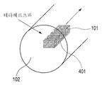
도1은, 본 발명에 따른 도파로의 개략도이다. 도1에 도시된 것처럼, 본 발명의 도파로(100)는, 단일선(101)과, 단일선을 덮는 유전체 부재(102)로 구성한다. 또한, 유전체 부재(102)는, 틈부(103)를 갖고 있다.1 is a schematic diagram of a waveguide according to the present invention. As shown in Fig. 1, the
단일선(101)은, 도체로 구성하는 단일의 도선이다. 도1에서는, 단일선(101)은, 원기둥 모양이지만, 그 단일선의 모양은 이 모양에 한정하는 것이 아니다. 예를 들면, 단일선(101)은 다각형상이어도 좋다.The
유전체 부재(102)는, 유전체로 구성한다. 본 발명에서는, 유전체 부재(102)에 사용된 유전체재료는, 사용하는 전자파에 대하여, 투명한 특성인 것이 바람직하다. 도1에서는, 유전체 부재(102)는, 원기둥 모양이지만, 그 모양은 이 모양에 한정하는 것이 아니다. 예를 들면, 유전체 부재(102)의 모야은 다각형상이어도 되고, 기판형이어도 된다. 또한, 유전체 부재(102)의 사이즈는, 도파로(100)를 통해 전파하는 전자파가, 도파로(100) 안에 분포되는 정도인 것이 바람직하다. 이것은, 도파로(100)를 통해 전파된 전파하는 전자파에 대한, 외부의 영향을 억제하기 위함이다. 단일선(101)을 통해 전파하는 전자파의 전자계 분포는, 동축 도파로에 같은 전 자계 분포이라는 것이 알려져 있다. 예를 들면, 도1과 같이, 원기둥 모양의 유전체 부재(102)를 사용했을 경우를 생각한다. 계산에 의하면, 단일선(101)과 유전체 부재(102) 사이의 계면으로부터, 유전체 부재(102)의 외주면까지의 거리가, 반파장 이상이면, 도파로(100)를 통해 전파하는 전자파의 전자계는, 유전체 부재(102) 안에 분포된다. 또한, 도파로(100)를 통해 전파하는 전자파가, 임의의 주파수영역을 갖는 경우를 생각한다. 이 경우, 단일선(101)과 유전체 부재(102) 사이의 계면으로부터, 유전체 부재(102)의 외주면까지의 거리가, 전자파가 점유하는 주파수영역 중, 최저주파수의 파장에 대하여, 파장 반파장 이상 확보한다.The
(유전체 부재 내의 틈)(Gap in Dielectric Member)
도1과 같이, 본 발명의 도파로(100)는, 유전체 부재(102)의 일부에, 틈부(103)를 갖고 있다. 도1에서는, 틈부(103)의 유전체 피막이 제거되고, 단일선(101)이 노출되어 있다. 유전체 부재(102)와 틈부(103)의 굴절률이 다른 경우, 도파로(100)를 통해 전파하는 전자파의 전파 상태는, 틈부(103)에 있어서 변화된다. 이렇게, 틈부(103)에 있어서의, 굴절률 차이에 기인한, 전자파의 전파 상태의 변화를 이용함으로써, 상기 전자파의 일부의 주파수성분을 선택적으로 제거하여 투과한다고 하는 신호 제어가 가능하게 된다. 도1에서는, 유전체 부재(102)의 일부에, 틈부(103)를 설치하는 구성이지만, 그 틈부를 형성하는 방법은 유전체를 제거하는 방법에 한정하는 것이 아니다. 전자파의 전파 경로에, 굴절률이 변화되는 영역이 존재하는 것이 필요할 뿐이다. 그래서, 예를 들면, 유전체 부재(102)와 다른 물질을 틈부(103)에 충전하는 구성도 적용하여도 된다. 또한, 도15와 같이, 틈 부(103)의 유전체를 모두 제거하지 않고, 일부를 남기는 구성을 적용하여도 된다.이러한 경우에서도, 틈부(103)에 있어서의 평균 굴절률이 변화되어서, 전자파의 전파 상태를 변화시킬 수 있다.As shown in FIG. 1, the
또한, 도1에 있어서, 틈부(103)를 거쳐서 서로 대향 배치되는 유전체 부재(102)의 단면은, 단일선(101)의 길이 방향에 대하여, 수직하게 형성되어 있다. 그러나, 상기 틈부 내의 구성은, 이 배치에 한정하는 것이 아니다. 예를 들면, 도16과 같이, 단일선(101)의 길이 방향에 대하여, 유전체 부재(102)의 단면이 경사진 구성을 적용하여도 된다. 또한, 도17과 같이, 유전체 부재(102)의 단면이 테이퍼형이어도 된다. 또한, 상술한 것과 같은 유전체 부재(102)의 단면은, 평면형이지만, 그 단면의 일부 또는 전부가, 구면형이어도 좋고, 요철형 또는 다각형이어도 된다. 또한, 도18과 같이, 나선 모양으로 유전체를 제거해도 좋다. 또한, 나선 모양으로 제거한 부분의 간격도 일정하지 않아도 되지만, 부분적으로 불규칙이거나 일정한 비율로 변화되어도 좋다.In Fig. 1, the end faces of the
또한, 틈부는 도파로중에 규칙적으로 배치되는 것이 바람직하다. 그렇지만, 틈 전부가 규칙적으로 배치될 필요는 없다. 틈의 일부가 규칙적으로 배치된 상태는 효과적이다. 또한, 틈이 규칙적으로 배치되어 있는 상태에서, 의도적으로 그 배치의 규칙성을 방해하도록 틈부를 구성해도 좋다. 이에 따라, 파장 선택성을 얻을 수 있다. 주기적 배치는, 틈이 특정 파장장의 간격으로 배치되어 있는 배치를 의미한다. 자기상사(self-similar) 배치는, 도파로의 단면에서 보았을 때, 그 단면에 대해 좌우 대칭인 구조를 의미한다.In addition, the gap portion is preferably arranged regularly in the waveguide. However, not all gaps need to be regularly arranged. The regular arrangement of some of the gaps is effective. In the state where the gaps are regularly arranged, the gaps may be configured to intentionally interfere with the regularity of the arrangement. Thereby, wavelength selectivity can be obtained. The periodic arrangement means an arrangement in which gaps are arranged at intervals of a specific wavelength field. Self-similar arrangement means a structure that is symmetrical with respect to the cross section when viewed from the cross section of the waveguide.
(센서 장치의 구성)(Configuration of Sensor Unit)
도2는, 전술한 도파로를, 검체의 물성을 측정하는 센서 장치에 응용했을 경우의, 개략도다. 도2와 같이, 본 발명의 장치는, 발생부(201), 도파로(100), 검출부(202), 비교부(203), 기억부(204) 및 제시부(205)로 구성한다.Fig. 2 is a schematic diagram when the waveguide described above is applied to a sensor device for measuring physical properties of a specimen. As shown in Fig. 2, the apparatus of the present invention includes a
발생부(201)는, 본 장치에서 사용하는 고주파 전자파, 예를 들면 테,라헤르츠파를 발생하여, 도파로(100)에 결합시켜 전파시킬 수 있는 기능을 가진다. 발생부(201)는, 도파로(100)와 일체로 되도록 구성해도 좋고, 또는 도파로(100)의 외부에서 고주파 전자파를 발생시켜 도파로(100)에 결합시키도록 구성해도 좋다.The generating
(센서 장치의 발생 수단과 결합 수단)(Generation means and coupling means of the sensor device)
발생부(201)는, 고주파 전자파를 발생시켜 공간에 전파시키는 수단과, 도파로(100)에의 결합 수단으로 구성할 경우를 생각한다. 이 경우, 예를 들면, 도4와 같이, 결합 수단은, 도파로(100)를 구성하는 단일선(101)의 일부에, 그레이팅 구조(401)로서 구성된다. 이때, 결합 수단은, 외부로부터 전파된 고주파 전자파 중, 그레이팅의 주기에 대응한 파장을, 선택적으로 결합한다. 이 구조의 제작 방법은, 예를 들면 그레이팅이 내부에 형성된 단일선(101)을, 액상의 유전체 부재(102)로 채워진 형태에 삽입하고, 열에 의해 유전체 부재(102)를 경화시킨다고 한 방법이 생각될 수 있다. 그렇지만, 이 구조의 제작 방법은, 이 방법에 한정하는 것이 아니고, 기지의 프로세스 기술을 사용할 수 있다.The
또한, 도5와 같이, 결합 수단으로서, 도파로(100)를 구성하는 단일선(101)에 대하여, 한층 더 도체를 직교 배치하는 크로스 와이어 구조(501)를 사용하는 방법 이 있다. 이 경우, 상기 "Nature", vol.432, p376-379, 2004에 기재된 경우와 마찬가지로, 외부로부터 전파된 고주파 전자파를, 크로스 와이어 구조(501)에 결합시킨다. 이러한 구조의 제작 방법으로서는, 예를 들면, 단일선(101)을 포함하는 유전체 부재(102)의 외주면 위에, 크로스 와이어 구조(501)를 패터닝 하는 방법이 있다. 그렇지만, 이 구조의 제작 방법은 상기 제작 방법에 한정되는 것이 아니고, 기지의 프로세스 기술도 사용할 수 있다. 또한, 도5의 크로스 와이어 구조(501)는, 유전체 부재(102)의 외주면 위에 제작되어 있지만, 유전체 부재(102) 내부에 매립되어서 있어도 된다.In addition, as shown in Fig. 5, there is a method of using a
또한, 발생부(201)는, 고주파 전자파를 발생시키는 수단과, 도파로(100)에의 결합 수단을 일체화해서 구성할 수도 있다. 이 경우, 예를 들면, 도6과 같이, 발생부(201)로서, 광전도 스위치 구조(601)를 사용하는 방식이 있다. 광전도 스위치 구조(601)에는, 단일선(101)으로부터 추출된 도전부재와, 어떤 미소한 틈에 분리된 전극으로부터 추출된 도전부재가 구비된다. 한층 더, 광전도 스위치 구조(601)는, 상기 단일선(101)으로부터 추출된 전극과 유전체 부재(102)의 일부에 형성된 전극(602) 사이의 틈에, 캐리어의 라이프 타임이 짧은 반도체(예를 들면, 저온성장 갈륨 비소:LT-GaAs)를 밀착시키도록 구성된다. 광전도 스위치 구조(601)의 동작은, 상기한 틈부에 전계를 인가한 상태에서, 초단 펄스 레이저 빔을 사용해서 외부에서 광학적으로 게이트 함으로써, 고주파 전자파를 발생한다. 광전도 스위치 구조(601)에서 발생한 고주파 전자파는, 단일선(101)과 유전체 부재(102)로 구성되는 도파로(100)에 결합해 전파된다. 이것들의 전극은, 기지의 프로세스 기술에 의해 패터닝 된다. 또한, 광전도 스위치 구조(601)를 구성하는 반도체는, 예를 들면, 박막화하고, 유전체 부재(102)에 붙일 수 있다. 한편, 광전도 스위치 구조(601)의 제작 방법은, 이 방법에 한정되는 것은 아니다. 또한, 도6에 있어서, 광전도 스위치 구조(601)는, 단일선(101)과 유전체 부재(102)로 구성된 도파로의 단면에 형성되어 있지만, 이 구성에 한정하는 것이 아니다. 예를 들면, 유전체 부재(102)의 내부, 또는 외주면 위에 형성 되어 있어도 된다. 또한, 전극(602)은, 단일선(101)에 대하여, 동심원 모양으로 패터닝 되어 있다. 이것은, 단일선(101)과 유전체 부재(102)로 구성된 도파로(100)의 전파 모드가, 동축 케이블과 같은 TEM모드인 것에 착안하여서, 보다 결합 상태를 양호하게 유지하기 위해서, 고주파 전자파 발생측의 구조를 동축구조로 형성되기 때문이다. 그러나, 중요한 것은, 광전도 스위치 구조(601)를 구성하는 도체들 사이의 틈에 전계가 인가될 필요만 있을 것이다는 것이다. 그래서, 당연히 광전도 스위치 구조(601)는 이 동축 구조에 한정하는 것이 아니다.The
또한, 도7과 같이, 발생부(201)로서, 전자파 이득구조(701)을 사용하는 방식이 있다. 전자파 이득구조(701)는, 어떤 미소 간격으로 서로 분리된, 단일선(101)으로부터 인출된 전극과, 유전체 부재(102)의 일부에 형성된 전극(702)에 대하여, 고주파 전자파 영역에 이득이 있는 전자파 이득물질을 밀착시킨 구조다. 전자파 이득물질은, 예를 들면 공명터널다이오드(RTD)나 Gunn 다이오드 등으로 대표되는 전자파 이득을 얻을 수 있는 반도체소자다. 또한, 양자 캐스케이드 레이저와 같은, 고주파 전자파 발진 소자이어도 좋다. 상기한 바와 같이, 이 전자파 이득물질은, 고주파 전자파 중, 원하는 주파수대에서 이득을 얻도록 설계되어 있다. 이에 따라 서, 전자파 이득구조(701)에 바이어스를 인가함으로써, 고주파 전자파를 발생한다. 그리고, 전자파 이득구조(701)에서 발생한 고주파 전자파는, 단일선(101)과 유전체 부재(102)로 구성된 도파로(100)에 결합해 전파한다. 이것들의 전극은, 기지의 프로세스 기술에 의해 패터닝 된다. 한편, 도7에 있어서, 전자파 이득구조(701)는, 단일선(101)과 유전체 부재(102)로 구성된 도파로(100)의 단면에 형성되어 있지만, 이 구성에 한정하는 것이 아니다. 예를 들면, 전자파 이득구조(701)는, 유전체 부재(102)의 내부 또는 외주면 위에 형성되어 있어도 된다. 또한, 전극(702)은, 단일선(101)에 대하여, 동심원 모양으로 패터닝 되어 있다. 이것은, 단일선(101)과 유전체 부재(102)로 구성된 도파로(100)의 전파 모드가, 동축케이블과 같은 TEM모드인 것에 착안하여서, 보다 결합 상태를 양호하게 유지하기 위해서, 고주파 전자파발생측의 구조를 동축 구조로 형성되기 때문이다. 그러나, 중요한 것은, 전자파 이득구조(701)를 구성하는 도체들의 틈에 바이어스가 인가될 필요가 있을 뿐이다는 것이다. 그래서, 당연히, 이 전자파 이득구조(701)는 이 동축 구조에 한정하는 것이 아니다.As shown in Fig. 7, there is a system using the
또한, 도8과 같이, 발생부(201)로서, 도파로 변환구조(801)를 사용하는 방식이 있다. 도파로 변환구조(801)는, 다른 고주파 모듈을 전파하는 고주파 전자파를, 단일선(101)과 유전체 부재(102)로 구성된 도파로에 결합하는 구성이다. 도8은, 이 구성의 평면도, 단면도 및 측면도를 나타낸 것이다. 도8과 같이, 도파로 변환구조(801)는, 유전체 부재(102), 제1도체(802)와 제2도체(803)로 구성되는 전송선로(마이크로스트립 선로)에 대하여, 제1도체(802)와 제2도체(803)의 사이에, 단일 선(101)이 삽입되는 구조다. 이러한 구조를 가짐으로써, 고주파 모듈 내에서 전파하는 고주파 전자파는, 도파로 변환구조(801)에 있어서, 단일선(101)과 유전체 부재(102)로 구성된 도파로에 결합하여, 전파한다. 도파로 변환구조(801)를 구성하는 전송선로 구조는, 도8에 나타나 있는 바와 같은, 마이크로스트립 선로에 한정하는 것이 아니다. 예를 들면, 코플래너 도파로 등, 고주파 전자파신호를 전파하기 위해서 사용하는 것 같은 전송선로구조를 이용할 수 있다. 또한, 도파관과 동축 구조 등, 입체적인 도파로 구조에도 적용할 수 있다. 또한, 도파로 변환구조(801)에 있어서, 임피던스의 부정합을 경감하고, 고주파 전자파신호의 결합 상태를 향상시키기 위해서, 단일선(101)과 유전체 부재(102)의 형상이 부분적으로 변화되는 구성도 생각할 수 있다. 예를 들면, 도파로 변환구조(801)의 단부에 있어서, 단일선(101)과 유전체 부재(102)의 사이즈를 부분적으로 굵게 하는 것이나, 가늘게 하는 것, 또는 테이퍼 형상을 사용하는 것 등을 생각할 수 있다.As shown in Fig. 8, there is a system in which the
상기 발생부(201)의 구성은 이들 구성에 한정하는 것이 아니고, 발생부(201)에서 발생한 고주파 전자파가 도파로(100)에 결합하여, 전파하는 어떠한 구성도 사용되어도 된다. 예를 들면, 안테나를 거쳐서, 발생부(201)에서 발생한 고주파 전자파를, 도파로(100)에 결합시키는 방법도 있다.The configuration of the
도2에 있어서, 검출부(202)는, 도파로(100)를 통해 전파된 고주파 전자파를, 검출하는 기능을 가진다. 검출부(202)의 구조는, 발생부(201)와 같은 구조를 사용할 수 있다. 그렇지만, 검출부(202)의 구조는, 이것들의 구조에 한정하는 것이 아니고, 도파로(100)를 통해 전파하는 고주파 전자파를 검출할 목적을 달성할 수 있 으면 좋다.In FIG. 2, the
(센서 장치의 기억 수단과 비교 수단)(Memory means and comparison means of the sensor device)
기억부(204)에는, 검체의 물성을 측정하는 센서 장치에 있어서, 검체의 참조 정보가 미리 기억되어 있다. 기억부(204)에 기억된 검체의 참조 정보는, 예를 들면 굴절률이나 감쇠 등의 정보를 포함한다. 그렇지만, 상기 참조 정보는, 이것에 한정하는 것이 아니고, 검체의 물성을 특징으로 하는 어떠한 정보도 기억되어도 된다. 기억부(204)는, 기억부(204)에 기억된 검체의 참조 정보를, 연속적으로 갱신하는 기능을 갖고 있어도 된다. 예를 들면, 현재, 측정하고 있는 검체의 물성정보를, 검체의 참조 정보로서 기억할 수도 있다.In the
비교부(203)는, 검출부(202)에서 검출된 검체의 정보와, 기억부(204)에 기억되어 있는 참조 정보를 비교하는 부분이다. 비교부(203)는, 검출부(202)에서 검출된 검체의 정보를, 기억부(204)에 기억되어 있는 참조 정보에 대응한 형태에 처리하는 기능을 가진다. 예를 들면, 시계열 정보를, 스펙트럼 정보로 변환한다. 그렇지만, 처리 형태는, 이 형태에 한정하는 것이 아니다. 예를 들면, 비교부(203)는, 지연 정보를 취득하거나, 복소 유전율을 산출하거나 하는 기능을 갖는다. 본질적인 것은, 기억부(204)에 기억되어 있는 검체의 참조 정보와 비교할 수 있는 형태이어도 된다는 것이다.The
제시부(205)는, 비교부(203)에서 비교한 결과를 제시하는 부분이다. 제시 방법으로서는, 디스플레이에 표시하는 방법을 생각할 수 있다. 그렇지만, 이 제시 방법은, 이 방법에 한정하는 것이 아니다. 예를 들면, 검사 물질의 유무만을 알 경 우, 빛의 점멸과 소리, 또는 촉각 제시장치 등을 사용할 수 있다. 본질적인 것은, 어떠한 방법으로, 사용자에게 측정 결과를 알릴 수 있으면 좋다.The
(센서 장치의 동작 설명)(Explanation of operation of sensor unit)
다음에, 본 발명에 있어서의 검체의 물성을 측정하는 센서 장치의 동작을 설명한다. 우선, 본 발명의 검체의 물성을 측정하는 센서 장치에서는, 도파로(100)의 틈에 검체를 삽입한다. 도파로(100)를 통해 전파하는 고주파 전자파는, 도파로(100)의 틈부(103)에 있어서, 검체와 상호 작용한다. 그 결과, 도파로(100)를 통해 전파하는 고주파 전자파의 전파 상태는, 검체의 존재에 의해 변화된다. 이 고주파 전자파의 전파 상태의 변화는, 검체의 물성에 따라 다르다. 이러한 전파 상태가 변화된 고주파 전자파는, 검출부(202)에 의해 검출된다.Next, operation | movement of the sensor apparatus which measures the physical property of the sample in this invention is demonstrated. First, in the sensor apparatus which measures the physical property of the sample of this invention, a sample is inserted in the clearance gap of the
도1에 있어서, 도파로(100)의 유전체 부재(102)에 틈부(103)가 존재할 경우, 틈부(103)에는, 용량성분이 부가된다. 이 용량성분은, 틈부(103)에 삽입된 검체의 물성에 따라 변화된다. 그 때문에, 이 틈부(103)에 검체를 삽입했을 경우, 도3과 같이, 주파수특성이나 전파 지연특성이 변화된다. 여기에서, 도3은, 틈부(103)에, 검체를 삽입했을 경우의, 전반특성변화를 나타낸 이미지 그래프이다. 여기에서 나타낸 도면은, 단지 이미지 그래프이며, 실제의 전반특성변화는, 검체가 갖는 분산 특성, 감쇠특성, 흡수 특성에 의해, 보다 복잡하게 변화된다. 도3의 주파수특성에 볼 수 있듯이, 도파로(100)의 틈부(103)에 의해, 도파로(100)는, 저주파수측의 신호를 감쇠시키는 하이패스 필터와 같이 기능하는 것이 예상된다. 이 때, 틈부(103)에 있는 검체의 물성에 의해, 하이패스 필터의 컷오프 주파수가 변화된다. 또한, 도3의 전파 지연특성으로부터 볼 수 있듯이, 검체의 물성에 따라, 지연시간이 변화된다. 비교부(203)에서는, 우선, 틈부(103)에 검체를 삽입함으로써 변화된, 주파수특성과 전파 지연특성의 변화에 의해, 검체의 물성을 취득한다.In FIG. 1, when the
검체의 물성 정보는, 미리 기억부(204)에 기억되어 있다. 이에 따라서, 기억부(204)에 기억되어 있는 물성정보와, 비교부(203)에 있어서 상기 취득된 물성정보를 비교함으로써, 검체의 분석과 분류를 행할 수 있다. 본 발명의 검체의 물성을 측정하는 센서 장치에서는, 기억부(204)에 물성정보를 추가할 수 있다. 예를 들면, 미리 물성이 기지인 검체를, 본 발명의 검체의 물성을 측정하는 센서 장치에 의해 측정하고, 그 측정 결과를 기억부(204)에 추가한다. 상기 측정 결과의 기억은, 장치고유의 측정 결과의 변동을 억제하는데 효과적이다.The physical property information of the specimen is stored in the
이들의 비교 결과는, 제시부(205)에 의해, 측정자에게 제시된다.These comparison results are presented to the measurer by the
이상에서 설명한 바와 같이, 본 발명의 도파로에서는, 도파로를 통해 전파하는 전자파의 전파 상태가 변화되어서, 쉽게 기능성을 도파로에 부가할 수 있다. 또한, 종래의 전송선로기술에서는, 손실과 분산 특성의 문제가 되었다. 따라서, 규모가 큰 회로를 형성하려고 했을 경우, 신호 열화를 초래하여서, 테라헤르츠파 신호의 제어가 어렵게 되었다. 본 발명의 도파로는, 상기한 바와 같이, 저손실 및 저분산 특성을 나타내는 단일선의 도파로에 대하여, 유전체 부재에 의해 기능성을 부가하는 구성이다. 이에 따라서, 본 발명의 도파로에서는, 신호 열화의 영향을 최소로 유지하면서, 신호 제어를 행할 수 있다. 이 때문에, 용이하게, 대규모 회로 및 장치에 적응할 수 있다.As described above, in the waveguide of the present invention, the propagation state of electromagnetic waves propagating through the waveguide is changed, so that functionality can be easily added to the waveguide. In addition, in the conventional transmission line technology, problems of loss and dispersion characteristics have arisen. Therefore, when attempting to form a large-scale circuit, signal degradation occurs, making it difficult to control the terahertz wave signal. As described above, the waveguide of the present invention is configured to add functionality to the waveguide of a single line showing low loss and low dispersion characteristics by the dielectric member. Accordingly, in the waveguide of the present invention, signal control can be performed while keeping the influence of signal degradation to a minimum. For this reason, it is easy to adapt to a large scale circuit and an apparatus.
또한, 본 발명의 검체의 물성을 측정하는 센서 장치는, 상기 도파로의 틈부분에 검체를 삽입하고, 전자파와의 상호작용의 변화를 검출하는 구성이다. 그래서, 종래의 파이버 도파로에 필요한, 어떤 틈을 거쳐서 파이버 도파로를 대향배치시키는 외부기구가 필요 없어서, 본 발명의 장치구성이 간단해진다. 또한, 종래의 전송선로기술을 사용한 검사장치에서는, 손실, 분산이 비교적 크기 때문에, 검사 부분과 검출 부분을 가능한 한 가까이 하는 것이 기대되었다. 그러나, 본 발명의 검체의 물성을 측정하는 센서 장치는, 저손실 및 저분산 도파로 구조에, 검사 부분을 형성하는 구성이어서, 검사 부분과 검출 부분을 떨어지게 할 수 있다. 그에 따라서, 예를 들면, 위험 구역에서의 검사 작업을 행할 경우, 검사 부분만을 위험 구역에 갖고 들어가고, 안전 구역에서 검출 작업을 행할 수 있다. 이것에 의해, 안전성이 향상한다고 하는 효과가 있다. 또한, 검사 부분을 분리할 수 있으므로, 밀폐 공간(예를 들면, 쳄버내 등)에서의 검사 작업이나 용액중에서의 검사 작업 등도 가능하게 된다. 이것에 의해, 검사 작업의 적용 가능 범위가 넓어진다고 하는 효과가 있다.Moreover, the sensor apparatus which measures the physical property of the sample of this invention is a structure which inserts a sample into the clearance gap of the said waveguide, and detects the change of interaction with an electromagnetic wave. Therefore, no external mechanism for opposing the fiber waveguides through any gap necessary for the conventional fiber waveguides is required, which simplifies the device configuration of the present invention. In addition, in the inspection apparatus using the conventional transmission line technology, since the loss and dispersion are relatively large, it was expected to bring the inspection portion and the detection portion as close as possible. However, the sensor device for measuring the physical properties of the specimen of the present invention is configured to form an inspection portion in the low loss and low dispersion waveguide structure, so that the inspection portion and the detection portion can be separated. Therefore, for example, when performing inspection work in a danger zone, only an inspection part can be carried in a danger zone, and a detection operation can be performed in a safety zone. This has the effect of improving safety. In addition, since the inspection part can be separated, inspection work in a closed space (for example, in a chamber, etc.), inspection work in a solution, and the like become possible. This has the effect of widening the applicable range of the inspection work.
[실시 예][Example]
이하에, 보다 구체적인 실시 예에 대해서, 도면을 참조해서 설명한다.EMBODIMENT OF THE INVENTION Below, a more specific Example is described with reference to drawings.
(실시 예1)(Example 1)
본 실시예에서는, 도파로의 틈부가, 주기적으로 배치하고 있는 구성 예에 대해서 서술한다. 도9와 같이, 본 실시예의 도파로는, 단일선(101), 유전체 부 재(102) 및 틈부(901)로 구성된다. 도9와 같이, 틈부(901)에는 틈이 주기적으로 배치되어 있다. 이러한 배치에 의해, 틈부(901)에 있어서, 유전체 부재(102)를 구성하는 물질과 틈부(901)의 굴절률이 주기적으로 변화되는 구성이 된다. 그 결과, 본 실시예의 도파로는, 틈부(901)에 있어서, 포토닉 밴드갭에 기인하는 파장 선택성을 가진다.In this embodiment, a configuration example in which the gap portion of the waveguide is periodically arranged will be described. As shown in Fig. 9, the waveguide of the present embodiment is composed of a
본 실시예의, 검체의 물성을 측정하는 센서 장치에서는, 이 파장 선택성의 변화에 의거하여, 검체의 물성을 검출하는 것이다.In the sensor apparatus which measures the physical property of a sample of a present Example, the physical property of a sample is detected based on this change of wavelength selectivity.
본 실시예에서는, 단일선(101)으로서 금선을 사용한다. 유전체 부재(102)로서 고저항 실리콘(유전율: 11.4, 도전율: 0.01S/m)을 사용한다. 그렇지만, 단일선(101)과 유전체 부재(102)의 재료는, 이것들의 재료에 한정하는 것이 아니다. 단일선(101)은, 도체이면 된다. 그래서, 백금선과 동선을 사용하여도 된다. 유전체 부재(102)로서는, 유전체 재료 중 임의의 재료를 사용하여도 되지만, 바람직하게는, 사용하는 고주파 전자파에 대하여, 분산 및 흡수가 낮은 특성을 갖는 유전체 재료를 사용한다. 구체적으로는, 벤조시클로부텐, 폴리이미드, 폴리실란 등을 유전체 부재(102)의 유전체 재료로서 사용한다. 또한, 반도체 재료 등도 유전체 재료로서 사용하여도 된다. 본 실시예에서는, 단일선(101)의 형상은, 도9와 같이, 직경 10㎛의 원기둥 모양을 사용한다. 그렇지만, 단일선(101)의 형상은, 이 형상에 한정하는 것이 아니다. 예를 들면, 단일선(101)의 형상은, 다각형상이어도 된다. 또한, 도9와 같이, 한변이 200㎛인 4각 기둥형상을 유전체 부재(102)의 형상으로서 사용한다. 그렇지만, 유전체 부재(102)의 형상은, 이 형상에 한정되지 않는다. 예를 들 면, 원기둥형상과 다각형상을 사용하여도 된다. 유전체 부재(102)의 한변의 길이는, 이 값에 한정하는 것이 아니다. 이 값은, 사용하는 고주파 전자파의 파장에 따라 변화된다.In this embodiment, a gold wire is used as the
도9와 같이, 유전체 부재(102)에는, 틈이 주기적으로 배치되어 있다.틈부(901)는, 폭 50㎛의 틈을 50㎛간격으로 주기적으로 배치되어 있다. 이것들의 틈은, 유전체 부재(102)를 구성하는 재료를 제거해서 구성된다. 이것들의 틈은, 도파로(100)를 통해 전파하는 전자파의 실효파장에 대응한 파장 오더의 간격으로 주기적으로 배치되는 것이 바람직하다.As shown in Fig. 9, gaps are periodically arranged in the
본 실시예에서 사용하는 도파로는, 예를 들면 아래와 같이 제작된다. 우선, 두께 100㎛의 고저항 실리콘 기판에, 단일선(101)을 유지하기 위한 홈을 제작한다. 다음에, 상기 단일선(101)을 유지하기 위한 홈에 대하여, 수직하게 교차하도록, 50㎛ x 200㎛ 크기의 관통구멍을 주기적으로 제작한다. 이 관통구멍은, 틈부(901)에 해당한다. 이것들의 패턴은, 예를 들면 일반적인 포토리소그래피 기술과 드라이에칭 기술 등으로 제작한다. 이러한 종류의 기판은, 2장 제작한다. 그 후, 기판의 홈 부분에 단일선(101)을 배치하고, 이미 한쪽의 실리콘 기판을, 홈 부분을 내측으로 해서 밀착시킨다. 이 경우에, 이것들의 실리콘 기판의 계면에는, 수지접착제가 도포되어 있어, 기판을 서로 고정한다. 여기에서, 수지접착제는, 사용하는 고주파 전자파에 대하여, 분산 및 흡수가 낮은 특성을 갖는 것을 사용한다. 실리콘 기판을 고정 후, 기판은, 관통구멍을 따라 절단되어, 도파로가 형성된다. 제작 방법은, 단지 일례이며, 본 발명의 도파로의 제조방법은 이 방법에 한정하는 것이 아니다. 보 통 사용된 프로세스 기술은, 도파로의 제조방법으로서 사용될 수 있다.For example, the waveguide used in this embodiment is manufactured as follows. First, grooves for holding the
도10은, 본 실시예의 도파로를, 검체의 물성을 측정하는 센서 장치에 전용했을 경우의 동작을 나타낸 그래프이다. 도10은, 전자계 시뮬레이터에 의해 계산한 계산 결과다.Fig. 10 is a graph showing the operation when the waveguide of the present embodiment is converted to a sensor device for measuring the physical properties of the specimen. 10 is a calculation result calculated by the electromagnetic field simulator.
도10에 있어서, 파선은, 본 실시예의 도파로의 틈부(901)에, 검체가 없는 상태의, 전반특성을 나타낸다. 또한, 실선은, 본 실시예의 도파로의 틈부(901)에, 검체로서, DNA(유전율: 4.0, 유전 손실 탄젠트(tanδ):0.01)를 삽입했을 경우의, 전반특성을 나타낸다. 도10과 같이, 틈부(901)의 틈이, 주기적인 배치를 갖는 것에 의해, 파장이 투과하지 않는 영역(전자파의 투과 레벨이 거의 0이 되는 파장영역)이 제시된다. 또한, 틈부(901)에 검체를 삽입하면, 검체가 틈부(901)에 삽입되지 않는 경우와 비교하여, 주파수특성이 저주파수측으로 시프트한다는 것을 안다. 한층 더, 투과 강도도 변화되고 있는 것을 도면으로부터 안다. 또한, DNA에 있어서, 단일쇄와 이중쇄 사이에서 유전율이 다르기 때문에, 그 차이를 검출할 수 있다. 이 정보로부터, 검체의 물성을 취득한다. 또한, 도면에 나타내지 않았지만, 도파로를 통해 전파하는 고주파 전자파의 지연 정보를 사용해도 된다. 검체의 물성을 취득할 경우, 이 종류들의 정보를 모두 사용해도 되거나, 이 종류들의 정보 중 어느 하나를 선택하여도 된다. 또한, 이들 종류의 정보를 조합하여도 된다. 또한, DNA뿐만아니라, 단백질과 아미노산 등의 생체분자에 있어서, 검체 자체의 구조변화와 특성변화를 검출하는 것도 가능하다.In FIG. 10, the broken line shows the propagation characteristic in the state where there is no sample in the
이렇게 하여 얻어진 검체의 물성과 관련지어, 기억부(204)에 기억되어 있는 정보와 비교함으로써, 검체의 분류와 분석을 한다.In connection with the physical properties of the specimen thus obtained, the classification and analysis of the specimen are performed by comparing with the information stored in the
본 실시예에서는, 도파로의 틈부(901)는 주기적으로 배치되어 있다. 일반적으로, 이러한 구조는, 높은 Q값을 나타내는 것이 알려져 있기 때문에 검출 감도가 향상한다. 즉, 본 실시예의 검체의 물성을 측정하는 센서 장치는, 고감도 측정을 가능하게 하는 효과뿐만 아니라, 미량의 검체에 대해서도 우수한 감도로 측정을 가능하게 하는 효과도 갖는다.In this embodiment, the
(실시 예2)(Example 2)
본 실시예에서는, 도파로의 틈부가, 자기상사적으로 배치하고 있는 구성 예에 대해서 서술한다. 도11과 같이, 본 실시예의 도파로는, 단일선(101), 유전체 부재(102) 및 틈부(1101)로 구성된다. 도면과 같이, 틈부(1101)는 자기상사적으로 배치되어 있다. 본 실시예의 경우, 틈부(1101)에 해당하는 영역에 유전체 부재(102)에 대해서, 3등분하고, 중심의 유전체를 남긴다(이것을 1스테이지라고 부른다). 중앙의 유전체 양측에 유전체마다 같은 작업을 3회 반복하여서, 구조(3스테이지의 포토닉 프랙탈 구조)를 얻는다. 이러한 배치에 의해, 틈부(1101)에 있어서, 유전체 부재(102)를 구성하는 물질과 틈부(1101)의 굴절률이, 자기상사적으로 변화되는 구성이 된다. 그 결과, 본 실시예의 도파로는, 파장 선택성을 가진다.In the present embodiment, a configuration example in which the gap portion of the waveguide is arranged self-similarly will be described. As shown in Fig. 11, the waveguide of the present embodiment is composed of a
본 실시예의 검체의 물성을 측정하는 센서 장치에서는, 이 파장 선택성의 변화에 의해, 검체의 물성을 검출한다.In the sensor apparatus which measures the physical property of the sample of a present Example, the physical property of a sample is detected by this change of wavelength selectivity.
본 실시예에서는, 단일선(101)으로서 금선을 사용한다. 유전체 부재(102)로서 고저항 실리콘(유전율: 11.4, 도전율: 0.01S/m)을 사용한다. 본 실시예에서는, 단일선(101)의 형상은, 도11과 같이, 직경 10㎛의 원기둥형상을 사용한다. 또한, 유전체 부재(102)의 형상은, 도11과 같이, 한변이 200㎛인 4각 기둥형상을 사용한다. 그렇지만, 실시 예1과 마찬가지로, 단일선(101) 및 유전체 부재(102)의 형상은, 이것들의 재료와 형상에 한정되는 것은 아니다. 도11과 같이, 유전체 부재(102)에는, 틈부(901)가 자기상사적으로 배치되어 있다. 예를 들면, 측정에 사용하는 고주파 전자파로서, 1THz정도의 전자파를 고려한 경우를 생각한다. 이 때, 틈부(1101)로서, 사용하는 전자파의 파장 오더의 영역에 상기한 3스테이지의 포토닉 프랙탈 구조를 배치한다. 이것들의 틈은, 유전체 부재(102)를 구성하는 재료를 제거해서 구성된다. 여기에서, 파장 오더는, 도파로(100)를 통해 전파된 전자파의 실효파장 중, 약 1파장정도를 말한다.In this embodiment, a gold wire is used as the
본 실시예에 있어서, 본 실시예의 도파로의 제작 방법은, 실시 예1에 나타낸 것과 같다.In this embodiment, the waveguide manufacturing method of the present embodiment is the same as that shown in the first embodiment.
본 실시예와 같이 자기상사적인 도파로 구성을 갖는 경우, 도파로의 전반특성은, 어떤 고유의 주파수에 있어서, 국재모드를 갖는다. 그리고, 이 도파로를, 검체의 물성을 측정하는 센서 장치에 전용했을 경우를 생각한다. 실시 예1의 경우와 마찬가지로, 도파로의 틈부(1101)에 검체를 삽입하면, 고주파 전자파의 전파 상태가 변화되어서, 주파수특성이 변화된다. 구체적으로는, 국재모드가 저역측으로 쉬프트한다. 한층 더, 실시 예1의 경우와 마찬가지로, 투과 강도도 변화된다. 이들 종류의 정보로부터, 검체의 물성을 취득한다. 또한, 도파로를 통해 전파하는 고주파 전자파의 지연 정보를 사용해도 된다. 검체의 물성을 취득할 경우, 이들 종류의 정보를 모두 사용해도 되거나, 어느 하나의 정보를 선택하여도 된다. 또한, 이들 종류의 정보를 조합하여도 된다. 또한, 실시 예1의 경우와 마찬가지로, 본 실시예의 검체의 물성을 측정하는 센서 장치에 있어서도, 검체 자체의 구조변화와 특성변화를 검출하는 것도 가능하다.In the case where the waveguide configuration is self-similar as in the present embodiment, the propagation characteristics of the waveguide have a local mode at a specific frequency. The case where the waveguide is transferred to a sensor device for measuring the physical properties of the specimen is considered. As in the case of the first embodiment, when the specimen is inserted into the
이렇게 하여 얻어진 검체의 물성과 상기 기억부(204)에 기억되어 있는 정보를 비교함으로써, 검체의 분류와 분석을 행한다.By comparing the physical properties of the specimen thus obtained with the information stored in the
실시 예1의 경우와 마찬가지로, 본 실시예와 같이 형성된 자기상사 구조는, 높은 Q값을 나타내는 것이 일반적으로 알려져 있다. 그에 따라서, 검출 감도가 향상한다. 즉, 본 실시예의 검체의 물성을 측정하는 센서 장치는, 고감도 측정을 행한 효과뿐만 아니라, 미량의 검체에 대해서도 우수한 감도 측정을 행한 효과도 갖는다. 또한, 상기한 바와 같이, 국재모드의 변화에 의해, 검체의 물성을 취득할 경우, 대단히 날카로운 국재모드에 대하여, 주위의 전반특성은, 전자파를 투과시키지 않는 특성을 보이고 있다. 이것에 의해, 신호의 S/N비를 높게 할 수 있으므로, 미량의 주파수 특성 변화도 측정 가능하게 된다. 그 때문에, 검체의 검출 감도가 향상한다고 하는 효과가 있다.As in the case of the first embodiment, it is generally known that the self-similar structure formed as in this embodiment exhibits a high Q value. Accordingly, the detection sensitivity is improved. That is, the sensor device which measures the physical property of the sample of this Example has not only the effect which carried out the high sensitivity measurement, but also the effect which performed the outstanding sensitivity measurement with respect to a trace amount of sample. In addition, as described above, when acquiring the physical properties of the specimen due to the change of the local mode, the front propagation characteristics of the surroundings show the characteristic of not transmitting electromagnetic waves in the extremely sharp local mode. As a result, the S / N ratio of the signal can be made high, so that even a small amount of frequency characteristic change can be measured. Therefore, there exists an effect that the detection sensitivity of a sample improves.
(실시 예3)Example 3
본 실시예에서는, 도파로의 틈부가, 주기적으로 배치되고, 그 주기적으로 배치된 틈부의 일부에, 주기를 방해하는 요소를 갖고 있는 구성을 서술한다. 도12와 같이, 본 실시예의 도파로는, 단일선(101), 유전체 부재(102) 및 틈부(1201)로 구성된다. 도면과 같이, 틈부(1201)는, 실시 예1에서 서술한 주기적인 틈 배치의 일 부에 대하여, 틈을 유전체 부재(102)로 충전함으로써, 주기를 방해하는 요소를 구성하고 있다. 그렇지만, 주기를 방해하는 방법은 그 방법에 한정하는 것이 아니다. 예를 들면, 유전체 부재(102)를 구성하는 재료와는 다른 재료에 의해, 틈의 일부를 충전하는 방법을 생각할 수 있다. 또한, 틈부를 구성하는 부재의 두께를 변화시키거나, 간격을 변화시킴으로써, 틈의 주기를 방해하는 방법을 생각할 수 있다. 이러한 배치에 의해, 틈부(1201)에 있어서, 유전체 부재(102)를 구성하는 물질과 틈부(1201)의 주기적인 굴절률 변화가, 부분적으로 방해된다. 그 결과, 본 실시예의 도파로는, 틈부(1201)에 있어서, 포토닉 밴드갭에 기인하는 파장 선택성을 갖고, 또한 포토닉 밴드갭 내에 국재모드를 가진다.In this embodiment, a configuration is described in which the gap portions of the waveguide are periodically disposed and have elements that obstruct the period in a part of the periodically disposed gap portions. As shown in Fig. 12, the waveguide of the present embodiment is composed of a
본 실시예의 검체의 물성을 측정하는 센서 장치에서는, 이 파장 선택성의 변화에 의해, 검체의 물성을 검출한다.In the sensor apparatus which measures the physical property of the sample of a present Example, the physical property of a sample is detected by this change of wavelength selectivity.
본 실시예에서는, 단일선(101)과 유전체 부재(102)의 형상은, 상술한 것과 같은 실시예들의 것과 같다.In this embodiment, the shapes of the
도12와 같이, 유전체 부재(102)에는, 틈부(1201)가 주기적으로 배치되어 있고, 중심부분의 틈이, 유전체 부재(102)를 구성하는 재료에 의해 충전되어 있다. 이렇게, 틈의 일부를 충전함으로써, 주기를 방해하는 요소를 구성하고 있다. 이것들의 틈은, 유전체 부재(102)를 구성하는 재료를 제거해서 구성된다.As shown in Fig. 12, the
본 실시예에 있어서, 본 실시예의 도파로의 제작 방법은, 상술한 것과 같은 실시예들과 같다.In this embodiment, the manufacturing method of the waveguide of this embodiment is the same as the above-mentioned embodiments.
도13은, 본 실시예의 도파로를, 검체의 물성을 측정하는 센서 장치에 전용했 을 경우의 전반특성의 이미지 그래프이다. 도13과 같이, 본 실시예의 도파로의 전반특성은, 밴드갭 내에 국재모드를 갖는다. 그리고, 이 도파로를, 검체의 물성을 측정하는 센서 장치에 전용했을 경우를 생각한다. 상술한 것과 같은 실시예들과 마찬가지로, 도파로의 틈부(1201)에 검체를 삽입하면, 고주파 전자파의 전파 상태가 변화되어서, 주파수특성이 변화된다. 구체적으로는, 밴드갭과 국재모드가 저역측으로 쉬프트한다. 한층 더, 상술한 것과 같은 실시예의 경우와 마찬가지로, 투과 강도도 변화된다. 이것들의 정보로부터, 검체의 물성을 취득한다. 또한, 도면에 나타내지 않았지만, 도파로를 전파하는 고주파 전자파의 지연 정보를 사용해도 된다. 검체의 물성을 취득할 경우, 이것들 종류의 정보를 모두 사용해도 되거나, 이것들 종류의 정보 중 어느 하나를 선택하여도 된다. 또한, 이것들 종류의 정보를 조합하여도 좋다. 또한, 상기한 바와 같이, 본 실시예의 검체의 물성을 측정하는 센서 장치에 있어서도, 검체 자체의 구조변화와 특성변화를 검출하는 것도 가능하다.Fig. 13 is an image graph of the propagation characteristics when the waveguide of the present embodiment is dedicated to a sensor device for measuring the physical properties of a specimen. As shown in Fig. 13, the propagation characteristic of the waveguide of this embodiment has a local mode in the band gap. The case where the waveguide is transferred to a sensor device for measuring the physical properties of the specimen is considered. As in the above-described embodiments, when the specimen is inserted into the
이렇게 하여 얻어진 검체의 물성과, 기억부(204)에 기억되어 있는 정보를 비교함으로써, 검체의 분류와 분석을 행한다.The sample is classified and analyzed by comparing the physical properties of the specimen thus obtained with the information stored in the
상술한 것과 같은 실시예들의 경우와 마찬가지로, 본 실시예의 도파로는, 주기구조에 준한 구조이기 때문에, 높은 Q값을 나타내는 것이 일반적으로 알려져 있다. 그에 따라서, 검출 감도가 향상한다. 즉, 본 실시예의 검체의 물성을 측정하는 센서 장치는, 고감도 측정을 행할 수 있는 효과뿐만 아니라, 미량의 검체에 대해서도 감도 좋은 측정을 행할 수 있는 효과도 갖는다. 또한, 도13과 같이, 국재모드의 변화에 의해, 검체의 물성을 취득할 경우, 대단히 날카로운 국재모드에 대하여, 주 위의 전반특성은, 전자파를 투과시키지 않는 특성을 보이고 있다. 그 때문에, 신호의 S/N비를 높게 할 수 있으므로, 미량의 주파수 특성 변화도 측정 가능하게 된다. 이것으로, 검체의 검출 감도가 향상한다고 하는 효과가 있다.As in the case of the above-described embodiments, since the waveguide of the present embodiment has a structure conforming to the periodic structure, it is generally known to exhibit a high Q value. Accordingly, the detection sensitivity is improved. That is, the sensor device which measures the physical property of the sample of this Example has not only the effect which can perform a high sensitivity measurement, but also the effect which can perform a sensitive measurement with respect to a trace amount of a sample. In addition, as shown in Fig. 13, when the physical properties of the specimen are acquired by changing the local mode, the propagation characteristics around the periphery exhibit the characteristic of not transmitting electromagnetic waves in the extremely sharp local mode. Therefore, the S / N ratio of the signal can be made high, so that even a small amount of frequency characteristic change can be measured. This has the effect of improving the detection sensitivity of the specimen.
(실시 예4)Example 4
본 실시예에서는, 검체의 물성을 측정하는 센서 장치가, 용액중의 검체의 물성을 측정하는 센서 장치에 응용한 예를 게시한 것이다.In this embodiment, the sensor apparatus which measures the physical property of a sample has published the example applied to the sensor apparatus which measures the physical property of the sample in solution.
도14는, 본 실시예의 측정 장치에서, 검체의 검출 부분의 개략도다. 도14와 같이, 본 실시예의 측정 장치는, 테라헤르츠파를 발생하는 발생부(201), 반투명경(1402), 검출부(202), 단일선(101) 및 유전체 부재(102)로 구성한다. 유전체 부재(102)는, 틈부를 갖고 있다. 상술한 것처럼, 단일선(101)과 유전체 부재(102)로, 저손실 및 저분산의 도파로를 구성하여, 틈부를 갖는 부분이 센서 부분이 된다.14 is a schematic diagram of a detection portion of a specimen in the measuring device of this embodiment. As shown in Fig. 14, the measuring apparatus of this embodiment includes a
상기한 바와 같이, 본 발명의 도파로는, 도파로를 통해 전파하는 고주파 전자파를, 유전체 부재 내부에 가두고 있다. 이에 따라서, 도파로 외부의 물질이 변화되어도, 고주파 전자파의 전반특성이 변화되지 않는다. 그 때문에, 예를 들면 용액중이나, 여러가지 외부 분위기중에서도, 고주파 전자파의 전반특성이 변화되지 않는다.As described above, the waveguide of the present invention traps high frequency electromagnetic waves propagated through the waveguide inside the dielectric member. Accordingly, even if the material outside the waveguide is changed, the propagation characteristic of the high frequency electromagnetic wave does not change. Therefore, the propagation characteristics of the high frequency electromagnetic wave do not change, for example, even in a solution or in various external atmospheres.
본 실시예에 있어서, 상기 틈부는, 실시예1과 같은 주기적인 방식으로 배치된다고 가정한다. 그래서, 본 실시예의 도파로는, 포토닉 밴드갭에 기인하는 파장 선택성을 갖고 있다. 그렇지만, 상술한 것처럼, 틈부의 배치는 이 배치에 한정되는 것이 아니다. 도파로를 통해 전파하는 고주파 전자파는, 틈부에 있어서, 외부의 물 질과 상호 작용한다. 본 실시예의 도파로는, 도14와 같이, 스터브 형상이다. 그 때문에, 도파로를 통해 전파하는 입사 고주파 전자파(1403)는, 도파로의 단면에서 반사되어, 반사 고주파 전자파(1404)가 전파된다. 본 실시예의 도파로의 단면에는, 전자파를 효율적으로 반사시키는 처리가, 적용되기도 한다. 예를 들면, 전자파를 효율적으로 반사시킬 수 있도록, 도파로의 단면을 금속으로 코팅하는 방법을 생각할 수 있다. 그렇지만, 전자파를 효율적으로 반사시킬 수 있는 방법은, 이 방법에 한정하는 것이 아니다.In this embodiment, it is assumed that the gap portion is arranged in the same periodic manner as in the first embodiment. Thus, the waveguide of the present embodiment has wavelength selectivity due to the photonic bandgap. However, as described above, the arrangement of the gap portions is not limited to this arrangement. High frequency electromagnetic waves propagating through the waveguide interact with external materials in the gaps. The waveguide of the present embodiment has a stub shape as shown in FIG. Therefore, the incident high frequency
반투명경(1402)은, 본 실시예의 도파로에 입사하는 입사 고주파 전자파(1403)와, 도파로로부터 반사하는 반사 고주파 전자파(1404)를 분기하는 기능을 가진다. 그 때문에, 이 분기 기능을 갖고 있는 어떠한 수단도, 반투명경에 한정하는 것이 아니다. 그 수단이 상기와 같은 분기 기능을 갖고 있다면, 다른 수단을 사용하여도 된다. 예를 들면, 분기 기능을 갖는 수단은, 도파관 등을 사용한 커플러, 써큐레이터 등으로 구성할 수도 있다.The
반사 고주파 전자파(1404)는, 검출부(202)에 의해 검출된다. 그 후에, (도면에 나타내지 않은) 비교부(203)와 기억부(204)에 의해, 검체의 물성을 검출하여, 검체의 분류와 분석을 가능하게 한다.The reflected high frequency
동작을 설명한다. 우선, 단일선(101)과 유전체 부재(102)로 구성된 도파로를, 검사 용액(1401)에 삽입한다. 이에 따라, 유전체 부재(102)의 틈부에는, 검사 용액(1401)이 충전된다. 다음에, 발생부(201)에 의해, 검출에 사용하는 입사 고주파 전자파(1403)를 공간에 방사한다. 입사 고주파 전자파(1403)는, (도면에 나타내 지 않은) 공간광학계에 의해, 반투명경(1402)에 입사된다. 반투명경(1402)은, 입사 고주파 전자파(1403)를 투과한다. 투과한 입사 고주파 전자파(1403)는, (도면에 나타내지 않은) 도파로 결합 수단에 의해, 도파로에 결합하여, 전파된다.Describe the operation. First, a waveguide composed of the
상기에서는, 발생부(201)를 도파로 결합 수단도 겸하는 부분으로서 설명하였다. 그렇지만, 본 실시예에서는, 전자파를 분기하는 수단(예를 들면, 반투명경(1402))을 명시하기 위해서, 발생부는 분기수단과는 별도로 설명된다.In the above, the
고주파 전자파를 전파하는 입사 고주파 전자파(1403)는, 틈부에 있어서, 검사 용액(1401)과 상호 작용하여, 고주파 전자파의 전반특성이 변화된다. 그 후, 고주파 전자파는 도파로의 단면에서 반사되어, 반사 고주파 전자파(1404)가 된다. 반사 고주파 전자파(1404)는, (도면에 나타내지 않은) 도파로 결합수단에 의해, 외부에 추출된다. 그 후에, 반사 고주파 전자파(1404)는, 반투명경(1402)에 의해, 입사 고주파 전자파(1403)의 전파 경로의 방향과 다른 방향으로 반사된다. 이 반사 고주파 전자파(1404)는, 검출부(202)에 의해 검출된다. 그 후에, (도면에 나타내지 않은) 비교부(203)와 기억부(204)에 의해, 검체의 물성을 검출하여, 검체의 분류와 분석을 한다. 본 실시예의 구체적인 검출 동작은, 상기한 실시예와 같기 때문에, 그 검출 동작을 생략한다.The incident high frequency
본 실시예에서는, 공간광학계를 사용하여, 고주파 전자파를 조작하고 있지만, 고주파 전자파를 조작하는 방법이 이 형태에 한정되는 것이 아니다. 예를 들면, 공간광학계를 도파로로 대체하고, 도파로 구조를 사용해서 모듈화 또는 집적화할 수도 있다. 또한, 본 실시예에서는, 용액중의 검체를 검출하고 있지만, 그 검체 는 이것에 한정하는 것이 아니다. 유전체 부재(102)의 틈부의 물성이 변화되면 좋다. 그래서, 예를 들면, 분위기, 분말 또는 흙중의 검체의 검출에도 본 실시예를 사용할 수 있다.In this embodiment, although the high frequency electromagnetic waves are operated using the spatial optical system, the method of operating the high frequency electromagnetic waves is not limited to this embodiment. For example, the spatial optical system may be replaced with a waveguide and may be modularized or integrated using the waveguide structure. In addition, although the sample in a solution is detected in this Example, the sample is not limited to this. The physical properties of the gap portion of the
본 실시예는, 피검사 검체에, 검체의 물성을 측정하는 센서 장치의 검사 부분을 삽입하는 실시예이다. 그 때문에, 상술한 것처럼, 검사 부분에 검체를 충전하기 위한 공정을 간략화 할 수 있다. 종래기술에서는 검체를 충전하기 위해서 외부기구를 사용하였지만, 그 기구를 본 발명에서 제거할 있어서, 장치가 간략화될 수 있다. 또한, 검사 물체가 위험물일 경우, 위험물을 조작하는 공정이 간략화될 수 있어서, 안전성이 높아진다고 하는 효과가 있다.This embodiment is an embodiment in which the inspection portion of the sensor device for measuring the physical properties of the specimen is inserted into the inspected specimen. Therefore, as mentioned above, the process for filling a test | inspection part with a sample can be simplified. In the prior art, an external device was used to fill a sample, but the device can be simplified by removing the device from the present invention. In addition, when the inspected object is a dangerous object, the process of manipulating the dangerous object can be simplified, thereby increasing the safety.
본 출원은, 여기서 전체적으로 참고로 포함된 2005년 9월 5일에 출원된 일본특허출원번호 2005-256655의 이점을 청구한다.This application claims the benefit of Japanese Patent Application No. 2005-256655, filed September 5, 2005, which is hereby incorporated by reference in its entirety.
Claims (19)
Applications Claiming Priority (2)
| Application Number | Priority Date | Filing Date | Title |
|---|---|---|---|
| JP2005256655A JP4955966B2 (en) | 2005-09-05 | 2005-09-05 | Waveguide, device using the same, and detection method |
| JPJP-P-2005-00256655 | 2005-09-05 |
Publications (2)
| Publication Number | Publication Date |
|---|---|
| KR20080042926A KR20080042926A (en) | 2008-05-15 |
| KR101002357B1 true KR101002357B1 (en) | 2010-12-17 |
Family
ID=37763396
Family Applications (1)
| Application Number | Title | Priority Date | Filing Date |
|---|---|---|---|
| KR20087008060A KR101002357B1 (en) | 2005-09-05 | 2006-08-31 | Terahertz waveguide device and detection method using the same |
Country Status (6)
| Country | Link |
|---|---|
| US (1) | US7759946B2 (en) |
| EP (1) | EP1926982B1 (en) |
| JP (1) | JP4955966B2 (en) |
| KR (1) | KR101002357B1 (en) |
| CN (1) | CN101258399B (en) |
| WO (1) | WO2007029757A2 (en) |
Cited By (1)
| Publication number | Priority date | Publication date | Assignee | Title |
|---|---|---|---|---|
| US8768115B2 (en) | 2011-08-23 | 2014-07-01 | Samsung Electronics Co., Ltd. | Terahertz interaction circuit with open cavity portion |
Families Citing this family (10)
| Publication number | Priority date | Publication date | Assignee | Title |
|---|---|---|---|---|
| JPWO2008026523A1 (en) * | 2006-08-28 | 2010-01-21 | 国立大学法人東北大学 | Near-field light measurement method and near-field light measurement device |
| JP4958278B2 (en) * | 2007-03-13 | 2012-06-20 | キヤノン株式会社 | Inspection device |
| JP4807707B2 (en) * | 2007-11-30 | 2011-11-02 | キヤノン株式会社 | Waveform information acquisition device |
| JP5514612B2 (en) * | 2010-04-05 | 2014-06-04 | 株式会社日立製作所 | Low noise cable and equipment using the same |
| EP2628207A1 (en) * | 2010-10-12 | 2013-08-21 | Koninklijke Philips Electronics N.V. | Wire-type waveguide for terahertz radiation |
| JP6075822B2 (en) * | 2012-03-13 | 2017-02-08 | キヤノン株式会社 | Sensor device |
| US9830523B2 (en) * | 2012-05-31 | 2017-11-28 | Korea Institute Of Science And Technology | Method and apparatus for recognizing object material using spatial image and spatial radar information |
| CN103472585B (en) * | 2013-09-24 | 2015-05-27 | 北京无线电计量测试研究所 | Focusing and monitoring device for enabling photoconductive semiconductor switch to generate THz waves |
| WO2021112568A1 (en) * | 2019-12-03 | 2021-06-10 | 삼성전자 주식회사 | Optical control switch and electronic device comprising same |
| CN114027198B (en) * | 2021-12-14 | 2023-01-20 | 漳州市农业科学研究所 | Breeding and cultivation method of aloe brocade |
Citations (1)
| Publication number | Priority date | Publication date | Assignee | Title |
|---|---|---|---|---|
| US20040058343A1 (en) * | 2002-01-24 | 2004-03-25 | Macdonald David M. | Method of using electromagnetic absorption or perturbation spectra, to diagnose and detect abnormalities in cells, tissues and organisms |
Family Cites Families (32)
| Publication number | Priority date | Publication date | Assignee | Title |
|---|---|---|---|---|
| JPH01244343A (en) * | 1988-03-25 | 1989-09-28 | Iwatsu Electric Co Ltd | Broad-band measuring cell |
| US5109442A (en) * | 1990-03-28 | 1992-04-28 | Fiberchem Inc. | Waterproof optical fiber chemical sensor and method of making same |
| JPH0658895A (en) * | 1992-08-12 | 1994-03-04 | Tokimec Inc | Densiometer for ice component |
| US5623145A (en) | 1995-02-15 | 1997-04-22 | Lucent Technologies Inc. | Method and apparatus for terahertz imaging |
| US5710430A (en) * | 1995-02-15 | 1998-01-20 | Lucent Technologies Inc. | Method and apparatus for terahertz imaging |
| US6328932B1 (en) * | 1997-05-08 | 2001-12-11 | Eltron Research, Inc. | Devices and methods for the detection of basic gases |
| US6485905B2 (en) * | 1998-02-02 | 2002-11-26 | Signature Bioscience, Inc. | Bio-assay device |
| US6100703A (en) * | 1998-07-08 | 2000-08-08 | Yissum Research Development Company Of The University Of Jerusalum | Polarization-sensitive near-field microwave microscope |
| JP3497091B2 (en) * | 1998-07-23 | 2004-02-16 | 名古屋大学長 | Method for controlling high frequency power for plasma generation and plasma generator |
| JP3963045B2 (en) * | 1998-07-28 | 2007-08-22 | カワサキ機工株式会社 | Apparatus for measuring moisture content by microwave and tea process control method using the same |
| JP2000162158A (en) * | 1998-09-25 | 2000-06-16 | Oji Paper Co Ltd | Dielectric constant measuring method and device |
| JP2000277819A (en) * | 1999-03-29 | 2000-10-06 | Kyocera Corp | Electronic system |
| JP3461772B2 (en) | 1999-12-16 | 2003-10-27 | 日本電信電話株式会社 | Optical component for photochemical detector, multi-optical component for photochemical detector, optical component for photochemical detector or photochemical detector using multi-optical component for photochemical detector, photochemical detection method, and method for manufacturing optical component for photochemical detector |
| JP3688173B2 (en) * | 2000-01-14 | 2005-08-24 | 株式会社ニッシン | Probe for measuring plasma density information |
| DE10192655D2 (en) | 2000-07-10 | 2003-06-12 | Haring Bolivar Peter | Methods for the detection of polynucleotide sequences |
| US6777244B2 (en) * | 2000-12-06 | 2004-08-17 | Hrl Laboratories, Llc | Compact sensor using microcavity structures |
| DE50100465D1 (en) * | 2001-04-06 | 2003-09-11 | Schroff Gmbh | Method, arrangement and sensor for testing the HF tightness of a transition between two adjacent parts |
| JP2002373743A (en) * | 2001-06-15 | 2002-12-26 | Sanyo Electric Co Ltd | Coaxial connector |
| KR100434447B1 (en) * | 2002-03-26 | 2004-06-04 | 한국과학기술원 | Near-Field Probe Used in a Scanning System |
| DE10257225B3 (en) | 2002-12-07 | 2004-04-08 | Technische Universität Braunschweig Carolo-Wilhelmina | Assembly to analyze chemical/biological substances, uses terahertz spectroscopy, with an electromagnetic field in the space containing the substance between base and micro strip conductors |
| JP4517679B2 (en) * | 2003-03-31 | 2010-08-04 | Tdk株式会社 | Measuring device for complex permittivity of dielectrics |
| JP3950820B2 (en) * | 2003-06-25 | 2007-08-01 | キヤノン株式会社 | High frequency electric signal control device and sensing system |
| JP4012125B2 (en) * | 2003-06-25 | 2007-11-21 | キヤノン株式会社 | Electromagnetic wave control device and sensing system |
| KR100473794B1 (en) * | 2003-07-23 | 2005-03-14 | 한국표준과학연구원 | A Plasma Electron Density Measuring And Monitoring Device |
| JP4287724B2 (en) * | 2003-10-02 | 2009-07-01 | 日立電線株式会社 | Plasma potential measuring method and apparatus |
| JP3790249B2 (en) | 2004-01-13 | 2006-06-28 | 株式会社東芝 | Loop antenna and wireless communication device equipped with loop antenna |
| WO2006019776A2 (en) | 2004-07-14 | 2006-02-23 | William Marsh Rice University | A method for coupling terahertz pulses into a coaxial waveguide |
| JP4546326B2 (en) * | 2004-07-30 | 2010-09-15 | キヤノン株式会社 | Sensing device |
| WO2006046745A1 (en) * | 2004-10-29 | 2006-05-04 | Canon Kabushiki Kaisha | Sensor for analyzing or identifying property of object, sensing apparatus using same, and sensing method |
| JP4721416B2 (en) | 2005-09-05 | 2011-07-13 | キヤノン株式会社 | Sample testing device and sample testing apparatus |
| JP4646838B2 (en) * | 2006-03-17 | 2011-03-09 | キヤノン株式会社 | Probe and near-field microscope |
| JP4861220B2 (en) * | 2006-08-28 | 2012-01-25 | キヤノン株式会社 | Inspection equipment using electromagnetic waves |
-
2005
- 2005-09-05 JP JP2005256655A patent/JP4955966B2/en not_active Expired - Fee Related
-
2006
- 2006-08-31 US US11/573,507 patent/US7759946B2/en not_active Expired - Fee Related
- 2006-08-31 CN CN2006800323001A patent/CN101258399B/en not_active Expired - Fee Related
- 2006-08-31 WO PCT/JP2006/317695 patent/WO2007029757A2/en active Application Filing
- 2006-08-31 EP EP20060797571 patent/EP1926982B1/en not_active Not-in-force
- 2006-08-31 KR KR20087008060A patent/KR101002357B1/en not_active IP Right Cessation
Patent Citations (1)
| Publication number | Priority date | Publication date | Assignee | Title |
|---|---|---|---|---|
| US20040058343A1 (en) * | 2002-01-24 | 2004-03-25 | Macdonald David M. | Method of using electromagnetic absorption or perturbation spectra, to diagnose and detect abnormalities in cells, tissues and organisms |
Cited By (1)
| Publication number | Priority date | Publication date | Assignee | Title |
|---|---|---|---|---|
| US8768115B2 (en) | 2011-08-23 | 2014-07-01 | Samsung Electronics Co., Ltd. | Terahertz interaction circuit with open cavity portion |
Also Published As
| Publication number | Publication date |
|---|---|
| WO2007029757A3 (en) | 2007-07-05 |
| WO2007029757A2 (en) | 2007-03-15 |
| EP1926982B1 (en) | 2012-03-07 |
| US7759946B2 (en) | 2010-07-20 |
| KR20080042926A (en) | 2008-05-15 |
| JP2007071590A (en) | 2007-03-22 |
| CN101258399B (en) | 2011-01-19 |
| US20090219511A1 (en) | 2009-09-03 |
| JP4955966B2 (en) | 2012-06-20 |
| EP1926982A2 (en) | 2008-06-04 |
| CN101258399A (en) | 2008-09-03 |
Similar Documents
| Publication | Publication Date | Title |
|---|---|---|
| KR101002357B1 (en) | Terahertz waveguide device and detection method using the same | |
| JP4546326B2 (en) | Sensing device | |
| US8039801B2 (en) | Detection apparatus for detecting electromagnetic wave passed through object | |
| US7633299B2 (en) | Inspection apparatus using terahertz wave | |
| US7218803B1 (en) | Microsphere probe for optical surface microscopy and method of using the same | |
| US7511512B2 (en) | Probe and near-field microscope | |
| JP4721416B2 (en) | Sample testing device and sample testing apparatus | |
| US7682567B2 (en) | Sensor for analyzing or identifying property of object, sensing apparatus using same, and sensing method | |
| JP4928249B2 (en) | Detection device | |
| JP2012185116A (en) | Optical characteristics evaluation device and optical characteristics evaluation method | |
| JP2006153852A (en) | Sensor for analyzing or identifying property of object, sensing apparatus and method using the same | |
| JP4958278B2 (en) | Inspection device | |
| Zhu et al. | Inexpensive and easy fabrication of multi-mode tapered dielectric circular probes at millimeter wave frequencies | |
| JP6367753B2 (en) | Dielectric spectroscopy sensor | |
| JP2007074043A (en) | Electromagnetic wave waveguide | |
| CN100562743C (en) | Sensor device | |
| Hasar et al. | Using millimeter and terahertz frequencies for complex permittivity retrieval of low-loss materials | |
| Göbel et al. | CW THz spectroscopy of polymers using plasmonic surface-wave sensors | |
| Choi et al. | Broadband Sub-Wavelength Terahertz 3d Imaging Using a Solid-Immersion Lens |
Legal Events
| Date | Code | Title | Description |
|---|---|---|---|
| A201 | Request for examination | ||
| AMND | Amendment | ||
| E902 | Notification of reason for refusal | ||
| AMND | Amendment | ||
| E90F | Notification of reason for final refusal | ||
| AMND | Amendment | ||
| E601 | Decision to refuse application | ||
| E801 | Decision on dismissal of amendment | ||
| AMND | Amendment | ||
| J201 | Request for trial against refusal decision | ||
| B701 | Decision to grant | ||
| GRNT | Written decision to grant | ||
| FPAY | Annual fee payment |
Payment date: 20131126 Year of fee payment: 4 |
|
| FPAY | Annual fee payment |
Payment date: 20141126 Year of fee payment: 5 |
|
| FPAY | Annual fee payment |
Payment date: 20151125 Year of fee payment: 6 |
|
| LAPS | Lapse due to unpaid annual fee |