JP2007074043A - Electromagnetic wave waveguide - Google Patents
Electromagnetic wave waveguide Download PDFInfo
- Publication number
- JP2007074043A JP2007074043A JP2005255777A JP2005255777A JP2007074043A JP 2007074043 A JP2007074043 A JP 2007074043A JP 2005255777 A JP2005255777 A JP 2005255777A JP 2005255777 A JP2005255777 A JP 2005255777A JP 2007074043 A JP2007074043 A JP 2007074043A
- Authority
- JP
- Japan
- Prior art keywords
- electromagnetic wave
- waveguide
- single line
- dielectric member
- terahertz
- Prior art date
- Legal status (The legal status is an assumption and is not a legal conclusion. Google has not performed a legal analysis and makes no representation as to the accuracy of the status listed.)
- Pending
Links
Images


Abstract
Description
本発明は、ミリ波からテラヘルツ波領域(30GHz〜30THz)内の周波数領域を有する高周波電磁波の伝送技術に関するものである。 The present invention relates to a high-frequency electromagnetic wave transmission technique having a frequency region in a millimeter wave to terahertz wave region (30 GHz to 30 THz).
近年、ミリ波からテラヘルツ波領域(30GHz〜30THz)のうちの任意の帯域を有する高周波電磁波(以下、テラヘルツ波とも呼ぶ)を用いて、非破壊な検査技術が開発されている。テラヘルツ波には、生体分子をはじめとして、様々な物質の吸収線が存在することが知られている。そのため、この周波数領域の応用分野として、X線に替わる安全な透視検査装置に適用してイメージングを行う技術がある。また、物質内部の吸収スペクトルや複素誘電率を求めて、分子の結合状態を調べる分光技術がある。また、生体分子の解析技術、キャリヤ濃度や移動度を評価する技術等が期待される。 In recent years, non-destructive inspection techniques have been developed using high-frequency electromagnetic waves (hereinafter also referred to as terahertz waves) having an arbitrary band in the millimeter wave to terahertz wave region (30 GHz to 30 THz). It is known that terahertz waves have absorption lines of various substances including biomolecules. Therefore, as an application field in this frequency domain, there is a technique for performing imaging by applying to a safe fluoroscopic inspection apparatus that replaces X-rays. In addition, there is a spectroscopic technique for examining the binding state of molecules by obtaining an absorption spectrum and a complex dielectric constant inside a substance. In addition, biomolecule analysis technology, technology for evaluating carrier concentration and mobility, and the like are expected.
テラヘルツ波を用いた物体の検査装置として、図9のような構成が開示されている(特許文献1参照)。図9に示すように、この検査装置は、物体4に空間を伝搬するテラヘルツ波を照射し、物体4からの透過波の伝搬状態変化より、物体4の構成材料を測定する装置である。この技術では、テラヘルツ波は空間を介して伝搬している。
As an object inspection apparatus using terahertz waves, a configuration as shown in FIG. 9 is disclosed (see Patent Document 1). As shown in FIG. 9, this inspection apparatus is an apparatus that irradiates the
テラヘルツ波は、多くの高周波電磁波信号と同じように、伝送線路上も伝搬することが知られている。図10のように、単一の線路上も伝搬することが知られている(非特許文献1参照)。単一線1001は多くの場合、導体で構成される。単一線1001を伝搬するテラヘルツ波は、低損失で低分散な伝搬特性を示す。
一般に、テラヘルツ波は、水分に対して強い吸収を受ける。したがって、特許文献1の技術のように、テラヘルツ波を大気に伝搬させると、大気中の水分による吸収によって、テラヘルツ波は大きく減衰する恐れがある。このような場合、多くの電磁波、光技術で用いられるような導波路技術、例えば、ファイバ導波路を用いて、電磁波を一定領域に閉じ込め、伝送することが望まれる。しかし、ファイバ導波路には、分散問題があり扱いが難しい。例えば、単一周波数だけを用いるならば、この分散問題の影響は少ないが、一定の帯域を有するようなテラヘルツ波を伝送すると、伝搬過程において、テラヘルツ波の形状が変化する懸念がある。これは、テラヘルツ波を構成する各周波数成分が受けるファイバ導波路の分散の影響が、それぞれ、異なることに起因する。そのため、この分散の影響を補正する手段を用いて、テラヘルツ波を補正するという構成も考えられる。しかし、補正手段を付加することにより、装置構成が大きくなりがちになる。このような分散問題は、高周波信号の伝搬に用いられる一般的な伝送線路技術にも当てはまる。
In general, terahertz waves are strongly absorbed by moisture. Therefore, when the terahertz wave is propagated to the atmosphere as in the technique of
他方、テラヘルツ波を伝搬させる導波路形状として、非特許文献1の技術のような単一線構造がある。上記したように、この構造は、テラヘルツ波に対して、低損失で低分散な特性を示す。テラヘルツ波は、図10のように、単一線1001に結合して伝搬する。しかし、単一線1001は、外部に剥き出しであるため、単一線1001を伝搬するテラヘルツ波1003は、外部の影響を受け易い。例えば、単一線1001を取り巻く雰囲気によっても、テラヘルツ波1003は少なからず影響を受ける。また、外部の電磁波源によるクロストークなどの影響も受け易い。
On the other hand, as a waveguide shape for propagating terahertz waves, there is a single-line structure as in the technique of Non-Patent
上記課題に鑑み、本発明の電磁波導波路は、30GHzから30THzのうちの任意の周波数領域を有している電磁波を伝送するための電磁波導波路であって、導電体で形成される単一線と、前記単一線を覆う誘電体部材とを備えることを特徴とする。 In view of the above problems, the electromagnetic wave waveguide of the present invention is an electromagnetic wave waveguide for transmitting an electromagnetic wave having an arbitrary frequency region of 30 GHz to 30 THz, and a single line formed of a conductor and And a dielectric member covering the single line.
本発明によれば、単一線を誘電体部材で覆うので、比較的外部の影響を受け難い電磁波導波路を構成することができる。 According to the present invention, since the single line is covered with the dielectric member, an electromagnetic wave waveguide that is relatively hardly affected by the outside can be configured.
以下に、本発明を実施するための形態について、図面を参照して説明する。尚、図中の同一要素に関しては、同符号を用いる。 EMBODIMENT OF THE INVENTION Below, the form for implementing this invention is demonstrated with reference to drawings. In addition, the same code | symbol is used about the same element in a figure.
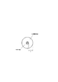
図1は、本実施形態における、電磁波導波路の概略構成図である。図1のように、本実施形態の電磁波導波路は、単一線101、誘電体部材102、入力又は出力或いはその両方を行うための電磁波結合部103(a)、103(b)で構成される。単一線101は、導体で構成される。
FIG. 1 is a schematic configuration diagram of an electromagnetic wave waveguide in the present embodiment. As shown in FIG. 1, the electromagnetic wave waveguide of the present embodiment includes a
図2は、本実施形態の電磁波導波路において電磁波が伝搬する部分の断面図である。図2のように、本実施形態の電磁波導波路は、単一線101に対して、誘電体部材102を被膜する構成である。図2中のdは、誘電体部材102の被膜厚みであり、単一線101と誘電体部材102の界面から誘電体部材102の外周面までの距離となる。図2では、被膜厚みdは、一様な厚みで表現されているが、必ずしも一様である必要はない。部分的に、厚みが変化する形態も可能である。つまり、図2では、単一線101と誘電体部材102の断面は、円形状であるが、この形状だけではなく、様々な形状を取り得る。
FIG. 2 is a cross-sectional view of a portion where an electromagnetic wave propagates in the electromagnetic wave waveguide of the present embodiment. As shown in FIG. 2, the electromagnetic wave waveguide of the present embodiment has a configuration in which the
図1のように、本実施形態の電磁波導波路は、電磁波結合部103(a)、103(b)を有している。電磁波結合部103(a)、103(b)は、外部又は内部で発生したテラヘルツ波を、電磁波が伝搬する導波路部分に結合させる働きを持つ。図1では、この電磁波結合部103(a)、103(b)は、導波路部分を構成する単一線101と誘電体部材102に対して、独立して描かれている。しかし、実際には、導波路部分と密着して構成され、誘電体部材102によって、内部支持(内包される)又は外部支持される。また、図1において、電磁波結合部は2つ描かれているが、これに限るものではない。導波路の構成によっては、1つであってもよいし、2つ以上あってもよい。また、電磁波結合部の位置は、図1の形態では、単一線101と誘電体部材102の端部にあるが、この位置も任意である。
As shown in FIG. 1, the electromagnetic wave waveguide of this embodiment has electromagnetic wave coupling portions 103 (a) and 103 (b). The electromagnetic wave coupling portions 103 (a) and 103 (b) have a function of coupling terahertz waves generated outside or inside to a waveguide portion where the electromagnetic waves propagate. In FIG. 1, the electromagnetic wave coupling portions 103 (a) and 103 (b) are drawn independently with respect to the
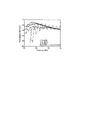
図3は、電磁波導波路のうち、単一線101と誘電体部材102によって構成される電磁波伝送部分の伝搬特性の計算結果を示す。ここで、単一線101として、直径10μm、長さ1mmの金を用いている。また、誘電体部材102として、BCB(ベンゾシクロブテン)を用いている。計算では、単一線101に対して誘電体部材102を同心円状に配置し、被膜厚みdを変化させている。ただし、単一線101と誘電体部材102の材料はこれに限るものではない。単一線101としては、導体であればよい。誘電体部材102としては、使用する電磁波に対して、損失、分散が小さい物が望ましい。また、長さに関しても制限はなく、ファイバ状の導波路としてもよい。
FIG. 3 shows the calculation result of the propagation characteristics of the electromagnetic wave transmission portion constituted by the
上記計算は有限積分法を用いて行った。ここでは、被膜厚みdを、50μm(図中■)、150μm(図中●)、250μm(図中▲)と変化させた時の伝搬特性に加え、誘電体部材102がない場合の計算結果(図中□)も比較のため掲載している。図3によると、単一線101に対して誘電体部材102で被膜した構成の方が、誘電体部材102がない構成よりも、伝搬特性が向上している様子がわかる。また、被膜厚みdは、厚いほど伝搬特性が向上する様子がわかる。単一線101のみの場合の電磁界分布を観測すると、電磁界は、同軸ケーブルと同じくTEMモードで伝搬することがわかった。誘電体部材102が存在する場合でも、この伝搬モードは変わらない。
The above calculation was performed using a finite integration method. Here, in addition to the propagation characteristics when the coating thickness d is changed to 50 μm (■ in the figure), 150 μm (● in the figure), and 250 μm (▲ in the figure), the calculation result when there is no dielectric member 102 ( □) in the figure is also included for comparison. According to FIG. 3, it can be seen that the configuration in which the
誘電体部材102の被膜厚みdが小さい場合、誘電体部材102の外周面において、電磁界が反射される傾向が観測された。これは、外周面の境界における屈折率差に起因する反射であり、誘電体部材102と外部との屈折率差が大きくなるほど、この傾向は強くなる。このような電磁界の反射の程度によっては、電磁界の伝搬モードを乱す要因になる。また、被膜厚みdが小さいと、誘電体部材102より外部へ漏れる電磁界成分が多くなる。検証の結果、電磁波導波路を伝搬する電磁波の実効波長λに対して被膜厚みを1/2λ以上確保することによって、殆どの電磁界成分を誘電体部材102内に閉じ込められることを確認した。使用する電磁波が、ある周波数帯域を有している場合、この実効波長は、電磁波の周波数帯域のうち、最低周波数の実効波長である。このような被膜厚さdの条件を用いることによって、本実施形態の電磁波導波路は、外部の影響を効果的に受け難くしつつ、低損失・低分散な特性を得ることができる。
When the coating thickness d of the
尚、図3の計算では、電磁波導波路を同心円状としているが、誘電体部材102の形状が変化しても、同様の結果が得られることを確認している。電磁波導波路の設計において重要なのは、単一線101と誘電体部材102とが接する界面から、誘電体部材102の外周面までの最短距離が、1/2λ以上確保されていることである。そのため、この条件が成立している限り、誘電体部材102の形状は任意である。
In the calculation of FIG. 3, the electromagnetic wave waveguide is concentric, but it has been confirmed that the same result can be obtained even if the shape of the
また、図3では、低周波側の伝搬特性に対して、高周波側の伝搬特性があまり向上していないが、これは、誘電体部材102に使用する誘電体材料の物性(誘電率など)の周波数依存特性に起因するものである。例えば、誘電体部材102として、高抵抗シリコン(これはテラヘルツ波に対する透明度が高い)などの物質を使用した場合、高周波側の伝搬特性も改善することがわかっている。上述した如く被膜厚みを1/2λ以上確保することは好適であるが、勿論、誘電体部材の被膜厚みを1/2λ以下にした場合であっても、一定程度、外部の影響を受け難くできて、比較的低損失・低分散な特性を持つ電磁波導波路を得ることができる。
Further, in FIG. 3, the propagation characteristics on the high frequency side are not so much improved as compared with the propagation characteristics on the low frequency side, but this is due to the physical properties (dielectric constant, etc.) of the dielectric material used for the
以上のように、本実施形態の構成により、誘電体部材内部に、電磁界を集中させ、大気に漏れるテラヘルツ波を抑制することにより、大気による減衰を抑え、高効率な電磁波の伝送を実現できる。また、テラヘルツ波の電磁界は、誘電体部材内部に集中している。そのため、電磁波導波路外部の雰囲気が変化(例えば、湿度が変化する)する場合や、電磁波導波路近傍に、電磁界を乱すような素子(例えば、金属を含む素子)が存在する場合であっても、テラヘルツ波の電磁界分布には、殆ど影響がない。こうして、安定な伝送特性を得ることができる。 As described above, with the configuration of the present embodiment, the electromagnetic field is concentrated inside the dielectric member, and the terahertz wave leaking to the atmosphere is suppressed, so that attenuation by the atmosphere can be suppressed and highly efficient transmission of electromagnetic waves can be realized. . Further, the electromagnetic field of the terahertz wave is concentrated inside the dielectric member. Therefore, when the atmosphere outside the electromagnetic wave waveguide changes (for example, the humidity changes), or when an element (for example, an element containing metal) that disturbs the electromagnetic field exists in the vicinity of the electromagnetic wave waveguide. However, there is almost no influence on the electromagnetic field distribution of the terahertz wave. In this way, stable transmission characteristics can be obtained.
つまり、本実施形態の電磁波導波路は、外部の影響を受け難いという効果がある。よって、電磁波導波路の取り扱いも簡易になる。また、誘電体部材内に、テラヘルツ波の電磁界が集中するということは、本実施形態の電磁波導波路を近接させても、それぞれの導波路に影響を及ぼすことがないので、テラヘルツ波を用いた装置の集積化、小型化が容易になる。 That is, the electromagnetic wave waveguide of this embodiment has an effect that it is not easily affected by the outside. Therefore, handling of the electromagnetic wave waveguide is also simplified. Further, the concentration of the terahertz wave electromagnetic field in the dielectric member means that even if the electromagnetic wave waveguides of this embodiment are brought close to each other, the respective waveguides are not affected. This makes it easier to integrate and downsize the existing equipment.
また、本実施形態の電磁波導波路は、誘電体部材によって、電磁波結合部分を内包、又は外部支持する構成である。そのため、従来必要であった、電磁波結合部分を空間配置するための部材が不要になり、導波路構成が簡易になる。また、これを装置に応用した場合、装置構成の小型化が容易になる。また、電磁波結合部分は誘電体部材によって支持される構成であるので、単一線と電磁波結合部分の位置関係は常に一定である。そのため、外部から飛来するテラヘルツ波との結合条件が常に一定であり、従来必要であった、結合状態の調整作業が不要になって、扱いが簡易になる。さらに、このような調整作業が不要になるので、常に安定した結合状態を実現でき、信頼性の高い電磁波導波路を提供できる。 In addition, the electromagnetic wave waveguide of the present embodiment is configured to include or externally support the electromagnetic wave coupling portion with a dielectric member. This eliminates the need for a member for spatially arranging the electromagnetic wave coupling portion, which has been conventionally required, and simplifies the waveguide configuration. In addition, when this is applied to an apparatus, it is easy to reduce the size of the apparatus configuration. Further, since the electromagnetic wave coupling portion is supported by the dielectric member, the positional relationship between the single line and the electromagnetic wave coupling portion is always constant. For this reason, the coupling condition with the terahertz wave flying from the outside is always constant, and the adjustment of the coupling state, which has been conventionally required, becomes unnecessary, and the handling becomes simple. Furthermore, since such adjustment work becomes unnecessary, a stable coupling state can be realized at all times, and a highly reliable electromagnetic wave waveguide can be provided.
これらの点について、非特許文献1の技術では、図10のように、単一線1001にテラヘルツ波1003を結合させるために、さらに単一線1002を用いている。単一線1002は、単一線1001の長手方向に対して単一線1002の長手方向が垂直に交差するように空間配置し、空間を伝搬するテラヘルツ波1003を単一線間に結合させるものである。
Regarding these points, in the technique of
したがって、例えば、外部の影響を排除するため、単一線1001を空間に孤立配置させるような場合、テラヘルツ波の結合に用いる単一線1002も空間に配置する必要がある。このように、各単一線を、空間配置させるための部材が別途必要になるため、結果的に導波路の構成が大きくなる。さらに、導波路自体の空間配置や、各単一線の空間配置を行うための調整作業も必要である。特に、単一線1001へのテラヘルツ波の結合状態は、各単一線の空間配置によって影響を受けることが予想される。そのため、このような各単一線を空間配置する方法では、同じテラヘルツ波の結合状態を再現するために、精密な空間位置決めが必要であり、調整作業が難しい。 Therefore, for example, when the single line 1001 is isolated in the space in order to eliminate external influences, the single line 1002 used for coupling the terahertz waves needs to be also arranged in the space. Thus, since a member for spatially arranging each single line is required, the structure of the waveguide increases as a result. Furthermore, adjustment work for spatial arrangement of the waveguide itself and spatial arrangement of each single line is also necessary. In particular, the terahertz wave coupling state to the single line 1001 is expected to be affected by the spatial arrangement of each single line. Therefore, in such a method of spatially arranging each single line, in order to reproduce the same coupled state of terahertz waves, precise spatial positioning is necessary, and adjustment work is difficult.
以下に、より具体的な実施例について、図面を参照して説明する。 Hereinafter, more specific embodiments will be described with reference to the drawings.
(実施例1)
実施例1は、電磁波結合部103としてグレーティング構造401を用いて、空間を伝搬するテラヘルツ波を、単一線101と誘電体部材102で構成される導波路に結合する構成例である。
(Example 1)
The first embodiment is a configuration example in which a terahertz wave propagating in space is coupled to a waveguide composed of a
実施例1では、図4に示すように、電磁波結合部103であるグレーティング構造401は、矩形断面の単一線101の任意の位置に刻まれている。このような単一線101を、液状の誘電体部材102で満たされた型に挿入し、熱によって誘電体部材102を硬化させることによって本実施例の電磁波導波路を作製することができる。勿論、作製方法はこれに限るものではなく、既知のプロセス技術を用いることができる。電磁波結合部103として、グレーティング構造401を用いた場合、本実施例の電磁波導波路は、空間を伝搬するテラヘルツ波のうち、グレーティングの周期に応じた波長のテラヘルツ波を、選択的に伝搬させることができる。
In the first embodiment, as shown in FIG. 4, the grating structure 401 that is the electromagnetic
(実施例2)
図5は実施例2を示す。図5では、空間を伝搬するテラヘルツ波を導波路に結合する電磁波結合部103として、クロスワイヤ構造501を用いている。クロスワイヤ構造501は、単一線101に対して、導体がほぼ垂直に配置される構造である。作製方法としては、例えば、単一線101を内包する誘電体部材102の外周面上に、クロスワイヤ構造501をパターニングするという手法がある。ただし、作製方法はこれに限るものではない。また、図5のクロスワイヤ構造501は、誘電体部材102の外周面上に作製されているが、誘電体部材102の内部に埋め込まれていてもよい。電磁波結合部103として、クロスワイヤ構造501を用いた場合、非特許文献1にみられるように、空間を伝搬するテラヘルツ波に対して、広帯域な周波数領域を有するテラヘルツ波を伝搬させることができる。
(Example 2)
FIG. 5 shows Example 2. In FIG. 5, a cross-wire structure 501 is used as an electromagnetic
電磁波結合部103の構成としては、上記実施例1、2のものに限るものではない。例えば、アンテナ構造なども使用可能である。要は、空間を伝搬するテラヘルツ波を、導波路に結合できる構成であればよい。尚、電磁波結合部103として、空間を伝搬するテラヘルツ波を導波路に伝搬させる入力部分の構成を説明したが、これらの構成は、そのまま出力部分にも適用できる。
The configuration of the electromagnetic
実施例1、2のような構造を有することによって、単一線101と誘電体部材102で構成される導波路へテラヘルツ波が結合する結合条件を一定にできるため、結合のための調整作業を簡略化することができる。
By having the structure as in the first and second embodiments, the coupling condition for coupling the terahertz wave to the waveguide composed of the
(実施例3)
実施例3は、電磁波結合部103がテラヘルツ波を発生する機能を有し、単一線101と誘電体部材102で構成される導波路にテラヘルツ波を結合する構成例である。
(Example 3)
The third embodiment is a configuration example in which the electromagnetic
実施例3では、図6に示すように、電磁波結合部103として、光伝導スイッチ構造601を用いている。図6のように、光伝導スイッチ構造601は、ある微小間隔で隔たった、単一線101から引き出された電極602と誘電体部材102の一部に形成された電極603を備える。そして、これらに対して、その間隙に、キャリヤ移動度が高くキャリヤのライフタイムが短い半導体(例えば、低温成長ガリウムヒ素:LT-GaAs)を密着させている。光伝導スイッチ構造601の動作は、上記した間隙部分に電界を印加した状態で、超短パルスレーザ光を用いて外部より光学的にゲートすることで、テラヘルツ波を発生させる。そして、光伝導スイッチ構造601で発生したテラヘルツ波は、単一線101と誘電体部材102で構成される導波路に結合し伝搬する。これらの電極602、603は、既知のプロセスによってパターニングされる。また、光伝導スイッチ構造601を構成する半導体は、例えば、薄膜化し、誘電体部材102に貼付けられる。
In the third embodiment, as shown in FIG. 6, a photoconductive switch structure 601 is used as the electromagnetic
尚、本実施例において、光伝導スイッチ構造601は、単一線101と誘電体部材102で構成される導波路の端面に形成されているが、この構成に限るものではない。誘電体部材102の内部又は外周面上に形成されてもよい。また、電極603は、単一線101に対して、同心円状にパターニングされている。この理由は、単一線101と誘電体部材102で構成される導波路の伝搬モードが同軸ケーブルと同じTEMモードであることに着目し、より結合状態を良好に保つために、テラヘルツ波発生側の構造も同軸構造とするためである。しかし、重要なのは、光伝導スイッチ構造601を構成する導体の間隙に電界が印加されればよいので、当然、この同軸構造に限るものではない。
In the present embodiment, the photoconductive switch structure 601 is formed on the end face of the waveguide constituted by the
(実施例4)
実施例4は、電磁波結合部103がテラヘルツ波を発生する機能を有し、単一線101と誘電体部材102で構成される導波路にテラヘルツ波を結合する別の構成例である。本実施例では、図7に示すように、電磁波結合部103として、電磁波利得構造701を用いている。図7のように、電磁波利得構造701は、ある微小間隔で隔たった、単一線101から引き出された電極702と誘電体部材102の一部に形成された電極703に対して、テラヘルツ波領域に利得がある電磁波利得物質を密着させた構造である。
(Example 4)
The fourth embodiment is another configuration example in which the electromagnetic
電磁波利得物質は、例えば、共鳴トンネルダイオード(RTD)やガンダイオードなどに代表される電磁波利得を得られる半導体素子である。上述したように、この電磁波利得物質は、テラヘルツ波のうち、所望の周波数帯で利得を得るように設計されている。そのため、電磁波利得構造701の両端の電極702、703に電界を印加することで、テラヘルツ波を発生することができる。そして、電磁波利得構造701で発生したテラヘルツ波は、単一線101と誘電体部材102で構成される導波路に結合し伝搬する。これらの電極702、703も、既知のプロセスによってパターニングされる。
The electromagnetic wave gain material is a semiconductor element that can obtain an electromagnetic wave gain represented by, for example, a resonant tunnel diode (RTD), a Gunn diode, or the like. As described above, this electromagnetic wave gain material is designed to obtain gain in a desired frequency band of terahertz waves. Therefore, terahertz waves can be generated by applying an electric field to the
尚、本実施例においても、電磁波利得構造701は、単一線101と誘電体部材102で構成される導波路の端面に形成されているが、この構成に限るものではない。誘電体部材601の内部又は外周面上に形成されてもよい。また、電極703も、単一線101に対して、同心円状にパターニングされている。この理由は、上記実施例3のところで説明した通りである。ここでも、電磁波利得構造701を構成する導体の間隙に電界が印加されればよいので、この同軸構造に限らない。
In this embodiment as well, the electromagnetic wave gain structure 701 is formed on the end face of the waveguide constituted by the
実施例3、4では、電磁波結合部103として、テラヘルツ波を発生させる部分の構成を示しているが、これらの構成は、そのまま検出部分にも適応させられることは言うまでもない。
In the third and fourth embodiments, the configuration of the portion that generates the terahertz wave is shown as the electromagnetic
上記実施例3、4のような構成を有することにより、電磁波結合部103で発生したテラヘルツ波は、単一線101と誘電体部材102で構成される導波路を伝搬する。ここでは、電磁波結合部103が、テラヘルツ波を発生及び検出するような構成を有しているので、装置構成が小型になるという効果がある。
By having the configuration as in the third and fourth embodiments, the terahertz wave generated in the electromagnetic
(実施例5)
実施例5は、電磁波結合部103が導波路変換機能を有し、他の高周波モジュールを伝搬するテラヘルツ波を、単一線101と誘電体部材102で構成される導波路に結合する構成例である。
(Example 5)
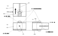
Example 5 is a configuration example in which the electromagnetic
本実施例では、図8に示すように、電磁波結合部103として、導波路変換構造801を用いている。図8は、上面図(a)、断面図(b)、側面図(c)を示したものである。図8のように、導波路変換構造801は、誘電体部材102と第1導体802と第2導体803で構成される伝送線路(マイクロストリップ線路)に対し、第1導体802と第2導体803の間に、単一線101の端部が挿入される構造である。このような構造を有することにより、高周波モジュール内を伝搬するテラヘルツ波は、導波路変換構造801において、単一線101と誘電体部材102で構成される導波路に結合し、伝搬する。
In this embodiment, as shown in FIG. 8, a waveguide conversion structure 801 is used as the electromagnetic
尚、導波路変換構造801を構成する伝送線路構造は、図8に示したようなマイクロストリップ線路に限るものではない。例えば、コプレーナ導波路など、高周波電磁波信号を伝搬するために用いるような伝送線路構造も利用できる。また、導波管や同軸構造など、立体的な導波路構造も適用できる。また、導波路変換構造801において、インピーダンスの不整合を軽減し、テラヘルツ波の結合状態をさらに良好にするため、単一線101や誘電体部材102の形状が部分的に変化する態様も考えられる。例えば、導波路変換構造801の端部において、単一線101や誘電体部材102のサイズを部分的に太くすることや、細くすること、又はテーパ形状を用いることなどが考えられる。
The transmission line structure constituting the waveguide conversion structure 801 is not limited to the microstrip line as shown in FIG. For example, a transmission line structure used for propagating a high-frequency electromagnetic wave signal such as a coplanar waveguide can also be used. A three-dimensional waveguide structure such as a waveguide or a coaxial structure can also be applied. Further, in the waveguide conversion structure 801, in order to reduce impedance mismatching and further improve the terahertz wave coupling state, a mode in which the shapes of the
ここでは、電磁波結合部103として、他の高周波モジュールを伝搬するテラヘルツ波を、本実施例の電磁波導波路に適応するように変換し結合させる構成を示した。しかし、これらの構成は、そのまま、本実施例の電磁波導波路を伝搬するテラヘルツ波を、他の高周波モジュールに結合させる構成にも適用できることは言うまでもない。
Here, as the electromagnetic
以上のような構成を有することにより、他の高周波モジュールを伝搬するテラヘルツ波を、本実施例の電磁波導波路構造に結合させ、伝搬させることができる。例えば、テラヘルツ波の信号制御などを行う機能的な部分を、これまでの一般的な伝送線路を用いた高周波回路で行い、伝送部分のみを本実施例の電磁波導波路で行うことなどをすることができる。これにより、伝送線路で問題となっていた信号の減衰や分散を抑制できる。そのため、より複雑で機能性に富んだ高周波モジュールを容易に提供することができる。 With the above configuration, terahertz waves propagating through other high-frequency modules can be coupled and propagated to the electromagnetic wave waveguide structure of the present embodiment. For example, a functional part that performs terahertz wave signal control or the like is performed by a conventional high-frequency circuit using a transmission line, and only the transmission part is performed by the electromagnetic wave waveguide of this embodiment. Can do. As a result, it is possible to suppress the attenuation and dispersion of the signal that has been a problem in the transmission line. Therefore, it is possible to easily provide a high-frequency module that is more complicated and rich in functionality.
4 物体
101 単一線
102 誘電体部材
103 電磁波結合部
401 グレーティング構造
501 クロスワイヤ構造
601 光伝導スイッチ構造
602 電極
603 電極
701 電磁波利得構造
702 電極
703 電極
801 導波路変換構造
802 第1導体
803 第2導体
1001 単一線
1002 単一線
1003 テラヘルツ波
4 objects
101 single line
102 Dielectric material
103 Electromagnetic coupling
401 grating structure
501 Cross wire structure
601 photoconductive switch structure
602 electrode
603 electrodes
701 Electromagnetic gain structure
702 electrode
703 electrode
801 Waveguide conversion structure
802 1st conductor
803 Second conductor
1001 single line
1002 single line
1003 terahertz wave
Claims (6)
導電体で形成される単一線と、前記単一線を覆う誘電体部材とを備えることを特徴とする電磁波導波路。 An electromagnetic wave waveguide for transmitting an electromagnetic wave having an arbitrary frequency region of 30 GHz to 30 THz,
An electromagnetic wave waveguide comprising: a single line formed of a conductor; and a dielectric member that covers the single line.
Priority Applications (1)
| Application Number | Priority Date | Filing Date | Title |
|---|---|---|---|
| JP2005255777A JP2007074043A (en) | 2005-09-05 | 2005-09-05 | Electromagnetic wave waveguide |
Applications Claiming Priority (1)
| Application Number | Priority Date | Filing Date | Title |
|---|---|---|---|
| JP2005255777A JP2007074043A (en) | 2005-09-05 | 2005-09-05 | Electromagnetic wave waveguide |
Publications (2)
| Publication Number | Publication Date |
|---|---|
| JP2007074043A true JP2007074043A (en) | 2007-03-22 |
| JP2007074043A5 JP2007074043A5 (en) | 2008-09-04 |
Family
ID=37935159
Family Applications (1)
| Application Number | Title | Priority Date | Filing Date |
|---|---|---|---|
| JP2005255777A Pending JP2007074043A (en) | 2005-09-05 | 2005-09-05 | Electromagnetic wave waveguide |
Country Status (1)
| Country | Link |
|---|---|
| JP (1) | JP2007074043A (en) |
Cited By (2)
| Publication number | Priority date | Publication date | Assignee | Title |
|---|---|---|---|---|
| JP2017506018A (en) * | 2013-12-10 | 2017-02-23 | エイ・ティ・アンド・ティ インテレクチュアル プロパティ アイ,エル.ピー. | Quasi-optical coupler |
| US11469337B2 (en) | 2019-09-24 | 2022-10-11 | Samsung Electronics Co., Ltd. | Optically controlled millimeter-wave switch based on substrate integrated waveguide |
Citations (4)
| Publication number | Priority date | Publication date | Assignee | Title |
|---|---|---|---|---|
| US3134951A (en) * | 1961-09-28 | 1964-05-26 | Rohde & Schwarz | Coupling between stationary launching means and movable surface wave guide means |
| US4489601A (en) * | 1983-07-18 | 1984-12-25 | Sperry Corporation | Apparatus and method of measuring the level of a liquid |
| JPH11261331A (en) * | 1998-03-10 | 1999-09-24 | Hitachi Ltd | Interrogator antenna for non-contact ic card system |
| US6384700B1 (en) * | 1989-07-13 | 2002-05-07 | Itt Manufacturing Enterprises, Inc. | Towed antenna system right angle feed for towed antenna system rapid deployment cable and towed antenna system |
-
2005
- 2005-09-05 JP JP2005255777A patent/JP2007074043A/en active Pending
Patent Citations (4)
| Publication number | Priority date | Publication date | Assignee | Title |
|---|---|---|---|---|
| US3134951A (en) * | 1961-09-28 | 1964-05-26 | Rohde & Schwarz | Coupling between stationary launching means and movable surface wave guide means |
| US4489601A (en) * | 1983-07-18 | 1984-12-25 | Sperry Corporation | Apparatus and method of measuring the level of a liquid |
| US6384700B1 (en) * | 1989-07-13 | 2002-05-07 | Itt Manufacturing Enterprises, Inc. | Towed antenna system right angle feed for towed antenna system rapid deployment cable and towed antenna system |
| JPH11261331A (en) * | 1998-03-10 | 1999-09-24 | Hitachi Ltd | Interrogator antenna for non-contact ic card system |
Cited By (2)
| Publication number | Priority date | Publication date | Assignee | Title |
|---|---|---|---|---|
| JP2017506018A (en) * | 2013-12-10 | 2017-02-23 | エイ・ティ・アンド・ティ インテレクチュアル プロパティ アイ,エル.ピー. | Quasi-optical coupler |
| US11469337B2 (en) | 2019-09-24 | 2022-10-11 | Samsung Electronics Co., Ltd. | Optically controlled millimeter-wave switch based on substrate integrated waveguide |
Similar Documents
| Publication | Publication Date | Title |
|---|---|---|
| JP4878180B2 (en) | Inspection equipment using electromagnetic waves | |
| JP4732201B2 (en) | Sensing device using electromagnetic waves | |
| Cong et al. | Spatiotemporal dielectric metasurfaces for unidirectional propagation and reconfigurable steering of terahertz beams | |
| Balram et al. | Coherent coupling between radiofrequency, optical and acoustic waves in piezo-optomechanical circuits | |
| JP4955966B2 (en) | Waveguide, device using the same, and detection method | |
| JP4646838B2 (en) | Probe and near-field microscope | |
| JP4975000B2 (en) | Electromagnetic wave generating element, electromagnetic wave integrated element, and electromagnetic wave detecting device | |
| JP5419411B2 (en) | Terahertz wave generator | |
| US7409132B2 (en) | Plastic waveguide for terahertz wave | |
| Navarro-Cía et al. | Silver-coated Teflon tubes for waveguiding at 1–2 THz | |
| Liu et al. | Integration of Brillouin and passive circuits for enhanced radio-frequency photonic filtering | |
| JP6075822B2 (en) | Sensor device | |
| JPH02181634A (en) | Scan chip | |
| US9244331B2 (en) | Electromagnetic wave generating device, electromagnetic wave detecting device, and time-domain spectroscopy apparatus | |
| Kaur et al. | Affordable terahertz components using 3D printing | |
| Pan et al. | Guided reflectometry imaging unit using millimeter wave FMCW radars | |
| JP4636917B2 (en) | Sample holding device, sample detection apparatus and sample detection method using the same | |
| JP2007074043A (en) | Electromagnetic wave waveguide | |
| JP6367753B2 (en) | Dielectric spectroscopy sensor | |
| Kang et al. | Frequency comb measurements for 6G terahertz nano/microphotonics and metamaterials | |
| WO2022025141A1 (en) | Dielectric waveguide, terahertz circuit, and terahertz integrated circuit | |
| QIU et al. | Efficient free-space-to-chip coupling of ultra-wideband sub-ps THz pulse for biomolecule fingerprint sensing |
Legal Events
| Date | Code | Title | Description |
|---|---|---|---|
| A521 | Written amendment |
Free format text: JAPANESE INTERMEDIATE CODE: A523 Effective date: 20080718 |
|
| A621 | Written request for application examination |
Free format text: JAPANESE INTERMEDIATE CODE: A621 Effective date: 20080718 |
|
| A977 | Report on retrieval |
Free format text: JAPANESE INTERMEDIATE CODE: A971007 Effective date: 20100127 |
|
| A131 | Notification of reasons for refusal |
Free format text: JAPANESE INTERMEDIATE CODE: A131 Effective date: 20100204 |
|
| A521 | Written amendment |
Free format text: JAPANESE INTERMEDIATE CODE: A523 Effective date: 20100330 |
|
| A131 | Notification of reasons for refusal |
Free format text: JAPANESE INTERMEDIATE CODE: A131 Effective date: 20110119 |
|
| A02 | Decision of refusal |
Free format text: JAPANESE INTERMEDIATE CODE: A02 Effective date: 20110906 |