KR100794889B1 - Liquid crystal alignment - Google Patents
Liquid crystal alignment Download PDFInfo
- Publication number
- KR100794889B1 KR100794889B1 KR1020010015982A KR20010015982A KR100794889B1 KR 100794889 B1 KR100794889 B1 KR 100794889B1 KR 1020010015982 A KR1020010015982 A KR 1020010015982A KR 20010015982 A KR20010015982 A KR 20010015982A KR 100794889 B1 KR100794889 B1 KR 100794889B1
- Authority
- KR
- South Korea
- Prior art keywords
- orientation
- liquid crystal
- shapes
- cell wall
- posts
- Prior art date
Links
Images


Classifications
-
- G—PHYSICS
- G02—OPTICS
- G02F—OPTICAL DEVICES OR ARRANGEMENTS FOR THE CONTROL OF LIGHT BY MODIFICATION OF THE OPTICAL PROPERTIES OF THE MEDIA OF THE ELEMENTS INVOLVED THEREIN; NON-LINEAR OPTICS; FREQUENCY-CHANGING OF LIGHT; OPTICAL LOGIC ELEMENTS; OPTICAL ANALOGUE/DIGITAL CONVERTERS
- G02F1/00—Devices or arrangements for the control of the intensity, colour, phase, polarisation or direction of light arriving from an independent light source, e.g. switching, gating or modulating; Non-linear optics
- G02F1/01—Devices or arrangements for the control of the intensity, colour, phase, polarisation or direction of light arriving from an independent light source, e.g. switching, gating or modulating; Non-linear optics for the control of the intensity, phase, polarisation or colour
- G02F1/13—Devices or arrangements for the control of the intensity, colour, phase, polarisation or direction of light arriving from an independent light source, e.g. switching, gating or modulating; Non-linear optics for the control of the intensity, phase, polarisation or colour based on liquid crystals, e.g. single liquid crystal display cells
- G02F1/133—Constructional arrangements; Operation of liquid crystal cells; Circuit arrangements
- G02F1/1333—Constructional arrangements; Manufacturing methods
- G02F1/1337—Surface-induced orientation of the liquid crystal molecules, e.g. by alignment layers
- G02F1/13378—Surface-induced orientation of the liquid crystal molecules, e.g. by alignment layers by treatment of the surface, e.g. embossing, rubbing or light irradiation
Abstract
액정 장치는 소정의 배향을 만들기 위한 형태 및/또는 방위를 갖는 배향 형상들(10)의 어레이를 포함한 표면 배향 구조를 갖는다. 형상들의 기하학적 구조와 간격에 따라, 액정은 평면, 틸트, 또는 수직 배향을 채택하도록 유도될 수 있다. The liquid crystal device has a surface alignment structure that includes an array of alignment shapes 10 having a shape and / or orientation to make a desired alignment. Depending on the geometry and spacing of the shapes, the liquid crystal can be induced to adopt a planar, tilt, or vertical orientation.
액정 장치, 배향 형상들, 표면 배향 구조, 평면, 틸트, 수직Liquid Crystal Device, Orientation Shapes, Surface Orientation Structure, Plane, Tilt, Vertical
Description
도 1은 본 발명에 따른 하나의 포스트 및 그 주위의 LC의 개략적인 단면도이다. 이 단면은 x, y 평면에 있다. 타원들은 로컬 방향자에 대응한 장축을 갖는 LC 분자들을 나타낸다. 1 is a schematic cross-sectional view of one post and its LC in accordance with the present invention. This cross section is in the x, y plane. Ellipses represent LC molecules with a long axis corresponding to the local director.
도 2는 본 발명의 일 특징에 따른 쌍안정 네마틱 장치의 하나의 포스트 및 그 주위의 LC의 개략적인 단면도들로서 서로 다른 상태에서 포스트의 사선들중의 하나를 따라 얼라인되는 것을 도시한다. Figure 2 is a schematic cross sectional view of one post of a bistable nematic device and its surrounding LC in accordance with an aspect of the present invention, showing alignment along one of the diagonals of the post in different states.
도 3은 본 발명의 일 특징에 따른 쌍안정 네마틱 장치의 하나의 포스트 및 그 주위의 LC의 개략적인 단면도들로서 서로 다른 상태에서 포스트의 사선들중의 하나를 따라 얼라인되는 것을 도시한다.Figure 3 is a schematic cross sectional view of one post of a bistable nematic device and its surrounding LC in accordance with an aspect of the present invention, showing alignment along one of the diagonals of the post in different states.
도 4는 본 발명에 따른 장치의 단위 셀 평면도로서 의사랜덤(pseudorandom) 어레이로 배열된 포스트들을 도시한다.4 shows posts arranged in a pseudorandom array as a unit cell plan view of the apparatus according to the invention.
도 5 및 도 6은 본 발명의 일 특징에 따라, 두 상태들 간의 스위칭에 대해 실험 셀의 투과도가 펄스 길이 및 진폭의 함수로 변화하는 것을 도시한다. 5 and 6 show that the transmittance of the experimental cell changes as a function of pulse length and amplitude for switching between two states, in accordance with an aspect of the present invention.
도 7 내지 도 10은 본 발명에 따른 액정 장치의 제조에 사용된 포스트들의 어레이의 SEM 현미경 사진들을 나타낸다.7 to 10 show SEM micrographs of an array of posts used in the manufacture of a liquid crystal device according to the invention.
도 11은 본 발명의 다른 특징에 따른 장치의, 셀 벽들에 수직하고, 포스트의 측면에 평행하고 근접한 단면도이다.11 is a cross-sectional view perpendicular to the cell walls, parallel to and close to the side of the post, of an apparatus according to another feature of the invention.
도 12는 삼각 포스트에 대한, 도 1과 유사한 개략적인 단면도이다.12 is a schematic cross-sectional view similar to FIG. 1 for a triangular post.
도 13은 타원 포스트에 대한, 도 1과 유사한 개략적인 단면도이다.FIG. 13 is a schematic cross-sectional view similar to FIG. 1 for an elliptical post. FIG.
도 14 내지 20은 본 발명의 다른 실시예들에 따른 장치들의 형상들의 상이한 어레이들을 도시한 도면들이다. 14-20 illustrate different arrays of shapes of devices in accordance with other embodiments of the present invention.
<도면의 주요 부분에 대한 부호의 설명><Explanation of symbols for the main parts of the drawings>
2: 제1 셀 벽2: first cell wall
4: 제2 셀 벽4: second cell wall
6: 애널라이저6: analyzer
8: 편광자8: polarizer
10: 사각 포스트10: square post
12: 행 전극12: row electrode
14: 열 전극14: column electrode
본 발명은 액정 장치 내의 액정의 배향에 관한 것이다. The present invention relates to the orientation of liquid crystals in liquid crystal devices.
액정(Liquid Crystal, LC) 재료는 그의 장축과 단축을 따라 상이한 광학 특성을 갖는 막대형(lod-like) 또는 욋가지형(lath-like) 분자들이다. 분자들은 어느 정도 긴 범위의 서열을 가져서 지엽적으로 그들은 그들 가까이에 있는 이웃하는 분자들과 유사한 방향을 가지려는 경향이 있다. 분자들의 장축의 로컬 방위는 "방향자(director)"라고 일컬어진다. 세가지 타입의 LC 재료, 즉 네마틱(nematic), 콜레스테릭(cholesteric, 카이럴 네마틱; chiral nematic) 및 스멕틱(smectic)이 있다. 디스플레이 장치에 사용되는 액정에 대해서는, "오프" 상태로 정의되는 방식과 "온" 상태로 정의되는 다른 방식으로 얼라인되도록 만들어져서, 디스플레이가 각 상태에서 상이한 광학 특성을 갖는다. 두가지 주요 배향들로는 수직(homeotropic, 이 방식에서 방향자는 셀 벽들의 평면에 대해 거의 수직임)과 평면(planar, 이 방식에서 방향자는 셀 벽들의 평면에 대해 거의 평행하게 기울어짐)가 있다. 실제로, 평면 배향은 셀 벽의 평면에 대해 틸트되어 질 수 있고, 이러한 틸트는 스위칭을 보조하는 데에 유용할 수 있다. 본 발명은 액정 디스플레이에서의 배향에 관련된다.Liquid crystal (LC) materials are rod-like or lath-like molecules with different optical properties along their major and minor axes. Molecules have a long range of sequences, and locally they tend to have a similar orientation to neighboring molecules near them. The local orientation of the long axis of the molecules is called the "director". There are three types of LC materials: nematic, cholesteric, chiral nematic and smectic. For liquid crystals used in display devices, the display is made to be aligned in a manner defined by the "off" state and in another manner defined by the "on" state, so that the display has different optical properties in each state. The two main orientations are homeotropic (in this way the director is almost perpendicular to the plane of the cell walls) and planar (in this way the director is inclined almost parallel to the plane of the cell walls). In practice, the planar orientation can be tilted with respect to the plane of the cell wall, and this tilt can be useful to assist in switching. The present invention relates to orientation in liquid crystal displays.
하이브리드 얼라인드 네마틱(Hybrid Aligned Nematic, 이하, 'HAN'이라 함), 버티컬 얼라인드 네마틱(Vertical Aligned Nematic, 이하, 'VAN'이라 함), 트위스티드 네마틱(Twisted Nematic, 이하, 'TN'이라 함), 수퍼-트위스티드 네마틱(Super-Twisted Nematic, 이하, 'STN'이라 함) 셀들이 소비자에 의해 디스플레이 장치들 및 다른 제품들로서 광범위하게 사용된다. 셀들은 한쌍의 서로 대향하는, 그리고 그 사이에 네마틱 액정 재료를 개재한 채 서로 이격되어 있는 셀 벽들을 포함한다. 벽들은 투명한 전극 패턴들을 갖는데, 이 전극 패턴들은 그들 사이의 픽셀들을 정의한다. Hybrid Aligned Nematic (hereinafter referred to as HAN), Vertical Aligned Nematic (hereinafter referred to as "VAN"), Twisted Nematic (hereinafter referred to as "TN") Super-Twisted Nematic (hereinafter referred to as 'STN') cells are widely used by consumers as display devices and other products. The cells comprise a pair of cell walls facing each other and spaced apart from each other via a nematic liquid crystal material therebetween. The walls have transparent electrode patterns, which define the pixels between them.
TN과 STN 디스플레이에 있어서, 각각의 벽의 안쪽 표면은 네마틱 방향자의 평면 단방위 배향을 생성하되, 배향 방향이 서로 90도가 되도록 처리된다. 이러한 배열은 네마틱 방향자가 TN 셀 내의 1/4 헬릭스(helix)를 그리도록 야기하여, 픽셀이 "필드 오프" 상태일 때 편광이 90도만큼을 통해 가이드된다. STN 셀에서, 네마틱 액정은 카이럴 첨가제가 도핑되어, "필드 오프" 상태에서 편광면을 회전시키는 더 짧은 피치의 헬릭스를 생성한다. "필드 오프" 상태는, 셀이 편광자들과 교차하여 또는 평행하게 통해 관측되는 지에 따라 화이트이거나 블랙일 수 있다. 픽셀을 통해 전압을 인가하게 되면, 네마틱 방향자가 수직 방향으로 벽들에 수직으로 얼라인되도록 야기하여, 편광면이 "필드 온" 상태에서는 회전되지 않도록 한다. In TN and STN displays, the inner surface of each wall is processed to produce a planar unidirectional orientation of the nematic director, with the orientation directions 90 degrees to each other. This arrangement causes the nematic director to draw a quarter helix in the TN cell, so that the polarization is guided through 90 degrees when the pixel is in the "field off" state. In an STN cell, the nematic liquid crystal is doped with chiral additives to produce a shorter pitch helix that rotates the polarization plane in the "field off" state. The "field off" state may be white or black depending on whether the cell is observed through or parallel to the polarizers. Applying a voltage through the pixel causes the nematic director to align perpendicular to the walls in the vertical direction, such that the polarization plane is not rotated in the "field on" state.
HAN 셀에서, 한쪽 벽은 네마틱 LC를 수직 배향로 얼라인하도록 처리되고 다른 한쪽 벽은 평면 배향을 유도하도록 처리되는데, 통상 약간의 틸트를 사용하여 스위칭을 용이하게 한다. LC는 양의 유전율 비등방성을 가지며, 전계의 인가는 LC 방향자들이 벽들에 수직으로 얼라인하도록 야기하여, 셀이 복굴절성 "필드 오프" 상태로부터 비복굴절성 "필드 온" 상태로 전환한다.In a HAN cell, one wall is treated to align the nematic LC in a vertical orientation and the other wall is treated to induce a planar orientation, typically using a slight tilt to facilitate switching. LC has a positive dielectric anisotropy, and the application of an electric field causes the LC directors to align perpendicular to the walls, causing the cell to transition from a birefringent "field off" state to a non-birefringent "field on" state.
VAN 모드에서, 음의 유전율 비등방성을 가진 네마틱 LC가 "필드 오프" 상태에서 수직형으로 얼라인되고, "필드 온" 상태에서 복굴절성으로 된다. 이색성(dichronic) 염료가 사용되어 콘트라스트를 강화할 수 있다.In the VAN mode, the nematic LC with negative dielectric anisotropy is vertically aligned in the "field off" state and becomes birefringent in the "field on" state. Dichronic dyes can be used to enhance the contrast.
액정(LC) 평면 배향은 LC 셀의 내측상의 얇은 폴리이미드 배향층을 단방향으로 러빙함으로써 통상 만들어지는데, 이것은 작은 프리 틸트각으로 단방향의 배향을 야기하도록 해준다. T. Yamamoto et al., J.SID, 4/2, 1996의 "Pretilt angle control of liquid-crystal alignment by using projections on substrate surfaces for dual-domain TN-LCD"에는, 러빙된 배향 층에 작은 돌기들을 포함시킴으로써 러빙된 표면에 대한 프리 틸트각을 증가시키는 것이 제안되었다. Liquid crystal (LC) planar alignment is typically made by unidirectionally rubbing a thin polyimide alignment layer on the inner side of the LC cell, which causes unidirectional orientation with a small free tilt angle. T. Yamamoto et al., J.SID, 4/2, 1996, "Pretilt angle control of liquid-crystal alignment by using projections on substrate surfaces for dual-domain TN-LCDs," show small projections in the rubbed alignment layer. It has been proposed to increase the pretilt angle for the rubbed surface by including it.
장치의 광학 특성에 대한 바람직한 효과를 갖지만, 러빙 처리는 균일한 디스플레이 기판들을 제공하기 위해, 많은 처리 단계들을 필요로 하고, 러빙 파라메터들에 대한 높은 허용오차 제어를 필요로 한다. 또한, 러빙은 배향 층 아래에 놓인 액티브 매트릭스 소자들의 정적인 그리고 기계적인 손상을 야기할 수 있다. 러빙은 또한 디스플레이 제조에 유해한 먼지를 발생시킨다. Although having a desirable effect on the optical properties of the device, the rubbing process requires many processing steps and high tolerance control on the rubbing parameters to provide uniform display substrates. In addition, rubbing can cause static and mechanical damage of the active matrix elements underlying the alignment layer. Rubbing also generates dust that is harmful to display manufacture.
포토얼라인먼트 기술들은 최근에 도입되었는데, 이에 의하면 특정 폴리머 코팅이 편광 UV 광선에 노광되면 평면 배향을 유도할 수 있다. 이것은 러빙으로 인한 다소의 문제점들을 회피하나, 코팅들은 LC 재료들에 민감하고, 전형적으로 낮은 프리-틸트 각도들만을 생성한다.Photo-alignment techniques have recently been introduced, whereby certain polymer coatings can induce planar orientation when exposed to polarized UV light. This avoids some of the problems due to rubbing, but the coatings are sensitive to LC materials and typically produce only low pre-tilt angles.
대안으로는 실리콘 옥사이드(SiO)의 패터닝된 기울어진 증착을 사용하여 배향 층을 형성하는 것이 있다. 이것은 또한 원하는 광학적 응답을 가져온다. 그러나 이러한 처리는 진공 피착과 리소그래피 처리가 추가되어 복잡해진다. 또한, SiO 증기에 대한 처리 파라메터들의 제어는 균일성을 제공하는 데에 매우 중요한데, 일반적으로 균일성은 넓은 영역들에 걸쳐 달성하기가 곤란하다. An alternative is to form an alignment layer using patterned tilted deposition of silicon oxide (SiO). This also leads to the desired optical response. However, this process is complicated by the addition of vacuum deposition and lithography. In addition, control of processing parameters for SiO vapor is very important to provide uniformity, which is generally difficult to achieve over a wide range of areas.
액정들을 얼라인하는 방법들이 Mol. Cryst. Liq. Cryst. 1-78 (1982) Supplement에 J.Cognard의 "alighnment of Nematic Liquid Crystals and Their Mixtures"에 유용하게 요약되어 있다. Methods for aligning the liquid crystals are described in Mol. Cryst. Liq. Cryst. A useful summary of J. Cognard's "alighnment of Nematic Liquid Crystals and Their Mixtures" in 1-78 (1982) Supplement.
LC들을 얼라인하기 위하여 표면 미세구조를 사용하는 것이 수년 동안 공지되어 왔는데, 예를 들면, Mol. Cryst. Liq. Cryst. 23, 215-231, 1973에 D. W. Berriman에 의한 "The Alignment of Liquid Crystals by Grooved Surfaces"에 기술되어 있는 것이 있다.The use of surface microstructures to align LCs has been known for many years, for example Mol. Cryst. Liq. Cryst. 23, 215-231, 1973 by D. W. Berriman in "The Alignment of Liquid Crystals by Grooved Surfaces".
평면 배향의 메커니즘은 LC 분자들이 그루브들을 따라 얼라인하는 것을 수반하여, LC 재료를 변형함으로써 유도되는 디스토션(distorition, 비틀림) 에너지를 최소화하는 것으로 여겨진다. 이러한 그루브들은 포토레지스트 또는 다른 적합한 재료에 형성된 모노그레이팅(monograting)에 의해 제공될 수 있다. The mechanism of planar orientation is believed to minimize the distortion energy induced by deforming the LC material, accompanied by the alignment of the LC molecules along the grooves. Such grooves may be provided by monograting formed in photoresist or other suitable material.
GB 2 286 467에는, 포토폴리머를 레이저에 의해 생성된 광의 간섭 패턴에 노광함으로써 적어도 한쪽 셀 벽에 정현성의 바이그레이팅(sinusoidal bigrating)을 제공하는 것이 제안되었다. 바이그레이팅은 LC 분자들이 두가지 다른 평면 각도 방향들, 예를 들면 45 또는 90로 갈라져서 놓이도록 해준다. 비대칭적인 바이그레이팅 구조는 하나 또는 두개의 각도 방향들로 틸트를 유발할 수 있다. 그레이팅들에 의한 배향의 또 다른 예들은 WO 96/24880, WO 97/14990, WO 99/34251, 및 Appl. Phys. Lett. 35(6) 15 September 197에 J. Cheng 및 G. D. Boyd에 의한 "The liquid crystal alignment properties of photolithographic gratings"에 기술되어 있다. 1980년 11월, Electronic Device Vol. ED-27 No.11에는 "Mechanically Bistable Liquid Crystal Display Structure"에는, 스퀘어 구조들의 주기적인 어레이로 이루어진 평면 배향을 개시한다. In
LC 수직 배향은 또한 전형적으로 레시틴(lecithin) 또는 크롬 복합체와 같은 표면의 화학적 처리를 사용하여, 제어하기가 어렵다. 이러한 화학적 처리들은 시간이 흐름에 따라 안정적이지 않을 수 있고, 처리될 표면에 매우 균일하게 부착되지 않을 수 있다. 수직 배향은 특별한 폴리이미드 수지들 (일본 Synthetic Rubber Co.)을 사용하여 달성되었었다. 이 폴리이미드들은 고온 큐어링이 필요한데, 이것은 로우 글래스 트랜지션 플라스틱 재료들에 대해서는 바람직하지 않을 것이다. 무기 산화물 층들은 적합한 각도들로 피착된다면 수직 배향을 유도할 수 있을 것이다. 이것은 진공 처리를 필요로 하는데, 진공 처리는 평면 배향와 연관해서 앞서 논의했던 문제점들을 당면하게 된다. 수직 배향을 제작하기 위한 또 다른 가능한 방법은 PTFE와 같은 낮은 표면 에너지 재료를 사용하는 것이다. 그러나, PTFE는 배향 각도에 대한 약한 제어성만을 줄 뿐이고, 처리하기가 어려울 수 있다.LC vertical orientation is also difficult to control, typically using chemical treatment of surfaces such as lecithin or chromium complexes. Such chemical treatments may not be stable over time and may not adhere very uniformly to the surface to be treated. Vertical orientation was achieved using special polyimide resins (Japan Synthetic Rubber Co.). These polyimides require high temperature curing, which would be undesirable for low glass transition plastic materials. Inorganic oxide layers may induce vertical orientation if deposited at suitable angles. This requires a vacuum treatment, which faces the problems discussed above in connection with the planar orientation. Another possible way to produce a vertical orientation is to use a low surface energy material such as PTFE. However, PTFE only gives weak control over the angle of orientation and can be difficult to handle.
그러므로, 보다 제어 가능하게 제조 가능한 LC 장치들용의 배향이 제공될 필요가 있다.Therefore, there is a need to provide an orientation for more controllable LC devices.
<발명의 개요><Overview of invention>
본 발명자들은 방향자의 방향이, 어레이 또는 격자 자체에 의해서 보다는, 어레이 내의 표면 형세의 기하학적 구조에 의해 주로 유도된다는 것을 놀랍게 발견하였다. 이것은 지금까지 추측되어 왔던 것과 반대이다. The inventors have surprisingly found that the direction of the director is mainly induced by the geometry of the surface geometry in the array, rather than by the array or the grating itself. This is the opposite of what has been assumed.
따라서, 본 발명의 제1 특징에 따르면, 액정 재료층을 둘러싸는 제1 셀 벽과 제2 셀 벽; 상기 액정 재료의 적어도 일부를 가로질러 전계를 인가하기 위한 전극들; 및 상기 액정의 방향자에 원하는 단일 배향을 제공하는 적어도 제1 셀 벽의 내측 표면상의 표면 배향 구조를 포함하고, 상기 표면 배향 구조는 소정의 배향을 만들기 위한 형태 및/또는 방위를 가진 업스탠딩(upstanding)형상(즉, 직립 형상)들의 2차원 어레이를 포함하지만, 표면 배향 구조가 정현성 바이그레이팅을 포함하고 있는 장치는 포함하지 않는 것을 특징으로 하는 액정 장치를 제공한다.Accordingly, according to a first aspect of the present invention, there is provided a semiconductor device comprising: a first cell wall and a second cell wall surrounding a liquid crystal material layer; Electrodes for applying an electric field across at least a portion of the liquid crystal material; And a surface alignment structure on at least an inner surface of the first cell wall that provides a desired single orientation to the director of the liquid crystal, the surface alignment structure having an upstanding shape and / or orientation for making a desired alignment. upstanding), but a device comprising a two-dimensional array of shapes (ie, upright shapes), but not including a device in which the surface-oriented structure includes sinusoidal vibrating.
본 발명의 다른 특징에 따르면, 상기 장치를 제조하는 데에 사용할 셀 벽, 셀 벽의 제조 방법, 및 상기 장치의 제조 방법을 제공한다.According to another feature of the invention, there is provided a cell wall, a method of making a cell wall, and a method of making the device, which are to be used for manufacturing the device.
본 발명의 실시예에서, 상기 형상들은 복수개의 업스탠딩 포스트들을 포함한다. 이 형상들은 액정 방향자가 특정한 디스플레이 모드를 위한 소정의 배향을 채택하도록 해주기 위한 형태 및 방위를 갖는 마운드들(mounds), 피라미드들, 돔들, 벽들 및 다른 돌기들을 포함할 수도 있다. 본 발명은 하기에서 설명의 편의상 포스트들에 관해 설명될 것이다. 그러나, 본 발명은 이 실시예로만 한정되지 않는다는 것을 이해해야 할 것이다. 포스트들은 장치의 주 평면에 대해 수직이거나 틸트된, 거의 곧은 측면들을 가지거나, 또는 굴곡되거나 불규칙적인 표면 형태나 구조를 가질 수 있다. 예를 들어, 포스트들의 단면은 삼각형, 사각형, 원, 타원 또는 다각형일 수 있다. 포스트들 각각은 바람직하게는 이산적인 구조이나, 이웃하는 포스트들은 그 제조 공정의 결과 그들의 기부에서 재료들의 망에 의해 서로 연결될 수 있다. In an embodiment of the invention, the shapes comprise a plurality of upstanding posts. These shapes may include mounds, pyramids, domes, walls and other protrusions having a shape and orientation to allow the liquid crystal director to adopt the desired orientation for a particular display mode. The invention will now be described with respect to posts for convenience of explanation. However, it should be understood that the present invention is not limited only to this embodiment. The posts can have nearly straight sides, perpendicular or tilted relative to the main plane of the device, or have a curved or irregular surface shape or structure. For example, the cross section of the posts may be triangular, square, circle, ellipse or polygon. Each of the posts is preferably a discrete structure, but neighboring posts can be connected to each other by a network of materials at their base as a result of the manufacturing process.
포스트는 LC 방향자를 변형한다. 이러한 변형은 셀을 통해 전파하여 전체 배향을 정의한다. 일반적으로 배향은 하나 이상의 이산적인 방위각 방향들일 것이고, 또한 하나 이상의 틸트 값들이 있을 수 있다. The post deforms the LC director. This variation propagates through the cell and defines the overall orientation. Generally the orientation will be one or more discrete azimuth directions and there may also be one or more tilt values.
방위각에 의한 배향의 방향은 포스트의 형태에 의해 결정된다. 사각 포스트에서는 두개의 대각선들을 따라 두개의 그러한 방향들이 있다. 삼각형 단면의 경우, 세개의 방향들이 있다. 다른 모양들에 대해서는 세개 이상의 방향들이 있을 것이다. 셀에 대한 포스트들의 방향은 안정적인 방위각 배향 방향들을 고정시킨다. 만일 하나 이상의 안정한 방위각 방향들이 있다면 그들중 하나 이상은 그 형태의 적합한 조정에 의해 유리해질 수 있다. 예를 들어, 틸트된 사각 포스트는 대각선들중 하나로 편향할 수 있다. 적합한 방향으로 틸트된 삼각 포스트는 세개의 가능한 방향들중 두개의 방향들로 편향할 수 있다. The direction of orientation by azimuth is determined by the shape of the post. In a square post there are two such directions along two diagonals. In the case of a triangular cross section there are three directions. For other shapes there will be three or more directions. The orientation of the posts relative to the cell fixes stable azimuth orientation directions. If there are more than one stable azimuth directions, one or more of them may be advantageous by appropriate adjustment of the shape. For example, the tilted square post may deflect into one of the diagonals. The triangular post tilted in the proper direction may deflect in two of three possible directions.
하나의 축이 다른 것들보다 실질적으로 긴 타원형 또는 다이아몬드 형태는 방위각 방향을 정의하는 단일 로컬 방향자 방향을 유도할 수 있다. 유사하게, 원통형 포스트의 틸트는 그 틸트 방향으로의 배향을 유도할 수 있다. 이러한 방향들은 매우 다양한 포스트 모양들에 의해 유도될 수 있음을 이해할 것이다. Elliptical or diamond shapes in which one axis is substantially longer than others can lead to a single local director direction defining the azimuth direction. Similarly, the tilt of the cylindrical post can lead to an orientation in the tilt direction. It will be appreciated that these directions can be induced by a wide variety of post shapes.
방위각 방향들 외에도 포스트들은 잘 정의된 틸트각들을 유도할 수 있다. 짧은 포스트는 평면 배향을 유도하는 경향이 있다. 본 발명자들은 또한 키가 큰 포스트들은 틸트된 배향을 유도하기 쉽다는 것을 발견하였다. 키가 큰 얇은 포스트들은 표면으로부터 떨어져 높은 틸트들을 유도하는 경향이 있고, 극단적으로 거의 수직 배향을 유도할 수 있다. 이 수직 배향은 셀 벽의 법선과 바람직한 방위각 배향 방향을 포함하는 평면 내에서 셀 벽 법선으로부터 떨어져 틸트되는 경향이 종종 있다. 이 틸트각은 포스트 형태, 사이즈 및 포스트 벽들중 적어도 하나의 방향을 적합하게 조정함으로써 조정될 수 있다. In addition to azimuth directions, posts can induce well defined tilt angles. Short posts tend to induce planar orientation. The inventors have also found that tall posts are easy to induce tilted orientation. Tall thin posts tend to induce high tilts away from the surface and can lead to extremely near vertical orientation. This vertical orientation often tends to tilt away from the cell wall normal in a plane that includes the normal of the cell wall and the preferred azimuth orientation direction. This tilt angle can be adjusted by suitably adjusting the post shape, size and orientation of at least one of the post walls.
중간 높이의 포스트에서는, 본 발명자들은 두개의 안정한 배향들이 있다는 것을 발견하였는데, 이 배향들은 그 틸트각들이 상이하나 같은 방위각 배향 방향을 갖는다. 본 발명자들은 이것을 "Post Aligned Bistable Nematic" (PABN) 모드라고 일컫는다.In a medium height post, the inventors found that there are two stable orientations, which have the same azimuth orientation direction although their tilt angles are different. We call this the "Post Aligned Bistable Nematic" (PABN) mode.
"방위각"이란 용어는 본 명세서에서는 다음과 같이 사용된다. 셀의 벽들이 x, y, 평면에 있다고 하고, 따라서 셀 벽들의 법선이 z 방향이라고 가정한다. 같은 방위각에서 두개의 틸트각들은 동일한 x, z 평면 내에서의 두개의 다른 방향자 방향들을 의미하며, 여기서 x는 방향자의 x, y 평면상으로의 사영으로서 취급된다. The term "azimuth angle" is used herein as follows. It is assumed that the walls of the cell are in the x, y, plane, and therefore the normal of the cell walls is in the z direction. Two tilt angles in the same azimuth mean two different director directions in the same x, z plane, where x is treated as the projection on the x, y plane of the director.
적어도 제1 셀 벽상에 복수개의 업스탠딩형의 키가 크고 얇은 포스트들을 제공함으로써, 액정 분자들은, 방향자가 포스트들의 로컬 표면의 평면에 거의 평행하게 되는 상태와, 그리고 셀 벽들의 평면에 대해 수직인 상태를 채택하도록 유도될 수 있다. 더 근접하게 밀집된 포스트들은 셀 벽들의 평면에 수직이 될 경향이 더 커질 것이다. By providing a plurality of upstanding tall, thin posts on at least the first cell wall, the liquid crystal molecules are perpendicular to the plane of the cell walls, with the director being substantially parallel to the plane of the local surface of the posts. It can be induced to adopt a state. Closer dense posts will tend to be perpendicular to the plane of the cell walls.
만일 포스트들이 셀 벽들에 대해 수직이고 비교적 근접하게 밀접되어 있다면, LC는 셀 벽들의 평면에 대해 90도로 거의 수직으로 얼라인될 것이다. 그러나 어떤 응용들에서는, 단지 몇 도만큼만 틸트된 수직 배향을 달성하는 것이 바람직하다. 이것은 서로로부터 더 분리된 그리고/또는 수직으로부터 기울어진 키가 큰 포스트들을 사용하여 쉽게 달성될 수 있다. 포스트들이 더 기울어짐에 따라, 법선으로부터의 평균 LC 틸트각은 증가할 것이다. 그러므로, 본 발명은 임의의 바람직한 틸트각을 갖는 LC 수직 배향을 유도하는 간단한 방법을 제공한다. "틸트된 수직"이란 용어는 본 명세서에서 제1 셀 벽의 평면에 대해 45도로부터 90도까지의 "0"이 아닌 각도를 갖는 액정 방향자의 배향을 일컫는 데에 사용된다. If the posts are perpendicular to the cell walls and are relatively close together, the LC will be aligned almost vertically at 90 degrees to the plane of the cell walls. In some applications, however, it is desirable to achieve tilted vertical orientation by only a few degrees. This can be easily accomplished using tall posts that are further separated from each other and / or inclined from the vertical. As the posts are tilted further, the average LC tilt angle from the normal will increase. Therefore, the present invention provides a simple method of deriving LC vertical orientation with any desired tilt angle. The term "tilted vertical" is used herein to refer to the orientation of the liquid crystal director with an angle other than "0" from 45 degrees to 90 degrees with respect to the plane of the first cell wall.
적절한 크기 및 간격의 포스트들을 제공함으로써, 광범위한 배향 방향, 평면형, 틸트형, 및 수직형이 쉽게 달성될 수 있고, 따라서 본 발명의 다양한 특징들이 소정의 LC 디스플레이 모드에 사용될 수 있다.By providing posts of suitable size and spacing, a wide range of orientation directions, planar, tilted, and vertical can be easily achieved, and thus various features of the present invention can be used in a given LC display mode.
포스트들의 바람직한 높이는 소정의 배향 및 셀 간격과 같은 팩터들에 따른다. 전형적인 높이의 범위는 대략 0.5 내지 5㎛이고, 쌍안정 배향(셀 간격이 3㎛라고 가정함)에 대해서는 특히 1.0 내지 1.2㎛이고, 틸트된 수직 및 수직 배향들에서는 키가 더 크다. The preferred height of the posts depends on factors such as the desired orientation and cell spacing. Typical height ranges are approximately 0.5 to 5 μm, especially 1.0 to 1.2 μm for bistable orientations (assuming cell spacing of 3 μm), and taller in tilted vertical and vertical orientations.
로컬 방향자 방향이 포스트들의 기하학적 구조에 의해 결정되기 때문에, 어레이는 규칙적인 어레이일 필요가 없다. 바람직한 실시예에서, 포스트들은 규칙적인 격자로 정렬되는 대신 랜덤하거나 또는 의사랜덤하게 정렬된다. 이러한 정렬은 규칙적인 구조들을 사용함으로써 초래될 수 있는 회절 컬러들을 제거하는 이점을 갖는다. 이러한 어레이는 확산기(diffuser)로서 기능할 수 있는데, 이것은 어떤 디스플레이들에서 외부 확산기들의 필요를 제거할 것이다. 물론, 회절 컬러가 디스플레이에 바람직하다면, 어레이는 규칙적으로 만들어질 수 있고, 포스트들은 소정의 간섭 효과를 가져오는 간격들로 이격될 수 있다. 따라서, 그 구조는 필요한 배향을 제공하도록 그리고 텍스쳐 표면으로부터 초래될 광학 효과를 완화하거나 강화하도록 최적화될 수 있다. Since the local director orientation is determined by the geometry of the posts, the array need not be a regular array. In a preferred embodiment, the posts are randomly or pseudorandomly aligned instead of aligned in a regular grid. This alignment has the advantage of eliminating diffraction colors that can be caused by using regular structures. This array can function as a diffuser, which will eliminate the need for external diffusers in some displays. Of course, if the diffraction color is desired for the display, the array can be made regularly and the posts can be spaced at intervals that produce a certain interference effect. Thus, the structure can be optimized to provide the required orientation and to mitigate or enhance the optical effects that will result from the textured surface.
바람직한 실시예에서, 업스탠딩 형상들은 포토레지스트 재료가나 또는 플라스틱 재료로 형성된다. In a preferred embodiment, the upstanding shapes are formed of photoresist material or plastic material.
포스트들은 예를 들면 포토리소그래피, 엠보싱(embossing), 캐스팅(casting), 인젝션 성형(injection molding), 또는 캐리어층으로부터의 전사와 같은 적합한 수단에 의해 형성될 수 있다. 플라스틱 재료에 엠보싱은, 포스트들이 간단하게 매우 낮은 비용으로 형성되도록 해주기 때문에 바람직하다. 적합한 플라스틱 재료는 예를 들어 폴리 (메틸 메타크릴레이트)와 같은 것으로 당업자들이 잘 알 것이다. The posts may be formed by any suitable means such as, for example, photolithography, embossing, casting, injection molding, or transfer from a carrier layer. Embossing on the plastic material is preferred because it allows the posts to be simply formed at a very low cost. Suitable plastic materials are, for example, poly (methyl methacrylate), as will be appreciated by those skilled in the art.
포토레지스트를 노광할 때, 소정의 포스트 틸트각은, 포토레지스트 재료의 굴절율을 고려하여, 광원으로 Snell의 법칙에 의한 소정의 각도와 관련된 각도에서 적합한 포토마스크를 통해 포토레지스트를 노광함으로써 쉽게 달성될 수 있다. When exposing the photoresist, a predetermined post tilt angle can be readily achieved by exposing the photoresist through a suitable photomask at an angle associated with a predetermined angle by Snell's law with a light source, taking into account the refractive index of the photoresist material. Can be.
포스트들의 바람직한 높이는 셀 두께, 포스트들의 두께 및 개수, LC 재료 등과 같은 팩터들에 따라 결정될 것이다. 수직 배향에서, 포스트들은 바람직하게 적어도 평균 포스트 간격과 같은 수직 높이를 갖는다. 포스트들의 일부 또는 모두는 전체 셀에 걸쳐 있을 수 있어서, 이들은 또한 스페이서들로서 기능한다. The preferred height of the posts will depend on factors such as cell thickness, thickness and number of posts, LC material and the like. In the vertical orientation, the posts preferably have a vertical height that is at least equal to the average post spacing. Some or all of the posts may span the entire cell, so they also function as spacers.
하나의 전극 구조 (전형적으로 인듐 주석 산화물과 같은 투명 도전체)는 공지된 방식으로 각 셀 벽의 내부 표면상에 제공된다. 예를 들어, 제1 셀 벽은 복수개의 "행(row)" 전극들이 제공될 수 있고, 제2 셀 벽은 복수개의 "열(column)" 전극들이 제공될 수 있다. 그러나, 어떤 디스플레이 모드들에서는, 한쪽 벽상에만, 바람직하게는 제1 셀 벽상에 평면(맞물린; interdigitated) 전극 구조들이 제공되는 것도 가능하다. One electrode structure (typically a transparent conductor such as indium tin oxide) is provided on the inner surface of each cell wall in a known manner. For example, the first cell wall may be provided with a plurality of "row" electrodes and the second cell wall may be provided with a plurality of "column" electrodes. However, in some display modes it is also possible to provide planar (interdigitated) electrode structures only on one wall, preferably on the first cell wall.
셀 벽들은 15㎛ 이하인 셀 간격만큼, 특히 5㎛ 이하인 갭만큼 서로 바람직하게 이격되어 있다. The cell walls are preferably spaced apart from each other by a cell gap of 15 μm or less, in particular a gap of 5 μm or less.
제2 셀 벽의 내부 표면은 낮은 표면 에너지를 가질 수 있어서, 임의의 특정한 타입의 배향을 유발하는 경향이 거의 없거나 전혀 없어서, 방향자의 배향은 제1 셀 벽상의 형상들에 의해 기본적으로 결정된다. 그러나, 제2 셀 벽의 내측 표면에는 표면 배향이 제공되어 로컬 방향자의 소정의 배향을 유도하는 것이 바람직하다. 이 배향은 수직, 평면, 또는 틸트형일 수 있다. 이 배향은 적합한 형태 및/또는 방향의 형상들의 어레이에 의해, 또는 예를 들면 러빙, 포토얼라인먼트, 모노그레이팅과 같은 종래의 수단에 의해, 또는 수직 배향을 유도하는 화학제로 벽의 표면을 처리함에 의해 제공될 수 있다. The inner surface of the second cell wall can have low surface energy, so there is little or no tendency to cause any particular type of orientation, so the orientation of the director is basically determined by the shapes on the first cell wall. However, it is preferable that the inner surface of the second cell wall is provided with a surface orientation to induce the desired orientation of the local director. This orientation can be vertical, planar, or tilted. This orientation can be achieved by an array of shapes in a suitable shape and / or direction, or by conventional means such as, for example, rubbing, photoalignment, monograding, or by treating the surface of the wall with a chemical which induces a vertical orientation. Can be provided.
평면 및 틸트 배향에서, 상기 형상들의 모양은 인접한 형상들에서 하나의 방위각 방향자 방향만으로 편향하도록 하는 것이 바람직하다. 이 방향은 형상들 각각에 대해 동일할 수 있고, 또는 2개의 상태들중의 하나에서 산란 효과를 주도록 형상마다 모양을 변화시킬 수 있다. In planar and tilt orientations, the shapes of the shapes are preferably such that they deflect in only one azimuthal direction in adjacent shapes. This direction may be the same for each of the shapes, or the shape may change from shape to shape to give a scattering effect in one of two states.
대안적으로, 형상들의 모양은 복수개의 안정한 방위각의 방향자 방향들을 야기하도록 될 수 있다. 이러한 배향들은 쌍안정 트위스티드 네마틱(BTN) 모드와 같은 디스플레이 모드에서 유용할 수 있다. 이 방위각 방향자 방향은 거의 같은 에너지일 수 있고 (예를 들어 수직의 정삼각형 포스트들은 같은 에너지의 세개의 방위각 배향 방향들을 제공할 것임), 또는 하나 이상의 배향 방향들이 상이한 에너지일 수 있어서, 비록 하나 이상의 낮은 에너지 배향들이 유리해지더라도, 적어도 하나의 다른 안정한 방위각 배향도 가능하다. 이러한 배향들은, 예를 들면 연 모양(kite shape)으로 비틀어진 사각형, 또는 원형에 가까운 타원과 같이, 약간 다른 크기의 두개의 주축들을 갖는 포스트 모양으로부터 유발될 수 있다. 대안적으로 이러한 배향들은 규칙적인 격자 위의 포스트들의 방향으로부터 유발될 수 있어서 포스트들의 단면의 주축들이 격자 축들에 따라 또는 이 축들의 45도로 정확하게 편향되지 않고, 오히려 어떤 중간 각도로 편향되어 격자의 작은 방위 효과가 하나의 방위각 배향을 다른 것에 비해 유리하게 만든다. 그러나, 여기서 에너지 차이는 비교적 작아서 어느 쪽의 방위각 방향을 따른 안정한 방향자 배향도 가능하다. Alternatively, the shape of the shapes may be adapted to result in a plurality of stable azimuthal director directions. Such orientations may be useful in display modes such as bistable twisted nematic (BTN) mode. This azimuthal director direction may be about the same energy (eg vertical equilateral triangle posts will provide three azimuthal orientation directions of the same energy), or one or more orientation directions may be different energies, even though one or more Although low energy orientations are advantageous, at least one other stable azimuth orientation is also possible. These orientations can result from a post shape with two major axes of slightly different size, for example a square twisted into a kite shape, or an ellipse close to a circle. Alternatively these orientations can be derived from the direction of the posts on the regular grating such that the major axes of the cross section of the posts are not exactly deflected along the grating axes or 45 degrees of these axes, but rather deflected at some intermediate angle The azimuth effect makes one azimuth orientation advantageous over the other. However, the energy difference here is relatively small so that stable director orientation along either azimuth direction is also possible.
액정 장치는 전형적으로 디스플레이 장치로서 사용될 것이라서, 예를 들면 편광자들이나 이색성 색소와 같은, 스위칭된 싱태와 스위칭되지 않은 상태 간을 구별하기 위한 수단이 제공될 것이다. Liquid crystal devices will typically be used as display devices, so that means will be provided to distinguish between switched and unswitched states, such as polarizers or dichroic dyes, for example.
셀 벽들은 유리와 같은 유연하지 않은 재료로, 또는 LC 디스플레이 제조 분야의 당업자들에게 잘 알려진, 예를 들면 폴리 에테르 설폰(PES), 폴리 에테르 에테르 케톤(PEEK), 또는 폴리 (에틸렌 테레프탈레이트)(PET)와 같은 단단하거나 유연한 플라스틱 재료들로 형성될 수 있다. The cell walls are made of an inflexible material such as glass, or are well known to those skilled in the art of LC display manufacturing, for example polyether sulfone (PES), polyether ether ketone (PEEK), or poly (ethylene terephthalate) ( Hard or flexible plastic materials such as PET).
많은 디스플레이들에서, 시야각을 통해 균일한 배향을 갖는 것이 바람직하다. 이러한 디스플레이들에 대해, 포스트들은 동일한 형태, 동일한 사이즈, 동일한 방위, 동일한 틸트각을 가질 수 있다. 그러나, 배향의 변화가 요구될 경우, 이 팩터들 또는 이들 중 임의의 것이 변화되어 소정의 효과를 줄 수 있다. 예를 들어, 포스트들은 상이한 배향 방향들이 바람직한 상이한 영역들에서 상이한 방위들을 가질 수 있다. 4 등분된 서브-픽셀들을 갖는 TN 셀은 이러한 상이한 방위들을 필요로 하는 디스플레이 모드의 예이다. 포스트들의 디멘젼들이 변화되면, LC와의 상호 작용력도 변화할 것이므로, 그레이스케일을 제공할 수 있다. 유사하게 포스트들의 형태의 변화는 LC와의 상호 작용력을 변화시킬 것이다. In many displays, it is desirable to have a uniform orientation through the viewing angle. For such displays, the posts can have the same shape, same size, same orientation, same tilt angle. However, if a change in orientation is desired, these factors or any of them may be changed to give a certain effect. For example, the posts may have different orientations in different regions where different orientation directions are desired. TN cells with quartered sub-pixels are examples of display modes that require these different orientations. If the dimensions of the posts change, the interaction with the LC will also change, thus providing grayscale. Similarly, changing the shape of the posts will change the interaction force with the LC.
이 형상들은 선택적으로 양쪽 벽들상에 제공될 수 있어서, 양쪽 벽들의 영역에 소정의 로컬 방향자를 제공한다. 상이한 형상들이 각 벽에 제공될 수 있고, 형상들은 소정의 배향에 따라 각 벽의 상이한 영역들에서 개별적으로 변경될 수 있다.These shapes may optionally be provided on both walls, providing a predetermined local director in the area of both walls. Different shapes may be provided on each wall, and the shapes may be individually changed in different areas of each wall according to a given orientation.
도 2에 개략적으로 도시된 쌍안정 네마틱 셀은 음의 유전율 비등방성을 갖는 네마틱 LC 재료층을 둘러싸는 제1 셀 벽(2)과, 제2 셀 벽(4)을 포함한다. LC 분자들은 로컬 방향자를 지시하는 장축을 갖는 타원으로서 도시된다. 각 셀 벽의 내측 표면에는 투명한 전극 패턴이 제공되는데, 예를 들면 제1 셀 벽(2)상의 행 전극들(12)과 제2 셀 벽(4)상의 열 전극들(14)이 공지된 방법으로 제공된다.The bistable nematic cell shown schematically in FIG. 2 comprises a
제1 셀 벽(2)의 내측 표면은 사각형 포스트들(10)의 규칙적인 어레이로 텍스쳐링되어 있고, 제2 셀 벽(4)의 내측 표면은 평탄하다. 포스트들(10)은 높이가 대략 1㎛이고, 셀 간격이 전형적으로 3㎛이다. 평탄한 표면은 수직 배향을 제공하도록 처리된다. 포스트들은 수직으로 처리되지 않는다.The inner surface of the
이러한 사각 포스트들의 어레이는 포스트의 두개의 사선들에 따라 두개의 바람직한 방위각 배향들을 갖는다. 도 1은 포스트과 포스트를 주위에서 비틀어진 LC의 단면을 나타내는데, 이것은 한쪽 코너로부터 반대쪽 코너로 사선에 따른 단면이다. 포스트 주위의 이 배향은 포스트 위의 LC의 배향을 시드(seed)하는 경향이 있어서 평균 방위도 그 사선을 따라 있게 된다. This array of square posts has two desirable azimuth orientations along the two diagonal lines of the post. 1 shows a cross section of an LC twisted around a post and post, which is a cross section along an oblique line from one corner to the opposite corner. This orientation around the post tends to seed the orientation of the LC on the post so that the average orientation is also along its diagonal.
사선들중 하나를 따라 포스트들을 틸트시킴으로써 그 배향 방향으로 편향시키는 것이 가능하다(도 2). 이러한 기하학적 구조의 컴퓨터 시뮬레이션을 통해, 본 발명자들은 비록 하나의 방위각 배향 방향만이 있더라도 사실은 비슷한 에너지를 갖지만 LC가 얼마나 틸트되었는지가 다른 두개의 상태가 있음을 발견하였다. 도 2는 두개의 상태들의 개략도이다. 한 상태에서 (도 2의 좌측 상태) LC는 포스트 주위에서 매우 많이 틸트되어 있고, 다른 상태에서는 포스트 주위에서 플래너하다. LC 방위의 정확한 특성은 상세한 구조에 따르나, 어떤 범위의 파라메터들에 대해 다른 틸트들을 갖는 두개의 별개의 상태들이 있다. 두개의 상태들은 편광자(8)와 애널라이저(6)를 통해 보았을 때 구별될 수 있다. 낮은 틸트 상태는 높은 복굴절성을 갖고 높은 틸트 상태는 낮은 복굴절성을 갖는다. It is possible to deflect in the direction of orientation by tilting the posts along one of the diagonal lines (FIG. 2). Through computer simulations of these geometries, the inventors have found that there are two states that differ in how tilted the LC is, in fact having similar energies even though there is only one azimuth orientation direction. 2 is a schematic of two states. In one state (left state in FIG. 2) the LC is tilted very much around the post and in the other state it is planar around the post. The exact nature of the LC orientation depends on the detailed structure, but there are two distinct states with different tilts for a range of parameters. The two states can be distinguished when viewed through the
어떤 방법으로든 본 발명의 범위를 제한함이 없이, 본 발명자들은 LC가 포스트에 의해 변형되는 방식 때문에 두개의 상태들이 생겼을 것이라고 생각한다. 포스트 주위의 플로잉(flowing)은 포스트의 선단 및 말단 에지들에서 높은 에너지 밀도의 영역들을 유발하는데, 여기서는 방향의 급격한 변화가 있다. 이것은 도 1의 포스트의 좌측 하단과 우측 상단 코너들에서 보여질 수 있다. 이 에너지 밀도는 LC 분자들이 틸트된다면 감소되는데, 이것은 많은 방향 변화가 거의 없기 때문이다. 이것은 셀을 통해 수직인 분자들의 극한의 경우에서 명백하다. 이 경우에는 포스트 에지들에서 많은 비틀림이 있는 영역이 없다. 그러므로 높은 틸트 상태에서 이러한 변형 에너지가 감소되나, 포스트들의 하부에서 높은 벤드(bend)/스플레이(splay) 변형 에너지를 필요로 한다. 포스트들 사이의 평탄한 표면들과 접촉하는 LC는 틸트되지 않으나 포스트 주위에서 틸트를 채택할 때 급격한 방향 변화를 겪게 된다. Without limiting the scope of the invention in any way, the inventors believe that two states may have arisen because of the way the LC is modified by the post. Flowing around the post causes regions of high energy density at the leading and distal edges of the post, where there is a sharp change in direction. This can be seen at the lower left and upper right corners of the post of FIG. 1. This energy density is reduced if the LC molecules are tilted because there are very few directional changes. This is evident in the extreme case of molecules perpendicular through the cell. In this case there is no much twisted area at the post edges. Therefore, this strain energy is reduced at high tilt, but requires a high bend / splay strain energy at the bottom of the posts. The LC in contact with the flat surfaces between the posts is not tilted but suffers a sharp directional change when adopting tilt around the posts.
낮은 틸트 상태에서는 반대로 에너지가 평형화되는데, 포스트 주위의 틸트가 균일하기 때문에 포스트의 선단 및 말단 에지들 주위의 높은 변형이 포스트의 하부에서 벤드/스플레이 변형이 없는 것에 의해 부분적으로 평형화된다. 본 발명자들의 컴퓨터 시뮬레이션은 현재의 구조에서 높은 틸트 상태가 더 낮은 에너지 상태임을 나타낸다.In the low tilt state the energy is counterbalanced, as the tilt around the post is uniform, so that high strain around the leading and distal edges of the post is partially balanced by the absence of bend / play strain at the bottom of the post. Our computer simulations show that high tilt states are lower energy states in current structures.
이것은 컴퓨터 시뮬레이션 결과들과 실제의 셀들에서 지지된다. 교차된 편광자들 사이의 적당한 각도에서 보았을 때, 셀들은 항상 두개의 상태들중 더 어두운 쪽으로 된다. 도 2로부터, 높은 틸트 상태가 낮은 복굴절성을 가질 것이고, 따라서 낮은 틸트 상태보다 더 어둡게 보일 것으로 생각된다. 높은 틸트 상태의 정확한 틸트 양은 LC 재료의 탄성 상수와 포스트 재료의 플래너 앵커링(planar anchoring) 에너지의 함수일 것이다. This is supported in computer simulation results and in actual cells. When viewed at the proper angle between crossed polarizers, the cells are always in the darker of the two states. From FIG. 2, it is believed that the high tilt state will have low birefringence and therefore appear darker than the low tilt state. The exact amount of tilt in the high tilt state will be a function of the elastic constant of the LC material and the planar anchoring energy of the post material.
이제 도 3을 참조하면, 도 2에 도시된 것과 유사한 사각 포스트 주위의 컴퓨터-생성 LC 배향 모델이 도시되어 있으나, 제2 셀 벽의 내측 표면이 평면 배향을 주도록 처리된다. 도 3의 좌측에 도시된 상태에서는, 로컬 방향자가 포스트 주위에서 매우 많이 틸트되고, 다른 쪽에서는 포스트 주위에서 플래너하다. 도 2의 셀에서와 같이, 두개의 상태들 간의 스위칭은 적합한 전기적 신호들을 인가함으로써 달성된다.Referring now to FIG. 3, a computer-generated LC orientation model around a rectangular post similar to that shown in FIG. 2 is shown, but the inner surface of the second cell wall is treated to give a planar orientation. In the state shown on the left of FIG. 3, the local director is tilted very much around the post, and on the other side it is planner around the post. As in the cell of FIG. 2, switching between the two states is achieved by applying suitable electrical signals.
도 4는 본 발명의 대안적인 실시예에서의 포스트들의 의사랜덤 어레이를 도시하는데, 이것은 간섭 효과가 없는 쌍안정 배향을 제공한다. 각 사각 포스트는 약 0.8 × 0.8㎛이고, 의사랜덤 어레이는 반복 거리가 56㎛이다.4 shows a pseudorandom array of posts in an alternative embodiment of the present invention, which provides a bistable orientation without interference effects. Each square post is about 0.8 x 0.8 mu m, and the pseudorandom array has a repeat distance of 56 mu m.
<셀 제조><Cell manufacturing>
인듐 주석 산화물(ITO)로 코팅된 깨끗한 유리 기판(2)이 채택되었고, 전극 패턴들이 통상의 리소그래픽 및 습식 식각 공정을 사용하여 형성되었다. 기판은 적합한 포토레지스트 (Shipley S1813)로 최종 두께 1.3㎛까지 스핀 코팅되었다. A
사각형 어레이 내의 적합한 디멘젼의 사각형 불투명 영역들로 된 어레이를 구비한 포토마스크 (Compugraphics International PLC)가 기판과 하드 콘택트하게 되고, 적합한 UV 광원이 포토레지스트를 약 100mW/㎠로 노광하도록 사용된다. 기판은 탈이온화된 물과 1:1로 희석된 MicroPosit Developer를 사용하여 약 20분 동안 현상되었고 린스되어 건조되었다. 기판은 365nm의 UV 광원을 사용하여 3분 동안 30mW/㎠로 노광되었고 85℃에서 하드베이크(hardbake)되었다. 그런 다음 기판은 254nm의 UV 광원을 사용하여 약 50nm/㎠에서 약 1시간 동안 깊이 UV 큐어되었다. 셀 벽의 평면에 대한 법선에 대한 오프셋 각도로 UV 광원을 사용하여 마스크를 통해 노광함으로써, 틸트된 포스트들이 제조될 수 있다. 틸트 각도 (또는 블래이즈(blaze) 각도)는 Snell의 법칙에 의해 상기 오프셋 각도와 관련된다. 현상제에 대한 노광도 포스트들의 형태에 영향을 준다.A Photomask (Compugraphics International PLC) having an array of rectangular opaque regions of suitable dimensions in the rectangular array is in hard contact with the substrate and a suitable UV light source is used to expose the photoresist at about 100 mW /
전극 패턴들을 구비한 깨끗한 제2 ITO 기판(4)이 채택되었고, 스테아릴-카르복시-크로뮴 (stearyl-carboxy-chromium) 복합물을 사용하여 공지된 방법으로 액정의 수직 배향을 주도록 처리되었다. A clean
LC 테스트 셀은, 기판들(2, 4)의 가장자리 주위에 UV 큐어링 글루 (Norland Optical Adhesives N73) 내에 함유된 적합한 스페이서 비즈 (Micropearl)를 사용하여 기판들을 함께 결합되고 365nm UV 광원을 사용하여 큐어됨으로써 형성되었다. 셀은 네마틱 액정 혼합물 (Merk ZLI 4788-000)로 모관 충전되었다. LC 셀들을 이격시키고, 조립하고, 충전하는 방법들은 LCD 제조 분야의 당업자들에게 널리 공지되어 있고, 이러한 통상의 방법들 역시 본 발명에 따른 장치들을 이격시키고, 조립하고, 충전하는 데에 사용될 수 있다. The LC test cell was bonded together using suitable spacer beads (Micropearl) contained in UV Curing Glue (Norland Optical Adhesives N73) around the edges of the
<실험 결과> <Experiment Result>
도 5와 도 6은 교차된 편광자들 사이에서 보여진, 42.5℃에서 기록된 쌍안정 셀의 스위칭 응답을 도시한다. 셀은 다음의 특성들을 갖는다. 5 and 6 show the switching response of the bistable cell recorded at 42.5 ° C., seen between crossed polarizers. The cell has the following characteristics.
간격: 3㎛Thickness: 3㎛
포스트 높이: 1.4㎛Post Height: 1.4㎛
포스트들 간의 갭: 0.7㎛Gap between posts: 0.7 μm
오프셋 각도: 12°Offset angle: 12 °
LC: 3% N65 (Norland) 로 도핑된 ZLI 4788-000 (Merk). LC: ZLI 4788-000 (Merk) doped with 3% N65 (Norland).
소량의 계면 활성제 올리고머(oligomer) LC에 첨가함으로써 스위칭을 향상시킨다는 것을 발견하였다. 통상의 LC 장치들의 스위칭은 계면 활성제 올리고머를 LC에 첨가함으로써 향상될 수 있다는 것이 공지되어 있다. 예를 들어, G P Bryan-Brown, E L Wood 및 I C Sage, Nature Vol. 399 p.338, 1999를 참조한다. 본 발명자들은 LC에 N65 UV-큐어가능 글루 (Norland)를 도핑하였고, 이것을 등방성 페이즈에서 큐어하였다. 그런 다음 도핑된 LC는 질량(mass) 필터링되어 긴 체인 길이들이 제거되었다. 본 발명자들은 LC에 중량비 3%의 N65를 첨가하는 것이 최적임을 발견하였다.It has been found that the addition of a small amount of surfactant oligomer LC improves switching. It is known that switching of conventional LC devices can be enhanced by adding surfactant oligomers to the LC. For example, G P Bryan-Brown, E L Wood and I C Sage, Nature Vol. 399 p. 338, 1999. We doped the N65 UV-cureable glue (Norland) to the LC, which was cured in an isotropic phase. The doped LC was then mass filtered to remove long chain lengths. We found that it was optimal to add 3% by weight of N65 to the LC.
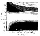
DC 밸런싱된 모노폴라 펄스들이 셀에 인가되었고, 투과도의 효과가 기록되었다. 각 테스트 펄스는 진폭이 V이고, 기간이 τ이었고, 그 뒤를 이어 진폭이 V의 약 5%이고 기간이 20배 길어진 반대 극성의 또 다른 펄스가 인가되었다. 두번째 펄스는 너무 작아서 스위칭을 유발하지 않으나, 많은 테스트 펄스들 후에 셀에 전하가 쌓이는 것을 방지하였다. 도 5와 도6은 펄스 길이와 진폭의 함수인 투과도의 변화를 도시한다. 도 5는 높은 에너지 상태로부터 낮은 에너지 상태로의 스위칭 결과를 도시하고, 도 6은 반대 방향의 스위칭 결과를 나타낸다. 블랙은, 투과도가 변화하여 셀이 스위칭된 것을 지시한다. 화이트는, 투과도의 변화가 없으며 따라서 스위칭이 일어나지 않았음을 나타낸다. DC balanced monopolar pulses were applied to the cell and the effect of transmittance was recorded. Each test pulse had an amplitude of V and a period of τ followed by another pulse of opposite polarity with an amplitude of about 5% of V and a period of 20 times longer. The second pulse was so small that it did not cause switching, but it prevented charge buildup in the cell after many test pulses. 5 and 6 show changes in transmittance as a function of pulse length and amplitude. 5 shows the switching result from the high energy state to the low energy state, and FIG. 6 shows the switching result in the opposite direction. The black indicates that the transmittance has changed and the cell has been switched. White indicates that there is no change in transmittance and therefore no switching occurs.
높은 에너지 상태로부터 낮은 에너지 상태로의 스위칭은, 일반적으로 사인(sign)에 무관하게 유전율 비등방성을 통해 이러한 방향의 스위칭이 발생함을 나타낸다. 반대 방향의 스위칭은 사인에 따르는데, 이는 스위칭이 선형적인 전자- 광학 효과에 의해 조정된다는 것을 나타낸다. 본 발명자들은 이것이 플렉소일렉트릭 효과 (flexoelectric effect)일 것이라고 생각한다. 도 5에서, 비-스위칭 영역은 도 6의 스위칭 영역과 일치한다. 이것은 높은 에너지 상태로부터 낮은 에너지 상태로의 스위칭이 플렉소일렉트릭 효과에 의해 방해된다는 것을 시사한다. Switching from a high energy state to a low energy state generally indicates that switching in this direction occurs through dielectric anisotropy, irrespective of the sign. Switching in the opposite direction depends on the sine, which indicates that the switching is adjusted by a linear electro-optical effect. The inventors believe that this is a flexoelectric effect. In FIG. 5, the non-switching region coincides with the switching region of FIG. 6. This suggests that switching from a high energy state to a low energy state is hampered by the flexoelectric effect.
일련의 추가 실험들에서, 본 발명자들은 셀 파라메터들을 변화시켜 장치의 스위칭 특성들을 최적화시켰다. 바람직한 셀 구조는 셀 간격이 3㎛, 포스트 사이즈 1㎛, 포스트의 사선들중 하나를 따른 오프셋 각도 5°, 1.1㎛ s1813 코팅, N65 초기 농도 3%인 것이 바람직하다.In a further series of experiments, we changed cell parameters to optimize the switching characteristics of the device. Preferred cell structures have a cell spacing of 3 μm, a post size of 1 μm, an offset angle of 5 ° along one of the diagonal lines of the post, 1.1 μm s1813 coating, N65 initial concentration of 3%.
<포스트 어레이들의 SEM 연구>SEM Study of Post Arrays
사각형들로 된 적합한 패턴들을 구비한 마스크들을 사용하여 형성된 실험적 포스트 어레이들의 SEM들은 도 7 내지 도 10에 도시되어 있다. 도 7 및 도 8의 포스트들은 0.7㎛ 사각형 불투명 영역들, 90% s1813, 및 5°의 오프셋 각도를 사용하여 형성되었다. 민감한 독자들은 0.7㎛ "사각형" 포스트들이 사각형이지 않고 대체로 둥근 최상면을 가짐을 주시할 것이다. 포스트들의 기부들은 포스트들의 최상면들보다 덜 둥글다. 이것은 현상 공정으로 인해 둥글게 되는 것과도 일맥 상통한다. 포스트들의 최상면들은 기부들보다 더 오래 동안 현상제에 노출된다. 그러므로 이들은 침식에 더 민감해진다. 포스트들을 구성하는 노광되지 않은 레지스트도 레지스트에서 어느 정도 유한한 용해성을 가지고, 그 효과는 우선 코너들과 같은 예리한 형상들을 침식할 것이다. 더 큰 포스트들은 훨씬 적게 둥글어지는 것을 나타낸다. 예를 들어, 도 9는 약 2㎛ 포스트들을 나타낸다.SEMs of experimental post arrays formed using masks with suitable patterns of squares are shown in FIGS. 7-10. The posts of FIGS. 7 and 8 were formed using 0.7 μm square opaque regions, 90% s1813, and an offset angle of 5 °. Sensitive readers will note that the 0.7 μm “rectangular” posts are not square and have a generally round top surface. The bases of the posts are less round than the tops of the posts. This is in line with the rounding caused by the development process. The top surfaces of the posts are exposed to the developer for longer than the bases. Therefore, they are more sensitive to erosion. The unexposed resist that makes up the posts also has some finite solubility in the resist, and the effect will first erode sharp shapes such as corners. Larger posts show much less rounding. For example, FIG. 9 shows about 2 μm posts.
도 7과 도 8에서 특히 명백한 다른 특징은 포스트들의 측면들의 물결 무늬 형세이다. 이것은 이 포스트들의 어레이들이 442nm 레이저 빔에 의해 노광되었기 때문에, 기판으로부터 반사된 광의 간섭에 기인한 것으로 생각된다. 이 효과는, 인코히어런트한 다수의 파장들을 방출하는 UV 램프를 사용하는 마스크 얼라이너로 노광된 그레이팅들(gratings)에서 보다 덜 명백해져서, 임의의 간섭 효과를 감소시킨다. 이 물결 무늬 형세들은 스위칭에 영향으로 주지 않는 것으로 보인다. Another feature that is particularly apparent in FIGS. 7 and 8 is the moire pattern of the sides of the posts. This is thought to be due to the interference of light reflected from the substrate since these arrays of posts were exposed by a 442 nm laser beam. This effect is less apparent in gratings exposed with a mask aligner using a UV lamp that emits incoherent multiple wavelengths, thereby reducing any interference effect. These wave patterns do not appear to affect switching.
SEM들로부터 흥미로운 또 다른 특징은, 가장 블래이즈된 포스트들에서도 오버행(overhang)들이 없다는 것이다. 예를 들어, 도 10은 심각한 오버행없이 30도에서 노광된 약 0.7㎛의 포스트들을 나타낸다. 본 발명자들은 오버행들이 현상제에 의한 침식에 매우 민감할 것으로 생각한다. Another interesting feature from SEMs is that there are no overhangs even in the most blazed posts. For example, FIG. 10 shows posts of about 0.7 μm exposed at 30 degrees without significant overhang. The inventors believe that overhangs are very sensitive to erosion by the developer.
<둥글어진 포스트들을 사용한 컴퓨터 시뮬레이션>Computer simulation with rounded posts
본 발명자들은 도 7과 도 8의 둥글어진 0.7㎛의 포스트들과 매우 유사하게 보이는 컴퓨터 모델들을 만들었다. 비록 포스트들은, 본 발명자들이 이전의 시뮬레이션들에서 사용했던 이상적인 사각형 포스트들과는 다르지만, 더 실제적인 포스트들 역시 블래이즈된 사선들을 따라 얼라인된, 그러나 두개의 다른 틸트 크기들을 갖는, 여전히 같은 상태들을 제공한다. 이 두 상태들의 에너지들은 이전보다 약간 더 낮으나, 틸트된 상태가 여전히 최저 에너지를 갖는다. 포스트들이 예리한 에지들을 갖는 것은 필수적이지 않은 것으로 보인다. 두개의 상태들은, LC가 포스트 주위에서 비틀어지는 방법 때문에 (앞서 논의한 바와 같이) 발생하는 것으로 생각된다. 이것은 포스트의 단면 모양이 무엇이든지 맞을 것이다. 원통형 포스트들도 마찬가지의 두개의 제니셜(zenithal) 배향들을 줄 것이다. 그러나, 원통형 대칭성 때문에, LC의 방위각 배향을 고정시킬 것이 없고, 모든 방향들이 축퇴될 것이다. 포스트들은 이러한 축퇴를 제거하기 위해 다소의 비대칭성을 가질 필요가 있다. 이것은 예를 들면 소량의 블래이즈(blaze)를 갖는 타원형, 다이아몬드형, 또는 사각형 단면일 수 있다. We have made computer models that look very similar to the rounded 0.7 μm posts of FIGS. 7 and 8. Although the posts differ from the ideal square posts we used in previous simulations, the more practical posts are still aligned with blazed diagonal lines, but still have the same states, with two different tilt sizes. do. The energies of these two states are slightly lower than before, but the tilted state still has the lowest energy. It does not seem necessary for the posts to have sharp edges. Both states are thought to occur (as discussed above) due to the way the LC is twisted around the post. This will fit whatever the cross-sectional shape of the post is. Cylindrical posts will give the same two zenithal orientations. However, due to the cylindrical symmetry there is nothing to fix the azimuthal orientation of the LC and all directions will be degenerate. Posts need to have some asymmetry to eliminate this degeneration. This can be for example an oval, diamond or rectangular cross section with a small amount of blaze.
<포스트들에 의한 수직 배향의 컴퓨터 시뮬레이션>Computer simulation of vertical orientation by posts
본 발명자들은 포스트들에 의한 수직 배향의 컴퓨터 시뮬레이션을 수행하였다. 본 발명자들은 하나의 기판상에 300nm에 걸쳐 있는 사각형 포스트들의 어레이를 갖고, 다른 기판은 플랫한 3㎛의 두꺼운 셀을 모델링했다. 그러나, 재료는 강한 평면 배향을 제공할 것으로서 모델링되었다. 본 발명자들은, LC가 포스트들 주위에서 수직 배향을 채택하는 경우를 살펴보기 위해, 다양한 포스트 높이들과 간격들을 모델링하였다. 도 11은 하부 기판상의 키가 약 1.8㎛인 하나의 포스트를 포함한 영역의 컴퓨터 시뮬레이션 측면도를 나타낸다. 포스트 주위에는 LC가 강하게 틸트되어 있고, 포스트 위에서는, 상부 기판과의 상호 작용에 기인하여 배향이 더 플래너하다. We performed a computer simulation of the vertical orientation by the posts. We have an array of rectangular posts spanning 300 nm on one substrate and the other substrate modeled a flat 3 μm thick cell. However, the material was modeled as providing a strong planar orientation. We modeled various post heights and spacings to see if the LC adopts a vertical orientation around the posts. FIG. 11 shows a computer simulated side view of an area containing one post about 1.8 μm tall on the lower substrate. The LC is strongly tilted around the post, and on the post, the orientation is more planar due to interaction with the upper substrate.
컴퓨터 시뮬레이션들에서, 본 발명자들은 포스트 높이를 0.2로부터 2.6㎛까지 변화시키고, 포스트들 간의 갭을 0.6으로부터 1.2㎛까지 변화시키는 효과를 모델링했다. 포스트 높이가 증가됨에 따라, 배향은 단순한 플래너인 것으로부터 플래너 상태와 더 틸트된 상태 사이의 쌍안정 또는 다중 안정인 것으로 변한다. 포스트 높이가 더 증가됨에 따라, 플래너 상태가 에너지가 너무 높게 되어, 단지 많이 틸트된 수직 상태가 있게 된다. 본 연구는, 포스트 높이가 대략 평균 포스트 간격과 같은 때부터 수직 배향이 시작함을 나타낸다. 이 효과는 매우 작은 단면의 포스트들에 대해서는 낮아질 것으로 기대된다. 수직 배향에 대한 포스트 단면의 예상되는 상한은 포스트 폭이 셀 간격 수준일 때이다. In computer simulations, we modeled the effect of changing the post height from 0.2 to 2.6 μm and the gap between the posts from 0.6 to 1.2 μm. As the post height is increased, the orientation changes from being a simple planner to bistable or multiple stable between the planar state and the more tilted state. As the post height is further increased, the planar state becomes too high in energy, leaving only a much tilted vertical state. This study shows that the vertical orientation starts when the post height is approximately equal to the average post spacing. This effect is expected to be low for posts of very small cross section. The expected upper limit of the post cross section for the vertical orientation is when the post width is at the cell gap level.
도 12는 등변 삼각형인 단면 모양을 갖는 포스트 주위의 LC 배향의 컴퓨터-생성 모델을 도시한다. 이 모델은, 도시된 도면이 사각형 어레이의 사각형 단위 셀이라고 가정한다. 사각형의 각 변의 길이는 약 1.5㎛이다. 포스트는 대략 1:1의 어스펙트 비를 갖는 비교적 얇은 것으로 모델링된다. 각 삼각형의 이등분선들은 사각형 어레이의 변들과 평행한 축들에 대해 20°로 얼라인된다. 로컬 액정 방향자는 도 12a 내지 도 12c에 예시한 바와 같은 세개의 방위각 방향들중의 하나를 채택할 수 있다. 12 shows a computer-generated model of LC orientation around a post having a cross-sectional shape that is equilateral triangle. This model assumes that the illustrated figure is a rectangular unit cell of a rectangular array. Each side of the square is about 1.5 mu m in length. Posts are modeled as relatively thin with an aspect ratio of approximately 1: 1. The bisectors of each triangle are aligned at 20 ° with respect to the axes parallel to the sides of the rectangular array. The local liquid crystal director may adopt one of three azimuth directions as illustrated in FIGS. 12A-12C.
LC 방향자의 방위는 원칙적으로는 도 13에 가장 잘 예시된 바와 같이 포스트들의 형태와 방향에 의해 결정된다. 도 13은 도 12에 도시된 바와 동일한 디멘젼들을 갖는 사각형 어레이의 사각형 단위 셀들을 도시한다. 포스트들은 단면이 타원이다. 도 13a에서, 타원의 장축은 어레이의 축들중 하나와 평행한 것으로 모델링된다. 도 13b 내지 도 13d는 포스트들이 15°, 30°, 45°로 각각 회전될 때 LC 방향자의 방향에 어떠한 영향을 주는 지를 나타낸다. 도 13a에서, 방향자는 타원의 장축을 따라 그리고 어레이의 축을 따라 얼라인된다. 비록 어레이로부터의 다소 약한 배향 효과가 15°와 30°의 포스트 배향들에서 보여지지만, 포스트들의 점차적인 회전은 LC 방향자의 점차적인 회전을 유발한다. 방향자 배향은 주로 포스트들의 형태와 방향에 의해 결정된다. 도 4에 도시된 예에서와 같이, 포스트들을 의사랜덤 어레이로 배열함으로써, 어레이의 효과들이 상쇄될 수 있다. The orientation of the LC director is in principle determined by the shape and direction of the posts as best illustrated in FIG. 13. FIG. 13 shows rectangular unit cells in a rectangular array with the same dimensions as shown in FIG. 12. The posts are elliptical in cross section. In FIG. 13A, the long axis of the ellipse is modeled as parallel to one of the axes of the array. 13b to 13d show how the posts are affected in the direction of the LC director when they are rotated 15 °, 30 ° and 45 °, respectively. In FIG. 13A, the director is aligned along the long axis of the ellipse and along the axis of the array. Although a rather weak orientation effect from the array is seen at post orientations of 15 ° and 30 °, the gradual rotation of the posts causes a gradual rotation of the LC director. The director orientation is mainly determined by the shape and direction of the posts. As in the example shown in FIG. 4, by arranging the posts in a pseudorandom array, the effects of the array can be canceled.
도 14 내지 도 18은 본 발명의 대안적인 실시예들에 따른 장치들의 포스트들의 사시도들이다. 도 14에서, 타원형 포스트들은 규칙적인 어레이로 배열된다. 포스트들은 모두 같은 높이이고 그들의 장축들이 서로 평행하게 배열된다. 어스팩트 비에 따라, 이것은 단일 방위각 방향으로의 균일한 방향자 배향을 생성한다. 그들의 높이에 따라, 포스트들은 균일한 플래너 배향이나, 쌍안정 또는 다중 안정 배향 (평면 또는 틸트형), 또는 수직 배향 (틸트될 수 있음)를 생성할 수 있다. 도 15의 포스트들도 유사하나 랜덤 어레이로 배열되어 있고, 랜덤 어레이는 간섭 효과들을 거의 제거한다. 포스트들은 도 20에 도시된 바와 같이, 불균일한 단면을 가질 수 있다. 또는 포스트들은 도 19에 예시된 바와 같이 오버행을 가질 수 있다. 도 16에서, 포스트들은 규칙적인 어레이로 배열되지만, 상이한 영역들에서 상이한 높이들을 갖는다. 이것은 포스트들이 더 높은 영역들에서 더 높은 틸트를 초래할 것이고, 이에 따라 상이한 광학 효과들을 가져온다. 도 17에서, 타원형 포스트들은 랜덤하게 방위가 지어져서, 네마틱 방향자의 롱 레인지 방위가 강하게 편향되지 않는 배향 구조를 제공한다. 이 구조와 이와 유사한 다른 구조들이 양의 유전율 이방성을 갖는 LC 재료과 함께 산란 모드의 디스플레이에 사용될 수 있을 것으로 예상된다. 도 18은 상이한 영역들에서 제어된 배향을 주도록 사용될 수 있는 복수의 형태들과 사이즈들을 갖는 포스트들의 배열, 및 그레이스케일과 같은 다른 효과들을 나타낸다. 도 19의 포스트들은 디스플레이의 상이한 영역들에서 상이한 각도로 틸트되어 있어서, 예를 들어 HAN 모드에서, LC 배향에 상이한 틸트각과, 그레이스케일을 생성할 가능성을 제공한다. 14-18 are perspective views of posts of devices in accordance with alternative embodiments of the present invention. In FIG. 14, elliptical posts are arranged in a regular array. The posts are all the same height and their major axes are arranged parallel to each other. Depending on the aspect ratio, this produces a uniform director orientation in a single azimuthal direction. Depending on their height, the posts may produce a uniform planar orientation, bistable or multiple stable orientations (planar or tilted), or vertical orientations (which may be tilted). The posts of FIG. 15 are similar but arranged in a random array, which randomly eliminates interference effects. The posts may have a non-uniform cross section, as shown in FIG. 20. Or the posts may have an overhang as illustrated in FIG. 19. In FIG. 16, the posts are arranged in a regular array, but with different heights in different regions. This will result in higher tilt in the posts where they are higher, resulting in different optical effects. In FIG. 17, the elliptical posts are randomly oriented, providing an orientation structure in which the long range orientation of the nematic director is not strongly deflected. It is anticipated that this structure and other similar structures can be used for display in scattering mode with LC materials having positive dielectric anisotropy. 18 illustrates an arrangement of posts having a plurality of shapes and sizes that can be used to give a controlled orientation in different areas, and other effects such as grayscale. The posts of FIG. 19 are tilted at different angles in different areas of the display, giving the possibility of generating different tilt angles and grayscales in the LC orientation, for example in HAN mode.
본 발명에 따르면, 보다 제어 가능하게 제조 가능한 LC 장치들용의 배향이 제공된다.According to the present invention, an orientation for more controllable LC devices is provided.
Claims (22)
Applications Claiming Priority (2)
| Application Number | Priority Date | Filing Date | Title |
|---|---|---|---|
| EP00302478.3 | 2000-03-27 | ||
| EP00302478A EP1139150A1 (en) | 2000-03-27 | 2000-03-27 | Liquid crystal alignment structure |
Publications (2)
| Publication Number | Publication Date |
|---|---|
| KR20010090587A KR20010090587A (en) | 2001-10-18 |
| KR100794889B1 true KR100794889B1 (en) | 2008-01-14 |
Family
ID=8172826
Family Applications (1)
| Application Number | Title | Priority Date | Filing Date |
|---|---|---|---|
| KR1020010015982A KR100794889B1 (en) | 2000-03-27 | 2001-03-27 | Liquid crystal alignment |
Country Status (5)
| Country | Link |
|---|---|
| US (2) | US7397526B2 (en) |
| EP (1) | EP1139150A1 (en) |
| JP (1) | JP4801272B2 (en) |
| KR (1) | KR100794889B1 (en) |
| DE (1) | DE60128507T2 (en) |
Families Citing this family (8)
| Publication number | Priority date | Publication date | Assignee | Title |
|---|---|---|---|---|
| EP1139150A1 (en) * | 2000-03-27 | 2001-10-04 | Hewlett-Packard Company, A Delaware Corporation | Liquid crystal alignment structure |
| EP1271225A1 (en) * | 2001-06-22 | 2003-01-02 | Hewlett-Packard Company, A Delaware Corporation | Bistable nematic liquid crystal device |
| US7929094B2 (en) * | 2004-04-22 | 2011-04-19 | Sharp Kabushiki Kaisha | Vertically-aligned liquid crystal display device having a rugged structure which is in contact with the liquid crystal layer |
| KR101097677B1 (en) * | 2010-06-01 | 2011-12-22 | 서울대학교산학협력단 | Liquid crystal display device, method for manufacturing the same and method for manufacturing substrate for alignment of liquid crystal |
| US11067860B2 (en) | 2016-11-18 | 2021-07-20 | Magic Leap, Inc. | Liquid crystal diffractive devices with nano-scale pattern and methods of manufacturing the same |
| WO2018094079A1 (en) | 2016-11-18 | 2018-05-24 | Magic Leap, Inc. | Spatially variable liquid crystal diffraction gratings |
| US11262495B1 (en) | 2017-10-04 | 2022-03-01 | Facebook Technologies, Llc | Waveguides with high refractive index gratings manufactured by post-patterning infusion |
| US11035988B1 (en) * | 2018-05-22 | 2021-06-15 | Facebook Technologies, Llc | Tunable shrinkage process for manufacturing gratings |
Citations (4)
| Publication number | Priority date | Publication date | Assignee | Title |
|---|---|---|---|---|
| JPH0618858A (en) * | 1992-06-30 | 1994-01-28 | Matsushita Electric Ind Co Ltd | Liquid crystal panel and liquid crystal projection type television using the panel |
| JPH07199168A (en) * | 1993-12-28 | 1995-08-04 | Nec Corp | Liquid crystal optical element |
| JPH0843822A (en) * | 1994-07-29 | 1996-02-16 | Toshiba Corp | Liquid crystal display device |
| KR19990075709A (en) * | 1998-03-24 | 1999-10-15 | 손욱 | LCD and its manufacturing method |
Family Cites Families (49)
| Publication number | Priority date | Publication date | Assignee | Title |
|---|---|---|---|---|
| JPS542580B2 (en) * | 1974-07-01 | 1979-02-09 | ||
| US4294782A (en) | 1979-04-10 | 1981-10-13 | Jerome Bauer | Method for substantially instantaneous liquid molding of an article |
| US4333708A (en) | 1979-11-30 | 1982-06-08 | Bell Telephone Laboratories, Incorporated | Mechanically multistable liquid crystal cell |
| JPS56138712A (en) * | 1980-03-31 | 1981-10-29 | Citizen Watch Co Ltd | Color liquid crystal display device |
| US4906315A (en) | 1983-06-20 | 1990-03-06 | Mcgrew Stephen P | Surface relief holograms and holographic hot-stamping foils, and method of fabricating same |
| US4758296A (en) | 1983-06-20 | 1988-07-19 | Mcgrew Stephen P | Method of fabricating surface relief holograms |
| JPS60217339A (en) * | 1984-04-13 | 1985-10-30 | Matsushita Electric Ind Co Ltd | Liquid crystal display panel and its manufacture |
| JPS61269122A (en) * | 1985-05-24 | 1986-11-28 | Canon Inc | Liquid crystal focusing plate |
| GB8608276D0 (en) | 1986-04-04 | 1986-05-08 | British Telecomm | Optical devices |
| US4996123A (en) * | 1986-07-11 | 1991-02-26 | Matsushita Electric Industrial Co., Ltd. | Optically oriented photoresist pattern forming method using organic crystal in photoresist layer with specified refracting indices formula |
| JPH02211422A (en) * | 1989-02-13 | 1990-08-22 | Seiko Epson Corp | Liquid crystal shutter |
| JPH02226115A (en) * | 1989-02-28 | 1990-09-07 | Citizen Watch Co Ltd | Production of ferroelectric liquid crystal element |
| FR2666908B2 (en) | 1990-01-30 | 1992-12-18 | Centre Nat Rech Scient | IMPROVEMENTS ON BISTABLE OPTICAL DEVICES WITH LIQUID CRYSTALS AND ELECTROCHIRAL CONTROL. |
| FR2666923A2 (en) | 1990-06-22 | 1992-03-20 | Centre Nat Rech Scient | Improvements to nematic liquid-crystal displays, with surface bistability, controlled by flexoelectric effect |
| US5327271A (en) | 1990-08-17 | 1994-07-05 | Dainippon Ink And Chemical, Inc. | Liquid crystal device employing polymer network on one substrate and alignment layer or polymer network on other substrate |
| JP3267989B2 (en) * | 1991-08-26 | 2002-03-25 | 株式会社東芝 | Method for manufacturing liquid crystal alignment film |
| JPH0588177A (en) | 1991-09-30 | 1993-04-09 | Toshiba Corp | Liquid crystal display element |
| JP3158607B2 (en) * | 1992-03-10 | 2001-04-23 | セイコーエプソン株式会社 | Liquid crystal display |
| JPH06118416A (en) * | 1992-10-08 | 1994-04-28 | Toyota Motor Corp | Liquid crystal light refraction element |
| JPH06308498A (en) * | 1993-04-22 | 1994-11-04 | Canon Inc | Ferroelectric liquid crystal element |
| US5739889A (en) | 1993-04-27 | 1998-04-14 | Sharp Kabushiki Kaisha | Liquid crystal display device and a production method for the same |
| DE69413624T2 (en) | 1993-07-27 | 1999-05-06 | Sharp Kk | Liquid crystal display device |
| GB9402517D0 (en) * | 1994-02-09 | 1994-03-30 | Secr Defence | Ferroelectric liquid crystal alignment |
| GB9402513D0 (en) | 1994-02-09 | 1994-03-30 | Secr Defence | Bistable nematic liquid crystal device |
| TW428116B (en) | 1994-05-18 | 2001-04-01 | Matsushita Electric Ind Co Ltd | Liquid crystal display element and laminated phase difference plate used for the same |
| KR0148669B1 (en) | 1994-06-24 | 1998-11-16 | 가다오까 마사다까 | Liquid crystal device and method of preparing the same, method of preparing liquid crystal oriented film, mold for preparing liquid crystal oriented film and the method of preparing the same, apparatus for transfering a pattern on the oriented film |
| GB9502635D0 (en) * | 1995-02-10 | 1995-03-29 | Secr Defence | Liquid crystal device alignment |
| US5552611A (en) | 1995-06-06 | 1996-09-03 | International Business Machines | Pseudo-random registration masks for projection lithography tool |
| JP3298607B2 (en) * | 1995-09-29 | 2002-07-02 | ソニー株式会社 | Liquid crystal element and manufacturing method thereof |
| JPH09105941A (en) | 1995-10-13 | 1997-04-22 | Stanley Electric Co Ltd | Liquid crystal display device |
| GB9521106D0 (en) * | 1995-10-16 | 1995-12-20 | Secr Defence | Bistable nematic liquid crystal device |
| US6236445B1 (en) | 1996-02-22 | 2001-05-22 | Hughes Electronics Corporation | Method for making topographic projections |
| GB9607854D0 (en) * | 1996-04-16 | 1996-06-19 | Secr Defence | Liquid crystal device |
| JPH10213794A (en) * | 1996-04-30 | 1998-08-11 | Nec Corp | Liquid crystal display device |
| JP3199677B2 (en) | 1997-11-20 | 2001-08-20 | セイコーエプソン株式会社 | Manufacturing method of electro-optical device |
| JPH11160706A (en) * | 1997-11-21 | 1999-06-18 | Stanley Electric Co Ltd | Production of liquid crystal display element |
| GB9727142D0 (en) | 1997-12-24 | 1998-02-25 | Secr Defence | Bistable nematic liquid crystal device |
| JP3481843B2 (en) | 1997-12-26 | 2003-12-22 | シャープ株式会社 | Liquid crystal display |
| JP3977513B2 (en) * | 1998-04-28 | 2007-09-19 | 東レ株式会社 | Divided alignment substrate and liquid crystal display device using the same |
| JP3335578B2 (en) * | 1998-06-30 | 2002-10-21 | シャープ株式会社 | Liquid crystal display device and manufacturing method thereof |
| JP2000105376A (en) * | 1998-09-29 | 2000-04-11 | Sharp Corp | Liquid crystal display device |
| US6519018B1 (en) * | 1998-11-03 | 2003-02-11 | International Business Machines Corporation | Vertically aligned liquid crystal displays and methods for their production |
| JP2000206535A (en) | 1999-01-12 | 2000-07-28 | Sony Corp | Transmissive hybrid aligned liquid crystal display device |
| EP1028346A3 (en) | 1999-02-12 | 2002-05-02 | Matsushita Electric Industrial Co., Ltd. | Liquid crystal element and manufacturing method thereof |
| EP1094103A1 (en) | 1999-10-19 | 2001-04-25 | Rolic AG | Topologically structured polymer coating |
| GB9928126D0 (en) | 1999-11-30 | 2000-01-26 | Secr Defence | Bistable nematic liquid crystal device |
| EP1139152A1 (en) * | 2000-03-27 | 2001-10-04 | Hewlett-Packard Company, A Delaware Corporation | Liquid crystal alignment structure |
| EP1139150A1 (en) * | 2000-03-27 | 2001-10-04 | Hewlett-Packard Company, A Delaware Corporation | Liquid crystal alignment structure |
| US6472237B1 (en) | 2001-10-26 | 2002-10-29 | Motorola, Inc. | Method and system for determining a thickness of a layer |
-
2000
- 2000-03-27 EP EP00302478A patent/EP1139150A1/en not_active Withdrawn
-
2001
- 2001-02-22 DE DE60128507T patent/DE60128507T2/en not_active Expired - Lifetime
- 2001-03-23 US US09/816,941 patent/US7397526B2/en not_active Expired - Fee Related
- 2001-03-27 JP JP2001090214A patent/JP4801272B2/en not_active Expired - Fee Related
- 2001-03-27 KR KR1020010015982A patent/KR100794889B1/en not_active IP Right Cessation
-
2008
- 2008-08-06 US US12/221,820 patent/US7633596B2/en not_active Expired - Fee Related
Patent Citations (4)
| Publication number | Priority date | Publication date | Assignee | Title |
|---|---|---|---|---|
| JPH0618858A (en) * | 1992-06-30 | 1994-01-28 | Matsushita Electric Ind Co Ltd | Liquid crystal panel and liquid crystal projection type television using the panel |
| JPH07199168A (en) * | 1993-12-28 | 1995-08-04 | Nec Corp | Liquid crystal optical element |
| JPH0843822A (en) * | 1994-07-29 | 1996-02-16 | Toshiba Corp | Liquid crystal display device |
| KR19990075709A (en) * | 1998-03-24 | 1999-10-15 | 손욱 | LCD and its manufacturing method |
Also Published As
| Publication number | Publication date |
|---|---|
| KR20010090587A (en) | 2001-10-18 |
| DE60128507D1 (en) | 2007-07-05 |
| US20090073373A1 (en) | 2009-03-19 |
| US7397526B2 (en) | 2008-07-08 |
| DE60128507T2 (en) | 2008-03-06 |
| JP4801272B2 (en) | 2011-10-26 |
| US7633596B2 (en) | 2009-12-15 |
| EP1139150A1 (en) | 2001-10-04 |
| JP2001281660A (en) | 2001-10-10 |
| US20010024256A1 (en) | 2001-09-27 |
Similar Documents
| Publication | Publication Date | Title |
|---|---|---|
| US7106410B2 (en) | Bistable nematic liquid crystal device comprising an array of upstanding alignment posts | |
| US7460200B2 (en) | Liquid crystal alignment | |
| KR100794888B1 (en) | Liquid crystal alignment | |
| EP0744039B1 (en) | Liquid crystal device alignment | |
| US7633596B2 (en) | Liquid crystal alignment | |
| CN1145121A (en) | Bistable nematic liquid crystal devices | |
| JPH10513276A (en) | Liquid crystal device alignment | |
| JP2004505297A (en) | Liquid crystal element | |
| US6992741B2 (en) | Bistable nematic liquid crystal device | |
| EP1139154B1 (en) | Liquid crystal alignment | |
| EP1139153B1 (en) | Liquid crystal alignment | |
| JP5127006B2 (en) | Liquid crystal display element using nematic liquid crystal | |
| KR0182116B1 (en) | Method for controlling alignment direction in liquid crystal cell | |
| EP1271226B1 (en) | Bistable nematic liquid crystal device | |
| EP1091237A1 (en) | Liquid crystal device |
Legal Events
| Date | Code | Title | Description |
|---|---|---|---|
| A201 | Request for examination | ||
| E902 | Notification of reason for refusal | ||
| E701 | Decision to grant or registration of patent right | ||
| GRNT | Written decision to grant | ||
| G170 | Re-publication after modification of scope of protection [patent] | ||
| FPAY | Annual fee payment |
Payment date: 20130102 Year of fee payment: 6 |
|
| FPAY | Annual fee payment |
Payment date: 20140102 Year of fee payment: 7 |
|
| LAPS | Lapse due to unpaid annual fee |