KR100510001B1 - Manufacturing method of semiconductor device - Google Patents
Manufacturing method of semiconductor device Download PDFInfo
- Publication number
- KR100510001B1 KR100510001B1 KR1019970022172A KR19970022172A KR100510001B1 KR 100510001 B1 KR100510001 B1 KR 100510001B1 KR 1019970022172 A KR1019970022172 A KR 1019970022172A KR 19970022172 A KR19970022172 A KR 19970022172A KR 100510001 B1 KR100510001 B1 KR 100510001B1
- Authority
- KR
- South Korea
- Prior art keywords
- region
- substrate
- line
- channel
- irradiated
- Prior art date
Links
- 239000004065 semiconductor Substances 0.000 title claims description 23
- 238000004519 manufacturing process Methods 0.000 title claims description 8
- 239000000758 substrate Substances 0.000 claims abstract description 51
- 238000000034 method Methods 0.000 claims description 11
- 230000003287 optical effect Effects 0.000 claims description 8
- 230000010355 oscillation Effects 0.000 claims description 3
- 238000007493 shaping process Methods 0.000 claims 1
- 238000002425 crystallisation Methods 0.000 abstract description 23
- 230000008025 crystallization Effects 0.000 abstract description 23
- 238000005224 laser annealing Methods 0.000 abstract description 7
- 230000009467 reduction Effects 0.000 abstract description 5
- 239000013256 coordination polymer Substances 0.000 abstract description 3
- 239000013078 crystal Substances 0.000 abstract description 2
- 230000006866 deterioration Effects 0.000 abstract 1
- 239000010408 film Substances 0.000 description 15
- 229910021417 amorphous silicon Inorganic materials 0.000 description 10
- 239000010410 layer Substances 0.000 description 10
- 239000011159 matrix material Substances 0.000 description 9
- 230000002950 deficient Effects 0.000 description 8
- 239000011521 glass Substances 0.000 description 7
- 239000004973 liquid crystal related substance Substances 0.000 description 6
- 230000008569 process Effects 0.000 description 6
- 238000010586 diagram Methods 0.000 description 5
- 238000009826 distribution Methods 0.000 description 5
- 239000011229 interlayer Substances 0.000 description 5
- 239000003513 alkali Substances 0.000 description 4
- 230000002093 peripheral effect Effects 0.000 description 4
- 238000000137 annealing Methods 0.000 description 3
- 239000003990 capacitor Substances 0.000 description 2
- 239000012535 impurity Substances 0.000 description 2
- 230000007257 malfunction Effects 0.000 description 2
- 229910052751 metal Inorganic materials 0.000 description 2
- 239000002184 metal Substances 0.000 description 2
- VYPSYNLAJGMNEJ-UHFFFAOYSA-N Silicium dioxide Chemical compound O=[Si]=O VYPSYNLAJGMNEJ-UHFFFAOYSA-N 0.000 description 1
- XUIMIQQOPSSXEZ-UHFFFAOYSA-N Silicon Chemical compound [Si] XUIMIQQOPSSXEZ-UHFFFAOYSA-N 0.000 description 1
- 230000009471 action Effects 0.000 description 1
- 238000003491 array Methods 0.000 description 1
- 230000015572 biosynthetic process Effects 0.000 description 1
- 230000000903 blocking effect Effects 0.000 description 1
- 230000008859 change Effects 0.000 description 1
- 230000000295 complement effect Effects 0.000 description 1
- 230000003247 decreasing effect Effects 0.000 description 1
- 230000007547 defect Effects 0.000 description 1
- 230000005669 field effect Effects 0.000 description 1
- 238000002347 injection Methods 0.000 description 1
- 239000007924 injection Substances 0.000 description 1
- 238000005468 ion implantation Methods 0.000 description 1
- 230000001678 irradiating effect Effects 0.000 description 1
- 238000000465 moulding Methods 0.000 description 1
- 230000003071 parasitic effect Effects 0.000 description 1
- 229910021420 polycrystalline silicon Inorganic materials 0.000 description 1
- 238000001953 recrystallisation Methods 0.000 description 1
- 229910052710 silicon Inorganic materials 0.000 description 1
- 239000010703 silicon Substances 0.000 description 1
- 229910052709 silver Inorganic materials 0.000 description 1
- 239000004332 silver Substances 0.000 description 1
- 239000007790 solid phase Substances 0.000 description 1
- 239000010409 thin film Substances 0.000 description 1
- 229910052721 tungsten Inorganic materials 0.000 description 1
- WQJQOUPTWCFRMM-UHFFFAOYSA-N tungsten disilicide Chemical compound [Si]#[W]#[Si] WQJQOUPTWCFRMM-UHFFFAOYSA-N 0.000 description 1
- 229910021342 tungsten silicide Inorganic materials 0.000 description 1
Images


Classifications
-
- H—ELECTRICITY
- H01—ELECTRIC ELEMENTS
- H01L—SEMICONDUCTOR DEVICES NOT COVERED BY CLASS H10
- H01L21/00—Processes or apparatus adapted for the manufacture or treatment of semiconductor or solid state devices or of parts thereof
- H01L21/02—Manufacture or treatment of semiconductor devices or of parts thereof
- H01L21/02104—Forming layers
- H01L21/02365—Forming inorganic semiconducting materials on a substrate
- H01L21/02656—Special treatments
- H01L21/02664—Aftertreatments
- H01L21/02667—Crystallisation or recrystallisation of non-monocrystalline semiconductor materials, e.g. regrowth
- H01L21/02675—Crystallisation or recrystallisation of non-monocrystalline semiconductor materials, e.g. regrowth using laser beams
-
- G—PHYSICS
- G02—OPTICS
- G02F—OPTICAL DEVICES OR ARRANGEMENTS FOR THE CONTROL OF LIGHT BY MODIFICATION OF THE OPTICAL PROPERTIES OF THE MEDIA OF THE ELEMENTS INVOLVED THEREIN; NON-LINEAR OPTICS; FREQUENCY-CHANGING OF LIGHT; OPTICAL LOGIC ELEMENTS; OPTICAL ANALOGUE/DIGITAL CONVERTERS
- G02F1/00—Devices or arrangements for the control of the intensity, colour, phase, polarisation or direction of light arriving from an independent light source, e.g. switching, gating or modulating; Non-linear optics
- G02F1/01—Devices or arrangements for the control of the intensity, colour, phase, polarisation or direction of light arriving from an independent light source, e.g. switching, gating or modulating; Non-linear optics for the control of the intensity, phase, polarisation or colour
- G02F1/13—Devices or arrangements for the control of the intensity, colour, phase, polarisation or direction of light arriving from an independent light source, e.g. switching, gating or modulating; Non-linear optics for the control of the intensity, phase, polarisation or colour based on liquid crystals, e.g. single liquid crystal display cells
- G02F1/133—Constructional arrangements; Operation of liquid crystal cells; Circuit arrangements
- G02F1/1333—Constructional arrangements; Manufacturing methods
- G02F1/1345—Conductors connecting electrodes to cell terminals
- G02F1/13454—Drivers integrated on the active matrix substrate
-
- G—PHYSICS
- G02—OPTICS
- G02F—OPTICAL DEVICES OR ARRANGEMENTS FOR THE CONTROL OF LIGHT BY MODIFICATION OF THE OPTICAL PROPERTIES OF THE MEDIA OF THE ELEMENTS INVOLVED THEREIN; NON-LINEAR OPTICS; FREQUENCY-CHANGING OF LIGHT; OPTICAL LOGIC ELEMENTS; OPTICAL ANALOGUE/DIGITAL CONVERTERS
- G02F1/00—Devices or arrangements for the control of the intensity, colour, phase, polarisation or direction of light arriving from an independent light source, e.g. switching, gating or modulating; Non-linear optics
- G02F1/01—Devices or arrangements for the control of the intensity, colour, phase, polarisation or direction of light arriving from an independent light source, e.g. switching, gating or modulating; Non-linear optics for the control of the intensity, phase, polarisation or colour
- G02F1/13—Devices or arrangements for the control of the intensity, colour, phase, polarisation or direction of light arriving from an independent light source, e.g. switching, gating or modulating; Non-linear optics for the control of the intensity, phase, polarisation or colour based on liquid crystals, e.g. single liquid crystal display cells
- G02F1/133—Constructional arrangements; Operation of liquid crystal cells; Circuit arrangements
- G02F1/136—Liquid crystal cells structurally associated with a semi-conducting layer or substrate, e.g. cells forming part of an integrated circuit
- G02F1/1362—Active matrix addressed cells
- G02F1/136204—Arrangements to prevent high voltage or static electricity failures
-
- H—ELECTRICITY
- H01—ELECTRIC ELEMENTS
- H01L—SEMICONDUCTOR DEVICES NOT COVERED BY CLASS H10
- H01L21/00—Processes or apparatus adapted for the manufacture or treatment of semiconductor or solid state devices or of parts thereof
- H01L21/02—Manufacture or treatment of semiconductor devices or of parts thereof
- H01L21/02104—Forming layers
- H01L21/02365—Forming inorganic semiconducting materials on a substrate
- H01L21/02367—Substrates
- H01L21/0237—Materials
- H01L21/02422—Non-crystalline insulating materials, e.g. glass, polymers
-
- H—ELECTRICITY
- H01—ELECTRIC ELEMENTS
- H01L—SEMICONDUCTOR DEVICES NOT COVERED BY CLASS H10
- H01L21/00—Processes or apparatus adapted for the manufacture or treatment of semiconductor or solid state devices or of parts thereof
- H01L21/02—Manufacture or treatment of semiconductor devices or of parts thereof
- H01L21/02104—Forming layers
- H01L21/02365—Forming inorganic semiconducting materials on a substrate
- H01L21/02518—Deposited layers
- H01L21/02521—Materials
- H01L21/02524—Group 14 semiconducting materials
- H01L21/02532—Silicon, silicon germanium, germanium
-
- H—ELECTRICITY
- H01—ELECTRIC ELEMENTS
- H01L—SEMICONDUCTOR DEVICES NOT COVERED BY CLASS H10
- H01L21/00—Processes or apparatus adapted for the manufacture or treatment of semiconductor or solid state devices or of parts thereof
- H01L21/02—Manufacture or treatment of semiconductor devices or of parts thereof
- H01L21/02104—Forming layers
- H01L21/02365—Forming inorganic semiconducting materials on a substrate
- H01L21/02656—Special treatments
- H01L21/02664—Aftertreatments
- H01L21/02667—Crystallisation or recrystallisation of non-monocrystalline semiconductor materials, e.g. regrowth
- H01L21/02675—Crystallisation or recrystallisation of non-monocrystalline semiconductor materials, e.g. regrowth using laser beams
- H01L21/02678—Beam shaping, e.g. using a mask
-
- H—ELECTRICITY
- H01—ELECTRIC ELEMENTS
- H01L—SEMICONDUCTOR DEVICES NOT COVERED BY CLASS H10
- H01L21/00—Processes or apparatus adapted for the manufacture or treatment of semiconductor or solid state devices or of parts thereof
- H01L21/02—Manufacture or treatment of semiconductor devices or of parts thereof
- H01L21/02104—Forming layers
- H01L21/02365—Forming inorganic semiconducting materials on a substrate
- H01L21/02656—Special treatments
- H01L21/02664—Aftertreatments
- H01L21/02667—Crystallisation or recrystallisation of non-monocrystalline semiconductor materials, e.g. regrowth
- H01L21/02675—Crystallisation or recrystallisation of non-monocrystalline semiconductor materials, e.g. regrowth using laser beams
- H01L21/02686—Pulsed laser beam
-
- H—ELECTRICITY
- H01—ELECTRIC ELEMENTS
- H01L—SEMICONDUCTOR DEVICES NOT COVERED BY CLASS H10
- H01L29/00—Semiconductor devices adapted for rectifying, amplifying, oscillating or switching, or capacitors or resistors with at least one potential-jump barrier or surface barrier, e.g. PN junction depletion layer or carrier concentration layer; Details of semiconductor bodies or of electrodes thereof ; Multistep manufacturing processes therefor
- H01L29/66—Types of semiconductor device ; Multistep manufacturing processes therefor
- H01L29/66007—Multistep manufacturing processes
- H01L29/66075—Multistep manufacturing processes of devices having semiconductor bodies comprising group 14 or group 13/15 materials
- H01L29/66227—Multistep manufacturing processes of devices having semiconductor bodies comprising group 14 or group 13/15 materials the devices being controllable only by the electric current supplied or the electric potential applied, to an electrode which does not carry the current to be rectified, amplified or switched, e.g. three-terminal devices
- H01L29/66409—Unipolar field-effect transistors
- H01L29/66477—Unipolar field-effect transistors with an insulated gate, i.e. MISFET
- H01L29/66742—Thin film unipolar transistors
- H01L29/6675—Amorphous silicon or polysilicon transistors
- H01L29/66757—Lateral single gate single channel transistors with non-inverted structure, i.e. the channel layer is formed before the gate
-
- Y—GENERAL TAGGING OF NEW TECHNOLOGICAL DEVELOPMENTS; GENERAL TAGGING OF CROSS-SECTIONAL TECHNOLOGIES SPANNING OVER SEVERAL SECTIONS OF THE IPC; TECHNICAL SUBJECTS COVERED BY FORMER USPC CROSS-REFERENCE ART COLLECTIONS [XRACs] AND DIGESTS
- Y10—TECHNICAL SUBJECTS COVERED BY FORMER USPC
- Y10S—TECHNICAL SUBJECTS COVERED BY FORMER USPC CROSS-REFERENCE ART COLLECTIONS [XRACs] AND DIGESTS
- Y10S117/00—Single-crystal, oriented-crystal, and epitaxy growth processes; non-coating apparatus therefor
- Y10S117/903—Dendrite or web or cage technique
- Y10S117/904—Laser beam
Landscapes
- Physics & Mathematics (AREA)
- Engineering & Computer Science (AREA)
- General Physics & Mathematics (AREA)
- Microelectronics & Electronic Packaging (AREA)
- Power Engineering (AREA)
- Computer Hardware Design (AREA)
- Condensed Matter Physics & Semiconductors (AREA)
- Manufacturing & Machinery (AREA)
- Chemical & Material Sciences (AREA)
- Optics & Photonics (AREA)
- Crystallography & Structural Chemistry (AREA)
- Nonlinear Science (AREA)
- Mathematical Physics (AREA)
- Ceramic Engineering (AREA)
- Materials Engineering (AREA)
- Thin Film Transistor (AREA)
- Recrystallisation Techniques (AREA)
- Liquid Crystal (AREA)
Abstract
p-Si TFT LCD의 p-Si를 형성하는 레이저 어닐에 있어서 조사 영역의 강도의 불균일함에 기인한 트랜지스터 특성의 악화를 방지한다.In the laser annealing forming p-Si of the p-Si TFT LCD, deterioration of transistor characteristics due to nonuniformity in the intensity of the irradiation area is prevented.
에지 라인이 피처리 기판의 수직 혹은 수평 방향에 대해서 45 °의 방향(S1, S2)으로 되도록 라인 빔을 조사하는 것으로 라인 빔의 강도의 어긋남에 의해 그레인 크기가 충분히 크게 되지 않은 선형(線狀)의 결정화 불량 영역(R')이 소스 · 드레인(S, D)을 연결하는 캐리어 이동 경로를 45 °의 각도로 통과하게 된다. 결정화 불량 영역(R')이 소스 · 드레인의 콘택트(CT) 사이를 완전하게 분단하는 일이 없게 되고, 결정화 불량 영역(R')을 통과하는 일 없는 콘택트(CT) 사이를 연결하는 전하 이동 경로(CP)가 확보되어, ON 전류의 감소가 방지된다.Irradiation of the line beam such that the edge line is in a 45 ° direction (S1, S2) with respect to the vertical or horizontal direction of the substrate to be processed, so that the grain size is not large enough due to the deviation of the intensity of the line beam. The poor crystallization region R 'of the crystals passes through the carrier movement path connecting the sources and drains S and D at an angle of 45 °. The charge transfer path connecting the contact CT without passing through the crystallization failure region R 'is no longer completely separated between the contacts CT of the source and drain. (CP) is secured, and the reduction of the ON current is prevented.
Description
본 발명은 반도체 장치, 특히 액정 표시 장치(LCD : liquid crystal display)에 있어서 박막 트랜지스터(TFT : thin film transistor)를 표시부 및 주변부에 형성한 주변 구동 회로 일체형 LCD의 제조 방법에 관한 것이다.BACKGROUND OF THE
최근, LCD는 소형, 박형, 저소비 전력 등의 이점 때문에, OA 기기, AV 기기 등의 분야에서 실용화가 진행되고 있고, 특히 각 화소에 화상 정보의 재기입 타이밍을 제어하는 스위칭 소자로서 TFT를 배치한 액티브 매트릭스형은, 대화면, 소정밀의 동화(動畵) 표시가 가능하게 되기 때문에 각종 텔레비전, 퍼스널 컴퓨터 등의 디스플레이에 이용되고 있다.In recent years, LCDs have been put to practical use in fields such as OA devices and AV devices because of advantages such as small size, thinness, and low power consumption. In particular, LCDs have TFTs as switching elements for controlling the timing of rewriting of image information. The active matrix type is used for displays of various televisions, personal computers and the like because a large screen and a moving picture display with a predetermined density can be displayed.
TFT는, 절연성의 기판상에 금속층과 함께 반도체를 소정의 형상으로 형성함으로써 얻어지는 전계 효과형 트랜지스터(FET : field effect transistor)이다. 액티브 매트릭스형 LCD에 있어서는, TFT는 액정을 사이에 둔 한 쌍의 기판 사이에 형성되었고, 액정을 구동하기 위해 각 캐패시턴스의 한쪽 전극에 접속되어 있다.A TFT is a field effect transistor (FET) obtained by forming a semiconductor in a predetermined shape together with a metal layer on an insulating substrate. In an active matrix LCD, a TFT is formed between a pair of substrates with a liquid crystal interposed therebetween, and is connected to one electrode of each capacitance to drive the liquid crystal.
특히, 반도체층으로서 이제까지 많이 이용되고 있던 비정질 실리콘(a-Si) 대신에 다결정 실리콘(p-Si)을 이용한 LCD가 개발되고, p-Si의 결정 입자의 형성 혹은 성장을 위해 레이저를 이용한 어닐이 이용되고 있다. 일반적으로, p-Si는 a-Si에 비해 이동도가 높아 TFT가 소형화되어 고개구율 및 고정밀화가 실현된다. 또한, 게이트 셀프얼라인 구조에 의한 미세화, 기생 용량의 축소에 따른 고속화가 달성되기 때문에, n-ch TFT와 p-ch TFT의 전기적 상보 결선 구조 즉, CMOS를 형성함으로써 고속 구동 회로를 구성할 수 있다. 이 때문에, 구동 회로부를 동일 기판상에 표시 화소부와 일체 형성함으로써 구조 비용의 삭감, LCD 모듈의 소형화가 실현된다.In particular, LCDs using polycrystalline silicon (p-Si) have been developed instead of amorphous silicon (a-Si), which has been widely used as a semiconductor layer, and annealing using a laser for forming or growing p-Si crystal grains has been developed. It is used. In general, p-Si has a higher mobility than a-Si, thereby miniaturizing the TFT, thereby achieving high opening ratio and high precision. In addition, since high speed is achieved by miniaturization of gate self-aligned structure and reduction of parasitic capacitance, a high-speed driving circuit can be formed by forming an electric complementary wiring structure of an n-ch TFT and a p-ch TFT, that is, a CMOS. have. Therefore, by forming the driving circuit portion integrally with the display pixel portion on the same substrate, the structure cost can be reduced and the LCD module can be miniaturized.
절연성 기판상으로의 p-Si의 성막 방법으로서는, 저온으로 생성한 a-Si를 어닐함에 따른 재결정화 혹은 고온 상태에서의 고상 성장법 등이 있지만, 어느 경우도 900℃ 이상의 온도에서의 처리였다. 이 때문에, 내열성인 점에서, 절연성 기판으로서 염가인 무알칼리 유리 기판을 사용할 수 없고, 고가인 석영 유리 기판이 필요하게 되어 비용이 들었다. 이에 대해, 레이저 어닐을 이용해 600℃ 이하의 비교적 저온에서의 실리콘 다결정화 처리를 행하는 것으로, 절연성 기판으로서 무알칼리 유리 기판을 이용하는 것을 가능하도록 방법이 개발되어 있다. 이와 같은 TFT 기판 제조의 전 공정에 있어서 처리 온도를 600℃ 이하로 한 공정을 저온 공정이라 부르고, 저비용의 LCD의 양산에는 필수의 공정이다.As a film formation method of p-Si on an insulating substrate, there existed recrystallization by annealing a-Si produced | generated at low temperature, the solid-phase growth method in a high temperature state, etc., In all cases, it was the process at the temperature of 900 degreeC or more. For this reason, since it is heat resistant, an inexpensive alkali free glass substrate cannot be used as an insulating substrate, and expensive quartz glass substrate was needed, and it cost. On the other hand, by performing a silicon polycrystallization process at the comparatively low temperature of 600 degrees C or less using a laser annealing, the method is developed so that an alkali free glass substrate can be used as an insulating substrate. The process which made processing temperature 600 degrees C or less in all the processes of TFT substrate manufacture is called low temperature process, and it is an essential process for mass production of low cost LCD.
도 4는, 이와 같은 레이저 어닐을 행하기 위한 레이저 광 조사 장치의 구성을 도시하는 개념도이다. 도면중, 참조 번호 51는 레이저 발진원이고, 참조 번호 52, 61은 미러, 참조 번호 53, 54, 55, 56은 실린더리컬 렌즈이고, 참조 부호 57, 58, 59, 62, 63은 집광 렌즈이며, 참조 번호 60은 라인폭 방향의 슬릿이고, 참조 부호 64는 표면에 a-Si가 형성된 피처리 기판(70)을 지지하는 스테이지이다. 또한, 참조 부호 65는 라인 길이 방향의 슬릿으로서, 스테이지(64)에 근접하여 설치되어 있다.4 is a conceptual diagram showing the configuration of a laser light irradiation apparatus for performing such laser annealing. In the figure, reference numeral 51 is a laser oscillation source, reference numerals 52, 61 are mirrors,
레이저 광은, 예를 들어 엑시머 레이저이고, 레이저 발진원(51)으로부터 조사된 레이저 광은 실린더리컬 렌즈(53, 55 및 54, 56)로 이루어지는 2조의 콘덴서 렌즈에 의해 각각 상하좌우 방향에 대해 강도의 출력 분포가 플랫인 평행광으로 변형된다. 이 평행광은, 도 5에 도시하는 바와 같이 렌즈(58, 59, 62, 63)에 의해 한쪽 방향으로 수속됨과 동시에, 도 6에 도시하는 바와 같이 렌즈(57)에 의해 다른 한 방향으로 연장되어 띠형의 라인 모양으로 되고, 피처리 기판(70)에 조사된다. 또한, 슬릿(60, 65)은, 각각 라인 폭 및 라인 길이 방향의 경계부를 규정하여 피조사 영역의 형상을 명료하게 하고, 유효 조사 영역의 강도를 일정하게 하고 있다. 피처리 기판(70)을 탑재한 스테이지(64)는 (X, Y) 방향으로 가동하고, 조사 라인 빔이 그 라인 폭 방향으로 조사되어 대면적 처리에 의한 높은 스루풋에서의 레이저 어닐이 실현된다.The laser light is, for example, an excimer laser, and the laser light irradiated from the laser oscillation source 51 is intensified with respect to the up, down, left and right directions, respectively, by two sets of condenser lenses composed of the
도 7은 도 4의 장치에 의해 실현되는 에너지 레이저 어닐(ELA)에 있어서, 피처리 기판(70)과, 엑시머 레이저의 조사 및 주사 방향의 관계를 도시하는 평면도이다. 피처리 기판(1)은, 보통의 무알칼리 유리 기판으로, 그 표면에는 a-Si가 형성되어 있다. 기판(1)는 표시 화소가 매트릭스형으로 배치 형성되는 화소부(2)와, 화소부(2) 주변에 배치 형성되는 게이트 드라이버(3) 및 드레인 드라이버(4)로 이루어지는 LCD를 구성하는 액티브 매트릭스 기판(5)을 6매 포함하는 마더(mother) 유리 기판이다. 화소부(2)에서는, 액정을 구동하는 화소 캐패시터의 한쪽 전극인 표시 전극이 매트릭스형으로 배치 형성되고, 이들에 각각 TFT가 접속 형성되게 된다. 게이트 드라이버(3)는 주로 시프트 레지스터로 이루어지고, 드레인 드라이버(4)는 주로 시프트 레지스터 및 샘플 · 홀드 회로로 이루어져 있다. 이들 드라이버(3, 4)는 CMOS 등의 TFT 어레이에 의해 형성되어 있다.FIG. 7 is a plan view illustrating the relationship between the
이 기판(1)에 대해 a-Si를 다결정화하여 p-Si으로 하기 위해 ELA가 실시된다. ELA는 도 4에 도시되는 광학계에 의해 실현되는 라인 빔의 조사 및 그 주사이고, 그 피조사 영역의 에지 라인을 도 7의 파선(C)에서 도시하는 바와 같은 각 레이저 펄스를 소정량 벗어나 있음으로써 주사가 행하여진다. 그렇지만, 이 ELA에 의해 형성된 p-Si막에는, 그레인 크기가 충분히 크게 되지 않은 등, 결정성이 나쁜 선상(線狀) 영역이 라인 길이 방향으로 생기는 문제가 있다. 이 때, 기판(1)상에 형성되어 있는 TFT는, 그 채널 길이 방향 및 채널 폭 방향은 기판(1)의 수직 방향(V) 혹은 수평 방향(H)의 어느 하나에 일치하고 있다.ELA is applied to this
기판(1)상에 형성된 TFT는, 도 8에 도시하는 바와 같이 섬 모양으로 형성되어 이루어지는 p-Si(11)의 채널 영역(CH)상에 게이트 절연막을 사이에 두고 게이트 전극(13)이 배치되어 이루어져 있다. 채널 영역(CH)의 양측은, p-Si중에 불순물이 저농도 및 고농도로 도핑된 LD 영역(LD), 한편 그 외측은 소스 및 드레인 영역(S, D)으로 되어 있다. 상술의 라인 길이 방향으로 선형으로 연장하는 결정화 불량 영역은, TFT의 섬 모양으로 형성되었을 때 채널 길이 방향(L) 또는 채널 폭 방향(W)에 위치하게 된다. 특히, 이와 같은 결정화 불량 영역이 채널 폭 방향(W)에 위치했을 경우, 도 8의 R로 도시하는 바와 같이 소스 · 드레인(S, D) 사이를 연결하는 캐리어의 이동 경로를 완전히 종단하는 바와 같이 남을 확률이 높게 된다. 결정화 불량 영역(R)은 고저항이기 때문에, 이와 같이 소스 · 드레인(S, D) 사이에 존재하고 있으면, ON 전류를 저하시키고, 화소부에 있어서는 콘트라스트비의 저하, 구동 회로부에 있어서는 오동작 등의 문제를 초래한다.In the TFT formed on the
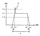
도 9에, 이 라인 빔의 위치에 대한 조사 광 강도 분포를 도시한다. 슬릿(60)에 라인 폭(a)이 규정되고, 대체로 세밀한 경계를 갖는 플랫인 성질로 되어 있지만, 도면의 A 및 B로서 도시한 바와 같은, 강도가 극단적으로 오르거나 낮거나 한 부분이 있고, 플랫인 형상에서 크게 벗어난 부분이 생기고 있다. B는 슬릿(60)의 경계부에서, 파장이 짧은 레이저 광이 회절함으로써 기인하고 있는 것으로 생각된다. 또한, A는 주로 광학계를 구성하는 렌즈(53, 54, 55, 56, 58, 59, 62, 63)에 부착한 이물질 등에 의해 차광, 회절, 간섭 등이 일어나 광강도의 얼룩이 생기고, 이것이 다시 라인 폭 방향으로 집광됨과 동시에, 라인 길이 방향으로 이어져 생긴 것이라고 추측된다. 이와 같이, 광의 얼룩을 생기게 하는 이물질은, 예를 들어 클린룸 내에 조금 존재해도 광학 특성을 영향을 미치고, 강도 분포의 플랫한 성질을 잃는 원인으로 된다.9 shows the irradiation light intensity distribution with respect to the position of this line beam. Although the line width a is defined in the
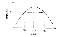
도 10에, a-Si를 ELA에 의해 결정화하여 p-Si로 할 때의 레이저 에너지와 그레인 크기와의 관계를 도시하고 있다. 도면에서, 최적인 에너지(E0)를 정점으로 하여 이보다도 에너지가 작아도 또한 커도 그레인 크기가 작게 되는 것을 알았다. 적어도, 그레인 크기를 r 이상으로 한 경우 에너지는 Ed에서 Eu 사이의 범위내에 있지 않으면 안 된다. 에너지(E0)의 시, 도 9에 있어서 광강도는 I0 또는 에너지(Ed 및 Eu)일 때의 광강도는 각각 Id 및 Iu로 된다. 따라서, A 혹은 B에서 도시되는 바와 같은, 각각 광강도가 Iu보다도 높은 부분 혹은 Id보다도 낮은 부분에서는, 그레인 크기는 충분히 크게 되지 않아 예정의 값(r)이 얻어지지 않는다.Fig. 10 shows the relationship between the laser energy and grain size when a-Si is crystallized by ELA to be p-Si. In the figure, it was found that the optimum energy E0 was taken as the peak and the grain size was reduced even if the energy was smaller than this. At least, when the grain size is greater than r, the energy must be in the range between Ed and Eu. In the case of the energy E 0 , in FIG. 9, the light intensity when I 0 or energy Ed and Eu is Id and Iu, respectively. Therefore, in the portion where the light intensity is higher than Iu or lower than Id, respectively, as shown in A or B, the grain size does not become large enough and the predetermined value r is not obtained.
예를 들어, 도 4에 도시하는 레이저 광 조사 장치에 있어서, 라인 폭이 5∼10mm, 라인 길이가 80∼150mm의 라인 빔이 얻어지고, 이 라인 빔을 피처리 기판(70)상에서, 라인 폭 방향으로의 주사를 복수회 행함으로써 전체에 고르게 레이저 광이 조사되어 대면적을 처리할 수 있지만, 동시에 도 9의 A 혹은 B에 상당하는 영역은, 라인 길이 방향을 따라 선상으로 연장하는 결정화 불량 영역으로 되어 기판(1)상에 다리 모양으로 생기게 된다.For example, in the laser light irradiation apparatus shown in FIG. 4, a line beam having a line width of 5 to 10 mm and a line length of 80 to 150 mm is obtained, and the line beam is line width on the
본 발명은, 이런 문제를 해결하기 위해 구성된 것으로, 기판상에 형성된 다결정 반도체 막의 섬 모양 층과, 상기 다결정 반도체막의 섬 모양 층 중의 채널 영역에 절연막을 통해 중첩 배치된 게이트 전극과, 상기 다결정 반도체막의 섬 모양 층 중의 채널 영역을 사이에 두도록 위치하는 소스 영역 및 드레인 영역에 각각 접속된 소스 전극 및 드레인 전극을 갖고, 상기 다결정 반도체막은 기판상에 형성된 비결정 반도체막에 레이저 빔을 조사함으로써 다결정화하여 얻어지는 반도체 장치의 제조 방법에 있어서, 상기 레이저 빔은 피조사 영역의 에지 라인이 상기 채널 영역의 채널 길이 방향 혹은 채널 폭 방향의 어느 쪽으로도 비직각을 이루도록 조사되는 구성이다.SUMMARY OF THE INVENTION The present invention has been made to solve such a problem, and includes an island-like layer of a polycrystalline semiconductor film formed on a substrate, a gate electrode overlying an insulating layer in a channel region of the island-like layer of the polycrystalline semiconductor film, and the polycrystalline semiconductor film. A source electrode and a drain electrode respectively connected to a source region and a drain region positioned to sandwich a channel region in an island-like layer, wherein the polycrystalline semiconductor film is obtained by polycrystallizing by irradiating a laser beam to an amorphous semiconductor film formed on a substrate; In the manufacturing method of a semiconductor device, the said laser beam is a structure by which the edge line of an irradiated area | region is irradiated so that it may become non-orthogonal in the channel length direction or the channel width direction of the said channel area | region.
이로써, 조사 레이저 빔의 강도의 불균일에 의해, 결정화가 충분히 이루어지지 않는 선형 영역이 전하 이동 경로를 종단하는 일이 없게 되고, 고저항의 개재에 의한 ON 전류의 감소가 방지된다.Thereby, the nonuniformity of the intensity of the irradiated laser beam prevents the linear region in which crystallization is not sufficiently terminated from the charge transfer path, and the reduction of the ON current due to the high resistance intervening is prevented.
상기 레이저 빔은 발진기로부터 조사되는 레이저 광을 복수의 렌즈를 조합시켜 이루어지는 광학계에 의해 피조사 영역을 띠 모양의 라인형으로 정형하여 목적물로 조사하는 라인 빔인 구성이다.The said laser beam is a structure which is a line beam which irradiates a target object by shape | molding a to-be-irradiated area | region in strip shape by the optical system which combines the laser beam irradiated from an oscillator with a some lens.
라인빔의 주사에 의해 실현된 높은 스루풋의 레이저 어닐에 있어서 라인 빔의 강도 분포의 불균일한 부분에 의해 생기는 선형의 결정화 불량 영역이 채널 영역을 종단하는 바와 같이 위치하는 일이 없게 되기 때문에 전하 이동 경로에 고저항이 개재되는 일이 없어, 해당 반도체 소자의 ON 전류가 감소하는 것이 방지된다.In the high throughput laser annealing realized by the scanning of the line beam, the linear crystallization region caused by the uneven portion of the intensity distribution of the line beam is not located as terminating the channel region. The high resistance is not interposed, and the ON current of the semiconductor element is prevented from decreasing.
상기 라인 빔의 라인 길이 방향은, 상기 채널 길이 방향 혹은 채널 폭 방향과 45 °의 각도를 이루는 구성이다.The line length direction of the line beam is configured to form an angle of 45 ° with the channel length direction or the channel width direction.
이로써, 라인 빔 강도의 불균일에 의해 생기는 선형의 결정화 불량 영역이 전하 이동 경로에 대해 항상 45 °의 각도로 위치하게 되어 섬 모양의 다결정 반도체층을 종단하는 일이 없게 되고, 결정화 불량 영역이 전하 이동 경로를 완전하게 분단하여 저항이 증대하고 있던 것이 방지된다.As a result, the linear crystallization defective region caused by the nonuniformity of the line beam intensity is always located at an angle of 45 ° with respect to the charge transfer path, so that the island-shaped polycrystalline semiconductor layer is not terminated, and the crystallization defective region is not transferred. The path is completely divided to prevent the resistance from increasing.
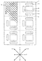
도 1은 본 발명의 실시 형태로, ELA에서의 피처리 기판과, 라인 빔의 조사 및 주사 방향의 관계를 나타내는 평면도이다. 피처리 기판(1)은 보통의 무알칼리 유리 기판이고, 그 표면에는 a-Si가 형성되어 있다. 기판(1)은, 표시 화소가 매트릭스형으로 배치 형성되는 화소부(2)와, 화소부(2) 주변에 배치 형성되는 게이트 드라이버(3) 및 드레인 드라이버(4)로 이루어지는 LCD를 구성하는 액티브 매트릭스 기판(5)을 6매 포함한 마더 글라스 기판이다. 화소부(2)에서는, 액정을 구동하는 화소 캐패시터의 한쪽의 전극인 표시 전극이 매트릭스형으로 배치되고, 이들에 각각 TFT가 접속 형성되게 된다. 게이트 드라이버(3)는 주로 시프트 레지스터로 이루어지고, 드레인 드라이버(4)는 주로 시프트 레지스터 및 샘플 · 홀드 회로로 이루어져 있다. 이들 드라이버는 CMOS 등의 TFT의 어레이에 의해 형성되어 있다.BRIEF DESCRIPTION OF THE DRAWINGS In the embodiment of the present invention, it is a top view which shows the relationship of the to-be-processed board | substrate in ELA, and a line beam irradiation and a scanning direction. The
이 기판(1)에 대해, a-Si를 다결정화하여 p-Si로 하기 위해 ELA가 실시된다. ELA는 도 4에 도시되는 광학계에 의해 실현되는 라인 빔의 조사 및 그 주사이다. 피조사 영역은 그 에지 라인을 파선(C')으로 나타내는 바와 같이 기판의 수직 방향(V) 혹은 수평 방향(H)의 어디에도 45 °의 각도를 이루는 방향(SI) 혹은 이에 직각인 (S2)에 이어지는 띠 형상의 라인 모양이다. 이 라인 빔은 각 조사 펄스를 소정량의 오버랩을 가져 어긋나게 있는 것으로 화살표로 나타내는 방향으로 주사된다.ELA is applied to this
이들 방향(S1, S2)을 따라 라인 빔을 조사했을 때, 도 9에 도시된 광강도가 크게 변화한 부분(A, B)이 통과하여 그레인 사이즈가 충분히 크게 되도록 된 결정화 불량 영역(R')은 기판(1)상의 기울기 45 °의 방향으로 생기게 된다.When the line beams are irradiated along these directions S1 and S2, the regions A 'and B' where the light intensity shown in FIG. 9 greatly changes are passed through so that the grain size becomes large enough. Silver is produced in the direction of inclination 45 ° on the
한편, 기판(1)상에 형성되는 각 TFT는 도 2에 도시되는 바와 같이 섬 모양으로 형성된 p-Si(11)중에 논도핑의 채널 영역(CH), 라이트 도핑된 LD 영역(LD) 및 헤비 도핑된 소스 · 드레인 영역(S, D)이 형성되고, 채널 영역(CH)상에는 게이트 절연막을 끼워 게이트 전극(13)이 배치된다.On the other hand, each TFT formed on the
또한, 도 3은 TFT가 완성되었을 때의 단면도이다. 피처리 기판인 무알칼리 유리의 기판(10)상에 p-Si(11)가 섬 모양으로 형성되고, 논도핑의 채널 영역(CH), 채널 영역(CH)의 양측에 LD 영역(LD), 한편 그 외측에는 소스 및 드레인 영역(S, D)이 형성되어 있다. p-Si(11)상에는, 게이트 절연막(12)이 피복되고, 채널 영역(CH)에 대응하는 영역에는 도핑 p-Si(l3p) 및 텅스텐 실리사이드(13s) 등으로 이루어지는 게이트 전극(13)이 형성되어 있다. 이 게이트 전극(13)상에는, CMOS 구조에서의 다른쪽 도전형의 이온 주입시의 카운터 도핑을 막기 위한 주입 스토퍼(14), 게이트 전극(13) 측벽에는, p-Si(11)에 주입된 불순물이 어닐에 의해 횡방향으로 확산했을 때, 게이트 전극(13)의 경계를 넘어 LD 영역(LD)이 확대되지 않도록 미리 마진을 두기 위한 측벽(15)이 형성되어 있다. 이들을 덮는 전면에는, 제1 층간 절연막(16)이 형성되고, 제1 층간 절연막(16)상에는 저저항 메탈로 이루어지는 드레인 전극(17) 및 소스 전극(18)이 형성되며, 각각 게이트 절연막(12) 및 층간 절연막(16)중에 형성된 콘택트 홀(CT)을 통해 드레인 영역(D) 및 소스 영역(S)에 접속되어 있다. 한편, 이들을 덮는 전면에는, 평탄화 작용이 있는 제2 층간 절연막(19)이 형성되어 있다. 화소부에서는, 제2 층간 절연막(19)상에는, 액정 구동용 표시 전극이 형성되고, 소스 전극(18)상에 개구된 콘택트 홀을 통해 소스 전극(18)에 접속된다. 드레인 및 소스 영역(S, D)과, 드레인 전극(17) 및 소스 전극(18)의 콘택트는 도 2에 있어서 점선으로 둘러싸인 콘택트홀(CT)에서 행하여지고 있다.3 is a cross-sectional view when the TFT is completed. P-Si (11) is formed in an island shape on the
이와 같은 TFT는, 기판(1, 5)에 있어서, 그 채널 길이(L) 방향 혹은 채널 폭(W) 방향이 수직 방향(V) 혹은 평행 방향(H)으로 되도록 형성되어 있다. 따라서, 도 1에 도시하는 바와 같이 라인 빔의 피조사 영역의 에지 라인(C') 방향(S1, S2)을 설정하는 것으로, 도 2에 있어서 피조사 영역의 에지 라인 혹은 이에 라인 길이 방향으로 늘리는 결정화 불량 영역(R')은 TFT의 채널 길이(L) 방향 혹은 채널 폭(W) 방향에 대해서 어느 것도 45 °의 각도를 이루어 위치하게 된다. 이 때문에, 라인 빔의 강도가 크게 변화하여 생기는 결정화 불량 영역(R')은 채널(CH) 및 LCD 영역(LD)을 끼워 소스 · 드레인 영역(S, D)을 연결하는 캐리어 이동 경로를 45 °의 각도를 주어 기울어 통과하게 된다. 이로써, 종래의 도 8에 도시하는 바와 같은 결정화 불량 영역(R)이 캐리어 이동 경로를 완전히 종단하도록 생기는 일이 없게 되고, 도 2에 도시하는 바와 같이 결정화 불량 영역(R')은, TFT의 채널 길이(L) 방향 혹은 채널 폭(W) 방향에 대해서 어느 것도 45 °의 각도로 기울어 위치하게 된다. 이 때문에, 결정화 불량 영역(R')이 채널 영역(CH) 및 LD 영역(LD)을 끼워 소스 · 드레인 영역(S, D) 사이를 연결해 캐리어 이동 경로를 완전하게 분단하는 일이 없게 된다. 예를 들어, 도 8에 있어서, 소스 영역(S) 혹은 LD 영역(LD)에 있어서, 소스 및 드레인(S, D)의 콘택트부(CT) 사이를 완전히 분단하고 있던 결정화 불량 영역(R)은 일부, 도 2에 도시하는 바와 같이 콘택트부(CT)로 침입한다. 이 때문에, 고저항의 결정화 불량 영역(R')을 통과하지 않는 소스 · 드레인 사이 캐리어 이동 경로(CP)가 확보되기 때문에 ON 전류의 감소가 억제된다.Such TFTs are formed in the
특히, 주변 구동 회로에 있어서는, 채널 길이 5∼10㎛에 대해서, 채널 폭이 100∼500㎛로 충분히 크기 때문에, 에지 라인(C)의 방향을, 채널 길이(L ; 채널 폭(W)) 방향에 대해 45 °의 각도로 설정하는 것으로 결정화 불량 영역(R')은 반드시 드레인 및 소스의 콘택트 영역(CT)을 건너게 되기 때문에, 고저항의 결정화 불량 영역(R')을 통과하지 않고 소스 및 드레인(S, D)의 콘택트 홀(CT) 사이를 연결하는 캐리어 이동 경로(CP)가 확보되기 때문에 ON 전류의 감소가 방지된다.In particular, in the peripheral drive circuit, since the channel width is sufficiently large at 100 to 500 µm with respect to the channel length of 5 to 10 µm, the direction of the edge line C is directed to the channel length L (channel width W) direction. By setting it at an angle of 45 ° with respect to the crystallization defective region R ', it is necessary to cross the drain and source contact region CT, so that the source and the crystallization defective region R' do not pass through. Since the carrier movement path CP connecting between the contact holes CT of the drains S and D is secured, the reduction of the ON current is prevented.
이상의 설명으로부터 명확해지는 바와 같이, 본 발명에서 절연성 기판상에 형성된 비정질 반도체층을 레이저 어닐에 의해 재결정화하여 얻어지는 다결정 반도체층을 이용한 반도체 장치의 제조 방법에 있어서, 레이저 광의 피조사 영역의 에지 라인이 피처리 기판의 수직 방향 혹은 수평 방향에 대해 비직각, 특히 45 °로 되도록 함으로써, 에지 라인에 평행하게 생기는 선형의 결정화 불량 영역이 반도체 소자에 이용되는 섬 모양 영역의 채널 길이 혹은 채널 폭 방향에 대해서 기울기 방향을 갖고 위치하게 된다. 이 때문에, 소스 · 드레인 사이를 연결하는 전하 이동 경로중, 결정화 불량 영역을 통과하지 않는 경로가 확보되고, 이 경로가 고저항을 개재하지 않고 소스 · 드레인 사이를 연결하기 때문에 소스 · 드레인 사이에 저항의 증대가 억제되어, 화소부에서의 콘트라스트비의 저하나 주변 구동 회로부에서의 오동작 등의 문제가 방지된다.As is clear from the above description, in the method of manufacturing a semiconductor device using a polycrystalline semiconductor layer obtained by recrystallizing an amorphous semiconductor layer formed on an insulating substrate in the present invention by laser annealing, the edge line of the irradiated region of the laser light is By making it non-perpendicular, in particular 45 °, with respect to the vertical or horizontal direction of the substrate to be processed, the linear crystallization failure region that occurs parallel to the edge line is applied to the channel length or channel width direction of the island-like region used in the semiconductor device. It is positioned with the tilt direction. For this reason, among the charge transfer paths connecting the source and the drain, a path not passing through the poor crystallization region is secured, and this path connects between the source and the drain without intervening a high resistance, thereby providing resistance between the source and the drain. Is suppressed, and problems such as a decrease in contrast ratio in the pixel portion and a malfunction in the peripheral drive circuit portion are prevented.
도 1은 본 발명의 실시 형태에 관한 피처리 기판과 라인 빔의 피조사 영역의 위치 관계를 도시하는 평면도.BRIEF DESCRIPTION OF THE DRAWINGS The top view which shows the positional relationship of the to-be-processed board | substrate which concerns on embodiment of this invention, and the to-be-exposed area | region of a line beam.
도 2는 본 발명에 실시 형태에 관한 TFT 채널 영역과 결정화 불량 영역의 위치 관계를 도시하는 평면도.2 is a plan view showing the positional relationship between a TFT channel region and a poor crystallization region according to the embodiment of the present invention;
도 3은 TFT의 단면도.3 is a cross-sectional view of a TFT.
도 4는 레이저 광 조사 장치의 구성도.4 is a configuration diagram of a laser light irradiation apparatus.
도 5는 레이저 광 조사 장치의 광학계의 구성도.5 is a configuration diagram of an optical system of a laser light irradiation apparatus.
도 6은 레이저 광 조사 장치의 광학계의 구성도.6 is a configuration diagram of an optical system of a laser light irradiation apparatus.
도 7은 종래의 피처리 장치 기판과 라인 빔의 피조사 영역의 위치 관계를 도시하는 평면도.7 is a plan view showing a positional relationship between a conventional substrate to be processed and an irradiated area of a line beam;
도 8은 TFT의 평면도.8 is a plan view of a TFT;
도 9는 조사 레이저 광의 강도 분포도.9 is an intensity distribution diagram of irradiation laser light;
도 10은 레이저 에너지와 그레인 크기의 관계도.10 is a relation between laser energy and grain size.
<도면의 주요 부분에 대한 부호의 설명><Explanation of symbols for the main parts of the drawings>
1 : 피처리 기판1: substrate to be processed
2 : 화소부2: pixel portion
3 : 게이트 드라이버3: gate driver
4 : 드레인 드라이버4: drain driver
5 : 액티브 매트릭스 기판5: active matrix substrate
10 : 기판10: substrate
11 : p-Si11: p-Si
12 : 게이트 절연막12: gate insulating film
13 : 게이트 전극13: gate electrode
17 : 드레인 전극17: drain electrode
18 : 소스 전극18: source electrode
CH : 채널 영역CH: channel area
D : 드레인 영역D: drain region
S : 소스 영역S: source area
CT : 콘택트부CT: Contact
C : 라인 빔의 에지 라인C: edge line of the line beam
R' : 결정화 불량 영역R ': poor crystallization area
Claims (3)
Applications Claiming Priority (2)
| Application Number | Priority Date | Filing Date | Title |
|---|---|---|---|
| JP96-139206 | 1996-05-31 | ||
| JP13920696A JPH09321310A (en) | 1996-05-31 | 1996-05-31 | Manufacture of semiconductor device |
Publications (2)
| Publication Number | Publication Date |
|---|---|
| KR970076045A KR970076045A (en) | 1997-12-10 |
| KR100510001B1 true KR100510001B1 (en) | 2005-11-03 |
Family
ID=15240021
Family Applications (1)
| Application Number | Title | Priority Date | Filing Date |
|---|---|---|---|
| KR1019970022172A KR100510001B1 (en) | 1996-05-31 | 1997-05-30 | Manufacturing method of semiconductor device |
Country Status (5)
| Country | Link |
|---|---|
| US (1) | US6429100B2 (en) |
| EP (1) | EP0810639B1 (en) |
| JP (1) | JPH09321310A (en) |
| KR (1) | KR100510001B1 (en) |
| DE (1) | DE69720856T2 (en) |
Cited By (1)
| Publication number | Priority date | Publication date | Assignee | Title |
|---|---|---|---|---|
| KR100967824B1 (en) * | 2001-11-30 | 2010-07-05 | 가부시키가이샤 한도오따이 에네루기 켄큐쇼 | Manufacturing method for a semiconductor device |
Families Citing this family (69)
| Publication number | Priority date | Publication date | Assignee | Title |
|---|---|---|---|---|
| JP3469337B2 (en) * | 1994-12-16 | 2003-11-25 | 株式会社半導体エネルギー研究所 | Method for manufacturing semiconductor device |
| US6555449B1 (en) | 1996-05-28 | 2003-04-29 | Trustees Of Columbia University In The City Of New York | Methods for producing uniform large-grained and grain boundary location manipulated polycrystalline thin film semiconductors using sequential lateral solidfication |
| TW408246B (en) * | 1997-09-12 | 2000-10-11 | Sanyo Electric Co | Semiconductor device and display device having laser-annealed semiconductor element |
| JPH11214700A (en) * | 1998-01-23 | 1999-08-06 | Semiconductor Energy Lab Co Ltd | Semiconductor display device |
| KR20010071526A (en) | 1998-07-06 | 2001-07-28 | 모리시타 요이찌 | Thin film transistor and liquid crystal display |
| JP2000243968A (en) * | 1999-02-24 | 2000-09-08 | Matsushita Electric Ind Co Ltd | Thin film transistor, manufacture thereof, liquid crystal display device using the same and manufacture thereof |
| JP4663047B2 (en) | 1998-07-13 | 2011-03-30 | 株式会社半導体エネルギー研究所 | Laser irradiation apparatus and method for manufacturing semiconductor device |
| JP4104800B2 (en) * | 1999-12-08 | 2008-06-18 | 三菱電機株式会社 | Liquid crystal display device and TFT panel |
| US6830993B1 (en) | 2000-03-21 | 2004-12-14 | The Trustees Of Columbia University In The City Of New York | Surface planarization of thin silicon films during and after processing by the sequential lateral solidification method |
| MXPA02005590A (en) | 2000-10-10 | 2002-09-30 | Univ Columbia | Method and apparatus for processing thin metal layers. |
| US6573163B2 (en) | 2001-01-29 | 2003-06-03 | Sharp Laboratories Of America, Inc. | Method of optimizing channel characteristics using multiple masks to form laterally crystallized ELA poly-Si films |
| JP2001326365A (en) * | 2001-03-27 | 2001-11-22 | Semiconductor Energy Lab Co Ltd | Semiconductor device |
| SG120880A1 (en) * | 2001-08-31 | 2006-04-26 | Semiconductor Energy Lab | Laser irradiation method, laser irradiation apparatus, and method of manufacturing a semiconductor device |
| US7103576B2 (en) * | 2001-09-21 | 2006-09-05 | First Usa Bank, Na | System for providing cardless payment |
| KR100796758B1 (en) | 2001-11-14 | 2008-01-22 | 삼성전자주식회사 | A mask for crystallizing polysilicon and a method for forming thin film transistor using the mask |
| JP2003179068A (en) * | 2001-12-12 | 2003-06-27 | Hitachi Ltd | Image display device and its manufacturing method |
| EP1326273B1 (en) * | 2001-12-28 | 2012-01-18 | Semiconductor Energy Laboratory Co., Ltd. | Semiconductor device |
| JP4011344B2 (en) * | 2001-12-28 | 2007-11-21 | 株式会社半導体エネルギー研究所 | Method for manufacturing semiconductor device |
| US6933527B2 (en) | 2001-12-28 | 2005-08-23 | Semiconductor Energy Laboratory Co., Ltd. | Semiconductor device and semiconductor device production system |
| JP2003204067A (en) * | 2001-12-28 | 2003-07-18 | Semiconductor Energy Lab Co Ltd | Display device and electronic equipment using the same |
| US6841797B2 (en) | 2002-01-17 | 2005-01-11 | Semiconductor Energy Laboratory Co., Ltd. | Semiconductor device formed over a surface with a drepession portion and a projection portion |
| TWI267131B (en) * | 2002-03-05 | 2006-11-21 | Semiconductor Energy Lab | Semiconductor element and semiconductor device using the same |
| US6847050B2 (en) * | 2002-03-15 | 2005-01-25 | Semiconductor Energy Laboratory Co., Ltd. | Semiconductor element and semiconductor device comprising the same |
| US6930326B2 (en) | 2002-03-26 | 2005-08-16 | Semiconductor Energy Laboratory Co., Ltd. | Semiconductor circuit and method of fabricating the same |
| US6875998B2 (en) * | 2002-03-26 | 2005-04-05 | Semiconductor Energy Laboratory Co., Ltd. | Semiconductor device, method of manufacturing the same, and method of designing the same |
| CN100459041C (en) | 2002-08-19 | 2009-02-04 | 纽约市哥伦比亚大学托管会 | Process and system for laser crystallization processing of film regions on a substrate to minimize edge areas, and structure of such film regions |
| TWI331803B (en) | 2002-08-19 | 2010-10-11 | Univ Columbia | A single-shot semiconductor processing system and method having various irradiation patterns |
| US20040123804A1 (en) | 2002-09-20 | 2004-07-01 | Semiconductor Energy Laboratory Co., Ltd. | Fabrication system and manufacturing method of light emitting device |
| KR100534577B1 (en) * | 2002-11-05 | 2005-12-07 | 삼성에스디아이 주식회사 | Display device having good performance |
| US6906349B2 (en) * | 2003-01-08 | 2005-06-14 | Samsung Electronics Co., Ltd. | Polysilicon thin film transistor array panel and manufacturing method thereof |
| US7387922B2 (en) * | 2003-01-21 | 2008-06-17 | Semiconductor Energy Laboratory Co., Ltd. | Laser irradiation method, method for manufacturing semiconductor device, and laser irradiation system |
| WO2004075263A2 (en) | 2003-02-19 | 2004-09-02 | The Trustees Of Columbia University In The City Of New York | System and process for processing a plurality of semiconductor thin films which are crystallized using sequential lateral solidification techniques |
| KR100956339B1 (en) * | 2003-02-25 | 2010-05-06 | 삼성전자주식회사 | Crystallization system of silicon and crystallization method of silicon |
| FR2852886A1 (en) * | 2003-03-25 | 2004-10-01 | Secap | SECURE PRINT CARTRIDGE |
| US7220627B2 (en) * | 2003-04-21 | 2007-05-22 | Semiconductor Energy Laboratory Co., Ltd. | Method for manufacturing a semiconductor device where the scanning direction changes between regions during crystallization and process |
| US7476629B2 (en) * | 2003-04-21 | 2009-01-13 | Semiconductor Energy Laboratory Co., Ltd. | Beam irradiation apparatus, beam irradiation method, and method for manufacturing thin film transistor |
| US7164152B2 (en) | 2003-09-16 | 2007-01-16 | The Trustees Of Columbia University In The City Of New York | Laser-irradiated thin films having variable thickness |
| US7318866B2 (en) | 2003-09-16 | 2008-01-15 | The Trustees Of Columbia University In The City Of New York | Systems and methods for inducing crystallization of thin films using multiple optical paths |
| WO2005029551A2 (en) | 2003-09-16 | 2005-03-31 | The Trustees Of Columbia University In The City Of New York | Processes and systems for laser crystallization processing of film regions on a substrate utilizing a line-type beam, and structures of such film regions |
| WO2005029546A2 (en) | 2003-09-16 | 2005-03-31 | The Trustees Of Columbia University In The City Of New York | Method and system for providing a continuous motion sequential lateral solidification for reducing or eliminating artifacts, and a mask for facilitating such artifact reduction/elimination |
| WO2005029547A2 (en) | 2003-09-16 | 2005-03-31 | The Trustees Of Columbia University In The City Of New York | Enhancing the width of polycrystalline grains with mask |
| WO2005029549A2 (en) | 2003-09-16 | 2005-03-31 | The Trustees Of Columbia University In The City Of New York | Method and system for facilitating bi-directional growth |
| US7364952B2 (en) * | 2003-09-16 | 2008-04-29 | The Trustees Of Columbia University In The City Of New York | Systems and methods for processing thin films |
| US7311778B2 (en) | 2003-09-19 | 2007-12-25 | The Trustees Of Columbia University In The City Of New York | Single scan irradiation for crystallization of thin films |
| KR100997971B1 (en) | 2003-11-19 | 2010-12-02 | 삼성전자주식회사 | Mask for solidification, method for solidify and method for manufacturing a thin film transistor array panel including the method |
| JP4686122B2 (en) * | 2003-11-28 | 2011-05-18 | 東芝モバイルディスプレイ株式会社 | Active matrix display device and manufacturing method thereof |
| US7812283B2 (en) | 2004-03-26 | 2010-10-12 | Semiconductor Energy Laboratory Co., Ltd. | Laser irradiation method, laser irradiation apparatus, and method for fabricating semiconductor device |
| US8525075B2 (en) | 2004-05-06 | 2013-09-03 | Semiconductor Energy Laboratory Co., Ltd. | Laser irradiation apparatus |
| CN101667538B (en) * | 2004-08-23 | 2012-10-10 | 株式会社半导体能源研究所 | Semiconductor device and its manufacturing method |
| EP1805013A1 (en) * | 2004-10-29 | 2007-07-11 | 3M Innovative Properties Company | Optical films incorporating cyclic olefin copolymers |
| US7645337B2 (en) | 2004-11-18 | 2010-01-12 | The Trustees Of Columbia University In The City Of New York | Systems and methods for creating crystallographic-orientation controlled poly-silicon films |
| US8221544B2 (en) | 2005-04-06 | 2012-07-17 | The Trustees Of Columbia University In The City Of New York | Line scan sequential lateral solidification of thin films |
| JP2009518864A (en) | 2005-12-05 | 2009-05-07 | ザ トラスティーズ オブ コロンビア ユニヴァーシティ イン ザ シティ オブ ニューヨーク | System and method for processing membranes and thin films |
| US7514714B2 (en) * | 2006-02-16 | 2009-04-07 | Stmicroelectronics, Inc. | Thin film power MOS transistor, apparatus, and method |
| US20080135758A1 (en) * | 2006-12-06 | 2008-06-12 | Electronics And Telecommunications Research Institute | Bolometer and method of manufacturing the same |
| US8614471B2 (en) | 2007-09-21 | 2013-12-24 | The Trustees Of Columbia University In The City Of New York | Collections of laterally crystallized semiconductor islands for use in thin film transistors |
| JP5385289B2 (en) | 2007-09-25 | 2014-01-08 | ザ トラスティーズ オブ コロンビア ユニヴァーシティ イン ザ シティ オブ ニューヨーク | Method for producing high uniformity in thin film transistor devices fabricated on laterally crystallized thin films |
| CN103354204A (en) | 2007-11-21 | 2013-10-16 | 纽约市哥伦比亚大学理事会 | Systems and methods for preparation of epitaxially textured thick films |
| WO2009067688A1 (en) | 2007-11-21 | 2009-05-28 | The Trustees Of Columbia University In The City Of New York | Systems and methods for preparing epitaxially textured polycrystalline films |
| US8012861B2 (en) | 2007-11-21 | 2011-09-06 | The Trustees Of Columbia University In The City Of New York | Systems and methods for preparing epitaxially textured polycrystalline films |
| WO2009111340A2 (en) | 2008-02-29 | 2009-09-11 | The Trustees Of Columbia University In The City Of New York | Flash lamp annealing crystallization for large area thin films |
| US8802580B2 (en) | 2008-11-14 | 2014-08-12 | The Trustees Of Columbia University In The City Of New York | Systems and methods for the crystallization of thin films |
| KR20110041107A (en) | 2009-10-15 | 2011-04-21 | 삼성모바일디스플레이주식회사 | Organic light emitting diode display device and fabrication method of the same |
| US9087696B2 (en) | 2009-11-03 | 2015-07-21 | The Trustees Of Columbia University In The City Of New York | Systems and methods for non-periodic pulse partial melt film processing |
| US9646831B2 (en) | 2009-11-03 | 2017-05-09 | The Trustees Of Columbia University In The City Of New York | Advanced excimer laser annealing for thin films |
| US8440581B2 (en) | 2009-11-24 | 2013-05-14 | The Trustees Of Columbia University In The City Of New York | Systems and methods for non-periodic pulse sequential lateral solidification |
| US8575043B2 (en) * | 2011-07-26 | 2013-11-05 | United Microelectronics Corp. | Semiconductor device and manufacturing method thereof |
| JP5907530B2 (en) | 2012-11-20 | 2016-04-26 | 株式会社日本製鋼所 | Laser annealing method and laser annealing apparatus |
| JP7226767B2 (en) * | 2018-11-02 | 2023-02-21 | 株式会社ブイ・テクノロジー | Laser annealing apparatus and laser annealing method |
Citations (3)
| Publication number | Priority date | Publication date | Assignee | Title |
|---|---|---|---|---|
| JPH04712A (en) * | 1990-04-17 | 1992-01-06 | Seiko Epson Corp | Manufacture of thin-film semiconductor crystal layer |
| KR940016602A (en) * | 1992-12-14 | 1994-07-23 | 김광호 | Polycrystalline Crystallization of Amorphous Silicon |
| JPH088179A (en) * | 1994-06-20 | 1996-01-12 | Sharp Corp | Manufacture of semiconductor element |
Family Cites Families (13)
| Publication number | Priority date | Publication date | Assignee | Title |
|---|---|---|---|---|
| US5365875A (en) | 1991-03-25 | 1994-11-22 | Fuji Xerox Co., Ltd. | Semiconductor element manufacturing method |
| TW295703B (en) | 1993-06-25 | 1997-01-11 | Handotai Energy Kenkyusho Kk | |
| JP2814049B2 (en) | 1993-08-27 | 1998-10-22 | 株式会社半導体エネルギー研究所 | Semiconductor device and manufacturing method thereof |
| KR100299292B1 (en) | 1993-11-02 | 2001-12-01 | 이데이 노부유끼 | Polysilicon Thin Film Forming Method and Surface Treatment Apparatus |
| US5496768A (en) | 1993-12-03 | 1996-03-05 | Casio Computer Co., Ltd. | Method of manufacturing polycrystalline silicon thin film |
| US5498904A (en) | 1994-02-22 | 1996-03-12 | Sanyo Electric Co., Ltd. | Polycrystalline semiconductive film, semiconductor device using the same and method of manufacturing the same |
| KR100321541B1 (en) | 1994-03-09 | 2002-06-20 | 야마자끼 순페이 | How Active Matrix Display Devices Work |
| TW280037B (en) | 1994-04-22 | 1996-07-01 | Handotai Energy Kenkyusho Kk | Drive circuit of active matrix type display device and manufacturing method |
| US5712191A (en) * | 1994-09-16 | 1998-01-27 | Semiconductor Energy Laboratory Co., Ltd. | Method for producing semiconductor device |
| JP3919838B2 (en) | 1994-09-16 | 2007-05-30 | 株式会社半導体エネルギー研究所 | Method for manufacturing semiconductor device |
| JP3675886B2 (en) * | 1995-03-17 | 2005-07-27 | 株式会社半導体エネルギー研究所 | Method for manufacturing thin film semiconductor device |
| JP3883592B2 (en) * | 1995-08-07 | 2007-02-21 | 株式会社半導体エネルギー研究所 | Laser irradiation method, semiconductor manufacturing method, semiconductor device manufacturing method, and liquid crystal electro-optical device manufacturing method |
| JPH09260681A (en) | 1996-03-23 | 1997-10-03 | Semiconductor Energy Lab Co Ltd | Manufacture of semiconductor device |
-
1996
- 1996-05-31 JP JP13920696A patent/JPH09321310A/en active Pending
-
1997
- 1997-05-29 US US08/865,476 patent/US6429100B2/en not_active Expired - Lifetime
- 1997-05-30 KR KR1019970022172A patent/KR100510001B1/en not_active IP Right Cessation
- 1997-06-02 EP EP97303681A patent/EP0810639B1/en not_active Expired - Lifetime
- 1997-06-02 DE DE69720856T patent/DE69720856T2/en not_active Expired - Fee Related
Patent Citations (3)
| Publication number | Priority date | Publication date | Assignee | Title |
|---|---|---|---|---|
| JPH04712A (en) * | 1990-04-17 | 1992-01-06 | Seiko Epson Corp | Manufacture of thin-film semiconductor crystal layer |
| KR940016602A (en) * | 1992-12-14 | 1994-07-23 | 김광호 | Polycrystalline Crystallization of Amorphous Silicon |
| JPH088179A (en) * | 1994-06-20 | 1996-01-12 | Sharp Corp | Manufacture of semiconductor element |
Cited By (1)
| Publication number | Priority date | Publication date | Assignee | Title |
|---|---|---|---|---|
| KR100967824B1 (en) * | 2001-11-30 | 2010-07-05 | 가부시키가이샤 한도오따이 에네루기 켄큐쇼 | Manufacturing method for a semiconductor device |
Also Published As
| Publication number | Publication date |
|---|---|
| US6429100B2 (en) | 2002-08-06 |
| DE69720856T2 (en) | 2004-05-06 |
| EP0810639A3 (en) | 1999-07-28 |
| EP0810639B1 (en) | 2003-04-16 |
| US20020001888A1 (en) | 2002-01-03 |
| DE69720856D1 (en) | 2003-05-22 |
| KR970076045A (en) | 1997-12-10 |
| JPH09321310A (en) | 1997-12-12 |
| EP0810639A2 (en) | 1997-12-03 |
Similar Documents
| Publication | Publication Date | Title |
|---|---|---|
| KR100510001B1 (en) | Manufacturing method of semiconductor device | |
| KR100554027B1 (en) | Laser Annealing Method of Semiconductor Film | |
| KR100573657B1 (en) | Display device and semiconductor device having laser annealed semiconductor elements | |
| KR100543102B1 (en) | Semiconductor device and its manufacturing method | |
| KR100560019B1 (en) | Semiconductor device and display device having laser-annealed semiconductor element | |
| KR19990029581A (en) | Semiconductor device and liquid crystal display device | |
| US5477073A (en) | Thin film semiconductor device including a driver and a matrix circuit | |
| KR100374737B1 (en) | METHOD FOR FORMING TRANSISTOR, CIRCUIT CONTAINING THE TRANSISTOR, METHOD FOR PRODUCING ACTIVE MATRIX SUBSTRATE, METHOD FOR MANUFACTURING DISPLAY DEVICE, | |
| US5508216A (en) | Thin film transistor, solid device, display device and manufacturing method of a thin film transistor | |
| KR100250851B1 (en) | Production of polycrystalline silicon thin film transistor | |
| US20040082090A1 (en) | Method for fabricating image display device | |
| JPH09270393A (en) | Laser light irradiation device | |
| US5953598A (en) | Thin film transistor and fabrication process of the same | |
| US6949419B2 (en) | Display device and a method for manufacturing the same | |
| JP3276900B2 (en) | Semiconductor device and display device | |
| JPH10199808A (en) | Method of crystallizing silicon film | |
| JP2002313726A (en) | Laser annealing method for semiconductor film | |
| JPH1187729A (en) | Manufacture of semiconductor device | |
| JP3702232B2 (en) | Laser annealing method for semiconductor film | |
| JP2002313724A (en) | Laser annealing method for semiconductor film | |
| JPH1187670A (en) | Fabrication of semiconductor device |
Legal Events
| Date | Code | Title | Description |
|---|---|---|---|
| A201 | Request for examination | ||
| AMND | Amendment | ||
| E902 | Notification of reason for refusal | ||
| AMND | Amendment | ||
| E601 | Decision to refuse application | ||
| J201 | Request for trial against refusal decision | ||
| AMND | Amendment | ||
| B701 | Decision to grant | ||
| GRNT | Written decision to grant | ||
| FPAY | Annual fee payment |
Payment date: 20120724 Year of fee payment: 8 |
|
| FPAY | Annual fee payment |
Payment date: 20130722 Year of fee payment: 9 |
|
| LAPS | Lapse due to unpaid annual fee |