KR100451291B1 - Faraday cage - Google Patents
Faraday cage Download PDFInfo
- Publication number
- KR100451291B1 KR100451291B1 KR1019970017206A KR19970017206A KR100451291B1 KR 100451291 B1 KR100451291 B1 KR 100451291B1 KR 1019970017206 A KR1019970017206 A KR 1019970017206A KR 19970017206 A KR19970017206 A KR 19970017206A KR 100451291 B1 KR100451291 B1 KR 100451291B1
- Authority
- KR
- South Korea
- Prior art keywords
- substrate
- housing
- conductive
- adhesive
- pwb
- Prior art date
Links
- 239000000853 adhesive Substances 0.000 claims abstract description 45
- 230000001070 adhesive effect Effects 0.000 claims abstract description 45
- 239000000758 substrate Substances 0.000 claims abstract description 33
- 229910052751 metal Inorganic materials 0.000 claims abstract description 17
- 239000002184 metal Substances 0.000 claims abstract description 17
- 239000000463 material Substances 0.000 claims abstract description 11
- 239000004033 plastic Substances 0.000 claims description 4
- 229920003023 plastic Polymers 0.000 claims description 4
- 229920005989 resin Polymers 0.000 claims description 4
- 239000011347 resin Substances 0.000 claims description 4
- 239000003292 glue Substances 0.000 claims 1
- 229920006223 adhesive resin Polymers 0.000 abstract description 5
- 239000004840 adhesive resin Substances 0.000 abstract description 4
- PXHVJJICTQNCMI-UHFFFAOYSA-N Nickel Chemical compound [Ni] PXHVJJICTQNCMI-UHFFFAOYSA-N 0.000 description 14
- 238000000034 method Methods 0.000 description 13
- 229920001343 polytetrafluoroethylene Polymers 0.000 description 13
- 239000004810 polytetrafluoroethylene Substances 0.000 description 13
- -1 polytetrafluoroethylene Polymers 0.000 description 10
- RYGMFSIKBFXOCR-UHFFFAOYSA-N Copper Chemical compound [Cu] RYGMFSIKBFXOCR-UHFFFAOYSA-N 0.000 description 7
- 229910052802 copper Inorganic materials 0.000 description 7
- 239000010949 copper Substances 0.000 description 7
- 239000004744 fabric Substances 0.000 description 7
- 229910052759 nickel Inorganic materials 0.000 description 7
- 229910052782 aluminium Inorganic materials 0.000 description 4
- XAGFODPZIPBFFR-UHFFFAOYSA-N aluminium Chemical compound [Al] XAGFODPZIPBFFR-UHFFFAOYSA-N 0.000 description 4
- ZWEHNKRNPOVVGH-UHFFFAOYSA-N 2-Butanone Chemical group CCC(C)=O ZWEHNKRNPOVVGH-UHFFFAOYSA-N 0.000 description 3
- BQCADISMDOOEFD-UHFFFAOYSA-N Silver Chemical compound [Ag] BQCADISMDOOEFD-UHFFFAOYSA-N 0.000 description 3
- PCHJSUWPFVWCPO-UHFFFAOYSA-N gold Chemical compound [Au] PCHJSUWPFVWCPO-UHFFFAOYSA-N 0.000 description 3
- 229910052737 gold Inorganic materials 0.000 description 3
- 239000010931 gold Substances 0.000 description 3
- 150000002739 metals Chemical class 0.000 description 3
- 229920000728 polyester Polymers 0.000 description 3
- 229910052709 silver Inorganic materials 0.000 description 3
- 239000004332 silver Substances 0.000 description 3
- 229920000106 Liquid crystal polymer Polymers 0.000 description 2
- 239000004977 Liquid-crystal polymers (LCPs) Substances 0.000 description 2
- 239000004952 Polyamide Substances 0.000 description 2
- 239000005062 Polybutadiene Substances 0.000 description 2
- 238000000151 deposition Methods 0.000 description 2
- 238000007772 electroless plating Methods 0.000 description 2
- 230000007613 environmental effect Effects 0.000 description 2
- 239000003822 epoxy resin Substances 0.000 description 2
- 238000004519 manufacturing process Methods 0.000 description 2
- 239000011159 matrix material Substances 0.000 description 2
- 239000012528 membrane Substances 0.000 description 2
- 238000012986 modification Methods 0.000 description 2
- 230000004048 modification Effects 0.000 description 2
- 238000007747 plating Methods 0.000 description 2
- 229920002647 polyamide Polymers 0.000 description 2
- 229920002857 polybutadiene Polymers 0.000 description 2
- 229920001707 polybutylene terephthalate Polymers 0.000 description 2
- 229920000647 polyepoxide Polymers 0.000 description 2
- 229920000139 polyethylene terephthalate Polymers 0.000 description 2
- 239000005020 polyethylene terephthalate Substances 0.000 description 2
- 229920001721 polyimide Polymers 0.000 description 2
- 230000005855 radiation Effects 0.000 description 2
- 229910000679 solder Inorganic materials 0.000 description 2
- 238000001228 spectrum Methods 0.000 description 2
- 229920000178 Acrylic resin Polymers 0.000 description 1
- 239000004925 Acrylic resin Substances 0.000 description 1
- 241000272168 Laridae Species 0.000 description 1
- 239000004698 Polyethylene Substances 0.000 description 1
- 239000004642 Polyimide Substances 0.000 description 1
- 239000004734 Polyphenylene sulfide Substances 0.000 description 1
- 239000004743 Polypropylene Substances 0.000 description 1
- 239000004820 Pressure-sensitive adhesive Substances 0.000 description 1
- 229910000831 Steel Inorganic materials 0.000 description 1
- 125000000218 acetic acid group Chemical group C(C)(=O)* 0.000 description 1
- VOKGLJIUCOOGGW-UHFFFAOYSA-N acetylene;buta-1,3-diene;styrene Chemical compound C#C.C=CC=C.C=CC1=CC=CC=C1 VOKGLJIUCOOGGW-UHFFFAOYSA-N 0.000 description 1
- 238000007744 chromate conversion coating Methods 0.000 description 1
- 239000011248 coating agent Substances 0.000 description 1
- 238000000576 coating method Methods 0.000 description 1
- 239000004020 conductor Substances 0.000 description 1
- 238000007796 conventional method Methods 0.000 description 1
- KAATUXNTWXVJKI-UHFFFAOYSA-N cypermethrin Chemical compound CC1(C)C(C=C(Cl)Cl)C1C(=O)OC(C#N)C1=CC=CC(OC=2C=CC=CC=2)=C1 KAATUXNTWXVJKI-UHFFFAOYSA-N 0.000 description 1
- 230000008021 deposition Effects 0.000 description 1
- 238000005516 engineering process Methods 0.000 description 1
- 150000002148 esters Chemical class 0.000 description 1
- 239000000945 filler Substances 0.000 description 1
- 239000006260 foam Substances 0.000 description 1
- LNEPOXFFQSENCJ-UHFFFAOYSA-N haloperidol Chemical compound C1CC(O)(C=2C=CC(Cl)=CC=2)CCN1CCCC(=O)C1=CC=C(F)C=C1 LNEPOXFFQSENCJ-UHFFFAOYSA-N 0.000 description 1
- 239000007769 metal material Substances 0.000 description 1
- 239000003973 paint Substances 0.000 description 1
- 239000004417 polycarbonate Substances 0.000 description 1
- 229920000515 polycarbonate Polymers 0.000 description 1
- 229920000573 polyethylene Polymers 0.000 description 1
- 239000009719 polyimide resin Substances 0.000 description 1
- 229920000642 polymer Polymers 0.000 description 1
- 229920000069 polyphenylene sulfide Polymers 0.000 description 1
- 229920001155 polypropylene Polymers 0.000 description 1
- 229920002635 polyurethane Polymers 0.000 description 1
- 239000004814 polyurethane Substances 0.000 description 1
- 239000004800 polyvinyl chloride Substances 0.000 description 1
- 229920000915 polyvinyl chloride Polymers 0.000 description 1
- 239000011148 porous material Substances 0.000 description 1
- 239000000843 powder Substances 0.000 description 1
- 238000007650 screen-printing Methods 0.000 description 1
- 229920002050 silicone resin Polymers 0.000 description 1
- 238000005245 sintering Methods 0.000 description 1
- 238000005476 soldering Methods 0.000 description 1
- 239000002904 solvent Substances 0.000 description 1
- 238000004544 sputter deposition Methods 0.000 description 1
- 239000010959 steel Substances 0.000 description 1
- 239000000126 substance Substances 0.000 description 1
- 238000004381 surface treatment Methods 0.000 description 1
- 229920001897 terpolymer Polymers 0.000 description 1
- 229920001169 thermoplastic Polymers 0.000 description 1
- 229920002803 thermoplastic polyurethane Polymers 0.000 description 1
- 229920001187 thermosetting polymer Polymers 0.000 description 1
- 239000004416 thermosoftening plastic Substances 0.000 description 1
Images

Classifications
-
- H—ELECTRICITY
- H05—ELECTRIC TECHNIQUES NOT OTHERWISE PROVIDED FOR
- H05K—PRINTED CIRCUITS; CASINGS OR CONSTRUCTIONAL DETAILS OF ELECTRIC APPARATUS; MANUFACTURE OF ASSEMBLAGES OF ELECTRICAL COMPONENTS
- H05K9/00—Screening of apparatus or components against electric or magnetic fields
- H05K9/0007—Casings
- H05K9/002—Casings with localised screening
- H05K9/0022—Casings with localised screening of components mounted on printed circuit boards [PCB]
- H05K9/0024—Shield cases mounted on a PCB, e.g. cans or caps or conformal shields
- H05K9/0026—Shield cases mounted on a PCB, e.g. cans or caps or conformal shields integrally formed from metal sheet
-
- H—ELECTRICITY
- H05—ELECTRIC TECHNIQUES NOT OTHERWISE PROVIDED FOR
- H05K—PRINTED CIRCUITS; CASINGS OR CONSTRUCTIONAL DETAILS OF ELECTRIC APPARATUS; MANUFACTURE OF ASSEMBLAGES OF ELECTRICAL COMPONENTS
- H05K9/00—Screening of apparatus or components against electric or magnetic fields
-
- H—ELECTRICITY
- H01—ELECTRIC ELEMENTS
- H01L—SEMICONDUCTOR DEVICES NOT COVERED BY CLASS H10
- H01L23/00—Details of semiconductor or other solid state devices
- H01L23/552—Protection against radiation, e.g. light or electromagnetic waves
-
- H—ELECTRICITY
- H05—ELECTRIC TECHNIQUES NOT OTHERWISE PROVIDED FOR
- H05K—PRINTED CIRCUITS; CASINGS OR CONSTRUCTIONAL DETAILS OF ELECTRIC APPARATUS; MANUFACTURE OF ASSEMBLAGES OF ELECTRICAL COMPONENTS
- H05K3/00—Apparatus or processes for manufacturing printed circuits
- H05K3/30—Assembling printed circuits with electric components, e.g. with resistor
- H05K3/32—Assembling printed circuits with electric components, e.g. with resistor electrically connecting electric components or wires to printed circuits
- H05K3/321—Assembling printed circuits with electric components, e.g. with resistor electrically connecting electric components or wires to printed circuits by conductive adhesives
- H05K3/323—Assembling printed circuits with electric components, e.g. with resistor electrically connecting electric components or wires to printed circuits by conductive adhesives by applying an anisotropic conductive adhesive layer over an array of pads
-
- H—ELECTRICITY
- H01—ELECTRIC ELEMENTS
- H01L—SEMICONDUCTOR DEVICES NOT COVERED BY CLASS H10
- H01L2924/00—Indexing scheme for arrangements or methods for connecting or disconnecting semiconductor or solid-state bodies as covered by H01L24/00
- H01L2924/0001—Technical content checked by a classifier
- H01L2924/0002—Not covered by any one of groups H01L24/00, H01L24/00 and H01L2224/00
-
- H—ELECTRICITY
- H01—ELECTRIC ELEMENTS
- H01L—SEMICONDUCTOR DEVICES NOT COVERED BY CLASS H10
- H01L2924/00—Indexing scheme for arrangements or methods for connecting or disconnecting semiconductor or solid-state bodies as covered by H01L24/00
- H01L2924/15—Details of package parts other than the semiconductor or other solid state devices to be connected
- H01L2924/161—Cap
- H01L2924/1615—Shape
- H01L2924/16152—Cap comprising a cavity for hosting the device, e.g. U-shaped cap
-
- H—ELECTRICITY
- H05—ELECTRIC TECHNIQUES NOT OTHERWISE PROVIDED FOR
- H05K—PRINTED CIRCUITS; CASINGS OR CONSTRUCTIONAL DETAILS OF ELECTRIC APPARATUS; MANUFACTURE OF ASSEMBLAGES OF ELECTRICAL COMPONENTS
- H05K2201/00—Indexing scheme relating to printed circuits covered by H05K1/00
- H05K2201/10—Details of components or other objects attached to or integrated in a printed circuit board
- H05K2201/10227—Other objects, e.g. metallic pieces
- H05K2201/10371—Shields or metal cases
Abstract
전기 접지를 갖는 기판과; 그 기판에 전기적으로 접속되는 적어도 하나의 전자 소자와; 전도성 하우징과; 전기 전도성 접착제를 포함하는 EMI/RFI 차폐용 패러데이 케이지가 제공된다. 전기 전도성 접착제는 다수의 관통 통로를 갖는 기판에 의해 형성(define)될 수 있다. 통로는 기판을 형성하는 재료의 복수의 벽에 의해 형성된다. 벽들은 전도성 금속층으로 덮여진다. 통로들은 비전도성 접착제 수지로 채워진다. 전도성 하우징은 전자 소자 전체를 덮도록 기판의 전기 접지에 접착에 의해 전기적으로 장착됨으로써 전자파 장애 및 고주파 잡음 방해를 차폐한다.A substrate having an electrical ground; At least one electronic element electrically connected to the substrate; A conductive housing; A Faraday cage for EMI / RFI shielding comprising an electrically conductive adhesive is provided. The electrically conductive adhesive may be defined by a substrate having a plurality of through passages. The passageway is formed by a plurality of walls of the material forming the substrate. The walls are covered with a conductive metal layer. The passages are filled with a nonconductive adhesive resin. The conductive housing is electrically mounted by bonding to the electrical ground of the substrate to cover the entire electronic device, thereby shielding electromagnetic interference and high frequency noise interference.
Description
전자파 장애(EMI)란 어떤 전기 또는 전자 장치로부터 전도 또는 방사되어 다른 전기 또는 전자 장치의 동작을 방해할 수 있는 원치 않는 전기적 외란(disturbance)으로서 정의되고, 과도적인 것(transient)을 포함한다. 그러한외란은 전자기 스펙트럼내의 어디에서나 발생할 수 있다. 고주파 잡음 방해(RFI)는, 일반적으로 24 킬로헤르쯔(kHz)와 240 기가헤르쯔(GHz)의 사이로서 정의되는 전자파 장애와 호환 가능하게 사용되는 경우가 많지만, 전자기 스펙트럼의 고주파수 부분에 한정되는 것이 더 적절하다.Electromagnetic interference (EMI) is defined as an unwanted electrical disturbance that can interfere with the operation of another electrical or electronic device by conduction or radiation from any electrical or electronic device, including transients. Such disturbances can occur anywhere within the electromagnetic spectrum. High frequency noise interference (RFI) is often used interchangeably with electromagnetic interference, defined generally between 24 kilohertz (kHz) and 240 gigahertz (GHz), but it is more limited to the high frequency portion of the electromagnetic spectrum proper.
차폐는 EMI/RFI의 소스와 보호를 원하는 영역 사이에 삽입된 금속성 또는 다른 전기 전도성 구조로 정의된다. 그러한 차폐는 전자기 에너지가 소스로부터 방사하는 것을 방지하도록 제공될 수 있다. 또한, 그러한 차폐는 차폐된 시스템에 외부의 전자기 에너지가 유입하는 것을 방지할 수도 있다. 실제적으로, 그러한 차폐는 전기적으로 접지된 전기 전도성 하우징의 형태를 취하는 것이 통상적이다. 이에 의해서, EMI/RFI의 에너지가 접지로 무해하게 방산된다.Shielding is defined as a metallic or other electrically conductive structure inserted between the source of EMI / RFI and the desired region of protection. Such shielding may be provided to prevent electromagnetic energy from radiating from the source. Such shielding may also prevent external electromagnetic energy from entering the shielded system. In practice, such shielding is typically in the form of an electrically grounded electrically conductive housing. Thereby, the energy of EMI / RFI is harmlessly dissipated to the ground.
EMI/RFI는 집적 회로(IC) 칩, IC 패키지, 하이브리드 소자 및 멀티-칩 모듈과 같은 전자 소자의 동작을 방해하기 때문에, 다양한 방법들이 전자 소자로부터의 EMI/RFI를 억제하는 데 사용되어 왔다. 가장 일반적인 방법은 전자 소자를 덮는 "캔(can)"을 인쇄 배선 기판과 같은 기판에 전기적으로 접지시키는 것이다. 잘 알려진 바와 같이, 캔은 전도성 하우징, 금속화된 커버, 소형 금속 박스, 주어진 주파수 대역을 초과하는 방사를 최소화시키도록 공간이 배치되어 있는 구멍난 전도성 케이스 형태이거나, 또는 전자 소자를 둘러싸는 다른 형태의 전도성 표면일 수 있다. 캔이 전자 소자를 완전히 둘러싸고 에워싸도록 기판 위에 장착되어 있는 경우, 그것을 흔히 패러데이 케이지라고 칭한다.Various methods have been used to suppress EMI / RFI from electronic devices because EMI / RFI interferes with the operation of electronic devices such as integrated circuit (IC) chips, IC packages, hybrid devices and multi-chip modules. The most common method is to electrically ground a " can " covering the electronic device to a substrate such as a printed wiring board. As is well known, the can can be in the form of a conductive housing, a metallized cover, a small metal box, a hermetically sealed case in which the space is arranged to minimize radiation in excess of a given frequency band, Lt; / RTI > When the can is completely mounted on the substrate so as to surround and enclose the electronic device, it is often called a Faraday cage.
현재, 차폐용으로 전자 소자 주위에 패러데이 케이지를 형성하기 위한 2 가지 주된 방법이 있다. 첫번째 방법은 인쇄 배선 기판(PWB)상의 전자 소자를 둘러싸는 캔을 접지 스트립에 땜납하는 것이다. 그러한 캔을 땜납하면 전기적 특성은 우수하지만, 이 방법은 노동 집약적인 경우가 많다. 또한 땜납된 캔은 전자 소자를 재작업(rework)할 필요가 있을 때 제거하기가 어럽다. 두번째 방법은 예컨대, 복수의 스크류(screw) 또는 클램프(clamp)와 같은 적절한 기계적인 체결 도구(fastener)로 캔 또는 다른 포위체(enclosure)를 기계적으로 고정시키는 것이다. 일반적으로, 전도성 개스킷(gasket) 재료는 캔의 하부 표면에 부착되어, PWB상에서 접지 스트립과 양질의 전기적인 접촉을 보증한다. 캔을 기계적으로 고정시키면 전자 소자의 재작업이 용이하지만, 기계적인 체결 도구는 다루기 힘들고 PWB에서 "귀중한" 공간을 차지한다.Currently, there are two main methods for forming a Faraday cage around an electronic device for shielding. The first method is to solder the can surrounding the electronic component on the printed wiring board (PWB) to the ground strip. Soldering such a can has excellent electrical properties, but this method is often labor intensive. Also, the soldered can is difficult to remove when it is necessary to rework the electronic device. The second method is to mechanically fasten the can or other enclosure to a suitable mechanical fastener, such as, for example, a plurality of screws or clamps. Generally, a conductive gasket material is attached to the bottom surface of the can to ensure good electrical contact with the ground strip on the PWB. Mechanical fastening of the can makes reworking electronic devices easier, but mechanical fastening tools are cumbersome and take up "precious" space in the PWB.
현재까지, 캔을 PWB에 부착시키기 위한 접착제는 현실적으로 고려되지 않아 왔다. 수지 흐름없이 적절한 전기적 특성을 제공하는 전기 전도성 접착제는 존재하지 않는다. 잘 알려진 바와 같이, 전기 소자는 캔에 매우 근접하게 배치되는 경우가 많기 때문에, 전도성 접착제의 흐름으로 인해 전기 소자가 캔에 전기적으로 단락될 수도 있다. 이것은 캔과 완전히 평평하지는 않은 부품을 생산하는 PWB의 제조 공차에 의해 더 어려워진다. 부착되어 있는 부품들의 편차가 캔과 PWB사이에 상당한 갭을 형성할 것이다. 전도성 접착제가 갭이 큰 영역을 채우는 것을 보증하는데 충분한 압력이 가해지면, 전도성 접착제는 갭이 작은 위치로부터 유출될 것이다.Until now, adhesives for attaching cans to PWB have not been considered realistically. There is no electrically conductive adhesive that provides adequate electrical properties without resin flow. As is well known, the electrical element may be electrically short-circuited to the can due to the flow of the conductive adhesive, since the electrical element is often placed very close to the can. This is made more difficult by the manufacturing tolerances of PWBs that produce parts that are not canned and not completely flat. Deviations in the attached components will create a significant gap between the can and the PWB. If sufficient pressure is applied to ensure that the conductive adhesive fills the large area of the gap, the conductive adhesive will flow out of the small gap.
전술한 것은 기존의 패러데이 케이지 설계에 대한 제약을 설명한다. 그러므로, 전술한 하나 이상의 제약을 극복하기 위한 개선된 패러데이 케이지를 제공하는것이 이롭다는 것은 명백하다. 따라서, 이하 더 충분하게 개시되는 특징을 포함하는 적절한 대안이 제공된다.The foregoing describes the constraints on the existing Faraday cage design. It is therefore apparent that it is advantageous to provide an improved Faraday cage for overcoming one or more of the above-mentioned constraints. Accordingly, there is provided a suitable alternative that includes features that are more fully disclosed below.
본 발명은 현재까지 공지되어 있는 것보다 월등하게 전자파 장애 및 고주파 잡음 방해(EMI/RFI) 차폐 기술을 향상시킨 것이다. 본 발명의 일 형태에 의하면, 전기 접지를 갖는 기판과; 상기 기판에 전기적으로 접속되는 적어도 하나의 전자 소자와; 전도성 하우징과; 전기 전도성 접착제를 포함하는 EMI/RFI 차폐용 패러데이 케이지가 제공된다. 상기 전기 전도성 접착제는 다수의 관통 통로를 갖는 기판에 의해 형성(define)될 수 있다. 상기 통로는 상기 기판을 형성하는 재료의 복수의 벽에 의해 형성된다. 상기 벽들은 전도성 금속층으로 덮여진다. 상기 통로들은 비전도성 접착제 수지로 채워진다. 상기 전도성 하우징은 상기 전자 소자 전체를 덮도록 상기 기판의 상기 전기 접지에 접착에 의해 전기적으로 장착됨으로써 전자파 장애 및 고주파 잡음 방해를 차폐한다.The present invention improves electromagnetic interference (EMI) and high frequency noise interference (EMI / RFI) shielding technology far beyond what is known to date. According to an aspect of the present invention, there is provided a plasma display panel comprising: a substrate having an electric ground; At least one electronic element electrically connected to the substrate; A conductive housing; A Faraday cage for EMI / RFI shielding comprising an electrically conductive adhesive is provided. The electrically conductive adhesive may be defined by a substrate having a plurality of through passages. The passageway is defined by a plurality of walls of the material forming the substrate. The walls are covered with a conductive metal layer. The passageways are filled with a nonconductive adhesive resin. The conductive housing is electrically mounted by bonding to the electrical ground of the substrate to cover the entire electronic device, thereby shielding electromagnetic interference and high frequency noise interference.
본 발명의 목적은 신속하고 용이하게 부착되고, 양호한 전기 접지를 제공하고, 소자로의 단락을 조장하지 않으며, 전기 소자를 간단하게 재작업할 수 있는 EMI/RFI 차폐용 패러데이 케이지를 제공하는 것이다.It is an object of the present invention to provide a Faraday cage for EMI / RFI shielding that can be quickly and easily attached, provides good electrical grounding, does not promote short circuit to the device, and can simply rework the electrical device.
도 1은 전자파 장애/고주파 잡음 방해(EMI/RFI)의 차폐를 제공하고, 전도성 접착제에 의해 인쇄 배선 기판(PWB)에 부착된 것으로 도시되어 있는 본 발명의 패러데이 케이지의 단면도.1 is a cross-sectional view of a Faraday cage of the present invention providing shielding of electromagnetic interference / high frequency noise interference (EMI / RFI) and shown attached to a printed wiring board (PWB) by a conductive adhesive;
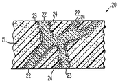
도 2는 본 발명에 따른 적절한 전도성 접착제의 일 실시예의 부분 확대 단면도.2 is a partially enlarged cross-sectional view of one embodiment of a suitable conductive adhesive according to the present invention.
<도면의 주요 부분에 대한 부호의 설명>Description of the Related Art
10 : 패러데이 케이지10: Faraday cage
11 : 전도성 하우징11: Conductive housing
30 : 기판30: substrate
31 : 전기 접지31: Electrical ground
전술한 발명이 이루고자 하는 기술적 과제뿐만 아니라 아래의 본 발명의 바람직한 실시예의 상세한 설명은 첨부된 도면과 관련하여 살펴볼 때 더 잘 이해할 수 있을 것이다. 본 발명을 설명하기 위한 목적으로, 현재의 바람직한 실시예가 도면으로 도시되어 있다. 그러나, 본 발명은 도시되어 있는 바로 그 장치 및 수단으로 제한되지 않는다.BRIEF DESCRIPTION OF THE DRAWINGS The above and other objects, features and advantages of the present invention will be more apparent from the following detailed description taken in conjunction with the accompanying drawings, in which: FIG. For the purpose of illustrating the invention, there is shown in the drawings a presently preferred embodiment. However, the present invention is not limited to the exact apparatus and means shown.
도 1을 통해 가장 잘 볼 수 있듯이, 일반적으로 10으로 표시되는 패러데이 케이지가 EMI/RFI 차폐용으로 제공된다. 패러데이 케이지(10)는 적어도 하나의 전자 소자(40) 전체를 덮도록 기판(30)의 전기 접지(31)에 접착에 의해 전기적으로 장착됨으로써 전자파 장애 및 고주파 잡음 방해를 차폐하는 전도성 하우징(11)을 포함한다.As best seen in Figure 1, a Faraday cage, generally designated 10, is provided for EMI / RFI shielding. The Faraday cage 10 includes a conductive housing 11 that is electrically attached to the
하우징(11)은 예컨대, 0.015 인치 두께의 니켈판과 같은 얇은 금속판으로 형성될 수 있다. 다른 적절한 금속으로는 예컨대, 구리, 알루미늄, 강철 등이 있고, 이것들로 제한되지 않는다. 그것이 알루미늄인 경우에는 크롬산염 전환 코팅으로 표면 처리하거나, 또는 구리 또는 알루미늄인 경우에는 니켈 도금으로 표면 처리하는 것이 바람직할 수 있다. 상기 표면 처리의 양호한 특성은 전기 전도성을 유지하는 동시에 환경 조건에 대한 저항성을 향상시키는 것이다.The housing 11 may be formed of a thin metal plate, for example, a 0.015 inch thick nickel plate. Other suitable metals include, for example, copper, aluminum, steel, and the like, but are not limited thereto. If it is aluminum, it may be surface-treated with a chromate conversion coating, or, in the case of copper or aluminum, it may be preferable to surface-treat it with nickel plating. A good property of the surface treatment is to maintain electrical conductivity while improving resistance to environmental conditions.
하우징(11)에 금속을 사용하는 것 외에도, 필수의 전기적 차폐성을 겸비한 원하는 형상의 하우징을 제공하기 위해서, 플라스틱 재료를 형성하고 금속 처리(metallization)할 수도 있다. 그러한 플라스틱 재료로는 폴리페닐렌 황화물, 폴리아미드, 아세틸, 아세틸렌-부타디엔-스티렌 테르폴리머, 폴리테트라플루오로에틸렌, 폴리비닐 클로라이드, 폴리프로필렌, 폴리에틸렌, 폴리에틸렌 테레프탈레이트(PET), 폴리부틸린 테레프탈레이트(PBT), 폴리카보네이트, 액정 중합체(LCP) 등이 있고, 이것들로 제한되지는 않는다. 상기 표면 금속 처리는 무전해 도금, 증착,스퍼터링, 금속 페인트, 열성형 금속 처리 차폐(thermoformed metallized shielding)등에 의해 제공될 수 있다. 상기 차폐용 금속으로는 구리, 니켈, 은, 금, 알루미늄 등이 있고, 이것들로 제한되지 않는다.In addition to using a metal for the housing 11, a plastic material may be formed and metallized to provide a housing of the desired shape that has the requisite electrical shielding. Examples of such plastic materials include polyphenylene sulfide, polyamide, acetyl, acetylene-butadiene-styrene terpolymer, polytetrafluoroethylene, polyvinyl chloride, polypropylene, polyethylene, polyethylene terephthalate (PET), polybutylene terephthalate (PBT), polycarbonate, liquid crystal polymer (LCP), and the like. The surface metal treatment may be provided by electroless plating, deposition, sputtering, metal paint, thermoformed metallized shielding, and the like. The shielding metal includes, but is not limited to, copper, nickel, silver, gold, and aluminum.
하우징은 임의의 적절한 형상으로 형성될 수 있지만, 일반적으로 하우징은 개방 단부(open end)를 갖는 포위체(encloure)를 형성한다. 개방 단부는 소정의 폭을 갖는 베이스 풋프린트(base footprint)를 형성한다. 하우징의 개방 단부는 전자 소자(40) 전체를 덮도록 배치된다. 하우징(11)은 개개의 전자 소자가 개별적으로 차폐될 수 있도록 분리된 내부 구획들을 형성할 수도 있다.The housing may be formed in any suitable shape, but generally the housing forms an enclosure with an open end. The open end forms a base footprint having a predetermined width. The open end of the housing is disposed so as to cover the entire
도 1에 도시되어 있는 바와 같이, 기판(30)은 인쇄 배선 기판(PWB)을 포함할 수 있다. PWB는 그 위에 장착된 전자 소자들(40)과 전기적으로 접속하여, 적절한 전기적 기능을 수행한다. 전자 소자들은 일련의 전기 접촉 포인트(41)에 의해 PWB에 전기적으로 접속된다. 전자 소자들은 보통은 예컨대, 리드없는(leadless) 패키지, 관통 홀(through hole) 패키지, 갈매기 날개형(gull wing) 패키지, J-리드(J-lead) 패키지, 볼 그리드(ball grid) 어레이, 랜드 그리드(land grid) 어레이, 또는 핀 그리드(pin grid) 어레이 등의 형태이다. 접촉 포인트(41)는 소켓, 땜납, 전도성 접착제, 또는 다른 적절한 수단에 의해 PWB에 부착된다.As shown in FIG. 1, the
도 1에 도시되어 있는 바와 같이, EMI/RFI에 대해 차폐될 필요가 있는 전자 소자(40)는 PWB(30)의 상층의 일부분으로서 형성되는 접지 스트립 또는 링(31)에 의해 둘러싸일 것이다. 이 접지 링은 그 폭이 상기 하우징(11)의 베이스 풋프린트의 폭과 같거나 큰 것이 바람직하다. 접지 링의 전도성 표면은 PWB를 제조하는 데사용되는 임의의 통상적인 방법에 의해 형성될 수 있다. 접지 링(31)을 형성하는 전도성 재료로는 에칭된 구리 또는 스크린 인쇄 중합체 후막이 있고, 이것들로 제한되지 않는다. 전기 전도성을 유지하는 동시에 환경 조건에 대한 저항성을 향상시키기 위해서, 전도성 표면상에 니켈, 금, 은 등과 같은 표면 금속을 도금하는 것이 또한 바람직할 수 있다. 접지 링(31)은 회로선, 도금된 관통 홀 등에 의해 PWB의 전기 회로의 접지 경로에 접속되는 것이 바람직하다.As shown in FIG. 1, the
하우징(11)은 전기 전도성 접착제(20)에 의해 PWB(30)상의 접지 링(31)에 접착에 의해 전기적으로 접속된다. 소자(40)의 임의의 전기 접촉(41)과 접지 링 사이의 간격은 전기 접촉(41)이 하우징(11) 또는 접착제(20) 중 하나에 전기적으로 단락하지 않도록 하기 위한 것이다. 바람직하게는, 적절한 간격은 약 0.040 인치이다.The housing 11 is electrically connected by adhesion to the
본 발명의 바람직한 실시예에서, 전도성 접착제(20)는 기판(21)의 한 쪽에서 다른 쪽으로 연장된 통로(22)가 마련된 기판(21)을 포함한다. 상기 기판은 직물, 다공질 막, 발포체(發泡體) 등일 수 있다. 바람직하게는 접착 기판으로서 사용되었을 때 추종성을 제공하도록 탄력성과 압축성이 있어야 한다. 상기 직물은 그것이 필수적인 통로를 가지고만 있다면, 직물(織物), 부직물(不織物), 편물(編物) 등 어떤 것이어도 좋다. 대표적인 직물로는 폴리아미드, PTFE, 폴리에스테르, 폴리우레탄, 폴리이미드 등이 있다. 강도, 압축성, 온도 저항성 및 화학적 불활성에 대하여 특히 바람직한 기판은 다공성 폴리테트라플루오로에틸렌(PTFE)이다.In a preferred embodiment of the present invention, the
본 명세서에 사용된 용어로서 다공성 폴리테트라플루오로에틸렌(PTFE)은 다수의 공지된 공정들, 예컨대 신장 또는 인장 공정, 제지(papermaking) 공정, 충전제 재료가 PTFE 수지와 혼합된 후 다공성 구조를 남기도록 제거되는 공정, 또는 분말 소결 공정에 의해 제조될 수 있는 막을 의미한다. 바람직하게는, 다공성 폴리테트라플루오로에틸렌 막은 바람직한 재료와 제조 공정을 충분히 기술하고 있고 참조로서 본 명세서에 통합되어 있는 미국 특허 제 3,953,566 호; 제 4,187,390호; 및 제 4,110,392 호에 기술되어 있는 바와 같이, 서로 연결된 노드(node)와 피브릴(fibril)의 미세구조를 갖는 연장된 다공성 폴리테트라플루오로에틸렌 막이다.Porous polytetrafluoroethylene (PTFE) as used herein refers to a porous polytetrafluoroethylene (PTFE) that is formed by a number of known processes such as an elongation or tensile process, a papermaking process, a porous material after the filler material is mixed with the PTFE resin Or a film that can be produced by a powder sintering process. Preferably, the porous polytetrafluoroethylene membrane is described in U.S. Patent Nos. 3,953,566, which fully describes preferred materials and manufacturing processes and is incorporated herein by reference; 4,187,390; And an extended porous polytetrafluoroethylene membrane having a microstructure of fibrils and nodes connected to each other as described in U.S. Patent No. 4,110,392.
기판(21)은 일반적으로 두께 범위가 0.003 인치 내지 약 0.100 인치이고, 일반적으로 박판(sheet)의 형태를 취하지만, 그 형상은 함께 접합되고 있는 소자들에 적합할 수 있다.
통로(22)의 벽에는 무전해 도금 절차에 의해 형성될 수 있는 연속적인 전도성 금속(23)이 부착된다. 대표적인 전도성 금속으로는 구리, 니켈, 은, 금 등이 있다. 상기 금속 코팅 또는 도금은 통로의 체적을 채우지는 않고, 상기 통로를 형성하는 재료를 덮는데 불과하다.Continuous
상기 기판이 폴리에스테르 직물과 같은 중합체 직물인 경우, 그러한 전도성 도금 기판은 상표명 Flectron 재료로 Monsanto Co.로부터 입수될 수 있다.If the substrate is a polymeric fabric such as a polyester fabric, such a conductive plated substrate may be obtained from Monsanto Co. under the trade name Flectron material.
상기 기판이 연장된 다공성 PTFE인 경우, 상기 전도성 도금 기판은 미국 특허 제 4,557,957호에 일반적으로 기술되어 있는 바와 같이 제조될 수 있다.When the substrate is an elongated porous PTFE, the conductive plated substrate may be prepared as generally described in U.S. Patent No. 4,557,957.
일단 상기 전도성 금속 재료가 상기 통로의 벽에 적절히 배치되고 나면, 나머지 통로의 체적은 비전도성 접착제(24)로 채워진다. 적절한 접착제로는 에폭시 수지, 아크릴 수지, 우레탄 수지, 실리콘 수지, 폴리이미드 수지, 시안 에스테르 수지 등이 있다. 상기 접착제는 상기 기판을 그 접착제 용액에 침전시킴으로써 편리하게 상기 통로에 흡수된다. 에폭시 수지 접착제에 적절한 용매는 메틸에틸케톤이다.Once the conductive metal material is properly positioned on the walls of the passageway, the volume of the remaining passageway is filled with the
전도성 하우징(11)은 전도성 하우징(11)과 PWB(30) 사이에 전도성 접착제를 배치하고, 전도성 접착제에 압력 및/또는 열을 가하여, 전도성 접착제를 전도성 하우징의 풋프린트와 접지 링(31)의 표면 양자 모두에 접속시킴으로써, PWB(30)에 부착될 수 있다. 바람직한 접착제는 최소 압력만을 필요로 하고 추가의 열을 필요로 하지 않는 압력에 민감한 접착제 수지를 사용한다. 그러나, 요구되는 성능에 따라, 열가소성, 순간 경화성(snap cure), 또는 열경화성 접착제를 사용하여 전도성 하우징을 PWB에 부착하는 것이 바람직할 수도 있다.The conductive housing 11 is provided with a conductive adhesive between the conductive housing 11 and the
본 발명의 또 다른 실시예에 있어서, 전도성 하우징(11)은 전도성 접착제(20)의 연속된 층과 함께 일체를 이루는 플라스틱 재료에 의해 형성될 수 있다. 이 실시예에서, 전도성 접착제(20)는 필수적인 EMI/RFI 차폐를 제공하기 위한 전도성 하우징에 대한 금속 처리와, 전도성 하우징(11)을 접지 스트립(31)에 접착에 의해 전기적으로 접속시키기 위한 접합 메카니즘으로서의 역할을 한다.In another embodiment of the present invention, the conductive housing 11 may be formed of a plastic material integral with the continuous layer of the
실시예 1Example 1
본 발명의 교시에 따라서, 우선 0.015 인치 두께의 니켈판을 준비하고, 표준 드로우 다운(draw down) 공정을 사용하여 상면, 4개의 측면, 및 개방 하면을 갖는차폐물을 형성함으로써, 전도성 하우징을 마련하여, 패러데이 케이지를 만들었다. 상기 하우징의 하부 에지를 따라, 그 4개의 측면의 에지로부터 0.04 인치 연장한 플랜지형 예지를 형성하였다. 대응하는 PWB상에, 상기 하우징의 풋프린트와 일치하도록 0.05 인치 접지 스트립을 구리로 에칭하였다. 전도성 접착제 링을 레이저 절단하여, 상기 하우징의 풋프린트를 따라 폭이 0.04 인치인 링을 생성하였다. 상기 전도성 접착제는 폴리부타디엔 접착제 수지로 채워진 금속 처리된 연장된 다공성 PTFE 전도성 매트릭스이다. 상기 전도성 접착제는 취급의 편이상 양 면상에 릴리스 라이너(release liner)를 갖는다. 레이저 절단된 전도성 접착제의 한 면으로부터 릴리스 라이너를 제거한 후, 그 접착제 링을 핸드 압력을 사용하여 PWB의 접지 스트립에 부착하였다. 다른 면의 릴리스 라이너를 제거한 후, 상기 하우징을 핸드 압력으로 상기 접착제 위에 배치하였다. 상기 하우징은 상기 하우징의 상부로부터 상기 접지 스트립의 에지까지 4 개의 와이어 마이크로오옴미터로 측정하였을 때 12 mΩ의 전기 저항으로 측정되었다.According to the teachings of the present invention, a conductive housing is first provided by preparing a 0.015 inch thick nickel plate and forming a shield with an upper surface, four sides, and an open surface using a standard drawdown process , And a Faraday cage. Along the lower edge of the housing, a flange-like projection extending 0.04 inches from the edges of the four sides. On the corresponding PWB, 0.05 inch ground strips were etched with copper to match the footprint of the housing. The conductive adhesive ring was laser cut to create a 0.04 inch wide ring along the footprint of the housing. The conductive adhesive is a metal treated extended porous PTFE conductive matrix filled with polybutadiene adhesive resin. The conductive adhesive has a release liner on both sides of the handle. After removing the release liner from one side of the laser cut conductive adhesive, the adhesive ring was attached to the ground strip of the PWB using hand pressure. After removing the release liner on the other side, the housing was placed on the adhesive with hand pressure. The housing was measured with an electrical resistance of 12 milliohms as measured by a four wire micro ohm meter from the top of the housing to the edge of the ground strip.
실시예 2Example 2
본 발명의 교시에 따라, 우선 0.015 인치 두께의 니켈판을 준비하고 표준 드로우 다운(draw down) 공정을 사용하여 상면, 4개의 측면, 및 개방 하면을 갖는 차폐물을 형성함으로써, 하우징을 마련하여, 패러데이 케이지를 만들었다. 상기 하우징의 하부 에지를 따라, 그 4개의 측면의 에지로부터 0.04 인치 연장된 플랜지형 에지를 형성하였다. 대응하는 PWB상에, 상기 하우징의 풋프린트와 일치하도록 0.05 인치 접지 스트립을 구리로 에칭하였다. 전도성 접착제 링을 레이저 절단하여, 상기 하우징의 풋프린트를 따라 폭이 0.04 인치인 링을 생성하였다. 상기 전도성 접착제는 폴리부타디엔 접착제 수지로 채워진 금속 처리된 다공성 폴리에스테르 전도성 매트릭스이다. 상기 전도성 접착제는 취급의 편이상 양 면상에 릴리스 라이너(release liner)를 갖는다. 레이저 절단된 전도성 접착제의 한 면으로부터 릴리스 라이너를 제거한 후, 그 접착제 링을 핸드 압력을 사용하여 PWB의 접지 스트립에 부착하였다. 다른 면의 릴리스 라이너를 제거한 후, 상기 하우징을 핸드 압력으로 상기 접착제 위에 배치하였다. 상기 하우징은 상기 하우징의 상부로부터 상기 접지 스트립의 에지까지 4 개의 와이어 마이크로오옴미터로 측정하였을 때 143 mΩ의 전기 저항으로 측정되었다.In accordance with the teachings of the present invention, a housing is first provided by preparing a 0.015 inch thick nickel plate and forming a shield with a top surface, four sides, and an open bottom using a standard drawdown process, I made a cage. Flanged edges extending 0.04 inches from the edges of the four sides were formed along the lower edge of the housing. On the corresponding PWB, 0.05 inch ground strips were etched with copper to match the footprint of the housing. The conductive adhesive ring was laser cut to create a 0.04 inch wide ring along the footprint of the housing. The conductive adhesive is a metal-treated porous polyester conductive matrix filled with a polybutadiene adhesive resin. The conductive adhesive has a release liner on both sides of the handle. After removing the release liner from one side of the laser cut conductive adhesive, the adhesive ring was attached to the ground strip of the PWB using hand pressure. After removing the release liner on the other side, the housing was placed on the adhesive with hand pressure. The housing was measured with an electrical resistance of 143 mOhms as measured by a four wire micro ohm meter from the top of the housing to the edge of the ground strip.
비록 본 발명의 일부 예시적인 실시예가 상세하게 전술되었지만, 당업자는 본 명세서에 기술되어 있는 신규한 기술적 사상 및 이점으로부터 실질적인 이탈없이 다수의 변형이 가능하다는 것을 용이하게 알 수 있다. 따라서, 그러한 모든 변형은 다음의 청구 범위에 의해 정의되는 바와 같이 본 발명의 범위내에 포함되도록 의도된다.Although some exemplary embodiments of the present invention have been described in detail above, those skilled in the art will readily appreciate that many modifications are possible without departing from the novel spirit and scope of the invention as described herein. Accordingly, all such modifications are intended to be included within the scope of the present invention as defined by the following claims.
본 발명에 의하면, 신속하고 용이하게 부착되고, 양호한 전기 접지를 제공하고, 소자들의 단락을 조장하지 않으며, 전기 소자를 간단하게 재작업할 수 있는 EMI/RFI 차폐용 패러데이 케이지를 제공할 수 있다.According to the present invention, it is possible to provide a Faraday cage for EMI / RFI shielding that can be quickly and easily attached, provides good electrical grounding, does not promote short-circuiting of elements, and can easily rework electric devices.
Claims (4)
Applications Claiming Priority (2)
| Application Number | Priority Date | Filing Date | Title |
|---|---|---|---|
| US08/643,292 | 1996-05-08 | ||
| US08/643,292 US5761053A (en) | 1996-05-08 | 1996-05-08 | Faraday cage |
Publications (2)
| Publication Number | Publication Date |
|---|---|
| KR970078796A KR970078796A (en) | 1997-12-12 |
| KR100451291B1 true KR100451291B1 (en) | 2005-01-13 |
Family
ID=24580167
Family Applications (2)
| Application Number | Title | Priority Date | Filing Date |
|---|---|---|---|
| KR1019970017206A KR100451291B1 (en) | 1996-05-08 | 1997-05-06 | Faraday cage |
| KR1019970017207A KR100455015B1 (en) | 1996-05-08 | 1997-05-06 | A lid assembly for shielding electronic components from emi/rfi interferences |
Family Applications After (1)
| Application Number | Title | Priority Date | Filing Date |
|---|---|---|---|
| KR1019970017207A KR100455015B1 (en) | 1996-05-08 | 1997-05-06 | A lid assembly for shielding electronic components from emi/rfi interferences |
Country Status (6)
| Country | Link |
|---|---|
| US (2) | US5761053A (en) |
| EP (1) | EP0806892B1 (en) |
| JP (1) | JPH1070387A (en) |
| KR (2) | KR100451291B1 (en) |
| DE (1) | DE69700261T2 (en) |
| ES (1) | ES2132997T3 (en) |
Cited By (5)
| Publication number | Priority date | Publication date | Assignee | Title |
|---|---|---|---|---|
| KR100864568B1 (en) * | 2002-02-27 | 2008-10-20 | 후지쯔 가부시끼가이샤 | Metal housing |
| KR20190044295A (en) * | 2017-10-20 | 2019-04-30 | 주식회사 엘지화학 | Method for plasma etching process using faraday box |
| KR20190077810A (en) * | 2017-12-26 | 2019-07-04 | 주식회사 엘지화학 | Method for plasma etching process using faraday box |
| KR20200002161A (en) * | 2018-06-29 | 2020-01-08 | 주식회사 엘지화학 | Method for plasma etching process using faraday box |
| KR20200002162A (en) * | 2018-06-29 | 2020-01-08 | 주식회사 엘지화학 | Method for plasma etching process using faraday box |
Families Citing this family (117)
| Publication number | Priority date | Publication date | Assignee | Title |
|---|---|---|---|---|
| SE511926C2 (en) * | 1997-04-16 | 1999-12-20 | Ericsson Telefon Ab L M | Screen enclosure as well as process for making and using a screen enclosure and mobile phone with screen enclosure |
| SE511330C2 (en) * | 1997-12-29 | 1999-09-13 | Ericsson Telefon Ab L M | Process for producing a circuit board and shielding elements for shielding components on such a circuit board |
| US6613976B1 (en) * | 1998-12-15 | 2003-09-02 | Vanguard Products Corporation | Electromagnetic interference shielding gasket |
| US6673460B2 (en) * | 1999-02-04 | 2004-01-06 | Bridgestone Corporation | Composite structure and production method thereof |
| JP3714088B2 (en) * | 1999-02-18 | 2005-11-09 | 株式会社村田製作所 | Electronic component and manufacturing method thereof |
| JP3287330B2 (en) * | 1999-04-22 | 2002-06-04 | 日本電気株式会社 | High frequency circuit shield structure |
| AU6951500A (en) | 1999-06-07 | 2000-12-28 | Johns Hopkins University, The | Cardiac shock electrode system and corresponding implantable defibrillator system |
| US7596409B2 (en) * | 1999-06-07 | 2009-09-29 | The Johns Hopkins University | Cardiac shock electrode system and corresponding implantable defibrillator system |
| US6399875B1 (en) | 1999-08-13 | 2002-06-04 | Ptmw, Inc. | Lightning protected housing structure |
| US6271465B1 (en) * | 1999-08-31 | 2001-08-07 | Nokia Mobile Phones Limited | Low cost conformal EMI/RFI shield |
| KR100385976B1 (en) * | 1999-12-30 | 2003-06-02 | 삼성전자주식회사 | Circuit board and method for manufacturing thereof |
| JP2001237585A (en) * | 2000-02-22 | 2001-08-31 | Murata Mfg Co Ltd | Electronic component and manufacturing method thereof |
| US6400015B1 (en) * | 2000-03-31 | 2002-06-04 | Intel Corporation | Method of creating shielded structures to protect semiconductor devices |
| DE10026353A1 (en) * | 2000-05-27 | 2001-11-29 | Mannesmann Vdo Ag | Shielded electronic circuit |
| US6757181B1 (en) * | 2000-08-22 | 2004-06-29 | Skyworks Solutions, Inc. | Molded shield structures and method for their fabrication |
| JP4137356B2 (en) * | 2000-09-07 | 2008-08-20 | Tdk株式会社 | Method for manufacturing high-frequency module component including surface acoustic wave element |
| US6515352B1 (en) * | 2000-09-25 | 2003-02-04 | Micron Technology, Inc. | Shielding arrangement to protect a circuit from stray magnetic fields |
| NL1016549C2 (en) | 2000-10-06 | 2002-04-10 | Stork Screens Bv | Method for the production of a card protected against interference radiation with a printed circuit. |
| ATE315888T1 (en) * | 2000-11-20 | 2006-02-15 | Parker Hannifin Corp | INTERFERENCE REDUCTION USING CONDUCTIVE THERMOPLASTIC COMPOSITE MATERIALS |
| US8629005B1 (en) | 2000-11-28 | 2014-01-14 | Knowles Electronics, Llc | Methods of manufacture of bottom port surface mount silicon condenser microphone packages |
| US7434305B2 (en) | 2000-11-28 | 2008-10-14 | Knowles Electronics, Llc. | Method of manufacturing a microphone |
| KR100411206B1 (en) * | 2001-02-19 | 2003-12-18 | 삼성전자주식회사 | Semiconductor package |
| US6844236B2 (en) * | 2001-07-23 | 2005-01-18 | Agere Systems Inc. | Method and structure for DC and RF shielding of integrated circuits |
| US6740959B2 (en) | 2001-08-01 | 2004-05-25 | International Business Machines Corporation | EMI shielding for semiconductor chip carriers |
| US20030130697A1 (en) * | 2001-10-23 | 2003-07-10 | Halperin Henry R. | System and/or method for refibrillation of the heart for treatment of post-countershock pulseless electrical activity and/or asystole |
| US6906396B2 (en) * | 2002-01-15 | 2005-06-14 | Micron Technology, Inc. | Magnetic shield for integrated circuit packaging |
| US7039361B1 (en) * | 2002-02-01 | 2006-05-02 | Ciena Corporation | System and method for reducing electromagnetic interference |
| US7033336B2 (en) * | 2002-03-29 | 2006-04-25 | Gore Enterprise Holdings, Inc. | Proximal catheter assembly having a relief valve |
| JP4024103B2 (en) * | 2002-05-29 | 2007-12-19 | アルプス電気株式会社 | High-frequency circuit connection structure |
| US6952046B2 (en) | 2002-06-19 | 2005-10-04 | Foster-Miller, Inc. | Electronic and optoelectronic component packaging technique |
| JP4195975B2 (en) * | 2002-10-16 | 2008-12-17 | パナソニック株式会社 | High frequency equipment |
| US20040079549A1 (en) * | 2002-10-29 | 2004-04-29 | Yu Yuan Liang | Conductive substrate structure |
| US6816372B2 (en) * | 2003-01-08 | 2004-11-09 | International Business Machines Corporation | System, method and apparatus for noise and heat suppression, and for managing cables in a computer system |
| US7259969B2 (en) * | 2003-02-26 | 2007-08-21 | Wavezero, Inc. | Methods and devices for connecting and grounding an EMI shield to a printed circuit board |
| US6927654B2 (en) * | 2003-02-26 | 2005-08-09 | Raytheon Company | Corrosion resistant waveguide system and method |
| US7248484B2 (en) * | 2003-03-12 | 2007-07-24 | Hewlett-Packard Development Company, L.P. | Electro-magnetic suppressive structure |
| JP4090928B2 (en) * | 2003-03-31 | 2008-05-28 | 信越ポリマー株式会社 | Shield box |
| US7009106B2 (en) * | 2003-10-09 | 2006-03-07 | Bosch Security Systems, Inc. | Shielding assembly and method |
| US7446753B2 (en) * | 2004-09-10 | 2008-11-04 | Hand Held Products, Inc. | Hand held computer device |
| US7446265B2 (en) * | 2005-04-15 | 2008-11-04 | Parker Hannifin Corporation | Board level shielding module |
| US7728417B2 (en) * | 2005-05-27 | 2010-06-01 | Stats Chippac Ltd. | Integrated circuit package system including shield |
| EP1969913A1 (en) * | 2005-12-13 | 2008-09-17 | MALECKI, Zbigniew | System and method for excluding electromagnetic waves from a protected region |
| US7262369B1 (en) | 2006-03-09 | 2007-08-28 | Laird Technologies, Inc. | Combined board level EMI shielding and thermal management |
| US20080080160A1 (en) * | 2005-12-16 | 2008-04-03 | Laird Technologies, Inc. | Emi shielding assemblies |
| US20070163802A1 (en) * | 2006-01-19 | 2007-07-19 | Triquint Semiconductors, Inc. | Electronic package including an electromagnetic shield |
| US7381906B2 (en) * | 2006-03-01 | 2008-06-03 | Sony Ericsson Mobile Communications Ab | Shielding device |
| US7463496B2 (en) * | 2006-03-09 | 2008-12-09 | Laird Technologies, Inc. | Low-profile board level EMI shielding and thermal management apparatus and spring clips for use therewith |
| US7317618B2 (en) * | 2006-03-09 | 2008-01-08 | Laird Technologies, Inc. | Combined board level shielding and thermal management |
| US7623360B2 (en) * | 2006-03-09 | 2009-11-24 | Laird Technologies, Inc. | EMI shielding and thermal management assemblies including frames and covers with multi-position latching |
| CN2891137Y (en) * | 2006-04-10 | 2007-04-18 | 富士康(昆山)电脑接插件有限公司 | Cabled controller |
| KR100782774B1 (en) * | 2006-05-25 | 2007-12-05 | 삼성전기주식회사 | System in package module |
| US7518067B2 (en) * | 2006-09-27 | 2009-04-14 | Advanced Micro Devices, Inc. | Metal cage structure and method for EMI shielding |
| US8063727B2 (en) * | 2006-12-08 | 2011-11-22 | Teradyne, Inc. | Conductive shielding device |
| US20090008431A1 (en) * | 2007-07-03 | 2009-01-08 | Kossi Zonvide | Solderable EMI Gasket and Grounding Pad |
| US20090165815A1 (en) * | 2007-12-03 | 2009-07-02 | United Test And Assembly Center Ltd. | Avoiding electrical shorts in packaging |
| US8167231B2 (en) * | 2007-12-21 | 2012-05-01 | Airbus Deutschland Gmbh | Shielding arrangement for lines, in particular electrical lines, in aircraft |
| US8059416B2 (en) * | 2008-03-31 | 2011-11-15 | Universal Scientific Industrial (Shanghai) Co., Ltd. | Multi-cavity electromagnetic shielding device |
| US8751561B2 (en) * | 2008-04-08 | 2014-06-10 | Roderick B. Wideman | Methods and systems for improved throughput performance in a distributed data de-duplication environment |
| US7759168B2 (en) * | 2008-05-13 | 2010-07-20 | International Business Machines Corporation | Electromagnetic interference shield for semiconductors using a continuous or near-continuous peripheral conducting seal and a conducting lid |
| JP4489133B2 (en) * | 2008-09-10 | 2010-06-23 | 株式会社東芝 | Printed wiring boards, electronic devices |
| US8138864B2 (en) * | 2009-06-01 | 2012-03-20 | Eaton Corporation | Circuit interrupter including a molded case made of liquid crystal polymer |
| US8477499B2 (en) | 2009-06-05 | 2013-07-02 | Laird Technologies, Inc. | Assemblies and methods for dissipating heat from handheld electronic devices |
| US7965514B2 (en) | 2009-06-05 | 2011-06-21 | Laird Technologies, Inc. | Assemblies and methods for dissipating heat from handheld electronic devices |
| JP5625339B2 (en) * | 2009-12-01 | 2014-11-19 | 富士通株式会社 | Shield case and communication device |
| US9030159B2 (en) * | 2010-03-26 | 2015-05-12 | Boston Scientific Neuromodulation Corporation | Inductive charger with magnetic shielding |
| TWI549386B (en) | 2010-04-13 | 2016-09-11 | 康寧吉伯特公司 | Coaxial connector with inhibited ingress and improved grounding |
| US8526161B2 (en) | 2010-04-19 | 2013-09-03 | Apple Inc. | Button structures for electronic devices |
| US20110255250A1 (en) * | 2010-04-19 | 2011-10-20 | Richard Hung Minh Dinh | Printed circuit board components for electronic devices |
| US8610822B2 (en) | 2010-04-19 | 2013-12-17 | Apple Inc. | Camera alignment and mounting structures |
| CA2704683A1 (en) * | 2010-05-28 | 2010-08-12 | Ibm Canada Limited - Ibm Canada Limitee | Grounded lid for micro-electronic assemblies |
| WO2012074775A1 (en) | 2010-11-19 | 2012-06-07 | Analog Devices, Inc. | Packaged integrated device with electrically conductive lid |
| US8654537B2 (en) | 2010-12-01 | 2014-02-18 | Apple Inc. | Printed circuit board with integral radio-frequency shields |
| US8279625B2 (en) | 2010-12-14 | 2012-10-02 | Apple Inc. | Printed circuit board radio-frequency shielding structures |
| KR20120110435A (en) * | 2011-03-29 | 2012-10-10 | 삼성전기주식회사 | Isolation method for radio frequency communication module and radio frequency communication module using the same |
| US9179538B2 (en) | 2011-06-09 | 2015-11-03 | Apple Inc. | Electromagnetic shielding structures for selectively shielding components on a substrate |
| US20130032718A1 (en) * | 2011-08-03 | 2013-02-07 | Robert Bosch Gmbh | Rf immunity improved pyro sensor |
| US20130072057A1 (en) | 2011-09-15 | 2013-03-21 | Donald Andrew Burris | Coaxial cable connector with integral radio frequency interference and grounding shield |
| ITTO20110876A1 (en) * | 2011-09-30 | 2013-03-31 | Stmicroelectronics Malta Ltd | WELDING METHOD OF A HOOD WITH A SUPPORT LAYER |
| WO2013066343A1 (en) | 2011-11-04 | 2013-05-10 | Knowles Electronics, Llc | Embedded dielectric as a barrier in an acoustic device and method of manufacture |
| US9136654B2 (en) | 2012-01-05 | 2015-09-15 | Corning Gilbert, Inc. | Quick mount connector for a coaxial cable |
| CN102779811B (en) | 2012-07-20 | 2015-02-04 | 华为技术有限公司 | Chip package and chip packaging method |
| US9078063B2 (en) | 2012-08-10 | 2015-07-07 | Knowles Electronics, Llc | Microphone assembly with barrier to prevent contaminant infiltration |
| US9287659B2 (en) | 2012-10-16 | 2016-03-15 | Corning Optical Communications Rf Llc | Coaxial cable connector with integral RFI protection |
| US8952503B2 (en) | 2013-01-29 | 2015-02-10 | International Business Machines Corporation | Organic module EMI shielding structures and methods |
| US9172154B2 (en) | 2013-03-15 | 2015-10-27 | Corning Gilbert Inc. | Coaxial cable connector with integral RFI protection |
| US9538693B2 (en) * | 2013-03-15 | 2017-01-03 | A.K. Stamping Company, Inc. | Aluminum EMI / RF shield |
| US10290958B2 (en) | 2013-04-29 | 2019-05-14 | Corning Optical Communications Rf Llc | Coaxial cable connector with integral RFI protection and biasing ring |
| WO2014189718A1 (en) | 2013-05-20 | 2014-11-27 | Corning Optical Communications Rf Llc | Coaxial cable connector with integral rfi protection |
| US9241432B1 (en) | 2013-09-27 | 2016-01-19 | The United States Of America, As Represented By The Secretary Of The Navy | Seawater faraday cage |
| WO2015121875A2 (en) * | 2014-02-17 | 2015-08-20 | Dasari Vamshi Nag | A system and method for improving capabilities of security system integrated with premises |
| CN103943610B (en) | 2014-04-16 | 2016-12-07 | 华为技术有限公司 | A kind of electronic element packaging structure and electronic equipment |
| EP3157214B1 (en) | 2014-06-30 | 2019-11-06 | Huawei Technologies Co., Ltd. | Method, device and system for switching switch modes |
| US9357683B2 (en) * | 2014-09-26 | 2016-05-31 | Laird Technologies, Inc. | Electromagnetic interference (EMI) shielding apparatus including electrically-conductive foam |
| WO2016073309A1 (en) | 2014-11-03 | 2016-05-12 | Corning Optical Communications Rf Llc | Coaxial cable connector with integral rfi protection |
| US9839168B2 (en) * | 2015-01-30 | 2017-12-05 | Digi International Inc. | Systems and methods for serviceable EMI shielding |
| US9584709B2 (en) | 2015-02-17 | 2017-02-28 | Microsoft Technology Licensing, Llc | Actuator housing for shielding electromagnetic interference |
| US10033122B2 (en) | 2015-02-20 | 2018-07-24 | Corning Optical Communications Rf Llc | Cable or conduit connector with jacket retention feature |
| WO2016144039A1 (en) | 2015-03-06 | 2016-09-15 | Samsung Electronics Co., Ltd. | Circuit element package, manufacturing method thereof, and manufacturing apparatus thereof |
| US9794661B2 (en) | 2015-08-07 | 2017-10-17 | Knowles Electronics, Llc | Ingress protection for reducing particle infiltration into acoustic chamber of a MEMS microphone package |
| US10211547B2 (en) | 2015-09-03 | 2019-02-19 | Corning Optical Communications Rf Llc | Coaxial cable connector |
| KR102437673B1 (en) * | 2015-09-09 | 2022-08-26 | 삼성전자주식회사 | Semiconductor device |
| WO2017081527A1 (en) | 2015-11-10 | 2017-05-18 | Smartbox Limited | Systems and methods for assessing a mobile device |
| US9525220B1 (en) | 2015-11-25 | 2016-12-20 | Corning Optical Communications LLC | Coaxial cable connector |
| US10156870B2 (en) * | 2016-01-29 | 2018-12-18 | Google Llc | Flexible electromagnetic interference (EMI) shield |
| US10446309B2 (en) | 2016-04-20 | 2019-10-15 | Vishay Dale Electronics, Llc | Shielded inductor and method of manufacturing |
| US10477737B2 (en) | 2016-05-04 | 2019-11-12 | Samsung Electronics Co., Ltd. | Manufacturing method of a hollow shielding structure for circuit elements |
| US10477687B2 (en) | 2016-08-04 | 2019-11-12 | Samsung Electronics Co., Ltd. | Manufacturing method for EMI shielding structure |
| KR102551657B1 (en) | 2016-12-12 | 2023-07-06 | 삼성전자주식회사 | EMI shielding structure and manufacturing method for the same |
| US10542644B2 (en) | 2016-12-14 | 2020-01-21 | A.K. Stamping Company, Inc. | Two-piece solderable shield |
| JP6817858B2 (en) * | 2017-03-17 | 2021-01-20 | 日本電波工業株式会社 | Surface mount device and its manufacturing method |
| US10594020B2 (en) | 2017-07-19 | 2020-03-17 | Samsung Electronics Co., Ltd. | Electronic device having antenna element and method for manufacturing the same |
| KR102373931B1 (en) | 2017-09-08 | 2022-03-14 | 삼성전자주식회사 | Electromagnetic interference shielding structure |
| US10496137B1 (en) | 2018-09-13 | 2019-12-03 | Fujifilm Sonosite, Inc. | Electronics board mounting system |
| JP6846573B2 (en) * | 2018-11-30 | 2021-03-24 | 積水化学工業株式会社 | Conductive non-woven fabric |
| US11661196B2 (en) * | 2019-06-25 | 2023-05-30 | B/E Aerospace, Inc. | Optimized electronics grounding path for high-frequency noise |
| KR20210105466A (en) * | 2020-02-18 | 2021-08-27 | 삼성전자주식회사 | Memory card Socket and electronic apparatus |
| CN112635436B (en) * | 2020-12-17 | 2023-12-15 | 长江存储科技有限责任公司 | Chip packaging structure and preparation method thereof |
Family Cites Families (27)
| Publication number | Priority date | Publication date | Assignee | Title |
|---|---|---|---|---|
| SE392582B (en) * | 1970-05-21 | 1977-04-04 | Gore & Ass | PROCEDURE FOR THE PREPARATION OF A POROST MATERIAL, BY EXPANDING AND STRETCHING A TETRAFLUORETENE POLYMER PREPARED IN AN PASTE-FORMING EXTENSION PROCEDURE |
| DE2250639B2 (en) * | 1972-10-16 | 1976-03-18 | Siemens AG, 1000 Berlin und 8000 München | ELECTROMAGNETIC SEALING OF CONNECTING JOINTS FOR SCREWED SHIELDING ELEMENTS |
| DE3013991A1 (en) * | 1980-04-11 | 1981-10-15 | Bayer Ag, 5090 Leverkusen | LARGE-SCALE PHOTOVOLTAIC CELL |
| US4575578A (en) * | 1983-01-05 | 1986-03-11 | Keene Corporation | Radiation shielding and thermally conductive gasket with internal bonding agent |
| US4557957A (en) * | 1983-03-18 | 1985-12-10 | W. L. Gore & Associates, Inc. | Microporous metal-plated polytetrafluoroethylene articles and method of manufacture |
| DE3520531A1 (en) * | 1985-06-07 | 1986-12-11 | Hagenuk GmbH, 2300 Kiel | Electromagnetic screening for circuit boards |
| JPS6286841A (en) * | 1985-10-14 | 1987-04-21 | Mitsubishi Electric Corp | High frequency hybrid integrated circuit |
| US4912594A (en) * | 1986-11-03 | 1990-03-27 | The Boeing Company | Integral lightning protection repair system and method for its use |
| US4857668A (en) * | 1988-04-15 | 1989-08-15 | Schlegel Corporation | Multi-function gasket |
| US4967315A (en) * | 1990-01-02 | 1990-10-30 | General Electric Company | Metallized ceramic circuit package |
| US5297007A (en) * | 1990-09-19 | 1994-03-22 | Rockwell International Corporation | E/M shielded RF circuit board |
| JP3003952B2 (en) * | 1991-01-14 | 2000-01-31 | ソニーケミカル株式会社 | Connection structure using anisotropic conductive agent |
| WO1992016095A1 (en) * | 1991-03-04 | 1992-09-17 | Motorola, Inc. | Shielding apparatus for non-conductive electronic circuit package |
| FI109960B (en) * | 1991-09-19 | 2002-10-31 | Nokia Corp | Electronic device |
| US5202536A (en) * | 1992-02-03 | 1993-04-13 | Schlegel Corporation | EMI shielding seal with partial conductive sheath |
| EP0560072A3 (en) * | 1992-03-13 | 1993-10-06 | Nitto Denko Corporation | Anisotropic electrically conductive adhesive film and connection structure using the same |
| US5269810A (en) * | 1992-06-19 | 1993-12-14 | W. L. Gore & Associates, Inc. | Patch electrode |
| KR0135404B1 (en) * | 1992-07-31 | 1998-05-15 | 다케우치 도시아키 | Monolithic crystal oscillator |
| US5318855A (en) * | 1992-08-25 | 1994-06-07 | International Business Machines Corporation | Electronic assembly with flexible film cover for providing electrical and environmental protection |
| US5317107A (en) * | 1992-09-24 | 1994-05-31 | Motorola, Inc. | Shielded stripline configuration semiconductor device and method for making the same |
| DE9214394U1 (en) * | 1992-10-23 | 1992-12-17 | Siemens Ag, 8000 Muenchen, De | |
| JPH06283884A (en) * | 1993-03-25 | 1994-10-07 | Nippon Chemicon Corp | Shielded board and its shield process |
| US5459368A (en) * | 1993-08-06 | 1995-10-17 | Matsushita Electric Industrial Co., Ltd. | Surface acoustic wave device mounted module |
| US5373102A (en) * | 1993-08-19 | 1994-12-13 | The United States Of America As Represented By The Secretary Of The Army | Optically transmissive Faraday cage |
| AU6696494A (en) * | 1993-11-03 | 1995-05-23 | W.L. Gore & Associates, Inc. | Electrically conductive adhesives |
| WO1996006520A1 (en) * | 1994-08-19 | 1996-02-29 | W. L. Gore & Associates, Inc. | A see-through radiation shielded assembly |
| US5566055A (en) * | 1995-03-03 | 1996-10-15 | Parker-Hannifin Corporation | Shieled enclosure for electronics |
-
1996
- 1996-05-08 US US08/643,292 patent/US5761053A/en not_active Expired - Lifetime
- 1996-10-23 US US08/735,838 patent/US5763824A/en not_active Expired - Lifetime
-
1997
- 1997-04-30 DE DE69700261T patent/DE69700261T2/en not_active Expired - Lifetime
- 1997-04-30 EP EP97302949A patent/EP0806892B1/en not_active Expired - Lifetime
- 1997-04-30 ES ES97302949T patent/ES2132997T3/en not_active Expired - Lifetime
- 1997-05-01 JP JP9113969A patent/JPH1070387A/en active Pending
- 1997-05-06 KR KR1019970017206A patent/KR100451291B1/en not_active IP Right Cessation
- 1997-05-06 KR KR1019970017207A patent/KR100455015B1/en not_active IP Right Cessation
Cited By (13)
| Publication number | Priority date | Publication date | Assignee | Title |
|---|---|---|---|---|
| KR100864568B1 (en) * | 2002-02-27 | 2008-10-20 | 후지쯔 가부시끼가이샤 | Metal housing |
| KR20190044295A (en) * | 2017-10-20 | 2019-04-30 | 주식회사 엘지화학 | Method for plasma etching process using faraday box |
| US11276561B2 (en) | 2017-10-20 | 2022-03-15 | Lg Chem, Ltd. | Plasma etching method using Faraday cage |
| KR102273971B1 (en) * | 2017-10-20 | 2021-07-07 | 주식회사 엘지화학 | Method for plasma etching process using faraday box |
| KR102273970B1 (en) * | 2017-12-26 | 2021-07-07 | 주식회사 엘지화학 | Method for plasma etching process using faraday box |
| KR20190077810A (en) * | 2017-12-26 | 2019-07-04 | 주식회사 엘지화학 | Method for plasma etching process using faraday box |
| US11462393B2 (en) | 2017-12-26 | 2022-10-04 | Lg Chem, Ltd. | Plasma etching method using faraday cage |
| JP2021509490A (en) * | 2017-12-26 | 2021-03-25 | エルジー・ケム・リミテッド | Plasma etching method using Faraday cage |
| KR20200002161A (en) * | 2018-06-29 | 2020-01-08 | 주식회사 엘지화학 | Method for plasma etching process using faraday box |
| KR102273084B1 (en) * | 2018-06-29 | 2021-07-06 | 주식회사 엘지화학 | Method for plasma etching process using faraday box |
| US11276563B2 (en) | 2018-06-29 | 2022-03-15 | Lg Chem, Ltd. | Plasma etching method using faraday box |
| KR20200002162A (en) * | 2018-06-29 | 2020-01-08 | 주식회사 엘지화학 | Method for plasma etching process using faraday box |
| KR102548183B1 (en) | 2018-06-29 | 2023-06-28 | 주식회사 엘지화학 | Method for plasma etching process using faraday box |
Also Published As
| Publication number | Publication date |
|---|---|
| US5761053A (en) | 1998-06-02 |
| EP0806892A1 (en) | 1997-11-12 |
| DE69700261T2 (en) | 1999-12-30 |
| KR19980032113A (en) | 1998-07-25 |
| KR100455015B1 (en) | 2005-01-17 |
| EP0806892B1 (en) | 1999-06-09 |
| DE69700261D1 (en) | 1999-07-15 |
| KR970078796A (en) | 1997-12-12 |
| ES2132997T3 (en) | 1999-08-16 |
| JPH1070387A (en) | 1998-03-10 |
| US5763824A (en) | 1998-06-09 |
Similar Documents
| Publication | Publication Date | Title |
|---|---|---|
| KR100451291B1 (en) | Faraday cage | |
| KR100507818B1 (en) | Removable electromagnetic interference shield | |
| US7446265B2 (en) | Board level shielding module | |
| US7161252B2 (en) | Module component | |
| EP0976311B1 (en) | A shielding housing and a method of producing a shielding housing | |
| EP1499172B1 (en) | Electromagnetically shielded circuit device and shielding method therefor | |
| CN1302542C (en) | Module part | |
| US20040240191A1 (en) | Electromagnetic interference shielding for a printed circuit board | |
| EP0806891B1 (en) | A lid assembly for shielding electronic components from EMI/RFI interferences | |
| US10455688B2 (en) | Board level shields with virtual grounding capability | |
| US7609530B2 (en) | Conductive elastomeric shielding device and method of forming same | |
| KR20160018236A (en) | Printed board assembly and manufacturing method thereof | |
| US9332680B2 (en) | Electrical gasket and electronic module having electrical gasket | |
| US6477052B1 (en) | Multiple layer thin flexible circuit board | |
| KR20030076470A (en) | An apparutus and method for EMI and ESD shielding using plastic can in borad of electronic equipment | |
| KR20160143622A (en) | Printed board assembly and manufacturing method thereof | |
| JPS63314898A (en) | Shielding package for surface mounting component | |
| JPH02148894A (en) | Electromagnetic wave shielding structure of electronic equipment | |
| KR20040095039A (en) | Emi shielding apparatus for portable terminal | |
| JP2001044681A (en) | Shield sheet connecting structure |
Legal Events
| Date | Code | Title | Description |
|---|---|---|---|
| A201 | Request for examination | ||
| E701 | Decision to grant or registration of patent right | ||
| GRNT | Written decision to grant | ||
| FPAY | Annual fee payment |
Payment date: 20120906 Year of fee payment: 9 |
|
| FPAY | Annual fee payment |
Payment date: 20130910 Year of fee payment: 10 |
|
| FPAY | Annual fee payment |
Payment date: 20140905 Year of fee payment: 11 |
|
| EXPY | Expiration of term |