KR100280397B1 - 입력버퍼회로 - Google Patents
입력버퍼회로 Download PDFInfo
- Publication number
- KR100280397B1 KR100280397B1 KR1019970039804A KR19970039804A KR100280397B1 KR 100280397 B1 KR100280397 B1 KR 100280397B1 KR 1019970039804 A KR1019970039804 A KR 1019970039804A KR 19970039804 A KR19970039804 A KR 19970039804A KR 100280397 B1 KR100280397 B1 KR 100280397B1
- Authority
- KR
- South Korea
- Prior art keywords
- input buffer
- buffer circuit
- pad
- ground voltage
- input
- Prior art date
- Legal status (The legal status is an assumption and is not a legal conclusion. Google has not performed a legal analysis and makes no representation as to the accuracy of the status listed.)
- Expired - Fee Related
Links
Images





Landscapes
- Logic Circuits (AREA)
Abstract
Description
Claims (1)
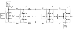
- 전원전압패드 및 전원전압 라인을 통해 전원전압을 소스에 인가 받고, 입력신호에 따라 도통제어되는 피모스 트랜지스터와; 상기 피모스 트랜지스터의 드레인측에 그 드레인이 접속되며, 접지전압패드 및 접지전압 라인을 통해 접지전압을 인가 받고, 게이트에 인가되는 상기 입력신호에 따라 도통제어되는 엔모스 트랜지스터를 각각 구비하는 다수의 입력버퍼회로부를 포함하는 입력버퍼회로에 있어서, 상기 피모스 트랜지스터와 엔모스 트랜지스터는 상기 전원전압 라인 및 접지전압 라인의 고유저항을 고려하여 채널길이 대 채널폭의 비가 각기 다른 것을 사용하는 것을 특징으로 하는 입력버퍼회로.
Priority Applications (1)
| Application Number | Priority Date | Filing Date | Title |
|---|---|---|---|
| KR1019970039804A KR100280397B1 (ko) | 1997-08-21 | 1997-08-21 | 입력버퍼회로 |
Applications Claiming Priority (1)
| Application Number | Priority Date | Filing Date | Title |
|---|---|---|---|
| KR1019970039804A KR100280397B1 (ko) | 1997-08-21 | 1997-08-21 | 입력버퍼회로 |
Publications (2)
| Publication Number | Publication Date |
|---|---|
| KR19990017038A KR19990017038A (ko) | 1999-03-15 |
| KR100280397B1 true KR100280397B1 (ko) | 2001-02-01 |
Family
ID=66047024
Family Applications (1)
| Application Number | Title | Priority Date | Filing Date |
|---|---|---|---|
| KR1019970039804A Expired - Fee Related KR100280397B1 (ko) | 1997-08-21 | 1997-08-21 | 입력버퍼회로 |
Country Status (1)
| Country | Link |
|---|---|
| KR (1) | KR100280397B1 (ko) |
Families Citing this family (1)
| Publication number | Priority date | Publication date | Assignee | Title |
|---|---|---|---|---|
| KR100857438B1 (ko) * | 2007-03-13 | 2008-09-10 | 주식회사 하이닉스반도체 | 전압 생성 회로 및 이를 이용한 반도체 메모리 장치의 기준전압 생성 회로 |
-
1997
- 1997-08-21 KR KR1019970039804A patent/KR100280397B1/ko not_active Expired - Fee Related
Also Published As
| Publication number | Publication date |
|---|---|
| KR19990017038A (ko) | 1999-03-15 |
Similar Documents
| Publication | Publication Date | Title |
|---|---|---|
| EP0717334B1 (en) | Circuit for providing a compensated bias voltage | |
| US6236239B1 (en) | Output buffer circuit achieving stable operation and cost reduction | |
| US6590413B1 (en) | Self-tracking integrated differential termination resistance | |
| KR19990067849A (ko) | 허용 전압 출력 버퍼 | |
| US7863927B2 (en) | Semiconductor device | |
| US6664814B1 (en) | Output driver for an integrated circuit | |
| US5239211A (en) | Output buffer circuit | |
| US6977525B2 (en) | Current driver circuit | |
| US5777496A (en) | Circuit for preventing more than one transistor from conducting | |
| KR100357279B1 (ko) | 풀업회로및반도체장치 | |
| US7609734B2 (en) | Switched gate current driver | |
| US6362655B1 (en) | Linear active resistor and driver circuit incorporating the same | |
| JP2748865B2 (ja) | 出力回路 | |
| JP3146829B2 (ja) | 半導体集積回路 | |
| US7902904B2 (en) | Bias circuit scheme for improved reliability in high voltage supply with low voltage device | |
| KR19990017038A (ko) | 입력버퍼회로 | |
| US5710516A (en) | Input logic signal buffer circuits | |
| EP0150481A2 (en) | High current CMOS output driver circuit | |
| KR100432573B1 (ko) | 임피던스 조절이 가능한 출력 구동 회로를 갖는 반도체 장치 | |
| US9698787B1 (en) | Integrated low voltage differential signaling (LVDS) and high-speed current steering logic (HCSL) circuit and method of use | |
| JP4641660B2 (ja) | レベルシフト回路 | |
| US7893709B2 (en) | Termination circuit | |
| US7084669B2 (en) | Reducing swing line driver | |
| KR100382718B1 (ko) | 출력전류 보상회로를 구비하는 출력드라이버 | |
| JP2646771B2 (ja) | 半導体集積回路 |
Legal Events
| Date | Code | Title | Description |
|---|---|---|---|
| A201 | Request for examination | ||
| PA0109 | Patent application |
St.27 status event code: A-0-1-A10-A12-nap-PA0109 |
|
| PA0201 | Request for examination |
St.27 status event code: A-1-2-D10-D11-exm-PA0201 |
|
| R17-X000 | Change to representative recorded |
St.27 status event code: A-3-3-R10-R17-oth-X000 |
|
| PG1501 | Laying open of application |
St.27 status event code: A-1-1-Q10-Q12-nap-PG1501 |
|
| PN2301 | Change of applicant |
St.27 status event code: A-3-3-R10-R13-asn-PN2301 St.27 status event code: A-3-3-R10-R11-asn-PN2301 |
|
| E902 | Notification of reason for refusal | ||
| PE0902 | Notice of grounds for rejection |
St.27 status event code: A-1-2-D10-D21-exm-PE0902 |
|
| P11-X000 | Amendment of application requested |
St.27 status event code: A-2-2-P10-P11-nap-X000 |
|
| P13-X000 | Application amended |
St.27 status event code: A-2-2-P10-P13-nap-X000 |
|
| E701 | Decision to grant or registration of patent right | ||
| PE0701 | Decision of registration |
St.27 status event code: A-1-2-D10-D22-exm-PE0701 |
|
| GRNT | Written decision to grant | ||
| PR0701 | Registration of establishment |
St.27 status event code: A-2-4-F10-F11-exm-PR0701 |
|
| PR1002 | Payment of registration fee |
St.27 status event code: A-2-2-U10-U11-oth-PR1002 Fee payment year number: 1 |
|
| PG1601 | Publication of registration |
St.27 status event code: A-4-4-Q10-Q13-nap-PG1601 |
|
| PR1001 | Payment of annual fee |
St.27 status event code: A-4-4-U10-U11-oth-PR1001 Fee payment year number: 4 |
|
| PR1001 | Payment of annual fee |
St.27 status event code: A-4-4-U10-U11-oth-PR1001 Fee payment year number: 5 |
|
| PR1001 | Payment of annual fee |
St.27 status event code: A-4-4-U10-U11-oth-PR1001 Fee payment year number: 6 |
|
| PR1001 | Payment of annual fee |
St.27 status event code: A-4-4-U10-U11-oth-PR1001 Fee payment year number: 7 |
|
| PR1001 | Payment of annual fee |
St.27 status event code: A-4-4-U10-U11-oth-PR1001 Fee payment year number: 8 |
|
| FPAY | Annual fee payment |
Payment date: 20081027 Year of fee payment: 9 |
|
| PR1001 | Payment of annual fee |
St.27 status event code: A-4-4-U10-U11-oth-PR1001 Fee payment year number: 9 |
|
| LAPS | Lapse due to unpaid annual fee | ||
| PC1903 | Unpaid annual fee |
St.27 status event code: A-4-4-U10-U13-oth-PC1903 Not in force date: 20091111 Payment event data comment text: Termination Category : DEFAULT_OF_REGISTRATION_FEE |
|
| PC1903 | Unpaid annual fee |
St.27 status event code: N-4-6-H10-H13-oth-PC1903 Ip right cessation event data comment text: Termination Category : DEFAULT_OF_REGISTRATION_FEE Not in force date: 20091111 |
|
| P22-X000 | Classification modified |
St.27 status event code: A-4-4-P10-P22-nap-X000 |