KR100254647B1 - Liquid crystal display device and its drive method and the drive circuit and power supply circuit used therein - Google Patents
Liquid crystal display device and its drive method and the drive circuit and power supply circuit used therein Download PDFInfo
- Publication number
- KR100254647B1 KR100254647B1 KR1019970700243A KR19970700243A KR100254647B1 KR 100254647 B1 KR100254647 B1 KR 100254647B1 KR 1019970700243 A KR1019970700243 A KR 1019970700243A KR 19970700243 A KR19970700243 A KR 19970700243A KR 100254647 B1 KR100254647 B1 KR 100254647B1
- Authority
- KR
- South Korea
- Prior art keywords
- voltage
- group
- voltage level
- liquid crystal
- period
- Prior art date
Links
Images


Classifications
-
- G—PHYSICS
- G09—EDUCATION; CRYPTOGRAPHY; DISPLAY; ADVERTISING; SEALS
- G09G—ARRANGEMENTS OR CIRCUITS FOR CONTROL OF INDICATING DEVICES USING STATIC MEANS TO PRESENT VARIABLE INFORMATION
- G09G3/00—Control arrangements or circuits, of interest only in connection with visual indicators other than cathode-ray tubes
- G09G3/20—Control arrangements or circuits, of interest only in connection with visual indicators other than cathode-ray tubes for presentation of an assembly of a number of characters, e.g. a page, by composing the assembly by combination of individual elements arranged in a matrix no fixed position being assigned to or needed to be assigned to the individual characters or partial characters
- G09G3/34—Control arrangements or circuits, of interest only in connection with visual indicators other than cathode-ray tubes for presentation of an assembly of a number of characters, e.g. a page, by composing the assembly by combination of individual elements arranged in a matrix no fixed position being assigned to or needed to be assigned to the individual characters or partial characters by control of light from an independent source
- G09G3/36—Control arrangements or circuits, of interest only in connection with visual indicators other than cathode-ray tubes for presentation of an assembly of a number of characters, e.g. a page, by composing the assembly by combination of individual elements arranged in a matrix no fixed position being assigned to or needed to be assigned to the individual characters or partial characters by control of light from an independent source using liquid crystals
- G09G3/3611—Control of matrices with row and column drivers
- G09G3/3622—Control of matrices with row and column drivers using a passive matrix
- G09G3/3629—Control of matrices with row and column drivers using a passive matrix using liquid crystals having memory effects, e.g. ferroelectric liquid crystals
-
- G—PHYSICS
- G09—EDUCATION; CRYPTOGRAPHY; DISPLAY; ADVERTISING; SEALS
- G09G—ARRANGEMENTS OR CIRCUITS FOR CONTROL OF INDICATING DEVICES USING STATIC MEANS TO PRESENT VARIABLE INFORMATION
- G09G3/00—Control arrangements or circuits, of interest only in connection with visual indicators other than cathode-ray tubes
- G09G3/20—Control arrangements or circuits, of interest only in connection with visual indicators other than cathode-ray tubes for presentation of an assembly of a number of characters, e.g. a page, by composing the assembly by combination of individual elements arranged in a matrix no fixed position being assigned to or needed to be assigned to the individual characters or partial characters
- G09G3/34—Control arrangements or circuits, of interest only in connection with visual indicators other than cathode-ray tubes for presentation of an assembly of a number of characters, e.g. a page, by composing the assembly by combination of individual elements arranged in a matrix no fixed position being assigned to or needed to be assigned to the individual characters or partial characters by control of light from an independent source
- G09G3/36—Control arrangements or circuits, of interest only in connection with visual indicators other than cathode-ray tubes for presentation of an assembly of a number of characters, e.g. a page, by composing the assembly by combination of individual elements arranged in a matrix no fixed position being assigned to or needed to be assigned to the individual characters or partial characters by control of light from an independent source using liquid crystals
- G09G3/3611—Control of matrices with row and column drivers
- G09G3/3674—Details of drivers for scan electrodes
- G09G3/3681—Details of drivers for scan electrodes suitable for passive matrices only
-
- G—PHYSICS
- G09—EDUCATION; CRYPTOGRAPHY; DISPLAY; ADVERTISING; SEALS
- G09G—ARRANGEMENTS OR CIRCUITS FOR CONTROL OF INDICATING DEVICES USING STATIC MEANS TO PRESENT VARIABLE INFORMATION
- G09G3/00—Control arrangements or circuits, of interest only in connection with visual indicators other than cathode-ray tubes
- G09G3/20—Control arrangements or circuits, of interest only in connection with visual indicators other than cathode-ray tubes for presentation of an assembly of a number of characters, e.g. a page, by composing the assembly by combination of individual elements arranged in a matrix no fixed position being assigned to or needed to be assigned to the individual characters or partial characters
- G09G3/34—Control arrangements or circuits, of interest only in connection with visual indicators other than cathode-ray tubes for presentation of an assembly of a number of characters, e.g. a page, by composing the assembly by combination of individual elements arranged in a matrix no fixed position being assigned to or needed to be assigned to the individual characters or partial characters by control of light from an independent source
- G09G3/36—Control arrangements or circuits, of interest only in connection with visual indicators other than cathode-ray tubes for presentation of an assembly of a number of characters, e.g. a page, by composing the assembly by combination of individual elements arranged in a matrix no fixed position being assigned to or needed to be assigned to the individual characters or partial characters by control of light from an independent source using liquid crystals
- G09G3/3611—Control of matrices with row and column drivers
- G09G3/3685—Details of drivers for data electrodes
- G09G3/3692—Details of drivers for data electrodes suitable for passive matrices only
-
- G—PHYSICS
- G09—EDUCATION; CRYPTOGRAPHY; DISPLAY; ADVERTISING; SEALS
- G09G—ARRANGEMENTS OR CIRCUITS FOR CONTROL OF INDICATING DEVICES USING STATIC MEANS TO PRESENT VARIABLE INFORMATION
- G09G3/00—Control arrangements or circuits, of interest only in connection with visual indicators other than cathode-ray tubes
- G09G3/20—Control arrangements or circuits, of interest only in connection with visual indicators other than cathode-ray tubes for presentation of an assembly of a number of characters, e.g. a page, by composing the assembly by combination of individual elements arranged in a matrix no fixed position being assigned to or needed to be assigned to the individual characters or partial characters
- G09G3/34—Control arrangements or circuits, of interest only in connection with visual indicators other than cathode-ray tubes for presentation of an assembly of a number of characters, e.g. a page, by composing the assembly by combination of individual elements arranged in a matrix no fixed position being assigned to or needed to be assigned to the individual characters or partial characters by control of light from an independent source
- G09G3/36—Control arrangements or circuits, of interest only in connection with visual indicators other than cathode-ray tubes for presentation of an assembly of a number of characters, e.g. a page, by composing the assembly by combination of individual elements arranged in a matrix no fixed position being assigned to or needed to be assigned to the individual characters or partial characters by control of light from an independent source using liquid crystals
- G09G3/3611—Control of matrices with row and column drivers
- G09G3/3696—Generation of voltages supplied to electrode drivers
-
- G—PHYSICS
- G09—EDUCATION; CRYPTOGRAPHY; DISPLAY; ADVERTISING; SEALS
- G09G—ARRANGEMENTS OR CIRCUITS FOR CONTROL OF INDICATING DEVICES USING STATIC MEANS TO PRESENT VARIABLE INFORMATION
- G09G2300/00—Aspects of the constitution of display devices
- G09G2300/04—Structural and physical details of display devices
- G09G2300/0469—Details of the physics of pixel operation
- G09G2300/0478—Details of the physics of pixel operation related to liquid crystal pixels
- G09G2300/0482—Use of memory effects in nematic liquid crystals
- G09G2300/0486—Cholesteric liquid crystals, including chiral-nematic liquid crystals, with transitions between focal conic, planar, and homeotropic states
-
- G—PHYSICS
- G09—EDUCATION; CRYPTOGRAPHY; DISPLAY; ADVERTISING; SEALS
- G09G—ARRANGEMENTS OR CIRCUITS FOR CONTROL OF INDICATING DEVICES USING STATIC MEANS TO PRESENT VARIABLE INFORMATION
- G09G2310/00—Command of the display device
- G09G2310/06—Details of flat display driving waveforms
-
- G—PHYSICS
- G09—EDUCATION; CRYPTOGRAPHY; DISPLAY; ADVERTISING; SEALS
- G09G—ARRANGEMENTS OR CIRCUITS FOR CONTROL OF INDICATING DEVICES USING STATIC MEANS TO PRESENT VARIABLE INFORMATION
- G09G2310/00—Command of the display device
- G09G2310/06—Details of flat display driving waveforms
- G09G2310/061—Details of flat display driving waveforms for resetting or blanking
-
- G—PHYSICS
- G09—EDUCATION; CRYPTOGRAPHY; DISPLAY; ADVERTISING; SEALS
- G09G—ARRANGEMENTS OR CIRCUITS FOR CONTROL OF INDICATING DEVICES USING STATIC MEANS TO PRESENT VARIABLE INFORMATION
- G09G2330/00—Aspects of power supply; Aspects of display protection and defect management
- G09G2330/02—Details of power systems and of start or stop of display operation
-
- G—PHYSICS
- G09—EDUCATION; CRYPTOGRAPHY; DISPLAY; ADVERTISING; SEALS
- G09G—ARRANGEMENTS OR CIRCUITS FOR CONTROL OF INDICATING DEVICES USING STATIC MEANS TO PRESENT VARIABLE INFORMATION
- G09G3/00—Control arrangements or circuits, of interest only in connection with visual indicators other than cathode-ray tubes
- G09G3/20—Control arrangements or circuits, of interest only in connection with visual indicators other than cathode-ray tubes for presentation of an assembly of a number of characters, e.g. a page, by composing the assembly by combination of individual elements arranged in a matrix no fixed position being assigned to or needed to be assigned to the individual characters or partial characters
- G09G3/34—Control arrangements or circuits, of interest only in connection with visual indicators other than cathode-ray tubes for presentation of an assembly of a number of characters, e.g. a page, by composing the assembly by combination of individual elements arranged in a matrix no fixed position being assigned to or needed to be assigned to the individual characters or partial characters by control of light from an independent source
- G09G3/36—Control arrangements or circuits, of interest only in connection with visual indicators other than cathode-ray tubes for presentation of an assembly of a number of characters, e.g. a page, by composing the assembly by combination of individual elements arranged in a matrix no fixed position being assigned to or needed to be assigned to the individual characters or partial characters by control of light from an independent source using liquid crystals
- G09G3/3611—Control of matrices with row and column drivers
- G09G3/3614—Control of polarity reversal in general
Abstract
1프레임중에 적어도 리셋기간 선택기간 및 비선택기간을 가지는 주사신호와 데이터 신호의 차전압을 적어도 2개의 안정상태를 갖는 키랄 네마틱 액정에 인가하는 액정표시장치 및 그 구동 방법이다. 저전압측의 제 1군의 복수레벨(V1, V2, V3, V4)과 고전압측의 제 2군의 복수레벨(V5, V6, V7, V8)로 된 총 8레벨의 전압레벨을 준비한다. 주사신호 Yi의 선택기간 T2에 상당하는 단위시간(1H)의 정수배 mH(m은 2이상의 정수이며 mH≠1프레임기간)마다 주사신호 Yi 및 데이터 신호 Xj의 전압레벨을 각각 제 1군, 제 2군 사이에서 번갈아 변경한다. 데이터 신호(Xj)가 제 1군 전압레벨인 때는 주사신호(Yi)중 리셋기간(T1)의 전압레벨을 제 2군중에서 선택하며 데이터 신호(Xj)가 제 2군 전압레벨인 때는 주사신호(Yi)중 리셋기간(T1)의 전압레벨을 제 1군중에서 선택한다. 데이터 신호(Xj)가 제 1군 전압레벨인 때는 주사신호(Yi)중 선택기간(T3) 및 비선택기간(T4)의 전압레벨을 같은 제 1군중에서 각각 선택하며 데이터 신호가 제 2군 전압레벨인 때는 주사신호(Yi)중 선택기간(T3) 및 비선택기간(T4)의 전압레벨을 같은 제 2군중에서 각각 선택한다. 이에따라 액정에 인가하는 전압 극성이 mH 마다에 반전한다.A liquid crystal display device and a driving method for applying a difference voltage between a scan signal and a data signal having at least a reset period selection period and a non-selection period in one frame to a chiral nematic liquid crystal having at least two stable states. A total of eight levels of voltage levels consisting of the plurality of levels V1, V2, V3, V4 on the low voltage side and the plurality of levels V5, V6, V7, V8 on the second group on the high voltage side are prepared. The first and second voltage levels of the scan signal Yi and the data signal Xj are respectively set for each integer time mH (m is an integer of 2 or more and mH ≠ 1 frame period) corresponding to the selection period T2 of the scan signal Yi. Alternate between armies. When the data signal Xj is at the first group voltage level, the voltage level of the reset period T1 among the scan signals Yi is selected from the second group. When the data signal Xj is at the second group voltage level, the scan signal ( The voltage level of the reset period T1 during Yi) is selected from the first group. When the data signal Xj is at the first group voltage level, the voltage levels of the selection period T3 and the non-selection period T4 among the scanning signals Yi are respectively selected from the same first group, and the data signal is the second group voltage. In the case of the level, the voltage levels of the selection period T3 and the non-selection period T4 of the scanning signal Yi are respectively selected from the same second group. As a result, the voltage polarity applied to the liquid crystal is inverted every mH.
Description
[발명의 명칭][Name of invention]
액정 표시 장치와 그 구동 방법 및 이에 이용되는 구동 회로 및 전원 회로 장치Liquid crystal display, its driving method, driving circuit and power circuit device used therein
[기술분야][Technical Field]
본 발명은 키랄 네마틱 액정을 사용한 메모리성을 갖는 쌍안정의 액정 표시 장치, 그 구동 방법 및 그것에 사용하는 구동 회로에 관한 것으로 특히, 키랄 네마틱 액정 구동에 가장 적합한 총 8 레벨 이상의 전압 레벨을 설정하는 액정 표시 장치 및 이에 사용되는 전원 회로 장치에 관한 것이다.The present invention relates to a bistable liquid crystal display device having a memory property using a chiral nematic liquid crystal, a driving method thereof, and a driving circuit used therein. In particular, a total voltage level of 8 or more levels most suitable for chiral nematic liquid crystal driving is set. The present invention relates to a liquid crystal display device and a power supply circuit device used therein.
[배경기술][Background]
키랄 네마틱 액정을 사용한 쌍안정성 액정 표시는 특공평 1-51818 에 이미 개시되어 있으며 초기 배향조건, 2개의 안정 상태, 또는 그 안정 상태의 실현 방법등이 기재되어 있다.Bistable liquid crystal displays using chiral nematic liquid crystals are already disclosed in Japanese Patent Application Laid-Open No. 1-51818, and describe an initial alignment condition, two stable states, or a method of realizing the stable state.
그러나, 상기 일본특허공개공보 평1-51818호에 기재되어 있는 내용은 2개의 안정 상태의 동작 또는 현상을 기술하고 있을 뿐 그것을 표시체로서 실용에 이용되는 수단은 제시되어 있지 않다. 더욱이, 상기 공보에는 현재, 표시체로서 응용 실용성이 가장 높고 또한 표시 능력이 높은 매트릭스 표시에 대해 아무런 기술이 없고 그 구동 방법에 관하여도 전혀 개시되어 있지 않다.However, the contents described in Japanese Unexamined Patent Publication No. Hei 1-51818 describe two stable states of operation or phenomena, and no means for practical use thereof as a display is disclosed. Moreover, the above publication currently has no description of the matrix display having the highest application practicality and high display capability as a display body, and no driving method is disclosed at all.
그래서, 우리들은 먼저 출원한 특개평 제6-230751호에서 액정 셀중에 발생하는 백플로를 컨트롤하여 상기 결점을 개량하는 방법을 제안했다. 이 방법은 먼저 1ms 정도의 고전압을 인가하여 플레델리코스 전이를 생기게 하는 기간과, 그것에 바로 이어지는 상기 펄스와 역극성 또는 동극성의 문턱전압 이상의 정전압 펄스로 0°의 일정한 상태를 만들거나 마찬가지로 상기 플레델리코스 전이 전압에 바로 이어지는 문턱전압 이하의 펄스 기간을 설정하고 360° 트위스트 상태를 실현하는 것이다. 이 방법에서는 매트릭스 표시의 1 라인당의 기입 시간이 400㎲ 로 되어 있고, 400 라인 이상의 기입에는 총 160ms(6.25Hz) 이상의 시간이 필요하고, 이것은 표시 플리거를 수반하기 때문에 실용상 문제가 있었다.Therefore, we proposed a method of controlling the backflow occurring in the liquid crystal cell in the previously disclosed Japanese Patent Application Laid-Open No. Hei 6-230751 to improve the above-mentioned drawback. This method first creates a constant state of 0 ° with a period of time that a high voltage of about 1 ms is applied to cause a pledelicos transition, and the pulse immediately following it and a constant voltage pulse above a threshold voltage of reverse polarity or unipolarity or similarly. It is to set the pulse period below the threshold voltage immediately following the coarse transition voltage and realize the 360 ° twisted state. In this method, the writing time per line of the matrix display is 400 ms, and writing over 400 lines requires a total time of 160 ms (6.25 Hz) or more, and this has a problem in practical use because it involves display flicker.
그래서 본 발명자들은 또다른 기입 시간의 개량 수단으로서 특원평 5-37057을 출원했다. 이는 동출원의 도 2 또는 도 4 에 보인 바와 같이 플레델리코스 전이를 일으키는 리셋 펄스 후에 지연시간을 설정하고 그후에 온 또는 오프의 선택신호를 인가하는 것이다. 이렇게 하면 기입 시간은 종래의 수배 속도, 예컨대 50㎲ 가 실현가능하다.Therefore, the present inventors have filed Japanese Patent Application No. 5-37057 as a means for improving another writing time. This is to set the delay time after the reset pulse causing the pdelidelicos transition as shown in Fig. 2 or 4 of the same application and then apply the on or off selection signal. In this way, the write time can be realized with a conventional arrangement speed, for example, 50 ms.
그러나, 이들 구동방법으로는 20V를 초과하는 큰 리셋 전압과 2개의 표시 안정 상태를 얻는 오프 전압(1~3V)과 온 전압(수 V)에서 6.7V 정도의 선택 전압을 회로 상에서 효율 좋게 양립시키고 또한 액정의 장수명화를 위한 교류화도 도모하지 않으면 안되다.However, in these driving methods, a large reset voltage exceeding 20 V, an off voltage (1 to 3 V) obtaining two display stable states, and a selection voltage of about 6.7 V at the on voltage (a few V) can be efficiently achieved in the circuit. In addition, the exchange for the long life of the liquid crystal must be promoted.
도 23 은 전압 평균화법을 답습하여, 쌍안정표시의 구동파형을 만든 7 레벨 구동법을 나타내었다. 도 23(a)는 주사 신호의 파형이며 리셋 기간T1 에는 20V 를 초과하는 Vr 를 가하고 지연기간 T2 후에 오는 지연시간 T3 에는 ±Vs, 나머지 비선택기간 T4 는 제로 전위로 한다. 한편 데이터 신호는 동도(b)에 나타낸 진폭 ±Vd 의 선택 펄스에 동상 또는 역상의 교류 펄스를 가하여 표시 온/오프를 행한다. 그리하여 도 23(c)에 보인바와 같은 주사 신호와 데이터 신호의 차신호 전압이 액정에 인가하게 된다.Fig. 23 shows a seven-level driving method in which a drive waveform of bistable display is made by following the voltage averaging method. Fig. 23A is a waveform of the scan signal, and Vr exceeding 20V is applied to the reset period T1, ± Vs is added to the delay time T3 following the delay period T2, and the remaining non-selection period T4 is zero potential. On the other hand, the data signal is displayed on / off by applying an in-phase or reversed-phase AC pulse to a selection pulse having an amplitude +/- Vd shown in the diagram (b). Thus, the difference signal voltage between the scan signal and the data signal as shown in Fig. 23 (c) is applied to the liquid crystal.
여기서 상기 바이어스 전압 Vd 는 1V에 가까운 값이면 충분하기 때문에 주사 신호 파형과 데이터 신호 파형에 큰 전압차가 생긴다. 주사신호 파형에서는, Vr, Vs 간에 20 V에 근사한 전압차가 생기기 때문에 회로 구성상 바람직하지 않다.Since the bias voltage Vd is close to 1V, a large voltage difference occurs between the scan signal waveform and the data signal waveform. In the scan signal waveform, a voltage difference close to 20V occurs between Vr and Vs, which is not preferable in the circuit configuration.
이와 같이 쌍안정 액정 표시로는 매트릭스 구동시의 주사 전압과 온/오프 신호 전압의 비가 크고 언밸런스가 되기 때문에 구체적인 구동 회로를 구성하는데, 또는 이 회로를 IC화하는데 이 언밸런스는 커다란 장해가 될 가능성을 갖고 있다.As described above, since the ratio of the scan voltage and the on / off signal voltage during matrix driving is large and unbalanced, the bistable liquid crystal display constitutes a specific driving circuit or ICs, and this unbalance can cause a great obstacle. Have
한편, 종래의 매트릭스형 액정 표시체의 전압 평균화 구동법에서도 이렇게까지 극단 적은 아니지만 이와 똑같은 사정으로 6 레벨 법이 고안되었다(액정 디바이스 핸드북, 「일간 공업」, p401). 그러나 이는 주사파형과 송신 파형의 구동 전압을 밸런스시키고 또한 온 전압과 바이어스 전압 비를 크게 취하는 경우에는 유효하지만, 이것에 다시 본 발명과 같은 커다란 전압차를 갖는 리셋 전압이 가해지면 본 발명의 대상인 키랄 네마틱 액정 구동에 그대로 적용하는 것은 불가능하다.On the other hand, in the conventional method of voltage averaging of the matrix type liquid crystal display, a six-level method has been devised in the same circumstances, though not very short (Liquid Crystal Device Handbook, "Daily Industry", p401). However, this is effective when the driving voltages of the scanning waveform and the transmission waveform are balanced and the on-voltage and bias voltage ratios are large, but when a reset voltage having a large voltage difference like this is applied again, the chiral object of the present invention is applied. It is impossible to apply the nematic liquid crystal drive as it is.
또한 상기 방법에서는 구동전압 레벨수가 많아지기 때문에, 최적 구동 전압 조정이 대단히 복잡하게 되어 실용상 문제가 생기고 있다.In addition, in the above method, since the number of driving voltage levels increases, the optimum driving voltage adjustment becomes very complicated, which causes problems in practical use.
더욱이, 쌍안정 액정의 문턱전압, 포화전압은 온도 의존성을 가지며, 또한 액정 패널면내에서 분산되기 때문에 안정한 표시 특성을 확보하기 어렵다는 과제가 있는 것으로 판명되었다.Furthermore, it has been found that the threshold voltage and the saturation voltage of bistable liquid crystals have temperature dependence and are difficult to ensure stable display characteristics because they are dispersed within the surface of the liquid crystal panel.
이러한 이유로, 본 발명의 목적은 주사 신호 파형과 데이터 신호 파형에 커다란 전압차가 발생시키지 않고, 또한 표시 특성을 향상시킬 수 있는 액정 표시 장치 및 그 구동방법 그리고 이에 이용되는 구동회로를 제공함에 있다.For this reason, an object of the present invention is to provide a liquid crystal display, a driving method thereof, and a driving circuit used therein, which can improve display characteristics without generating a large voltage difference between the scan signal waveform and the data signal waveform.
본 발명의 다른 목적은 8 레벨 이상의 다수 전압 레벨을 정밀도 좋게 생성할 수 있고, 또한 더구나 간단한 조작으로 다수 레벨을 용이하게 조정할 수 있는 액정 표시 장치 및 그 전원 회로 장치를 제공함에 있다.Another object of the present invention is to provide a liquid crystal display device and a power supply circuit device that can generate multiple voltage levels of 8 or more levels with high accuracy, and can easily adjust multiple levels with simple operation.
[발명의 상세한 설명]Detailed description of the invention
본 발명은 일프레임 중에 적어도 리셋기간, 선택기간 및 비선택기간을 갖는 주사 신호와 데이터 신호와의 전압차를 적어도 2개의 안정상태를 갖는 키랄 네마틱 액정에 인가하는 액정 표시 장치의 구동 방법에 있어서, 저전압측의 제 1 군의 복수 레벨과 고전압측의 제 2 복수 레벨로 이루어진 계 8 레벨 이상의 전압 레벨을 준비하고, 상기 주사 신호의 상기 선택기간에 상당하는 단위시간(1H)의 정수배 mH(m 는 2 이상의 정수이며 mH≠1프레임 기간)마다에, 상기 주사 신호 및 상기 데이터 신호의 전압 레벨을 각각 상기 제 1 군, 제 2 군 사이에서 번갈아 변경하며, 상기 데이터 신호가 상기 제 1 군의 레벨인 때는, 상기 주사 신호중 상기 리셋 기간의 전압 레벨을 상기 제 2 군중에서 선택하고, 상기 데이터 신호가 상기 제 2 군의 전압 레벨인 때는, 상기 주사 신호중 상기 리셋 기간의 전압 레벨을 상기 제 1 군중에서 선택하고, 상기 데이터 신호가 상기 제 1 군의 전압 레벨인 때는, 상기 주사 신호중 상기 선택기간 및 비선택 전압 레벨을 같은 제 1 군중에서 각각 선택하며, 상기 데이터 신호가 상기 제 2 군의 전압 레벨인 때는, 상기 주사 신호중 상기 선택기간 및 비선택 기간의 전압 레벨을 같은 제 2 군중에서 각각 선택하고, 상기 액정에 인가하는 전압 극성을 mH 마다 반전하는 것을 특징으로 한다.The present invention provides a method of driving a liquid crystal display device which applies a voltage difference between a scan signal and a data signal having at least a reset period, a selection period, and a non-selection period to a chiral nematic liquid crystal having at least two stable states in one frame. And a voltage level equal to or greater than eight levels consisting of a plurality of levels of the first group on the low voltage side and a second plurality of levels on the high voltage side, and an integer multiple of the unit time 1H corresponding to the selection period of the scan signal. Is an integer greater than or equal to 2 and every mH ≠ 1 frame period, the voltage levels of the scan signal and the data signal are alternately changed between the first group and the second group, and the data signal is the level of the first group. Is a voltage level of the reset period from the second crowd among the scanning signals, and when the data signal is a voltage level of the second group, the scanning signal The voltage level of the reset period is selected from the first crowd, and when the data signal is the voltage level of the first group, the selected period and the non-selected voltage level of the scan signals are respectively selected from the same first crowd. And when the data signal is at the voltage level of the second group, selecting the voltage level of the selected period and the non-selected period among the scan signals from the same second crowd, respectively, and inverting the voltage polarity applied to the liquid crystal for every mH. It is characterized by.
본 발명의 장치에 관한 액정 표시 장치는, 복수개의 주사 전극이 형성된 제 1 기판과, 복수개의 데이터 전극이 형성된 제 2 기판 사이에, 적어도 2개의 안정 상태를 갖는 키랄 네마틱 액정을 봉입하여 된 액정 패널과 1프레임 중에 적어도 리셋 기간, 선택기간 및 비선택기간을 갖는 주사 신호를, 각각의 상기 주사 전극에 출력하는 주사 전극 구동 회로와, 각각의 상기 데이터 전극에 데이터 신호를 출력하는 데이터 전극 구동 회로와, 저전압측의 제 1 군의 복수 레벨과 고전압측의 제 2군의 복수 레벨로 구성된 총 8 레벨 이상의 전압 레벨을, 상기 주사 신호 및 상기 데이터 신호의 전위로서 출력하는 전원 회로를 갖는다. 그리하여 상기 주사 전극 구동 회로 및 상기 데이터 전극 구동 회로가 본 발명 방법을 실시하기 위한 각종 전압 레벨을 설정하고 있다.A liquid crystal display device according to the device of the present invention is a liquid crystal obtained by enclosing a chiral nematic liquid crystal having at least two stable states between a first substrate having a plurality of scan electrodes and a second substrate having a plurality of data electrodes. A scan electrode driving circuit for outputting a scan signal having at least a reset period, a selection period, and a non-selection period in the panel and one frame to each of the scan electrodes, and a data electrode driving circuit for outputting a data signal to each of the data electrodes And a power supply circuit for outputting a voltage level of at least eight levels including a plurality of levels of the first group on the low voltage side and a plurality of levels of the second group on the high voltage side as potentials of the scan signal and the data signal. Thus, the scan electrode driving circuit and the data electrode driving circuit set various voltage levels for implementing the method of the present invention.
또한, 본 발명에 관한 액정 표시 장치의 구동 회로에서는 본 발명 방법을 실시하기 위한 각종 전압 레벨을 설정하는 상기 주사 전극 구동 회로 및 상기 데이터 전극 구동 회로를 정의하고 있다. 이 구동 회로는, 액정 표시 기판상에 형성하지 않고, 액정 패널의 외부 설치 회로로서 구성할 수 있다.In the driving circuit of the liquid crystal display device according to the present invention, the scan electrode driving circuit and the data electrode driving circuit which set various voltage levels for carrying out the method of the present invention are defined. This drive circuit can be configured as an external installation circuit of the liquid crystal panel without being formed on the liquid crystal display substrate.
상술한 본 발명에 의하면 저전압측의 제 1 군, 고전압측의 제 2 군에서 상술한 바와 같이 전압 레벨을 선택함으로써, 주사 신호의 전압 진폭과 데이터 신호의 전압 진폭과의 사이에 커다란 차가 생기지 않고, 그들 차신호의 전압으로서, 예컨대 20V 를 초과하는 절대값의 큰 리셋 전압과, 예컨대 1V 근처의 비선택 전압을 액정에 인가할 수 있다. 이것은 구동회로를 구성함에 있어서 특히 구동 회로를 IC화 하는데 유리하게 된다.According to the present invention described above, by selecting the voltage level as described above in the first group on the low voltage side and the second group on the high voltage side, a large difference does not occur between the voltage amplitude of the scan signal and the voltage amplitude of the data signal. As the voltage of these difference signals, for example, a large reset voltage of an absolute value exceeding 20 V and an unselected voltage near 1 V, for example, can be applied to the liquid crystal. This is particularly advantageous in constructing the driving circuit to IC the driving circuit.
mH 마다에 액정에 인가하는 전압 극성을 반전시키는 이유는 하기와 같다. 본 발명자 등은 키랄 네마틱 액정의 포화 전압 Vsat 와 문턱전압 Vth 의 전압차가 반전 시간을 결정하는 값 m 에 의존하여 변화하는 것을 발견했다(도 17 ~ 도 21 참조). 본 출원인의 선원(특원평 5-352493)에 개시한 바와 같이 1H마다의 반전을 채용한 경우, 환언하면 m=1 을 채용한 경우와 비교하여 본 발명에서는 상기 전압차를 작게하는 영역중에서 반전 시간을 결정하는 값 m 을 선택할 수 있다.The reason for inverting the voltage polarity applied to the liquid crystal every mH is as follows. The inventors have found that the voltage difference between the saturation voltage Vsat and the threshold voltage Vth of the chiral nematic liquid crystal changes depending on the value m that determines the inversion time (see FIGS. 17 to 21). As disclosed in the applicant's source (Japanese Patent Application No. 5-352493), the inversion time for each 1H is employed, in other words, in the present invention, the inversion time is reduced in the region where the voltage difference is small as compared with the case where m = 1 is employed. You can choose the value m that determines.
그런데, 선택기간중에 키랄 네마틱 액정에 인가하는 온 전압의 절대값은 키랄 네마틱 액정의 상기 포화 전압 Vsat 의 절대값보다도 크게 설정할 필요가 있다. 한편, 선택 기간 중에 키랄 네마틱 액정에 인가하는 오프 전압의 절대값은 키랄 네마틱 액정의 상기 문턱전압 Vth 의 절대값보다도 작게 설정할 필요가 있다. 여기서 포화 전압, 문턱전압은 주위 온도 등 환경 조건에 따라 변화한다(도 16 참조). 또는 액정 패널내의 각 화소 액정에 관해 포화 전압, 문턱전압을 비교하면 액정 패널면내에서 비균일로 되어 있다. 따라서 키랄 네마틱 액정의 포화 전압 Vsat 와 문턱전압 Vth 의 전압차도 환경 조건에 의해 변화하거나 패널내에서 비균일하게 있어, 온 전압, 오프 전압의 설정에 의해서는 최악의 경우 온, 오프되지 않는 경우도 생긴다. 이러한 키랄 네마틱 액정의 포화 전압 Vsat 와 문턱전압 Vth 의 전압차의 절대값을 작게 할 수 있으면 온, 오프 전압이 허용 마진을 비교적 크게 할 수 있다. 이 결과 환경 조건 또는 액정 패널면에서의 위치에 의존한 상기 전압 차의 악영향을 저감하여 표시 특성을 향상시킬 수 있다.By the way, it is necessary to set the absolute value of the ON voltage applied to a chiral nematic liquid crystal more than the absolute value of the said saturation voltage Vsat of a chiral nematic liquid crystal during a selection period. On the other hand, the absolute value of the off voltage applied to the chiral nematic liquid crystal during the selection period needs to be set smaller than the absolute value of the threshold voltage Vth of the chiral nematic liquid crystal. Here, the saturation voltage and the threshold voltage change according to environmental conditions such as ambient temperature (see FIG. 16). Alternatively, when the saturation voltage and the threshold voltage are compared with respect to each pixel liquid crystal in the liquid crystal panel, the liquid crystal panel surface is nonuniform. Therefore, the voltage difference between the saturation voltage Vsat and the threshold voltage Vth of the chiral nematic liquid crystal also varies depending on environmental conditions or is non-uniform within the panel, and the worst case is not turned on or off by setting the on voltage and the off voltage. Occurs. If the absolute value of the voltage difference between the saturation voltage Vsat and the threshold voltage Vth of such a chiral nematic liquid crystal can be reduced, the allowable margin can be made relatively large. As a result, adverse effects of the voltage difference depending on the environmental conditions or the position on the surface of the liquid crystal panel can be reduced to improve display characteristics.
환언하면 키랄 네마틱 액정의 포화 전압 Vsat 와 문턱전압 Vth 과의 전압차의 절대값을 작게함으로써 키랄 네마틱 액정의 모든 화소에 인가되는 온 전압의 절대값은 키랄 네마틱 액정의 상기 포화 전압 Vsat 의 절대값보다도, 허용 마진을 초과하여 더욱 크게 설정할 수 있고 키랄 네마틱 액정의 모든 화소에 인가하는 오프 전압의 절대값은 키랄 네마틱 액정의 상기 문턱전압 Vth 의 절대값보다도 허용마진을 하회(下回)하여 더욱 작게 설정할 수 있다.In other words, by decreasing the absolute value of the voltage difference between the saturation voltage Vsat and the threshold voltage Vth of the chiral nematic liquid crystal, the absolute value of the on voltage applied to all the pixels of the chiral nematic liquid crystal is equal to the saturation voltage Vsat of the chiral nematic liquid crystal. The absolute value of the off voltage applied to all the pixels of the chiral nematic liquid crystal can be set to be larger than the absolute margin and larger than the absolute value, and the absolute value of the off voltage is lower than the absolute value of the threshold voltage Vth of the chiral nematic liquid crystal. Can be set smaller.
상기 구동 방법에 있어서는, 리셋 기간과 선택기간 사이에서 지연기간을 설정하는 것이 바람직하다. 이 경우 주사 신호 지연 기간에서는 전압 레벨은 비선택기간 전압 레벨과 동일하게 설정한다.In the above driving method, it is preferable to set a delay period between the reset period and the selection period. In this case, in the scan signal delay period, the voltage level is set equal to the non-selection period voltage level.
이렇게 하면 주사 신호중 선택기간, 즉 기입 시간을 짧게 할 수 있다.This makes it possible to shorten the selection period of the scanning signals, that is, the writing time.
상기 구동 방법은, 총 8 레벨의 전압 레벨을 사용하여 키랄 네마틱 액정을 구동하는데 알맞다. 이 키랄 네마틱 액정의 구동에는 이하에 설명하는 총 10 레벨의 전압 레벨이 필요하다.The driving method is suitable for driving chiral nematic liquid crystals using a total of eight voltage levels. The driving of this chiral nematic liquid crystal requires a total of 10 levels of voltage levels described below.
먼저 데이터 신호는 선택기간마다에 온 전압 레벨 또는 오프 전압 레벨의 어느 쪽의 전압 레벨을 포함하는 데이터 전압 레벨로 설정될 필요가 있다. 이 데이터 신호의 데이터 전압 레벨로서 액정에 각각 정 및 부의 온 선택 전압과 정 및 부의 오프 선택 전압을 인가하기 위한 4 종의 전압 레벨을 설정할 필요가 있다.First, the data signal needs to be set to a data voltage level including either a voltage level of an on voltage level or an off voltage level at each selection period. As the data voltage level of this data signal, it is necessary to set four voltage levels for applying positive and negative on-selection voltages and positive and negative off-selection voltages to the liquid crystal, respectively.
다음에, 주사 신호는, 리셋 기간에는 리셋 전압 레벨로 설정되고, 선택 기간에는 선택 전압 레벨로 설정되고, 비선택 기간에는 비선택 전압 레벨로 설정될 필요가 있다. 리셋 전압 레벨로서, 리셋 기간에서 액정에 각각 정 및 부 리셋 전압을 인가하기 위한 2 종의 전압 레벨이 필요하다. 선택 전압 레벨로서, 선택 기간에서 액정에 각각 정 및 부의 선택 전압을 인가하기 위한 2 종의 전압 레벨이 필요해진다. 비선택 전압 레벨로서, 비선택기간에 바이어스 전압 레벨을 부여하기 위한 2 종의 전압 레벨이 필요해진다.Next, the scanning signal needs to be set to the reset voltage level in the reset period, to the selection voltage level in the selection period, and to the non-selection voltage level in the non-selection period. As the reset voltage level, two kinds of voltage levels are required for applying the positive and negative reset voltages to the liquid crystal in the reset period, respectively. As the selection voltage level, two kinds of voltage levels are required for applying positive and negative selection voltages to the liquid crystal in the selection period, respectively. As the non-selection voltage level, two kinds of voltage levels are required for giving the bias voltage level in the non-selection period.
상술한 바와 같이, 총 10 레벨이 적어도 필요하지만, 2 종의 리셋 전압 레벨과 2 종의 선택 전압 레벨을 공용함으로써, 총 8 레벨의 전압 레벨을 사용하여 키랄 네마틱 액정을 구동할 수 있다.As described above, at least ten levels are required, but by sharing two reset voltage levels and two selection voltage levels, the chiral nematic liquid crystal can be driven using a total of eight levels.
이 8 레벨의 전압 레벨을 저전압측의 제 1 군의 4 레벨(V1, V2, V3, V4: V1〈V2〈V3〈V4)과 고전압측의 제 2 군의 4 레벨(V5, V6, V7, V8 : V4〈V5〈V6〈V7〈V8)로 구성하는 것이 바람직하다.The eight levels of voltage levels are defined as four levels (V1, V2, V3, V4: V1 < V2 < V3 < V4) of the first group on the low voltage side and four levels (V5, V6, V7, It is preferable to configure V8: V4 <V5 <V6 <V7 <V8).
이 8 레벨의 전압 레벨을 사용한 구동 방법의 일례로서, 예컨대 도 2에 도시한 바와 같이, 주사 신호는 리셋 기간에서는 V1 과 V8 의 전압 레벨을 갖는 파형이되며 선택기간에서는 V1 또는 V8 의 전압 레벨이 되고 비선택 기간에서는 V3 과 V6의 전압 레벨을 갖는 파형으로 할 수 있다.As an example of the driving method using this eight-level voltage level, for example, as shown in Fig. 2, the scan signal is a waveform having the voltage levels of V1 and V8 in the reset period, and the voltage level of V1 or V8 is selected in the selection period. In the non-selection period, a waveform having voltage levels of V3 and V6 can be obtained.
데이터 신호는, 파고치가 V2 와 V4 의 전압 레벨로 변화하는 펄스와, 파고치가 V5 와 V7 의 전압 레벨로 변화하는 펄스를 포함하는 파형으로 할 수 있다.The data signal can be a waveform including pulses whose crest values change to voltage levels of V2 and V4 and pulses whose crest values change to voltage levels of V5 and V7.
이 경우, V4-V3=V3-V2=V7-V6=V6-V5 의 관계로 설정되어 있는 것이 바람직하다. 비선택 기간에서 거의 같은 비선택 전압을 설정할 수 있기 때문이다.In this case, it is preferable to set in the relationship of V4-V3 = V3-V2 = V7-V6 = V6-V5. This is because almost the same unselected voltage can be set in the unselected period.
총 8 레벨의 전압 레벨을 사용한 구동 방법의 다른 예로서, 예컨대 도 5 에 나타낸 바와 같이, 주사 신호는, 리셋 기간에서는 V4 와 V5 의 전압 레벨을 갖는 파형이 되며, 선택 기간에서는 V4 또는 V5 의 전압 레벨로 되고, 비선택 기간에서는 V2 와 V7 의 전압 레벨을 갖는 파형으로 할 수 있다.As another example of the driving method using a total of eight levels of voltage levels, for example, as shown in FIG. 5, the scan signal is a waveform having voltage levels of V4 and V5 in the reset period, and the voltage of V4 or V5 in the selection period. Level, and in the non-selection period, a waveform having voltage levels of V2 and V7 can be obtained.
데이터 신호는, 파고치가 V1 과 V3 의 전압 레벨로 변화하는 펄스와, 파고치가 V 과 V8 의 전압 레벨로 변화하는 펄스를 포함하는 파형으로 할 수 있다.The data signal can be a waveform including pulses whose crest values change to voltage levels of V1 and V3, and pulses whose crest values change to voltage levels of V and V8.
이 경우, V3-V2=V2-V1=V8-V7=V7-V6 의 관계로 설정되어 있다면, 비선택 기간에서 거의 같은 비선택 전압을 설정할 수 있다.In this case, if it is set in the relationship of V3-V2 = V2-V1 = V8-V7 = V7-V6, the almost unselected voltage can be set in the non-selection period.
본 발명에 있어서 반전 시간을 결정하는 값 m 은, 디스플레이 주사 라인수를 m으로 나눈값이 정수가 되는 값으로 설정할 수 있다. 또는 반전 시간을 결정하는 값 m은 디스플레이 주사 라인수를 m으로 나눈 값이 정수가 되지 않는 값으로 설정할 수도 있다. 후자의 경우, 연속하는 프레임간에서, mH 마다의 반전위치가 다른 위치가 되도록, mH 반전 위치를 자연스럽게 어긋나게 할 수 있고, 반전에 의한 구동 파형의 라운딩(rounding)이나 코로스토크(crosstalk)를 눈에 띄지 않게 할 수 있다.In the present invention, the value m for determining the inversion time can be set to a value where the value obtained by dividing the number of display scan lines by m becomes an integer. Alternatively, the value m for determining the inversion time may be set to a value in which the number of display scan lines divided by m is not an integer. In the latter case, the mH inversion positions can be naturally shifted so that the inversion positions for each mH are different between successive frames, and rounding or crosstalk of driving waveforms due to inversion is noticeable. You can make it stand out.
본 발명의 다른 형태에 의하면, 상술한 mH(mH〈1프레임기간)마다의 반전에, 프레임 단위의 반전을 거듭할 수 있다. 이 경우 제 n 프레임(n은 정수)의 시작전압이 제 1 군의 전압 레벨인 때는, 제 (n+1) 프레임의 시작은 제 2 군의 전압 레벨로 된다. 한편 제 n 프레임의 시작전압이, 제 2 군의 전압 레벨인 때는, 제 (n+1) 프레임의 시작은 제 1 군의 전압 레벨로 된다.According to another aspect of the present invention, the inversion of each frame can be repeated in the inversion for each mH (mH < one frame period). In this case, when the start voltage of the nth frame (n is an integer) is the voltage level of the first group, the start of the (n + 1) frame is the voltage level of the second group. On the other hand, when the start voltage of the nth frame is the voltage level of the second group, the start of the (n + 1) frame becomes the voltage level of the first group.
예컨대 도 2 에 도시한 mH(mH〈1 프레임기간) 반전에, 프레임 반전을 거듭한 경우에는 예컨대 도 6 에 나타낸 바와같이, 제 n 번째 프레임(n 은 정수)에서는, 데이터 신호의 온 선택 전압 레벨이 제 1 군의 V4로, 오프 선택 전압 레벨이 제 1 군의 V2로 각각 설정되고, 주사 신호의 처음의 상기 리셋 전압 레벨이 V8로, 선택 전압 레벨이 V1로 각각 설정된다. 이것에 이어지는 제 (n+1)번째 프레임에서는, 데이터 신호의 온 선택 전압 레벨이 제 2 군의 V5로, 오프 선택 전압 레벨이 제 2 군의 V7로 각각 설정되고, 주사 신호의 처음의 리셋 전압 레벨이 V1로, 선택 전압 레벨이 V8로 각각 설정한다.For example, when inverting mH (mH < 1 frame period) shown in FIG. 2 and inverting the frame repeatedly, as shown in FIG. 6, for example, as shown in FIG. With V4 of this first group, the off selection voltage level is set to V2 of the first group, respectively, the reset voltage level of the first of the scanning signals is set to V8, and the selection voltage level is set to V1, respectively. In the (n + 1) th frame subsequent to this, the on select voltage level of the data signal is set to V5 of the second group and the off select voltage level to V7 of the second group, respectively, and the first reset voltage of the scan signal is set. The level is set to V1 and the selected voltage level is set to V8, respectively.
예컨대 도 5 에 나타낸 mH(mH〈1 프레임기간)반전에, 프레임 반전을 거듭한 경우에는, 예컨대 도 7 에 나타낸 바와같이, 제 n 번째 프레임(n 은 정수)에서는, 데이터 신호의 온 선택 전압 레벨이 상기 제 1 군의 V1로, 오프 선택 전압 레벨이 제 1 군의 V3으로 각각 설정되고, 주사 신호의 시작의 상기 리셋 전압 레벨이 V5로, 선택 전압 레벨이 V4로 각각 설정된다. 이것에 이어지는 제 (n+1)번째 프레임에서는, 열전극 신호의 온 선택 전압 레벨이 제 2 군의 V8로, 오프 선택 전압 레벨이 제 2 군의 V6으로 각각 설정되고, 데이터 신호의 시작의 리셋 전압 레벨이 V4로, 상기 선택 전압 레벨이 V5로 각각 설정된다.For example, when the frame inversion is repeated before mH (mH < 1 frame period) shown in FIG. 5, for example, as shown in FIG. 7, in the nth frame (n is an integer), the ON selection voltage level of the data signal is shown. In this first group V1, the off selection voltage level is set to V3 in the first group, respectively, the reset voltage level at the start of the scanning signal is set to V5, and the selection voltage level is set to V4, respectively. In the (n + 1) th frame subsequent to this, the on-select voltage level of the column electrode signal is set to V8 of the second group, and the off-select voltage level is set to V6 of the second group, respectively, to reset the start of the data signal. The voltage level is set to V4 and the selected voltage level is set to V5, respectively.
또한 V1~V8 의 8 레벨의 전압 레벨을 사용하는 경우에는, 제 1 군의 전압 레벨 V4 와 제 2 군의 전압 레벨 V5 의 사이의 전압 레벨차를 크게하는 것이 바람직하다. 리셋 기간에 액정에 인가되는 리셋 전압의 절대값을 보다 크게 설정할 수 있기 때문이다.Moreover, when using the 8 level voltage level of V1-V8, it is preferable to enlarge the voltage level difference between the voltage level V4 of a 1st group and the voltage level V5 of a 2nd group. This is because the absolute value of the reset voltage applied to the liquid crystal in the reset period can be set larger.
본 발명의 또 다른 형태에 의하면, 주사 신호와 데이터 신호의 차 신호 전압을 액정에 인가하기 위해, 그라운드 전압 레벨 V1 을 포함한 총 8 레벨 이상의 우수 전압 레벨(V1, V2,... VK-1, VK: V1〈V2... VK-1〈VK)을 생성하는 액정 구동 장치의 전원 회로에 있어서, 최대 전압 레벨 VK를 생성하는 수단과, 최대 전압 레벨 VK와 그라운드 전압 레벨 V1 을 제외한 전압 레벨 V2~VK-1을 생성하기 위한 기준이 되는 전위차 VB를 생성하는 수단과, 상기 전위차 VB에 기초하여 a전압 레벨 V2~VK-1을 연산하여 출력하는 연산 수단과, 상기 전위차 VB의 값을 외부에서 변경하는 변경수단을 갖는다.According to still another aspect of the present invention, in order to apply the difference signal voltage between the scan signal and the data signal to the liquid crystal, the even voltage levels (V1, V2, ... V K-1 of eight or more levels including the ground voltage level V1) , V K: V1 <V2 ... V K-1 <V K) in the power supply circuit of the liquid crystal drive device that generates, and means for generating maximum voltage level V K, V K maximum voltage level and the ground voltage level Means for generating a potential difference V B as a reference for generating voltage levels V2 to V K-1 excluding V1, and arithmetic means for calculating and outputting a voltage levels V2 to V K-1 based on the potential difference V B. And changing means for changing the value of the potential difference V B from the outside.
이렇게 하면, 전위차 VB의 변경에 의해서 상기 그라운드 전압 레벨 V1 과 최대 전압 레벨 VK을 제외한 각 전압 레벨(V2... VK-1)을 동시에 조정가능하게 된다.In this way, the potential difference V B changes the ground voltage level by the V1 and maximum voltage level V K of each of the voltage level other than (V2 ... V K-1) is adjustable at the same time.
여기서, 전위차 VB를 생성하는 수단은 최대 전압 레벨 VK에 기초하여 전위차 VB를 생성하는 것이 바람직하다.Here, it is means for generating potential difference V B is preferred to generate a potential difference V B based on a maximum voltage level V K.
더욱 바람직하게는 상기 연산 수단은, 상기 전압 레벨 VB이 입력되고, 8 레벨 이상의 상기 전압 레벨중 저전압측의 제 1 군의 복수 레벨(V1, V2...VK/2)중, 상기 그라운드 전압 레벨 V1 을 제외한 각 전압 레벨(V2...VK/2)을 각각 연산하여 출력하는 복수 연산 회로와, 상기 최대 전압 레벨 VK에서 상기 증폭 수단 출력(V2... VK/2)을 각각 감산하여 고전압측의 제 2 군의 전압 레벨(VK/2+1, VK/2+2... VK-1, VK)중, 최대 전압 레벨 VK를 제외한 각 전압 레벨(VK-1... VK/2-1)을 각각 생성하는 복수의 감산회로를 갖는다.Of more preferably wherein the calculation means, the voltage level V B is input and, 8-level or higher, the voltage level of the low-voltage-side first multi-level group (V1, V2 ... V K / 2) of the ground A plurality of arithmetic circuits for calculating and outputting each voltage level (V2 ... V K / 2 ) except for the voltage level V1, and the amplifying means output (V2 ... V K / 2 ) at the maximum voltage level V K. Subtract each of the voltage levels of the second group on the high voltage side (V K / 2 + 1 , V K / 2 + 2 ... V K-1 , V K ), except for the maximum voltage level V K. It has a plurality of subtraction circuits for generating (V K-1 ... V K / 2-1 ), respectively.
상술한 전원 회로 장치는, 2개의 안정 상태를 갖는 키랄 네마틱 액정을 사용한 액정 표시 장치에 적합하다.The power supply circuit device described above is suitable for a liquid crystal display device using a chiral nematic liquid crystal having two stable states.
또한, 상술한 전원 회로 장치에서, 상기 기준 전위차 레벨 VB을 상기 데이터 신호의 Von, Voff 으로부터 정해지는 VB=│Von-Voff│/2 로 설정하는 것이 바람직하다.Further, in the above-described power supply circuit device, it is preferable to set the reference potential difference level V B to VB = │Von-Voff│ / 2 determined from Von, Voff of the data signal.
본 발명의 또다른 형태에 의하면, 주사 신호와 데이터 신호외 차 신호 전압을 액정에 인가하기 위해, 그라운드 전압 레벨 V1 을 포함한 총 8 레벨 이상의 전압 레벨(V1, V2, ... VK-1, VK: V1〈V2...〈VK-1〈VK)을 생성하는 액정 구동 장치의 전원 회로 장치에 있어서,According to still another aspect of the present invention, in order to apply the difference signal voltages other than the scan signal and the data signal to the liquid crystal, a total of 8 or more voltage levels including the ground voltage level V1 (V1, V2, ... V K-1 , in V1 <V2 ... power supply circuit device of a liquid crystal driving unit for generating the <V K-1 <V K ),: V K
최대 전압 레벨 VK을 생성하는 수단과,Means for generating a maximum voltage level V K ,
일단의 전압이 상기 최대 전압 레벨 VK이고 다른 단이 그라운드 전압 레벨 V1로 되는 선로에, 일단측으로부터 차례로 직렬로 접속한 (K-1)개의 저항기(R1, R2... RK-1)와,(K-1) resistors R1, R2 ... R K-1 connected in series from one end side to a line where one end of the voltage is the maximum voltage level V K and the other end becomes the ground voltage level V1. Wow,
인접하는 2개의 저항기 사이에 각각 접속되고, 상기 저항기(R1, R2...RK-2)에서 순차적으로 전압강하되어 얻어지는 상기 전압 레벨 VK-2~V2을 출력하는 (k-2)개의 전압 출력단자와,( K-2 ) each connected between two adjacent resistors and outputting the voltage levels V K-2 to V2 obtained by sequentially dropping voltages in the resistors R1, R2 ... R K-2 . Voltage output terminal,
(k-1)개의 저항기중 어느 1개의 저항기의 저항값을 외부에서 변경하는 수단을 갖는 것을 특징으로 한다.and means for changing the resistance value of any one of the (k-1) resistors externally.
이 전원 회로 장치에서는, 1개의 저항기의 저항값의 변경에 의해, 그라운드 전압 레벨 V1과 최대 전압 레벨 VK을 제외한 각 전압 레벨(V2~VK-1)을 동시에 조정가능하게 된다.In the power circuit device is made possible by a change in the resistance of the one resistor, a ground voltage level V1 and maximum voltage at the same time adjusting the respective voltage level other than the level V K (V2 ~ V K- 1).
이 전원 회로 장치도, 적어도 2개의 안정 상태를 갖는 키랄 네마틱 액정을 사용한 액정 표시 장치에 아주 적합하다.This power supply circuit device is also well suited for a liquid crystal display device using a chiral nematic liquid crystal having at least two stable states.
[도면의 간단한 설명][Brief Description of Drawings]
제1도는 본 발명을 적용하는 키랄 네마틱 액정을 사용한 액정 셀을 나타내는 개략 단면도.1 is a schematic cross-sectional view showing a liquid crystal cell using a chiral nematic liquid crystal to which the present invention is applied.
제2도는 본 발명의 구동파형의 일례를 나타내는 파형도.2 is a waveform diagram showing an example of a drive waveform of the present invention.
제3도는 본 발명에서 사용하는 액정의 각 상태를 설명하기 위한 개략 설명도.3 is a schematic explanatory diagram for explaining each state of the liquid crystal used in the present invention.
제4도는 본 발명에서 사용하는 액정 분자의 거동을 설명하기 위한 개략 설명도.4 is a schematic explanatory diagram for explaining the behavior of liquid crystal molecules used in the present invention.
제5도는 본 발명의 다른 구동 파형을 나타내는 파형도.5 is a waveform diagram showing another drive waveform of the present invention.
제6도는 제2도의 구동 파형에 프레임 반전을 부가한 본 발명의 또다른 구동 파형을 보이는 파형도.6 is a waveform diagram showing another driving waveform of the present invention in which frame inversion is added to the driving waveform of FIG.
제7도는 제6도의 구동 파형에 프레임 반전을 부가한 본 발명의 또다른 구동 파형을 나타낸 파형도.7 is a waveform diagram showing another drive waveform of the present invention in which frame inversion is added to the drive waveform shown in FIG.
제8도는 매트릭스 액정 구동 회로의 전체 구성을 보인 블록도.8 is a block diagram showing the overall configuration of a matrix liquid crystal drive circuit.
제9도는 주사 신호를 생성하기 위한 Y 드라이버의 블록도.9 is a block diagram of a Y driver for generating a scan signal.
제10도는 데이터 주사 신호를 생성하기 위한 X 드라이버의 블록도.10 is a block diagram of an X driver for generating a data scan signal.
제11도는 Y 드라이버의 각부의 동작을 설명하기 위한 타이밍도.11 is a timing diagram for explaining the operation of each part of the Y driver.
제12도는 X 드라이버의 각부의 동작을 설명하기 위한 타이밍도.12 is a timing diagram for explaining the operation of each part of the X driver.
제13도는 본 발명의 전원 회로의 일례를 나타낸 회로도.13 is a circuit diagram showing an example of a power supply circuit of the present invention.
제14도는 본 발명의 다른 전원 회로의 일례를 나타낸 회로도.14 is a circuit diagram showing an example of another power supply circuit of the present invention.
제15도는 본 발명의 또다른 전원 회로의 일례를 나타낸 회로도.Fig. 15 is a circuit diagram showing an example of another power supply circuit of the present invention.
제16도는 키랄 네마틱 액정의 문턱전압, 포화값과 온도의 관계를 도시한 특성도.16 is a characteristic diagram showing the relationship between threshold voltage, saturation value and temperature of a chiral nematic liquid crystal.
제17도는 키랄 네마틱 액정의 문턱전압, 포화값의 반전 시간 mH과의 관계의 실험 결과를 나타낸 특성도.17 is a characteristic diagram showing an experimental result of a relationship between a threshold voltage of a chiral nematic liquid crystal and an inversion time mH of a saturation value.
제18도는 키랄 네마틱 액정의 문턱전압, 포화값과 반전 시간 mH과의 관계의 다른 실험 결과를 보인 특성도.18 is a characteristic diagram showing another experimental result of the relationship between the threshold voltage, the saturation value of the chiral nematic liquid crystal and the inversion time mH.
제19도는 제18도의 데이터에 기초하여 작성된 포화값-문턱전압과 반전 시간 mH과의 관계를 도시한 특성도.FIG. 19 is a characteristic diagram showing the relationship between the saturation value-threshold voltage and the inversion time mH created based on the data of FIG.
제20도는 키랄 네마틱 액정의 문턱전압, 포화값과 반전 시간 mH과의 관계의 다른 실험 결과를 보인 특성도.20 is a characteristic diagram showing another experimental result of the relationship between the threshold voltage, the saturation value and the inversion time mH of the chiral nematic liquid crystal.
제21도는 제20도의 데이터에 의해 작성한 포화값-문턱전압과 반전 시간 mH과의 관계를 보인 특성도.21 is a characteristic diagram showing the relationship between the saturation value-threshold voltage and inversion time mH created by the data in FIG.
제22도는 키랄 네마틱 액정을 구동하기 위한 선택 전압에 관한 문턱전압을 나타낸 특성도.22 is a characteristic diagram showing a threshold voltage with respect to a selection voltage for driving a chiral nematic liquid crystal.
제23도는 7 레벨 구동법을 나타낸 파형도.23 is a waveform diagram showing a seven-level driving method.
제24도는 제9도에 나타낸 X 드라이버의 출력 전압을 결정하기 위한 진리값표.FIG. 24 is a truth table for determining the output voltage of the X driver shown in FIG.
제25도는 제10도에 나타낸 X 드라이버의 출력 전압을 결정하기 위한 진리값표.25 is a truth table for determining the output voltage of the X driver shown in FIG.
[실시예]EXAMPLE
다음에 도면을 참조하여 본 발명의 실시예를 설명한다.Next, embodiments of the present invention will be described with reference to the drawings.
[액정 셀 구조][Liquid Crystal Cell Structure]
후술하는 각 실시예에 사용한 액정재료는 네마틱 액정(예컨대 E. Merck사 제품 ZLI-3329)에 광학 활성제(예컨대 E. Merck 사 제품 S-811)를 첨가하므로써 액정의 헬리칼피치를 3~4㎛ 에 조정한 것이다. 도 1 에 나타낸 바와 같이 상하 유리 기판(5.5)상에 ITO 로 된 투명 전극(4)의 패턴을 형성하고 그 위에 각각 폴리이미드 배향막(예컨대 토레사 제품 SP-740)(2)을 칠했다. 그리하여 각 폴리이미드 배향막(2)에 대해 상호 소정각도 φ(실시예에서는 φ=180°)가 다른 방향으로 러빙처리하여 셀을 구성했다. 상하의 유리 기판(5.5)의 사이에는 스페이서를 삽입하여 기판간격을 균일화하고 예컨대 기판간격(셀간격)을 2㎛ 이하로 했다. 따라서, 액정층 두께/비틀림 피치의 비는 0.5±0.2 가 된다.The liquid crystal material used in each of the examples described later is obtained by adding an optical activator (e.g., S-811, manufactured by E. Merck) to a nematic liquid crystal (e.g., ZLI-3329, manufactured by E. Merck). It is adjusted to micrometer. As shown in FIG. 1, the pattern of the
이 셀에 액정을 주입하면 액정분자 1 의 플레틸트각 θ1, θ2 는 몇 도가 되며 초기 배향이 180°의 트위스트 상태가 된다. 이 액정셀을, 도 1 에 나타낸 편광 방향이 상이한 2 매의 편광판(7)에 삽입하여 표시체를 형성했다. 또한 3 은 절연층, 6 은 평탄화층, 8 은 화소간 차광층, 9 는 액정분자(1)의 방향 벡터이다.When the liquid crystal is injected into this cell, the plural angles θ1 and θ2 of the
[액정구동원리][Liquid crystal driving principle]
도 2 는 액정에 인가하는 전압의 극성 반전을 주기적으로 행하여 액정을 교류 구동할 때의 구동파형의 일례를 나타내고 있다. 반전 타이밍은 후술하는 주사신호의 선택 기간 T3 을 1H로 한 때, 그 m 배(m 는 2 이상의 정수)의 mH 마다등이다. 다만 mH≠1 프레임 기간이다. 이 mH의 펄스폭 신호를 도 2(a)에 FR 로서 나타냈다. 도 2(b)는 i 번째 주사 신호 라인에 공급되는 주사 신호 파형을 나타내고 있다. 도 2(c)는 j 번째 데이터 신호 라인에 공급하는 데이터 신호의 파형을 나타내고 있다. 도 2(d)는 도 2(b)의 주사 신호와 도 2(c)의 데이터 신호의 차신호의 파형을 나타낸다. 도 2(d)의 차신호 전압이, i 번째의 주사 신호 라인과 j 번째 데이터 신호 라인의 교차점에 위치하는 화소(i, j)의 액정에 인가된다.Fig. 2 shows an example of a driving waveform when the liquid crystal is AC driven by periodically inverting the polarity of the voltage applied to the liquid crystal. The inversion timing is every mH of m times (m is an integer of 2 or more) when the selection period T3 of the scanning signal mentioned later is 1H. However, mH ≠ 1 frame period. The pulse width signal of this mH is shown as FR in FIG. 2B shows a scan signal waveform supplied to the i-th scan signal line. Fig. 2C shows the waveform of the data signal supplied to the j-th data signal line. Fig. 2 (d) shows waveforms of the difference signal between the scan signal of Fig. 2 (b) and the data signal of Fig. 2 (c). The difference signal voltage in FIG. 2 (d) is applied to the liquid crystal of pixels i and j located at the intersection of the i-th scan signal line and the j-th data signal line.
도 2 에 나타낸 구동 파형에는, 리셋 기간 T1, 지연기간 2, 선택 기간 T3 및 비선택 기간 T4 가 포함되어 있다. 이 각 기간(T1, T2, T3, T4)을 가산한 기간이 1 프레임 기간 T 이다.The drive waveform shown in FIG. 2 includes a reset period T1, a
도 2 에서, 리셋 기간 T1 에는 네마틱 액정에 플레델리크스전이를 발생시키기 위한 문턱전압 이상의 리셋 전압(리셋 펄스)(100)이 인가된다. 이 리셋 전압(100)은 본 실시예에서는 그 피크치가 예컨대 ±25V로 설정되어 있다. 지연기간 T2 는 리셋 전압(100)을 액정셀에 인가한 후, 선택기간 T3 에서 액정 셀에 선택전압(선택 펄스)(120)이 인가되는 타이밍을 지연시키기 위해 마련되어 있다. 본 실시예에서는 이 지연기간 T2 에서 액정 셀에, 지연 전압(110)으로서 예컨대 ±1V 의 전압이 인가된다. 선택기간 T3 에서 액정 셀로 인가되는 선택 전압(120)은 네마틱 액정의 2 개의 준안정 상태, 예컨대 360°트위스트 배향 상태와 0°유니폼 배향 상태중 어느 것을 발생하는 임계치를 기준으로 하여 선택되는 전압이다. 이 선택 전압(120)으로서, 제 1 실시예에 사용한 키랄 네마틱 액정의 경우, 선택 전압(120)의 피크치가 0~±1.5V 의 오프 전압이면, 360°트위스트 배향 상태가 얻어진다. 한편 선택 전압(120)으로서 2V 이상 또는 -2V 이하, 바람직하게는 3V 이상 또는 -3V 이하의 온 전압을 액정 셀에 인가하면 0°유니폼 배향 상태가 얻어진다. 또한, 비선택기간 T4 에는 액정 셀에 선택 전압(120)보다도 절대값이 작은 비선택 전압(130)이 인가되고 선택기간 T3 에서 선택된 액정 상태가 유지되도록 되어 있다.In Fig. 2, in the reset period T1, a reset voltage (reset pulse) 100 equal to or higher than a threshold voltage for generating a delidel transition to the nematic liquid crystal is applied. In the present embodiment, the
도 3 은 키랄 네마틱 액정의 각 상태를 설명하기 위한 설명도이다.It is explanatory drawing for demonstrating each state of a chiral nematic liquid crystal.
이 액정은 초기 배향 상태에 있어서는 상술한 러빙처리로 180° 트위스트 배향 상태로 되어 있다. 이 초기 배향 상태의 액정에, 리셋 기간 T1 에서 리셋 전압(100)을 인가하면, 도 3 에 나타낸 바와 같이 플레넬리크스 전이가 발생한다. 이후에 선택기간 T3 에서 선택 전압(120)으로서 온 전압을 액정에 인가하면 0°유니폼 배향 상태가 얻어지며 오프 전압을 인가하면 360°트위스트 배향 상태가 얻어진다. 그후 도 3 에 나타낸 바와같이, 어느 시정수를 따라서 상기 2 개의 어느 상태에서 초기 상태로 자연 완화된다. 여기서 이 시정수는 표시에 필요한 시간에 비교하여 충분히 길게 할 수 있다. 따라서 비선택기간 T4 에서 인가되는 비선택전압(130)이, 플레델리코스전이를 일으키기 위해 필요한 전압에 비해 충분히 낮은 전압으로 유지되고 있는 한, 다음 리셋 기간 T1 까지의 동안에는, 선택 기간 T3 에서 설정한 상태를 거의 유지할 수 있다. 이에 따라 액정 표시가 가능하게 된다.In the initial alignment state, this liquid crystal is in a 180 degree twist alignment state by the above-mentioned rubbing process. When the
액정 시간 T3을 마련한 이유에 대하여, 도 4를 참조하여 설명한다. 도 4 는 본 발명에서 사용하는 쌍안정 액정의 거동을 나타내는 동적 시뮬레이션 결과와 지연기간 T2 및 선택기간 T3 과의 관계를 나타내고 있다. 횡축은 시간, 종축은 액정 셀 중앙의 분자 틸트를 나타내고 있으며, 시작 시점은 리셋 펄스(100)가 끊어진 때이다.The reason for providing the liquid crystal time T3 will be described with reference to FIG. 4. 4 shows the relationship between the dynamic simulation result showing the behavior of the bistable liquid crystal used in the present invention and the delay period T2 and the selection period T3. The horizontal axis represents time, and the vertical axis represents molecular tilt in the center of the liquid crystal cell, and the starting point is when the
이 도면에 따르면, 액정 분자는 수직으로 선 상태(호메올로트로픽의 배향 상태)후, 뒤쪽으로 약간 기울어져(백플로), 다시 되돌아와서 틸트가 0°로 향해 나아가는 것과, 다시 180°방향으로 움직이는 것으로 나뉘어져 있다. 전자는 0°유니폼 배향 상태에 대한 천이이며 후자는 이 틸트 변화외에 트위스트도 가해지기 때문에 360° 트위스트 배향 상태로의 천이에 상당한다. 그런데 이 도면으로부터 알수 있듯이, 0°유니폼 배향 상태로의 천이를 해도, 360° 트위스트 배향 상태로의 천이로 하여도 리셋 펄스(100)가 끊어진 직후는 액정의 백플로라는 동일 과정을 거치고 있다는 점에서 모두 거동이 똑같다. 즉 액정의 배향 상태가 0°가 될지 360°가 될지는 이 백플로 후의 트리거(도 4의 화살표)의 부여방법 여하에 따라 결정된다.According to this figure, after the liquid crystal molecules are standing vertically (the homeotropic alignment state), the liquid crystal molecules are slightly inclined backward (backflow), and then come back, and the tilt moves toward 0 °, and then again in the 180 ° direction. It is divided into moving. The former corresponds to the transition to the 0 ° uniform orientation state and the latter corresponds to the transition to the 360 ° twist orientation state because a twist is added in addition to this tilt change. As can be seen from this figure, even if the transition to the 0 ° uniform alignment state is performed, even after the transition to the 360 ° twist alignment state is performed, immediately after the
본원 출원인의 먼저 제안에서는 리셋 기간 T1 의 경과직후에 선택 기간 T3 을 설정했다. 이에 대해 제 1 실시예의 구동 방법에 관한 도 2 의 구동 방법에서는 리셋 기간 T1 과 선택기간 T3 의 사이에 지연기간 T2 를 삽입했다. 이 지연기간 T2 의 시간길이를 조정함으로써, 선택 기간 T3 의 장단에 관게없이, 액정이 백플로를 일으킨 후 트리거를 부여해야할 타이밍에서, 이 액정에 선택 전압(32)을 인가하는 것이 가능케 된다. 그러므로 선택기간 T3 의 시간 길이를 50㎲로 대폭 단축하더라도 액정의 온/오프 전환이 가능하게 된다.In the first proposal of the applicant, the selection period T3 was set immediately after the reset period T1. In contrast, in the driving method of Fig. 2 relating to the driving method of the first embodiment, the delay period T2 is inserted between the reset period T1 and the selection period T3. By adjusting the time length of the delay period T2, it is possible to apply the
선택 펄스의 펄스폭, 지연시간 및 온도를 일정하게 한 경우 임계치는 선택 펄스의 펄스 높이로서 도 22 에 나타낸 Vth1, Vth2 와 같이 된다. 도 22 에 나타낸 리셋 펄스 전압치 Ve 의 절대값(종축)과 선택 펄스 전압치 Vw(횡축)와의 직교평면에서 a1, a2 는 준안정 상태의 한쪽(예컨대 비틀림 각 0 도 상태)이 출현하는 영역(│Ve│〉V0, 동시에 │Vth1│〈│Vw│〈│Vth2│)을 나타내고 있다. 또한 b1, b2, b3은 준안정 상태의 다른쪽(예컨대 비틀림각 360 도 상태)이 출현하는 영역(│Ve│〉V0 동시에 │Vw│〈│Vth1│ 또는 │Ve│〉 V0 동시에 │Vw│〉│Vth2│)을 나타낸다. 여기서 Vth1 와 Vth2 는 선택 펄스의 전압치에 대한 문턱전압이다. 이하의 설명에서는 Vth1 를 문턱전압으로 하여 액정 구동을 행하고 있다.In the case where the pulse width, delay time and temperature of the selection pulse are made constant, the threshold values are the pulse heights of the selection pulses such as Vth1 and Vth2 shown in FIG. In the orthogonal plane between the absolute value (vertical axis) of the reset pulse voltage value Ve shown in FIG. 22 and the selection pulse voltage value Vw (horizontal axis), a1 and a2 are regions in which one of the metastable states (for example, a torsion angle 0 degree state) appears ( | Ve |> V0, and at the same time, | Vth1 | <│Vw | <│Vth2 | In addition, b1, b2, and b3 are areas (│Ve│> V0 simultaneously │Vw│ 〈│Vth1│ or │Ve│〉 V0 simultaneously │Vw│〉 Vth2). Where Vth1 and Vth2 are threshold voltages for the voltage values of the selection pulses. In the following description, liquid crystal drive is performed with Vth1 as the threshold voltage.
[도 2 의 구동 파형의 설명][Description of Drive Waveform of FIG. 2]
다음에 도 2 에 나타낸 구동파형에 대해 상세히 설명한다. 이 제 1 실시예에서는 총 8 레벨의 전압 레벨을 사용하여 키랄 네마틱 액정을 구동하고 있다.Next, the driving waveform shown in FIG. 2 will be described in detail. In this first embodiment, chiral nematic liquid crystals are driven using a total of eight levels of voltage levels.
이 8 레벨의 전압 레벨을 저전압측의 제 1 군의 4 레벨(V1, V2, V3, V4 : V1〈V2〈V3〈V4)과 고전압측의 제 2 군의 4 레벨(V5, V6, V7, V8 : V4〈V5〈V6〈V7〈V8)로 구성하고 있다.These eight levels of voltage level are defined as four levels (V1, V2, V3, V4: V1 < V2 < V3 < V4) of the first group on the low voltage side and four levels (V5, V6, V7, V8: V4 <V5 <V6 <V7 <V8).
또한, 본 실시예에서는 mH(도 2 에서는 m=4)마다 주사 신호 및 데이터 신호는 각각 제 1 군 또는 제 2 군의 전압 레벨로 번갈아 설정된다.In addition, in this embodiment, every mH (m = 4 in FIG. 2), a scanning signal and a data signal are alternately set to the voltage level of a 1st group or a 2nd group, respectively.
주사 신호의 리셋 기간 T1 는, 수 10H 분(예컨대 1~2ms) 시간으로 설정된다. 이 리셋 기간 T1 은 반전 시간 mH 보다 길기 때문에, 리셋 기간 T1 중에서는, mH 마다에 전압 레벨이 변화한다. 도 2 에서는, 주사 신호 리셋 기간 T1 에서는, V1 또는 V8 의 전압 레벨이 번갈아 반복되는 파형이 된다.The reset period T1 of the scan signal is set to several 10H minutes (for example, 1 to 2ms) time. Since the reset period T1 is longer than the inversion time mH, the voltage level changes every mH in the reset period T1. In FIG. 2, in the scan signal reset period T1, the voltage level of V1 or V8 alternately repeats.
다음에 주사 신호 지연 시간 T2 는 1H 이상으로 되고 도 2 의 경우에는 T2 = 2H 로 설정된다. T2〈mH 이므로, 주사 신호 지연 기간 T2 에서는 일정한 전압 레벨로 되지만, mH 마다의 반전에 따라 다른 전압 레벨로 되고, 본 실시예에서는 V3 또는 V6 의 어느 쪽의 전압 레벨로 된다. 여기서 본 실시예에서는 리셋 기간 T1 의 최후 펄스폭이 2H 이며 이 최후 펄스 기간과는 위상이 다른 지연기간 T2 도 2H로 되어 있다. 그래서 리셋 기간 T1 과 비교하여 선택 기간 T3 이후는, 주사 신호 파형의 mH 마다의 반전 위상을 180° 변화시키고 있다.Next, the scan signal delay time T2 is set to 1H or more, and in the case of Fig. 2, T2 = 2H. Since T2 < mH, the scan signal delay period T2 is a constant voltage level, but the voltage level is different depending on the inversion for each mH. In this embodiment, either the voltage level is either V3 or V6. In this embodiment, the last pulse width of the reset period T1 is 2H, and the delay period T2 which is out of phase with this last pulse period is also 2H. Therefore, the inversion phase for every mH of the scanning signal waveform is changed 180 degrees after the selection period T3 compared with the reset period T1.
선택 기간 T3=1H〈mH 이고, 선택기간 T3 에서는 일정한 전위가 되지만 mH 마다의 반전에 따라 다른 전압 레벨로 되고, 본 실시예에서는 V1 과 V8중 어느 전압 레벨로 된다.In the selection period T3 = 1H < mH, the voltage becomes a constant potential in the selection period T3, but at different voltage levels depending on the inversion for each mH.
비선택 기간 T4〉mH 이고, 1 프레임 기간내에서 mH 마다에 다른 전압 레벨로 된다. 본 실시예에서는 주사 신호의 비선택 기간 T4 에서는 V3, V6 의 전압 레벨을 갖는 파형이 된다.The non-selection period T4 > mH, which results in a different voltage level for every mH within one frame period. In this embodiment, in the non-selection period T4 of the scan signal, a waveform having voltage levels of V3 and V6 is obtained.
한편 데이터 신호는 mH 마다에 전압 레벨이 변화하는 파형이 되고, 더구나 액정에 기입하는 전압에 의존하여 온 전압 또는 오프 전압이 된다. 온 전압은 주사 신호 선택 기간 T3 의 전압이 V1 인 때는 V4, V8 인 때는 V5 가 된다. 오프 전압은 주사 신호 선택 기간 T3 의 전압이 V1 인 때는 V2, V8 인 때는 V7 이 된다.On the other hand, the data signal becomes a waveform in which the voltage level changes every mH, and also becomes an on voltage or an off voltage depending on the voltage written in the liquid crystal. The on voltage is V4 when the voltage of the scan signal selection period T3 is V1, and V5 when V8 is V8. The off voltage is V2 when the voltage of the scan signal selection period T3 is V1, and V7 when V8 is V8.
이와 같은 주사신호, 데이터 신호를 각각 주사 신호 라인, 데이터 신호 라인에 공급하면 각 라인의 교점인 화소(i, j)에는 도 2(d)에 나타낸 차신호 전압이 인가된다. 즉, 리셋 기간 T1 에서는 리셋 전압(130)으로서 비교적 큰 전압(V1-V7) 또는 (V8-V2)이 얻어진다. 더구나 종래의 전압 평균화법과 같은 온 전압, 오프 전압, 바이어스 전압의 관계를 얻어진다.When the scan signal and the data signal are supplied to the scan signal line and the data signal line, the difference signal voltage shown in Fig. 2D is applied to the pixels i and j, which are intersections of the lines. That is, in the reset period T1, as the
특히 V4-V3=V3-V2=V7-V6=V6-V5 로 하면 비선택 기간 T4 의 바이어스 전압이 똑같이 걸리도록 설정할 수 있다. 이 조건하에서 온 전압을 크게 하고자 할 때는 V1, V2 간과 V7, V8 간의 전압차를 크게 하면 좋다. 다만 이때 동시에 비선택 기간 T4 중 바이어스 전압도 증가하므로 주의를 요한다. 또 리셋 전압을 크게하고 싶을 때에는 V4, V5 간의 전압차를 더욱 넓히면 좋다. 또한, 이것에 리셋 전압인가 후의 지연 시간의 장단을 매기는 데는 선택기간 타이밍을 1H 단위로 시프트시키면 좋다.In particular, when V4-V3 = V3-V2 = V7-V6 = V6-V5, the bias voltage of the non-selection period T4 can be set equally. In order to increase the on-voltage under these conditions, the voltage difference between V1 and V2 and V7 and V8 may be increased. At this time, however, the bias voltage also increases during the non-selection period T4. When the reset voltage is to be increased, the voltage difference between V4 and V5 may be further widened. In addition, the timing of the selection period may be shifted in units of 1H in order to determine whether the delay time after applying the reset voltage is long or short.
덧붙여 말하면, V1=0V, V2=1V, V3=2V, V4=3V 의 제 1 군과 V5=23V, V6=24V, V7=25V, V8=26V 의 제 2 군, 또는 V1=-13V, V2=-12V, V3=-11V, V4=-10V 의 마이너스 전압 제 1 군과, V5=10V, V6=11V, V7=12V, V8=13V 의 플러스 전압 제 2 군에 각각의 전압을 설정하면, 리셋 전압 = ±25V, 온 전압=±3V, 오프 전압 = ±1V, 바이어스 전압 = ±1V 이 얻어진다. 제 1 군의 전압 V4 와 제 2 군의 전압 V5 간의 전위차를 더욱 넓히도록 설정하면 30V, 40V 의 리셋 전압과 바이어스 전압 1V 이라 하는 것도 실현할 수 있다.Incidentally, the first group of V1 = 0V, V2 = 1V, V3 = 2V, V4 = 3V and the second group of V5 = 23V, V6 = 24V, V7 = 25V, V8 = 26V, or V1 = -13V, V2 When the voltages are set to the negative voltage first group of = -12V, V3 = -11V, V4 = -10V, and the positive voltage second group of V5 = 10V, V6 = 11V, V7 = 12V, V8 = 13V, Reset voltage = ± 25V, on voltage = ± 3V, off voltage = ± 1V, bias voltage = ± 1V. If the potential difference between the voltage V4 of the first group and the voltage V5 of the second group is further widened, the reset voltages of 30V and 40V and the bias voltage of 1V can also be realized.
이와 같이 도 2 의 구동 방법에 의하면 키랄 네마틱 액정의 구동에 필요한 대전압과 소전압을 동기시켜 단순 매트릭스 구동을 합리적으로 실현할 수 있다. 즉, 도 2 의 구동 방법을 사용하면 비교적 작은 회로 전압으로 20V 를 초과하는 큰리셋 전압과 1V 근변(近邊)의 바이어스 전압(비선택 전압)과 수 V 의 데이터 온, 오프 전압을 양립시키고, 또한 액정에 인가하는 전압을 최적의 반전 시간으로 교류화할 수 있다. 또한 실제의 구동 회로를 제작함에 있어서는 데이터 신호와 주사 신호로 각각의 구동 전압이 접근하므로, 회로 부품의 선택의 자유도가 넓어진다. 더욱이, 이러한 구동 전압의 언밸런스 해소는 구동 회로의 IC 화에도 유효하게 된다.As described above, according to the driving method of FIG. 2, simple matrix driving can be reasonably realized by synchronizing a large voltage and a small voltage required for driving the chiral nematic liquid crystal. That is, when the driving method of FIG. 2 is used, both a large reset voltage exceeding 20V and a bias voltage (non-selection voltage) near 1V and data on / off voltage of several V are made compatible with a relatively small circuit voltage. In addition, the voltage applied to the liquid crystal can be altered in an optimal inversion time. In the manufacture of the actual drive circuit, since each drive voltage approaches the data signal and the scan signal, the degree of freedom in the selection of circuit components is increased. Moreover, such unbalance cancellation of the driving voltage becomes effective for IC of the driving circuit.
또한, 상기 설명에서는 리셋 전압의 세트를 (V1, V8)로 하였지만, (V2, V7), 또는 (V3, V6), 또는 (V4, V5)로 해도 좋다. 리셋 전압 세트를 (V4, V5)로 한 예는 도 6 을 사용하여 후술한다. 또한, 도 2 의 구동 방법은 지연기간 T2 가 아닌 경우에도 유효하다.In the above description, the set of reset voltages is set to (V1, V8), but may be set to (V2, V7), or (V3, V6) or (V4, V5). An example of setting the reset voltage set to (V4, V5) will be described later with reference to FIG. Also, the driving method of Fig. 2 is effective even when the delay period T2 is not.
[mH 반전과 표시특성의 관계][Relationship between mH Inversion and Display Characteristics]
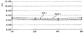
도 2 의 구동 방법에서 채용한 mH 마다의 교류 구동은, 단순히 액정의 장수명화에 기여할 뿐만 아니라 키랄 네마틱 액정을 사용한 액정 표시 장치에서의 표시 특성도 향상시킬 수 있다. 그 이유에 관하여 이하에 설명한다.The AC drive for each mH employed in the driving method of FIG. 2 not only contributes to the long life of the liquid crystal, but also can improve display characteristics in a liquid crystal display device using a chiral nematic liquid crystal. The reason for this is described below.
도 16 은 키랄 네마틱 액정의 문턱전압 Vth, 포화 전압 Vsat 와 온도와의 부의 상관을 나타낸 특성도로서, 문턱전압 Vth, 포화 전압 Vsat 는 온도 의존성을 갖는다. 여기서 Vs 를 선택 기간 T3 중의 주사 신호의 전압 레벨의 절대값으로 하고 Vd 를 선택 기간 T3 중의 데이터 신호의 전압 레벨의 절대값으로 하면 액정의 온 오프 구동 조건은 │Von│=│Vs+Vd│![]()
![]()
![]()
![]()
또한 이 문턱 전압 Vth, 포화 전압 Vsat 는 액정 패널면내에서 분산하는 것으로 알려져 있다.The threshold voltage Vth and the saturation voltage Vsat are also known to be dispersed within the liquid crystal panel plane.
그런데, 포화 전압과 문턱 전압과의 차의 절대값 │Vsat- Vth│이 작으면, 문턱 전압, 포화 전압에 온도 의존성이 있더라도, 또는 면내에서의 비균일성이 있더라도, 온 전압, 오프 전압을 위한 마진을 항상 확보하는 것이 가능하게 된다.By the way, when the absolute value of the difference between the saturation voltage and the threshold voltage Vsat-Vth is small, even if there is a temperature dependence on the threshold voltage, the saturation voltage, or in-plane nonuniformity, It is possible to always secure a margin.
본 발명자등은 │Vsat-Vth│가 반전 시간 mH 에 의존하여 변화하는 것을 발견하였다. 도 17 은 횡축에 반전 시간 mH 를 취하고, 종축에 문턱 전압 Vth. 포화 전압 Vsat 를 취하며, 실험으로 얻은 문턱 전압 Vth, 포화 전압 Vsat 의 mH 의존 특성을 나타내는 것이다. 또한, 이 실험은 듀티 비 = 1/240, 리셋 기간 T1=1.5mS, 리셋 전압 = ±25V, 바이어스 전압 Vd=±1V 로서 상온 아래에서 측정한 것이다.The inventors have found that Vsat-Vth changes depending on the inversion time mH. Fig. 17 shows the inversion time mH on the horizontal axis and threshold voltage Vth on the vertical axis. It takes the saturation voltage Vsat and shows the mH dependent characteristic of the threshold voltage Vth and saturation voltage Vsat obtained by experiment. In addition, this experiment was measured at room temperature with duty ratio = 1/240, reset period T1 = 1.5mS, reset voltage = ± 25V, and bias voltage Vd = ± 1V.
도 18 내지 도 21 의 특성도에 의하면 │Vsat-Vth│가 반전 시간 mH 에 의존하는 것을 보다 명확히 이해할 수 있다.According to the characteristic diagrams of FIGS. 18 to 21, it can be more clearly understood that Vsat-Vth depends on the inversion time mH.
도 18 은 도 17 과 같은 실험을 mH 를 1H~8H(1H=80㎲)로 변화시켜 행한 것이다. 실험 조건은 듀티 비=1/240, 리셋 기간 T1=1.0mS, 리셋 전압=±25V, 바이어스 전압 Vd=±1.3V 로 하고 상온 아래에서 측정한 것이다. 도 18에 의하면 Vth1, 포화 전압 Vsat1 는 2H~4H 의 사이에서 낮아지는 것을 알 수 있다.FIG. 18 is a test performed in the same manner as in FIG. 17 by changing mH to 1H to 8H (1H = 80 Hz). The experimental conditions were measured at room temperature with duty ratio = 1/240, reset period T1 = 1.0mS, reset voltage = ± 25V, bias voltage Vd = ± 1.3V. According to FIG. 18, it turns out that Vth1 and saturation voltage Vsat1 fall between 2H-4H.
도 19 는, 도 18 의 데이터에 기초하여 종축을 │Vsat-Vth│로 한 특성도로서 2H~4H 의 사이에 │Vsat-Vth│가 저하하고 있는 것을 알 수 있다.Fig. 19 is a characteristic diagram in which the vertical axis is | Vsat-Vth | based on the data of Fig. 18, and it can be seen that | Vsat-Vth | is declining between 2H and 4H.
도 20 은 도 19 와 같은 실험을, 듀티비=1/480 의 액정 패널에서 실시한 결과를 나타내고 있다. 1H=40㎲ 이다. 도 20 에 의하면 Vth1, 포화 전압 Vsat1 은, 4H~16H 의 사이에서 낮아지는 것을 알 수 있다.FIG. 20 shows the results of experiments similar to those shown in FIG. 19 in a liquid crystal panel with duty ratio = 1/480. 1H = 40 Hz. According to FIG. 20, it turns out that Vth1 and saturation voltage Vsat1 fall between 4H-16H.
도 21 은 도 20 의 데이터에 기초하여 종축을 │Vsat-Vth│로 한 특성도로서 4H~16H 의 사이에서 │Vsat-Vth│가 저하하고 있음을 알 수 있다.Fig. 21 is a characteristic diagram in which the vertical axis is | Vsat-Vth | on the basis of the data in Fig. 20, and it can be seen that | Vsat-Vth | is declining between 4H and 16H.
이와 같이 mH 를 2H 이상으로 하면, mH=1H 의 경우와 비교하여 │Vsat-Vth│를 작게할 수 있으며 마진을 크게 확보한 상태로 온 전압, 오프 전압을 액정에 인가할 수 있고, 표시 특성을 향상하는 것을 알 수 있다.In this way, when mH is set to 2H or more, │Vsat-Vth│ can be made smaller than in the case of mH = 1H, and the on and off voltages can be applied to the liquid crystal with a large margin. It can be seen that the improvement.
더구나, mH을 2H이상으로 하면, mH=1H의 경우와 비교하여 문턱전압 Vth, 포화전압 Vsat 자체를 저하시키고, 구동전압을 낮게 할 수 있는 효과도 있다.In addition, when mH is 2H or more, the threshold voltage Vth and the saturation voltage Vsat itself can be lowered and the driving voltage can be lowered as compared with the case where mH = 1H.
이와 같은 도 2 의 구동 방법에 의하면 반전 시간 mH 와 표시 특성의 의존성이 확인되었기 때문에 반전 동작에 의해서 액정의 수명과 관계가 깊은 직류의 연속인가를 강하게 억제함과 동시에 표시 특성의 개선도 가능하다.According to such a driving method of FIG. 2, since the dependence of the inversion time mH and the display characteristics is confirmed, the inversion operation can strongly suppress the continuous application of direct current having a long relationship with the lifetime of the liquid crystal, and can also improve the display characteristics.
[도 5의 구동파형의 설명][Description of Drive Waveform of FIG. 5]
도 5는 도 2와 마찬가지로 mH(m=4)의 펄스폭의 FR(도 5(a) 참조)를 사용하여 액정에 인가되는 전압극성을 mH 마다에 반전시키는 방법이나, 주사신호와 데이터 신호의 파형의 각 전압레벨을 변경하였다.FIG. 5 is a method of inverting the voltage polarity applied to the liquid crystal for each mH using FR (see FIG. 5 (a)) having a pulse width of mH (m = 4) similarly to FIG. Each voltage level of the waveform was changed.
주사신호는 도 5(b)에 나타낸 바와 같이, 리셋 기간 T1의 전압은 V4, V5, 지연기간 T2의 전압은 V2, V7, 선택기간 T3의 전압은 V4, V5, 비선택기간 T4의 전압은 V2, V7로 하고 있다.As shown in Fig. 5 (b), the voltage of the reset period T1 is V4, V5, the voltage of the delay period T2 is V2, V7, the voltage of the selection period T3 is V4, V5, and the voltage of the non-selection period T4 is It is set as V2 and V7.
데이터 신호는, 도 5(c)에 나타낸 바와같이, 온전압을 V1, V8, 오프 전압을 V3, V6으로 하고 있다.As shown in Fig. 5C, the data signal has the on voltages V1 and V8 and the off voltages V3 and V6.
이 결과, 매트릭스 표시 화소(i, j)에는, 도 5(d)에 나타난 바와같이, 액정에 인가하는 전압이, 플러스·마이너스로 번갈아 변화하는 것이 된다. 이 도 5의 구동파형을 사용하면 V1~V8을 도 2의 전압 레벨과 똑같이 설정한 경우에는 리셋 전압은 (V4-V8) 또는 (V5-V1)이 되거나, ±23V가 되어 도 2의 경우보다 낮아지지만, 리셋에 필요한 큰 전압을 확보할 수 있다. 다른 전압은 온 전압=±3V, 오프전압=±1V, 바이어스 전압=±1V이 되고, 도 2와 똑같은 전압이 얻어진다. 더욱이 데이터 신호 전위를 그라운드 전압 V1과 최고 전압 V8으로 설정할 수 있으므로, 바이어스 전압이 안정하여, 표시 안정성을 크게 할 있다.As a result, in the matrix display pixels i and j, as shown in Fig. 5 (d), the voltage applied to the liquid crystal alternately changes to plus or minus. Using the drive waveform of FIG. 5, when V1 to V8 are set to the same voltage level as in FIG. 2, the reset voltage is (V4-V8) or (V5-V1) or ± 23V, which is higher than that of FIG. Although lowered, it is possible to secure a large voltage required for reset. The other voltages are on voltage = ± 3V, off voltage = ± 1V, bias voltage = ± 1V, and the same voltage as in FIG. 2 is obtained. Furthermore, since the data signal potential can be set to the ground voltage V1 and the highest voltage V8, the bias voltage is stable, and the display stability can be increased.
또한, 도 5의 경우에는 V3-V2=V2-V1=V8-V7=V7-V6으로 하면 비선택기간 T4의 바이어스 전압이 똑같이 걸리도록 설정할 수 있다. 또한, 도 2와 마찬가지로 온 전압을 크게 하고자 할 때에는, V1과 V2, V7과 V8 간의 전압차를 각각 크게 하면 좋다. 리셋 전압을 크게 하고자 할 때에는, V4와 V5 간의 전위차를 더욱 넓히면 좋다. 나아가서는 이것에 리셋 전압인가 후의 지연시간의 장단을 매기는 데는 선택기간의 타이밍을 1H단위로 시프트시키면 좋다.In the case of Fig. 5, V3-V2 = V2-V1 = V8-V7 = V7-V6 can be set so that the bias voltage of the non-selection period T4 is equally applied. 2, when the on voltage is to be increased, the voltage difference between V1 and V2, V7 and V8 may be increased. When the reset voltage is to be increased, the potential difference between V4 and V5 may be further widened. Further, in order to determine the length of the delay time after applying the reset voltage, the timing of the selection period may be shifted in units of 1H.
[도 6 구동파형의 설명]6 illustrates driving waveforms
도 6은 도 2, 도 5와 똑같이 mH(m=4)마다 반전 동작으로 프레임 단위의 반전 동작을 거듭한 변형례이다.6 is a modified example in which the inversion operation in units of frames is repeated in the inversion operation every mH (m = 4) similarly to FIGS. 2 and 5.
즉, 주사신호 및 데이터 신호 전압레벨을 mH 마다에 반전시켜 가면, 1프레임이 끝나는 단계에서는, 액정에 걸리는 전압이 1프레임내에서는 플러스·마이너스의 밸런스가 취해져 있지 않기 때문에 직류분이 잔류한다. 그래서, 다음 프레임에서는 주사 신호, 데이터 신호의 전압레벨을 앞프레임과 반전시켜 프레임단위로 반전시키고 있다. 즉, 액정에 인가하는 구동파형의 제 n프레임(n은 정수)의 시작전압이, 전압레벨의 제 1군(V1~V4)에 있을 때는, 제(n+1)프레임의 시작은 제 2군(V5~V8)으로 한다. 또한, 제 n 프레임의 시작전압이 제 2군인 때는 제 (n+1)프레임 시작은 제 1군으로 하고, mH마다의 반전에 프레임단위의 반전을 거듭하여 반복하도록 한다. 이것은 프레임마다 반전과 mH 펄스 반전을 조합한 것이라 할 수 있다.In other words, if the scan signal and data signal voltage levels are inverted at every mH, at the end of one frame, since the voltage applied to the liquid crystal does not take a positive or negative balance within one frame, a DC component remains. Therefore, in the next frame, the voltage levels of the scan signal and the data signal are inverted from the previous frame and inverted frame by frame. That is, when the start voltage of the nth frame (n is an integer) of the driving waveform applied to the liquid crystal is in the first group V1 to V4 of the voltage level, the start of the (n + 1) frame is the second group. It is set to (V5 to V8). When the start voltage of the nth frame is the second group, the start of the (n + 1) th frame is the first group, and the inversion of the frame unit is repeated by repeating the inversion for each mH. This is a combination of inversion and mH pulse inversion for each frame.
이 도 6의 구동파형에 의하면 1프레임내에서는 해소하지 못하는 직류분을 2프레임에 걸쳐 완전히 해소할 수 있으므로, 액정의 장수명화에 효과가 크다.According to the driving waveform shown in Fig. 6, since the direct current component which cannot be solved in one frame can be completely solved over two frames, the effect on the life of the liquid crystal is long.
또한 본 실시예는 도 2의 실시예와 동일한 전압으로 설정하였지만, 실시예 2와 동일전압으로 설정하여도 좋다. 도 5의 구동방법에 프레밍 반전을 부가한 구동파형은 도 7에 나타낸 바와 같이 된다.In addition, although this embodiment set the same voltage as the embodiment of FIG. 2, you may set it to the same voltage as Example 2. As shown in FIG. The driving waveform in which the framing inversion is added to the driving method of FIG. 5 is as shown in FIG.
[액정구동회로의 설명][Explanation of liquid crystal drive circuit]
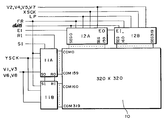
도 8 내지 도 12에, 도 2, 5, 6, 7의 구동파형을 실현하기 위한 실제의 액정구동회로의 구성 및 타임챠트를 나타낸다. 도 8은 액정 패널 및 그 구동회로를 포함하는 표시장치의 전체 구성도이다. 액정 패널(10)은 320×320 화소를 가지며 이 액정패널(10)을 구동하기 위해 도 1, 도 2의 Y드라이버 회로(11A,11B) 및 제 1, 제 2 X드라이버 회로(12A,12B)가 설정되어 있다.8 to 12 show the configuration and time chart of an actual liquid crystal drive circuit for realizing the drive waveforms of FIGS. 2, 5, 6, and 7. 8 is an overall configuration diagram of a display device including a liquid crystal panel and a driving circuit thereof. The
제 1, 제 2 Y드라이버회로는 각각 동일한 구성을 가지며 그 상세한 것이 도 9에 도시되어 있다.Each of the first and second Y driver circuits has the same configuration, and details thereof are shown in FIG.
Y드라이버 회로(11A)에 관하여 도 9를 참조하여 설명한다. Y드라이버 회로(11A)는 리셋용 시프트 레지스터(13A), 셀렉트용 시프트 레지스터(13B)의 2개의 시프트레지스터를 가지며, 각각에는 160단위의 레지스터가 있다. 리셋용 레지스터(13A)에는 리셋기간 T1을 지정한 리셋신호 RI가 입력되고, 이 신호는 시프트 클록(YSCK)에 의해 다음 단의 레지스터에 축차 시프트되고 있다. 또한, 160단번째의 레지스터 내용은 출력단자 RO를 통해서 출력되고 제 2 Y드라이버 회로의 입력(RI)이 되는 캐스케이드 접속이 이루어진다. 셀렉트용 시프트 레지스터(13B)에 관해서도 마찬가지이며, 셀렉트 기간 T3을 지정한 신호 SI가 시프트 레지스터(13B)에 입력되고, 그리고 나서 신호는 시프트 클록(YSCK)에 의해 다음 단의 레지스터에 차례로 전달되어 간다. 최종 단(160)의 레지스터 내용은 출력단자(SO)를 통해서 다음 제 2 Y드라이버 회로(11B)의 입력 신호(SI)가 되며, 캐스케이드 접속이 이루어진다.The Y driver circuit 11A will be described with reference to FIG. The Y driver circuit 11A has two shift registers, a
각 시프트 레지스터(13A,13B)의 내용은, 160채널 동시에 병렬출력되어 출력 컨트롤러(14)에 입력된다. 이 출력 컨트롤러(14)에 리셋 신호 Q, 셀렉트신호 S 및 교류화 신호 FR의 입력상태에 의해서 6개 상태 즉 R, S, FR=(0, 0, 0) 또는 (0, 0, 1) 또는 (0, 1, 0) 또는 (0, 1, 1) 또는 (1, 0, 0) 또는 (1, 0, 1)을 구별한 신호를 출력한다. 이 신호는 레벨 시프터(15)를 통해서 Y드라이버(16)에 입력된다.The contents of each
이 Y드라이버(16)에는 4종류의 구동전압(V1, V3, V6, V8) 또는 (V2, V4, V5, V7)이 입력되어 있으며, 출력 컨트롤러(14)에서 구별한 6개m이 상태에 기초하여, 도 24에 보인 진리값표에 따라 어느 1개의 구동전압을 각 채널마다에 출력한다. 또한, 도 24에서, Yout1은 도 2, 6에 대응한 구동파형을 얻을 때의 선택을, 또한 Yout2는 도 5, 7에 대응한 구동파형을 얻을 때의 선택을 도시한다.Four types of driving voltages (V1, V3, V6, V8) or (V2, V4, V5, V7) are input to the
도 11은 Y드라이브 회로에 입출력되는 각 신호 상태를 일부 나타낸 타이밍도이다. 도 11에 나타낸 타이밍차트의 경우, 선택기간 T3의 길이를 1H로한 때 시프트 클록(YSCK)은 1H마다 H/L을 반복하는 신호가 되어 있고, 교류화 신호(FR)는 mH로 되어 있으므로, 도 2, 5와 같이 mH마다에 액정에 인가되는 전압 극성이 반전하는 주사신호(YK)가 된다.11 is a timing diagram partially illustrating each signal state input and output to the Y drive circuit. In the case of the timing chart shown in Fig. 11, when the length of the selection period T3 is 1H, the shift clock YSCK becomes a signal for repeating H / L every 1H, and the AC signal FR is mH. As shown in 2 and 5, a scan signal YK is obtained in which the voltage polarity applied to the liquid crystal is reversed every mH.
다음에, 제 1 X드라이버 회로(12A)에 관하여 도 10을 참조하여 설명한다. X드라이버 회로(12A)는 160단 레지스터로 구성되는 시프트 레지스터(17)를 가지며, 입력신호(EI)를 시프트 클록(XSCK)을 따라 다음단의 레지스터에 축차 시프트해 간다. 160번째 레지스터 내용은 EO 출력단을 통해서 외부로 출력되고, 제 2X 드라이버 회로(12B)와 캐스케이드 계속이 가능하다. 시프트 레지스터(17)에 입력되는 신호(EI)는 도 12도에 나타낸 바와 같이 1수평주사기간(1H)에 1회 논리의 1이 되는 신호이다. 따라서 시프트 레지스터(17)의 각 레지스터에서 논리의 1 이 축차 출력되는 것이므로, 도 1의 래치회로(18)는 각 레지스터와 대응하는 어드레스에 화상데이터를 래치하게 된다. 이 도 1의 래치회로(18)의 160 채널의 데이터는, 래치펄스(LP)가 입력하는 타이밍에서 제 2 래치회로(19)에 동시에 래치된다. 교류화신호(FR) 및 도 2의 래치회로(19)로부터 데이터를 입력하는 출력 콘트롤러 회로(20)는, 데이터(D)와 교류화 신호(FR)의 입력 상태에 의해서 4개 상태(D,FR)=(0,0) 또는 (0,1) 또는 (1,0) 또는 (1,1)을 구별한 신호를, 레벨 시프터(21)를 개재(介在)하여 각 채널 마다 X드라이버(22)에 입력시킨다. X드라이버(22)는 4종류의 구동전압, 즉(V2, V4, V5, V7) 또는 (V1, V3, V6, V8)을 입력으로하고, 출력 콘트롤러 회로(20)로부터의 정보에 기초하여 이들중 1개의 전압을 선별출력한다. 도 25에 그 진리값표를 나타내고 있다. 또한, 도 25에서 XOUT1은 도 2와 6에, XOUT2는 도 5와 7의 실시예에 대응하고 있다.Next, the first X driver circuit 12A will be described with reference to FIG. The X driver circuit 12A has a shift register 17 composed of 160 stage registers, and sequentially shifts the input signal EI to the next stage register along the shift clock XSCK. The 160th register contents are output to the outside through the EO output stage, and the cascade continues with the 2X driver circuit 12B. The signal EI input to the shift register 17 is a signal that becomes one logic once in one horizontal scanning period 1H, as shown in FIG. Therefore, since one of the logics is sequentially output from each register of the shift register 17, the
[전원회로의 설명][Description of Power Supply Circuit]
도 8에서 도 12에 나타낸 회로에서 사용하는 전원회로의 실시예에 관하여 설명한다. 본 발명에서는 주사신호, 데이터 신호의 각종전압 레벨을 설정하기 위해 총 8레벨의 전위를 사용하고 있다. 이 중 V1=GND, V8=최대기준 구동전압(VH)으로 하면 나머지 중간의 V2~V7에 대해 전위를 결정하면 좋다. 이하에 설명하는 각 전원회로는, 다수 전압 레벨로 분리된 구동전위를, 1개의 볼륨에 의해 모두 동시에 가변으로 하는 것이 가능하고 표시의 최적의 조정에는 가장 간편한 전원회로이다.An embodiment of a power supply circuit used in the circuit shown in Figs. 8 to 12 will be described. In the present invention, a total of eight levels of potentials are used to set various voltage levels of the scan signal and the data signal. If V1 = GND and V8 = maximum reference drive voltage (VH), the potential can be determined for the remaining intermediate V2 to V7. Each of the power supply circuits described below is capable of simultaneously varying the driving potentials separated by a plurality of voltage levels by one volume, and is the power supply circuit that is the easiest for optimal adjustment of display.
먼저, 전압 평균법으로 비선택기간중의 바이어스 전압이 되는 기준 전위차(VB)를 데이터 신호의 Von, Voff에서 다음과 같이 정의하여 일정하게 되도록 한다.First, the reference potential difference VB, which becomes the bias voltage during the non-selection period, is defined by the voltage average method as follows in Von and Voff of the data signal so as to be constant.
VB=│Von-Voff│/2VB = │Von-Voff│ / 2
이 기준 전위차(VB)를 기준으로 전원회로를 실현한 것이 도 13이다.13 shows a power supply circuit based on this reference potential difference VB.
VB는 수 V이면 충분하므로, 예컨대 고전압(VH)으로부터 제너다이오드(30)로 전위를 낮추고 또한 이 전위에서 가변저항(32)의 중전전위를 임의로 인출하여, 기준전위차(VB)로 한다. 필요한 전압(V2, V3, V4)은 이 VB를 1내지~수배로 증폭한 것을 V1에 가하면 좋기 때문에 도시한 바와같이, 정의 증폭회로를 오피앰프로 구성하고, V2=V1+VB, V3=V1+VB, V4=V1+aVB(a는 증폭률)로 한다. 증폭률 a는 V4의 전압을 출력하는 오피앰프의 피드백 저항(34)에 의해 결정하며 이 저항값을 가변으로하면, 증폭률 a를 임의로 설정할 수 있다.Since VB is sufficient for several V, for example, the potential is lowered from the high voltage VH to the
다음에 이들 출력과 최고전위 VH의 감산회로를 오피앰프로 구성하고 V7=VH-V2, V6=VH=V3, V5=VH-V4로 하면 VB를 바꾸는 것만으로 모든 전압 레벨이 연동하여 변하는 바이어스 일정한 전원이 된다. 실제로는 주사신호 및 데이터 신호의 드라이버 회로에 입력시키기 전에, 버퍼를 개재시키면, 이 버퍼에 의해 각 전압레벨을 증폭할 수 있다.Next, if these outputs and the subtraction circuit of the highest potential VH are configured as an op amp, and V7 = VH-V2, V6 = VH = V3, and V5 = VH-V4, all the voltage levels are linked together to change the bias constant. It becomes the power source. In fact, before inputting the scan signal and the data signal to the driver circuit, the buffers can be amplified to amplify each voltage level.
본 전원회로는 증폭률 a를 변경하는 것으로 V4, V5를 최적으로 조정할 수 있으며, 도 5, 7의 실시예의 온 전압(V1-V4 또는 V8-V5)을 소망대로 조정할 수 있다. 또한 증폭배율을 (a-2), (a-1), a가 되도록 V2, V3, V4를 정하면, 도 2, 6의 실시예에 적합하게 된다.The power supply circuit can adjust V4 and V5 optimally by changing the amplification factor a, and can adjust the on voltages V1-V4 or V8-V5 of the embodiments of FIGS. 5 and 7 as desired. Further, when V2, V3, and V4 are determined so that the amplification magnification is (a-2), (a-1), and a, the embodiments of Figs. 2 and 6 are suitable.
도 14는 V3=b B, V2=(b-1) VB, V4=(b+1)VB가 되도록 오피앰프로 연산회로를 구성하여 V2~V4의 전위를 작성한 것이다. 다만 b는 증폭률이며 b는 1이상의 수치, 더욱 바람직하게는 2이상의 수치이다. V5~V7에 관해서는 도 13과 마찬가지로, VH(V8)에서 각각 V4, V3, V2를 오피앰프로 구성한 감산회로로 감산하여 작성하고 있다. 여기서 도 14에서는 V3의 전압을 출력하는 오피앰프의 피드백 저항(34)을 가변저항으로 하고 증폭률 b의 값을 자유롭게 바꿀 수 있도록 하고 있다. 이 결과, V4, V5의 각 전압 레벨을 조정할 수 있다. 따라서 도 2, 6의 실시예의 온전압(V1-V4 또는 V8-V5)을 소망대로 조정할 수 있다. 이와 같이, 액정에 인가되는 온전압을 간단히 조작하는 것이 가능하고 이것도 구동회로 조정에 유효하게 된다.Fig. 14 shows an operational circuit composed of an op amp so that V3 = b B, V2 = (b-1) VB, and V4 = (b + 1) VB to create potentials of V2 to V4. B is an amplification factor and b is a value of 1 or more, more preferably 2 or more. As for Fig. 13, V5 to V7 are created by subtracting V4, V3, and V2 from the VH (V8) with a subtraction circuit composed of an op amp. In FIG. 14, the
도 15는 본 발명의 또다른 전원회로를 나타내고 있다. 동도면에서, 7개의 저항기(R1, R2 ... R7)가 설정되고, 이 라인의 일단에는 최대 전압 레벨 V8을 생성하는 전압 발생회로(40)가 접속되며, 다른 단이 그라운드 전압 레벨 V1로 되어 있다. 그러므로 인접한 2개의 저항기 간에는 저항기(R1, R2 ... R7)에서 순차로 전압강하되어 얻어지는 전압레벨(V7~V2)을 출력하는 6개의 전압출력단자(OUT7~OUT2)가 마련되어 있다. V5의 전압출력단자(OUT5)와 V4의 전압 출력단자(OUT4)와의 사이의 저항기 R4는 가변저항기이며 그 저항값을 외부에서 변경할 수 있다.Fig. 15 shows another power supply circuit of the present invention. In the same figure, seven resistors R1, R2 ... R7 are set, and one end of this line is connected with a
이 전원회로에서는, 저항기(R4)의 저항값의 변경에 의해서 각 저항기(R1~R7)를 흐르는 전류값을 변경할 수 있으며, 강하전압의 크기를 변경할 수 있기 때문에, 그라운드 전압레벨(V1)과 최대 전압레벨(V8)을 제외한 각 전압레벨(V2~V7)을 동시에 조정가능하게 된다. 또한 전압 발생회로(40)에서 V8의 크기를 변경하면 V2~V8을 임의로 변경하는 것이 가능하게 된다. 또한, 도 14, 도 15에서, V2~V7의 전압 레벨이 출력하는 OUT2~OUT7에는 각각 증폭용 오피앰프가 접속되는 경우도 있다. 또한, 본 발명은 상기 실시예에 한정되는 것은 아니며 본 발명의 요지의 범위내에서 여러 가지의 변형 실시가 가능하다. 예컨대 도 2, 도 6에 나타낸 실시예에서는, 반전시간을 결정하는 값 m과 디스플레이 주사 라인 수 n의 사이에 최대 공약수가 없도록 설정하면 반전 위치가 자연스럽게 어긋나며, 반전으로 인한 파형 왜곡이나 크로스토크를 눈에 띄지 않게 하는 것이 가능하다. 또한 m을 적당하게 크게하면 전압반전으로 발생하는 크로스토크 위치가 적어지는 효과도 있다.In this power supply circuit, the current value flowing through each of the resistors R1 to R7 can be changed by changing the resistance value of the resistor R4, and the magnitude of the drop voltage can be changed. Therefore, the ground voltage level V1 and the maximum value can be changed. Each voltage level V2 to V7 except the voltage level V8 can be adjusted simultaneously. In addition, when the size of V8 is changed in the
Claims (18)
Applications Claiming Priority (3)
| Application Number | Priority Date | Filing Date | Title |
|---|---|---|---|
| JP95-118131 | 1995-05-17 | ||
| JP11813195 | 1995-05-17 | ||
| PCT/JP1995/001835 WO1996036902A1 (en) | 1995-05-17 | 1995-09-14 | Liquid crystal display, its driving method, and driving circuit and power supply used therefor |
Publications (1)
| Publication Number | Publication Date |
|---|---|
| KR100254647B1 true KR100254647B1 (en) | 2000-05-01 |
Family
ID=14728818
Family Applications (1)
| Application Number | Title | Priority Date | Filing Date |
|---|---|---|---|
| KR1019970700243A KR100254647B1 (en) | 1995-05-17 | 1995-09-14 | Liquid crystal display device and its drive method and the drive circuit and power supply circuit used therein |
Country Status (9)
| Country | Link |
|---|---|
| US (1) | US6252571B1 (en) |
| EP (1) | EP0772067B1 (en) |
| JP (1) | JP3577719B2 (en) |
| KR (1) | KR100254647B1 (en) |
| CN (1) | CN1156815C (en) |
| DE (1) | DE69526505T2 (en) |
| HK (1) | HK1021612A1 (en) |
| TW (1) | TW316307B (en) |
| WO (1) | WO1996036902A1 (en) |
Families Citing this family (21)
| Publication number | Priority date | Publication date | Assignee | Title |
|---|---|---|---|---|
| GB9717597D0 (en) * | 1997-08-21 | 1997-10-22 | Sharp Kk | Liquid crystal device |
| JP3659013B2 (en) * | 1997-10-22 | 2005-06-15 | セイコーエプソン株式会社 | Liquid crystal device, driving method thereof and electronic apparatus using the same |
| US6414669B1 (en) | 1998-05-14 | 2002-07-02 | Minolta Co., Ltd. | Driving method and apparatus for liquid crystal display device |
| JP3713954B2 (en) * | 1998-05-14 | 2005-11-09 | コニカミノルタホールディングス株式会社 | Driving method of liquid crystal display element |
| US6927765B1 (en) * | 1998-11-17 | 2005-08-09 | Minolta Co., Ltd. | Liquid crystal display device and driving method thereof |
| EP1130568A3 (en) | 2000-03-01 | 2003-09-10 | Minolta Co., Ltd. | Liquid crystal display device |
| CN102789764B (en) * | 2001-11-20 | 2015-05-27 | 伊英克公司 | Methods for driving bistable electro-optic displays |
| EP1324308A1 (en) * | 2001-12-27 | 2003-07-02 | STMicroelectronics S.r.l. | Generation system for driving voltages of the rows and of the columns of a liquid crystal display |
| FR2835644B1 (en) * | 2002-02-06 | 2005-04-29 | Nemoptic | METHOD AND DEVICE FOR ADDRESSING A BISTABLE LIQUID CRYSTAL SCREEN |
| JP4169992B2 (en) * | 2002-02-27 | 2008-10-22 | シャープ株式会社 | Liquid crystal display device and driving method thereof |
| JP4015908B2 (en) * | 2002-08-29 | 2007-11-28 | 松下電器産業株式会社 | Display device drive circuit and display device |
| JP4366914B2 (en) * | 2002-09-25 | 2009-11-18 | 日本電気株式会社 | Display device drive circuit and display device using the same |
| JP4543632B2 (en) * | 2003-08-07 | 2010-09-15 | 日本電気株式会社 | Liquid crystal display device and liquid crystal display device driving method |
| JP2007507727A (en) * | 2003-09-29 | 2007-03-29 | コーニンクレッカ フィリップス エレクトロニクス エヌ ヴィ | Bistable display with proper gradation and natural image updates |
| US7545396B2 (en) * | 2005-06-16 | 2009-06-09 | Aurora Systems, Inc. | Asynchronous display driving scheme and display |
| WO2007108574A1 (en) * | 2006-03-23 | 2007-09-27 | Anapass Inc. | Display, timing controller and data driver for transmitting serialized multi-level data signal |
| KR100661828B1 (en) * | 2006-03-23 | 2006-12-27 | 주식회사 아나패스 | Display, timing controller and data driver for transmitting serialized multi-level data signal |
| EP2104094A1 (en) * | 2008-03-17 | 2009-09-23 | The Swatch Group Research and Development Ltd. | Display device capable of operating in partial low-power display mode |
| US9024964B2 (en) | 2008-06-06 | 2015-05-05 | Omnivision Technologies, Inc. | System and method for dithering video data |
| CN102208175B (en) * | 2010-03-29 | 2016-01-20 | 精工电子有限公司 | The driving method of bistable liquid crystal display device |
| CN110738973A (en) * | 2019-09-09 | 2020-01-31 | 福建华佳彩有限公司 | panel driving method |
Citations (3)
| Publication number | Priority date | Publication date | Assignee | Title |
|---|---|---|---|---|
| JPS6368819A (en) * | 1986-09-10 | 1988-03-28 | Casio Comput Co Ltd | Generating circuit for liquid crystal driving voltage |
| JPS6381328A (en) * | 1986-09-26 | 1988-04-12 | Hitachi Ltd | Power source circuit for driving liquid crystal display unit |
| JPH01216323A (en) * | 1988-02-24 | 1989-08-30 | Seiko Epson Corp | Liquid crystal display device |
Family Cites Families (48)
| Publication number | Priority date | Publication date | Assignee | Title |
|---|---|---|---|---|
| IT946051B (en) | 1970-12-04 | 1973-05-21 | Hoffmann La Roche | OPTICAL CELL |
| US3837730A (en) | 1973-11-28 | 1974-09-24 | Bell Telephone Labor Inc | Matrix-addressed liquid crystal display |
| JPS5341199A (en) | 1976-08-31 | 1978-04-14 | Sharp Corp | Liquid crystal color display unit |
| US4239345A (en) | 1979-04-16 | 1980-12-16 | Bell Telephone Laboratories, Incorporated | Bistable liquid crystal twist cell |
| US4333708A (en) | 1979-11-30 | 1982-06-08 | Bell Telephone Laboratories, Incorporated | Mechanically multistable liquid crystal cell |
| US4367924A (en) | 1980-01-08 | 1983-01-11 | Clark Noel A | Chiral smectic C or H liquid crystal electro-optical device |
| US4505548A (en) | 1980-10-20 | 1985-03-19 | At&T Bell Laboratories | Bistable liquid crystal twist cell |
| US4529271A (en) | 1982-03-12 | 1985-07-16 | At&T Bell Laboratories | Matrix addressed bistable liquid crystal display |
| US4717243A (en) | 1982-08-25 | 1988-01-05 | American Telephone And Telegraph Company, At&T Bell Laboratories | Bistable liquid crystal display utilizing priming voltages |
| FR2532453A1 (en) | 1982-08-25 | 1984-03-02 | Western Electric Co | Bistable liquid crystal display device using preparation voltages |
| US4601542A (en) | 1982-10-15 | 1986-07-22 | At&T Bell Laboratories | Nematic liquid crystal storage display device |
| US4601543A (en) | 1982-10-15 | 1986-07-22 | At&T Bell Laboratories | Nematic liquid crystal storage display device |
| US4601544A (en) | 1982-10-15 | 1986-07-22 | At&T Bell Laboratories | Nematic liquid crystal storage display device |
| US4582396A (en) | 1983-05-09 | 1986-04-15 | Tektronix, Inc. | Field sequential color display system using optical retardation |
| US4566758A (en) | 1983-05-09 | 1986-01-28 | Tektronix, Inc. | Rapid starting, high-speed liquid crystal variable optical retarder |
| IN161652B (en) | 1983-07-12 | 1988-01-09 | Bbc Brown Boveri & Cie | |
| US4664483A (en) | 1984-02-24 | 1987-05-12 | U.S. Philips Corporation | Liquid crystal display device with a hysteresis |
| US4701026A (en) | 1984-06-11 | 1987-10-20 | Seiko Epson Kabushiki Kaisha | Method and circuits for driving a liquid crystal display device |
| GB2173337B (en) | 1985-04-03 | 1989-01-11 | Stc Plc | Addressing liquid crystal cells |
| US4850676A (en) | 1985-07-31 | 1989-07-25 | Seiko Epson Corporation | Method for driving a liquid crystal element |
| US4770500A (en) | 1986-06-10 | 1988-09-13 | Kaiser Aerospace And Electronics Corporation | Method and apparatus for multi color display |
| US5189535A (en) | 1986-12-11 | 1993-02-23 | Fujitsu Limited | Liquid crystal display element and method for driving same |
| US4952032A (en) | 1987-03-31 | 1990-08-28 | Canon Kabushiki Kaisha | Display device |
| US5010328A (en) | 1987-07-21 | 1991-04-23 | Thorn Emi Plc | Display device |
| NL8701831A (en) | 1987-08-04 | 1989-03-01 | Philips Nv | OSCILLATOR WITH FREQUENCY STABILIZERS. |
| JPH078581B2 (en) | 1987-09-14 | 1995-02-01 | 株式会社日立製作所 | Liquid crystal optical switch driving method |
| JP2770365B2 (en) | 1989-01-17 | 1998-07-02 | 富士通株式会社 | Liquid crystal display device |
| GB2233106B (en) | 1989-05-23 | 1993-08-25 | Citizen Watch Co Ltd | Ferroelectric liquid crystal element and method of driving the same |
| US5065695A (en) | 1989-06-16 | 1991-11-19 | Nordson Corporation | Apparatus for compensating for non-linear flow characteristics in dispensing a coating material |
| JPH03125119A (en) | 1989-10-09 | 1991-05-28 | Sharp Corp | Driving method for liquid crystal element |
| JPH03177817A (en) | 1989-12-06 | 1991-08-01 | Toshiba Corp | Active matrix type liquid crystal display element |
| US5168270A (en) * | 1990-05-16 | 1992-12-01 | Nippon Telegraph And Telephone Corporation | Liquid crystal display device capable of selecting display definition modes, and driving method therefor |
| JPH04113314A (en) * | 1990-09-03 | 1992-04-14 | Sharp Corp | Liquid crystal display device |
| JP2659473B2 (en) * | 1990-09-28 | 1997-09-30 | 富士通株式会社 | Display panel drive circuit |
| GB2249653B (en) | 1990-10-01 | 1994-09-07 | Marconi Gec Ltd | Ferroelectric liquid crystal devices |
| JP2695981B2 (en) * | 1990-10-05 | 1998-01-14 | 株式会社東芝 | LCD drive power supply circuit |
| JP2794499B2 (en) | 1991-03-26 | 1998-09-03 | 株式会社半導体エネルギー研究所 | Method for manufacturing semiconductor device |
| JPH0535200A (en) * | 1991-07-31 | 1993-02-12 | Hitachi Ltd | Display device and its driving method |
| JPH0537057A (en) | 1991-07-31 | 1993-02-12 | Mitsubishi Electric Corp | Gas laser |
| DE69220173T2 (en) | 1991-10-07 | 1997-09-18 | Fujitsu Ltd | Method for controlling a surface stabilized ferroelectric liquid crystal display element to increase the gray level number |
| KR950000754B1 (en) | 1992-04-30 | 1995-01-28 | 삼성전관 주식회사 | Driving method and vias voltage circuit of strong dielectric lcd using stn driving i. c. |
| EP0569029B1 (en) | 1992-05-07 | 1998-04-22 | Seiko Epson Corporation | Liquid crystal display device having two metastable states and its driving method |
| JP3753440B2 (en) | 1992-05-07 | 2006-03-08 | セイコーエプソン株式会社 | Liquid crystal display device and driving method of liquid crystal display device |
| US5251048A (en) | 1992-05-18 | 1993-10-05 | Kent State University | Method and apparatus for electronic switching of a reflective color display |
| JP3634390B2 (en) | 1992-07-16 | 2005-03-30 | セイコーエプソン株式会社 | Liquid crystal electro-optic element |
| DE69430687T2 (en) | 1993-02-10 | 2002-11-21 | Seiko Epson Corp | ACTIVE MATRIX SUBSTRATE AND THIN FILM TRANSISTOR AND METHOD FOR PRODUCTION |
| JP3489169B2 (en) * | 1993-02-25 | 2004-01-19 | セイコーエプソン株式会社 | Driving method of liquid crystal display device |
| JP3177817B2 (en) | 1995-06-13 | 2001-06-18 | 本田技研工業株式会社 | Travel guidance device for vehicles |
-
1995
- 1995-09-14 CN CNB951941712A patent/CN1156815C/en not_active Expired - Fee Related
- 1995-09-14 EP EP95931415A patent/EP0772067B1/en not_active Expired - Lifetime
- 1995-09-14 WO PCT/JP1995/001835 patent/WO1996036902A1/en active IP Right Grant
- 1995-09-14 US US08/765,894 patent/US6252571B1/en not_active Expired - Lifetime
- 1995-09-14 JP JP50938196A patent/JP3577719B2/en not_active Expired - Fee Related
- 1995-09-14 DE DE69526505T patent/DE69526505T2/en not_active Expired - Lifetime
- 1995-09-14 KR KR1019970700243A patent/KR100254647B1/en active IP Right Grant
- 1995-10-06 TW TW084110537A patent/TW316307B/zh not_active IP Right Cessation
-
1998
- 1998-12-24 HK HK98115546A patent/HK1021612A1/en not_active IP Right Cessation
Patent Citations (3)
| Publication number | Priority date | Publication date | Assignee | Title |
|---|---|---|---|---|
| JPS6368819A (en) * | 1986-09-10 | 1988-03-28 | Casio Comput Co Ltd | Generating circuit for liquid crystal driving voltage |
| JPS6381328A (en) * | 1986-09-26 | 1988-04-12 | Hitachi Ltd | Power source circuit for driving liquid crystal display unit |
| JPH01216323A (en) * | 1988-02-24 | 1989-08-30 | Seiko Epson Corp | Liquid crystal display device |
Also Published As
| Publication number | Publication date |
|---|---|
| DE69526505D1 (en) | 2002-05-29 |
| US6252571B1 (en) | 2001-06-26 |
| DE69526505T2 (en) | 2002-10-31 |
| HK1021612A1 (en) | 2000-06-16 |
| TW316307B (en) | 1997-09-21 |
| WO1996036902A1 (en) | 1996-11-21 |
| EP0772067B1 (en) | 2002-04-24 |
| EP0772067A4 (en) | 1999-03-17 |
| CN1152962A (en) | 1997-06-25 |
| JP3577719B2 (en) | 2004-10-13 |
| EP0772067A1 (en) | 1997-05-07 |
| CN1156815C (en) | 2004-07-07 |
Similar Documents
| Publication | Publication Date | Title |
|---|---|---|
| KR100254647B1 (en) | Liquid crystal display device and its drive method and the drive circuit and power supply circuit used therein | |
| KR100238903B1 (en) | Lcd device driving method | |
| KR100654824B1 (en) | Method for driving electro-optical apparatus, electro-optical apparatus, and electronic equipment | |
| US7362299B2 (en) | Liquid crystal display device, driving circuit for the same and driving method for the same | |
| US5760757A (en) | Negative feeback control of dummy row electrodes to reduce crosstalk and distortion in scan electrodes induced by signal electrode fluctuations | |
| JPH0695625A (en) | Driving method for ferroelectric liquid crystal display element and bias voltage circuit therefor | |
| US5724060A (en) | Multiplex addressing of ferro-electric liquid crystal displays | |
| WO1996035976A1 (en) | Method of driving antiferroelectric liquid crystal display and apparatus therefor | |
| US5805130A (en) | Liquid crystal display device and method for driving the same | |
| EP0238287A2 (en) | Ferro-electric liquid crystal electro-optical device | |
| JP4049192B2 (en) | Electro-optical device driving method, electro-optical device, and electronic apparatus | |
| JP2001504954A (en) | Display device | |
| US8743041B2 (en) | Liquid crystal display drive circuit and liquid crystal display device | |
| JP3555578B2 (en) | Driving method of liquid crystal display device | |
| JP3525895B2 (en) | Driving method of liquid crystal display device | |
| US20210241710A1 (en) | Liquid crystal display device and drive method thereof | |
| KR100864974B1 (en) | Liquid crystal display | |
| WO1997043750A1 (en) | Super-twisted nematic liquid crystal display driving circuit adopting multiple line selection method using pulse width modulation | |
| KR20050085067A (en) | Liquid crystal display device | |
| JP2004361689A (en) | Driving method of antiferroelectric liquid crystal panel | |
| US20030151583A1 (en) | Display driver circuit, electro-optical device, and display drive method | |
| JPH08248374A (en) | Waveform display device | |
| JP3776113B2 (en) | Driving circuit for liquid crystal display device | |
| JP3513016B2 (en) | Driving method and driving circuit for liquid crystal display device | |
| JPH07128641A (en) | Liquid crystal display device |
Legal Events
| Date | Code | Title | Description |
|---|---|---|---|
| A201 | Request for examination | ||
| E902 | Notification of reason for refusal | ||
| E701 | Decision to grant or registration of patent right | ||
| GRNT | Written decision to grant | ||
| FPAY | Annual fee payment |
Payment date: 20130118 Year of fee payment: 14 |
|
| FPAY | Annual fee payment |
Payment date: 20140117 Year of fee payment: 15 |
|
| FPAY | Annual fee payment |
Payment date: 20150120 Year of fee payment: 16 |