JP3577719B2 - Liquid crystal display device, driving method thereof, and driving circuit used therefor - Google Patents
Liquid crystal display device, driving method thereof, and driving circuit used therefor Download PDFInfo
- Publication number
- JP3577719B2 JP3577719B2 JP50938196A JP50938196A JP3577719B2 JP 3577719 B2 JP3577719 B2 JP 3577719B2 JP 50938196 A JP50938196 A JP 50938196A JP 50938196 A JP50938196 A JP 50938196A JP 3577719 B2 JP3577719 B2 JP 3577719B2
- Authority
- JP
- Japan
- Prior art keywords
- voltage
- group
- liquid crystal
- voltage level
- selection
- Prior art date
- Legal status (The legal status is an assumption and is not a legal conclusion. Google has not performed a legal analysis and makes no representation as to the accuracy of the status listed.)
- Expired - Fee Related
Links
Images


Classifications
-
- G—PHYSICS
- G09—EDUCATION; CRYPTOGRAPHY; DISPLAY; ADVERTISING; SEALS
- G09G—ARRANGEMENTS OR CIRCUITS FOR CONTROL OF INDICATING DEVICES USING STATIC MEANS TO PRESENT VARIABLE INFORMATION
- G09G3/00—Control arrangements or circuits, of interest only in connection with visual indicators other than cathode-ray tubes
- G09G3/20—Control arrangements or circuits, of interest only in connection with visual indicators other than cathode-ray tubes for presentation of an assembly of a number of characters, e.g. a page, by composing the assembly by combination of individual elements arranged in a matrix no fixed position being assigned to or needed to be assigned to the individual characters or partial characters
- G09G3/34—Control arrangements or circuits, of interest only in connection with visual indicators other than cathode-ray tubes for presentation of an assembly of a number of characters, e.g. a page, by composing the assembly by combination of individual elements arranged in a matrix no fixed position being assigned to or needed to be assigned to the individual characters or partial characters by control of light from an independent source
- G09G3/36—Control arrangements or circuits, of interest only in connection with visual indicators other than cathode-ray tubes for presentation of an assembly of a number of characters, e.g. a page, by composing the assembly by combination of individual elements arranged in a matrix no fixed position being assigned to or needed to be assigned to the individual characters or partial characters by control of light from an independent source using liquid crystals
- G09G3/3611—Control of matrices with row and column drivers
- G09G3/3622—Control of matrices with row and column drivers using a passive matrix
- G09G3/3629—Control of matrices with row and column drivers using a passive matrix using liquid crystals having memory effects, e.g. ferroelectric liquid crystals
-
- G—PHYSICS
- G09—EDUCATION; CRYPTOGRAPHY; DISPLAY; ADVERTISING; SEALS
- G09G—ARRANGEMENTS OR CIRCUITS FOR CONTROL OF INDICATING DEVICES USING STATIC MEANS TO PRESENT VARIABLE INFORMATION
- G09G3/00—Control arrangements or circuits, of interest only in connection with visual indicators other than cathode-ray tubes
- G09G3/20—Control arrangements or circuits, of interest only in connection with visual indicators other than cathode-ray tubes for presentation of an assembly of a number of characters, e.g. a page, by composing the assembly by combination of individual elements arranged in a matrix no fixed position being assigned to or needed to be assigned to the individual characters or partial characters
- G09G3/34—Control arrangements or circuits, of interest only in connection with visual indicators other than cathode-ray tubes for presentation of an assembly of a number of characters, e.g. a page, by composing the assembly by combination of individual elements arranged in a matrix no fixed position being assigned to or needed to be assigned to the individual characters or partial characters by control of light from an independent source
- G09G3/36—Control arrangements or circuits, of interest only in connection with visual indicators other than cathode-ray tubes for presentation of an assembly of a number of characters, e.g. a page, by composing the assembly by combination of individual elements arranged in a matrix no fixed position being assigned to or needed to be assigned to the individual characters or partial characters by control of light from an independent source using liquid crystals
- G09G3/3611—Control of matrices with row and column drivers
- G09G3/3674—Details of drivers for scan electrodes
- G09G3/3681—Details of drivers for scan electrodes suitable for passive matrices only
-
- G—PHYSICS
- G09—EDUCATION; CRYPTOGRAPHY; DISPLAY; ADVERTISING; SEALS
- G09G—ARRANGEMENTS OR CIRCUITS FOR CONTROL OF INDICATING DEVICES USING STATIC MEANS TO PRESENT VARIABLE INFORMATION
- G09G3/00—Control arrangements or circuits, of interest only in connection with visual indicators other than cathode-ray tubes
- G09G3/20—Control arrangements or circuits, of interest only in connection with visual indicators other than cathode-ray tubes for presentation of an assembly of a number of characters, e.g. a page, by composing the assembly by combination of individual elements arranged in a matrix no fixed position being assigned to or needed to be assigned to the individual characters or partial characters
- G09G3/34—Control arrangements or circuits, of interest only in connection with visual indicators other than cathode-ray tubes for presentation of an assembly of a number of characters, e.g. a page, by composing the assembly by combination of individual elements arranged in a matrix no fixed position being assigned to or needed to be assigned to the individual characters or partial characters by control of light from an independent source
- G09G3/36—Control arrangements or circuits, of interest only in connection with visual indicators other than cathode-ray tubes for presentation of an assembly of a number of characters, e.g. a page, by composing the assembly by combination of individual elements arranged in a matrix no fixed position being assigned to or needed to be assigned to the individual characters or partial characters by control of light from an independent source using liquid crystals
- G09G3/3611—Control of matrices with row and column drivers
- G09G3/3685—Details of drivers for data electrodes
- G09G3/3692—Details of drivers for data electrodes suitable for passive matrices only
-
- G—PHYSICS
- G09—EDUCATION; CRYPTOGRAPHY; DISPLAY; ADVERTISING; SEALS
- G09G—ARRANGEMENTS OR CIRCUITS FOR CONTROL OF INDICATING DEVICES USING STATIC MEANS TO PRESENT VARIABLE INFORMATION
- G09G3/00—Control arrangements or circuits, of interest only in connection with visual indicators other than cathode-ray tubes
- G09G3/20—Control arrangements or circuits, of interest only in connection with visual indicators other than cathode-ray tubes for presentation of an assembly of a number of characters, e.g. a page, by composing the assembly by combination of individual elements arranged in a matrix no fixed position being assigned to or needed to be assigned to the individual characters or partial characters
- G09G3/34—Control arrangements or circuits, of interest only in connection with visual indicators other than cathode-ray tubes for presentation of an assembly of a number of characters, e.g. a page, by composing the assembly by combination of individual elements arranged in a matrix no fixed position being assigned to or needed to be assigned to the individual characters or partial characters by control of light from an independent source
- G09G3/36—Control arrangements or circuits, of interest only in connection with visual indicators other than cathode-ray tubes for presentation of an assembly of a number of characters, e.g. a page, by composing the assembly by combination of individual elements arranged in a matrix no fixed position being assigned to or needed to be assigned to the individual characters or partial characters by control of light from an independent source using liquid crystals
- G09G3/3611—Control of matrices with row and column drivers
- G09G3/3696—Generation of voltages supplied to electrode drivers
-
- G—PHYSICS
- G09—EDUCATION; CRYPTOGRAPHY; DISPLAY; ADVERTISING; SEALS
- G09G—ARRANGEMENTS OR CIRCUITS FOR CONTROL OF INDICATING DEVICES USING STATIC MEANS TO PRESENT VARIABLE INFORMATION
- G09G2300/00—Aspects of the constitution of display devices
- G09G2300/04—Structural and physical details of display devices
- G09G2300/0469—Details of the physics of pixel operation
- G09G2300/0478—Details of the physics of pixel operation related to liquid crystal pixels
- G09G2300/0482—Use of memory effects in nematic liquid crystals
- G09G2300/0486—Cholesteric liquid crystals, including chiral-nematic liquid crystals, with transitions between focal conic, planar, and homeotropic states
-
- G—PHYSICS
- G09—EDUCATION; CRYPTOGRAPHY; DISPLAY; ADVERTISING; SEALS
- G09G—ARRANGEMENTS OR CIRCUITS FOR CONTROL OF INDICATING DEVICES USING STATIC MEANS TO PRESENT VARIABLE INFORMATION
- G09G2310/00—Command of the display device
- G09G2310/06—Details of flat display driving waveforms
-
- G—PHYSICS
- G09—EDUCATION; CRYPTOGRAPHY; DISPLAY; ADVERTISING; SEALS
- G09G—ARRANGEMENTS OR CIRCUITS FOR CONTROL OF INDICATING DEVICES USING STATIC MEANS TO PRESENT VARIABLE INFORMATION
- G09G2310/00—Command of the display device
- G09G2310/06—Details of flat display driving waveforms
- G09G2310/061—Details of flat display driving waveforms for resetting or blanking
-
- G—PHYSICS
- G09—EDUCATION; CRYPTOGRAPHY; DISPLAY; ADVERTISING; SEALS
- G09G—ARRANGEMENTS OR CIRCUITS FOR CONTROL OF INDICATING DEVICES USING STATIC MEANS TO PRESENT VARIABLE INFORMATION
- G09G2330/00—Aspects of power supply; Aspects of display protection and defect management
- G09G2330/02—Details of power systems and of start or stop of display operation
-
- G—PHYSICS
- G09—EDUCATION; CRYPTOGRAPHY; DISPLAY; ADVERTISING; SEALS
- G09G—ARRANGEMENTS OR CIRCUITS FOR CONTROL OF INDICATING DEVICES USING STATIC MEANS TO PRESENT VARIABLE INFORMATION
- G09G3/00—Control arrangements or circuits, of interest only in connection with visual indicators other than cathode-ray tubes
- G09G3/20—Control arrangements or circuits, of interest only in connection with visual indicators other than cathode-ray tubes for presentation of an assembly of a number of characters, e.g. a page, by composing the assembly by combination of individual elements arranged in a matrix no fixed position being assigned to or needed to be assigned to the individual characters or partial characters
- G09G3/34—Control arrangements or circuits, of interest only in connection with visual indicators other than cathode-ray tubes for presentation of an assembly of a number of characters, e.g. a page, by composing the assembly by combination of individual elements arranged in a matrix no fixed position being assigned to or needed to be assigned to the individual characters or partial characters by control of light from an independent source
- G09G3/36—Control arrangements or circuits, of interest only in connection with visual indicators other than cathode-ray tubes for presentation of an assembly of a number of characters, e.g. a page, by composing the assembly by combination of individual elements arranged in a matrix no fixed position being assigned to or needed to be assigned to the individual characters or partial characters by control of light from an independent source using liquid crystals
- G09G3/3611—Control of matrices with row and column drivers
- G09G3/3614—Control of polarity reversal in general
Description
技術分野
本発明はカイラルネマチック液晶を用いたメモリ性を有する双安定の液晶表示装置及びその駆動方法並びにそれに用いる駆動回路に関する。本発明はさらに、カイラル・ネマチック液晶の駆動に最適な計8レベル以上の電圧レベルを設定する液晶表示装置及びそれに用いる電源回路装置に関する。
背景技術
カイラル・ネマチック液晶を用いた双安定性液晶表示は特公平1−51818に既に開示されており、初期配向条件、2つの安定状態、また、その安定状態の実現の方法等が記述されている。
しかし、上記特公平1−51818に述べられている内容は、2つの安定状態の動作あるいは現象を述べているだけで、それを表示体として実用に供する手段は提示されていない。さらには、上記公報には、現在最も表示体として応用実用性が高く、かつ表示能力が高いマトリスク表示について何等記述が無く、その駆動方法についても何等開示されていない。
そこで、我々は先に出願した特開平6−230751において、液晶セル内で発生するバックフローをコントロールし、上記欠点を改良する方法を提案した。この方法は、まず1ms程度の高電圧を印加してフレデリクス転移を生じさせる期間と、それにすぐ続く前記パルスと逆極性または同極性のしきい値以上の定電圧パルスで0゜ユニフォーム状態を作るか、同様に前記フレデリクス転移電圧にすぐ続くしきい値以下のパルス期間を設け、360゜ツイストの状態を実現するものである。この方法ではマトリクス表示の1ライン当たりの書き込み時間が400μsとされており、400ライン以上の書き込みには計160ms(6.25Hz)以上の時間が必要で、これは表示のフリッカーを伴うためまだ実用上は問題があった。
そこで、本発明者等はさらに書き込み時間の改良手段として特願平5−37057を出願した。これは同出願の図2または図4に示したように、フレデリクス転移を起こすリセットパルスの後に遅延時間を設け、その後にONまたはOFFの選択信号を印加するものである。こうすると書き込み時間は従来の数倍の速さの例えば50μsが実現できた。
しかし、これらの駆動方法では20Vを越える大きなリセット電圧と、表示の2つの安定状態を得るoff電圧1〜3Vと、on電圧数Vから6、7V程度の選択電圧を回路上で効率良く両立させ、かつ、液晶の長寿命化の為の交流化も図らねばならない。
図23は電圧平均化法を踏襲して、双安定表示の駆動波形を作った7レベル駆動法を示している。図23(a)は走査信号の波形であり、リセット期間T1には20Vを越えるVrを与え、遅延期間T2の後に来る選択期間T3には±Vs、残りの非選択期間T4はゼロ電位とする。一方、データ信号は、同図(b)に示した振幅±Vdの選択パルスに同相、または、逆相の交流パルスを与えて表示のon/offを行う。そして、図23(c)に示すような、走査信号とデータ信号との差信号の電圧が、液晶に印加されることになる。
ここで、前記バイアス電圧Vdは1V近辺で充分であるので、走査信号波形とデータ信号波形に大きな電圧差が生じる。特に、走査信号波形では、Vr、Vs間に20V近い電圧差が出来るので、回路構造上は望ましくない。
このように、双安定液晶表示ではマトリクス駆動時の走査電圧とon/off信号電圧の比が大きくアンバランスとなるため、具体的な駆動回路を構成する上で、また、この回路をIC化する上でこのアンバランスは大きな障害となる可能性を持っている。
一方、従来のマトリクス型液晶表示体の電圧平均化駆動法でもこれほど極端ではないが、これと同じような事情から6レベル法が考案された(液晶デバイスハンドブック、日刊工業、p401)。しかし、これは走査波形と信号波形の駆動電圧をバランスさせ、かつ、on電圧とバイアス電圧の比を大きく取る上では有効であるが、これに更に本発明のような大きな電圧差を持ったリセット電圧が加わると、本発明の対象であるカイラルネマチック液晶の駆動にそのままの適用は不可能である。
また、上記方法では駆動電圧のレベル数が多数になるため、最適駆動電圧の調整は非常に複雑になり、実用上の問題が生じていた。
さらには、双安定液晶の閾電圧、飽和電圧は、温度依存性を有し、かつ、液晶パネル面内にてばらつくため、安定した表示特性を確保しにくいという課題があることも判明した。
そこで、本発明の目的は、走査信号波形とデータ信号波形に大きな電圧差が生じることなく、しかも、表示特性を向上させることができる液晶表示装置及びその駆動方法並びにそれを用いる駆動回路を提供することにある。
本発明の他の目的は、8レベル以上の多数の電圧レベルを精度良く生成でき、しかも、簡単な操作で多数レベルを容易に調整することができる、液晶表示装置及びその電源回路装置を提供することにある。
発明の開示
本発明は、1フレーム中に少なくともリセット期間、選択期間及び非選択期間を有する走査信号と、データ信号との差の電圧を、少なくとも2つの安定状態を有するカイラル・ネマチック液晶に印加する液晶表示装置の駆動方法において、
低電圧側の第1群の複数レベルと高電圧側の第2群の複数レベルから成る、計8レベル以上の電圧レベルを用意し、
前記走査信号の前記選択期間に相当する単位時間(1H)の整数倍mH(mは2以上の整数で、かつ、mH≠1フレーム期間)ごとに、前記走査信号及び前記データ信号の電圧レベルをそれぞれ、前記第1群、第2群の間で交互に変更し、
前記データ信号が前記第1群の電圧レベルである時は、前記走査信号の中の前記リセット期間の電圧レベルを前記第2群の中から選択し、前記データ信号が前記第2群の電圧レベルである時は、前記走査信号の中の前記リセット期間の電圧レベルを前記第1群の中から選択し、
前記データ信号が前記第1群の電圧レベルである時は、前記走査信号の中の前記選択期間及び非選択期間の電圧レベルを同じ第1群の中から各々選択し、前記データ信号が前記第2群の電圧レベルである時は、前記走査信号の中の前記選択期間及び非選択期間の電圧レベルを同じ第2群の中から各々選択し、
前記液晶に印加される電圧の極性をmHごとに反転することを特徴とする。
本発明装置に係る液晶表示装置は、
複数本の走査電極が形成された第1基板と、複数本のデータ電極が形成された第2基板との間に、少なくとも2つの安定状態を有するカイラル・ネマチック液晶を封入してなる液晶パネルと、
1フレーム中に少なくともリセット期間、選択期間及び非選択期間を有する走査信号を、各々の前記走査電極に出力する走査電極駆動回路と、
各々の前記データ電極にデータ信号を出力するデータ電極駆動回路と、
低電圧側の第1群の複数レベルと高電圧側の第2群の複数レベルから成る、計8レベル以上の電圧レベルを、前記走査信号及び前記データ信号の電位として出力する電源回路と、
を有する。そして、前記走査電極駆動回路及び前記データ電極駆動回路が、本発明方法を実施するための各種電圧レベルを設定している。
また、本発明に係る液晶表示装置の駆動回路では、本発明方法を実施するための各種電圧レベルを設定する前記走査電極駆動回路及び前記データ電極駆動回路を定義している。この駆動回路は、液晶表示基板上に形成する他、液晶パネルへの外付け回路として構成できる。
上述の本発明よれば、低電圧側の第1群、高電圧側の第2群から上述の通り電圧レベルを選択することで、走査信号の電圧振幅とデータ信号の電圧振幅との間に大きな差を生ずることなく、それらの差信号の電圧として、例えば20Vを越える絶対値の大きなリセット電圧と、例えば1V近辺の非選択電圧とを液晶に印加することができる。このことは、駆動回路を構成する上で、特に駆動回路をIC化する上で有利となる。
mHごとに、液晶に印可される電圧の極性を反転させる理由は下記の通りである。本発明者等は、カイラル・ネマチック液晶の飽和電圧Vsatと閾値電圧Vthとの電圧差が、反転時間を決定する値mに依存して変化することを発見した(図17〜図21参照)。本願出願人の先願(特願平5−352493)に開示したように、1Hごとの反転を採用した場合、換言すればm=1を採用した場合と比較して、本発明では前記電圧差を小さくさせる領域中から反転時間を決定する値mを選択することができる。
ところで、選択期間中にカイラル・ネマチック液晶に印加されるon電圧の絶対値は、カイラル・ネマチック液晶の前記飽和電圧Vsatの絶対値よりも大きく設定する必要がある。一方、選択期間中にカイラル・ネマチック液晶に印加されるoff電圧の絶対値は、カイラル・ネマチック液晶の前記閾値電圧Vthの絶対値よりも小さく設定する必要がある。ここで、飽和電圧、閾値電圧は、周囲温度などの環境条件によって変化する(図16参照)。あるいは液晶パネル内の各画素の液晶について飽和電圧、閾値電圧を比較すると、液晶パネル面内にて非均一となっている。従って、カイラル・ネマチック液晶の飽和電圧Vsatと閾値電圧Vthとの電圧差も、環境条件により変化し、あるいは液晶パネル内にて非均一であり、on電圧、off電圧の設定によっては、最悪の場合、on,offしない場合も生ずる。このカイラル・ネマチック液晶の飽和電圧Vsatと閾値電圧Vtとの電圧差の絶対値を小さくできれば、on,off電圧の許容マージンを比較的大きくできる。この結果、環境条件あるいは液晶パネル面内での位置に依存した前記電圧差の悪影響を低減して、表示特性を向上させることができる。
換言すれば、カイラル・ネマチック液晶の飽和電圧Vsatと閾値電圧Vthとの電圧差の絶対値を小さくすることで、カイラル・ネマチック液晶の全ての画素に印加されるon電圧の絶対値は、カイラル・ネマチック液晶の前記飽和電圧Vsatの絶対値よりも、許容マージンを越えてさらに大きく設定でき、カイラル・ネマチック液晶の全ての画素に印加されるoff電圧の絶対値は、カイラル・ネマチック液晶の前記閾値電圧Vthの絶対値よりも、許容マージンを下回ってさらに小さく設定できる。
上記の駆動方法においては、リセット期間と選択期間との間で遅延期間が設けられることが好ましい。この場合、走査信号の遅延期間での電圧レベルは、非選択期間の電圧レベルと同一に設定される。
こうすると、走査信号中の選択期間、すなわち書き込み時間を短くできる。
上記駆動方法は、計8レベルの電圧レベルを用いて、カイラル・ネマチック液晶を駆動するものに好適である。このカイラル・ネマチック液晶の駆動には、以下に説明する計10レベルの電圧レベルが必要となる。
まず、データ信号は、選択期間毎にON電圧レベルまたはOFF電圧レベルのいずれかの電圧レベルを含むデータ電圧レベルに設定される必要がある。このデータ信号のデータ電圧レベルとして、液晶にそれぞれ正及び負のON選択電圧と正及び負のOFF選択電圧とを印加するための4種の電圧レベルが設定される必要がある。
次に、走査信号は、リセット期間にはリセット電圧レベルに設定され、選択期間には選択電圧レベルに設定され、非選択期間には非選択電圧レベルに設定される必要がある。リセット電圧レベルとして、リセット期間にて液晶にそれぞれ正及び負のリセット電圧を印加するための2種の電圧レベルが必要である。選択電圧レベルとして、選択期間にて液晶にそれぞれ正及び負の選択電圧を印加するための2種の電圧レベルが必要となる。非選択電圧レベルとして、非選択期間にバイアス電圧レベルを付与するための2種の電圧レベルが必要となる。
上述の通り、計10レベルが少なくとも必要となるが、2種のリセット電圧レベルと2種の選択電圧レベルとを共用することで、計8レベルの電圧レベルを用いてカイラル・ネマチック液晶を駆動することができる。
この8レベルの電圧レベルを、低電圧側の第1群の4レベル(V1、V2、V3、V4:V1<V2<V3<V4)と高電圧側の第2群の4レベル(V5、V6、V7、V8:V4<V5<V6<V7<V8)とで構成することが好ましい。
この8レベルの電圧レベルを用いた駆動方法の一例として、例えば図2に示すように、走査信号は、リセット期間ではV1とV8の電圧レベルを持つ波形となり、選択期間ではV1又はV8の電圧レベルとなり、非選択期間ではV3とV6の電圧レベルを持つ波形とすることができる。
データ信号は、波高値がV2とV4の電圧レベルに変化するパルスと、波高値がV5とV7の電圧レベルに変化するパルスと、を含む波形とすることができる。
この場合、V4−V3=V3−V2=V7−V6=V6−V5の関係に設定されていることが好ましい。非選択期間にて、ほぼ等しい非選択電圧を設定できるからである。
計8レベルの電圧レベルを用いた駆動方法の他の例として、例えば図5に示すように、走査信号は、リセット期間ではV4とV5の電圧レベルを持つ波形となり、選択期間ではV4又はV5の電圧レベルとなり、非選択期間ではV2とV7の電圧レベルを持つ波形とすることができる。
データ信号は、波高値がV1とV3の電圧レベルに変化するパルスと、波高値がV6とV8の電圧レベルに変化するパルスと、を含む波形とすることができる。
この場合、V3−V2=V2−V1=V8−V7=V7−V6の関係に設定されていると、非選択期間にて、ほぼ等しい非選択電圧を設定できる。
本発明における反転時間を決定する値mは、ディスプレイの走査ライン数をmで除した値が整数となる値に設定することができる。あるいは、反転時間を決定する値mは、ディスプレイの走査ライン数をmで除した値が整数とならない値に設定することもできる。後者の場合、連続するフレーム間にて、mHごとの反転位置が異なる位置となるように、mH反転位置を自然にずらすことができ、反転による駆動波形のなまりや、クロストークを目立たなくすることができる。
本発明の他の態様によれば、上述したmH(mH<1フレーム期間)ごとの反転に、フレーム単位の反転を重ねることができる。この場合、第nフレーム(nは整数)の始まりの電圧が、第1群の電圧レベルである時は、第(n+1)フレームの始まりは第2群の電圧レベルとされる。一方、第nフレームの始まりの電圧が、第2群の電圧レベルである時は、第(n+1)フレームの始まりは第1群の電圧レベルとされる。
例えば図2に示すmH(mH<1フレーム期間)反転に、フレーム反転を重ねた場合には、例えば図6に示すように、第n番目のフレーム(nは整数)では、データ信号のON選択電圧レベルが第1群のV4に、OFF選択電圧レベルが第1群のV2にそれぞれ設定され、走査信号の始まりの前記リセット電圧レベルがV8に、選択電圧レベルがV1にそれぞれ設定される。これに続く第(n+1)番目のフレームでは、データ信号のON選択電圧レベルが第2群のV5に、OFF選択電圧レベルが第2群のV7にそれぞれ設定され、走査信号の始まりのリセット電圧レベルがV1に、選択電圧レベルがV8にそれぞれ設定される。
例えば図5に示すmH(mH<1フレーム期間)反転に、フレーム反転を重ねた場合には、例えば図7に示すように、第n番目のフレーム(nは整数)では、データ信号のON選択電圧レベルが第1群のV1に、OFF選択電圧レベルが第1群のV3にそれぞれ設定され、走査信号の始まりの前記リセット電圧レベルがV5に、選択電圧レベルがV4にそれぞれ設定される。これに続く第(n+1)番目のフレームでは、列電極信号のON選択電圧レベルが第2群のV8に、OFF選択電圧レベルが第2群のV6にそれぞれ設定され、データ信号の始まりのリセット電圧レベルがV4に、前記選択電圧レベルがV5にそれぞれ設定される。
なお、V1〜V8の8レベルの電圧レベルを用いる場合には、第1群の電圧レベルV4と第2群の電圧レベルV5との間の電圧レベル差を大きくすることが好ましい。リセット期間に液晶に印加されるリセット電圧の絶対値をより大きく設定できるからである。
本発明のさらに他の態様によれば、走査信号とデータ信号との差信号の電圧を液晶に印加するために、グランド電圧レベルV1を含む計8レベル以上の偶数電圧レベル(V1、V2、…Vk-1、Vk:V1<V2…Vk-1<VK)を生成する液晶駆動装置の電源回路装置において、
最大電圧レベルVkを生成する手段と、
最大電圧レベルVkとグランド電圧レベルV1を除く電圧レベルV2〜VK-1を生成するための基準となる電位差VBを生成する手段と、
前記電位差VBに基づいて、電圧レベルV2〜VK-1を演算して出力する演算手段と、
前記電位差VBの値を外部から変更する変更手段と、
を有する。
こうすると、電位差VBの変更によって、前記グランド電圧レベルV1と最大電圧レベルVkを除く各電圧レベル(V2…Vk-1)を同時に調整可能となる。
ここで、電位差VBを生成する手段は、最大電圧レベルVkに基づいて電位差VBを生成することが好ましい。
さらに好ましくは、前記演算手段は、
前記電圧レベルVBが入力され、8レベル以上の前記電圧レベルの中の低電圧側の第1群の複数レベル(V1、V2…Vk/2)のうち、前記グランド電圧レベルV1を除く各電圧レベル(V2…Vk/2)をそれぞれ演算して出力する複数の演算回路と、
前記最大電圧レベルVkより、前記増幅手段の出力(V2…Vk/2)をそれぞれ減算して、高電圧側の第2群の電圧レベル(Vk/2+1、Vk/2+2…Vk-1、Vk)のうちの、最大電圧レベルVkを除く各電圧レベル(Vk-1…Vk/2+1)をそれぞれ生成する複数の減算回路と、
を有する。
上述の電源回路装置は、2つの安定状態を有するカイラル・ネマチック液晶を用いた液晶表示装置に好適である。
なお、上述の各電源回路装置において、前記基準電位差レベルVBを、前記データ信号のVon、Voffから決まるVB=|Von−Voff|/2に設定することが好ましい。
本発明のさらに他の態様によれば、走査信号とデータ信号との差信号の電圧を液晶に印加するために、グランド電圧レベルV1を含む計8レベル以上の電圧レベル(V1、V2、…Vk-1、Vk:V1<V2…<Vk-1<Vk)を生成する液晶駆動装置の電源回路装置において、
最大電圧レベルVkを生成する手段と、
一端の電圧が前記最大電圧レベルVkであり、他端がグランド電圧レベルV1となる線路に、一端側から順に直列に接続された(k−1)個の抵抗器(R1、R2…Rk-1)と、
隣接する2つの抵抗器の間にそれぞれ接続され、前記抵抗器(R1、R2…Rk-2)にて順次電圧降下されて得られる前記電圧レベルVk-2〜V2を出力する(k−2)個の電圧出力端子と、
(k−1)個の抵抗器の中のいずれか一つの抵抗器の抵抗値を外部より変更する手段と、
を有することを特徴とする。
この電源回路装置では、一つの抵抗器の抵抗値の変更によって、グランド電圧レベルV1と最大電圧レベルVkを除く各電圧レベル(V2〜Vk-1)を同時に調整可能となる。
この電源回路装置も、少なくとも2つの安定状態を有するカイラル・ネマチック液晶を用いた液晶表示装置に好適である。
【図面の簡単な説明】
図1は、本発明が適用されるカイラルネマチック液晶を用いた液晶セルを示す概略断面図である。
図2は、本発明の駆動波形の一例を示す波形図である。
図3は、本発明で用いる液晶の各種状態を説明するための概略説明図である。
図4は、本発明で用いる液晶分子の挙動を説明するための概略説明図である。
図5は、本発明の他の駆動波形を示す波形図である。
図6は、図2の駆動波形にフレーム反転を付加した本発明のさらに他の駆動波形を示す波形図である。
図7は、図6の駆動波形にフレーム反転を付加した本発明のさらに他の駆動波形を示す波形図である。
図8は、マトリクス液晶駆動回路の全体構成を示すブロック図である。
図9は、走査信号を生成するためのYドライバのブロック図である。
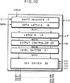
図10は、データ走査信号を生成するためのXドライバのブロック図である。
図11は、Yドライバの各部の動作を説明するためのタイミングチャートである。
図12は、Xドライバの各部の動作を説明するためのタイミングチャートである。
図13は、本発明の電源回路の一例を示す回路図である。
図14は、本発明の他の電源回路の一例を示す回路図である。
図15は、本発明のさらに他の電源回路の一例を示す回路図である。
図16は、カイラルネマチック液晶の閾値、飽和値と温度との関係を示す特性図である。
図17は、カイラルネマチック液晶の閾値、飽和値と反転時間mHとの関係の実験結果を示す特性図である。
図18は、カイラルネマチック液晶の閾値、飽和値と反転時間mHとの関係の他の実験結果を示す特性図である。
図19は、図18のデータに基づいて作成された、飽和値−閾値と反転時間mHとの関係を示す特性図である。
図20は、カイラルネマチック液晶の閾値、飽和値と反転時間mHとの関係の他の実験結果を示す特性図である。
図21は、図20のデータに基づいて作成された、飽和値−閾値と反転時間mHとの関係を示す特性図である。
図22は、カイラルネマチック液晶を駆動するための選択電圧に関する閾値を示す特性図である。
図23は、7レベル駆動法を示す波形図である。
図24は、図9に示すYドライバの出力電圧を決定するための真理値表である。
図25は、図10に示すXドライバの出力電圧を決定するための真理値表である。
発明を実施するための最良の形態
次に、図面を参照して本発明の実施例を説明する。
液晶セルの構造
後述する各実施例に用いた液晶材料は、ネマチック液晶(例えば、E.Merck社製ZLI−3329)に光学活性剤(例えば、E.Merck社製S−811)を添加することにより、液晶のヘリカルピッチを3〜4μmに調整したものである。図1に示すように、上下のガラス基板5,5上にITOからなる透明電極4のパターンを形成し、その上に各々ポリイミド配向膜(例えば、東レ社製SP−740)2を塗布した。そして、各ポリイミド配向膜2対して、相互に所定角度φ(実施例ではφ=180゜)異なる方向にラビング処理を施して、セルを構成した。上下のガラス基板5,5の間にはスペーサを挿入して基板間隔を均一化し、例えば基板間隔(セル間隔)を2μm以下とした。したがって、液晶層厚/ねじれピッチの比は0.5±0.2となる。
このセルに液晶を注入すると、液晶分子1のプレチルト角θ1,θ2は数度となり、初期配向が180゜のツイスト状態となる。この液晶セルを、図1に示す偏光方向の異なる2枚の偏光板7,7で挟み込み、表示体を形成した。なお、3は絶縁層、6は平坦化層、8は画素間の遮光層、9は液晶分子1のダイレクターベクトルである。
液晶駆動原理
図2は、液晶に印加される電圧の極性反転を周期的に行い、液晶を交流駆動する際の駆動波形の一例を示している。反転のタイミングは、後述する走査信号の選択期間T3を1Hとしたとき、そのm倍(mは2以上の整数)のmHごとである。ただし、mH≠1フレーム期間である。このmHのパルス幅の信号を、図2(a)にFRとして示した。図2(b)はi番目の走査信号ラインに供給される走査信号の波形を示している。図2(c)はj番目のデータ信号ラインに供給されるデータ信号の波形を示している。図2(d)は図2(b)の走査信号と図2(c)のデータ信号との差信号の波形を示している。図2(d)の差信号の電圧が、i番目の走査信号ラインとj番目のデータ信号ラインとの交差点に位置する画素(i,j)の液晶に印加される。
図2に示す駆動波形には、リセット期間T1,遅延期間T2,選択期間T3および非選択期間T4が含まれている。この各期間T1,T2,T3,T4を加算した期間が1フレーム期間Tである。
図2において、リセット期間T1には、ネマチック液晶にフレデリクス転移を生じさせるための閾値以上のリセット電圧(リセットパルス)100が印加される。このリセット電圧100は、本実施例ではそのピーク値が例えば±25Vに設定されている。遅延期間T2は、リセット電圧100を液晶セルに印加した後、選択期間T3にて液晶セルに選択電圧(選択パルス)120が印加されるタイミングを遅延させるために設けられている。本実施例では、この遅延期間T2にて液晶セルに、遅延電圧110として例えば±1Vの電圧が印加される。選択期間T3に液晶セルに印加される選択電圧120は、ネマチック液晶の2つの準安定状態、例えば360゜ツイスト配向状態と0゜ユニフォーム配向状態のいずれかを生ずる臨界値を基準として選択される電圧である。この選択電圧120として、第1実施例に用いたカイラルネマチック液晶の場合、選択電圧120のピーク値が0〜±1.5Vのoff電圧であると、360゜ツイスト配向状態が得られる。一方、選択電圧120として2V以上又は−2V以下、望ましくは3V以上又は−3V以下のon電圧を液晶セルに印加すると、0゜ユニフォーム配向状態が得られた。また、非選択期間T4には、液晶セルに選択電圧120よりも絶対値の小さな非選択電圧130が印加され、選択期間T3にて選択された液晶の状態が維持されるようになっている。
図3は、カイラルネマチック液晶の各種状態を説明するための説明図である。
この液晶は、初期配向状態にあっては、上述のラビング処理により180゜ツイスト配向状態となっている。この初期配向状態の液晶に、リセット期間T1にてリセット電圧100を印加すると、図3に示す通りフレデリクス転移が生ずる。この後に、選択期間T3にて選択電圧120としてon電圧を液晶に印加すると0゜ユニフォーム配向状態が得られ、off電圧を印加すると360゜ツイスト配向状態が得られる。その後、図3に示すように、ある時定数に従って上記の2つのいずれかの状態から初期状態に自然緩和する。ここで、この時定数は表示に必要な時間に比較して十分長くできる。従って、非選択期間T4にて印加される非選択電圧130が、フレデリクス転移を起こすために必要な電圧に比べて十分に低い電圧に保たれている限り、次のリセット期間T1までの間は、選択期間T3にて設定された状態をほぼ維持できる。これにより、液晶表示が可能となる。
遅延時間T3を設けている理由について、図4を参照して説明する。図4は、本発明で用いる双安定液晶の挙動を示した動的シミュレーションの結果と、遅延期間T2および選択期間T3との関係を示している。横軸は時間、縦軸は液晶セル中央の分子のティルトを表しており、スタート時点はリセットパルス100の切れた時である。
この図に従えば、液晶分子は垂直に立った状態(ホメオロトロピックの配向状態)の後、後ろ側に少し倒れ(バックフロー)、再び戻って来てティルトが0゜に向かって進むものと、更に180゜の方向に動くものに分かれる。前者は0゜ユニフォーム配向状態への遷移であり、後者はこのティルトの変化の他にツイストも加わるので360゜ツイスト配向状態への遷移に相当する。ところで、この図で明らかなように0゜ユニフォーム配向状態への遷移にしても、360゜ツイスト配向状態への遷移にしても、リセットパルス100の切れた直後は、液晶のバックフローという同一の過程を経ている点では全く挙動が同じである。すなわち、液晶の配向状態が0゜になるか360゜になるかは、このバックフロー後のトリガー(図4中の矢印)の与え方次第で決まる。
本願出願人の先の提案では、リセット期間T1の経過直後に選択期間T3を設定した。これに対して、第1実施例の駆動方法に係る図2の駆動方法では、リセット期間T1と選択期間T3との間に遅延期間T2を挿入した。この遅延期間T2の時間長さを調整することで、選択期間T3の長短にかかわらず、液晶がバックフローを起こした後のトリガーを付与すべきタイミングにて、この液晶に選択電圧32を印加することが可能となる。それゆえ、選択期間T3の時間長さを50μsと大幅に短縮しても、液晶のon/offの切り換えが可能となる。
選択パルスのパルス幅、遅延期間及び温度を一定にした場合、臨界値は選択パルスのパルス高として図22に示すVth1,Vth2のようになる。図22に示すリセットパルスの電圧値Veの絶対値(縦軸)と選択パルスの電圧値Vw(横軸)との直交平面において、a1,a2は準安定状態の一方(例えばねじれ角0度の状態)が出現する領域(|Ve|>V0かつ|Vth1|<|Vw|<|Vth2|)を示している。また、b1,b2,b3は準安定状態の他方(例えばねじれ角360度の状態)が出現する領域(|Ve|>V0かつ|Vw|<|Vth1|又は、||Ve|>V0かつ|Vw|>|Vth2|)を示す。ここでVth1とVth2は選択パルスの電圧値に対する閾値である。以下の説明では、Vth1を閾値として液晶駆動を行っている。
図2の駆動波形の説明
次に、図2に示す駆動波形の詳細について説明する。この第1実施例では、計8レベルの電圧レベルを用いてカイラル・ネマチック液晶を駆動している。
この8レベルの電圧レベルを、低電圧側の第1群の4レベル(V1、V2、V3、V4:V1<V2<V3<V4)と高電圧側の第2群の4レベル(V5、V6、V7、V8:V4<V5<V6<V7<V8)とで構成している。
さらに、本実施例では、mH(図2ではm=4)ごとに、走査信号及びデータ信号はそれぞれ、第1群又は第2群の電圧レベルに交互に設定される。
走査信号のリセット期間T1は、数10H分(例えば1〜2ms)の時間に設定される。このリセット期間T1は反転時間mHより長いため、リセット期間T1中では、mHごとに電圧レベルが変化する。図2では、走査信号のリセット期間T1では、V1またはV8の電圧レベルが交互に繰り返される波形となる。
次に、走査信号の遅延期間T2は1H以上とされ、図2の場合にはT2=2Hに設定される。T2<mHであるから、走査信号の遅延期間T2では一定電圧レベルとなるが、mHごとの反転に従って異なる電圧レベルとなり、本実施例ではV3又はV6のいずれかの電圧レベルとなる。ここで、本実施例では、リセット期間T1の最後のパルス幅が2Hであり、この最後のパルス期間とは位相の異なる遅延期間T2も2Hとなっている。そこで、リセット期間T1と比較して、選択期間T3以降は、走査信号波形のmHごとの反転位相を180゜変化させている。
選択期間T3=1H<mHであり、選択期間T3では一定電圧となるが、mHごとの反転に従って異なる電圧レベルとなり、本実施例ではV1とV8のいずれかの電圧レベルとなる。
非選択期間T4>mHであり、1フレーム期間内でmHごとに異なる電圧レベルとなる。本実施例では、走査信号の非選択期間T4では、V3、V6の電圧レベルを持つ波形となる。
一方、データ信号もmHごとに電圧レベルが変化する波形となり、しかも液晶に書き込む電圧に依存してon電圧又はoff電圧となる。on電圧は、走査信号の選択期間T3の電圧がV1である時はV4、V8である時はV5となる。off電圧は、走査信号の選択期間T3の電圧がV1である時はV2、V8である時はV7とされる。
このような走査信号、データ信号をそれぞれ走査信号ライン、データ信号ラインに供給すると、各ラインの交点である画素(i、j)には、図2(d)に示す差信号の電圧が印加される。すなわち、リセット期間T1ではリセット電圧130として、比較的大きな電圧(V1−V7)あるいは(V8−V2)が得られる。しかも、従来の電圧平均化法と同じon電圧、off電圧、バイアス電圧の関係が得られる。
特に、V4−V3=V3−V2=V7−V6=V6−V5とすれば、非選択期間T4のバイアス電圧が等しくかかるように設定できる。この条件下でon電圧を大きくしたい時には、V1、V2間とV7、V8間の電圧差を大きくすれば良い。ただし、この時同時に非選択期間T4中のバイアス電圧も増加するので注意を要する。また、リセット電圧を大きくしたい時には、V4、V5間の電位差をさらに広げれば良い。さらには、これにリセット電圧印加後の遅延期間の長短をつけるには、選択期間のタイミングを1H単位でシフトさせればよい。
ちなみに、V1=0V、V2=1V、V3=2V、V4=3Vの第1群と、V5=23V、V6=24V、V7=25V、V8=26Vの第2群、または、V1=−13V、V2=−12V、V3=−11V、V4=−10Vのマイナス電圧第1群と、V5=10V、V6=11V、V7=12V、V8=13Vのプラス電圧第2群に各々の電圧を設定すると、リセット電圧=±25V、ON電圧=±3V、OFF電圧=±1V、バイアス電圧=±1Vが得られる。第1群の電圧V4と第2群の電圧V5間の電位差をさらに広げるように設定すれば、30V、40Vのリセット電圧とバイアス電圧1Vということも実現できる。
このように、図2の駆動法によれば、カイラルネマチック液晶の駆動に必要な大電圧と小電圧を同居させ、単純マトリクス駆動を合理的に実現できる。即ち、図2の駆動法を用いれば、比較的小さな回路電圧で20Vを越える大きなリセット電圧と、1V近辺のバイアス電圧(非選択電圧)と、数Vのデータon,off電圧を両立させ、しかも液晶に印加される電圧を最適反転時間で交流化する事ができる。また、実際の駆動回路を作製する上では、データ信号と走査信号とで、それぞれの駆動電圧が接近するので、回路部品の選択の自由度が広がる。さらには、この様な駆動電圧のアンバランスの解消は、駆動回路のIC化にも有効となる。
なお、上記説明ではリセット電圧の組を(V1、V8)としたが、(V2、V7)あるいは(V3、V6)あるいは(V4、V5)としてもよい。リセット電圧の組を(V4,V5)とした例は、図6を用いて後述する。また、図2の駆動法は、遅延期間T2がない場合にも有効である。
mH反転と表示特性との関係
図2の駆動法にて採用したmHごとの交流駆動は、単に液晶の長寿命化に寄与するだけでなく、カイラルネマチック液晶を用いた液晶表示装置での表示特性をも向上させることができる。その理由について以下に説明する。
図16は、カイラルネマチック液晶の閾値Vth、飽和電圧Vsatと温度との負の相関を示す特性図であり、閾値Vth、飽和電圧Vsatは温度依存性を有する。ここで、Vsを選択期間T3中の走査信号の電圧レベルの絶対値とし、Vdを選択期間T3中のデータ信号の電圧レベルの絶対値とすると、液晶のオン・オフ駆動の条件は、|Von|=|Vs+Vd|≧|Vsat|、かつ、|Voff|=|Vs−Vd|≦|Vth|である。設計上、Vonの絶対値はVsatの絶対値よりもあるマージンを越えて大きく設定し、Voffの絶対値はVthの絶対値よりもあるマージンを下回る値に設定する必要があるが、温度に依存してマージンが少なくなり、表示特性が悪化する恐れがある。
また、この閾値Vth、飽和電圧Vsatは、液晶パネルの面内にてばらつくことも分かっている。
ところで、飽和電圧と閾値電圧との差の絶対値|Vsat−Vth|が小さければ、閾電圧、飽和電圧に温度依存性があっても、あるいは面内での非均一性があっても、on電圧、off電圧のためのマージンを常に確保することが可能となる。
本発明者等は、|Vsat−Vth|が反転時間mHに依存して変化することを発見した。図17は、横軸に反転時間mHをとり、縦軸に閾値Vth、飽和電圧Vsatをとり、実験により得られた閾値Vth、飽和電圧VsatのmH依存特性を示すものである。なお、この実験は、デューティー比=1/240、リセット期間T1=1.5mS、リセット電圧=±25V、バイアス電圧Vd=±1Vとして常温下で測定したものである。
図18〜図21の特性図によれば、|Vsat−Vth|が反転時間mHに依存することをより明確に理解できる。
図18は、図17と同じ実験をmHを1H〜8H(1H=80μS)に変化させて行ったものである。実験条件は、デューティー比=1/240、リセット期間T1=1.0mS、リセット電圧=±25V、バイアス電圧Vd=±1.3Vとし、常温下で測定したものである。図18によれば、Vth1、飽和電圧Vsat1は、2H〜4Hの間で低くなることが分かる。
図19は、図18のデータに基づき、縦軸を|Vsat−Vth|とした特性図であり、2H〜4Hの間で|Vsat−Vth|が低下していることが分かる。
図20は、図19と同じ実験を、デューティー比=1/480の液晶パネルにて実施した結果を示している。1H=40μSである。図20によれば、Vth1、飽和電圧Vsat1は、4H〜16Hの間で低くなることが分かる。
図21は、図20のデータに基づき、縦軸を|Vsat−Vth|とした特性図であり、4H〜16Hの間で|Vsat−Vth|が低下していることが分かる。
このように、mHを2H以上とすると、mH=1Hの場合と比較すれば、|Vsat−Vth|を小さくでき、マージンを大きく確保した状態でon電圧、off電圧を液晶に印加することができ、表示特性が向上することが分かる。
しかも、mHを2H以上とすると、mH=1Hの場合と比較すれば閾値Vth、飽和電圧Vsat自体を低くでき、駆動電圧を低くできる効果もある。
このように、図2の駆動方法によれば、反転時間mHと表示特性の依存性が確認されているので、反転動作によって液晶の寿命と関係の深い直流の連続印加を極力抑えると同時に、表示特性の改善も出来る。
図5の駆動波形の説明
図5は図2と同じように、mH(m=4)のパルス幅のFR(図5(a)参照)を用い、液晶に印加される電圧極性をmHごとに反転させる方法であるが、走査信号とデータ信号の波形の各電圧レベルを変更してある。
走査信号は、図5(b)に示すように、リセット期間T1の電圧はV4、V5、遅延期間T2の電圧はV2、V7、選択期間T3の電圧はV4、V5、非選択期間T4の電圧はV2、V7としている。
データ信号は、図5(c)に示すように、on電圧をV1、V8、off電圧をV3、V6としている。
この結果、マトリクス表示の画素(i,j)には、図5(d)に示すように、液晶に印加される電圧が、プラス・マイナスに交互に変化したものとなる。この図5の駆動波形を用いると、V1〜V8を図2の電圧レベルと同じに設定した場合には、リセット電圧は(V4−V8)又は(V5−V1)となり、±23Vとなって図2の場合より低くなるが、リセットに必要な大きな電圧を確保できる。他の電圧は、ON電圧=±3V、OFF電圧=±1V、バイアス電圧=±1Vとなり、図2と同じ電圧が得られる。さらには、データ信号の電位を、グランド電圧V1と最高電圧V8に設定できるので、バイアス電圧が安定し、表示の安定性を増す事ができる。
なお、図5の場合には、V3−V2=V2−V1=V8−V7=V7−V6とすれば、非選択期間T4のバイアス電圧が等しくかかるように設定できる。また、図2と同様に、on電圧を大きくしたい時には、V1、V2間とV7、V8間の電圧差をそれぞれ大きくすれば良い。リセット電圧を大きくしたい時には、V4、V5間の電位差をさらに広げれば良い。さらには、これにリセット電圧印加後の遅延期間の長短をつけるには、選択期間のタイミングを1H単位でシフトさせればよい。
図6の駆動波形の説明
図6は、図2、図5と同じmH(m=4)ごとの反転動作に、フレーム単位の反転動作を重ねた変形例である。
即ち、走査信号及びデータ信号の電圧レベルをmHごとに反転させていくと、1フレームが終わる段階では、液晶にかかる電圧が1フレーム内ではプラス・マイナスのバランスが取れていないので、直流分が残留する。そこで、次のフレームでは、走査信号、データ信号の電圧レベルを前フレームと反転させ、フレーム単位で反転させている。即ち、液晶に印加される駆動波形の第nフレーム(nは整数)の始まりの電圧が、電圧レベルの第1群(V1〜V4)にある時は、第(n+1)フレームの始まりは第2群(V5〜V8)とする。また、第nフレームの始まりの電圧が第2群の時は、第(n+1)フレームの始まりは第1群とし、mHごとの反転にフレーム単位の反転を重ねて繰り返すようにする。これはフレームごと反転とmHパルス反転を組み合わせたものといえる。
この図6の駆動波形によれば、1フレーム内では解消できない直流分を、2フレームに渡って完全解消できるので、液晶の長寿命化に効果が大である。
なお、本実施例は図2の実施例と同一電圧設定としたが、図5の実施例2と同一電圧設定としてもよい。図5の駆動法にフレーム反転を付加した駆動波形は、図7に示す通りとなる。
液晶駆動回路の説明
図8から12に、図2、5、6、7の駆動波形を実現するための実際の液晶駆動回路の構成、並びにタイムチャートを示す。図8は液晶パネルおよびその駆動回路を含む表示装置の全体構成図である。液晶パネル10は320×320画素を有し、この液晶パネル10を駆動するために、第1、第2のYドライバ回路11A、11Bおよび第1、第2のXドライバ12A、12Bが設けられている。
第1、第2のYドライバ回路はそれぞれ同一の構成を有し、その詳細が図9に示されている。
Yドライバ回路11Aについて図9を参照して説明する。Yドライバ回路11Aは、リセット用シフトレジスタ13A、セレクト用シフトレジスタ13Bの2つのシフトレジスタを有し、それぞれには160段のレジスタがある。リセット用レジスタ13Aにはリセット期間T1を指定したリセット信号RIが入力され、この信号はシフトクロックYSCKにより次段のレジスタに逐次シフトされていく。なお、160段目のレジスタの内容は出力端子ROを介して出力され、第2のYドライバ回路の入力RIとなるカスケード接続がなされる。セレクト用シフトレジスタ13Bについても同様で、セレクト期間T3を指定した信号SIがシフトレジスタ13Bに入力され、これらの信号はシフトクロックYSCKにより次段のレジスタに次々に伝達されていく。最終段160のレジスタの内容は出力端子SOを介して次の第2のYドライバ回路11Bの入力信号SIとなり、カスケード接続がなされる。
各シフトレジスタ13A、13Bの内容は160チャネル同時に並列出力され、出力コントローラ14に入力される。この出力コントローラ14はリセット信号R、セレクト信号Sおよび交流化信号FRの入力状態によって6つの状態、即ち、R,S、FR=(0、0、0)または(0、0、1)または(0、1、0)または(0、1、1)または(1、0、0)または(1、0、1)を区別した信号を出力する。この信号は、レベルシフタ15を介してYドライバ16に入力される。
このYドライバ16には4種類の駆動電圧(V1,V3,V6,V8)または(V2,V4,V5,V7)が入力されており、出力コントローラ14で区別された6つの状態に基づき、図24を示す真理値表に従っていずれか1つの駆動電圧を各チャネルごとに出力する。なお、図24において、Yout1は、図2、6に対応した駆動波形を得るときの選択を、また、Yout2は図5、7に対応した駆動波形を得るときの選択を示した。
図11はYドライブ回路に入出力される各信号の状態を一部示したタイミングチャートである。図11に示すタイミングチャートの場合、選択期間T3の長さを1Hとしたとき、シフトクロックYSCKは1HごとにH/Lを繰り返す信号となっており、交流化信号FRはmHとなているので、図2、5のようにmHごとに液晶に印加される電圧の極性が反転する走査信号YKとなる。
次に、第1のXドライバ回路12Aの詳細について図10を参照して説明する。Xドライバ回路12Aは、160段のレジスタから構成されるシフトレジスタ17有し、入力信号EIをシフトクロックXSCKに従って次段のレジスタに逐次シフトしていく。160番目のレジスタの内容はEO出力端を介して外部に出され、第2のXドライバ回路12Bとカスケード継続が可能である。シフトレジスタ17に入力される信号EIは、図12に示すように一水平走査期間(1H)に1回論理の1となる信号である。従って、シフトレジスタ17の各レジスタより論理の1が逐次出力されることで、第1のラッチ回路18は各レジスタと対応するアドレスに画像データをラッチする事になる。この第1のラッチ回路18の160チャンネルのデータは、ラッチパルスLPが入力するタイミングにて第2のラッチ回路19に同時にラッチされる。交流化信号FRおよび第2のラッチ回路19からのデータを入力する出力コントロール回路20は、データDと交流化信号FRの入力状態によって4つの状態(D,FR)=(0、0)または(0、1)または(1、0)または(1、1)を区別した信号を、レベルシフタ21を介在して各チャンネルごとにXドライバ22に入力させる。Xドライバ22は4種類の駆動電圧すなわち(V2,V4,V5,V7)または(V1,V3,V6,V8)を入力とし、出力コントロール回路20からの情報に基づいてこの内の1つの電圧を選別出力する。図25にその真理値表を示す。なお、図25においてXOUT1は図2、6に、XOUT2は図5、7の実施例に対応している。
電源回路の説明
図8から図12に示した回路で使用する電源回路の実施例について説明する。本発明では走査信号、データ信号の各種電圧レベルを設定するために、計8レベルの電位を用いている。このうちV1=GND、V8=最大基準駆動電圧(VH)とすると、残りの中間のV2〜V7について各々の電位を決めれば良い事になる。以下に説明する各電源回路は、多数の電圧レベルに分かれた駆動電位を、1つのボリュームによって全て同時に可変とする事ができ、表示の最適調整には最も簡便な電源回路である。
まず、電圧平均法で非選択期間中のバイアス電圧となる基準電位差VBを、データ信号のVon、Voffより次のように定義し、一定となるようにする。
VB=|Von−Voff|/2
この基準電位差VBを基準に電源回路を実現したものが図13である。
VBは数Vあれば充分であるので、例えば高電圧のVHからツェナーダイオード30によって電位を落とし、更に、この電位からバリアブル抵抗32の中点の電位を任意に引き出し、基準電位差VBとする。必要な電圧V2、V3、V4は、このVBを1〜数倍に増幅したものをV1に加えればよいので、図13のように正の増幅回路をオペアンプにより構成し、V1=0V(グランド)であることを考慮すると、V2=VB、V3=2VB,V4=aVB(aは増幅率)とする。増幅率aは、V4の電圧を出力するオペアンプのフィードバック抵抗34により決定され、この抵抗値を可変とすれば、増幅率aを任意に設定できる。
次に、これらの出力と最高電位VHの引き算回路をオペアンプにより構成し、V7=VH−V2、V6=VH−V3、V5=VH−V4とすれば、VBを変えるだけで全電圧レベルが連動して変わるバイアス一定の電源となる。実際には、走査信号およびデータ信号のドライバー回路に入力させる前に、バッファを介在させれば、このバッファにより各電圧レベルを増幅できる。
本電源回路は、増幅率aを変更することでV4、V5を最適に調整でき、図5、図7の実施例のon電圧(V1−V4またはV8−V5)を所望に調整できる。なお、増幅の倍率を(a−2)、(a−1)、aとなるようにV2、V3、V4を決めると、図2、6の実施例に好適となる。
図14は、V3=bVB、V2=(b−1)VB、V4=(b+1)VBとなるようにオペアンプにより演算回路を組み、V2〜V4の電位を作成したものである。ただし、bは増幅率であり、bは1以上の数値、さらに好ましくは2以上の数値である。V5〜V7については図13と同様に、VH(V8)からそれぞれV4、V3、V2を、オペアンプにより構成した減算回路によって減算して作成している。ここで、図14では、V3の電圧を出力するオペアンプのフィードバック抵抗34を可変抵抗とし、増幅率bの値を自由に変えられるようにしている。この結果、V4、V5の各電圧レベルを調整できる。従って、図2、図6の実施例のon電圧(V1−V4またはV8−V5)を所望に調整できる。このように、液晶に印加されるon電圧を簡単に操作する事ができ、これも駆動回路調整に有効となる。
図15は、本発明のさらに他の電源回路を示している。同図において、7個の抵抗器(R1、R2…R7)が設けられ、このラインの一端には最大電圧レベルV8を生成する電圧発生回路40が接続され、他端がグランド電圧レベルV1となっている。そして、隣接する2つの抵抗器の間には、抵抗器(R1、R2…R7)にて順次電圧降下されて得られる電圧レベルV7〜V2を出力する6個の電圧出力端子0UT7〜OUT2が設けられている。V5の電圧出力端子OUT5と、V4の電圧出力端子0OT4との間の抵抗器R4は可変抵抗器であり、その抵抗値を外部より変更することができる。
この電源回路では、抵抗器R4の抵抗値の変更によって、各抵抗器R1〜R7を流れる電流値を変更でき、降下電圧の大きさを変更できるので、グランド電圧レベルV1と最大電圧レベルV8を除く各電圧レベル(V2〜V7)を同時に調整可能となる。なお、電圧発生回路40にてV8の大きさも変更すれば、V2〜V8を任意に変更することが可能となる。なお、図14、図15において、V2〜V7の電圧レベルが出力されるOUT2〜OUT7には、それぞれ増幅用のオペアンプが接続されることもある。
なお、本発明は上記実施例に限定されるものではなく、本発明の要旨の範囲内で種々の変形実施が可能である。例えば、図2、図6に示す実施例では、反転時間を決定する値mと、ディスプレイの走査ライン数nの間に最大公約数が無い様に設定すると反転位置が自然にずれていき、反転による波形なまりやクロストークを目立たなくする事が可能である。また、mを適当に大きくすれば、電圧反転で発生するクロストーク位置が少なくなる効果もある。Technical field
The present invention relates to a bistable liquid crystal display device having a memory property using a chiral nematic liquid crystal, a driving method thereof, and a driving circuit used therefor. The present invention further relates to a liquid crystal display device for setting a total of eight or more voltage levels optimal for driving a chiral nematic liquid crystal, and a power supply circuit device used therefor.
Background art
A bistable liquid crystal display using a chiral nematic liquid crystal is already disclosed in Japanese Patent Publication No. 1-51818, and describes initial alignment conditions, two stable states, and a method of realizing the stable state.
However, the contents described in Japanese Patent Publication No. 1-51818 only describe operations or phenomena in two stable states, and do not suggest means for putting them into practical use as a display. Further, the above-mentioned publication does not describe anything about a matrix display having the highest practical application and the highest display capability as a display body at present, and does not disclose any driving method.
Therefore, in Japanese Patent Application Laid-Open No. Hei 6-230751, we have proposed a method of controlling the back flow generated in the liquid crystal cell and improving the above-mentioned disadvantage. In this method, a high voltage of about 1 ms is first applied to cause a Freedericksz transition, and then a 0 ° uniform state is created by a constant voltage pulse having a polarity opposite to or the same as or higher than the pulse immediately following the pulse. Similarly, a pulse period shorter than the threshold immediately following the Freedericksz transition voltage is provided to realize a 360 ° twist state. In this method, the writing time per line of the matrix display is set to 400 μs, and the writing of 400 lines or more requires a total of 160 ms (6.25 Hz) or more. Had a problem.
Therefore, the present inventors have further filed Japanese Patent Application No. 5-37057 as means for improving the writing time. As shown in FIG. 2 or FIG. 4 of this application, a delay time is provided after a reset pulse causing Freedericks transition, and thereafter, an ON or OFF selection signal is applied. In this way, the writing time was several times faster than in the past, for example, 50 μs.
However, in these driving methods, a large reset voltage exceeding 20 V, an off voltage of 1 to 3 V for obtaining two stable states of display, and a selection voltage of about 6 to 7 V from the on voltage of several V are efficiently achieved on a circuit. In addition, it is necessary to make an alternating current to extend the life of the liquid crystal.
FIG. 23 shows a seven-level driving method in which a driving waveform of a bistable display is created following the voltage averaging method. FIG. 23A shows the waveform of the scanning signal, in which Vr exceeding 20 V is applied to the reset period T1, the selection period T3 after the delay period T2 is ± Vs, and the remaining non-selection period T4 is zero potential. . On the other hand, the data signal is turned on / off by giving an in-phase or out-of-phase AC pulse to the selection pulse having the amplitude ± Vd shown in FIG. Then, the voltage of the difference signal between the scanning signal and the data signal as shown in FIG. 23C is applied to the liquid crystal.
Here, since the bias voltage Vd is sufficient at around 1 V, a large voltage difference occurs between the scanning signal waveform and the data signal waveform. Particularly, in the scanning signal waveform, a voltage difference of about 20 V is generated between Vr and Vs, which is not desirable in terms of the circuit structure.
As described above, in the bistable liquid crystal display, the ratio between the scanning voltage and the on / off signal voltage at the time of matrix driving is largely unbalanced. Therefore, in forming a specific driving circuit, this circuit is integrated into an IC. Above, this imbalance has the potential to be a major obstacle.
On the other hand, although the voltage averaging drive method of the conventional matrix type liquid crystal display is not so extreme, a 6-level method has been devised from the same situation (Liquid Crystal Device Handbook, Nikkan Kogyo, p401). However, this is effective in balancing the driving voltages of the scanning waveform and the signal waveform, and in increasing the ratio between the on-voltage and the bias voltage, but it is also effective in resetting with a large voltage difference as in the present invention. When a voltage is applied, the present invention cannot be applied to driving of the chiral nematic liquid crystal as it is.
Further, in the above method, since the number of levels of the driving voltage is large, adjustment of the optimum driving voltage is very complicated, and a practical problem has arisen.
Further, it has been found that the threshold voltage and the saturation voltage of the bistable liquid crystal have a temperature dependency and vary within the liquid crystal panel surface, so that there is a problem that it is difficult to secure stable display characteristics.
Therefore, an object of the present invention is to provide a liquid crystal display device capable of improving display characteristics without generating a large voltage difference between a scanning signal waveform and a data signal waveform, a driving method thereof, and a driving circuit using the same. It is in.
Another object of the present invention is to provide a liquid crystal display device and a power supply circuit device for the same, which can accurately generate a large number of voltage levels of eight or more levels and can easily adjust the multiple levels with a simple operation. It is in.
Disclosure of the invention
The present invention provides a liquid crystal display device which applies a voltage of a difference between a scanning signal having at least a reset period, a selection period, and a non-selection period and a data signal in one frame to a chiral nematic liquid crystal having at least two stable states. In the driving method of
Prepare a total of eight or more voltage levels, including a plurality of levels of a first group on a low voltage side and a plurality of levels of a second group on a high voltage side,
The voltage level of the scanning signal and the data signal is changed every integer time mH (m is an integer of 2 or more and mH ≠ 1 frame period) of a unit time (1H) corresponding to the selection period of the scanning signal. Respectively, alternately changing between the first group and the second group,
When the data signal is at the voltage level of the first group, the voltage level of the reset period in the scan signal is selected from the second group, and the data signal is at the voltage level of the second group. When, the voltage level of the reset period in the scanning signal is selected from the first group,
When the data signal is at the voltage level of the first group, the voltage levels of the selection period and the non-selection period in the scanning signal are respectively selected from the same first group, and the data signal is at the first group. When the voltage levels are of two groups, the voltage levels of the selection period and the non-selection period in the scanning signal are respectively selected from the same second group,
The polarity of the voltage applied to the liquid crystal is inverted every mH.
The liquid crystal display device according to the device of the present invention,
A liquid crystal panel in which at least two stable chiral nematic liquid crystals are sealed between a first substrate on which a plurality of scanning electrodes are formed and a second substrate on which a plurality of data electrodes are formed; ,
A scan electrode driving circuit that outputs a scan signal having at least a reset period, a selection period, and a non-selection period in one frame to each of the scan electrodes;
A data electrode drive circuit that outputs a data signal to each of the data electrodes;
A power supply circuit for outputting a total of eight or more voltage levels as a potential of the scan signal and the data signal, the power supply circuit comprising a plurality of levels of a first group on a low voltage side and a plurality of levels of a second group on a high voltage side;
Having. The scan electrode drive circuit and the data electrode drive circuit set various voltage levels for carrying out the method of the present invention.
In the drive circuit of the liquid crystal display device according to the present invention, the scan electrode drive circuit and the data electrode drive circuit for setting various voltage levels for implementing the method of the present invention are defined. This drive circuit can be formed not only on a liquid crystal display substrate but also as an external circuit to a liquid crystal panel.
According to the above-described present invention, by selecting the voltage level from the first group on the low voltage side and the second group on the high voltage side as described above, a large difference between the voltage amplitude of the scanning signal and the voltage amplitude of the data signal is obtained. Without causing a difference, it is possible to apply a reset voltage having a large absolute value exceeding, for example, 20 V, and a non-selection voltage, for example, around 1 V, to the liquid crystal as the voltage of the difference signal. This is advantageous in forming the drive circuit, particularly in making the drive circuit into an IC.
The reason for inverting the polarity of the voltage applied to the liquid crystal every mH is as follows. The present inventors have discovered that the voltage difference between the saturation voltage Vsat of the chiral nematic liquid crystal and the threshold voltage Vth changes depending on the value m that determines the inversion time (see FIGS. 17 to 21). As disclosed in the prior application of the applicant of the present application (Japanese Patent Application No. 5-352493), when the inversion every 1H is adopted, in other words, compared with the case where m = 1 is adopted, the present invention provides the above-mentioned voltage difference. Can be selected from the region in which is reduced to determine the inversion time.
Incidentally, the absolute value of the on-voltage applied to the chiral nematic liquid crystal during the selection period needs to be set to be larger than the absolute value of the saturation voltage Vsat of the chiral nematic liquid crystal. On the other hand, the absolute value of the off voltage applied to the chiral nematic liquid crystal during the selection period needs to be set smaller than the absolute value of the threshold voltage Vth of the chiral nematic liquid crystal. Here, the saturation voltage and the threshold voltage change depending on environmental conditions such as the ambient temperature (see FIG. 16). Alternatively, when the saturation voltage and the threshold voltage of the liquid crystal of each pixel in the liquid crystal panel are compared, they are not uniform in the liquid crystal panel surface. Therefore, the voltage difference between the saturation voltage Vsat and the threshold voltage Vth of the chiral nematic liquid crystal also changes depending on environmental conditions or is non-uniform in the liquid crystal panel, and in the worst case depending on the setting of the on voltage and the off voltage. , On, off does not occur. If the absolute value of the voltage difference between the saturation voltage Vsat and the threshold voltage Vt of the chiral nematic liquid crystal can be reduced, the allowable margin of the on / off voltage can be relatively increased. As a result, the adverse effect of the voltage difference depending on the environmental conditions or the position in the liquid crystal panel can be reduced, and the display characteristics can be improved.
In other words, by reducing the absolute value of the voltage difference between the saturation voltage Vsat of the chiral nematic liquid crystal and the threshold voltage Vth, the absolute value of the on-voltage applied to all the pixels of the chiral nematic liquid crystal becomes chiral The absolute value of the saturation voltage Vsat of the nematic liquid crystal can be set larger than the absolute value of the allowable margin, and the absolute value of the off voltage applied to all the pixels of the chiral nematic liquid crystal is the threshold voltage of the chiral nematic liquid crystal. It can be set smaller than the absolute value of Vth below the allowable margin.
In the above driving method, it is preferable that a delay period is provided between the reset period and the selection period. In this case, the voltage level of the scanning signal during the delay period is set to be the same as the voltage level during the non-selection period.
This makes it possible to shorten the selection period in the scanning signal, that is, the writing time.
The above driving method is suitable for driving a chiral nematic liquid crystal using a total of eight voltage levels. Driving this chiral nematic liquid crystal requires a total of 10 voltage levels described below.
First, the data signal needs to be set to a data voltage level including either the ON voltage level or the OFF voltage level for each selection period. As the data voltage level of the data signal, it is necessary to set four types of voltage levels for applying a positive and negative ON selection voltage and a positive and negative OFF selection voltage to the liquid crystal, respectively.
Next, the scanning signal needs to be set to the reset voltage level during the reset period, set to the selection voltage level during the selection period, and set to the non-selection voltage level during the non-selection period. As the reset voltage level, two voltage levels for applying a positive and a negative reset voltage to the liquid crystal during the reset period, respectively, are required. As the selection voltage level, two voltage levels for applying a positive and a negative selection voltage to the liquid crystal during the selection period are required. As the non-selection voltage level, two types of voltage levels for applying a bias voltage level during the non-selection period are required.
As described above, a total of at least 10 levels are required, but by sharing two reset voltage levels and two selection voltage levels, the chiral nematic liquid crystal is driven using a total of eight levels. be able to.
The eight voltage levels are divided into four levels (V1, V2, V3, V4: V1 <V2 <V3 <V4) of the first group on the low voltage side and four levels (V5, V6) of the second group on the high voltage side. , V7, V8: V4 <V5 <V6 <V7 <V8.
As an example of a driving method using these eight voltage levels, for example, as shown in FIG. 2, a scanning signal has a waveform having voltage levels of V1 and V8 in a reset period, and a voltage level of V1 or V8 in a selection period. In the non-selection period, a waveform having voltage levels of V3 and V6 can be obtained.
The data signal may have a waveform including a pulse whose peak value changes to voltage levels of V2 and V4, and a pulse whose peak value changes to voltage levels of V5 and V7.
In this case, it is preferable to set the relationship of V4−V3 = V3−V2 = V7−V6 = V6−V5. This is because substantially the same non-selection voltage can be set in the non-selection period.
As another example of a driving method using a total of eight voltage levels, for example, as shown in FIG. 5, a scanning signal has a waveform having voltage levels of V4 and V5 in a reset period, and has a waveform of V4 or V5 in a selection period. In the non-selection period, a waveform having voltage levels of V2 and V7 can be obtained.
The data signal may have a waveform including a pulse whose peak value changes to voltage levels of V1 and V3 and a pulse whose peak value changes to voltage levels of V6 and V8.
In this case, if the relationship of V3−V2 = V2−V1 = V8−V7 = V7−V6 is set, almost the same non-selection voltage can be set in the non-selection period.
The value m that determines the inversion time in the present invention can be set to a value that is an integer obtained by dividing the number of scanning lines of the display by m. Alternatively, the value m for determining the inversion time can be set to a value in which the value obtained by dividing the number of scanning lines of the display by m is not an integer. In the latter case, the mH inversion position can be shifted naturally between successive frames so that the inversion position for each mH is different, so that the drive waveform due to inversion and the crosstalk are not noticeable. Can be.
According to another aspect of the present invention, the inversion for each frame can be superimposed on the inversion for each mH (mH <one frame period) described above. In this case, when the voltage at the beginning of the n-th frame (n is an integer) is the voltage level of the first group, the beginning of the (n + 1) -th frame is at the voltage level of the second group. On the other hand, when the voltage at the beginning of the n-th frame is the voltage level of the second group, the beginning of the (n + 1) th frame is at the voltage level of the first group.
For example, when the frame inversion is superimposed on the mH (mH <1 frame period) inversion shown in FIG. 2, for example, as shown in FIG. 6, the ON selection of the data signal is performed in the n-th frame (n is an integer). The voltage level is set to V1 of the first group, the OFF selection voltage level is set to V2 of the first group, the reset voltage level at the beginning of the scanning signal is set to V8, and the selection voltage level is set to V1. In the subsequent (n + 1) -th frame, the ON selection voltage level of the data signal is set to V5 of the second group, the OFF selection voltage level is set to V7 of the second group, and the reset voltage level at the beginning of the scanning signal is set. Are set to V1, and the selection voltage level is set to V8.
For example, when the frame inversion is superimposed on the mH (mH <1 frame period) inversion shown in FIG. 5, for example, as shown in FIG. 7, in the n-th frame (n is an integer), the ON selection of the data signal is performed. The voltage level is set to V1 of the first group, the OFF selection voltage level is set to V3 of the first group, the reset voltage level at the beginning of the scanning signal is set to V5, and the selection voltage level is set to V4. In the (n + 1) -th frame following this, the ON selection voltage level of the column electrode signal is set to V8 of the second group, the OFF selection voltage level is set to V6 of the second group, and the reset voltage at the beginning of the data signal is set. The level is set to V4, and the selection voltage level is set to V5.
When eight voltage levels V1 to V8 are used, it is preferable to increase the voltage level difference between the first group voltage level V4 and the second group voltage level V5. This is because the absolute value of the reset voltage applied to the liquid crystal during the reset period can be set larger.
According to still another aspect of the present invention, in order to apply the voltage of the difference signal between the scanning signal and the data signal to the liquid crystal, a total of eight or more even voltage levels (V1, V2,...) Including the ground voltage level V1 are provided. V k-1 , V k : V1 <V2… V k-1 <V K In the power supply circuit device of the liquid crystal driving device for generating
Maximum voltage level V k Means for generating
Maximum voltage level V k And voltage levels V2 to V excluding ground voltage level V1 K-1 Potential difference V as a reference for generating B Means for generating
The potential difference V B Based on the voltage level V2-V K-1 Computing means for computing and outputting
The potential difference V B Means for externally changing the value of
Having.
In this case, the potential difference V B The ground voltage level V1 and the maximum voltage level V k Each voltage level (V2… V k-1 ) Can be adjusted simultaneously.
Where the potential difference V B Means for generating the maximum voltage level V k Based on the potential difference V B Is preferably generated.
More preferably, the calculating means includes:
The voltage level V B , And a plurality of levels (V1, V2... V) of a first group on the low voltage side among the voltage levels of eight or more levels k / 2 ), Each voltage level (V2... V) except the ground voltage level V1 k / 2 ), Each of which computes and outputs
The maximum voltage level V k The output of the amplifying means (V2 ... V k / 2 ) Are subtracted from each other, and the voltage level of the second group on the high voltage side (V k / 2 + 1 , V k / 2 + 2 … V k-1 , V k ), The maximum voltage level V k Except for each voltage level (V k-1 ... V k / 2 + 1 ), Each of which generates
Having.
The above power supply circuit device is suitable for a liquid crystal display device using a chiral nematic liquid crystal having two stable states.
In each of the above power supply circuit devices, the reference potential difference level V B Is preferably set to VB = | Von−Voff | / 2 determined from Von and Voff of the data signal.
According to still another aspect of the present invention, in order to apply the voltage of the difference signal between the scanning signal and the data signal to the liquid crystal, a total of eight or more voltage levels (V1, V2,... V) including the ground voltage level V1 are provided. k-1 , V k : V1 <V2 ... <V k-1 <V k In the power supply circuit device of the liquid crystal driving device for generating
Maximum voltage level V k Means for generating
The voltage at one end is the maximum voltage level V k And (k-1) resistors (R1, R2,... R) connected in series from one end to a line having the other end at the ground voltage level V1. k-1 )When,
The resistors (R1, R2 ... R) are respectively connected between two adjacent resistors. k-2 ), The voltage level V obtained by sequentially dropping the voltage k-2 (K-2) voltage output terminals for outputting ~ V2,
Means for externally changing the resistance value of any one of the (k-1) resistors;
It is characterized by having.
In this power supply circuit device, the ground voltage level V1 and the maximum voltage level V1 are changed by changing the resistance value of one resistor. k Each voltage level except (V2-V k-1 ) Can be adjusted simultaneously.
This power supply circuit device is also suitable for a liquid crystal display device using a chiral nematic liquid crystal having at least two stable states.
[Brief description of the drawings]
FIG. 1 is a schematic sectional view showing a liquid crystal cell using a chiral nematic liquid crystal to which the present invention is applied.
FIG. 2 is a waveform diagram showing an example of the driving waveform of the present invention.
FIG. 3 is a schematic explanatory view for explaining various states of the liquid crystal used in the present invention.
FIG. 4 is a schematic explanatory diagram for explaining the behavior of the liquid crystal molecules used in the present invention.
FIG. 5 is a waveform diagram showing another driving waveform of the present invention.
FIG. 6 is a waveform diagram showing still another driving waveform of the present invention in which frame inversion is added to the driving waveform of FIG.
FIG. 7 is a waveform diagram showing still another driving waveform of the present invention in which frame inversion is added to the driving waveform of FIG.
FIG. 8 is a block diagram showing the overall configuration of the matrix liquid crystal drive circuit.
FIG. 9 is a block diagram of a Y driver for generating a scanning signal.
FIG. 10 is a block diagram of an X driver for generating a data scanning signal.
FIG. 11 is a timing chart for explaining the operation of each section of the Y driver.
FIG. 12 is a timing chart for explaining the operation of each unit of the X driver.
FIG. 13 is a circuit diagram showing an example of the power supply circuit of the present invention.
FIG. 14 is a circuit diagram showing an example of another power supply circuit of the present invention.
FIG. 15 is a circuit diagram showing an example of still another power supply circuit of the present invention.
FIG. 16 is a characteristic diagram showing the relationship between the threshold, the saturation value, and the temperature of the chiral nematic liquid crystal.
FIG. 17 is a characteristic diagram showing an experimental result of a relationship between a threshold value, a saturation value, and an inversion time mH of a chiral nematic liquid crystal.
FIG. 18 is a characteristic diagram showing another experimental result of the relationship between the threshold value, the saturation value, and the inversion time mH of the chiral nematic liquid crystal.
FIG. 19 is a characteristic diagram showing the relationship between the saturation value-threshold value and the inversion time mH created based on the data in FIG.
FIG. 20 is a characteristic diagram showing another experimental result of the relationship between the threshold value, the saturation value, and the inversion time mH of the chiral nematic liquid crystal.
FIG. 21 is a characteristic diagram showing the relationship between the saturation value-threshold value and the inversion time mH created based on the data of FIG.
FIG. 22 is a characteristic diagram showing a threshold value regarding a selection voltage for driving a chiral nematic liquid crystal.
FIG. 23 is a waveform chart showing the seven-level driving method.
FIG. 24 is a truth table for determining the output voltage of the Y driver shown in FIG.
FIG. 25 is a truth table for determining the output voltage of the X driver shown in FIG.
BEST MODE FOR CARRYING OUT THE INVENTION
Next, an embodiment of the present invention will be described with reference to the drawings.
Structure of liquid crystal cell
The liquid crystal material used in each of the examples described below was prepared by adding an optically active agent (for example, S-811 manufactured by E. Merck) to a nematic liquid crystal (for example, ZLI-3329 manufactured by E. Merck) to obtain a liquid crystal material. The helical pitch was adjusted to 3 to 4 μm. As shown in FIG. 1, a
When liquid crystal is injected into this cell, the pretilt angles θ1 and θ2 of the
LCD driving principle
FIG. 2 shows an example of a driving waveform when the polarity of a voltage applied to the liquid crystal is periodically inverted to drive the liquid crystal by AC. The inversion timing is every mH (m is an integer of 2 or more) times that when the selection period T3 of the scanning signal described later is 1H. However, mH ≠ 1 frame period. The signal having the pulse width of mH is shown as FR in FIG. FIG. 2B shows the waveform of the scanning signal supplied to the i-th scanning signal line. FIG. 2C shows the waveform of the data signal supplied to the j-th data signal line. FIG. 2D shows a waveform of a difference signal between the scanning signal of FIG. 2B and the data signal of FIG. 2C. The voltage of the difference signal in FIG. 2D is applied to the liquid crystal of the pixel (i, j) located at the intersection of the i-th scanning signal line and the j-th data signal line.
The drive waveform shown in FIG. 2 includes a reset period T1, a delay period T2, a selection period T3, and a non-selection period T4. The period obtained by adding the periods T1, T2, T3, and T4 is one frame period T.
In FIG. 2, during a reset period T1, a reset voltage (reset pulse) 100 equal to or higher than a threshold value for causing Freedericksz transition in the nematic liquid crystal is applied. In this embodiment, the
FIG. 3 is an explanatory diagram for explaining various states of the chiral nematic liquid crystal.
In the initial alignment state, the liquid crystal is in a 180 ° twist alignment state by the above-described rubbing treatment. When a
The reason for providing the delay time T3 will be described with reference to FIG. FIG. 4 shows the relationship between the result of the dynamic simulation showing the behavior of the bistable liquid crystal used in the present invention and the delay period T2 and the selection period T3. The horizontal axis represents time, and the vertical axis represents the tilt of the molecule in the center of the liquid crystal cell. The start point is when the
According to this figure, after the liquid crystal molecules stand vertically (homeotropic alignment state), they slightly fall back (backflow), come back again, and the tilt advances toward 0 °. , And the one that moves in the 180 ° direction. The former is a transition to a 0 ° uniform orientation state, and the latter corresponds to a transition to a 360 ° twist orientation state because a twist is added in addition to the change in tilt. By the way, as is clear from this figure, the transition to the 0 ° uniform alignment state and the transition to the 360 ° twist alignment state immediately follow the same process called the back flow of the liquid crystal immediately after the
In the earlier proposal by the present applicant, the selection period T3 is set immediately after the reset period T1 has elapsed. On the other hand, in the driving method of FIG. 2 according to the driving method of the first embodiment, the delay period T2 is inserted between the reset period T1 and the selection period T3. By adjusting the time length of the delay period T2, regardless of the length of the selection period T3, the
When the pulse width, delay period, and temperature of the selection pulse are kept constant, the critical values are Vth1 and Vth2 shown in FIG. 22 as the pulse height of the selection pulse. On a plane orthogonal to the absolute value (vertical axis) of the voltage value Ve of the reset pulse and the voltage value Vw (horizontal axis) of the selection pulse shown in FIG. (Ve |> V0 and | Vth1 | <| Vw | <| Vth2 |). B1, b2, b3 are regions (| Ve |> V0 and | Vw | <| Vth1 | or || Ve |> V0 and | where the other of the metastable states (for example, a state with a twist angle of 360 degrees) appears. Vw |> | Vth2 |). Here, Vth1 and Vth2 are threshold values for the voltage value of the selection pulse. In the following description, liquid crystal driving is performed using Vth1 as a threshold.
Explanation of the drive waveform in FIG.
Next, details of the driving waveform shown in FIG. 2 will be described. In the first embodiment, a chiral nematic liquid crystal is driven using a total of eight voltage levels.
The eight voltage levels are divided into four levels (V1, V2, V3, V4: V1 <V2 <V3 <V4) of the first group on the low voltage side and four levels (V5, V6) of the second group on the high voltage side. , V7, V8: V4 <V5 <V6 <V7 <V8.
Further, in this embodiment, the scanning signal and the data signal are alternately set to the first group or the second group, respectively, for every mH (m = 4 in FIG. 2).
The reset period T1 of the scanning signal is set to several tens of hours (for example, 1 to 2 ms). Since the reset period T1 is longer than the inversion time mH, the voltage level changes every mH during the reset period T1. In FIG. 2, during the reset period T1 of the scanning signal, the voltage level of V1 or V8 has a waveform that is alternately repeated.
Next, the delay period T2 of the scanning signal is set to 1H or more, and in the case of FIG. 2, T2 is set to 2H. Since T2 <mH, the voltage level is constant during the scanning signal delay period T2, but becomes a different voltage level according to the inversion for each mH, and in this embodiment, becomes either the voltage level V3 or V6. Here, in the present embodiment, the last pulse width of the reset period T1 is 2H, and the delay period T2 having a different phase from the last pulse period is also 2H. Therefore, as compared with the reset period T1, after the selection period T3, the inverted phase of the scanning signal waveform for each mH is changed by 180 °.
In the selection period T3 = 1H <mH, the voltage is constant during the selection period T3, but becomes a different voltage level according to the inversion for each mH. In the present embodiment, the voltage level becomes one of V1 and V8.
The non-selection period T4> mH, and the voltage level is different for each mH within one frame period. In the present embodiment, the waveform has a voltage level of V3 and V6 in the non-selection period T4 of the scanning signal.
On the other hand, the data signal also has a waveform in which the voltage level changes every mH, and also has an on voltage or an off voltage depending on the voltage written to the liquid crystal. The on voltage is V4 when the voltage of the scanning signal selection period T3 is V1, and V5 when the voltage is V8. The off voltage is V2 when the voltage in the selection period T3 of the scanning signal is V1, and V7 when the voltage is V8.
When such a scanning signal and a data signal are respectively supplied to the scanning signal line and the data signal line, the voltage of the difference signal shown in FIG. 2D is applied to the pixel (i, j) which is the intersection of each line. You. That is, in the reset period T1, a relatively large voltage (V1−V7) or (V8−V2) is obtained as the
In particular, if V4−V3 = V3−V2 = V7−V6 = V6−V5, it is possible to set so that the bias voltage in the non-selection period T4 is equally applied. To increase the on-voltage under these conditions, the voltage difference between V1 and V2 and between V7 and V8 may be increased. Note, however, that the bias voltage during the non-selection period T4 also increases at this time. Further, when it is desired to increase the reset voltage, the potential difference between V4 and V5 may be further increased. Furthermore, in order to add the length of the delay period after the application of the reset voltage to this, the timing of the selection period may be shifted by 1H.
Incidentally, the first group of V1 = 0V, V2 = 1V, V3 = 2V, V4 = 3V and the second group of V5 = 23V, V6 = 24V, V7 = 25V, V8 = 26V, or V1 = −13V, When each voltage is set to the negative voltage first group of V2 = -12V, V3 = -11V, V4 = -10V and the positive voltage second group of V5 = 10V, V6 = 11V, V7 = 12V, V8 = 13V , Reset voltage = ± 25 V, ON voltage = ± 3 V, OFF voltage = ± 1 V, and bias voltage = ± 1 V. If the potential difference between the first group voltage V4 and the second group voltage V5 is set to be further widened, it is possible to realize a reset voltage of 30V and 40V and a bias voltage of 1V.
As described above, according to the driving method shown in FIG. 2, the large voltage and the small voltage necessary for driving the chiral nematic liquid crystal are made to coexist, and the simple matrix driving can be rationally realized. That is, if the driving method of FIG. 2 is used, a large reset voltage exceeding 20 V with a relatively small circuit voltage, a bias voltage (non-selection voltage) around 1 V, and a data on / off voltage of several volts are compatible. The voltage applied to the liquid crystal can be converted into an alternating current with the optimum inversion time. Further, in manufacturing an actual driving circuit, since the driving voltages of the data signal and the scanning signal approach each other, the degree of freedom in selecting circuit components is increased. Further, the elimination of such an imbalance in the drive voltage is also effective for making the drive circuit into an IC.
In the above description, the set of reset voltages is (V1, V8), but may be (V2, V7), (V3, V6), or (V4, V5). An example in which the set of reset voltages is (V4, V5) will be described later with reference to FIG. The driving method in FIG. 2 is also effective when there is no delay period T2.
Relationship between mH inversion and display characteristics
The AC driving for each mH employed in the driving method of FIG. 2 not only contributes to extending the life of the liquid crystal but also improves the display characteristics of a liquid crystal display device using a chiral nematic liquid crystal. The reason will be described below.
FIG. 16 is a characteristic diagram showing a negative correlation between the threshold Vth and the saturation voltage Vsat of chiral nematic liquid crystal and temperature, and the threshold Vth and the saturation voltage Vsat have temperature dependence. Here, assuming that Vs is the absolute value of the voltage level of the scanning signal during the selection period T3, and Vd is the absolute value of the voltage level of the data signal during the selection period T3, the condition for on / off driving of the liquid crystal is | Von | = | Vs + Vd | ≧ | Vsat | and | Voff | = | Vs−Vd | ≦ | Vth |. By design, the absolute value of Von must be set larger than the absolute value of Vsat beyond a certain margin, and the absolute value of Voff must be set to a value lower than the absolute value of Vth by a certain margin. As a result, the margin may be reduced, and the display characteristics may be degraded.
It is also known that the threshold value Vth and the saturation voltage Vsat vary in the plane of the liquid crystal panel.
By the way, if the absolute value | Vsat−Vth | of the difference between the saturation voltage and the threshold voltage is small, even if the threshold voltage and the saturation voltage have temperature dependence, or if there is in-plane non-uniformity, on It is possible to always secure a margin for the voltage and the off voltage.
The present inventors have found that | Vsat−Vth | varies depending on the inversion time mH. FIG. 17 shows the inversion time mH on the horizontal axis, the threshold Vth and the saturation voltage Vsat on the vertical axis, and shows the mH-dependent characteristics of the threshold Vth and the saturation voltage Vsat obtained by experiments. In this experiment, the duty ratio was 1/240, the reset period T1 was 1.5 ms, the reset voltage was ± 25 V, and the bias voltage Vd was ± 1 V at room temperature.
According to the characteristic diagrams of FIGS. 18 to 21, it can be more clearly understood that | Vsat−Vth | depends on the inversion time mH.
FIG. 18 shows the same experiment as in FIG. 17 except that mH was changed from 1H to 8H (1H = 80 μS). The experimental conditions were measured at room temperature with a duty ratio of 1/240, a reset period T1 of 1.0 ms, a reset voltage of ± 25 V, and a bias voltage Vd of ± 1.3 V. According to FIG. 18, it can be seen that Vth1 and saturation voltage Vsat1 decrease between 2H and 4H.
FIG. 19 is a characteristic diagram in which the vertical axis is | Vsat−Vth | based on the data of FIG. 18, and it can be seen that | Vsat−Vth | decreases between 2H and 4H.
FIG. 20 shows the result of performing the same experiment as in FIG. 19 on a liquid crystal panel having a duty ratio of 1/480. 1H = 40 μS. According to FIG. 20, it can be seen that Vth1 and saturation voltage Vsat1 decrease between 4H and 16H.
FIG. 21 is a characteristic diagram in which the vertical axis is | Vsat−Vth | based on the data of FIG. 20, and it can be seen that | Vsat−Vth | decreases between 4H and 16H.
Thus, when mH is 2H or more, | Vsat−Vth | can be reduced as compared with the case of mH = 1H, and the on voltage and the off voltage can be applied to the liquid crystal with a large margin secured. It can be seen that the display characteristics are improved.
Moreover, when mH is 2H or more, the threshold Vth and the saturation voltage Vsat can be reduced as compared with the case of mH = 1H, and there is also an effect that the drive voltage can be reduced.
As described above, according to the driving method of FIG. 2, the dependence of the inversion time mH and the display characteristics has been confirmed. Therefore, the continuous application of direct current, which is closely related to the life of the liquid crystal, is suppressed as much as possible by the inversion operation. The characteristics can be improved.
Explanation of drive waveform in FIG.
FIG. 5 shows a method of inverting the voltage polarity applied to the liquid crystal every mH using FR (see FIG. 5A) having a pulse width of mH (m = 4), as in FIG. Each voltage level of the waveforms of the scanning signal and the data signal is changed.
As shown in FIG. 5 (b), the scanning signal has voltages of V4 and V5 in the reset period T1, voltages of V2 and V7 in the delay period T2, voltages of V4 and V5 in the selection period T3, and voltages of the non-selection period T4. Are V2 and V7.
As shown in FIG. 5C, the data signals have on voltages V1 and V8 and off voltages V3 and V6.
As a result, in the pixel (i, j) of the matrix display, as shown in FIG. 5D, the voltage applied to the liquid crystal is changed alternately between plus and minus. When the drive waveforms of FIG. 5 are used, when V1 to V8 are set to be the same as the voltage levels of FIG. 2, the reset voltage is (V4−V8) or (V5−V1), which is ± 23V. 2, but a large voltage required for reset can be secured. The other voltages are ON voltage = ± 3 V, OFF voltage = ± 1 V, and bias voltage = ± 1 V, and the same voltage as in FIG. 2 can be obtained. Further, since the potential of the data signal can be set to the ground voltage V1 and the maximum voltage V8, the bias voltage is stabilized, and the display stability can be increased.
In the case of FIG. 5, if V3−V2 = V2−V1 = V8−V7 = V7−V6, the bias voltage can be set to be equally applied in the non-selection period T4. Also, as in FIG. 2, when it is desired to increase the on-voltage, the voltage difference between V1 and V2 and between V7 and V8 may be increased. To increase the reset voltage, the potential difference between V4 and V5 may be further increased. Furthermore, in order to add the length of the delay period after the application of the reset voltage to this, the timing of the selection period may be shifted by 1H.
Explanation of the drive waveform in FIG.
FIG. 6 is a modified example in which the inversion operation for each frame is superimposed on the inversion operation for each mH (m = 4) as in FIGS. 2 and 5.
That is, when the voltage levels of the scanning signal and the data signal are inverted every mH, at the stage where one frame is completed, the voltage applied to the liquid crystal is not balanced between plus and minus within one frame, so that the DC component is reduced. Remains. Therefore, in the next frame, the voltage levels of the scanning signal and the data signal are inverted with respect to the previous frame, and are inverted in frame units. That is, when the voltage at the beginning of the n-th frame (n is an integer) of the driving waveform applied to the liquid crystal is in the first group of voltage levels (V1 to V4), the beginning of the (n + 1) th frame is at the second Groups (V5 to V8). When the voltage at the beginning of the n-th frame is in the second group, the beginning of the (n + 1) -th frame is the first group, and the inversion for each frame is repeated with the inversion for each mH. This can be said to be a combination of frame-by-frame inversion and mH pulse inversion.
According to the drive waveform of FIG. 6, the DC component that cannot be eliminated in one frame can be completely eliminated over two frames, so that the effect of extending the life of the liquid crystal is great.
In this embodiment, the same voltage setting as that of the embodiment of FIG. 2 is used. However, the same voltage setting as that of the second embodiment of FIG. 5 may be used. The driving waveform obtained by adding the frame inversion to the driving method of FIG. 5 is as shown in FIG.
Description of LCD drive circuit
FIGS. 8 to 12 show the configuration of an actual liquid crystal drive circuit for realizing the drive waveforms of FIGS. 2, 5, 6, and 7, and a time chart. FIG. 8 is an overall configuration diagram of a display device including a liquid crystal panel and its driving circuit. The
The first and second Y driver circuits have the same configuration, and details are shown in FIG.
The Y driver circuit 11A will be described with reference to FIG. The Y driver circuit 11A has two shift registers, a
The contents of each
Four types of drive voltages (V1, V3, V6, V8) or (V2, V4, V5, V7) are input to the
FIG. 11 is a timing chart partially showing the states of signals input to and output from the Y drive circuit. In the case of the timing chart shown in FIG. 11, when the length of the selection period T3 is 1H, the shift clock YSCK is a signal that repeats H / L every 1H, and the AC signal FR is mH. 2 and 5, a scanning signal YK in which the polarity of the voltage applied to the liquid crystal is inverted every mH.
Next, details of the first
Description of power supply circuit
An embodiment of the power supply circuit used in the circuits shown in FIGS. 8 to 12 will be described. In the present invention, a total of eight levels of potentials are used to set various voltage levels of the scanning signal and the data signal. Assuming that V1 = GND and V8 = maximum reference drive voltage (VH), it is sufficient to determine each potential for the remaining intermediate V2 to V7. Each of the power supply circuits described below can simultaneously change the drive potential divided into a number of voltage levels by one volume, and is the simplest power supply circuit for optimal adjustment of display.
First, the reference potential difference VB serving as a bias voltage during a non-selection period is defined as follows from Von and Voff of the data signal by the voltage averaging method so as to be constant.
VB = | Von-Voff | / 2
FIG. 13 illustrates a power supply circuit realized based on the reference potential difference VB.
Since VB is only required to be several volts, the potential is dropped from the high voltage VH by the
Next, a subtraction circuit of these outputs and the highest potential VH is constituted by an operational amplifier, and if V7 = VH−V2, V6 = VH−V3, and V5 = VH−V4, all voltage levels are linked simply by changing VB. The constant bias power source changes. Actually, if a buffer is interposed before the scanning signal and the data signal are input to the driver circuit, each voltage level can be amplified by the buffer.
This power supply circuit can optimally adjust V4 and V5 by changing the amplification factor a, and can adjust the on-voltage (V1-V4 or V8-V5) of the embodiment of FIGS. 5 and 7 as desired. When V2, V3, and V4 are determined so that the amplification magnification is (a-2), (a-1), and a, the embodiment is suitable for the embodiments of FIGS.
FIG. 14 is a diagram in which operational circuits are assembled by operational amplifiers so that V3 = bVB, V2 = (b-1) VB, and V4 = (b + 1) VB, and potentials V2 to V4 are created. Here, b is an amplification factor, and b is a numerical value of 1 or more, and more preferably a numerical value of 2 or more. As in FIG. 13, V5 to V7 are created by subtracting V4, V3, and V2 from VH (V8) by subtraction circuits formed by operational amplifiers. Here, in FIG. 14, the
FIG. 15 shows still another power supply circuit of the present invention. In the figure, seven resistors (R1, R2... R7) are provided, a
In this power supply circuit, the current value flowing through each of the resistors R1 to R7 can be changed by changing the resistance value of the resistor R4, and the magnitude of the voltage drop can be changed, so the ground voltage level V1 and the maximum voltage level V8 are excluded. Each voltage level (V2 to V7) can be adjusted simultaneously. If the magnitude of V8 is also changed by the
It should be noted that the present invention is not limited to the above embodiment, and various modifications can be made within the scope of the present invention. For example, in the embodiment shown in FIGS. 2 and 6, if the value m for determining the inversion time and the number n of scan lines of the display are set so as not to have the greatest common divisor, the inversion position naturally shifts, It is possible to make waveform rounding and crosstalk due to the noise less noticeable. Also, if m is appropriately increased, there is also an effect that the crosstalk position generated by voltage inversion is reduced.
Claims (18)
低電圧側の第1群の複数レベルと高電圧側の第2群の複数レベルから成る、計8レベル以上の電圧レベルを用意し、
前記走査信号の前記選択期間に相当する単位時間(1H)の整数倍mH(mは2以上の整数で、mH≠1フレーム期間)ごとに、前記走査信号及び前記データ信号の電圧レベルをそれぞれ、前記第1群、第2群の間で交互に変更し、
前記データ信号が前記第1群の電圧レベルである時は、前記走査信号の中の前記リセット期間の電圧レベルを前記第2群の中から選択し、前記データ信号が前記第2群の電圧レベルである時は、前記走査信号の中の前記リセット期間の電圧レベルを前記第1群の中から選択し、
前記データ信号が前記第1群の電圧レベルである時は、前記走査信号の中の前記選択期間及び非選択期間の電圧レベルを同じ第1群の中から各々選択し、前記データ信号が前記第2群の電圧レベルである時は、前記走査信号の中の前記選択期間及び非選択期間の電圧レベルを同じ第2群の中から各々選択し、
前記液晶に印加される電圧の極性をmHごとに反転することを特徴とする液晶表示装置の駆動方法。A method of driving a liquid crystal display device, wherein a voltage of a difference between a scanning signal having at least a reset period, a selection period, and a non-selection period and a data signal in one frame is applied to a chiral nematic liquid crystal having at least two stable states. ,
Prepare a total of eight or more voltage levels, including a plurality of levels of a first group on a low voltage side and a plurality of levels of a second group on a high voltage side,
The voltage level of the scanning signal and the voltage of the data signal are respectively set to mH (m is an integer of 2 or more, mH ≠ 1 frame period) integer multiples of a unit time (1H) corresponding to the selection period of the scanning signal. Alternately changing between the first group and the second group,
When the data signal is at the voltage level of the first group, the voltage level of the reset period in the scan signal is selected from the second group, and the data signal is at the voltage level of the second group. When, the voltage level of the reset period in the scanning signal is selected from the first group,
When the data signal is at the voltage level of the first group, the voltage levels of the selection period and the non-selection period in the scanning signal are respectively selected from the same first group, and the data signal is at the first group. When the voltage levels are of two groups, the voltage levels of the selection period and the non-selection period in the scanning signal are respectively selected from the same second group,
A method for driving a liquid crystal display device, wherein the polarity of the voltage applied to the liquid crystal is inverted every mH.
カイラル・ネマチック液晶の飽和電圧Vsatと閾値電圧Vthとの電圧差の絶対値がmの値に依存して変化し、前記電圧差の絶対値を小さくさせる領域の中からmの値を選択したことを特徴とする液晶表示装置の駆動方法。In claim 1,
The absolute value of the voltage difference between the saturation voltage Vsat of the chiral nematic liquid crystal and the threshold voltage Vth changes depending on the value of m, and the value of m is selected from a region where the absolute value of the voltage difference is reduced. A method for driving a liquid crystal display device, comprising:
前記選択期間にてカイラル・ネマチック液晶に印加されるon電圧の絶対値は、カイラル・ネマチック液晶の前記飽和電圧Vsatの絶対値よりも、許容マージンを越えてさらに大きく設定され、前記選択期間にてカイラル・ネマチック液晶に印加されるoff電圧の絶対値は、カイラル・ネマチック液晶の前記閾値電圧Vthの絶対値よりも、許容マージンを下回ってさらに小さく設定されていることを特徴とする液晶表示装置の駆動方法。In claim 2,
The absolute value of the on-voltage applied to the chiral nematic liquid crystal in the selection period is set to be larger than the absolute value of the saturation voltage Vsat of the chiral nematic liquid crystal, exceeding an allowable margin, and in the selection period. The absolute value of the off voltage applied to the chiral nematic liquid crystal is smaller than the absolute value of the threshold voltage Vth of the chiral nematic liquid crystal, and is set to be smaller than the allowable margin, the liquid crystal display device characterized in that Drive method.
前記走査信号は、前記リセット期間と前記選択期間との間に遅延期間が設けられ、
前記走査信号の前記遅延期間での電圧レベルを、前記非選択期間の電圧レベルと同一に設定したことを特徴とする液晶表示装置の駆動方法。In any one of claims 1 to 3,
The scan signal is provided with a delay period between the reset period and the selection period,
A method of driving a liquid crystal display device, wherein a voltage level of the scanning signal during the delay period is set to be the same as a voltage level during the non-selection period.
前記データ信号は、前記選択期間毎にON電圧レベルまたはOFF電圧レベルのいずれかの電圧レベルを含むデータ電圧レベルに設定され、前記データ信号の前記データ電圧レベルとして、前記液晶にそれぞれ正及び負のON選択電圧と正及び負のOFF選択電圧を印加するための4種の電圧レベルが設定され、
前記走査信号は、前記リセット期間にはリセット電圧レベルに設定され、前記選択期間には選択電圧レベルに設定され、前記非選択期間には非選択電圧レベルに設定され、前記リセット電圧レベルとして、前記リセット期間にて前記液晶にそれぞれ正及び負のリセット電圧を印加するための2種の電圧レベルが設定され、前記選択電圧レベルとして、前記選択期間にて前記液晶にそれぞれ正及び負の前記選択電圧を印加するための2種の電圧レベルが設定され、前記非選択レベルとして、前記非選択期間にバイアス電圧レベルを付与するための2種の電圧レベルが設定され、
前記2種のリセット電圧レベルと前記2種の選択電圧レベルとを共用することで、計8レベルの電圧レベルを用いて前記液晶を駆動することを特徴とする液晶表示装置の駆動方法。In any one of claims 1 to 4,
The data signal is set to a data voltage level including any one of an ON voltage level and an OFF voltage level for each of the selection periods, and the data voltage level of the data signal is positive and negative for the liquid crystal, respectively. Four kinds of voltage levels for applying ON selection voltage and positive and negative OFF selection voltage are set,
The scanning signal is set to a reset voltage level during the reset period, is set to a selection voltage level during the selection period, is set to a non-selection voltage level during the non-selection period, and is set as the reset voltage level. Two types of voltage levels for applying a positive and a negative reset voltage to the liquid crystal during a reset period are set, and the positive and negative selection voltages are respectively applied to the liquid crystal during the selection period as the selection voltage level. Are set, and two types of voltage levels for applying a bias voltage level during the non-selection period are set as the non-selection level.
A driving method for a liquid crystal display device, wherein the liquid crystal is driven using a total of eight voltage levels by sharing the two reset voltage levels and the two selection voltage levels.
前記8レベルの電圧レベルを、グランド電圧レベルV1を含む低電圧側の第1群の4レベル(V1、V2、V3、V4:V1<V2<V3<V4)と高電圧側の第2群の4レベル(V5、V6、V7、V8:V4<V5<V6<V7<V8)とで構成したことを特徴とする液晶表示装置の駆動方法。In claim 5,
The eight voltage levels are divided into four levels (V1, V2, V3, V4: V1 <V2 <V3 <V4) of the first group on the low voltage side including the ground voltage level V1, and the second group on the high voltage side. A method for driving a liquid crystal display device comprising four levels (V5, V6, V7, V8: V4 <V5 <V6 <V7 <V8).
前記走査信号は、前記リセット期間ではV1とV8の電圧レベルを持つ波形となり、前記選択期間ではV1又はV8の電圧レベルとなり、前記非選択期間ではV3とV6の電圧レベルを持つ波形となり、
前記データ信号は、波高値がV2とV4の電圧レベルに変化するパルスと、波高値がV5とV7の電圧レベルに変化するパルスと、を含む波形であることを特徴とする液晶表示装置の駆動方法。In claim 6,
The scanning signal has a waveform having a voltage level of V1 and V8 in the reset period, has a voltage level of V1 or V8 in the selection period, has a waveform having a voltage level of V3 and V6 in the non-selection period,
The driving of the liquid crystal display device, wherein the data signal has a waveform including a pulse whose peak value changes to voltage levels of V2 and V4, and a pulse whose peak value changes to voltage levels of V5 and V7. Method.
V4−V3=V3−V2=V7−V6=V6−V5の関係に設定されていることを特徴とする液晶表示装置の駆動方法。In claim 7,
A method for driving a liquid crystal display device, characterized in that a relationship of V4-V3 = V3-V2 = V7-V6 = V6-V5 is set.
前記走査信号は、前記リセット期間ではV4とV5の電圧レベルを持つ波形となり、前記選択期間ではV4又はV5の電圧レベルとなり、前記非選択期間ではV2とV7の電圧レベルを持つ波形となり、
前記データ信号は、波高値がV1とV3の電圧レベルに変化するパルスと、波高値がV6とV8の電圧レベルに変化するパルスと、を含む波形であることを特徴とする液晶表示装置の駆動方法。In claim 6,
The scanning signal has a waveform having a voltage level of V4 and V5 in the reset period, has a voltage level of V4 or V5 in the selection period, has a waveform having a voltage level of V2 and V7 in the non-selection period,
The driving of the liquid crystal display device, wherein the data signal has a waveform including a pulse whose peak value changes to voltage levels of V1 and V3 and a pulse whose peak value changes to voltage levels of V6 and V8. Method.
V3−V2=V2−V1=V8−V7=V7−V6の関係に設定されていることを特徴とする液晶表示装置の駆動方法。In claim 9,
A method for driving a liquid crystal display device, characterized in that a relationship of V3-V2 = V2-V1 = V8-V7 = V7-V6 is set.
反転時間を決定する値mは、ディスプレイの走査ライン数をmで除した値が整数となる値に設定されていることを特徴とする液晶表示装置の駆動方法。In any one of claims 1 to 10,
A method for driving a liquid crystal display device, wherein the value m for determining the inversion time is set to a value obtained by dividing the number of scan lines of the display by m to an integer.
反転時間を決定する値mは、ディスプレイの走査ライン数をmで除した値が整数とならない値に設定されていることを特徴とする液晶表示装置の駆動方法。In any one of claims 1 to 10,
A method of driving a liquid crystal display device, characterized in that a value m for determining the inversion time is set to a value obtained by dividing the number of scanning lines of the display by m so as not to be an integer.
mH<1フレーム期間に設定され、
第nフレーム(nは整数)の始まりの電圧が、前記第1群の電圧レベルである時は、第(n+1)フレームの始まりは前記第2群の電圧レベルとし、第nフレームの始まりの電圧が、前記第2群の電圧レベルである時は、第(n+1)フレームの始まりは前記第1群の電圧レベルとし、mHごとの反転とフレーム単位の反転とを重ねて繰り返すことを特徴とする液晶表示装置の駆動方法。In any one of claims 1 to 11,
mH <one frame period,
When the voltage at the beginning of the n-th frame (n is an integer) is the voltage level of the first group, the beginning of the (n + 1) -th frame is the voltage level of the second group, and the voltage at the beginning of the n-th frame Is the second group of voltage levels, the beginning of the (n + 1) th frame is the first group of voltage levels, and the inversion for each mH and the inversion for each frame are repeated in an overlapping manner. A method for driving a liquid crystal display device.
mH<1フレーム期間に設定され、
第n番目のフレーム(nは整数)では、前記データ信号のON選択電圧レベルを第1群のV4に、OFF選択電圧レベルを第1群のV2にそれぞれ設定し、前記走査信号の始まりの前記リセット電圧レベルをV8に、前記選択電圧レベルをV1にそれぞれ設定し、
これに続く第(n+1)番目のフレームでは、前記データ信号のON選択電圧レベルを前記第2群のV5に、OFF選択電圧レベルを第2群のV7にそれぞれ設定し、前記走査信号の始まりの前記リセット電圧レベルをV1に、前記選択電圧レベルをV8にそれぞれ設定して、
mHごとの反転とフレーム単位の反転とを重ねて繰り返すことを特徴とする液晶表示装置の駆動方法。In claim 7 or 8,
mH <one frame period,
In an n-th frame (n is an integer), the ON selection voltage level of the data signal is set to V1 of the first group, and the OFF selection voltage level is set to V2 of the first group, and Setting the reset voltage level to V8 and the selection voltage level to V1,
In the (n + 1) th frame following this, the ON selection voltage level of the data signal is set to V5 of the second group and the OFF selection voltage level is set to V7 of the second group, respectively, and the start of the scanning signal is set. The reset voltage level is set to V1, the selection voltage level is set to V8, respectively,
A method of driving a liquid crystal display device, wherein inversion of each mH and inversion of each frame are repeated in an overlapping manner.
mH<1フレーム期間に設定され、
第n番目のフレーム(nは整数)では、前記データ信号のON選択電圧レベルを前記第1群のV1に、OFF選択電圧レベルを第1群のV3にそれぞれ設定し、前記走査信号の始まりの前記リセット電圧レベルをV5に、前記選択電圧レベルをV4にそれぞれ設定し、
これに続く第(n+1)番目のフレームでは、前記列電極信号のON選択電圧レベルを第2群のV8に、OFF選択電圧レベルを第2群のV6にそれぞれ設定し、前記データ信号の始まりの前記リセット電圧レベルをV4に、前記選択電圧レベルをV5にそれぞれ設定し、
mHごとの反転とフレーム単位の反転とを重ねて繰り返すことを特徴とする液晶表示装置の駆動方法。In claim 9 or 10,
mH <one frame period,
In the n-th frame (n is an integer), the ON selection voltage level of the data signal is set to V1 of the first group, and the OFF selection voltage level is set to V3 of the first group. Setting the reset voltage level to V5 and the selection voltage level to V4,
In the (n + 1) -th frame following this, the ON selection voltage level of the column electrode signal is set to V8 of the second group, and the OFF selection voltage level is set to V6 of the second group, and the start of the data signal is set. Setting the reset voltage level to V4 and the selection voltage level to V5,
A method of driving a liquid crystal display device, wherein inversion of each mH and inversion of each frame are repeated in an overlapping manner.
前記第1群の電圧レベルV4と前記第2群の電圧レベルV5との間の電圧レベル差を大きくして、前記リセット期間に前記液晶に印加される前記リセット電圧の絶対値を大きく設定したことを特徴とする液晶表示装置の駆動方法。In any one of claims 6 to 12,
The absolute value of the reset voltage applied to the liquid crystal during the reset period is set large by increasing the voltage level difference between the first group voltage level V4 and the second group voltage level V5. A method for driving a liquid crystal display device, comprising:
1フレーム中に少なくともリセット期間、選択期間及び非選択期間を有する走査信号を、各々の前記走査電極に出力する走査電極駆動回路と、
各々の前記データ電極にデータ信号を出力するデータ電極駆動回路と、
低電圧側の第1群の複数レベルと高電圧側の第2群の複数レベルから成る、計8レベル以上の電圧レベルを、前記走査信号及び前記データ信号の電位として出力する電源回路と、
を有し、
前記走査電極駆動回路及び前記データ電極駆動回路は、前記走査信号の前記選択期間に相当する単位時間(1H)の整数倍mH(mは2以上の整数で、mH≠1フレーム期間)ごとに、前記走査信号及び前記データ信号の電圧レベルをそれぞれ、前記第1群、第2群の間で交互に変更し、
前記走査電極駆動回路は、
前記データ信号が前記第1群の電圧レベルである時は、前記走査信号の中の前記リセット期間の電圧レベルを前記第2群の中から選択し、前記データ信号が前記第2群の電圧レベルである時は、前記走査信号の中の前記リセット期間の電圧レベルを前記第1群の中から選択し、
前記データ信号が前記第1群の電圧レベルである時は、前記走査信号の中の前記選択期間及び非選択期間の電圧レベルを同じ第1群の中から各々選択し、前記データ信号が前記第2群の電圧レベルである時は、前記走査信号の中の前記選択期間及び非選択期間の電圧レベルを同じ第2群の中から各々選択し、
前記液晶に印加される電圧の極性をmHごとに反転することを特徴とする液晶表示装置。A liquid crystal panel in which at least two stable chiral nematic liquid crystals are sealed between a first substrate on which a plurality of scanning electrodes are formed and a second substrate on which a plurality of data electrodes are formed; ,
A scan electrode driving circuit that outputs a scan signal having at least a reset period, a selection period, and a non-selection period in one frame to each of the scan electrodes;
A data electrode drive circuit that outputs a data signal to each of the data electrodes;
A power supply circuit for outputting a total of eight or more voltage levels as a potential of the scan signal and the data signal, the power supply circuit comprising a plurality of levels of a first group on a low voltage side and a plurality of levels of a second group on a high voltage side;
Has,
The scan electrode drive circuit and the data electrode drive circuit are configured so that, for each integral multiple mH (m is an integer of 2 or more, mH ≠ 1 frame period) of a unit time (1H) corresponding to the selection period of the scan signal, Changing the voltage levels of the scanning signal and the data signal alternately between the first group and the second group, respectively;
The scan electrode drive circuit,
When the data signal is at the voltage level of the first group, the voltage level of the reset period in the scan signal is selected from the second group, and the data signal is at the voltage level of the second group. When, the voltage level of the reset period in the scanning signal is selected from the first group,
When the data signal is at the voltage level of the first group, the voltage levels of the selection period and the non-selection period in the scanning signal are respectively selected from the same first group, and the data signal is at the first group. When the voltage levels are of two groups, the voltage levels of the selection period and the non-selection period in the scanning signal are respectively selected from the same second group,
A liquid crystal display device, wherein the polarity of the voltage applied to the liquid crystal is inverted every mH.
低電圧側の第1群の複数レベルと高電圧側の第2群の複数レベルから成る、計8レベル以上の電圧レベルを、前記液晶の駆動電位として出力する電源回路と、
に接続され、前記液晶を駆動する液晶表示装置の駆動回路において、
1フレーム中に少なくともリセット期間、選択期間及び非選択期間を有する走査信号を、各々の前記走査電極に出力する走査電極駆動回路と、
各々の前記データ電極にデータ信号を出力するデータ電極駆動回路と、
を有し、
前記走査電極駆動回路及び前記データ電極駆動回路は、前記走査信号の前記選択期間に相当する単位時間(1H)の整数倍mH(mは2以上の整数で、mH≠1フレーム期間)ごとに、前記走査信号及び前記データ信号の電圧レベルをそれぞれ、前記第1群、第2群の間で交互に変更し、
前記走査電極駆動回路は、
前記データ信号が前記第1群の電圧レベルである時は、前記走査信号の中の前記リセット期間の電圧レベルを前記第2群の中から選択し、前記データ信号が前記第2群の電圧レベルである時は、前記走査信号の中の前記リセット期間の電圧レベルを前記第1群の中から選択し、
前記データ信号が前記第1群の電圧レベルである時は、前記走査信号の中の前記選択期間及び非選択期間の電圧レベルを同じ第1群の中から各々選択し、前記データ信号が前記第2群の電圧レベルである時は、前記走査信号の中の前記選択期間及び非選択期間の電圧レベルを同じ第2群の中から各々選択し、
前記液晶に印加される電圧の極性をmHごとに反転することを特徴とする液晶表示装置の駆動回路。A liquid crystal panel in which at least two stable chiral nematic liquid crystals are sealed between a first substrate on which a plurality of scanning electrodes are formed and a second substrate on which a plurality of data electrodes are formed; ,
A power supply circuit for outputting a total of eight or more voltage levels, as a driving potential of the liquid crystal, comprising a plurality of levels of a first group on a low voltage side and a plurality of levels of a second group on a high voltage side;
And a driving circuit of a liquid crystal display device that drives the liquid crystal,
A scan electrode driving circuit that outputs a scan signal having at least a reset period, a selection period, and a non-selection period in one frame to each of the scan electrodes;
A data electrode drive circuit that outputs a data signal to each of the data electrodes;
Has,
The scan electrode drive circuit and the data electrode drive circuit are configured so that, for each integral multiple mH (m is an integer of 2 or more, mH ≠ 1 frame period) of a unit time (1H) corresponding to the selection period of the scan signal, Changing the voltage levels of the scanning signal and the data signal alternately between the first group and the second group, respectively;
The scan electrode drive circuit,
When the data signal is at the voltage level of the first group, the voltage level of the reset period in the scan signal is selected from the second group, and the data signal is at the voltage level of the second group. When, the voltage level of the reset period in the scanning signal is selected from the first group,
When the data signal is at the voltage level of the first group, the voltage levels of the selection period and the non-selection period in the scanning signal are respectively selected from the same first group, and the data signal is at the first group. When the voltage levels are of two groups, the voltage levels of the selection period and the non-selection period in the scanning signal are respectively selected from the same second group,
A driving circuit for a liquid crystal display device, wherein the polarity of the voltage applied to the liquid crystal is inverted every mH.
Applications Claiming Priority (2)
| Application Number | Priority Date | Filing Date | Title |
|---|---|---|---|
| JP11813195 | 1995-05-17 | ||
| PCT/JP1995/001835 WO1996036902A1 (en) | 1995-05-17 | 1995-09-14 | Liquid crystal display, its driving method, and driving circuit and power supply used therefor |
Publications (1)
| Publication Number | Publication Date |
|---|---|
| JP3577719B2 true JP3577719B2 (en) | 2004-10-13 |
Family
ID=14728818
Family Applications (1)
| Application Number | Title | Priority Date | Filing Date |
|---|---|---|---|
| JP50938196A Expired - Fee Related JP3577719B2 (en) | 1995-05-17 | 1995-09-14 | Liquid crystal display device, driving method thereof, and driving circuit used therefor |
Country Status (9)
| Country | Link |
|---|---|
| US (1) | US6252571B1 (en) |
| EP (1) | EP0772067B1 (en) |
| JP (1) | JP3577719B2 (en) |
| KR (1) | KR100254647B1 (en) |
| CN (1) | CN1156815C (en) |
| DE (1) | DE69526505T2 (en) |
| HK (1) | HK1021612A1 (en) |
| TW (1) | TW316307B (en) |
| WO (1) | WO1996036902A1 (en) |
Families Citing this family (21)
| Publication number | Priority date | Publication date | Assignee | Title |
|---|---|---|---|---|
| GB9717597D0 (en) * | 1997-08-21 | 1997-10-22 | Sharp Kk | Liquid crystal device |
| JP3659013B2 (en) * | 1997-10-22 | 2005-06-15 | セイコーエプソン株式会社 | Liquid crystal device, driving method thereof and electronic apparatus using the same |
| JP3713954B2 (en) * | 1998-05-14 | 2005-11-09 | コニカミノルタホールディングス株式会社 | Driving method of liquid crystal display element |
| US6414669B1 (en) | 1998-05-14 | 2002-07-02 | Minolta Co., Ltd. | Driving method and apparatus for liquid crystal display device |
| US6927765B1 (en) * | 1998-11-17 | 2005-08-09 | Minolta Co., Ltd. | Liquid crystal display device and driving method thereof |
| EP1130568A3 (en) | 2000-03-01 | 2003-09-10 | Minolta Co., Ltd. | Liquid crystal display device |
| WO2003044765A2 (en) * | 2001-11-20 | 2003-05-30 | E Ink Corporation | Methods for driving bistable electro-optic displays |
| EP1324308A1 (en) * | 2001-12-27 | 2003-07-02 | STMicroelectronics S.r.l. | Generation system for driving voltages of the rows and of the columns of a liquid crystal display |
| FR2835644B1 (en) * | 2002-02-06 | 2005-04-29 | Nemoptic | METHOD AND DEVICE FOR ADDRESSING A BISTABLE LIQUID CRYSTAL SCREEN |
| JP4169992B2 (en) * | 2002-02-27 | 2008-10-22 | シャープ株式会社 | Liquid crystal display device and driving method thereof |
| JP4015908B2 (en) * | 2002-08-29 | 2007-11-28 | 松下電器産業株式会社 | Display device drive circuit and display device |
| JP4366914B2 (en) | 2002-09-25 | 2009-11-18 | 日本電気株式会社 | Display device drive circuit and display device using the same |
| JP4543632B2 (en) * | 2003-08-07 | 2010-09-15 | 日本電気株式会社 | Liquid crystal display device and liquid crystal display device driving method |
| TW200521600A (en) * | 2003-09-29 | 2005-07-01 | Koninkl Philips Electronics Nv | A bi-stable display with accurate greyscale and natural image update |
| US7545396B2 (en) * | 2005-06-16 | 2009-06-09 | Aurora Systems, Inc. | Asynchronous display driving scheme and display |
| KR100661828B1 (en) * | 2006-03-23 | 2006-12-27 | 주식회사 아나패스 | Display, timing controller and data driver for transmitting serialized multi-level data signal |
| WO2007108574A1 (en) * | 2006-03-23 | 2007-09-27 | Anapass Inc. | Display, timing controller and data driver for transmitting serialized multi-level data signal |
| EP2104094A1 (en) * | 2008-03-17 | 2009-09-23 | The Swatch Group Research and Development Ltd. | Display device capable of operating in partial low-power display mode |
| US9024964B2 (en) | 2008-06-06 | 2015-05-05 | Omnivision Technologies, Inc. | System and method for dithering video data |
| CN102208175B (en) * | 2010-03-29 | 2016-01-20 | 精工电子有限公司 | The driving method of bistable liquid crystal display device |
| CN110738973A (en) * | 2019-09-09 | 2020-01-31 | 福建华佳彩有限公司 | panel driving method |
Family Cites Families (51)
| Publication number | Priority date | Publication date | Assignee | Title |
|---|---|---|---|---|
| IT946051B (en) | 1970-12-04 | 1973-05-21 | Hoffmann La Roche | OPTICAL CELL |
| US3837730A (en) | 1973-11-28 | 1974-09-24 | Bell Telephone Labor Inc | Matrix-addressed liquid crystal display |
| JPS5341199A (en) | 1976-08-31 | 1978-04-14 | Sharp Corp | Liquid crystal color display unit |
| US4239345A (en) | 1979-04-16 | 1980-12-16 | Bell Telephone Laboratories, Incorporated | Bistable liquid crystal twist cell |
| US4333708A (en) | 1979-11-30 | 1982-06-08 | Bell Telephone Laboratories, Incorporated | Mechanically multistable liquid crystal cell |
| US4367924A (en) | 1980-01-08 | 1983-01-11 | Clark Noel A | Chiral smectic C or H liquid crystal electro-optical device |
| US4505548A (en) | 1980-10-20 | 1985-03-19 | At&T Bell Laboratories | Bistable liquid crystal twist cell |
| US4529271A (en) | 1982-03-12 | 1985-07-16 | At&T Bell Laboratories | Matrix addressed bistable liquid crystal display |
| FR2532453A1 (en) | 1982-08-25 | 1984-03-02 | Western Electric Co | Bistable liquid crystal display device using preparation voltages |
| US4717243A (en) | 1982-08-25 | 1988-01-05 | American Telephone And Telegraph Company, At&T Bell Laboratories | Bistable liquid crystal display utilizing priming voltages |
| US4601544A (en) | 1982-10-15 | 1986-07-22 | At&T Bell Laboratories | Nematic liquid crystal storage display device |
| US4601542A (en) | 1982-10-15 | 1986-07-22 | At&T Bell Laboratories | Nematic liquid crystal storage display device |
| US4601543A (en) | 1982-10-15 | 1986-07-22 | At&T Bell Laboratories | Nematic liquid crystal storage display device |
| US4582396A (en) | 1983-05-09 | 1986-04-15 | Tektronix, Inc. | Field sequential color display system using optical retardation |
| US4566758A (en) | 1983-05-09 | 1986-01-28 | Tektronix, Inc. | Rapid starting, high-speed liquid crystal variable optical retarder |
| IN161652B (en) | 1983-07-12 | 1988-01-09 | Bbc Brown Boveri & Cie | |
| US4664483A (en) | 1984-02-24 | 1987-05-12 | U.S. Philips Corporation | Liquid crystal display device with a hysteresis |
| US4701026A (en) | 1984-06-11 | 1987-10-20 | Seiko Epson Kabushiki Kaisha | Method and circuits for driving a liquid crystal display device |
| GB2173337B (en) | 1985-04-03 | 1989-01-11 | Stc Plc | Addressing liquid crystal cells |
| US4850676A (en) | 1985-07-31 | 1989-07-25 | Seiko Epson Corporation | Method for driving a liquid crystal element |
| US4770500A (en) | 1986-06-10 | 1988-09-13 | Kaiser Aerospace And Electronics Corporation | Method and apparatus for multi color display |
| JP2623539B2 (en) * | 1986-09-10 | 1997-06-25 | カシオ計算機株式会社 | LCD drive voltage generation circuit |
| JPS6381328A (en) * | 1986-09-26 | 1988-04-12 | Hitachi Ltd | Power source circuit for driving liquid crystal display unit |
| US5189535A (en) | 1986-12-11 | 1993-02-23 | Fujitsu Limited | Liquid crystal display element and method for driving same |
| US4952032A (en) | 1987-03-31 | 1990-08-28 | Canon Kabushiki Kaisha | Display device |
| US5010328A (en) | 1987-07-21 | 1991-04-23 | Thorn Emi Plc | Display device |
| NL8701831A (en) | 1987-08-04 | 1989-03-01 | Philips Nv | OSCILLATOR WITH FREQUENCY STABILIZERS. |
| JPH078581B2 (en) | 1987-09-14 | 1995-02-01 | 株式会社日立製作所 | Liquid crystal optical switch driving method |
| JPH01216323A (en) * | 1988-02-24 | 1989-08-30 | Seiko Epson Corp | Liquid crystal display device |
| JP2770365B2 (en) | 1989-01-17 | 1998-07-02 | 富士通株式会社 | Liquid crystal display device |
| GB2233106B (en) | 1989-05-23 | 1993-08-25 | Citizen Watch Co Ltd | Ferroelectric liquid crystal element and method of driving the same |
| US5065695A (en) | 1989-06-16 | 1991-11-19 | Nordson Corporation | Apparatus for compensating for non-linear flow characteristics in dispensing a coating material |
| JPH03125119A (en) | 1989-10-09 | 1991-05-28 | Sharp Corp | Driving method for liquid crystal element |
| JPH03177817A (en) | 1989-12-06 | 1991-08-01 | Toshiba Corp | Active matrix type liquid crystal display element |
| US5168270A (en) * | 1990-05-16 | 1992-12-01 | Nippon Telegraph And Telephone Corporation | Liquid crystal display device capable of selecting display definition modes, and driving method therefor |
| JPH04113314A (en) * | 1990-09-03 | 1992-04-14 | Sharp Corp | Liquid crystal display device |
| JP2659473B2 (en) * | 1990-09-28 | 1997-09-30 | 富士通株式会社 | Display panel drive circuit |
| GB2249653B (en) | 1990-10-01 | 1994-09-07 | Marconi Gec Ltd | Ferroelectric liquid crystal devices |
| JP2695981B2 (en) * | 1990-10-05 | 1998-01-14 | 株式会社東芝 | LCD drive power supply circuit |
| JP2794499B2 (en) | 1991-03-26 | 1998-09-03 | 株式会社半導体エネルギー研究所 | Method for manufacturing semiconductor device |
| JPH0537057A (en) | 1991-07-31 | 1993-02-12 | Mitsubishi Electric Corp | Gas laser |
| JPH0535200A (en) * | 1991-07-31 | 1993-02-12 | Hitachi Ltd | Display device and its driving method |
| DE69220173T2 (en) | 1991-10-07 | 1997-09-18 | Fujitsu Ltd | Method for controlling a surface stabilized ferroelectric liquid crystal display element to increase the gray level number |
| KR950000754B1 (en) | 1992-04-30 | 1995-01-28 | 삼성전관 주식회사 | Driving method and vias voltage circuit of strong dielectric lcd using stn driving i. c. |
| JP3753440B2 (en) | 1992-05-07 | 2006-03-08 | セイコーエプソン株式会社 | Liquid crystal display device and driving method of liquid crystal display device |
| EP0569029B1 (en) | 1992-05-07 | 1998-04-22 | Seiko Epson Corporation | Liquid crystal display device having two metastable states and its driving method |
| US5251048A (en) | 1992-05-18 | 1993-10-05 | Kent State University | Method and apparatus for electronic switching of a reflective color display |
| JP3634390B2 (en) | 1992-07-16 | 2005-03-30 | セイコーエプソン株式会社 | Liquid crystal electro-optic element |
| SG59936A1 (en) | 1993-02-10 | 1999-02-22 | Seiko Epson Corp | Active matrix circuit boad thin-film transistor and a manufacturing method of these |
| JP3489169B2 (en) | 1993-02-25 | 2004-01-19 | セイコーエプソン株式会社 | Driving method of liquid crystal display device |
| JP3177817B2 (en) | 1995-06-13 | 2001-06-18 | 本田技研工業株式会社 | Travel guidance device for vehicles |
-
1995
- 1995-09-14 EP EP95931415A patent/EP0772067B1/en not_active Expired - Lifetime
- 1995-09-14 KR KR1019970700243A patent/KR100254647B1/en active IP Right Grant
- 1995-09-14 DE DE69526505T patent/DE69526505T2/en not_active Expired - Lifetime
- 1995-09-14 US US08/765,894 patent/US6252571B1/en not_active Expired - Lifetime
- 1995-09-14 JP JP50938196A patent/JP3577719B2/en not_active Expired - Fee Related
- 1995-09-14 WO PCT/JP1995/001835 patent/WO1996036902A1/en active IP Right Grant
- 1995-09-14 CN CNB951941712A patent/CN1156815C/en not_active Expired - Fee Related
- 1995-10-06 TW TW084110537A patent/TW316307B/zh not_active IP Right Cessation
-
1998
- 1998-12-24 HK HK98115546A patent/HK1021612A1/en not_active IP Right Cessation
Also Published As
| Publication number | Publication date |
|---|---|
| EP0772067A1 (en) | 1997-05-07 |
| KR100254647B1 (en) | 2000-05-01 |
| EP0772067B1 (en) | 2002-04-24 |
| WO1996036902A1 (en) | 1996-11-21 |
| EP0772067A4 (en) | 1999-03-17 |
| CN1152962A (en) | 1997-06-25 |
| DE69526505D1 (en) | 2002-05-29 |
| TW316307B (en) | 1997-09-21 |
| US6252571B1 (en) | 2001-06-26 |
| DE69526505T2 (en) | 2002-10-31 |
| HK1021612A1 (en) | 2000-06-16 |
| CN1156815C (en) | 2004-07-07 |
Similar Documents
| Publication | Publication Date | Title |
|---|---|---|
| JP3577719B2 (en) | Liquid crystal display device, driving method thereof, and driving circuit used therefor | |
| JP3489169B2 (en) | Driving method of liquid crystal display device | |
| JP3588802B2 (en) | Electro-optical device and driving method thereof, liquid crystal display device and driving method thereof, driving circuit of electro-optical device, and electronic apparatus | |
| JP2847331B2 (en) | Liquid crystal display | |
| US5724060A (en) | Multiplex addressing of ferro-electric liquid crystal displays | |
| JPH10282472A (en) | Driving method of ferroelectric liquid crystal element and driving circuit therefor | |
| WO1996035976A1 (en) | Method of driving antiferroelectric liquid crystal display and apparatus therefor | |
| US7023409B2 (en) | Drive schemes for gray scale bistable cholesteric reflective displays utilizing variable frequency pulses | |
| EP0238287B1 (en) | Ferro-electric liquid crystal electro-optical device | |
| JPH112800A (en) | Optical modulator | |
| KR20060012284A (en) | Display device with multiple row addressing | |
| JP3555578B2 (en) | Driving method of liquid crystal display device | |
| US8743041B2 (en) | Liquid crystal display drive circuit and liquid crystal display device | |
| JP2007193199A (en) | Cholesteric liquid crystal driving method | |
| JP3525895B2 (en) | Driving method of liquid crystal display device | |
| JPH0667626A (en) | Liquid crystal driving method | |
| JPH02116823A (en) | Liquid crystal device | |
| JPH07248485A (en) | Liquid crystal display device and method of driving it | |
| WO1997043750A1 (en) | Super-twisted nematic liquid crystal display driving circuit adopting multiple line selection method using pulse width modulation | |
| JPH10115822A (en) | Drive method for liquid crystal display body | |
| JPH08248374A (en) | Waveform display device | |
| JPH1090649A (en) | Liquid crystal display device driving system | |
| JP2001228462A (en) | Driving method for liquid crystal display device | |
| JPH07128641A (en) | Liquid crystal display device | |
| JPH02113219A (en) | Liquid crystal device |
Legal Events
| Date | Code | Title | Description |
|---|---|---|---|
| TRDD | Decision of grant or rejection written | ||
| A01 | Written decision to grant a patent or to grant a registration (utility model) |
Free format text: JAPANESE INTERMEDIATE CODE: A01 Effective date: 20040622 |
|
| A61 | First payment of annual fees (during grant procedure) |
Free format text: JAPANESE INTERMEDIATE CODE: A61 Effective date: 20040705 |
|
| R150 | Certificate of patent or registration of utility model |
Free format text: JAPANESE INTERMEDIATE CODE: R150 |
|
| FPAY | Renewal fee payment (event date is renewal date of database) |
Free format text: PAYMENT UNTIL: 20080723 Year of fee payment: 4 |
|
| FPAY | Renewal fee payment (event date is renewal date of database) |
Free format text: PAYMENT UNTIL: 20090723 Year of fee payment: 5 |
|
| FPAY | Renewal fee payment (event date is renewal date of database) |
Free format text: PAYMENT UNTIL: 20100723 Year of fee payment: 6 |
|
| FPAY | Renewal fee payment (event date is renewal date of database) |
Free format text: PAYMENT UNTIL: 20110723 Year of fee payment: 7 |
|
| FPAY | Renewal fee payment (event date is renewal date of database) |
Free format text: PAYMENT UNTIL: 20110723 Year of fee payment: 7 |
|
| FPAY | Renewal fee payment (event date is renewal date of database) |
Free format text: PAYMENT UNTIL: 20120723 Year of fee payment: 8 |
|
| LAPS | Cancellation because of no payment of annual fees |