JPWO2021166520A5 - - Google Patents
Download PDFInfo
- Publication number
- JPWO2021166520A5 JPWO2021166520A5 JP2022501705A JP2022501705A JPWO2021166520A5 JP WO2021166520 A5 JPWO2021166520 A5 JP WO2021166520A5 JP 2022501705 A JP2022501705 A JP 2022501705A JP 2022501705 A JP2022501705 A JP 2022501705A JP WO2021166520 A5 JPWO2021166520 A5 JP WO2021166520A5
- Authority
- JP
- Japan
- Prior art keywords
- electronic component
- electronic components
- substrate
- electronic
- holder
- Prior art date
- Legal status (The legal status is an assumption and is not a legal conclusion. Google has not performed a legal analysis and makes no representation as to the accuracy of the status listed.)
- Pending
Links
- 239000000758 substrate Substances 0.000 claims description 81
- 230000004308 accommodation Effects 0.000 claims description 78
- 230000005484 gravity Effects 0.000 claims description 18
- 238000005476 soldering Methods 0.000 claims description 11
- 239000011347 resin Substances 0.000 claims description 4
- 229920005989 resin Polymers 0.000 claims description 4
- 239000003990 capacitor Substances 0.000 description 97
- 238000005192 partition Methods 0.000 description 16
- 238000000034 method Methods 0.000 description 6
- 230000000149 penetrating effect Effects 0.000 description 6
- 238000000605 extraction Methods 0.000 description 5
- 238000009413 insulation Methods 0.000 description 4
- 238000010292 electrical insulation Methods 0.000 description 3
- 239000007789 gas Substances 0.000 description 3
- 239000000463 material Substances 0.000 description 3
- 238000007789 sealing Methods 0.000 description 3
- 229910000679 solder Inorganic materials 0.000 description 3
- QVGXLLKOCUKJST-UHFFFAOYSA-N atomic oxygen Chemical compound [O] QVGXLLKOCUKJST-UHFFFAOYSA-N 0.000 description 2
- 229920005549 butyl rubber Polymers 0.000 description 2
- 229910052751 metal Inorganic materials 0.000 description 2
- 239000002184 metal Substances 0.000 description 2
- 230000004048 modification Effects 0.000 description 2
- 238000012986 modification Methods 0.000 description 2
- 239000001301 oxygen Substances 0.000 description 2
- 229910052760 oxygen Inorganic materials 0.000 description 2
- 239000004925 Acrylic resin Substances 0.000 description 1
- 229920000178 Acrylic resin Polymers 0.000 description 1
- 229910052782 aluminium Inorganic materials 0.000 description 1
- XAGFODPZIPBFFR-UHFFFAOYSA-N aluminium Chemical compound [Al] XAGFODPZIPBFFR-UHFFFAOYSA-N 0.000 description 1
- 238000005452 bending Methods 0.000 description 1
- 239000004568 cement Substances 0.000 description 1
- 239000000919 ceramic Substances 0.000 description 1
- 238000002788 crimping Methods 0.000 description 1
- 229920001971 elastomer Polymers 0.000 description 1
- 239000003822 epoxy resin Substances 0.000 description 1
- HQQADJVZYDDRJT-UHFFFAOYSA-N ethene;prop-1-ene Chemical group C=C.CC=C HQQADJVZYDDRJT-UHFFFAOYSA-N 0.000 description 1
- 238000000465 moulding Methods 0.000 description 1
- 230000002093 peripheral effect Effects 0.000 description 1
- 229920000647 polyepoxide Polymers 0.000 description 1
- -1 polyethylene terephthalate Polymers 0.000 description 1
- 229920000139 polyethylene terephthalate Polymers 0.000 description 1
- 239000005020 polyethylene terephthalate Substances 0.000 description 1
- 229920001155 polypropylene Polymers 0.000 description 1
- 230000000717 retained effect Effects 0.000 description 1
- 239000004065 semiconductor Substances 0.000 description 1
Images


Description
本開示は一般に電子部品ホルダ及び電気機器に関する。本開示は、より詳細には、複数の電子部品を保持する電子部品ホルダ及びこの電子部品ホルダを備える電気機器に関する。 The present disclosure relates generally to electronic component holders and electrical equipment. More specifically, the present disclosure relates to an electronic component holder that holds a plurality of electronic components and an electrical device that includes this electronic component holder.
特許文献1に記載のコンデンサホルダ(電子部品ホルダ)は、第一ホルダと、第一ホルダに装着される第二ホルダと、端子と、を備える。第一ホルダは、コンデンサの本体部が装着され、単独で本体部を保持する。端子は、第二ホルダに保持される。端子は、コンデンサのリード部と接触する接点部を有する。 A capacitor holder (electronic component holder) described in Patent Document 1 includes a first holder, a second holder attached to the first holder, and terminals. The first holder, to which the body of the capacitor is attached, holds the body by itself. A terminal is held by the second holder. The terminals have contact portions that contact the leads of the capacitor.
ここで、コンデンサ等の電子部品には、電子部品の使用環境等によっては、外部から振動が加わることがある。しかしながら、特許文献1記載のコンデンサホルダ(電子部品ホルダ)では、振動に対する対策が十分ではなかった。 Here, an electronic component such as a capacitor may be subjected to vibration from the outside depending on the environment in which the electronic component is used. However, the capacitor holder (electronic component holder) described in Patent Literature 1 does not provide sufficient countermeasures against vibration.
本開示は、複数の電子部品の耐振動性を向上させることができる電子部品ホルダ及び電気機器を提供することを目的とする。 An object of the present disclosure is to provide an electronic component holder and an electrical device that can improve vibration resistance of a plurality of electronic components.
本開示の一態様に係る電子部品ホルダは、固定部と、ホルダ本体と、を備える。前記固定部は、基板に固定される。前記ホルダ本体は、複数の収容凹部を有する。前記複数の収容凹部は、前記基板の一表面側に開口している。前記基板には、複数の電子部品が固定される。前記基板の前記一表面には、前記複数の電子部品が配置される。前記複数の収容凹部の各々は、前記複数の電子部品のうち少なくとも1つの対応する電子部品を保持する。 An electronic component holder according to one aspect of the present disclosure includes a fixing portion and a holder body. The fixed part is fixed to the substrate. The holder main body has a plurality of accommodation recesses. The plurality of accommodation recesses are open on one surface side of the substrate. A plurality of electronic components are fixed to the substrate. The plurality of electronic components are arranged on the one surface of the substrate. Each of the plurality of receiving recesses holds at least one corresponding electronic component among the plurality of electronic components.
本開示の一態様に係る電気機器は、前記電子部品ホルダと、前記基板と、前記複数の電子部品と、を備える。 An electrical device according to an aspect of the present disclosure includes the electronic component holder, the substrate, and the plurality of electronic components.
本開示は、複数の電子部品の耐振動性を向上させることができるという利点がある。 The present disclosure has the advantage of being able to improve vibration resistance of a plurality of electronic components.
(実施形態)
以下、実施形態に係る電子部品ホルダ2及び電気機器1について、図面を用いて説明する。ただし、下記の実施形態は、本開示の様々な実施形態の1つに過ぎない。下記の実施形態は、本開示の目的を達成できれば、設計等に応じて種々の変更が可能である。また、下記の実施形態において説明する各図は、模式的な図であり、図中の各構成要素の大きさ及び厚さそれぞれの比が必ずしも実際の寸法比を反映しているとは限らない。
(embodiment)
An
(1)電子部品ホルダの概要
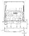
図1は、実施形態に係る電子部品ホルダ2を備える電気機器1の左側から見た斜視図である。図2は、同上の電気機器の右側から見た斜視図である。図1と図2に示すように、電子部品ホルダ2は、固定部21と、ホルダ本体3と、を備える。固定部21は、基板5に固定される。ホルダ本体3は、複数の収容凹部4(図4を参照)を有する。複数の収容凹部4は、基板5の一表面(第1の面51)側に開口している。基板5には、複数の電子部品E1が固定される。基板5の一表面には、複数の電子部品E1が配置される。複数の収容凹部4の各々は、複数の電子部品E1のうち少なくとも1つの対応する電子部品E1を保持する。
(1) Overview of Electronic Component Holder FIG. 1 is a left perspective view of an electric device 1 including an
本実施形態によれば、複数の電子部品E1の耐振動性を向上させることができる。 According to this embodiment, it is possible to improve the vibration resistance of the plurality of electronic components E1.
(2)電子部品及び基板
図3は、実施形態に係る電子部品ホルダ2を備える電気機器1の分解斜視図である。図3に示すように、複数の電子部品E1は、コンデンサ6と、抵抗器7と、を含む。コンデンサ6の個数は4個であり、抵抗器7の個数は2個である。すなわち、コンデンサ6の個数は、抵抗器7の個数よりも多い。また、基板5の厚さ方向から見て、複数のコンデンサ6が占める面積は、複数の抵抗器7が占める面積よりも大きい。
(2) Electronic Component and Substrate FIG. 3 is an exploded perspective view of the electrical device 1 including the
以下の説明では、図1~図7で矢印により示す方向によって、上下、左右及び前後の向きを規定する。ただし、これらの規定は、電子部品ホルダ2及び電気機器1の使用時の方向を限定する趣旨ではない。ここで規定する上下方向は、基板5の長手方向である。左右方向は、基板5の短手方向である。前後方向は、基板5の厚さ方向である。基板5から見てコンデンサ6側を前と規定し、コンデンサ6から見て基板5側を後と規定する。
In the following description, directions indicated by arrows in FIGS. 1 to 7 define up/down, left/right, and front/rear directions. However, these regulations are not intended to limit the directions in which the
図4は、実施形態に係る電子部品ホルダ2を備える電気機器1の背面図である。図4では、基板5を透過して2点鎖線で図示している。
FIG. 4 is a rear view of the electrical device 1 including the
各コンデンサ6は、より詳細には、電解コンデンサである。コンデンサ6は、リード部品である。図3と図4に示すように、コンデンサ6は、電子部品本体60と、電子部品本体60内部に収容されたコンデンサ素子(図示せず)と、2つのリード61と、を備えている。
Each
電子部品本体60の形状は、有底円筒状である。電子部品本体60の外形形状は、円柱状である。電子部品本体60は、天面601(前面)と、側面602と、引出面603(後面)と、を有している。天面601及び引出面603の形状は、円状である。引出面603は、基板5との対向面である。側面602は、天面601の外縁と引出面603とをつないでいる。電子部品本体60は、その内部に、コンデンサ素子を収容する収容空間を有している。電子部品本体60は、引出面603に、開口部604を有している。
The electronic component
2つのリード61は、コンデンサ素子に電気的に接続されている。2つのリード61は、電子部品本体60の引出面603から突出している。より詳細には、2つのリード61は、電子部品本体60の内部から開口部604を通して電子部品本体60の外部へ突出している。2つのリード61は、半田付けにより、基板5に固定される。
Two leads 61 are electrically connected to the capacitor element. The two leads 61 protrude from the
防爆弁(圧力弁とも言う)は、電解コンデンサ等の電子部品に備えられる。防爆弁は、電子部品のパッケージ内の圧力が耐圧を超えた際に開き、パッケージ内のガスを逃がす。コンデンサ6は、防爆弁62を有している。防爆弁62は、電子部品本体60(パッケージ)の天面601に設けられている。
An explosion-proof valve (also referred to as a pressure valve) is provided in an electronic component such as an electrolytic capacitor. The explosion-proof valve opens when the pressure inside the package of the electronic component exceeds the withstand voltage, allowing the gas inside the package to escape. The
コンデンサ6は、表示部63(図1を参照)を有している。表示部63には、所定の表示がされている。表示部63による表示の一例は、コンデンサ6の極性、容量及び耐電圧等である。表示部63は、例えば、電子部品本体60の側面602に文字、数字、記号又は模様等を付すことで設けられる。
The
コンデンサ6は、図4に示すように、開口部604を塞ぐ封止部材64を更に備えている。封止部材64を構成する材料は、例えば、EPT(ethylene-propyleneterpolymer)若しくはIIR(isobutylene‐isoprene rubber)等のゴム材料、又はエポキシ樹脂等の樹脂材料である。
The
抵抗器7は、より詳細には、セメント抵抗器である。また、抵抗器7は、リード部品である。抵抗器7は、電子部品本体70と、電子部品本体70内部に収容された抵抗素子と、2つのリード71と、を備えている。
抵抗素子は、金属等で形成されている。電子部品本体70は、セラミック製のケースであって、抵抗素子を収容している。電子部品本体70の外形形状は、直方体状である。電子部品本体70は、引出面703(後面)を有している。引出面703は、基板5との対向面である。2つのリード71は、抵抗素子に電気的に接続されている。2つのリード71は、引出面703から突出している。
The resistance element is made of metal or the like. The electronic component
図1に示すように、基板5は、第1の面51と、第2の面52と、を有している。第1の面51は、基板5の厚さ方向の一方側の面である。第2の面52は、第1の面51とは反対側の面である。複数の電子部品E1(4つのコンデンサ6及び2つの抵抗器7)は、第1の面51に配置される。すなわち、各コンデンサ6の電子部品本体60及び各抵抗器7の電子部品本体70は、第1の面51に配置される。各コンデンサ6の2つのリード61及び各抵抗器7の2つのリード71はそれぞれ、基板5に形成されたリード孔に挿入され、第2の面52に塗布される半田により基板5に半田付けされる。
As shown in FIG. 1,
また、図2と図4に示すように、基板5には、コネクタ55が実装される。コネクタ55は、端子台550と、複数(図4では6つ)のリード551と、を備えている。コネクタ55は、第1の面51上において、電子部品ホルダ2の外部に配置される。端子台550には、電線が接続される。複数のリード551は、端子台550から突出している。複数のリード551はそれぞれ、基板5に形成されたリード孔に挿入され、第2の面52に塗布される半田により基板5に半田付けされる。
A
(3)電子部品ホルダの詳細
ホルダ本体3は、例えば、樹脂を材料として形成されている。ホルダ本体3は、例えば、ポリエチレンテレフタレートを材料として形成されている。ホルダ本体3は、電気絶縁性を有している。よって、ホルダ本体3を設けることにより、ホルダ本体3が無い場合と比較して、複数の電子部品E1の各々と、ホルダ本体3の周囲に配置される部材との間の絶縁を強化することができる。
(3) Details of Electronic Component Holder The holder
図1と図4に示すように、ホルダ本体3は、後面(基板5との対向面)側が開口した箱状に形成されている。ホルダ本体3は、複数(図1と図4では4つ)の第1収容体31と、複数(図4では2つ)の第2収容体32と、を備えている。各第1収容体31の外形形状は、円柱状である。複数の第1収容体31は、複数のコンデンサ6と一対一で対応している。各第1収容体31は、対応するコンデンサ6を保持している。各第2収容体32の外形形状は、直方体状である。複数の第2収容体32は、複数の抵抗器7と一対一で対応している。各第2収容体32は、対応する抵抗器7を保持している。
As shown in FIGS. 1 and 4, the
図5は、実施形態に係る電子部品ホルダ2の背面図である。図6は、実施形態に係る電子部品ホルダ2の背面側から見た斜視図である。図4~図6に示すように、ホルダ本体3は、複数の収容凹部4として、複数(図4では4つ)の第1収容凹部4Aと、複数(図4では2つ)の第2収容凹部4Bと、を有している。各第1収容凹部4Aは、コンデンサ6(第1電子部品)を保持する。各第2収容凹部4Bは、第1電子部品とは形状が異なる抵抗器7(第2電子部品)を保持する。第2電子部品は、第1電子部品とは重さが異なる。複数の第1収容凹部4Aの内部空間と複数の第2収容凹部4Bの内部空間とがつながって、ホルダ本体3の内部空間を形成している。
FIG. 5 is a rear view of the
複数の収容凹部4と複数の電子部品E1とが一対一で対応している。複数の収容凹部4の各々には、複数の電子部品E1のうち対応する1つの電子部品E1が保持される。
The plurality of
複数の第1収容凹部4Aは、複数のコンデンサ6と一対一で対応している。各コンデンサ6は、対応する第1収容凹部4Aに保持されている。複数の第1収容凹部4Aは、複数の第1収容体31と一対一で対応している。各第1収容凹部4Aの内面は、対応する第1収容体31の内面を含んでいる。各第1収容凹部4Aは、対応する電子部品E1(コンデンサ6)を少なくとも左右から保持する。つまり、各第1収容凹部4Aは、対応する電子部品E1(コンデンサ6)を少なくとも左右から挟むように設けられている。
The plurality of
第1収容凹部4Aの形状は、コンデンサ6の外形に沿った形状である。第1収容凹部4Aは、内面として、底面41と、内側面42と、を含んでいる。底面41の形状は、円状である。内側面42は、底面41から後方へ延びている。内側面42の概略形状は、円筒の内周面に相当する形状である。コンデンサ6は、内側面42に囲まれる。第1収容凹部4Aとこれに隣り合う第1収容凹部4A又は第2収容凹部4Bとが連結している箇所には、後述する第1隔壁34の側面を除いて、内側面42が設けられていない。
The shape of the
複数の第2収容凹部4Bは、複数の抵抗器7と一対一で対応している。各抵抗器7は、対応する第2収容凹部4Bに保持されている。さらに、複数の第2収容凹部4Bは、複数の第2収容体32と一対一で対応している。各第2収容凹部4Bの内面は、対応する第2収容体32の内面を含んでいる。各第2収容凹部4Bは、対応する電子部品E1(抵抗器7)を少なくとも上下から保持する。つまり、各第2収容凹部4Bは、対応する電子部品E1(抵抗器7)を少なくとも上下から挟むように設けられている。
The plurality of
第2収容凹部4Bの形状は、抵抗器7の外形に沿った形状である。第2収容凹部4Bは、内面として、底面43と、内側面44と、を含んでいる。内側面44は、底面43から後方へ延びている。前後方向から見て、内側面44の形状は、角が実質的な直角のU字状である。抵抗器7は、少なくとも3方向から、内側面44に囲まれる。第2収容凹部4Bと第1収容凹部4Aとが連結している箇所には、内側面44が設けられていない。
The shape of the
前後方向における第1収容凹部4Aの長さ(深さ)は、前後方向における第2収容凹部4Bの長さ(深さ)よりも長い。つまり、ホルダ本体3の後端から、各第1収容凹部4Aは、第2収容凹部4Bと比較して深く窪んでいる。
The length (depth) of the
ホルダ本体3は、突出部33と、複数(図5では3つ)の第1隔壁34と、複数の第2隔壁35と、複数の第1リブ36と、複数の第2リブ37と、を備えている。
The
突出部33は、複数の第1収容凹部4Aの底面41から後方へ突出している。突出部33の突出量は、前後方向におけるホルダ本体3の高さよりも低い。突出部33の形状は、直方体状である。前後方向から見て、突出部33は、左右方向よりも上下方向に長い。突出部33は、複数(4つ)の第1収容凹部4Aの全てに亘って設けられている。より詳細には、突出部33は、ホルダ本体3の上端から下端までに亘って設けられている。
The
突出部33は、複数のコンデンサ6の天面601(図3参照)に対向する。これにより、天面601と底面41との間に隙間が確保される。突出部33は、複数のコンデンサ6の天面601に設けられた防爆弁62との間に隙間をあけて、天面601に対向している。突出部33は、天面601の全域との間に隙間をあけて、天面601に対向している。ここで、突出部33は、防爆弁62との間に隙間をあけていればよく、突出部33は、天面601の一部(例えば、防爆弁62の周囲の領域、又は、防爆弁62よりも前方に突出した部位)に接していてもよい。
The projecting
前後方向から見て、複数の第1隔壁34の各々の形状は、長方形状である。第1隔壁34は、複数の第1収容凹部4Aの底面41から後方へ突出している。各第1隔壁34の突出量は、突出部33の突出量よりも大きい。各第1隔壁34は、互いに隣り合う第1収容凹部4Aを隔てるように設けられている。つまり、各第1隔壁34の両側には、2つの第1収容凹部4Aの内部空間が存在する。各第1隔壁34の側面は、上記2つの第1収容凹部4Aの内側面42の一部を構成する。これにより、内側面42の少なくとも一部の範囲(底面41付近)は、周方向に連続している(図5と図6を参照)。
When viewed from the front-rear direction, each of the plurality of
第1隔壁34の両端には、第2隔壁35がつながっている。各第2隔壁35は、第1隔壁34から後方に延びている。各第2隔壁35の側面は、第1収容凹部4Aの内側面42の一部を構成する。
A
各第1収容凹部4Aの内側面42からは、複数(図5では3つ)の第1リブ36が突出している。複数の第1リブ36は、コンデンサ6(電子部品本体60)の側面602(図3を参照)に対向する。これにより、側面602と内側面42との間に隙間が確保される。複数の第1リブ36は、コンデンサ6の側面602に接してもよいし、接しなくてもよい。
A plurality of (three in FIG. 5)
各第2収容凹部4Bの内側面44からは、1又は複数の第2リブ37が突出している。図5では、2つの第2収容凹部4Bのうち一方(左側)の第2収容凹部4Bの内側面44からは、1つの第2リブ37が突出しており、2つの第2収容凹部4Bのうち他方(右側)の第2収容凹部4Bの内側面44からは、3つの第2リブ37が突出している。各第2リブ37は、抵抗器7(電子部品本体70)の側面に対向する。これにより、抵抗器7と内側面44との間に隙間が確保される。複数の第2リブ37は、抵抗器7の側面に接してもよいし、接しなくてもよい。
One or more
複数の収容凹部4のうち、複数の第1収容凹部4Aの各々は、リード部品としてのコンデンサ6を保持する。複数の第1収容凹部4Aの各々は、コンデンサ6の電子部品本体60の引出面603が基板5の第1の面51と対向する向きに、コンデンサ6を保持する。つまり、有底円筒状のコンデンサ6の軸方向が前後方向に沿うように、コンデンサ6が保持される。
Each of the plurality of
複数の収容凹部4のうち、複数の第2収容凹部4Bの各々は、リード部品としての抵抗器7を保持する。複数の第2収容凹部4Bの各々は、抵抗器7の電子部品本体70の引出面703が基板5の第1の面51と対向する向きに、抵抗器7を保持する。
Among the plurality of
図1に示すように、ホルダ本体3は、側面302を有している。側面302は、前後方向に沿った面である。側面302は、基板5の厚さ方向(前後方向)における複数の電子部品E1の両端間に亘って長さを有する。言い換えると、ホルダ本体3の後端(基板5との接触面)から底面41までの長さは、複数の電子部品E1(コンデンサ6及び抵抗器7)の高さ(前後方向の長さ)よりも長い。側面302は、複数の電子部品E1を覆う。
As shown in FIG. 1, the
側面302が複数の電子部品E1を覆っていることにより、複数の電子部品E1を保護できる。ホルダ本体3は、電気絶縁性を有しているので、側面302が複数の電子部品E1を覆っていることにより、側面302が複数の電子部品E1を覆っていない場合と比較して、複数の電子部品E1と周囲の構成との間の絶縁を強化できる。
By covering the plurality of electronic components E1 with the
ホルダ本体3は、その側面302に、複数(6つ。図1と図2を参照)の窓部38を有している。窓部38は、ホルダ本体3を貫通している貫通部である。そのため、ホルダ本体3は、窓部38において光を透過する。窓部38は、コンデンサ6の表示部63と対向する位置に設けられている。なお、窓部38は、ホルダ本体3を貫通している貫通部に限定されず、透光性を有する部材(アクリル樹脂等)から形成されていてもよい。
The
表示部63は、窓部38を通して視認される。図1では、コンデンサ6の極性を示す表示部63が、窓部38を通して視認される。つまり、図1で視認される帯状の表示部63が設けられた側が、コンデンサ6のマイナス端子側である。反対側(図2を参照)はプラス端子側であって、帯状の表示部63が設けられていない。このように、表示部63及び窓部38を設けることによって、複数のコンデンサ6が電子部品ホルダ2に保持された状態であっても、各コンデンサ6の極性を確認することができる。
The
窓部38はホルダ本体3を貫通している貫通部なので、窓部38を通して各コンデンサ6に放熱させることができる。
Since the
電子部品ホルダ2は、複数(図6では6つ)の固定部21を備えている。各固定部21は、例えば、金属製のピンである。各固定部21の形状は、T字状である(図1を参照)。各固定部21は、ホルダ本体3の後面(基板5との対向面)に設けられている。各固定部21の一部は、ホルダ本体3に埋め込まれており、ホルダ本体3から後方へ突出している。各固定部21は、例えば、インサート成形によりホルダ本体3と一体に形成されている。
The
基板5は、複数の取付穴を有している。複数の取付穴は、複数の固定部21と一対一で対応している。複数の固定部21のそれぞれの先端部は、対応する取付孔に挿入され、第2の面52に塗布される半田により基板5に半田付けされる。
The
複数の電子部品E1と電子部品ホルダ2とのいずれも、半田付けにより基板5に固定される。そのため、複数の電子部品E1と電子部品ホルダ2とを、同一の工程で基板5に固定することができる。これにより、複数の電子部品E1を基板5に固定する工程と電子部品ホルダ2を基板5に固定する工程とが異なる場合と比較して、工数を削減することができる。なお、複数の電子部品E1と電子部品ホルダ2とを半田付けにより基板5に固定する工程で、コネクタ55も半田付けにより基板5に固定することができる。
Both the electronic components E1 and the
ここで、防爆弁を有する電子部品E1を特定電子部品と呼ぶことにすると、防爆弁62を有するコンデンサ6は、特定電子部品である。また、特定電子部品が保持される収容凹部4を特定収容凹部と呼ぶことにすると、コンデンサ6が保持される第1収容凹部4Aは、特定収容凹部である。第1収容凹部4Aの底面41は、閉塞しており、コンデンサ6の防爆弁62と対向する。ここで、「閉塞している」とは、孔等が存在しないことを指す。底面41が閉塞しているため、底面41から空気等が漏れることを抑制できる。底面41に孔が設けられている場合と比較して、防爆弁62が開いた際に、防爆弁62の周囲に供給される酸素量を低減できる。よって、防爆弁62から出るガスが引火する可能性を低減し、引火した場合であっても、燃え続ける可能性を低減できる。
Here, if the electronic component E1 having the explosion-proof valve is called a specific electronic component, the
第1収容凹部4A(特定収容凹部)は、底面41と防爆弁62との間に隙間をあけて、コンデンサ6(特定電子部品)を保持する。つまり、防爆弁62がスムーズに開くように、隙間が設けられている。より詳細には、ホルダ本体3は、第1収容凹部4A(特定収容凹部)の底面41から突出した突出部33を有し、突出部33により、底面41と防爆弁62との間に隙間が確保されている。また、ホルダ本体3の後端(基板5との接触面)から底面41までの長さが、コンデンサ6の高さ(前後方向の長さ)よりも長いことによって、底面41と防爆弁62との間に隙間が確保されている。
The
コンデンサ6の天面601(防爆弁62)と底面41との間の隙間は、側面602と内側面42との間の隙間よりも大きい。これにより、防爆弁62と底面41とが干渉する可能性を低減できる。
The gap between the top surface 601 (explosion-proof valve 62 ) of the
基板5の厚さ方向から見て(より詳細には、前から見て)、ホルダ本体3は、複数の電子部品E1の各々の全体を覆う。これにより、複数の電子部品E1を保護できる。ホルダ本体3は、電気絶縁性を有し、かつ、前から見て複数の電子部品E1の各々の全体を覆っているので、前から見て複数の電子部品E1がホルダ本体3に覆われていない場合と比較して、複数の電子部品E1とホルダ本体3の前方に設けられた構成との間の絶縁を強化できる。
When viewed from the thickness direction of the substrate 5 (more specifically, viewed from the front), the
(4)配置
図4に示すように、複数(4つ)の第1収容凹部4Aは、全体として上下方向に沿って並んでいる。これにより、複数(4つ)のコンデンサ6が、全体として上下方向に沿って並ぶ。ここで、4つの第1収容凹部4Aのうち1つの第1収容凹部4A(上から3つ目の第1収容凹部4A)は、残りの3つの第1収容凹部4Aに対して右にずれて配置されている。これに応じて、4つのコンデンサ6のうち1つのコンデンサ6(上から3つ目のコンデンサ6)は、残りの3つのコンデンサ6に対して右にずれて配置される。
(4) Arrangement As shown in FIG. 4, the plurality (four) of
複数の第1収容凹部4Aに3つ以上のコンデンサ6が保持されているとき、基板5の厚さ方向から見て、3つ以上のコンデンサ6の各々の基準点G1を、コンデンサ6の重心、又は、コンデンサ6が備える複数のリード61の重心と定義する。本実施形態では、第1収容凹部4Aの個数及びコンデンサ6の個数はそれぞれ4つである。つまり、4つの第1収容凹部4Aに4つのコンデンサ6が保持されているとき、基板5の厚さ方向から見て、4つのコンデンサ6の各々の基準点G1を、コンデンサ6の重心、又は、コンデンサ6が備える複数のリード61の重心と定義する。なお、重心は、空間的な重心であってもよいし、質量を考慮した重心(質量中心)であってもよい。本実施形態では、空間的な重心と質量中心とが一致する。さらに、コンデンサ6の重心と複数のリード61の重心とは、一致する。
When three or
基板5の厚さ方向から見て、4つのコンデンサ6のうち2つのコンデンサ6(上から1つ目及び2つ目のコンデンサ6)のそれぞれの基準点G1を結ぶ直線SL1上に、別の1つのコンデンサ6(上から4つ目のコンデンサ6)の基準点G1がある。基板5の厚さ方向から見て、直線SL1上とは異なる位置に、残りの1つのコンデンサ6(上から3つ目のコンデンサ6)の基準点G1がある。
When viewed from the thickness direction of the
4つのコンデンサ6がこのように配置されることで、4つのコンデンサ6の基準点G1が直線SL1上に位置する場合と比較して、各コンデンサ6が同時に、同方向に振動して共振が起きる可能性を低減できる。すなわち、基板5又は電子部品ホルダ2に振動が加わった場合に、4つのコンデンサ6の基準点G1が直線SL1上にある場合と比較して、各コンデンサ6がそれぞれ異なるタイミング及び異なる方向に振動する可能性が高くなる。よって、各コンデンサ6の耐振動性を向上させることができる。
By arranging the four
また、2つの抵抗器7の各々の基準点G1を、抵抗器7の重心、又は、抵抗器7が備える複数のリード71の重心と定義する。抵抗器7の重心と複数のリード71の重心とは、一致する。基板5の厚さ方向から見て、直線SL1上とは異なる位置に、2つの抵抗器7のそれぞれの基準点G1がある。
Also, the reference point G1 of each of the two
また、コンデンサ6の2つのリード61は、2つのリード61が並ぶ方向(左右方向)と直交する方向(上下方向)に折れて破断されやすい。ここで、4つの第1収容凹部4Aは、コンデンサ6の2つのリード61が並ぶ方向(左右方向)と直交する方向(上下方向)に沿って並んでいる。そのため、基板5又は電子部品ホルダ2に上下方向の振動が加わった場合に、複数のコンデンサ6が互いを支持し、複数のコンデンサ6の振動を低減できる。よって、2つのリード61が破断する可能性を低減できる。本実施形態では、同一直線上(例えば、直線SL1上)に、4つの第1収容凹部4Aの各々の一部が存在している。
Also, the two leads 61 of the
(5)電気機器
図7は、実施形態に係る電子部品ホルダ2を備える電気機器1の右側面図である。図7に示すように、電気機器1は、電子部品ホルダ2と、基板5と、複数の電子部品E1と、を備えている。電気機器1は、サーボアンプである。サーボアンプは、サーボモータの動作を制御する。より詳細には、サーボアンプは、上位コントローラからの動作指令並びにサーボモータの回転角、速度及びトルク等のフィードバック値に基づいてサーボモータに電力を供給することで、サーボモータの動作を制御する。電気機器1は、サーボアンプとしての機能を実現するための制御回路10を備えている。制御回路10は、複数の電子部品E1と、複数の回路基板11、12と、を含む。
(5) Electric Equipment FIG. 7 is a right side view of the electric equipment 1 including the
電気機器1は、筐体8を更に備えている。筐体8は、電子部品ホルダ2と、基板5と、複数の電子部品E1と、を収容している。筐体8は、本体81と、カバー82と、を有している。本体81は、後面が開口した箱状に形成されている。カバー82は、本体81の後面を覆う。
The electrical equipment 1 further includes a
一例として、基板5は、その長手方向が鉛直方向(上下方向)に沿うように配置される。
As an example, the
筐体8は、例えば、アルミニウムを材料として形成されている。電子部品ホルダ2を設けたことにより、電子部品ホルダ2が無い場合と比較して、複数の電子部品E1と筐体8及び複数の回路基板11、12との間の絶縁を強化することができる。
The
(6)利点
電気機器1が移動する場合等に、電気機器1の複数の電子部品E1のそれぞれが振動することがある。複数の電子部品E1のそれぞれが振動することで、複数の電子部品E1の一部(例えば、リード61又は71)が折れて破断する等の弊害が起きる可能性がある。ここで、それぞれの電子部品E1が振動する場合に、振動数によって、電子部品E1の一部の破断する可能性の高低が異なる。ある電子部品E1について、電子部品E1の一部の破断される可能性が比較的高い振動数を、その電子部品E1の固有振動数と呼ぶ。固有振動数は、電子部品E1の形状、基板5上での位置、基板5における電子部品E1の支持点の位置、及び、基板5への固定手段等によって決まる。
(6) Advantages When the electric device 1 moves, each of the electronic components E1 of the electric device 1 may vibrate. When each of the electronic components E1 vibrates, there is a possibility that some of the electronic components E1 (for example, the
複数の電子部品E1は、単一の電子部品ホルダ2に保持される。そのため、複数の電子部品E1が互いを支持し、複数の電子部品E1の振動を低減できる。複数の電子部品E1が互いを支持することで、固有振動数の振動を打ち消すことができる。このように、複数の電子部品E1の耐振動性を向上させることができる。例えば、電気機器1(サーボアンプ)とサーボモータとを含むシステムの全体に振動が加わり得る環境下での複数の電子部品E1の耐振動性を向上させることができる。また、サーボモータの振動が電気機器1に伝搬する場合の複数の電子部品E1の耐振動性を向上させることができる。
A plurality of electronic components E1 are held by a single
また、本実施形態によれば、複数の電子部品E1に電子部品ホルダ2を被せるという簡素な手段で、複数の電子部品E1を保持できる。
Further, according to the present embodiment, a plurality of electronic components E1 can be held by a simple means of covering the plurality of electronic components E1 with the
(実施形態の変形例)
以下、実施形態の変形例を列挙する。以下の変形例は、適宜組み合わせて実現されてもよい。
(Modification of embodiment)
Modifications of the embodiment are listed below. The following modified examples may be implemented in combination as appropriate.
複数の収容凹部4のうち少なくとも一部の収容凹部4は、2つ以上の電子部品E1を保持してもよい。
At least some of the plurality of
実施形態における収容凹部4、電子部品E1及び固定部21等の個数は一例であり、適宜変更が可能である。
The numbers of the
電子部品E1は、コンデンサ6及び抵抗器7に限定されない。電子部品E1は、例えば、半導体素子、スイッチ素子、又はコイル等であってもよい。
Electronic component E1 is not limited to
ホルダ本体3は、基板5と共に、複数の電子部品E1の全体を覆っていてもよい。すなわち、基板5が複数の電子部品E1を後ろから覆い、ホルダ本体3が複数の電子部品E1を前、左右及び上下から覆ってもよい。
The holder
電子部品ホルダ2を基板5に固定する手段は、半田付けに限定されず、例えば、接着、嵌め込み、又は、圧着であってもよい。ただし、手段として半田付けを用いると、電子部品E1と固定部21とを半田付けを伴う同一の工程により基板5に固定することができるので好ましい。固定部21の構成は、電子部品ホルダ2を基板5に固定する手段に応じて、適宜変更が可能である。
The means for fixing the
複数の電子部品E1の向きは、実施形態で述べた向きに限定されない。例えば、各コンデンサ6が備える2つのリード61が並んでいる向きを、互いに隣り合うコンデンサ6間で異ならせてもよい。例えば、あるコンデンサ6では、2つのリード61を上下に並べ、このコンデンサ6と隣り合う1つ又は2つコンデンサ6では、2つのリード61を左右に並べてもよい。
The directions of the plurality of electronic components E1 are not limited to the directions described in the embodiments. For example, the directions in which the two leads 61 of each
電子部品本体60の外形形状は、円柱状に限定されない。電子部品本体60は、基板5の厚さ方向から見て、第1方向の長さが、第1方向と直交する第2方向の長さよりも短い形状であってもよい。電子部品本体60は、例えば、直方体状であってもよい。ここで、第1方向は、複数の第1収容凹部4Aが並んでいる方向(実施形態では上下方向)に沿っていることが好ましい。これにより、電子部品ホルダ2の最長の長さを短くし、複数の電子部品E1に生じる振動の大きさを低減できる。
The external shape of electronic component
(まとめ)
以上説明した実施形態等から、以下の態様が開示されている。
(summary)
The following aspects are disclosed from the embodiments and the like described above.
第1の態様に係る電子部品ホルダ(2)は、固定部(21)と、ホルダ本体(3)と、を備える。固定部(21)は、基板(5)に固定される。ホルダ本体(3)は、複数の収容凹部(4)を有する。複数の収容凹部(4)は、基板(5)の一表面(第1の面51)側に開口している。基板(5)には、複数の電子部品(E1)が固定される。基板(5)の一表面には、複数の電子部品(E1)が配置される。複数の収容凹部(4)の各々は、複数の電子部品(E1)のうち少なくとも1つの対応する電子部品(E1)を保持する。 An electronic component holder (2) according to a first aspect includes a fixing portion (21) and a holder body (3). The fixed part (21) is fixed to the substrate (5). The holder body (3) has a plurality of accommodation recesses (4). The plurality of accommodation recesses (4) are open to one surface (first surface 51) of the substrate (5). A plurality of electronic components (E1) are fixed to the substrate (5). A plurality of electronic components (E1) are arranged on one surface of the substrate (5). Each of the plurality of housing recesses (4) holds at least one corresponding electronic component (E1) among the plurality of electronic components (E1).
上記の構成によれば、複数の電子部品(E1)の耐振動性を向上させることができる。 According to the above configuration, it is possible to improve the vibration resistance of the plurality of electronic components (E1).
また、第2の態様に係る電子部品ホルダ(2)では、第1の態様において、基板(5)の一表面(第1の面51)には、複数の電子部品(E1)として、3つ以上の電子部品(E1)が配置される。複数の収容凹部(4)に3つ以上の電子部品(E1)が保持されているとき、基板(5)の厚さ方向から見て、3つ以上の電子部品(E1)の各々の基準点(G1)を、電子部品(E1)の重心、又は、電子部品(E1)が備える1又は複数のリード(61、71)の重心と定義する。3つ以上の電子部品(E1)のうち2つの電子部品(E1)のそれぞれの基準点(G1)を結ぶ直線(SL1)上とは異なる位置に、3つ以上の電子部品(E1)のうち少なくとも1つの電子部品(E1)の基準点(G1)がある。 Further, in the electronic component holder (2) according to the second aspect, in the first aspect, three electronic components (E1) are provided on one surface (first surface 51) of the substrate (5). The above electronic components (E1) are arranged. When three or more electronic components (E1) are held in a plurality of housing recesses (4), reference points for each of the three or more electronic components (E1) when viewed from the thickness direction of the substrate (5) (G1) is defined as the center of gravity of the electronic component (E1) or the center of gravity of one or more leads (61, 71) of the electronic component (E1). At a position different from the straight line (SL1) connecting the respective reference points (G1) of two electronic components (E1) among the three or more electronic components (E1), among the three or more electronic components (E1) There is a reference point (G1) of at least one electronic component (E1).
上記の構成によれば、全ての電子部品(E1)の基準点(G1)が直線(SL1)上に位置する場合と比較して、各電子部品(E1)が同時に、同方向に振動して共振が起きる可能性を低減できる。よって、各電子部品(E1)の耐振動性を更に向上させることができる。 According to the above configuration, each electronic component (E1) simultaneously vibrates in the same direction as compared with the case where the reference points (G1) of all the electronic components (E1) are positioned on the straight line (SL1). The possibility of resonance occurring can be reduced. Therefore, the vibration resistance of each electronic component (E1) can be further improved.
また、第3の態様に係る電子部品ホルダ(2)では、第1又は2の態様において、複数の電子部品(E1)は、防爆弁(62)を有する特定電子部品(コンデンサ6)を含む。複数の収容凹部(4)のうち、特定電子部品が保持される特定収容凹部(第1収容凹部4A)の底面(41)は、閉塞しており、防爆弁(62)と対向する。
Further, in the electronic component holder (2) according to the third aspect, in the first or second aspect, the plurality of electronic components (E1) include the specific electronic component (capacitor 6) having the explosion-proof valve (62). Of the plurality of accommodation recesses (4), the bottom surface (41) of the specific accommodation recess (
上記の構成によれば、底面(41)に孔が設けられている場合と比較して、防爆弁(62)が開いた際に、防爆弁(62)の周囲に供給される酸素量を低減できる。よって、防爆弁(62)から出るガスが引火する可能性を低減し、引火した場合であっても、燃え続ける可能性を低減できる。 According to the above configuration, the amount of oxygen supplied around the explosion-proof valve (62) when the explosion-proof valve (62) is opened is reduced compared to the case where the bottom surface (41) is provided with holes. can. Therefore, it is possible to reduce the possibility that the gas emitted from the explosion-proof valve (62) will catch fire, and even if it catches fire, the possibility that it will continue to burn can be reduced.
また、第4の態様に係る電子部品ホルダ(2)では、第3の態様において、特定収容凹部(第1収容凹部4A)は、底面(41)と、防爆弁(62)との間に隙間をあけて、特定電子部品(コンデンサ6)を保持する。
Further, in the electronic component holder (2) according to the fourth aspect, in the third aspect, the specific accommodation recess (
上記の構成によれば、防爆弁(62)が開く際に、防爆弁(62)と特定収容凹部(第1収容凹部4A)の底面(41)とが干渉する可能性を低減できる。
According to the above configuration, when the explosion-proof valve (62) is opened, the possibility of interference between the explosion-proof valve (62) and the bottom surface (41) of the specific accommodation recess (
また、第5の態様に係る電子部品ホルダ(2)では、第4の態様において、ホルダ本体(3)は、突出部(33)を有する。突出部(33)は、特定収容凹部(第1収容凹部4A)の底面(41)から突出している。
Further, in the electronic component holder (2) according to the fifth aspect, in the fourth aspect, the holder main body (3) has a protrusion (33). The protrusion (33) protrudes from the bottom surface (41) of the specific accommodation recess (
上記の構成によれば、防爆弁(62)と特定収容凹部(第1収容凹部4A)の底面(41)との隙間を確保できる可能性が高まる。
According to the above configuration, it is more likely that a gap can be secured between the explosion-proof valve (62) and the bottom surface (41) of the specific accommodation recess (
また、第6の態様に係る電子部品ホルダ(2)では、第1~5の態様のいずれか1つにおいて、ホルダ本体(3)は、側面(302)を有する。側面(302)は、基板(5)の厚さ方向における複数の電子部品(E1)の両端間に亘って長さを有し、複数の電子部品(E1)を覆う。 Further, in the electronic component holder (2) according to the sixth aspect, in any one of the first to fifth aspects, the holder body (3) has a side surface (302). The side surface (302) has a length extending between both ends of the plurality of electronic components (E1) in the thickness direction of the substrate (5) and covers the plurality of electronic components (E1).
上記の構成によれば、複数の電子部品(E1)を保護できる。 According to the above configuration, it is possible to protect a plurality of electronic components (E1).
また、第7の態様に係る電子部品ホルダ(2)では、第6の態様において、複数の電子部品(E1)のうち少なくとも1つの電子部品(E1)は、表示部(63)を有する。表示部(63)には、所定の表示がされている。側面(302)は、表示部(63)と対向する位置に、窓部(38)を有している。窓部(38)は、光を透過する。 Further, in the electronic component holder (2) according to the seventh aspect, in the sixth aspect, at least one electronic component (E1) among the plurality of electronic components (E1) has a display section (63). A predetermined display is made on the display section (63). The side surface (302) has a window (38) at a position facing the display (63). The window (38) is transparent to light.
上記の構成によれば、複数の電子部品(E1)の各々が収容凹部(4)に保持された状態であっても、表示部(63)を視認することが可能となる。 According to the above configuration, the display section (63) can be viewed even when each of the plurality of electronic components (E1) is held in the housing recess (4).
また、第8の態様に係る電子部品ホルダ(2)では、第1~7の態様のいずれか1つにおいて、複数の電子部品(E1)は、第1電子部品(コンデンサ6)と、第2電子部品(抵抗器7)と、を含む。第2電子部品は、第1電子部品とは形状が異なる。複数の収容凹部(4)は、第1電子部品を保持する第1収容凹部(4A)と、第2電子部品を保持する第2収容凹部(4B)と、を含む。 Further, in the electronic component holder (2) according to the eighth aspect, in any one of the first to seventh aspects, the plurality of electronic components (E1) include a first electronic component (capacitor 6) and a second electronic component (capacitor 6). and an electronic component (resistor 7). The second electronic component is different in shape from the first electronic component. The plurality of accommodation recesses (4) includes a first accommodation recess (4A) that holds the first electronic component and a second accommodation recess (4B) that holds the second electronic component.
上記の構成によれば、1つの電子部品ホルダ(2)により、第1電子部品(コンデンサ6)と第2電子部品(抵抗器7)との両方を保持できる。 According to the above configuration, one electronic component holder (2) can hold both the first electronic component (capacitor 6) and the second electronic component (resistor 7).
また、第9の態様に係る電子部品ホルダ(2)では、第1~8の態様のいずれか1つにおいて、固定部(21)は、半田付けにより基板(5)に固定される。 Further, in the electronic component holder (2) according to the ninth aspect, in any one of the first to eighth aspects, the fixing portion (21) is fixed to the substrate (5) by soldering.
上記の構成によれば、複数の電子部品(E1)のうち少なくとも一部の電子部品(E1)が半田付けにより基板(5)に固定される場合に、電子部品(E1)と固定部(21)とを半田付けを伴う同一の工程により基板(5)に固定することができる。 According to the above configuration, when at least some electronic components (E1) among the plurality of electronic components (E1) are fixed to the substrate (5) by soldering, the electronic components (E1) and the fixing portion (21) ) can be fixed to the substrate (5) by the same process involving soldering.
また、第10の態様に係る電子部品ホルダ(2)では、第1~9の態様のいずれか1つにおいて、複数の電子部品(E1)は、リード部品(コンデンサ6)を含む。リード部品は、2つのリード(61)を備える。複数の収容凹部(4)のうち、リード部品を保持する収容凹部(4)を含む2以上の収容凹部(4)は、2つのリード(61)が並ぶ方向と直交する方向に沿って並んでいる。 Further, in the electronic component holder (2) according to the tenth aspect, in any one of the first to ninth aspects, the plurality of electronic components (E1) include lead components (capacitors 6). The lead component comprises two leads (61). Among the plurality of housing recesses (4), two or more housing recesses (4) including a housing recess (4) for holding a lead component are arranged along a direction perpendicular to the direction in which two leads (61) are arranged. there is
上記の構成によれば、複数の電子部品(E1)が並んでいることにより、複数の電子部品(E1)が並んでいる方向の振動が抑制される。複数の電子部品(E1)が並んでいる方向は、各リード(61)が折れて破断されやすい方向と実質的に一致する。よって、各リード(61)が破断する可能性を低減できる。 According to the above configuration, by arranging the plurality of electronic components (E1), vibration in the direction in which the plurality of electronic components (E1) are arranged is suppressed. The direction in which the plurality of electronic components (E1) are arranged substantially coincides with the direction in which each lead (61) is likely to break and break. Therefore, it is possible to reduce the possibility of each lead (61) breaking.
また、第11の態様に係る電子部品ホルダ(2)では、第1~10の態様のいずれか1つにおいて、基板(5)の厚さ方向から見て、ホルダ本体(3)は、複数の電子部品(E1)の全体を覆う。 Further, in the electronic component holder (2) according to the eleventh aspect, in any one of the first to tenth aspects, when viewed from the thickness direction of the substrate (5), the holder body (3) has a plurality of It covers the entire electronic component (E1).
上記の構成によれば、複数の電子部品(E1)を保護できる。 According to the above configuration, it is possible to protect a plurality of electronic components (E1).
また、第12の態様に係る電子部品ホルダ(2)では、第1~11の態様のいずれか1つにおいて、ホルダ本体(3)は、樹脂を材料として形成されている。 Further, in the electronic component holder (2) according to the twelfth aspect, in any one of the first to eleventh aspects, the holder body (3) is made of resin.
上記の構成によれば、ホルダ本体(3)の成形が容易である。 According to the above configuration, it is easy to mold the holder body (3).
また、第13の態様に係る電子部品ホルダ(2)では、第1~12の態様のいずれか1つにおいて、複数の電子部品(E1)は、リード部品(コンデンサ6及び抵抗器7)を含む。リード部品は、引出面(603、703)を有する電子部品本体(60、70)と、引出面(603、703)から突出したリード(61、71)と、を備える。複数の収容凹部(4)のうち、リード部品を保持する収容凹部(4)は、引出面(603、703)が基板(5)の一表面(第1の面51)と対向する向きに、電子部品本体(60、70)を保持する。
Further, in the electronic component holder (2) according to the thirteenth aspect, in any one of the first to twelfth aspects, the plurality of electronic components (E1) includes lead components (
上記の構成によれば、1又は複数のリード(61、71)の折れ曲がりを無くす又は折れ曲がり箇所を少なくできる。よって、1又は複数のリード(61、71)が破断する可能性を低減できる。 According to the above configuration, bending of one or more leads (61, 71) can be eliminated or the number of bent portions can be reduced. Therefore, it is possible to reduce the possibility of one or more leads (61, 71) breaking.
また、第14の態様に係る電子部品ホルダ(2)では、第1~13の態様のいずれか1つにおいて、複数の収容凹部(4)の各々には、複数の電子部品(E1)のうち対応する1つの電子部品(E1)が保持される。 Further, in the electronic component holder (2) according to the fourteenth aspect, in any one of the first to thirteenth aspects, each of the plurality of accommodation recesses (4) includes, among the plurality of electronic components (E1) One corresponding electronic component (E1) is retained.
上記の構成によれば、複数の電子部品(E1)の耐振動性を更に向上させることができる。 According to the above configuration, it is possible to further improve the vibration resistance of the plurality of electronic components (E1).
第1の態様以外の構成については、電子部品ホルダ(2)に必須の構成ではなく、適宜省略可能である。 Configurations other than the first aspect are not essential to the electronic component holder (2), and can be omitted as appropriate.
また、第15の態様に係る電気機器(1)では、第1~14の態様のいずれか1つに係る電子部品ホルダ(2)と、基板(5)と、複数の電子部品(E1)と、を備える。 Further, in the electric device (1) according to the fifteenth aspect, the electronic component holder (2) according to any one of the first to fourteenth aspects, the substrate (5), and the plurality of electronic components (E1) , provided.
上記の構成によれば、複数の電子部品(E1)の耐振動性を向上させることができる。 According to the above configuration, it is possible to improve the vibration resistance of the plurality of electronic components (E1).
また、第16の態様に係る電気機器(1)は、第15の態様において、サーボモータの動作を制御するサーボアンプである。 Further, the electric device (1) according to the sixteenth aspect is the servo amplifier that controls the operation of the servomotor in the fifteenth aspect.
上記の構成によれば、複数の電子部品(E1)の耐振動性を向上させることができる。 According to the above configuration, it is possible to improve the vibration resistance of the plurality of electronic components (E1).
1 電気機器
2 電子部品ホルダ
3 ホルダ本体
4 収容凹部
4A 第1収容凹部(特定収容凹部)
4B 第2収容凹部
5 基板
6 コンデンサ(特定電子部品、第1電子部品、リード部品)
7 抵抗器(第2電子部品、リード部品)
8 筐体
10 制御回路
11 回路基板
12 回路基板
21 固定部
31 第1収容体
32 第2収容体
33 突出部
34 第1隔壁
35 第2隔壁
36 第1リブ
37 第2リブ
38 窓部
41 底面
42 内側面
43 底面
44 内側面
51 第1の面(一表面)
52 第2の面
55 コネクタ
60 電子部品本体(パッケージ)
61 リード
62 防爆弁
63 表示部
64 封止部材
70 電子部品本体
71 リード
81 本体
82 カバー
302 側面
550 端子台
551 リード
601 天面
602 側面
603 引出面
604 開口部
703 引出面
E1 電子部品
G1 基準点
SL1 直線
1
4B
7 resistor (second electronic component, lead component)
8
52
61
Claims (16)
前記複数の収容凹部に前記3つ以上の電子部品が保持されているとき、前記基板の厚さ方向から見て、前記3つ以上の電子部品の各々の基準点を、前記電子部品の重心、又は、前記電子部品が備える1又は複数のリードの重心と定義すると、
前記3つ以上の電子部品のうち2つの電子部品のそれぞれの前記基準点を結ぶ直線上とは異なる位置に、前記3つ以上の電子部品のうち少なくとも1つの電子部品の前記基準点がある、請求項1に記載の電子部品ホルダ。 three or more electronic components are arranged as the plurality of electronic components on the one surface of the substrate;
When the three or more electronic components are held in the plurality of housing recesses, the reference point of each of the three or more electronic components is the center of gravity of the electronic component when viewed from the thickness direction of the substrate. Alternatively, when defined as the center of gravity of one or more leads provided in the electronic component,
The reference point of at least one of the three or more electronic components is at a position different from the straight line connecting the reference points of two of the three or more electronic components, The electronic component holder according to claim 1.
前記基板の厚さ方向における前記複数の電子部品の両端間に亘って長さを有し、前記複数の電子部品を覆う側面を有する、請求項1~5のいずれか一項に記載の電子部品ホルダ。 The holder main body is
The electronic component according to any one of claims 1 to 5, having a length extending between both ends of the plurality of electronic components in the thickness direction of the substrate and having a side surface covering the plurality of electronic components. holder.
前記複数の収容凹部のうち、前記リード部品を保持する収容凹部を含む2以上の収容凹部は、前記2つのリードが並ぶ方向と直交する方向に沿って並んでいる、請求項1~9のいずれか一項に記載の電子部品ホルダ。 The plurality of electronic components includes a lead component having two leads,
10. The storage recess according to any one of claims 1 to 9, wherein, of said plurality of storage recesses, two or more storage recesses including a storage recess for holding said lead component are arranged along a direction orthogonal to a direction in which said two leads are arranged. or the electronic component holder according to claim 1.
請求項1~10のいずれか一項に記載の電子部品ホルダ。 When viewed from the thickness direction of the substrate, the holder body covers the entirety of the plurality of electronic components,
The electronic component holder according to any one of claims 1-10.
請求項1~12のいずれか一項に記載の電子部品ホルダ。 The plurality of electronic components includes a lead component having an electronic component body having a lead-out surface and a lead projecting from the lead-out surface, and among the plurality of accommodation recesses, the accommodation recess for holding the lead component is , holding the electronic component body in a direction in which the lead surface faces the one surface of the substrate;
The electronic component holder according to any one of claims 1-12.
Applications Claiming Priority (2)
| Application Number | Priority Date | Filing Date | Title |
|---|---|---|---|
| JP2020028825 | 2020-02-21 | ||
| PCT/JP2021/001561 WO2021166520A1 (en) | 2020-02-21 | 2021-01-19 | Electronic component holder and electrical instrument |
Publications (2)
| Publication Number | Publication Date |
|---|---|
| JPWO2021166520A1 JPWO2021166520A1 (en) | 2021-08-26 |
| JPWO2021166520A5 true JPWO2021166520A5 (en) | 2022-10-18 |
Family
ID=77392100
Family Applications (1)
| Application Number | Title | Priority Date | Filing Date |
|---|---|---|---|
| JP2022501705A Pending JPWO2021166520A1 (en) | 2020-02-21 | 2021-01-19 |
Country Status (4)
| Country | Link |
|---|---|
| EP (1) | EP4109480A4 (en) |
| JP (1) | JPWO2021166520A1 (en) |
| CN (1) | CN115088046A (en) |
| WO (1) | WO2021166520A1 (en) |
Families Citing this family (1)
| Publication number | Priority date | Publication date | Assignee | Title |
|---|---|---|---|---|
| WO2023166702A1 (en) * | 2022-03-04 | 2023-09-07 | 株式会社オートネットワーク技術研究所 | Power supply unit |
Family Cites Families (16)
| Publication number | Priority date | Publication date | Assignee | Title |
|---|---|---|---|---|
| JPS53149674A (en) * | 1977-05-31 | 1978-12-27 | Matsushita Electric Works Ltd | Device for holding electric part |
| JPS542368U (en) * | 1977-06-09 | 1979-01-09 | ||
| JPS5910738Y2 (en) * | 1978-09-18 | 1984-04-04 | ティーディーケイ株式会社 | Capacitor mounting structure |
| JPS55164873U (en) * | 1979-05-15 | 1980-11-27 | ||
| JP4226226B2 (en) * | 2001-02-22 | 2009-02-18 | パナソニック株式会社 | Circuit formation method |
| US6631071B2 (en) * | 2002-01-16 | 2003-10-07 | Matsushita Electric Industrial Co., Ltd. | Capacitor module |
| JP3641807B2 (en) * | 2002-09-05 | 2005-04-27 | 三菱電機株式会社 | Conversion unit of power converter |
| JP2006049649A (en) * | 2004-08-05 | 2006-02-16 | Denso Corp | Spacer for mounting |
| JP2007220794A (en) * | 2006-02-15 | 2007-08-30 | Toyota Motor Corp | Capacitor device |
| JP2007281127A (en) * | 2006-04-05 | 2007-10-25 | Shindengen Electric Mfg Co Ltd | Circuit device equipped with capacitor, and capacitor module |
| DE102009046403B4 (en) * | 2009-11-04 | 2015-05-28 | Semikron Elektronik Gmbh & Co. Kg | Power semiconductor module in pressure contact technology |
| JP2011129836A (en) * | 2009-12-21 | 2011-06-30 | Origin Electric Co Ltd | Electronic component holder, and method and structure for mounting electronic component |
| DE102012201753A1 (en) * | 2012-02-07 | 2013-08-08 | Zf Friedrichshafen Ag | Capacitor used in power electronic circuit of hybrid vehicle, has case that is arranged for fastening capacitor between coils, such that longitudinal extension axis of case and winding axis of coils are aligned parallel to each other |
| JP2017168778A (en) * | 2016-03-18 | 2017-09-21 | パナソニックIpマネジメント株式会社 | Cooling structure of electrolytic capacitor and electrolytic capacitor unit |
| JP2019195003A (en) * | 2016-09-07 | 2019-11-07 | パナソニックIpマネジメント株式会社 | Electronic component mounting body, electronic controller, and servo motor |
| JP6416993B1 (en) | 2017-07-06 | 2018-10-31 | イリソ電子工業株式会社 | Capacitor holder |
-
2021
- 2021-01-19 CN CN202180014900.XA patent/CN115088046A/en active Pending
- 2021-01-19 EP EP21757139.7A patent/EP4109480A4/en active Pending
- 2021-01-19 JP JP2022501705A patent/JPWO2021166520A1/ja active Pending
- 2021-01-19 WO PCT/JP2021/001561 patent/WO2021166520A1/en unknown
Similar Documents
| Publication | Publication Date | Title |
|---|---|---|
| US10615394B2 (en) | Energy storage apparatus | |
| JP6062530B2 (en) | Electronic component assembly structure and electrical junction box | |
| JP6115465B2 (en) | Electronic control unit and electric power steering apparatus using the same | |
| JP6582016B2 (en) | Electrical junction box | |
| WO2017002584A1 (en) | Electricity storage device | |
| JP4973053B2 (en) | Electronic equipment | |
| JP5751634B2 (en) | Power storage device | |
| JPWO2021166520A5 (en) | ||
| WO2021166520A1 (en) | Electronic component holder and electrical instrument | |
| JP2015116056A (en) | Bus bar | |
| JP6048369B2 (en) | Submergence detection device and battery unit | |
| JP6740836B2 (en) | Power storage device | |
| JP3214104U (en) | Electronic device package module | |
| CN111066107B (en) | Capacitor with a capacitor element | |
| JP2017016888A (en) | Power storage device | |
| JP6682786B2 (en) | Power storage device and terminal side member | |
| WO2021053845A1 (en) | Servo driver | |
| JP2002280234A (en) | Noise filter | |
| JP2017016886A (en) | Power storage device | |
| JP6794771B2 (en) | Power storage device | |
| JP6606888B2 (en) | Power storage device | |
| CN219679015U (en) | Package shell and assembly of PCBA board | |
| JP2011174756A (en) | Current detection device | |
| WO2021039511A1 (en) | Power storage device | |
| JP3972682B2 (en) | Electronic component storage unit |