JPWO2020021663A1 - Microscope device - Google Patents
Microscope device Download PDFInfo
- Publication number
- JPWO2020021663A1 JPWO2020021663A1 JP2020531900A JP2020531900A JPWO2020021663A1 JP WO2020021663 A1 JPWO2020021663 A1 JP WO2020021663A1 JP 2020531900 A JP2020531900 A JP 2020531900A JP 2020531900 A JP2020531900 A JP 2020531900A JP WO2020021663 A1 JPWO2020021663 A1 JP WO2020021663A1
- Authority
- JP
- Japan
- Prior art keywords
- objective lens
- phase plate
- excitation light
- fluorescence
- lens
- Prior art date
- Legal status (The legal status is an assumption and is not a legal conclusion. Google has not performed a legal analysis and makes no representation as to the accuracy of the status listed.)
- Pending
Links
Images

Classifications
-
- G—PHYSICS
- G02—OPTICS
- G02B—OPTICAL ELEMENTS, SYSTEMS OR APPARATUS
- G02B21/00—Microscopes
- G02B21/36—Microscopes arranged for photographic purposes or projection purposes or digital imaging or video purposes including associated control and data processing arrangements
- G02B21/361—Optical details, e.g. image relay to the camera or image sensor
-
- G—PHYSICS
- G02—OPTICS
- G02B—OPTICAL ELEMENTS, SYSTEMS OR APPARATUS
- G02B21/00—Microscopes
- G02B21/0004—Microscopes specially adapted for specific applications
- G02B21/002—Scanning microscopes
- G02B21/0024—Confocal scanning microscopes (CSOMs) or confocal "macroscopes"; Accessories which are not restricted to use with CSOMs, e.g. sample holders
- G02B21/0052—Optical details of the image generation
- G02B21/0076—Optical details of the image generation arrangements using fluorescence or luminescence
-
- G—PHYSICS
- G02—OPTICS
- G02B—OPTICAL ELEMENTS, SYSTEMS OR APPARATUS
- G02B21/00—Microscopes
- G02B21/02—Objectives
-
- G—PHYSICS
- G02—OPTICS
- G02B—OPTICAL ELEMENTS, SYSTEMS OR APPARATUS
- G02B21/00—Microscopes
- G02B21/16—Microscopes adapted for ultraviolet illumination ; Fluorescence microscopes
Landscapes
- Physics & Mathematics (AREA)
- Chemical & Material Sciences (AREA)
- Analytical Chemistry (AREA)
- General Physics & Mathematics (AREA)
- Optics & Photonics (AREA)
- Engineering & Computer Science (AREA)
- Multimedia (AREA)
- Microscoopes, Condenser (AREA)
- Investigating, Analyzing Materials By Fluorescence Or Luminescence (AREA)
- Lenses (AREA)
Abstract
標本(X)を載置するステージ(2)と、ステージ(2)に載置された標本(X)に励起光が照射されることにより標本(X)において発生した蛍光を集光する対物レンズ(4)と、対物レンズ(4)により集光された蛍光を透過させる位相板(5)と、位相板(5)を透過した蛍光を集光する結像レンズ(6)と、結像レンズ(6)により集光された標本(X)の蛍光像を撮影する撮像素子(7)とを備え、位相板(5)が、対物レンズ(4)の瞳位置または瞳位置と光学的に共役な位置に配置されている顕微鏡装置(1)である。An objective lens that collects the fluorescence generated in the sample (X) by irradiating the stage (2) on which the sample (X) is placed and the sample (X) placed on the stage (2) with excitation light. (4), a phase plate (5) that transmits the fluorescence collected by the objective lens (4), an imaging lens (6) that transmits the fluorescence transmitted through the phase plate (5), and an imaging lens. It is provided with an imaging element (7) that captures a fluorescent image of the sample (X) focused by (6), and the phase plate (5) is optically coupled to the pupil position or pupil position of the objective lens (4). It is a microscope device (1) arranged at various positions.
Description
本発明は、顕微鏡装置に関するものである。 The present invention relates to a microscope device.
標本の3次元情報を取得可能な蛍光顕微鏡が知られている(例えば、特許文献1参照。)。 A fluorescence microscope capable of acquiring three-dimensional information of a sample is known (see, for example, Patent Document 1).
しかしながら、特許文献1の蛍光顕微鏡は、対物レンズの焦点位置を光軸方向に移動させながら標本のスライス像を共焦点画像として取得することにより試料の3次元画像を取得する。このため、3次元画像の取得に長時間を要するという不都合がある。 However, the fluorescence microscope of Patent Document 1 acquires a three-dimensional image of a sample by acquiring a slice image of the sample as a confocal image while moving the focal position of the objective lens in the optical axis direction. Therefore, there is a disadvantage that it takes a long time to acquire a three-dimensional image.
本発明は、標本の3次元情報を含む画像を短時間に取得することができる顕微鏡装置を提供することを目的としている。 An object of the present invention is to provide a microscope device capable of acquiring an image including three-dimensional information of a sample in a short time.
本発明の一態様は、標本を載置するステージと、該ステージに載置された前記標本に励起光が照射されることにより該標本において発生した蛍光を集光する対物レンズと、該対物レンズにより集光された蛍光を透過させる位相板と、該位相板を透過した蛍光を集光する結像レンズと、該結像レンズにより集光された前記標本の蛍光像を撮影する撮像素子とを備え、前記位相板が、前記対物レンズの瞳位置または該瞳位置と光学的に共役な位置に配置されている顕微鏡装置である。 One aspect of the present invention is a stage on which a sample is placed, an objective lens that collects fluorescence generated in the sample by irradiating the sample placed on the stage with excitation light, and the objective lens. A phase plate that transmits the fluorescence collected by the A microscope device in which the phase plate is arranged at the pupil position of the objective lens or at a position optically conjugate with the pupil position.
本態様によれば、標本をステージに搭載し、標本に励起光を照射することにより、励起光の照射位置において発生した蛍光が対物レンズにより集光された後、位相板を透過させられて結像レンズにより集光され撮像素子に標本の蛍光像を結像する。位相板が対物レンズの瞳位置または瞳位置と光学的に共役な位置に配置されているので、焦点深度が拡大された蛍光像が撮像素子により撮影される。これにより、標本の3次元情報を含む画像を短時間に取得することができる。 According to this aspect, by mounting the sample on the stage and irradiating the sample with excitation light, the fluorescence generated at the irradiation position of the excitation light is condensed by the objective lens and then transmitted through the phase plate. The light is focused by the image lens and a fluorescent image of the sample is formed on the image pickup element. Since the phase plate is arranged at the pupil position of the objective lens or at a position optically conjugate with the pupil position, a fluorescence image with an enlarged depth of focus is captured by the image sensor. As a result, an image including the three-dimensional information of the sample can be acquired in a short time.
上記態様においては、光源から発せられた前記励起光を前記対物レンズに入射させ、前記対物レンズにより集光された蛍光を前記励起光の光路から分岐するダイクロイックミラーを備えていてもよい。
この構成により、光源から発せられた励起光がダイクロイックミラーを通過した後に対物レンズに入射されて標本に照射され、標本において発生した蛍光がダイクロイックミラーを通過する際に励起光の光路から撮像素子に向かう方向に分岐される。これにより、いわゆる落射照明の顕微鏡装置を構成することができる。In the above aspect, a dichroic mirror may be provided in which the excitation light emitted from the light source is incident on the objective lens and the fluorescence focused by the objective lens is branched from the optical path of the excitation light.
With this configuration, the excitation light emitted from the light source passes through the dichroic mirror and then is incident on the objective lens to irradiate the sample, and when the fluorescence generated in the sample passes through the dichroic mirror, the light path of the excitation light is transferred to the image pickup device. It branches in the direction of the direction. This makes it possible to construct a so-called epi-illumination microscope device.
また、上記態様においては、前記位相板が、前記ダイクロイックミラーと前記結像レンズとの間に配置されていてもよい。
この構成により、励起光が位相板を通過しないので、位相板における励起光による蛍光の発生を防止することができ、蛍光が迷光となって撮影されることを未然に防止することができる。Further, in the above aspect, the phase plate may be arranged between the dichroic mirror and the imaging lens.
With this configuration, since the excitation light does not pass through the phase plate, it is possible to prevent the generation of fluorescence due to the excitation light in the phase plate, and it is possible to prevent the fluorescence from being photographed as stray light.
また、上記態様においては、前記位相板が、前記ダイクロイックミラーよりも前記ステージ側に配置されていてもよい。
この構成により、位相板を対物レンズの瞳位置または瞳位置に近い位置に配置することができ、瞳位置と光学的に共役な位置に配置する場合と比較して顕微鏡装置の小型化を図ることができる。Further, in the above aspect, the phase plate may be arranged on the stage side of the dichroic mirror.
With this configuration, the phase plate can be arranged at the pupil position of the objective lens or at a position close to the pupil position, and the size of the microscope device can be reduced as compared with the case where the phase plate is arranged at a position optically conjugate with the pupil position. Can be done.
また、上記態様においては、前記励起光が紫外光であり、前記位相板の材質が下記の条件式を満たしていてもよい。
1.43≦nd≦1.61
62≦νd≦95
ここで、ndはd線における屈折率、νdはd線におけるアッベ数である。Further, in the above aspect, the excitation light may be ultraviolet light, and the material of the phase plate may satisfy the following conditional expression.
1.43 ≤ nd ≤ 1.61
62 ≤ ν d ≤ 95
Here, nd is the refractive index on the d line, and νd is the Abbe number on the d line.
この構成により、位相板を対物レンズの瞳位置または瞳位置に近い位置に配置して顕微鏡装置の小型化を図りながら、位相板を通過する励起光による蛍光の発生を抑制することができる。 With this configuration, it is possible to suppress the generation of fluorescence due to the excitation light passing through the phase plate while reducing the size of the microscope device by arranging the phase plate at the pupil position of the objective lens or a position close to the pupil position.
また、上記態様においては、前記位相板の形状が以下の式で表されてもよい。
z=k(x3+y3)
ここで、zは光軸方向、x,yは前記光軸に直交し、かつ相互に直交する2方向の座標、kは任意の有理数である。Further, in the above aspect, the shape of the phase plate may be expressed by the following equation.
z = k (x 3 + y 3 )
Here, z is the optical axis direction, x and y are coordinates in two directions orthogonal to the optical axis and orthogonal to each other, and k is an arbitrary rational number.
また、上記態様においては、前記結像レンズと前記撮像素子との間に配置されたマイクロレンズアレイを備えていてもよい。
また、上記態様においては、前記位相板の材質が合成石英であってもよい。
また、上記態様においては、ライトフィールド技術およびコーデッドアパーチャ技術の少なくとも一方を用いて画像処理を実行する画像処理部を備えていてもよい。Further, in the above aspect, a microlens array arranged between the image pickup lens and the image pickup element may be provided.
Further, in the above aspect, the material of the phase plate may be synthetic quartz.
Further, in the above aspect, an image processing unit that executes image processing using at least one of a light field technique and a coded aperture technique may be provided.
本発明の他の態様は、励起光を発する光源と、該光源からの前記励起光が入射するダイクロイックミラーと、該ダイクロイックミラーよりも標本側に配置され、前記ダイクロイックミラーによって反射された前記励起光を前記標本に集光する対物レンズと、前記ダイクロイックミラーよりも前記標本側、かつ前記対物レンズの瞳位置または該瞳位置と光学的に共役な位置に配置され、前記ダイクロイックミラーによって反射された前記励起光が入射する位相板と、前記標本に前記励起光が照射されることによって発生した蛍光を集光する結像レンズと、該結像レンズによって集光された前記標本の蛍光像を撮影する撮像素子とを備え、前記標本に前記励起光が照射されることによって発生した前記蛍光が、前記対物レンズおよび前記位相板を通過してから前記ダイクロイックミラーに入射し、該ダイクロイックミラーを透過した前記蛍光を前記結像レンズによって集光することにより前記標本の蛍光像を前記撮像素子上に結像する顕微鏡装置である。 Another aspect of the present invention is a light source that emits excitation light, a dichroic mirror into which the excitation light from the light source is incident, and the excitation light that is arranged on the sample side of the dichroic mirror and reflected by the dichroic mirror. The objective lens that focuses the light on the specimen, the specimen side of the dichroic mirror, and the pupil position of the objective lens or a position optically conjugate with the pupil position, and reflected by the dichroic mirror. The phase plate on which the excitation light is incident, the imaging lens that collects the fluorescence generated by irradiating the sample with the excitation light, and the fluorescence image of the sample condensed by the imaging lens are photographed. The fluorescence generated by irradiating the sample with the excitation light is provided with an image pickup element, passes through the objective lens and the phase plate, then enters the dichroic mirror, and passes through the dichroic mirror. This is a microscope device that forms a fluorescent image of the sample on the imaging element by condensing the fluorescence with the imaging lens.
本発明によれば、標本の3次元情報を含む画像を短時間に取得することができるという効果を奏する。 According to the present invention, there is an effect that an image including three-dimensional information of a sample can be acquired in a short time.
本発明の一実施形態に係る顕微鏡装置1について図面を参照して以下に説明する。
本実施形態に係る顕微鏡装置1は、図1に示されるように、標本Xを載置するステージ2と、ステージ2に載置された標本Xに、光源3からの励起光を照射し、標本Xにおいて発生した蛍光を集光する対物レンズ4と、対物レンズ4の瞳位置に配置され、集光された蛍光を透過させるコーデッドアパーチャ(位相板)5と、コーデッドアパーチャ5を透過した蛍光を集光する結像レンズ6と、集光された標本Xの蛍光像を撮影する撮像素子7とを備えている。The microscope device 1 according to an embodiment of the present invention will be described below with reference to the drawings.
As shown in FIG. 1, the microscope device 1 according to the present embodiment irradiates the
光源3は、紫外光を含む励起光を射出する。
図中、符号8は、励起光を偏向し、蛍光を透過する透過率特性を有するダイクロイックミラー、符号9は結像レンズ6と撮像素子7との間において撮像素子7の撮像面に配置されたマイクロレンズアレイである。The
In the figure,
コーデッドアパーチャ5は、以下の条件式を満足する合成石英により構成されている。
1.43≦nd≦1.61 (1)
62≦νd≦95 (2)
ここで、ndはd線における屈折率、νdはd線におけるアッベ数である。The coded
1.43 ≤ nd ≤ 1.61 (1)
62 ≤ ν d ≤ 95 (2)
Here, nd is the refractive index on the d line, and νd is the Abbe number on the d line.
本実施形態に係る顕微鏡装置1の作用について、以下に説明する。
本実施形態に係る顕微鏡装置1を用いて標本Xの3次元の蛍光像を取得するには、ステージ2上に標本Xを載置し、標本Xの上方に対物レンズ4を配置する。The operation of the microscope device 1 according to the present embodiment will be described below.
In order to obtain a three-dimensional fluorescence image of the specimen X using the microscope device 1 according to the present embodiment, the specimen X is placed on the
光源3から励起光を発生させると、励起光は、ダイクロイックミラー8によって90°偏向されて対物レンズ4内に入射し、対物レンズ4により集光されて標本X上に照射される。標本Xにおける励起光の照射位置においては標本Xに含まれる蛍光物質が励起されて蛍光が発生し、その一部が、対物レンズ4に入射する。
When the excitation light is generated from the
対物レンズ4に入射した蛍光は、対物レンズ4によって略平行光に変換されるとともに、対物レンズ4の瞳位置に配置されているコーデッドアパーチャ5を透過する。そして、対物レンズ4において略平行光に変換された蛍光はダイクロイックミラー8を透過した後、結像レンズ6によって集光され、マイクロレンズアレイ9を透過して撮像素子7により撮影される。
The fluorescence incident on the
蛍光をマイクロレンズアレイ9に通過させた後に撮像素子7によって撮影することにより、蛍光像と同時に蛍光拘束の向きの情報を取得することができる。いわゆるライトフィールド技術である。本実施形態に係る顕微鏡装置1によれば、このライトフィールド技術を用いることにより、短時間に標本Xの3次元情報を得ることができるという利点がある。
By passing the fluorescence through the
さらに、本実施形態によれば、対物レンズ4の瞳位置に配置したコーデッドアパーチャ5により、蛍光像の深度が拡大されるので、ライトフィールド技術を補って、合焦位置を含む蛍光像全体の3次元情報を取得することができるという利点がある。
Further, according to the present embodiment, the depth of the fluorescence image is expanded by the coded
この場合において、本実施形態においては、コーデッドアパーチャ5の材質として、条件式(1)、(2)を満足する合成石英を用いているので、紫外光を含む励起光が照射されても、自家蛍光の発生を抑えることができる。したがって、標本Xからの蛍光に自家蛍光が迷光として含まれることを防止して、標本Xの鮮明な3次元の蛍光像を取得することができるという利点がある。
In this case, in the present embodiment, since synthetic quartz satisfying the conditional equations (1) and (2) is used as the material of the coded
また、本実施形態によれば、合成石英を工夫することにより、対物レンズ4の瞳位置へのコーデッドアパーチャ5の配置を可能にしているので、コンパクトな顕微鏡装置1を提供することができるという利点もある。
Further, according to the present embodiment, since the coded
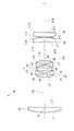
次に、本実施形態に係る顕微鏡装置1に用いられる対物レンズ4の第1実施例について、図2、図3および以下のレンズデータを参照して説明する。
本実施例の対物レンズ4は、図2に示されるように、像側から順に、像側に凸面を有する凸平レンズ41、両凸レンズと両凹レンズとの接合レンズ42、コーデッドアパーチャ5を構成する平板ガラス、両凹レンズと両凸レンズとの接合レンズ43、像側に平面を有する平凸レンズ44および像側に凸面を有する凸平レンズ45により構成されている。Next, a first embodiment of the
As shown in FIG. 2, the
面番号 r d nd νd
1 25.0153 2.0000 1.7380 32.26
2 292.9546 12.6145
3 10.3060 1.3797 1.6779 55.34
4 −15.2096 0.5500 1.7380 32.26
5 6.9967 1.0000
6 ∞ 1.0000 1.4585 67.80
7 ∞ 1.0000
8 −8.2426 0.5500 1.7380 32.26
9 9.1210 1.3985 1.6779 55.34
10 −11.8561 7.7073
11 340.5246 2.0000 1.7410 52.64
12 −16.0238 0.1000
13 18.7919 2.0000 1.8040 46.58
14 2582.3521 12.0000Surface number r d nd ν d
1 25.0153 2.0000 1.7380 32.26
2 292.95446 12.6145
3 10.3060 1.3977 1.6779 55.34
4-15.2096 0.5500 1.7380 32.26
5 6.99667 1.0000
6 ∞ 1.0000 1.4585 67.80
7 ∞ 1.000
8-8.2426 0.5500 1.7380 32.26
9 9.1210 1.3985 1.6779 55.34
10-11.8561 7.7073
11 340.5246 2.0000 1.7410 52.64
12-16.0238 0.1000
13 18.7919 2.0000 1.8040 46.58
14 2582.3521 12.0000
対物レンズ4の焦点距離:20mm、開口数:0.25である。
上記レンズデータにおいて、面番号7がコーデッドアパーチャ5であり、曲率半径rは∞と標記しているが、実際の形状は、
z=2.29×10⁻¹¹(x3+y3) (3)
である。ここで、
zは光軸方向、
x,yは光軸に直交する方向
であり、単位はμmである。The focal length of the
In the above lens data, the
z = 2.29 × 10⁻¹¹ (x 3 + y 3 ) (3)
Is. here,
z is the optical axis direction,
x and y are directions orthogonal to the optical axis, and the unit is μm.
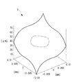
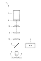
コーデッドアパーチャ5の形状を図3に示す。図中、線で囲まれた領域は、有効径領域である。
平板ガラスの材質は合成石英または他の自家蛍光の少ないガラス材である。
対物レンズ4は物体側テレセントリックであり、コーデッドアパーチャ5は主光線が光軸と交わる瞳位置近傍に配置されている。
このレンズデータによれば、コーデッドアパーチャ5は条件式(1)、(2)を満足している。The shape of the coded
The material of the flat glass is synthetic quartz or other glass material with low autofluorescence.
The
According to this lens data, the coded
次に、本実施形態に係る顕微鏡装置1に用いられる対物レンズ4の第2実施例について、図4以下のレンズデータを参照して説明する。
本実施例の対物レンズ4は、図4に示されるように、像側から順に、像側に凸面を有する凸凹レンズ51、像側に平面を有する平凹レンズ52、像側に凹面を有する2つのメニスカスレンズの接合レンズ53、両凹レンズと両凸レンズとの接合レンズ54、両凸レンズとメニスカスレンズとの接合レンズ55、コーデッドアパーチャ5を構成する平板ガラス、像側に凸面を有する2つのメニスカスレンズと両凸レンズとの接合レンズ56、像側に凸面を有するメニスカスレンズ57、像側に凸面を有するメニスカスレンズ58および平板ガラス59により構成されている。Next, a second embodiment of the
As shown in FIG. 4, the
面番号 r d nd νd
S1 9.4856 4.0021 1.7380 32.26
S2 44.6040 1.3826
S3 123.6400 1.5550 1.5163 64.14
S4 5.2208 4.2338
S5 −5.1821 1.0629 1.7380 32.26
S6 −14.4055 5.0923 1.5952 67.74
S7 −7.7045 0.1000
S8 −20.3293 0.7064 1.6730 38.15
S9 18.3759 4.5922 1.4388 94.95
S10 −13.5171 3.5332
S11 18.3274 6.2265 1.4388 94.95
S12 −8.5895 1.8470 1.6378 42.41
S13 −111.9647 0.1474
S14 ∞ 1.0000 1.4585 67.80
S15 ∞ 0.1474
S16 12.8936 3.6828 1.4388 94.95
S17 111.3686 0.7424 1.6378 42.41
S18 9.3695 6.7753 1.4388 94.95
S19 −15.2624 0.1000
S20 6.8341 4.2468 1.8040 46.58
S21 8.5535 0.1229
S22 3.4561 3.5247 1.8830 40.77
S23 1.4000 0.4000 1.4585 67.80
S24 ∞ 0.3200 1.4041 51.90
S25 ∞ 0.1700 1.4585 67.80Surface number r d nd ν d
S1 9.4856 4.0021 1.7380 32.26
S2 44.6040 1.3826
S3 123.6400 1.5550 1.5163 64.14
S4 5.2208 4.2338
S5-5.1821 1.0629 1.7380 32.26
S6-14.4055 5.0923 1.5952 67.74
S7-7.7045 0.1000
S8-20.3293 0.7064 1.6730 38.15
S9 18.3759 4.5922 1.4388 94.95
S10 -13.5171 3.5332
S11 18.3274 6.2265 1.4388 94.95
S12-8.5895 1.8470 1.6378 42.41
S13-111.9647 0.1474
S14 ∞ 1.0000 1.4585 67.80
S15 ∞ 0.1474
S16 12.8936 3.6828 1.4388 94.95
S17 111.3686 0.7424 1.6378 42.41
S18 9.3695 6.7753 1.4388 94.95
S19-15.26224 0.1000
S20 6.8341 4.2468 1.8040 46.58
S21 8.5535 0.1229
S22 3.4561 3.5247 1.8830 40.77
S23 1.4000 0.4000 1.4585 67.80
S24 ∞ 0.3200 1.4041 51.90
S25 ∞ 0.1700 1.4585 67.80
対物レンズ4の焦点距離:4.5mm、開口数:1.25である。
上記レンズデータにおいて、面番号15がコーデッドアパーチャ5であり、曲率半径rは∞と標記しているが、実際の形状は、式(3)および図3の通りである。The focal length of the
In the above lens data, the surface number 15 is the coded
平板ガラスの材質は合成石英または他の自家蛍光の少ないガラス材である。
対物レンズ4は物体側テレセントリックであり、コーデッドアパーチャ5は主光線が光軸と交わる瞳位置近傍に配置されている。
このレンズデータによれば、コーデッドアパーチャ5は条件式(1)、(2)を満足している。The material of the flat glass is synthetic quartz or other glass material with low autofluorescence.
The
According to this lens data, the coded
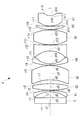
次に、本実施形態に係る顕微鏡装置1に用いられる対物レンズ4の第3実施例について、図5および以下のレンズデータを参照して説明する。
本実施例の対物レンズ4は、図5に示されるように、像側から順に、コーデッドアパーチャ5を構成する平板ガラス、像側に凹面を有するメニスカスレンズ61、両凸レンズ62、像側に凹面を有するメニスカスレンズ63、像側に凸面を有するメニスカスレンズと両凸レンズと両凹レンズとの接合レンズ64、両凸レンズ65、像側に凸面を有するメニスカスレンズ66および像側に凸面を有するメニスカスレンズ67により構成されている。Next, a third embodiment of the
As shown in FIG. 5, the
面番号 r d nd νd
S1 ∞ 2.0000 1.5163 64.14
S2 ∞ 2.0000
S3 −8.5000 0.4600 1.5163 64.14
S4 −17.7969 0.1000
S5 25.9886 2.1310 1.7380 32.26
S6 −26.8723 1.3536
S7 −13.3818 4.8626 1.4970 81.55
S8 −11.6780 0.1000
S9 18.3631 0.4600 1.6730 38.15
S10 6.5862 4.3664 1.4970 81.55
S11 −7.0381 1.9931 1.6730 38.15
S12 57.3994 0.1173
S13 12.2679 5.0000 1.4388 94.95
S14 −14.8618 0.1000
S15 11.1001 1.1271 1.6779 55.34
S16 34.2081 0.1000
S17 6.1519 3.5138 1.8830 40.77
S18 3.5000 2.5005Surface number r d nd ν d
S1 ∞ 2.0000 1.5163 64.14
S2 ∞ 2.0000
S3-8.5000 0.4600 1.5163 64.14
S4-17.7969 0.1000
S5 25.9886 2.1310 1.7380 32.26
S6-26.8723 1.3536
S7-13.3818 4.8626 1.4970 81.55
S8 -11.6780 0.1000
S9 18.3631 0.4600 1.6730 38.15
S10 6.5862 4.3664 1.4970 81.55
S11-7.0381 1.9931 1.6730 38.15
S12 57.3994 0.1173
S13 12.2679 5.0000 1.4388 94.95
S14-14.8618 0.1000
S15 11.1001 1.1271 1.6779 55.34
S16 34.2081 0.1000
S17 6.1519 3.5138 1.8830 40.77
S18 3.5000 2,50005
対物レンズ4の焦点距離:9mm、開口数:0.5である。
上記レンズデータにおいて、面番号2がコーデッドアパーチャ5であり、曲率半径rは∞と標記しているが、実際の形状は、式(3)および図3の通りである。The focal length of the
In the above lens data, the
平板ガラスの材質は合成石英または他の自家蛍光の少ないガラス材である。
対物レンズ4は物体側テレセントリックであり、コーデッドアパーチャ5は主光線が光軸と交わる瞳位置近傍に配置されている。
このレンズデータによれば、コーデッドアパーチャ5は条件式(1)、(2)を満足している。The material of the flat glass is synthetic quartz or other glass material with low autofluorescence.
The
According to this lens data, the coded
なお、本実施形態においては、コーデッドアパーチャ5を対物レンズ4の瞳位置に配置することにより、顕微鏡装置1をコンパクトに構成することができ、かつ、合成石英の選択により紫外光による迷光の発生を抑えている。これに代えて、図6に示されるように、ダイクロイックミラー8と撮像素子7との間に、対物レンズ4の瞳をリレーするリレーレンズ10を配置し、リレーレンズ10によって構成された瞳と光学的に共役な位置にコーデッドアパーチャ5を配置してもよい。
In the present embodiment, the microscope device 1 can be compactly configured by arranging the coded
これによっても、短時間に標本Xの3次元蛍光像を取得することができる。
この場合には、リレーレンズ10およびコーデッドアパーチャ5を配置するためのスペースを確保する必要があるが、コーデッドアパーチャ5に励起光を通過させずに済むので、より多くの種類のガラス材から選択することができるという利点がある。This also makes it possible to obtain a three-dimensional fluorescence image of the sample X in a short time.
In this case, it is necessary to secure a space for arranging the
また、本実施形態においては、対物レンズ4を経由して標本Xに励起光を照射し、かつ、対物レンズ4によって蛍光を集光する、いわゆる、落射照明方式の顕微鏡装置1を例に挙げて説明したが、これに代えて、励起光は、対物レンズ4を経由せずに標本Xに照射してもよい。その場合には、対物レンズ4の瞳位置にコーデッドアパーチャ5を配置しつつ、コーデッドアパーチャ5を構成する平板ガラスを、より多くの種類のガラス材から選択することができる。
Further, in the present embodiment, a so-called epi-illumination type microscope device 1 in which the specimen X is irradiated with excitation light via the
また、本実施形態においては、撮像素子7の撮像面にマイクロレンズアレイ9を配置して、ライトフィールド技術を利用する顕微鏡装置1を例示したが、マイクロレンズアレイ9はなくてもよい。コーデッドアパーチャ5による深度拡大効果によって、標本Xの3次元情報を取得することができる。また、本実施形態においては、顕微鏡装置1は、ライトフィールド技術およびコーデッドアパーチャ技術の少なくとも一方を用いて画像処理を実行する画像処理部を備えていてもよい。
Further, in the present embodiment, the microscope device 1 in which the
1 顕微鏡装置
2 ステージ
3 光源
4 対物レンズ
5 コーデッドアパーチャ(位相板)
6 結像レンズ
7 撮像素子
8 ダイクロイックミラー
9 マイクロレンズアレイ
X 標本1
6
Claims (9)
該ステージに載置された前記標本に励起光が照射されることにより該標本において発生した蛍光を集光する対物レンズと、
該対物レンズにより集光された蛍光を透過させる位相板と、
該位相板を透過した蛍光を集光する結像レンズと、
該結像レンズにより集光された前記標本の蛍光像を撮影する撮像素子とを備え、
前記位相板が、前記対物レンズの瞳位置または該瞳位置と光学的に共役な位置に配置されている顕微鏡装置。The stage on which the specimen is placed and
An objective lens that collects the fluorescence generated in the specimen by irradiating the specimen placed on the stage with excitation light.
A phase plate that transmits the fluorescence collected by the objective lens and
An imaging lens that collects fluorescence transmitted through the phase plate and
It is provided with an image pickup element that captures a fluorescence image of the sample collected by the imaging lens.
A microscope device in which the phase plate is arranged at the pupil position of the objective lens or at a position optically conjugate with the pupil position.
前記位相板の材質が下記の条件式を満たす請求項4に記載の顕微鏡装置。
1.43≦nd≦1.61
62≦νd≦95
ここで、ndはd線における屈折率、νdはd線におけるアッベ数である。The excitation light is ultraviolet light,
The microscope device according to claim 4, wherein the material of the phase plate satisfies the following conditional expression.
1.43 ≤ nd ≤ 1.61
62 ≤ ν d ≤ 95
Here, nd is the refractive index on the d line, and νd is the Abbe number on the d line.
z=k(x3+y3)
ここで、zは光軸方向、x,yは前記光軸に直交し、かつ相互に直交する2方向の座標、kは任意の有理数である。The microscope device according to any one of claims 1 to 5, wherein the shape of the phase plate is represented by the following formula.
z = k (x 3 + y 3 )
Here, z is the optical axis direction, x and y are coordinates in two directions orthogonal to the optical axis and orthogonal to each other, and k is an arbitrary rational number.
該光源からの前記励起光が入射するダイクロイックミラーと、
該ダイクロイックミラーよりも標本側に配置され、前記ダイクロイックミラーによって反射された前記励起光を前記標本に集光する対物レンズと、
前記ダイクロイックミラーよりも前記標本側、かつ前記対物レンズの瞳位置または該瞳位置と光学的に共役な位置に配置され、前記ダイクロイックミラーによって反射された前記励起光が入射する位相板と、
前記標本に前記励起光が照射されることによって発生した蛍光を集光する結像レンズと、
該結像レンズによって集光された前記標本の蛍光像を撮影する撮像素子とを備え、
前記標本に前記励起光が照射されることによって発生した前記蛍光が、前記対物レンズおよび前記位相板を通過してから前記ダイクロイックミラーに入射し、該ダイクロイックミラーを透過した前記蛍光を前記結像レンズによって集光することにより前記標本の蛍光像を前記撮像素子上に結像する顕微鏡装置。A light source that emits excitation light and
A dichroic mirror into which the excitation light from the light source is incident,
An objective lens arranged on the specimen side of the dichroic mirror and condensing the excitation light reflected by the dichroic mirror on the specimen.
A phase plate arranged on the specimen side of the dichroic mirror and at a position optically coupled to the pupil position or the pupil position of the objective lens and to which the excitation light reflected by the dichroic mirror is incident.
An imaging lens that collects the fluorescence generated by irradiating the specimen with the excitation light, and
It is provided with an image pickup element that captures a fluorescence image of the sample collected by the imaging lens.
The fluorescence generated by irradiating the sample with the excitation light passes through the objective lens and the phase plate and then enters the dichroic mirror, and the fluorescence transmitted through the dichroic mirror is transmitted to the imaging lens. A microscope device that forms a fluorescent image of the sample on the image pickup element by condensing the light.
Applications Claiming Priority (1)
| Application Number | Priority Date | Filing Date | Title |
|---|---|---|---|
| PCT/JP2018/027954 WO2020021663A1 (en) | 2018-07-25 | 2018-07-25 | Microscope device |
Publications (1)
| Publication Number | Publication Date |
|---|---|
| JPWO2020021663A1 true JPWO2020021663A1 (en) | 2021-08-02 |
Family
ID=69182245
Family Applications (1)
| Application Number | Title | Priority Date | Filing Date |
|---|---|---|---|
| JP2020531900A Pending JPWO2020021663A1 (en) | 2018-07-25 | 2018-07-25 | Microscope device |
Country Status (4)
| Country | Link |
|---|---|
| US (1) | US20210141202A1 (en) |
| JP (1) | JPWO2020021663A1 (en) |
| CN (1) | CN112437895A (en) |
| WO (1) | WO2020021663A1 (en) |
Families Citing this family (6)
| Publication number | Priority date | Publication date | Assignee | Title |
|---|---|---|---|---|
| WO2020021662A1 (en) * | 2018-07-25 | 2020-01-30 | オリンパス株式会社 | Microscope objective lens and microscope |
| CN115605576B (en) * | 2020-06-10 | 2025-06-06 | 深圳华大生命科学研究院 | Biological sample image acquisition device and gene sequencer |
| CN113253435B (en) * | 2021-07-08 | 2021-09-21 | 深圳市海创光学有限公司 | Coaxial telecentric lens system |
| CN114894113B (en) * | 2022-04-27 | 2024-01-12 | 山东大学 | Material surface layer removal in-situ measurement device and method based on fluorescence tracking sample points |
| CN115278007A (en) * | 2022-07-11 | 2022-11-01 | Oppo广东移动通信有限公司 | Image acquisition method, terminal and readable storage medium |
| CN115379116A (en) * | 2022-08-15 | 2022-11-22 | Oppo广东移动通信有限公司 | Image acquisition method, electronic device, and computer-readable storage medium |
Citations (6)
| Publication number | Priority date | Publication date | Assignee | Title |
|---|---|---|---|---|
| JPS62297879A (en) * | 1986-06-18 | 1987-12-25 | Nec Corp | Producing device for phase shifted diffraction grating |
| JPH09179034A (en) * | 1995-12-26 | 1997-07-11 | Olympus Optical Co Ltd | Top-light fluorescence microscope |
| JP2004318181A (en) * | 1993-05-17 | 2004-11-11 | Olympus Corp | Inverted microscope |
| WO2008047893A1 (en) * | 2006-10-19 | 2008-04-24 | Olympus Corporation | Microscope |
| JP2015210470A (en) * | 2014-04-30 | 2015-11-24 | オリンパス株式会社 | Microscope device |
| US20160062100A1 (en) * | 2014-08-26 | 2016-03-03 | The Board Of Trustees Of The Leland Stanford Junior University | Light-field microscopy with phase masking |
Family Cites Families (6)
| Publication number | Priority date | Publication date | Assignee | Title |
|---|---|---|---|---|
| JP3647062B2 (en) * | 1993-05-17 | 2005-05-11 | オリンパス株式会社 | Upright microscope |
| EP2118699B1 (en) * | 2006-11-06 | 2018-09-12 | University of Massachusetts | Systems and methods of all-optical fourier phase contrast imaging using dye doped liquid crystals |
| WO2011135819A1 (en) * | 2010-04-26 | 2011-11-03 | 株式会社ニコン | Structural illumination microscope device |
| CN105209956B (en) * | 2013-04-30 | 2017-10-24 | 奥林巴斯株式会社 | Sample observes device and sample observational technique |
| JP6299409B2 (en) * | 2014-05-14 | 2018-03-28 | ソニー株式会社 | Phase contrast microscope and phase contrast microscope system |
| US9952422B2 (en) * | 2016-01-14 | 2018-04-24 | University Of Vienna | Enhancing the resolution of three dimensional video images formed using a light field microscope |
-
2018
- 2018-07-25 JP JP2020531900A patent/JPWO2020021663A1/en active Pending
- 2018-07-25 WO PCT/JP2018/027954 patent/WO2020021663A1/en not_active Ceased
- 2018-07-25 CN CN201880095744.2A patent/CN112437895A/en active Pending
-
2021
- 2021-01-22 US US17/155,345 patent/US20210141202A1/en not_active Abandoned
Patent Citations (6)
| Publication number | Priority date | Publication date | Assignee | Title |
|---|---|---|---|---|
| JPS62297879A (en) * | 1986-06-18 | 1987-12-25 | Nec Corp | Producing device for phase shifted diffraction grating |
| JP2004318181A (en) * | 1993-05-17 | 2004-11-11 | Olympus Corp | Inverted microscope |
| JPH09179034A (en) * | 1995-12-26 | 1997-07-11 | Olympus Optical Co Ltd | Top-light fluorescence microscope |
| WO2008047893A1 (en) * | 2006-10-19 | 2008-04-24 | Olympus Corporation | Microscope |
| JP2015210470A (en) * | 2014-04-30 | 2015-11-24 | オリンパス株式会社 | Microscope device |
| US20160062100A1 (en) * | 2014-08-26 | 2016-03-03 | The Board Of Trustees Of The Leland Stanford Junior University | Light-field microscopy with phase masking |
Non-Patent Citations (1)
| Title |
|---|
| NOY COHEN: "Enhancing the performance of the light field microscope using wavefront coding", OPTICS EXTRESS, vol. 22, no. 20, JPN7022000451, 6 October 2014 (2014-10-06), pages 24817 - 24839, ISSN: 0004926003 * |
Also Published As
| Publication number | Publication date |
|---|---|
| CN112437895A (en) | 2021-03-02 |
| WO2020021663A1 (en) | 2020-01-30 |
| US20210141202A1 (en) | 2021-05-13 |
Similar Documents
| Publication | Publication Date | Title |
|---|---|---|
| JPWO2020021663A1 (en) | Microscope device | |
| US10108008B2 (en) | Image-forming optical system, illumination apparatus, and observation apparatus | |
| JP5287252B2 (en) | Laser scanning confocal microscope | |
| JP6847693B2 (en) | Lighting equipment and microscope equipment | |
| JP2005316068A (en) | Optical system | |
| JP5286774B2 (en) | Microscope device and fluorescent cube used therefor | |
| JP2006154230A (en) | Zoom microscope | |
| US10649191B2 (en) | Specimen observation apparatus and specimen observation method | |
| JP4939806B2 (en) | Laser scanning fluorescence microscope | |
| CN112703440A (en) | Microscope system | |
| JP5655617B2 (en) | microscope | |
| US7304282B2 (en) | Focus detection device and fluorescent observation device using the same | |
| US20210165201A1 (en) | Microscope objective lens and microscope | |
| JP2004317749A (en) | Objective | |
| JP6367690B2 (en) | Scanning microscope | |
| JP6829527B2 (en) | A device for imaging a sample and its method | |
| JP2010032622A (en) | Observation device | |
| JP4454980B2 (en) | Microscope imaging optical system and microscope using the same | |
| JP4862368B2 (en) | Zoom microscope | |
| CN113892042B (en) | Apparatus, systems and methods for solid immersion meniscus lenses | |
| JP2013148651A (en) | Microscope | |
| JP3144513B2 (en) | Fluorescence microscope | |
| JP2007293210A (en) | Imaging device | |
| EP3627205A1 (en) | Confocal laser scanning microscope configured for generating line foci | |
| JP2013200438A (en) | microscope |
Legal Events
| Date | Code | Title | Description |
|---|---|---|---|
| A621 | Written request for application examination |
Free format text: JAPANESE INTERMEDIATE CODE: A621 Effective date: 20210119 |
|
| A131 | Notification of reasons for refusal |
Free format text: JAPANESE INTERMEDIATE CODE: A131 Effective date: 20220202 |
|
| A521 | Request for written amendment filed |
Free format text: JAPANESE INTERMEDIATE CODE: A523 Effective date: 20220330 |
|
| A131 | Notification of reasons for refusal |
Free format text: JAPANESE INTERMEDIATE CODE: A131 Effective date: 20220531 |
|
| A02 | Decision of refusal |
Free format text: JAPANESE INTERMEDIATE CODE: A02 Effective date: 20221122 |