JPWO2019066079A1 - Manufacturing method of laminate with protective film and laminate with protective film - Google Patents
Manufacturing method of laminate with protective film and laminate with protective film Download PDFInfo
- Publication number
- JPWO2019066079A1 JPWO2019066079A1 JP2019545205A JP2019545205A JPWO2019066079A1 JP WO2019066079 A1 JPWO2019066079 A1 JP WO2019066079A1 JP 2019545205 A JP2019545205 A JP 2019545205A JP 2019545205 A JP2019545205 A JP 2019545205A JP WO2019066079 A1 JPWO2019066079 A1 JP WO2019066079A1
- Authority
- JP
- Japan
- Prior art keywords
- protective film
- laminate
- resin layer
- resin
- layer
- Prior art date
- Legal status (The legal status is an assumption and is not a legal conclusion. Google has not performed a legal analysis and makes no representation as to the accuracy of the status listed.)
- Granted
Links
- 230000001681 protective effect Effects 0.000 title claims abstract description 425
- 238000004519 manufacturing process Methods 0.000 title claims abstract description 26
- 229920005989 resin Polymers 0.000 claims abstract description 457
- 239000011347 resin Substances 0.000 claims abstract description 457
- 150000001875 compounds Chemical class 0.000 claims abstract description 148
- 239000000463 material Substances 0.000 claims abstract description 147
- 239000000203 mixture Substances 0.000 claims abstract description 88
- 238000000576 coating method Methods 0.000 claims abstract description 75
- 239000011248 coating agent Substances 0.000 claims abstract description 74
- 238000000034 method Methods 0.000 claims abstract description 63
- 238000007373 indentation Methods 0.000 claims abstract description 55
- 230000005865 ionizing radiation Effects 0.000 claims abstract description 54
- 230000004224 protection Effects 0.000 claims abstract description 16
- 230000008569 process Effects 0.000 claims abstract description 10
- 230000001678 irradiating effect Effects 0.000 claims abstract description 5
- 239000010410 layer Substances 0.000 claims description 480
- 239000000835 fiber Substances 0.000 claims description 300
- 239000002346 layers by function Substances 0.000 claims description 183
- 238000010438 heat treatment Methods 0.000 claims description 102
- 229920001296 polysiloxane Polymers 0.000 claims description 59
- 125000002947 alkylene group Chemical group 0.000 claims description 37
- XLYOFNOQVPJJNP-UHFFFAOYSA-N water Substances O XLYOFNOQVPJJNP-UHFFFAOYSA-N 0.000 claims description 27
- 239000011342 resin composition Substances 0.000 claims description 4
- 238000003475 lamination Methods 0.000 claims description 2
- 238000001035 drying Methods 0.000 abstract description 9
- 230000005855 radiation Effects 0.000 abstract 1
- 239000010408 film Substances 0.000 description 599
- 239000000047 product Substances 0.000 description 90
- 238000005259 measurement Methods 0.000 description 77
- BQCADISMDOOEFD-UHFFFAOYSA-N Silver Chemical compound [Ag] BQCADISMDOOEFD-UHFFFAOYSA-N 0.000 description 75
- 239000000523 sample Substances 0.000 description 55
- 239000007788 liquid Substances 0.000 description 48
- 229910052751 metal Inorganic materials 0.000 description 48
- 239000002184 metal Substances 0.000 description 48
- 239000002245 particle Substances 0.000 description 41
- 239000002042 Silver nanowire Substances 0.000 description 34
- 239000012790 adhesive layer Substances 0.000 description 33
- 229920000139 polyethylene terephthalate Polymers 0.000 description 32
- 239000005020 polyethylene terephthalate Substances 0.000 description 32
- NIXOWILDQLNWCW-UHFFFAOYSA-M Acrylate Chemical compound [O-]C(=O)C=C NIXOWILDQLNWCW-UHFFFAOYSA-M 0.000 description 30
- LYCAIKOWRPUZTN-UHFFFAOYSA-N Ethylene glycol Chemical compound OCCO LYCAIKOWRPUZTN-UHFFFAOYSA-N 0.000 description 30
- 239000011521 glass Substances 0.000 description 29
- -1 polyethylene Polymers 0.000 description 29
- PXHVJJICTQNCMI-UHFFFAOYSA-N nickel Substances [Ni] PXHVJJICTQNCMI-UHFFFAOYSA-N 0.000 description 28
- 206010040844 Skin exfoliation Diseases 0.000 description 26
- YCKRFDGAMUMZLT-UHFFFAOYSA-N Fluorine atom Chemical compound [F] YCKRFDGAMUMZLT-UHFFFAOYSA-N 0.000 description 25
- 239000011737 fluorine Substances 0.000 description 25
- 229910052731 fluorine Inorganic materials 0.000 description 25
- 230000000052 comparative effect Effects 0.000 description 24
- VYPSYNLAJGMNEJ-UHFFFAOYSA-N Silicium dioxide Chemical compound O=[Si]=O VYPSYNLAJGMNEJ-UHFFFAOYSA-N 0.000 description 23
- 239000003505 polymerization initiator Substances 0.000 description 23
- 239000006185 dispersion Substances 0.000 description 22
- 125000000524 functional group Chemical group 0.000 description 21
- NTIZESTWPVYFNL-UHFFFAOYSA-N Methyl isobutyl ketone Chemical compound CC(C)CC(C)=O NTIZESTWPVYFNL-UHFFFAOYSA-N 0.000 description 20
- UIHCLUNTQKBZGK-UHFFFAOYSA-N Methyl isobutyl ketone Natural products CCC(C)C(C)=O UIHCLUNTQKBZGK-UHFFFAOYSA-N 0.000 description 20
- 230000005540 biological transmission Effects 0.000 description 20
- 238000002834 transmittance Methods 0.000 description 19
- ZWEHNKRNPOVVGH-UHFFFAOYSA-N 2-Butanone Chemical compound CCC(C)=O ZWEHNKRNPOVVGH-UHFFFAOYSA-N 0.000 description 18
- 238000006073 displacement reaction Methods 0.000 description 18
- 239000010954 inorganic particle Substances 0.000 description 18
- 238000001556 precipitation Methods 0.000 description 17
- LFQSCWFLJHTTHZ-UHFFFAOYSA-N Ethanol Chemical compound CCO LFQSCWFLJHTTHZ-UHFFFAOYSA-N 0.000 description 16
- 230000008859 change Effects 0.000 description 16
- 238000005516 engineering process Methods 0.000 description 16
- 239000000126 substance Substances 0.000 description 16
- 239000002216 antistatic agent Substances 0.000 description 13
- 239000007864 aqueous solution Substances 0.000 description 13
- 239000002657 fibrous material Substances 0.000 description 13
- 229910052709 silver Inorganic materials 0.000 description 13
- 239000000243 solution Substances 0.000 description 13
- 239000002904 solvent Substances 0.000 description 13
- HVVWZTWDBSEWIH-UHFFFAOYSA-N [2-(hydroxymethyl)-3-prop-2-enoyloxy-2-(prop-2-enoyloxymethyl)propyl] prop-2-enoate Chemical compound C=CC(=O)OCC(CO)(COC(=O)C=C)COC(=O)C=C HVVWZTWDBSEWIH-UHFFFAOYSA-N 0.000 description 12
- 239000002612 dispersion medium Substances 0.000 description 12
- 239000004332 silver Substances 0.000 description 12
- 238000012360 testing method Methods 0.000 description 12
- OKTJSMMVPCPJKN-UHFFFAOYSA-N Carbon Chemical compound [C] OKTJSMMVPCPJKN-UHFFFAOYSA-N 0.000 description 11
- 239000011324 bead Substances 0.000 description 11
- 238000006243 chemical reaction Methods 0.000 description 11
- 229940043265 methyl isobutyl ketone Drugs 0.000 description 11
- 239000002070 nanowire Substances 0.000 description 11
- 238000012545 processing Methods 0.000 description 11
- 239000004840 adhesive resin Substances 0.000 description 10
- 229920006223 adhesive resin Polymers 0.000 description 10
- SQGYOTSLMSWVJD-UHFFFAOYSA-N silver(1+) nitrate Chemical compound [Ag+].[O-]N(=O)=O SQGYOTSLMSWVJD-UHFFFAOYSA-N 0.000 description 10
- 239000007787 solid Substances 0.000 description 10
- MYWOJODOMFBVCB-UHFFFAOYSA-N 1,2,6-trimethylphenanthrene Chemical compound CC1=CC=C2C3=CC(C)=CC=C3C=CC2=C1C MYWOJODOMFBVCB-UHFFFAOYSA-N 0.000 description 9
- CSCPPACGZOOCGX-UHFFFAOYSA-N Acetone Chemical compound CC(C)=O CSCPPACGZOOCGX-UHFFFAOYSA-N 0.000 description 9
- 229920002284 Cellulose triacetate Polymers 0.000 description 9
- NNLVGZFZQQXQNW-ADJNRHBOSA-N [(2r,3r,4s,5r,6s)-4,5-diacetyloxy-3-[(2s,3r,4s,5r,6r)-3,4,5-triacetyloxy-6-(acetyloxymethyl)oxan-2-yl]oxy-6-[(2r,3r,4s,5r,6s)-4,5,6-triacetyloxy-2-(acetyloxymethyl)oxan-3-yl]oxyoxan-2-yl]methyl acetate Chemical compound O([C@@H]1O[C@@H]([C@H]([C@H](OC(C)=O)[C@H]1OC(C)=O)O[C@H]1[C@@H]([C@@H](OC(C)=O)[C@H](OC(C)=O)[C@@H](COC(C)=O)O1)OC(C)=O)COC(=O)C)[C@@H]1[C@@H](COC(C)=O)O[C@@H](OC(C)=O)[C@H](OC(C)=O)[C@H]1OC(C)=O NNLVGZFZQQXQNW-ADJNRHBOSA-N 0.000 description 9
- 239000010949 copper Substances 0.000 description 9
- 238000010586 diagram Methods 0.000 description 9
- 229910052759 nickel Inorganic materials 0.000 description 9
- 229920001721 polyimide Polymers 0.000 description 9
- 125000003118 aryl group Chemical group 0.000 description 8
- 230000001588 bifunctional effect Effects 0.000 description 8
- 230000000704 physical effect Effects 0.000 description 8
- 229920005992 thermoplastic resin Polymers 0.000 description 8
- FHLPGTXWCFQMIU-UHFFFAOYSA-N [4-[2-(4-prop-2-enoyloxyphenyl)propan-2-yl]phenyl] prop-2-enoate Chemical class C=1C=C(OC(=O)C=C)C=CC=1C(C)(C)C1=CC=C(OC(=O)C=C)C=C1 FHLPGTXWCFQMIU-UHFFFAOYSA-N 0.000 description 7
- 239000000654 additive Substances 0.000 description 7
- 229910052799 carbon Inorganic materials 0.000 description 7
- 239000003795 chemical substances by application Substances 0.000 description 7
- 238000005520 cutting process Methods 0.000 description 7
- 239000010931 gold Substances 0.000 description 7
- 238000000059 patterning Methods 0.000 description 7
- 229920001225 polyester resin Polymers 0.000 description 7
- 239000009719 polyimide resin Substances 0.000 description 7
- 229920000036 polyvinylpyrrolidone Polymers 0.000 description 7
- 235000013855 polyvinylpyrrolidone Nutrition 0.000 description 7
- 239000000758 substrate Substances 0.000 description 7
- 239000004593 Epoxy Substances 0.000 description 6
- XEKOWRVHYACXOJ-UHFFFAOYSA-N Ethyl acetate Chemical compound CCOC(C)=O XEKOWRVHYACXOJ-UHFFFAOYSA-N 0.000 description 6
- OKKJLVBELUTLKV-UHFFFAOYSA-N Methanol Chemical compound OC OKKJLVBELUTLKV-UHFFFAOYSA-N 0.000 description 6
- ZMXDDKWLCZADIW-UHFFFAOYSA-N N,N-Dimethylformamide Chemical compound CN(C)C=O ZMXDDKWLCZADIW-UHFFFAOYSA-N 0.000 description 6
- WHNWPMSKXPGLAX-UHFFFAOYSA-N N-Vinyl-2-pyrrolidone Chemical compound C=CN1CCCC1=O WHNWPMSKXPGLAX-UHFFFAOYSA-N 0.000 description 6
- HEMHJVSKTPXQMS-UHFFFAOYSA-M Sodium hydroxide Chemical compound [OH-].[Na+] HEMHJVSKTPXQMS-UHFFFAOYSA-M 0.000 description 6
- PPBRXRYQALVLMV-UHFFFAOYSA-N Styrene Chemical compound C=CC1=CC=CC=C1 PPBRXRYQALVLMV-UHFFFAOYSA-N 0.000 description 6
- YXFVVABEGXRONW-UHFFFAOYSA-N Toluene Chemical compound CC1=CC=CC=C1 YXFVVABEGXRONW-UHFFFAOYSA-N 0.000 description 6
- 230000001133 acceleration Effects 0.000 description 6
- 229910052782 aluminium Inorganic materials 0.000 description 6
- 229910017052 cobalt Inorganic materials 0.000 description 6
- 239000010941 cobalt Substances 0.000 description 6
- GUTLYIVDDKVIGB-UHFFFAOYSA-N cobalt atom Chemical compound [Co] GUTLYIVDDKVIGB-UHFFFAOYSA-N 0.000 description 6
- 239000012141 concentrate Substances 0.000 description 6
- 229910052802 copper Inorganic materials 0.000 description 6
- VLKZOEOYAKHREP-UHFFFAOYSA-N n-Hexane Chemical compound CCCCCC VLKZOEOYAKHREP-UHFFFAOYSA-N 0.000 description 6
- 230000003287 optical effect Effects 0.000 description 6
- 229920002647 polyamide Polymers 0.000 description 6
- 229920000642 polymer Polymers 0.000 description 6
- 229920005672 polyolefin resin Polymers 0.000 description 6
- NIXOWILDQLNWCW-UHFFFAOYSA-N 2-Propenoic acid Natural products OC(=O)C=C NIXOWILDQLNWCW-UHFFFAOYSA-N 0.000 description 5
- RYGMFSIKBFXOCR-UHFFFAOYSA-N Copper Chemical compound [Cu] RYGMFSIKBFXOCR-UHFFFAOYSA-N 0.000 description 5
- IAYPIBMASNFSPL-UHFFFAOYSA-N Ethylene oxide Chemical compound C1CO1 IAYPIBMASNFSPL-UHFFFAOYSA-N 0.000 description 5
- KFZMGEQAYNKOFK-UHFFFAOYSA-N Isopropanol Chemical compound CC(C)O KFZMGEQAYNKOFK-UHFFFAOYSA-N 0.000 description 5
- 239000006087 Silane Coupling Agent Substances 0.000 description 5
- WYURNTSHIVDZCO-UHFFFAOYSA-N Tetrahydrofuran Chemical compound C1CCOC1 WYURNTSHIVDZCO-UHFFFAOYSA-N 0.000 description 5
- XAGFODPZIPBFFR-UHFFFAOYSA-N aluminium Chemical compound [Al] XAGFODPZIPBFFR-UHFFFAOYSA-N 0.000 description 5
- 239000002041 carbon nanotube Substances 0.000 description 5
- 229910021393 carbon nanotube Inorganic materials 0.000 description 5
- 229920002678 cellulose Polymers 0.000 description 5
- 238000004043 dyeing Methods 0.000 description 5
- 238000010894 electron beam technology Methods 0.000 description 5
- 229910052737 gold Inorganic materials 0.000 description 5
- 238000003384 imaging method Methods 0.000 description 5
- 239000004973 liquid crystal related substance Substances 0.000 description 5
- 239000011146 organic particle Substances 0.000 description 5
- 229920003023 plastic Polymers 0.000 description 5
- 239000004033 plastic Substances 0.000 description 5
- BASFCYQUMIYNBI-UHFFFAOYSA-N platinum Substances [Pt] BASFCYQUMIYNBI-UHFFFAOYSA-N 0.000 description 5
- 229920000515 polycarbonate Polymers 0.000 description 5
- 239000004417 polycarbonate Substances 0.000 description 5
- 239000004645 polyester resin Substances 0.000 description 5
- 229920005862 polyol Polymers 0.000 description 5
- 238000002360 preparation method Methods 0.000 description 5
- 230000002265 prevention Effects 0.000 description 5
- 229910001961 silver nitrate Inorganic materials 0.000 description 5
- 238000003756 stirring Methods 0.000 description 5
- 230000037303 wrinkles Effects 0.000 description 5
- 229920000178 Acrylic resin Polymers 0.000 description 4
- 239000004925 Acrylic resin Substances 0.000 description 4
- 229920000049 Carbon (fiber) Polymers 0.000 description 4
- LRHPLDYGYMQRHN-UHFFFAOYSA-N N-Butanol Chemical compound CCCCO LRHPLDYGYMQRHN-UHFFFAOYSA-N 0.000 description 4
- 239000004952 Polyamide Substances 0.000 description 4
- 239000004962 Polyamide-imide Substances 0.000 description 4
- GOOHAUXETOMSMM-UHFFFAOYSA-N Propylene oxide Chemical compound CC1CO1 GOOHAUXETOMSMM-UHFFFAOYSA-N 0.000 description 4
- 229910018879 Pt—Pd Inorganic materials 0.000 description 4
- 239000002313 adhesive film Substances 0.000 description 4
- 229910045601 alloy Inorganic materials 0.000 description 4
- 239000000956 alloy Substances 0.000 description 4
- 230000015572 biosynthetic process Effects 0.000 description 4
- 238000012662 bulk polymerization Methods 0.000 description 4
- 239000004917 carbon fiber Substances 0.000 description 4
- 239000001913 cellulose Substances 0.000 description 4
- 238000005336 cracking Methods 0.000 description 4
- JHIVVAPYMSGYDF-UHFFFAOYSA-N cyclohexanone Chemical compound O=C1CCCCC1 JHIVVAPYMSGYDF-UHFFFAOYSA-N 0.000 description 4
- 230000001066 destructive effect Effects 0.000 description 4
- 239000000428 dust Substances 0.000 description 4
- 150000002222 fluorine compounds Chemical class 0.000 description 4
- 239000012528 membrane Substances 0.000 description 4
- 239000000178 monomer Substances 0.000 description 4
- 230000006911 nucleation Effects 0.000 description 4
- 238000010899 nucleation Methods 0.000 description 4
- 229910052697 platinum Inorganic materials 0.000 description 4
- 229920002312 polyamide-imide Polymers 0.000 description 4
- 239000011164 primary particle Substances 0.000 description 4
- 238000011160 research Methods 0.000 description 4
- 239000012798 spherical particle Substances 0.000 description 4
- QTBSBXVTEAMEQO-UHFFFAOYSA-N Acetic acid Chemical compound CC(O)=O QTBSBXVTEAMEQO-UHFFFAOYSA-N 0.000 description 3
- RTZKZFJDLAIYFH-UHFFFAOYSA-N Diethyl ether Chemical compound CCOCC RTZKZFJDLAIYFH-UHFFFAOYSA-N 0.000 description 3
- 239000005977 Ethylene Substances 0.000 description 3
- WSFSSNUMVMOOMR-UHFFFAOYSA-N Formaldehyde Chemical compound O=C WSFSSNUMVMOOMR-UHFFFAOYSA-N 0.000 description 3
- PEDCQBHIVMGVHV-UHFFFAOYSA-N Glycerine Chemical compound OCC(O)CO PEDCQBHIVMGVHV-UHFFFAOYSA-N 0.000 description 3
- KWYUFKZDYYNOTN-UHFFFAOYSA-M Potassium hydroxide Chemical compound [OH-].[K+] KWYUFKZDYYNOTN-UHFFFAOYSA-M 0.000 description 3
- 125000003647 acryloyl group Chemical group O=C([*])C([H])=C([H])[H] 0.000 description 3
- 239000000853 adhesive Substances 0.000 description 3
- 230000001070 adhesive effect Effects 0.000 description 3
- 150000001298 alcohols Chemical class 0.000 description 3
- 238000004364 calculation method Methods 0.000 description 3
- 125000004432 carbon atom Chemical group C* 0.000 description 3
- 239000004020 conductor Substances 0.000 description 3
- 229920001577 copolymer Polymers 0.000 description 3
- 230000007547 defect Effects 0.000 description 3
- 235000014113 dietary fatty acids Nutrition 0.000 description 3
- MTHSVFCYNBDYFN-UHFFFAOYSA-N diethylene glycol Chemical compound OCCOCCO MTHSVFCYNBDYFN-UHFFFAOYSA-N 0.000 description 3
- BXKDSDJJOVIHMX-UHFFFAOYSA-N edrophonium chloride Chemical compound [Cl-].CC[N+](C)(C)C1=CC=CC(O)=C1 BXKDSDJJOVIHMX-UHFFFAOYSA-N 0.000 description 3
- 150000002148 esters Chemical class 0.000 description 3
- 238000011156 evaluation Methods 0.000 description 3
- 239000000194 fatty acid Substances 0.000 description 3
- 229930195729 fatty acid Natural products 0.000 description 3
- 239000005357 flat glass Substances 0.000 description 3
- PCHJSUWPFVWCPO-UHFFFAOYSA-N gold Chemical compound [Au] PCHJSUWPFVWCPO-UHFFFAOYSA-N 0.000 description 3
- XEEYBQQBJWHFJM-UHFFFAOYSA-N iron Substances [Fe] XEEYBQQBJWHFJM-UHFFFAOYSA-N 0.000 description 3
- 239000000314 lubricant Substances 0.000 description 3
- QSHDDOUJBYECFT-UHFFFAOYSA-N mercury Chemical compound [Hg] QSHDDOUJBYECFT-UHFFFAOYSA-N 0.000 description 3
- 229910052753 mercury Inorganic materials 0.000 description 3
- 150000002739 metals Chemical class 0.000 description 3
- 239000012044 organic layer Substances 0.000 description 3
- 229910000489 osmium tetroxide Inorganic materials 0.000 description 3
- 239000012285 osmium tetroxide Substances 0.000 description 3
- KDLHZDBZIXYQEI-UHFFFAOYSA-N palladium Substances [Pd] KDLHZDBZIXYQEI-UHFFFAOYSA-N 0.000 description 3
- WXZMFSXDPGVJKK-UHFFFAOYSA-N pentaerythritol Chemical compound OCC(CO)(CO)CO WXZMFSXDPGVJKK-UHFFFAOYSA-N 0.000 description 3
- IYDGMDWEHDFVQI-UHFFFAOYSA-N phosphoric acid;trioxotungsten Chemical compound O=[W](=O)=O.O=[W](=O)=O.O=[W](=O)=O.O=[W](=O)=O.O=[W](=O)=O.O=[W](=O)=O.O=[W](=O)=O.O=[W](=O)=O.O=[W](=O)=O.O=[W](=O)=O.O=[W](=O)=O.O=[W](=O)=O.OP(O)(O)=O IYDGMDWEHDFVQI-UHFFFAOYSA-N 0.000 description 3
- 238000000206 photolithography Methods 0.000 description 3
- 229920006122 polyamide resin Polymers 0.000 description 3
- 230000000379 polymerizing effect Effects 0.000 description 3
- 229910001927 ruthenium tetroxide Inorganic materials 0.000 description 3
- 239000002356 single layer Substances 0.000 description 3
- 238000004544 sputter deposition Methods 0.000 description 3
- 229910052714 tellurium Inorganic materials 0.000 description 3
- PORWMNRCUJJQNO-UHFFFAOYSA-N tellurium atom Chemical compound [Te] PORWMNRCUJJQNO-UHFFFAOYSA-N 0.000 description 3
- 239000010936 titanium Substances 0.000 description 3
- 229910052719 titanium Inorganic materials 0.000 description 3
- RYHBNJHYFVUHQT-UHFFFAOYSA-N 1,4-Dioxane Chemical compound C1COCCO1 RYHBNJHYFVUHQT-UHFFFAOYSA-N 0.000 description 2
- ARXJGSRGQADJSQ-UHFFFAOYSA-N 1-methoxypropan-2-ol Chemical compound COCC(C)O ARXJGSRGQADJSQ-UHFFFAOYSA-N 0.000 description 2
- TXBCBTDQIULDIA-UHFFFAOYSA-N 2-[[3-hydroxy-2,2-bis(hydroxymethyl)propoxy]methyl]-2-(hydroxymethyl)propane-1,3-diol Chemical compound OCC(CO)(CO)COCC(CO)(CO)CO TXBCBTDQIULDIA-UHFFFAOYSA-N 0.000 description 2
- GZVHEAJQGPRDLQ-UHFFFAOYSA-N 6-phenyl-1,3,5-triazine-2,4-diamine Chemical compound NC1=NC(N)=NC(C=2C=CC=CC=2)=N1 GZVHEAJQGPRDLQ-UHFFFAOYSA-N 0.000 description 2
- 229920002799 BoPET Polymers 0.000 description 2
- KAKZBPTYRLMSJV-UHFFFAOYSA-N Butadiene Chemical compound C=CC=C KAKZBPTYRLMSJV-UHFFFAOYSA-N 0.000 description 2
- DKPFZGUDAPQIHT-UHFFFAOYSA-N Butyl acetate Natural products CCCCOC(C)=O DKPFZGUDAPQIHT-UHFFFAOYSA-N 0.000 description 2
- 229920000298 Cellophane Polymers 0.000 description 2
- VEXZGXHMUGYJMC-UHFFFAOYSA-M Chloride anion Chemical compound [Cl-] VEXZGXHMUGYJMC-UHFFFAOYSA-M 0.000 description 2
- IAZDPXIOMUYVGZ-UHFFFAOYSA-N Dimethylsulphoxide Chemical compound CS(C)=O IAZDPXIOMUYVGZ-UHFFFAOYSA-N 0.000 description 2
- VGGSQFUCUMXWEO-UHFFFAOYSA-N Ethene Chemical compound C=C VGGSQFUCUMXWEO-UHFFFAOYSA-N 0.000 description 2
- JOYRKODLDBILNP-UHFFFAOYSA-N Ethyl urethane Chemical compound CCOC(N)=O JOYRKODLDBILNP-UHFFFAOYSA-N 0.000 description 2
- VEXZGXHMUGYJMC-UHFFFAOYSA-N Hydrochloric acid Chemical compound Cl VEXZGXHMUGYJMC-UHFFFAOYSA-N 0.000 description 2
- 229920000877 Melamine resin Polymers 0.000 description 2
- FXHOOIRPVKKKFG-UHFFFAOYSA-N N,N-Dimethylacetamide Chemical compound CN(C)C(C)=O FXHOOIRPVKKKFG-UHFFFAOYSA-N 0.000 description 2
- SECXISVLQFMRJM-UHFFFAOYSA-N N-Methylpyrrolidone Chemical compound CN1CCCC1=O SECXISVLQFMRJM-UHFFFAOYSA-N 0.000 description 2
- CTQNGGLPUBDAKN-UHFFFAOYSA-N O-Xylene Chemical compound CC1=CC=CC=C1C CTQNGGLPUBDAKN-UHFFFAOYSA-N 0.000 description 2
- 239000004696 Poly ether ether ketone Substances 0.000 description 2
- 229920001609 Poly(3,4-ethylenedioxythiophene) Polymers 0.000 description 2
- 239000004698 Polyethylene Substances 0.000 description 2
- 239000004642 Polyimide Substances 0.000 description 2
- 239000004793 Polystyrene Substances 0.000 description 2
- QAOWNCQODCNURD-UHFFFAOYSA-N Sulfuric acid Chemical compound OS(O)(=O)=O QAOWNCQODCNURD-UHFFFAOYSA-N 0.000 description 2
- KKEYFWRCBNTPAC-UHFFFAOYSA-N Terephthalic acid Chemical compound OC(=O)C1=CC=C(C(O)=O)C=C1 KKEYFWRCBNTPAC-UHFFFAOYSA-N 0.000 description 2
- DKGAVHZHDRPRBM-UHFFFAOYSA-N Tert-Butanol Chemical compound CC(C)(C)O DKGAVHZHDRPRBM-UHFFFAOYSA-N 0.000 description 2
- GWEVSGVZZGPLCZ-UHFFFAOYSA-N Titan oxide Chemical compound O=[Ti]=O GWEVSGVZZGPLCZ-UHFFFAOYSA-N 0.000 description 2
- RTAQQCXQSZGOHL-UHFFFAOYSA-N Titanium Chemical compound [Ti] RTAQQCXQSZGOHL-UHFFFAOYSA-N 0.000 description 2
- XTXRWKRVRITETP-UHFFFAOYSA-N Vinyl acetate Chemical compound CC(=O)OC=C XTXRWKRVRITETP-UHFFFAOYSA-N 0.000 description 2
- XLOMVQKBTHCTTD-UHFFFAOYSA-N Zinc monoxide Chemical compound [Zn]=O XLOMVQKBTHCTTD-UHFFFAOYSA-N 0.000 description 2
- 239000006096 absorbing agent Substances 0.000 description 2
- XECAHXYUAAWDEL-UHFFFAOYSA-N acrylonitrile butadiene styrene Chemical compound C=CC=C.C=CC#N.C=CC1=CC=CC=C1 XECAHXYUAAWDEL-UHFFFAOYSA-N 0.000 description 2
- 229920000122 acrylonitrile butadiene styrene Polymers 0.000 description 2
- 239000004676 acrylonitrile butadiene styrene Substances 0.000 description 2
- 230000000996 additive effect Effects 0.000 description 2
- 125000002723 alicyclic group Chemical group 0.000 description 2
- 125000001931 aliphatic group Chemical group 0.000 description 2
- 239000004760 aramid Substances 0.000 description 2
- 150000004945 aromatic hydrocarbons Chemical class 0.000 description 2
- 229920003235 aromatic polyamide Polymers 0.000 description 2
- 239000011230 binding agent Substances 0.000 description 2
- IISBACLAFKSPIT-UHFFFAOYSA-N bisphenol A Chemical compound C=1C=C(O)C=CC=1C(C)(C)C1=CC=C(O)C=C1 IISBACLAFKSPIT-UHFFFAOYSA-N 0.000 description 2
- WERYXYBDKMZEQL-UHFFFAOYSA-N butane-1,4-diol Chemical compound OCCCCO WERYXYBDKMZEQL-UHFFFAOYSA-N 0.000 description 2
- 238000004140 cleaning Methods 0.000 description 2
- 238000001246 colloidal dispersion Methods 0.000 description 2
- 239000003086 colorant Substances 0.000 description 2
- 238000010276 construction Methods 0.000 description 2
- 239000013078 crystal Substances 0.000 description 2
- 125000004122 cyclic group Chemical group 0.000 description 2
- SWXVUIWOUIDPGS-UHFFFAOYSA-N diacetone alcohol Chemical compound CC(=O)CC(C)(C)O SWXVUIWOUIDPGS-UHFFFAOYSA-N 0.000 description 2
- 229920005994 diacetyl cellulose Polymers 0.000 description 2
- 239000002270 dispersing agent Substances 0.000 description 2
- 239000000975 dye Substances 0.000 description 2
- 239000003822 epoxy resin Substances 0.000 description 2
- 150000002170 ethers Chemical class 0.000 description 2
- 125000001495 ethyl group Chemical group [H]C([H])([H])C([H])([H])* 0.000 description 2
- 150000004665 fatty acids Chemical class 0.000 description 2
- 239000010419 fine particle Substances 0.000 description 2
- 239000005350 fused silica glass Substances 0.000 description 2
- FUZZWVXGSFPDMH-UHFFFAOYSA-M hexanoate Chemical compound CCCCCC([O-])=O FUZZWVXGSFPDMH-UHFFFAOYSA-M 0.000 description 2
- 125000002887 hydroxy group Chemical group [H]O* 0.000 description 2
- 239000003112 inhibitor Substances 0.000 description 2
- 229910052742 iron Inorganic materials 0.000 description 2
- ZFSLODLOARCGLH-UHFFFAOYSA-N isocyanuric acid Chemical compound OC1=NC(O)=NC(O)=N1 ZFSLODLOARCGLH-UHFFFAOYSA-N 0.000 description 2
- 150000002576 ketones Chemical class 0.000 description 2
- JVTAAEKCZFNVCJ-UHFFFAOYSA-N lactic acid Chemical compound CC(O)C(O)=O JVTAAEKCZFNVCJ-UHFFFAOYSA-N 0.000 description 2
- 239000007791 liquid phase Substances 0.000 description 2
- 150000002736 metal compounds Chemical class 0.000 description 2
- 229910021645 metal ion Inorganic materials 0.000 description 2
- 229910044991 metal oxide Inorganic materials 0.000 description 2
- 150000004706 metal oxides Chemical class 0.000 description 2
- VNWKTOKETHGBQD-UHFFFAOYSA-N methane Chemical compound C VNWKTOKETHGBQD-UHFFFAOYSA-N 0.000 description 2
- TZIHFWKZFHZASV-UHFFFAOYSA-N methyl formate Chemical compound COC=O TZIHFWKZFHZASV-UHFFFAOYSA-N 0.000 description 2
- 238000002156 mixing Methods 0.000 description 2
- 239000003960 organic solvent Substances 0.000 description 2
- 230000003647 oxidation Effects 0.000 description 2
- 238000007254 oxidation reaction Methods 0.000 description 2
- 229910052763 palladium Inorganic materials 0.000 description 2
- FDPIMTJIUBPUKL-UHFFFAOYSA-N pentan-3-one Chemical compound CCC(=O)CC FDPIMTJIUBPUKL-UHFFFAOYSA-N 0.000 description 2
- 239000000049 pigment Substances 0.000 description 2
- 238000007747 plating Methods 0.000 description 2
- 229920001643 poly(ether ketone) Polymers 0.000 description 2
- 229920000058 polyacrylate Polymers 0.000 description 2
- 229920000647 polyepoxide Polymers 0.000 description 2
- 229920002530 polyetherether ketone Polymers 0.000 description 2
- 229920000573 polyethylene Polymers 0.000 description 2
- 238000006116 polymerization reaction Methods 0.000 description 2
- 229920000193 polymethacrylate Polymers 0.000 description 2
- 150000003077 polyols Chemical class 0.000 description 2
- 229920002223 polystyrene Polymers 0.000 description 2
- 229920005749 polyurethane resin Polymers 0.000 description 2
- 229920000915 polyvinyl chloride Polymers 0.000 description 2
- 239000004800 polyvinyl chloride Substances 0.000 description 2
- 239000001267 polyvinylpyrrolidone Substances 0.000 description 2
- BDERNNFJNOPAEC-UHFFFAOYSA-N propan-1-ol Chemical compound CCCO BDERNNFJNOPAEC-UHFFFAOYSA-N 0.000 description 2
- 239000003223 protective agent Substances 0.000 description 2
- 230000004044 response Effects 0.000 description 2
- 238000006748 scratching Methods 0.000 description 2
- 230000002393 scratching effect Effects 0.000 description 2
- 239000000377 silicon dioxide Substances 0.000 description 2
- UKLNMMHNWFDKNT-UHFFFAOYSA-M sodium chlorite Chemical compound [Na+].[O-]Cl=O UKLNMMHNWFDKNT-UHFFFAOYSA-M 0.000 description 2
- 229960002218 sodium chlorite Drugs 0.000 description 2
- 229910001220 stainless steel Inorganic materials 0.000 description 2
- 239000010935 stainless steel Substances 0.000 description 2
- 230000003068 static effect Effects 0.000 description 2
- 239000006228 supernatant Substances 0.000 description 2
- 230000001629 suppression Effects 0.000 description 2
- 238000004381 surface treatment Methods 0.000 description 2
- 238000010998 test method Methods 0.000 description 2
- YLQBMQCUIZJEEH-UHFFFAOYSA-N tetrahydrofuran Natural products C=1C=COC=1 YLQBMQCUIZJEEH-UHFFFAOYSA-N 0.000 description 2
- 239000010409 thin film Substances 0.000 description 2
- 229910052718 tin Inorganic materials 0.000 description 2
- 239000011135 tin Substances 0.000 description 2
- XOLBLPGZBRYERU-UHFFFAOYSA-N tin dioxide Chemical compound O=[Sn]=O XOLBLPGZBRYERU-UHFFFAOYSA-N 0.000 description 2
- 229910001887 tin oxide Inorganic materials 0.000 description 2
- 238000000108 ultra-filtration Methods 0.000 description 2
- 238000005406 washing Methods 0.000 description 2
- 238000001039 wet etching Methods 0.000 description 2
- 238000004804 winding Methods 0.000 description 2
- 239000008096 xylene Substances 0.000 description 2
- 229910052725 zinc Inorganic materials 0.000 description 2
- 239000011701 zinc Substances 0.000 description 2
- QNODIIQQMGDSEF-UHFFFAOYSA-N (1-hydroxycyclohexyl)-phenylmethanone Chemical compound C=1C=CC=CC=1C(=O)C1(O)CCCCC1 QNODIIQQMGDSEF-UHFFFAOYSA-N 0.000 description 1
- SCYULBFZEHDVBN-UHFFFAOYSA-N 1,1-Dichloroethane Chemical compound CC(Cl)Cl SCYULBFZEHDVBN-UHFFFAOYSA-N 0.000 description 1
- DHKHKXVYLBGOIT-UHFFFAOYSA-N 1,1-Diethoxyethane Chemical compound CCOC(C)OCC DHKHKXVYLBGOIT-UHFFFAOYSA-N 0.000 description 1
- WSLDOOZREJYCGB-UHFFFAOYSA-N 1,2-Dichloroethane Chemical compound ClCCCl WSLDOOZREJYCGB-UHFFFAOYSA-N 0.000 description 1
- WNXJIVFYUVYPPR-UHFFFAOYSA-N 1,3-dioxolane Chemical compound C1COCO1 WNXJIVFYUVYPPR-UHFFFAOYSA-N 0.000 description 1
- SMZOUWXMTYCWNB-UHFFFAOYSA-N 2-(2-methoxy-5-methylphenyl)ethanamine Chemical compound COC1=CC=C(C)C=C1CCN SMZOUWXMTYCWNB-UHFFFAOYSA-N 0.000 description 1
- XNWFRZJHXBZDAG-UHFFFAOYSA-N 2-METHOXYETHANOL Chemical compound COCCO XNWFRZJHXBZDAG-UHFFFAOYSA-N 0.000 description 1
- PTTPXKJBFFKCEK-UHFFFAOYSA-N 2-Methyl-4-heptanone Chemical compound CC(C)CC(=O)CC(C)C PTTPXKJBFFKCEK-UHFFFAOYSA-N 0.000 description 1
- POAOYUHQDCAZBD-UHFFFAOYSA-N 2-butoxyethanol Chemical compound CCCCOCCO POAOYUHQDCAZBD-UHFFFAOYSA-N 0.000 description 1
- BFSVOASYOCHEOV-UHFFFAOYSA-N 2-diethylaminoethanol Chemical compound CCN(CC)CCO BFSVOASYOCHEOV-UHFFFAOYSA-N 0.000 description 1
- 229940013085 2-diethylaminoethanol Drugs 0.000 description 1
- ZNQVEEAIQZEUHB-UHFFFAOYSA-N 2-ethoxyethanol Chemical compound CCOCCO ZNQVEEAIQZEUHB-UHFFFAOYSA-N 0.000 description 1
- 125000000954 2-hydroxyethyl group Chemical group [H]C([*])([H])C([H])([H])O[H] 0.000 description 1
- 125000003903 2-propenyl group Chemical group [H]C([*])([H])C([H])=C([H])[H] 0.000 description 1
- VPWNQTHUCYMVMZ-UHFFFAOYSA-N 4,4'-sulfonyldiphenol Chemical class C1=CC(O)=CC=C1S(=O)(=O)C1=CC=C(O)C=C1 VPWNQTHUCYMVMZ-UHFFFAOYSA-N 0.000 description 1
- 229920002972 Acrylic fiber Polymers 0.000 description 1
- 239000004953 Aliphatic polyamide Substances 0.000 description 1
- 238000012935 Averaging Methods 0.000 description 1
- 229930185605 Bisphenol Natural products 0.000 description 1
- 229920008347 Cellulose acetate propionate Polymers 0.000 description 1
- VYZAMTAEIAYCRO-UHFFFAOYSA-N Chromium Chemical compound [Cr] VYZAMTAEIAYCRO-UHFFFAOYSA-N 0.000 description 1
- 229910000570 Cupronickel Inorganic materials 0.000 description 1
- 229920000089 Cyclic olefin copolymer Polymers 0.000 description 1
- XDTMQSROBMDMFD-UHFFFAOYSA-N Cyclohexane Chemical compound C1CCCCC1 XDTMQSROBMDMFD-UHFFFAOYSA-N 0.000 description 1
- YZCKVEUIGOORGS-OUBTZVSYSA-N Deuterium Chemical compound [2H] YZCKVEUIGOORGS-OUBTZVSYSA-N 0.000 description 1
- 239000004640 Melamine resin Substances 0.000 description 1
- ZOKXTWBITQBERF-UHFFFAOYSA-N Molybdenum Chemical compound [Mo] ZOKXTWBITQBERF-UHFFFAOYSA-N 0.000 description 1
- 229910021586 Nickel(II) chloride Inorganic materials 0.000 description 1
- 229910019142 PO4 Inorganic materials 0.000 description 1
- 206010034972 Photosensitivity reaction Diseases 0.000 description 1
- 239000004695 Polyether sulfone Substances 0.000 description 1
- 239000004721 Polyphenylene oxide Substances 0.000 description 1
- 239000004743 Polypropylene Substances 0.000 description 1
- 239000004372 Polyvinyl alcohol Substances 0.000 description 1
- XBDQKXXYIPTUBI-UHFFFAOYSA-M Propionate Chemical compound CCC([O-])=O XBDQKXXYIPTUBI-UHFFFAOYSA-M 0.000 description 1
- ATJFFYVFTNAWJD-UHFFFAOYSA-N Tin Chemical compound [Sn] ATJFFYVFTNAWJD-UHFFFAOYSA-N 0.000 description 1
- 230000006750 UV protection Effects 0.000 description 1
- CGQCWMIAEPEHNQ-UHFFFAOYSA-N Vanillylmandelic acid Chemical compound COC1=CC(C(O)C(O)=O)=CC=C1O CGQCWMIAEPEHNQ-UHFFFAOYSA-N 0.000 description 1
- 229920002433 Vinyl chloride-vinyl acetate copolymer Polymers 0.000 description 1
- QYKIQEUNHZKYBP-UHFFFAOYSA-N Vinyl ether Chemical compound C=COC=C QYKIQEUNHZKYBP-UHFFFAOYSA-N 0.000 description 1
- 238000002441 X-ray diffraction Methods 0.000 description 1
- HCHKCACWOHOZIP-UHFFFAOYSA-N Zinc Chemical compound [Zn] HCHKCACWOHOZIP-UHFFFAOYSA-N 0.000 description 1
- SMEGJBVQLJJKKX-HOTMZDKISA-N [(2R,3S,4S,5R,6R)-5-acetyloxy-3,4,6-trihydroxyoxan-2-yl]methyl acetate Chemical compound CC(=O)OC[C@@H]1[C@H]([C@@H]([C@H]([C@@H](O1)O)OC(=O)C)O)O SMEGJBVQLJJKKX-HOTMZDKISA-N 0.000 description 1
- 238000010521 absorption reaction Methods 0.000 description 1
- 239000011354 acetal resin Substances 0.000 description 1
- 125000000218 acetic acid group Chemical group C(C)(=O)* 0.000 description 1
- KXKVLQRXCPHEJC-UHFFFAOYSA-N acetic acid trimethyl ester Natural products COC(C)=O KXKVLQRXCPHEJC-UHFFFAOYSA-N 0.000 description 1
- 229940081735 acetylcellulose Drugs 0.000 description 1
- 125000005396 acrylic acid ester group Chemical group 0.000 description 1
- 238000004220 aggregation Methods 0.000 description 1
- 230000002776 aggregation Effects 0.000 description 1
- 150000001338 aliphatic hydrocarbons Chemical class 0.000 description 1
- 229920003231 aliphatic polyamide Polymers 0.000 description 1
- PNEYBMLMFCGWSK-UHFFFAOYSA-N aluminium oxide Inorganic materials [O-2].[O-2].[O-2].[Al+3].[Al+3] PNEYBMLMFCGWSK-UHFFFAOYSA-N 0.000 description 1
- 150000001408 amides Chemical class 0.000 description 1
- 125000003277 amino group Chemical group 0.000 description 1
- 238000010539 anionic addition polymerization reaction Methods 0.000 description 1
- 238000007743 anodising Methods 0.000 description 1
- 229910052787 antimony Inorganic materials 0.000 description 1
- WATWJIUSRGPENY-UHFFFAOYSA-N antimony atom Chemical compound [Sb] WATWJIUSRGPENY-UHFFFAOYSA-N 0.000 description 1
- 239000003963 antioxidant agent Substances 0.000 description 1
- 238000000149 argon plasma sintering Methods 0.000 description 1
- 239000012298 atmosphere Substances 0.000 description 1
- 238000007611 bar coating method Methods 0.000 description 1
- SYFOAKAXGNMQAX-UHFFFAOYSA-N bis(prop-2-enyl) carbonate;2-(2-hydroxyethoxy)ethanol Chemical compound OCCOCCO.C=CCOC(=O)OCC=C SYFOAKAXGNMQAX-UHFFFAOYSA-N 0.000 description 1
- BTANRVKWQNVYAZ-UHFFFAOYSA-N butan-2-ol Chemical compound CCC(C)O BTANRVKWQNVYAZ-UHFFFAOYSA-N 0.000 description 1
- BPOZNMOEPOHHSC-UHFFFAOYSA-N butyl prop-2-enoate;prop-2-enoic acid Chemical compound OC(=O)C=C.CCCCOC(=O)C=C BPOZNMOEPOHHSC-UHFFFAOYSA-N 0.000 description 1
- 125000003178 carboxy group Chemical group [H]OC(*)=O 0.000 description 1
- 238000010538 cationic polymerization reaction Methods 0.000 description 1
- 229920002301 cellulose acetate Polymers 0.000 description 1
- 229920006217 cellulose acetate butyrate Polymers 0.000 description 1
- 239000003638 chemical reducing agent Substances 0.000 description 1
- VXLPBEHPTWIBJR-UHFFFAOYSA-N chloro tellurohypochlorite Chemical compound Cl[Te]Cl VXLPBEHPTWIBJR-UHFFFAOYSA-N 0.000 description 1
- MVPPADPHJFYWMZ-UHFFFAOYSA-N chlorobenzene Chemical compound ClC1=CC=CC=C1 MVPPADPHJFYWMZ-UHFFFAOYSA-N 0.000 description 1
- 229910052804 chromium Inorganic materials 0.000 description 1
- 239000011651 chromium Substances 0.000 description 1
- 238000004040 coloring Methods 0.000 description 1
- 229920001940 conductive polymer Polymers 0.000 description 1
- YOCUPQPZWBBYIX-UHFFFAOYSA-N copper nickel Chemical compound [Ni].[Cu] YOCUPQPZWBBYIX-UHFFFAOYSA-N 0.000 description 1
- 238000003851 corona treatment Methods 0.000 description 1
- 239000006059 cover glass Substances 0.000 description 1
- 238000004132 cross linking Methods 0.000 description 1
- 150000004292 cyclic ethers Chemical group 0.000 description 1
- CGZZMOTZOONQIA-UHFFFAOYSA-N cycloheptanone Chemical compound O=C1CCCCCC1 CGZZMOTZOONQIA-UHFFFAOYSA-N 0.000 description 1
- 238000010612 desalination reaction Methods 0.000 description 1
- 238000011033 desalting Methods 0.000 description 1
- 238000013461 design Methods 0.000 description 1
- 229910052805 deuterium Inorganic materials 0.000 description 1
- 150000004985 diamines Chemical class 0.000 description 1
- 239000010432 diamond Substances 0.000 description 1
- 229910003460 diamond Inorganic materials 0.000 description 1
- 125000001142 dicarboxylic acid group Chemical group 0.000 description 1
- 238000007607 die coating method Methods 0.000 description 1
- 239000004205 dimethyl polysiloxane Substances 0.000 description 1
- 235000013870 dimethyl polysiloxane Nutrition 0.000 description 1
- 229920001971 elastomer Polymers 0.000 description 1
- 239000000806 elastomer Substances 0.000 description 1
- 230000005611 electricity Effects 0.000 description 1
- 238000007772 electroless plating Methods 0.000 description 1
- 238000009713 electroplating Methods 0.000 description 1
- UHESRSKEBRADOO-UHFFFAOYSA-N ethyl carbamate;prop-2-enoic acid Chemical compound OC(=O)C=C.CCOC(N)=O UHESRSKEBRADOO-UHFFFAOYSA-N 0.000 description 1
- 238000001704 evaporation Methods 0.000 description 1
- 230000001747 exhibiting effect Effects 0.000 description 1
- 238000011049 filling Methods 0.000 description 1
- 239000000706 filtrate Substances 0.000 description 1
- 238000010304 firing Methods 0.000 description 1
- 239000003063 flame retardant Substances 0.000 description 1
- 238000007667 floating Methods 0.000 description 1
- LEXQFRJDSTXIKR-UHFFFAOYSA-N formaldehyde sulfanediol dihydrate Chemical compound O.O.C=O.OSO LEXQFRJDSTXIKR-UHFFFAOYSA-N 0.000 description 1
- 238000007756 gravure coating Methods 0.000 description 1
- 238000009499 grossing Methods 0.000 description 1
- 150000008282 halocarbons Chemical class 0.000 description 1
- 229910052736 halogen Inorganic materials 0.000 description 1
- 150000002367 halogens Chemical class 0.000 description 1
- 238000007542 hardness measurement Methods 0.000 description 1
- 229930195733 hydrocarbon Natural products 0.000 description 1
- 238000007654 immersion Methods 0.000 description 1
- 229910052738 indium Inorganic materials 0.000 description 1
- 230000005764 inhibitory process Effects 0.000 description 1
- 239000003999 initiator Substances 0.000 description 1
- 239000012784 inorganic fiber Substances 0.000 description 1
- 229910010272 inorganic material Inorganic materials 0.000 description 1
- 239000011147 inorganic material Substances 0.000 description 1
- 229910052809 inorganic oxide Inorganic materials 0.000 description 1
- 238000001990 intravenous administration Methods 0.000 description 1
- 229910052741 iridium Inorganic materials 0.000 description 1
- 230000001788 irregular Effects 0.000 description 1
- 239000012948 isocyanate Substances 0.000 description 1
- IQPQWNKOIGAROB-UHFFFAOYSA-N isocyanate group Chemical group [N-]=C=O IQPQWNKOIGAROB-UHFFFAOYSA-N 0.000 description 1
- 239000004310 lactic acid Substances 0.000 description 1
- 235000014655 lactic acid Nutrition 0.000 description 1
- JDSHMPZPIAZGSV-UHFFFAOYSA-N melamine Chemical compound NC1=NC(N)=NC(N)=N1 JDSHMPZPIAZGSV-UHFFFAOYSA-N 0.000 description 1
- 150000007974 melamines Chemical class 0.000 description 1
- 229910001507 metal halide Inorganic materials 0.000 description 1
- 150000005309 metal halides Chemical class 0.000 description 1
- 229910052976 metal sulfide Inorganic materials 0.000 description 1
- 125000002496 methyl group Chemical group [H]C([H])([H])* 0.000 description 1
- 239000011859 microparticle Substances 0.000 description 1
- 238000013508 migration Methods 0.000 description 1
- 230000005012 migration Effects 0.000 description 1
- 238000012986 modification Methods 0.000 description 1
- 230000004048 modification Effects 0.000 description 1
- 239000003607 modifier Substances 0.000 description 1
- 229910052750 molybdenum Inorganic materials 0.000 description 1
- 239000011733 molybdenum Substances 0.000 description 1
- YKYONYBAUNKHLG-UHFFFAOYSA-N n-Propyl acetate Natural products CCCOC(C)=O YKYONYBAUNKHLG-UHFFFAOYSA-N 0.000 description 1
- 239000002105 nanoparticle Substances 0.000 description 1
- QMMRZOWCJAIUJA-UHFFFAOYSA-L nickel dichloride Chemical compound Cl[Ni]Cl QMMRZOWCJAIUJA-UHFFFAOYSA-L 0.000 description 1
- 125000003518 norbornenyl group Chemical group C12(C=CC(CC1)C2)* 0.000 description 1
- 239000012788 optical film Substances 0.000 description 1
- 239000005022 packaging material Substances 0.000 description 1
- 238000010422 painting Methods 0.000 description 1
- 239000012071 phase Substances 0.000 description 1
- 150000002989 phenols Chemical class 0.000 description 1
- WVDDGKGOMKODPV-ZQBYOMGUSA-N phenyl(114C)methanol Chemical compound O[14CH2]C1=CC=CC=C1 WVDDGKGOMKODPV-ZQBYOMGUSA-N 0.000 description 1
- NBIIXXVUZAFLBC-UHFFFAOYSA-K phosphate Chemical compound [O-]P([O-])([O-])=O NBIIXXVUZAFLBC-UHFFFAOYSA-K 0.000 description 1
- 239000010452 phosphate Substances 0.000 description 1
- 230000036211 photosensitivity Effects 0.000 description 1
- 239000004014 plasticizer Substances 0.000 description 1
- 229920000435 poly(dimethylsiloxane) Polymers 0.000 description 1
- 229920003229 poly(methyl methacrylate) Polymers 0.000 description 1
- 229920000636 poly(norbornene) polymer Polymers 0.000 description 1
- 229920000172 poly(styrenesulfonic acid) Polymers 0.000 description 1
- 229920001707 polybutylene terephthalate Polymers 0.000 description 1
- 229920005668 polycarbonate resin Polymers 0.000 description 1
- 239000004431 polycarbonate resin Substances 0.000 description 1
- 229920000728 polyester Polymers 0.000 description 1
- 229920000570 polyether Polymers 0.000 description 1
- 229920006393 polyether sulfone Polymers 0.000 description 1
- 229920001223 polyethylene glycol Polymers 0.000 description 1
- 239000011112 polyethylene naphthalate Substances 0.000 description 1
- 229920013716 polyethylene resin Polymers 0.000 description 1
- 239000012985 polymerization agent Substances 0.000 description 1
- 229920000098 polyolefin Polymers 0.000 description 1
- 229920006324 polyoxymethylene Polymers 0.000 description 1
- 229920001155 polypropylene Polymers 0.000 description 1
- 229940005642 polystyrene sulfonic acid Drugs 0.000 description 1
- 239000005077 polysulfide Substances 0.000 description 1
- 229920001021 polysulfide Polymers 0.000 description 1
- 150000008117 polysulfides Polymers 0.000 description 1
- 229920002689 polyvinyl acetate Polymers 0.000 description 1
- 239000011118 polyvinyl acetate Substances 0.000 description 1
- 229920002451 polyvinyl alcohol Polymers 0.000 description 1
- 229920002102 polyvinyl toluene Polymers 0.000 description 1
- OTYBMLCTZGSZBG-UHFFFAOYSA-L potassium sulfate Chemical compound [K+].[K+].[O-]S([O-])(=O)=O OTYBMLCTZGSZBG-UHFFFAOYSA-L 0.000 description 1
- 229910052939 potassium sulfate Inorganic materials 0.000 description 1
- 235000011151 potassium sulphates Nutrition 0.000 description 1
- 229940090181 propyl acetate Drugs 0.000 description 1
- QQONPFPTGQHPMA-UHFFFAOYSA-N propylene Natural products CC=C QQONPFPTGQHPMA-UHFFFAOYSA-N 0.000 description 1
- 239000011241 protective layer Substances 0.000 description 1
- 239000002096 quantum dot Substances 0.000 description 1
- 150000003242 quaternary ammonium salts Chemical class 0.000 description 1
- 239000007870 radical polymerization initiator Substances 0.000 description 1
- 150000003254 radicals Chemical class 0.000 description 1
- 230000009467 reduction Effects 0.000 description 1
- 230000001846 repelling effect Effects 0.000 description 1
- 230000000717 retained effect Effects 0.000 description 1
- 229910052703 rhodium Inorganic materials 0.000 description 1
- 239000005060 rubber Substances 0.000 description 1
- 238000005070 sampling Methods 0.000 description 1
- 229930195734 saturated hydrocarbon Natural products 0.000 description 1
- 238000007650 screen-printing Methods 0.000 description 1
- 239000004065 semiconductor Substances 0.000 description 1
- 229920002050 silicone resin Polymers 0.000 description 1
- 229920002379 silicone rubber Polymers 0.000 description 1
- 150000003378 silver Chemical class 0.000 description 1
- 239000010944 silver (metal) Substances 0.000 description 1
- 238000007767 slide coating Methods 0.000 description 1
- 239000001488 sodium phosphate Substances 0.000 description 1
- 229910000162 sodium phosphate Inorganic materials 0.000 description 1
- 239000007962 solid dispersion Substances 0.000 description 1
- 230000003595 spectral effect Effects 0.000 description 1
- 238000001228 spectrum Methods 0.000 description 1
- 238000004528 spin coating Methods 0.000 description 1
- 239000007921 spray Substances 0.000 description 1
- 238000005507 spraying Methods 0.000 description 1
- 238000000859 sublimation Methods 0.000 description 1
- 230000008022 sublimation Effects 0.000 description 1
- 150000003462 sulfoxides Chemical class 0.000 description 1
- 238000005987 sulfurization reaction Methods 0.000 description 1
- 239000004094 surface-active agent Substances 0.000 description 1
- 238000003786 synthesis reaction Methods 0.000 description 1
- 229920003051 synthetic elastomer Polymers 0.000 description 1
- 229920002994 synthetic fiber Polymers 0.000 description 1
- 239000012209 synthetic fiber Substances 0.000 description 1
- 239000005061 synthetic rubber Substances 0.000 description 1
- LAJZODKXOMJMPK-UHFFFAOYSA-N tellurium dioxide Chemical compound O=[Te]=O LAJZODKXOMJMPK-UHFFFAOYSA-N 0.000 description 1
- 150000000000 tetracarboxylic acids Chemical class 0.000 description 1
- UWHCKJMYHZGTIT-UHFFFAOYSA-N tetraethylene glycol Chemical compound OCCOCCOCCOCCO UWHCKJMYHZGTIT-UHFFFAOYSA-N 0.000 description 1
- 238000012719 thermal polymerization Methods 0.000 description 1
- 239000002562 thickening agent Substances 0.000 description 1
- 125000003396 thiol group Chemical group [H]S* 0.000 description 1
- 238000012546 transfer Methods 0.000 description 1
- 150000003628 tricarboxylic acids Chemical group 0.000 description 1
- ZIBGPFATKBEMQZ-UHFFFAOYSA-N triethylene glycol Chemical compound OCCOCCOCCO ZIBGPFATKBEMQZ-UHFFFAOYSA-N 0.000 description 1
- SRPWOOOHEPICQU-UHFFFAOYSA-N trimellitic anhydride Chemical group OC(=O)C1=CC=C2C(=O)OC(=O)C2=C1 SRPWOOOHEPICQU-UHFFFAOYSA-N 0.000 description 1
- RYFMWSXOAZQYPI-UHFFFAOYSA-K trisodium phosphate Chemical compound [Na+].[Na+].[Na+].[O-]P([O-])([O-])=O RYFMWSXOAZQYPI-UHFFFAOYSA-K 0.000 description 1
- WFKWXMTUELFFGS-UHFFFAOYSA-N tungsten Chemical compound [W] WFKWXMTUELFFGS-UHFFFAOYSA-N 0.000 description 1
- 229910052721 tungsten Inorganic materials 0.000 description 1
- 239000010937 tungsten Substances 0.000 description 1
- 150000003672 ureas Chemical class 0.000 description 1
- NQPDZGIKBAWPEJ-UHFFFAOYSA-N valeric acid Chemical compound CCCCC(O)=O NQPDZGIKBAWPEJ-UHFFFAOYSA-N 0.000 description 1
- 238000001947 vapour-phase growth Methods 0.000 description 1
- 125000000391 vinyl group Chemical group [H]C([*])=C([H])[H] 0.000 description 1
- 229920002554 vinyl polymer Polymers 0.000 description 1
- 238000003466 welding Methods 0.000 description 1
- 238000005491 wire drawing Methods 0.000 description 1
- 229910052724 xenon Inorganic materials 0.000 description 1
- FHNFHKCVQCLJFQ-UHFFFAOYSA-N xenon atom Chemical compound [Xe] FHNFHKCVQCLJFQ-UHFFFAOYSA-N 0.000 description 1
- 239000011787 zinc oxide Substances 0.000 description 1
Images


Classifications
-
- B—PERFORMING OPERATIONS; TRANSPORTING
- B05—SPRAYING OR ATOMISING IN GENERAL; APPLYING FLUENT MATERIALS TO SURFACES, IN GENERAL
- B05D—PROCESSES FOR APPLYING FLUENT MATERIALS TO SURFACES, IN GENERAL
- B05D5/00—Processes for applying liquids or other fluent materials to surfaces to obtain special surface effects, finishes or structures
-
- B—PERFORMING OPERATIONS; TRANSPORTING
- B05—SPRAYING OR ATOMISING IN GENERAL; APPLYING FLUENT MATERIALS TO SURFACES, IN GENERAL
- B05D—PROCESSES FOR APPLYING FLUENT MATERIALS TO SURFACES, IN GENERAL
- B05D7/00—Processes, other than flocking, specially adapted for applying liquids or other fluent materials to particular surfaces or for applying particular liquids or other fluent materials
- B05D7/24—Processes, other than flocking, specially adapted for applying liquids or other fluent materials to particular surfaces or for applying particular liquids or other fluent materials for applying particular liquids or other fluent materials
-
- B—PERFORMING OPERATIONS; TRANSPORTING
- B32—LAYERED PRODUCTS
- B32B—LAYERED PRODUCTS, i.e. PRODUCTS BUILT-UP OF STRATA OF FLAT OR NON-FLAT, e.g. CELLULAR OR HONEYCOMB, FORM
- B32B27/00—Layered products comprising a layer of synthetic resin
-
- B—PERFORMING OPERATIONS; TRANSPORTING
- B32—LAYERED PRODUCTS
- B32B—LAYERED PRODUCTS, i.e. PRODUCTS BUILT-UP OF STRATA OF FLAT OR NON-FLAT, e.g. CELLULAR OR HONEYCOMB, FORM
- B32B27/00—Layered products comprising a layer of synthetic resin
- B32B27/16—Layered products comprising a layer of synthetic resin specially treated, e.g. irradiated
-
- B—PERFORMING OPERATIONS; TRANSPORTING
- B32—LAYERED PRODUCTS
- B32B—LAYERED PRODUCTS, i.e. PRODUCTS BUILT-UP OF STRATA OF FLAT OR NON-FLAT, e.g. CELLULAR OR HONEYCOMB, FORM
- B32B27/00—Layered products comprising a layer of synthetic resin
- B32B27/30—Layered products comprising a layer of synthetic resin comprising vinyl (co)polymers; comprising acrylic (co)polymers
-
- B—PERFORMING OPERATIONS; TRANSPORTING
- B32—LAYERED PRODUCTS
- B32B—LAYERED PRODUCTS, i.e. PRODUCTS BUILT-UP OF STRATA OF FLAT OR NON-FLAT, e.g. CELLULAR OR HONEYCOMB, FORM
- B32B37/00—Methods or apparatus for laminating, e.g. by curing or by ultrasonic bonding
- B32B37/14—Methods or apparatus for laminating, e.g. by curing or by ultrasonic bonding characterised by the properties of the layers
- B32B37/15—Methods or apparatus for laminating, e.g. by curing or by ultrasonic bonding characterised by the properties of the layers with at least one layer being manufactured and immediately laminated before reaching its stable state, e.g. in which a layer is extruded and laminated while in semi-molten state
-
- B—PERFORMING OPERATIONS; TRANSPORTING
- B32—LAYERED PRODUCTS
- B32B—LAYERED PRODUCTS, i.e. PRODUCTS BUILT-UP OF STRATA OF FLAT OR NON-FLAT, e.g. CELLULAR OR HONEYCOMB, FORM
- B32B7/00—Layered products characterised by the relation between layers; Layered products characterised by the relative orientation of features between layers, or by the relative values of a measurable parameter between layers, i.e. products comprising layers having different physical, chemical or physicochemical properties; Layered products characterised by the interconnection of layers
- B32B7/04—Interconnection of layers
- B32B7/06—Interconnection of layers permitting easy separation
Landscapes
- Life Sciences & Earth Sciences (AREA)
- Engineering & Computer Science (AREA)
- Wood Science & Technology (AREA)
- Laminated Bodies (AREA)
Abstract
本発明の一の態様によれば、第1の基材21と、第1の基材21の一方の面である第1の面21A側に設けられ、かつ膜厚方向Dの断面におけるインデンテーション硬さが100MPa以上の第1の樹脂層22とを備える積層体20を用意する工程と、第2の基材31の一方の面である第1の面31A側に、電離放射線重合性化合物を含む第2の樹脂層用組成物を塗布し、乾燥させて、塗膜35を形成する工程と、第1の樹脂層22が塗膜35に接するように塗膜34に積層体20を接触させる工程と、塗膜35に積層体20を接触させた状態で、塗膜35に電離放射線を照射することにより塗膜35を硬化させて、第2の基材31と、第2の基材31より第1の樹脂層22側に位置し、かつ塗膜35の硬化物からなり、膜厚方向Dの断面におけるインデンテーション硬さが100MPa以上の第2の樹脂層32とを備える剥離可能な保護フィルム30を形成する工程と、を備える、保護フィルム付き積層体10の製造方法が提供される。According to one aspect of the present invention, indentation in a cross section in the film thickness direction D is provided on the first surface 21A side, which is one surface of the first base material 21 and the first base material 21. The step of preparing the laminate 20 including the first resin layer 22 having a hardness of 100 MPa or more, and the ionization radiation polymerizable compound on the first surface 31A side, which is one surface of the second base material 31. The step of applying the composition for the second resin layer containing the mixture and drying it to form the coating film 35, and bringing the laminate 20 into contact with the coating film 34 so that the first resin layer 22 is in contact with the coating film 35. In the process and in the state where the laminate 20 is in contact with the coating film 35, the coating film 35 is cured by irradiating the coating film 35 with ionizing radiation to cure the second base material 31 and the second base material 31. Detachable protection with a second resin layer 32 located closer to the first resin layer 22 and made of a cured product of the coating film 35 and having an indentation hardness of 100 MPa or more in the cross section in the film thickness direction D. Provided is a method for producing a laminate 10 with a protective film, comprising a step of forming the film 30.
Description
本願は、先行する日本国出願である特願2017−191666(出願日:2017年9月29日)の優先権の利益を享受するものであり、その開示内容全体は引用することにより本明細書の一部とされる。 The present application enjoys the priority of the prior application of Japanese Patent Application No. 2017-19166 (Filing date: September 29, 2017), and the entire disclosure thereof is hereby cited by reference. Be part of.
本発明は、保護フィルム付き積層体の製造方法および保護フィルム付き積層体に関する。 The present invention relates to a method for producing a laminate with a protective film and a laminate with a protective film.
従来から、スマートフォンやタブレット端末等の画像表示装置が知られているが、画像表示装置には、基材および基材の一方の面側に設けられたハードコート層を有する積層体が用いられることが多い。 Conventionally, image display devices such as smartphones and tablet terminals have been known, but the image display device uses a base material and a laminate having a hard coat layer provided on one surface side of the base material. There are many.
ハードコート層の表面には、搬送時やその後の加工時において傷が付くことを防止するために、粘着層を有する保護フィルムが貼り付けられている(例えば、特許文献1参照)。この保護フィルムは、搬送や加工等が行われた後、剥離されて、画像表示装置に組み込まれる。 A protective film having an adhesive layer is attached to the surface of the hard coat layer in order to prevent scratches during transportation and subsequent processing (see, for example, Patent Document 1). This protective film is peeled off after being conveyed, processed, or the like, and incorporated into an image display device.
ハードコート層を有する積層体は、センサー(例えば、画像表示装置用途のセンサーや車載用途のセンサー(例えば、ハンドルやシートなど人が触れる部分のセンサーを含む))に用いられることもある。このセンサーは、フォールダブル、ローラブル等のフレキシブル性が必要とされる場合もある。このようなセンサーに用いられる積層体においては、保護フィルムが直前まで貼られているので、保護フィルム付き積層体として、薄型化や両面に多様な機能が要求されている。 The laminate having a hard coat layer may be used for a sensor (for example, a sensor for an image display device or a sensor for an in-vehicle use (for example, a sensor for a part touched by a person such as a handle or a seat)). This sensor may also require flexibility such as foldable and rollable. In the laminate used for such a sensor, since the protective film is attached until just before, the laminate with the protective film is required to be thin and have various functions on both sides.
従来、熱加工工程が行われる保護フィルム付き積層体においては、加工工程前後のカール防止性も求められるので、例えば、保護フィルム付き積層体の表面および裏面には同じ膜厚や同じ樹脂材料を用いることでカール防止性を解決してきた。 Conventionally, in a laminate with a protective film that is subjected to a heat processing process, curl prevention before and after the processing process is also required. This has solved the curl prevention property.
しかしながら、現在、保護フィルム付き積層体の表面と裏面には、異なる機能を持たせることが求められることもあり、異なる樹脂材料を用い、または異なる膜厚にすることが増えてきている。 However, at present, the front surface and the back surface of the laminate with the protective film are required to have different functions, and different resin materials or different film thicknesses are increasingly used.
また、保護フィルムが剥離された積層体を、画像表示装置以外の用途のみならず、画像表示装置の用途にも適用するためには、白濁感のない透明性が求められている。 Further, in order to apply the laminate from which the protective film has been peeled off not only to applications other than image display devices but also to applications of image display devices, transparency without a feeling of cloudiness is required.
さらに、保護フィルムにおいては、積層体を保護するために所定の硬度が求められているとともに、積層体の加工プロセス前後で物性変化が小さいことが求められている。しかしながら、現在の保護フィルムは、粘着層を有するため、保護フィルムの表面において、所定の硬度が得られず、また加工プロセスで積層体の物性が変化してしまうという問題がある。 Further, the protective film is required to have a predetermined hardness in order to protect the laminated body, and is required to have a small change in physical properties before and after the processing process of the laminated body. However, since the current protective film has an adhesive layer, there is a problem that a predetermined hardness cannot be obtained on the surface of the protective film and the physical properties of the laminated body are changed in the processing process.
本発明は、このような点を考慮してなされたものであり、所定の断面硬度や表面硬度を有し、かつ加工プロセス前後での物性変化が小さい保護フィルム付き積層体の製造方法および保護フィルム付き積層体を提供することを目的とする。 The present invention has been made in consideration of these points, and is a method for producing a laminate with a protective film and a protective film having a predetermined cross-sectional hardness and surface hardness and having a small change in physical properties before and after the processing process. It is an object of the present invention to provide a laminated body with a structure.
本発明は、以下の発明を含む。
[1]第1の基材と、前記第1の基材の一方の面側に設けられ、かつ膜厚方向の断面におけるインデンテーション硬さが100MPa以上の第1の樹脂層とを備える積層体を用意する工程と、第2の基材の一方の面側に、電離放射線重合性化合物を含む第2の樹脂層用組成物を塗布し、乾燥させて、塗膜を形成する工程と、前記第1の樹脂層が前記塗膜に接するように前記塗膜に前記積層体を接触させる工程と、前記塗膜に前記積層体を接触させた状態で、前記塗膜に電離放射線を照射することにより前記塗膜を硬化させて、前記第2の基材と、前記第2の基材より前記第1の樹脂層側に位置し、かつ前記塗膜の硬化物からなり、膜厚方向の断面におけるインデンテーション硬さが100MPa以上の第2の樹脂層とを備える剥離可能な保護フィルムを形成する工程と、を備える、保護フィルム付き積層体の製造方法。The present invention includes the following inventions.
[1] A laminated body including a first base material and a first resin layer provided on one surface side of the first base material and having an indentation hardness of 100 MPa or more in a cross section in the film thickness direction. And the step of applying the composition for the second resin layer containing the ionizing radiation polymerizable compound to one surface side of the second base material and drying it to form a coating film. The step of bringing the laminate into contact with the coating film so that the first resin layer is in contact with the coating film, and irradiating the coating film with ionizing radiation in a state where the laminate is in contact with the coating film. The coating film is cured by the above method, and is composed of the second base material, a cured product of the coating film located on the side of the first resin layer from the second base material, and a cross section in the film thickness direction. A method for producing a laminate with a protective film, comprising a step of forming a peelable protective film including a second resin layer having an indentation hardness of 100 MPa or more.
[2]前記第2の樹脂層の前記インデンテーション硬さが、前記第1の樹脂層のインデンテーション硬さよりも小さい、上記[1]に記載の保護フィルム付き積層体の製造方法。 [2] The method for producing a laminate with a protective film according to the above [1], wherein the indentation hardness of the second resin layer is smaller than the indentation hardness of the first resin layer.
[3]前記電離放射線重合性化合物が、アルキレンオキサイド非変性電離放射線重合性化合物と、アルキレンオキサイド変性電離放射線重合性化合物とを含む、上記[1]または[2]に記載の保護フィルム付き積層体の製造方法。 [3] The laminate with a protective film according to the above [1] or [2], wherein the ionizing radiation polymerizable compound contains an alkylene oxide non-modified ionizing radiation polymerizable compound and an alkylene oxide modified ionizing radiation polymerizable compound. Manufacturing method.
[4]前記第2の樹脂層用組成物が、シリコーン系化合物を含む、上記[1]ないし[3]のいずれか一項に記載の保護フィルム付き積層体の製造方法。 [4] The method for producing a laminate with a protective film according to any one of the above [1] to [3], wherein the composition for the second resin layer contains a silicone compound.
[5]第1の基材および前記第1の基材の一方の面側に設けられた第1の樹脂層を備える積層体と、前記積層体に剥離可能に密着した保護フィルムとを備える保護フィルム付き積層体であって、前記保護フィルムが、第2の基材と、前記第2の基材より前記第1の樹脂層側に位置し、かつ前記第1の樹脂層に密着した第2の樹脂層とを備え、前記第1の樹脂層の膜厚方向の断面および前記第2の樹脂層の膜厚方向の断面におけるインデンテーション硬さがそれぞれ100MPa以上である、保護フィルム付き積層体。 [5] Protection including a laminate having a first base material and a first resin layer provided on one surface side of the first base material, and a protective film detachably adhered to the laminate. A second laminate with a film, wherein the protective film is located on the second base material and the first resin layer side of the second base material, and is in close contact with the first resin layer. A laminated body with a protective film, each comprising the above resin layer and having an indentation hardness of 100 MPa or more in the cross section of the first resin layer in the film thickness direction and the cross section of the second resin layer in the film thickness direction.
[6]前記第2の樹脂層の前記インデンテーション硬さが、前記第1の樹脂層のインデンテーション硬さよりも小さい、上記[5]に記載の保護フィルム付き積層体。 [6] The laminate with a protective film according to the above [5], wherein the indentation hardness of the second resin layer is smaller than the indentation hardness of the first resin layer.
[7]前記保護フィルムが、前記第2の基材と前記第2の樹脂層からなる、上記[5]または[6]に記載の保護フィルム付き積層体。 [7] The laminate with a protective film according to the above [5] or [6], wherein the protective film comprises the second base material and the second resin layer.
[8]前記積層体が、前記第1の樹脂層における前記第1の基材側の面とは反対側の面側に設けられた第1の機能層をさらに備え、前記第1の機能層が、光透過性樹脂と、前記光透過性樹脂中に配置された複数の導電性繊維とを含み、前記積層体における前記第1の機能層が存在している領域の拡散光反射率が、0.5%以下である、上記[5]ないし[7]のいずれか一項に記載の保護フィルム付き積層体。 [8] The laminate further includes a first functional layer provided on a surface side of the first resin layer opposite to the surface on the first base material side, and the first functional layer. However, the diffused light reflectance of the region in which the first functional layer is present in the laminate, which contains the light-transmitting resin and the plurality of conductive fibers arranged in the light-transmitting resin, is determined. The laminate with a protective film according to any one of the above [5] to [7], which is 0.5% or less.
[9]前記保護フィルムが、前記第2の基材と前記第2の樹脂層の間に設けられ、または前記第2の基材における前記第2樹脂層側の第1の面とは反対側の第2の面に設けられた第2の機能層をさらに備える、上記[5]ないし[8]に記載の保護フィルム付き積層体。 [9] The protective film is provided between the second base material and the second resin layer, or is on the side opposite to the first surface of the second base material on the second resin layer side. The laminate with a protective film according to the above [5] to [8], further comprising a second functional layer provided on the second surface of the above.
[10]前記第2の樹脂層の膜厚が、1μm以上10μm以下である、上記[5]ないし[9]のいずれか一項に記載の保護フィルム付き積層体。 [10] The laminate with a protective film according to any one of [5] to [9] above, wherein the thickness of the second resin layer is 1 μm or more and 10 μm or less.
[11]前記保護フィルムを剥離した状態での前記第2の樹脂層の表面の鉛筆硬度が、H以上である、上記[5]ないし[10]のいずれか一項に記載の保護フィルム付き積層体。 [11] The laminate with a protective film according to any one of [5] to [10] above, wherein the pencil hardness of the surface of the second resin layer in the state where the protective film is peeled off is H or more. body.
[12]前記保護フィルム付き積層体を150℃の環境下で1時間加熱する前後において、加熱前における前記積層体と前記保護フィルムとの剥離強度および加熱後における前記積層体と前記保護フィルムとの剥離強度をそれぞれ測定したとき、前記加熱前の前記剥離強度に対する前記加熱後における前記剥離強度の上昇率が、100%以下である、上記[5]ないし[11]のいずれか一項に記載の保護フィルム付き積層体。 [12] Before and after heating the laminate with the protective film in an environment of 150 ° C. for 1 hour, the peel strength between the laminate and the protective film before heating and the strength of the laminate and the protective film after heating The item according to any one of [5] to [11] above, wherein when the peel strength is measured, the rate of increase of the peel strength after the heating is 100% or less with respect to the peel strength before the heating. Laminate with protective film.
[13]前記保護フィルム付き積層体を150℃の環境下で1時間加熱した後における前記積層体と前記保護フィルムとの剥離強度が、200mN/25mm以下である、上記[5]ないし[12]のいずれか一項に記載の保護フィルム付き積層体。 [13] The above [5] to [12], wherein the peel strength between the laminate and the protective film after heating the laminate with the protective film in an environment of 150 ° C. for 1 hour is 200 mN / 25 mm or less. The laminate with a protective film according to any one of the above.
[14]前記保護フィルム付き積層体を150℃の環境下で1時間加熱し、加熱後に前記保護フィルムを剥離したときの前記第2の樹脂層の表面における水に対する接触角が、70°以上95°以下である、上記[5]ないし[13]のいずれか一項に記載の保護フィルム付き積層体。 [14] When the laminate with the protective film is heated in an environment of 150 ° C. for 1 hour and the protective film is peeled off after heating, the contact angle with water on the surface of the second resin layer is 70 ° or more and 95 ° C. The laminate with a protective film according to any one of the above [5] to [13], which is less than or equal to °.
[15]前記第2の樹脂層が、アルキレンオキサイド非変性電離放射線重合性化合物と、アルキレンオキサイド変性電離放射線重合性化合物とを含む第2の樹脂用組成物の硬化物である、上記[5]ないし[14]のいずれか一項に記載の保護フィルム付き積層体。 [15] The second resin layer is a cured product of a second resin composition containing an alkylene oxide non-modified ionizing radiation polymerizable compound and an alkylene oxide modified ionizing radiation polymerizable compound. The laminate with a protective film according to any one of [14].
[16]前記第2の樹脂層が、シリコーン系化合物を含む、上記[5]ないし[15]のいずれか一項に記載の保護フィルム付き積層体。 [16] The laminate with a protective film according to any one of [5] to [15] above, wherein the second resin layer contains a silicone compound.
[17]第1の基材および前記第1の基材の一方の面側に設けられた第1の樹脂層を備える積層体と、前記積層体に剥離可能に密着した保護フィルムとを備える保護フィルム付き積層体であって、前記保護フィルムが、第2の基材と、前記第2の基材より前記第1の樹脂層側に位置し、かつ前記第1の樹脂層に密着した第2の樹脂層とを備え、前記保護フィルムを剥離した状態での前記第2の樹脂層の表面の鉛筆硬度が、H以上である、保護フィルム付き積層体。 [17] Protection including a laminate having a first base material and a first resin layer provided on one surface side of the first base material, and a protective film detachably adhered to the laminate. A second laminate with a film, wherein the protective film is located on the second base material and the first resin layer side of the second base material, and is in close contact with the first resin layer. A laminate with a protective film, which comprises the above resin layer and has a pencil hardness of H or more on the surface of the second resin layer in a state where the protective film is peeled off.
[18]第1の基材および前記第1の基材の一方の面側に設けられた第1の樹脂層を備える積層体と、前記積層体に剥離可能に密着した保護フィルムとを備える保護フィルム付き積層体であって、前記保護フィルムが、第2の基材と、前記第2の基材より前記第1の樹脂層側に位置し、かつ前記第1の樹脂層に密着した第2の樹脂層とを備え、前記保護フィルム付き積層体を150℃の環境下で1時間加熱する前後において、加熱前における前記積層体と前記保護フィルムとの剥離強度および加熱後における前記積層体と前記保護フィルムとの剥離強度をそれぞれ測定したとき、前記加熱前の前記剥離強度に対する前記加熱後における前記剥離強度の上昇率が、100%以下である、保護フィルム付き積層体。 [18] Protection including a laminate having a first base material and a first resin layer provided on one surface side of the first base material, and a protective film detachably adhered to the laminate. A second laminate with a film, wherein the protective film is located on the second base material and the first resin layer side of the second base material, and is in close contact with the first resin layer. Before and after heating the laminate with the protective film for 1 hour in an environment of 150 ° C., the peel strength between the laminate and the protective film before heating and the laminate and the laminate after heating are provided. A laminate with a protective film in which the rate of increase in the peel strength after heating is 100% or less with respect to the peel strength before heating, respectively, when the peel strength from the protective film is measured.
[19]第1の基材および前記第1の基材の一方の面側に設けられた第1の樹脂層を備える積層体と、前記積層体に剥離可能に密着した保護フィルムとを備える保護フィルム付き積層体であって、前記保護フィルムが、第2の基材と、前記第2の基材より前記第1の樹脂層側に位置し、かつ前記第1の樹脂層に密着した第2の樹脂層とを備え、前記保護フィルム付き積層体を150℃の環境下で1時間加熱した後における前記積層体と前記保護フィルムとの剥離強度が、200mN/25mm以下である、保護フィルム付き積層体。 [19] Protection including a laminate having a first base material and a first resin layer provided on one surface side of the first base material, and a protective film detachably adhered to the laminate. A second laminate with a film, wherein the protective film is located on the second base material and the first resin layer side of the second base material, and is in close contact with the first resin layer. The peeling strength between the laminate and the protective film after heating the laminate with the protective film in an environment of 150 ° C. for 1 hour is 200 mN / 25 mm or less. body.
[20]第1の基材および前記第1の基材の一方の面側に設けられた第1の樹脂層を備える積層体と、前記積層体に剥離可能に密着した保護フィルムとを備える保護フィルム付き積層体であって、前記保護フィルムが、第2の基材と、前記第2の基材より前記第1の樹脂層側に位置し、かつ前記第1の樹脂層に密着した第2の樹脂層とを備え、前記保護フィルム付き積層体を150℃の環境下で1時間加熱し、加熱後に前記保護フィルムを剥離したときの前記第2の樹脂層の表面における水に対する接触角が、70°以上95°以下である、保護フィルム付き積層体。 [20] Protection including a laminate having a first base material and a first resin layer provided on one surface side of the first base material, and a protective film detachably adhered to the laminate. A second laminate with a film, wherein the protective film is located on the second base material and the first resin layer side of the second base material, and is in close contact with the first resin layer. When the laminate with the protective film is heated in an environment of 150 ° C. for 1 hour and the protective film is peeled off after heating, the contact angle with water on the surface of the second resin layer is determined. A laminate with a protective film that is 70 ° or more and 95 ° or less.
[21]第1の基材および前記第1の基材の一方の面側に設けられた第1の樹脂層を備える積層体と、前記積層体に剥離可能に密着した保護フィルムとを備える保護フィルム付き積層体であって、前記保護フィルムが、第2の基材と、前記第2の基材より前記第1の樹脂層側に位置し、かつ前記第1の樹脂層に密着した第2の樹脂層とを備え、前記第2の樹脂層が、アルキレンオキサイド非変性電離放射線重合性化合物と、アルキレンオキサイド変性電離放射線重合性化合物とを含む第2の樹脂用組成物の硬化物である、保護フィルム付き積層体。 [21] Protection provided with a laminate having a first base material and a first resin layer provided on one surface side of the first base material, and a protective film detachably adhered to the laminate. A second laminate with a film, wherein the protective film is located on the second base material and the first resin layer side of the second base material, and is in close contact with the first resin layer. The second resin layer is a cured product of a second resin composition containing an alkylene oxide non-modified ionizing radiopolymerizable compound and an alkylene oxide modified ionizing radiopolymerizable compound. Laminate with protective film.
本発明によれば、所定の断面硬度や表面硬度を有し、かつ加工プロセス前後での物性変化が小さい保護フィルム付き積層体を提供することができる。 According to the present invention, it is possible to provide a laminate with a protective film having a predetermined cross-sectional hardness and surface hardness and having a small change in physical properties before and after the processing process.
以下、本発明の実施形態に係る積層体、タッチパネル、および画像表示装置について、図面を参照しながら説明する。図1は本実施形態に係る保護フィルム付き積層体の概略構成図であり、図2は図1に示される保護フィルム付き積層体の一部の拡大図である。図3および図4は、実施形態に係る他の保護フィルム付き積層体の概略構成図であり、図5は図4の保護フィルム付き積層体の模式的な平面図である。図6および図7は、実施形態に係る他の保護フィルム付き積層体の概略構成図である。図8(A)〜図8(C)および図9(A)〜図9(C)は本実施形態に係る保護フィルム付き積層体の製造工程を模式的に示した図である。 Hereinafter, the laminate, the touch panel, and the image display device according to the embodiment of the present invention will be described with reference to the drawings. FIG. 1 is a schematic configuration diagram of a laminate with a protective film according to the present embodiment, and FIG. 2 is an enlarged view of a part of the laminate with a protective film shown in FIG. 3 and 4 are schematic configuration views of another laminated body with a protective film according to the embodiment, and FIG. 5 is a schematic plan view of the laminated body with a protective film of FIG. 6 and 7 are schematic configuration views of another laminated body with a protective film according to the embodiment. 8 (A) to 8 (C) and 9 (A) to 9 (C) are diagrams schematically showing the manufacturing process of the laminate with the protective film according to the present embodiment.
<<<<保護フィルム付き積層体>>>>
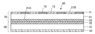
図1に示される保護フィルム付き積層体10は、第1の基材21および第1の基材21の一方の面である第1の面21A側に設けられた第1の樹脂層22を備える積層体20と、積層体20の第1の樹脂層22に剥離可能に密着した保護フィルム30とを備えている。積層体20は、第1の基材21および第1の樹脂層22の他、第1の基材21における第1の面21Aとは反対側の面である第2の面21B側に設けられた第1の機能層23をさらに備えている。本明細書における「機能層」とは、積層体において、何らかの機能を発揮することを意図された層である。具体的には、例えば、積層体における第1の機能層としては、導電層、易接着層、屈折率調整層、弾性・伸びなど物理特性調整層、透過吸収光波長調整層、顔料・染料着色層、紫外線防止層などが挙げられる。機能層は、単層のみならず、2層以上積層されたものであってもよい。機能層が2層以上積層されたものである場合、それぞれの層が有する機能は同じであってもよいが、異なっていてもよい。本実施形態においては、第1の機能層23が、導電層である場合について説明する。<<<< Laminate with protective film >>>>>
The laminate 10 with a protective film shown in FIG. 1 includes a
保護フィルム付き積層体10の厚みは、25μm以上500μm以下であることが好ましい。保護フィルム付き積層体10の厚みが、25μm以上であれば、保護フィルム付き積層体10の搬送時や加工時のハンドリング性が良好となり、また500μm以下であれば、薄型化の観点から良好であり、また容易に巻き取ることができる。保護フィルム付き積層体10の厚みの下限は、50μm以上であることがより好ましく、上限は300μm以下、200μm以下、160μm以下であることがより好ましい(数値が小さいほど好ましい)。保護フィルム付き積層体10の厚みは、厚み測定装置(製品名「デジマチックインジケーターIDF−130」、株式会社ミツトヨ製)を用いて任意の10箇所の厚みを測定し、その算術平均値を算出することにより求めることができる。
The thickness of the
保護フィルム付き積層体10を150℃の環境下で1時間加熱する前後において、加熱前の積層体20と保護フィルム30との剥離強度に対する加熱後の積層体20と保護フィルム30の剥離強度の上昇率は、100%以下であることが好ましい。後述するように、保護フィルム付き積層体を加熱すると、加熱前に比べて積層体と保護フィルムとの剥離強度が上昇してしまう傾向があるが、上記上昇率が、100%以下であれば、保護フィルム付き積層体10を加熱した場合であっても、保護フィルム30を容易に剥離することができる。上記上昇率は、80%以下、60%以下、50%以下、40%以下の順にさらに好ましい(数値が小さいほど好ましい)。なお、上昇率は負であってもよい。加熱前の積層体20と保護フィルム30との剥離強度および加熱後の積層体20と保護フィルム30との剥離強度は、それぞれ、引張り試験機(製品名「テンシロン万能材料試験機RTF−1150−H」、株式会社A&D製)を用い、以下の測定方法により測定される値である。剥離強度の測定の際には、まず、縦12.5cm×横5cm×厚さ1.1mmのガラス板に両面テープ(株式会社寺岡製作所 No.751B)を貼り付ける。一方で、保護フィルム付き積層体を縦15cm×横2.5cmの大きさに切り出し、第1の基材側をガラス板上の両面テープに貼り付け、引張り試験機の一対の治具に保持させる。そして、ガラス板に貼り付けられた保護フィルム付き積層体を引張り試験機の一対の治具に保持させる。治具に保護フィルム付き積層体を保持させる際には、人手で予め積層体から保護フィルムを若干剥離させて、きっかけを作り、片方の治具に保護フィルムを保持させ、他方の治具にガラス板および積層体を保持させる。そして、この状態で、剥離速度300mm/分、剥離距離50mm、剥離角度180°の条件で、保護フィルムを剥離し、そのときの積層体と保護フィルムとの剥離強度を測定する。なお、剥離強度は、3回測定した値の算術平均値とする。加熱前の保護フィルムの剥離強度に対する加熱した後の保護フィルムの剥離強度の上昇率は、前記上昇率をA(%)とし、加熱前の保護フィルムの剥離強度をB(mN/25mm)とし、加熱後の剥離強度をC(mN/25mm)としたとき、以下の式から算出される。なお、上記サンプルの大きさを切り出せない場合には、例えば、縦の長さを8cm程度にすることが可能である。
A=(C−B)/B×100Before and after heating the laminate 10 with a protective film in an environment of 150 ° C. for 1 hour, the peel strength of the laminate 20 and the
A = (CB) / B × 100
保護フィルム付き積層体10を150℃の環境下で1時間加熱する前の積層体20と保護フィルム30との剥離強度は、200mN/25mm以下であることが好ましい。この剥離強度が、200mN/25mm以下であれば、加熱前において、保護フィルム30を容易に剥離することができる。また、保護フィルム付き積層体10を150℃の環境下で1時間した加熱後の積層体20と保護フィルム30との剥離強度は、200mN/25mm以下であることが好ましい。この剥離強度が、200mN/25mm以下であれば、加熱後であっても、保護フィルム30を容易に剥離することができる。加熱前の上記剥離強度および加熱後の上記剥離強度の下限は、保護フィルム30を積層体20に密着させ、有効に第1の樹脂層22を保護する観点から、10mN/25mm以上であることが好ましい。加熱前の上記剥離強度および加熱後の上記剥離強度の上限は、150mN/25mm以下、120mN/25mm以下、110mN/25mm以下、105mN/25mm以下の順にさらに好ましい(数値が小さいほど好ましい)。
The peel strength between the laminate 20 and the
保護フィルム付き積層体10を150℃の環境下で1時間加熱したとき、加熱後の保護フィルム付き積層体10のMD方向およびTD方向の加熱収縮率は、それぞれ、0.8%以下であることが好ましい。ここで、MD方向とは、長方形型ディスプレイである場合は、短軸と平行な方向を、TD方向とは、長軸と平行な方向をいう。正方形である場合には、4辺のうち任意の1辺を選択し、その辺と平行な方向をMD、その辺と垂直な方向をTDという。更に、不定形である場合には、適宜正方形に切り出し(例えば50cm角、40cm角、30cm角、20cm角10cm角、5cm角など可能な大きさの正方形で)前記したような方向をいう。なお、製造工程に用いるロール形態のフィルムにおいては、MDはMachine Direction:機械軸方向(フィルムが流れる進行方向)であり、TDはTransverse Direction:横幅方向である。保護フィルム付き積層体10のMD方向およびTD方向の加熱収縮率が、それぞれ0.8%以下であれば、保護フィルム付き積層体10を加熱した場合に、第1の機能層23がパターニングされていたとしても、第1の機能層23の寸法変化を小さくすることができる。上記MD方向およびTD方向の加熱収縮率は、それぞれ、0.6%以下、0.5%以下の順にさらに好ましい(数値が小さいほど好ましい)。加熱収縮率は、以下のようにして測定するものとする。まず、保護フィルム付き積層体を、MD方向が縦方向となり、TD方向が横方向となるように縦8cm×横8cmの大きさに切り出す。切り出した保護フィルム付き積層体を画像寸法測定器(IM−6120:株式会社キーエンス製)にて加熱前の縦方向および横方向の長さを測定する。そして、この切り出した保護フィルム付き積層体を150℃の環境下で1時間加熱し、加熱後の保護フィルム付き積層体の縦方向および横方向の長さを前記画像寸法測定器にて測定し、以下の式に基づいてMD方向およびTD方向の加熱収縮率を算出する。以下の式においては、DMDはMD方向の加熱収縮率(%)であり、DTDはTD方向の加熱収縮率(%)であり、EMDは加熱前の保護フィルム付き積層体のMD方向の長さ(cm)であり、EMDは加熱前の保護フィルム付き積層体のTD方向の長さ(cm)であり、FMDは加熱後の保護フィルム付き積層体のMD方向の長さ(cm)であり、FMDは加熱後の保護フィルム付き積層体のTD方向の長さ(cm)である。なお、保護フィルム付き積層体を上記大きさに切り出せない場合には、取り扱える可能な大きさである縦2cm×横2cm以上の大きさに保護フィルム付き積層体を適宜切り出してもよい。
DMD=(FMD−EMD)/EMD×100
DTD=(FTD−ETD)/ETD×100When the
D MD = (F MD- E MD ) / E MD x 100
D TD = ( FTD- E TD ) / E TD x 100
保護フィルム付き積層体10を150℃の環境下で1時間加熱したとき、加熱後の保護フィルム付き積層体10のカール量は、±10mm以下であることが好ましい。カール量が±10mm以下であれば、保護フィルム付き積層体10を容易に取り扱うことができる。カール量は、以下のようにして測定するものとする。まず、保護フィルム付き積層体を縦34cm×横34cmの大きさに切り出す。そして、この切り出した保護フィルム付き積層体を150℃の環境下で1時間加熱し、加熱後の保護フィルム付き積層体を平らな台の上に置く。そして、保護フィルム付き積層体の4隅と台との距離をそれぞれ測定し、それを平均した値をカール量とする。なお、台に保護フィルムを下側となるように置いた場合、保護フィルム付き積層体の上面が凹状にカールする場合を正(+)とし、保護フィルム付き積層体の上面が凸状にカールする場合を負(−)とする。カール量は、±9mm以下、±8mm以下、±7mm以下、±5mm以下の順にさらに好ましい(数値が小さいほど好ましい)。なお、保護フィルム付き積層体を上記大きさに切り出せない場合には、カール測定が十分可能な大きさである縦5cm×横5cm以上の大きさに保護フィルム付き積層体を適宜切り出してもよい。
When the laminate 10 with a protective film is heated in an environment of 150 ° C. for 1 hour, the curl amount of the laminate 10 with a protective film after heating is preferably ± 10 mm or less. When the curl amount is ± 10 mm or less, the
保護フィルム付き積層体10を150℃の環境下で1時間加熱する前後において、保護フィルム付き積層体10のヘイズ値(全ヘイズ値)を測定したとき、加熱後の保護フィルム付き積層体10のヘイズ値から加熱前に保護フィルム付き積層体10のヘイズ値を引いた値であるヘイズ変化量は、5%以内であることが好ましい。ヘイズ変化量が、5%以内であれば、加熱後であっても、良好な透明性を有する保護フィルム付き積層体10を得ることができる。このようなヘイズ変化量は、後述する第2の基材31における第2の樹脂層32側の第1の面31Aとは反対側の第2の面31Bにオリゴマー析出抑制層を設けることによって達成することができる。保護フィルム付き積層体10のヘイズ値は、JIS K7136:2000に準拠して、ヘイズメーター(製品名「HM−150」、株式会社村上色彩技術研究所製)を用いて、縦10cm×横10cmの大きさに切り出した後、カールや皺がなく、かつ指紋や埃等がない状態で積層体が非光源側となるように設置し、保護フィルム付き積層体1枚に対して3回測定を行い、3回測定して得られた値の算術平均値とする。保護フィルム付き積層体10は、目視した表面は平坦であり、かつ第1の機能層23等の積層する層も平坦であり、また厚みのばらつきも厚みの平均値の±10%の範囲内、好ましくは±5%の範囲内に収まる。したがって、切り出した保護フィルム付き積層体の異なる3箇所のヘイズ値を測定することで、おおよその保護フィルム付き積層体の面内全体のヘイズ値の平均値が得られると考えられる。なお、保護フィルム付き積層体を上記大きさに切り出せない場合には、例えば、HM−150は測定する際の入口開口が20mmφであるので、直径21mm以上となるような大きさのサンプルが必要になる。このため、22mm×22mm以上の大きさに保護フィルム付き積層体を適宜切り出してもよい。保護フィルム付き積層体の大きさが小さい場合は、光源スポットが外れない範囲で少しずつずらす、または角度を変えるなどして測定点を3箇所にする。保護フィルム付き積層体10においては、得られるヘイズ変化量のばらつきは、測定対象が1m×3000mと長尺であっても、5インチのスマートフォン程度の大きさであっても、ヘイズ値の平均値の±30%以内である。上記ヘイズ変化量は、3%以下、2.5%以下、2%以下、1.7%以下の順にさらに好ましい(数値が小さいほど好ましい)。
When the haze value (total haze value) of the laminate 10 with the protective film is measured before and after heating the laminate 10 with the protective film in an environment of 150 ° C. for 1 hour, the haze of the laminate 10 with the protective film after heating is measured. The amount of change in haze, which is the value obtained by subtracting the haze value of the
保護フィルム付き積層体10の表面10Aの表面抵抗値は、保護フィルム付き積層体10の裏面の表面抵抗値よりも低くなっていてもよい。表面10Aの表面抵抗値は、後述する第1の機能層23の表面抵抗値と同様にして測定することができる。また、裏面10Bの表面抵抗値は、表面抵抗値測定器(製品名「Hiresta IP MCP−HT260」、三菱化学株式会社製)を用いて測定することができる。
The surface resistance value of the
保護フィルム付き積層体から保護フィルムを剥離する際に、剥離帯電するおそれがある。剥離帯電すると、積層体における第1の機能層中の導電性繊維が切れてしまうおそれがある。特に導電性繊維は、細線化の傾向があるので、導電性繊維はより切れやすくなっている。このため、裏面10Bにおける表面抵抗値は、保護フィルム30を剥離したときの剥離帯電および導電性繊維の切れを抑制する観点から、1×10¹³Ω/□以下であることが好ましい。裏面10Bにおけるこのような表面抵抗値は、後述する第2の機能層33に帯電防止剤を含ませることによって、または帯電防止層を形成することによって達成することができる。裏面10Bにおける表面抵抗値は、1×1012Ω/□以下、1×1011Ω/□以下、1×1010Ω/□以下であることがより好ましい(数値が小さいほど好ましい)。When the protective film is peeled off from the laminate with the protective film, there is a risk of peeling charge. When peeling electrification occurs, the conductive fibers in the first functional layer of the laminated body may be cut off. In particular, conductive fibers tend to be thinned, so that the conductive fibers are more easily cut. Therefore, the surface resistance value of the
保護フィルム付き積層体は、所望の大きさにカットされていてもよいが、ロール状であってもよい。保護フィルム付き積層体が所望の大きさにカットされている場合、保護フィルム付き積層体の大きさは、特に制限されず、画像表示装置の表示面の大きさに応じて適宜決定される。具体的には、保護フィルム付き積層体の大きさは、例えば、5インチ以上500インチ以下となっていてもよい。本明細書における「インチ」とは、保護フィルム付き積層体が四角形状である場合には対角線の長さを意味し、円形状である場合には直径を意味し、楕円形状である場合には、短径と長径の和の平均値を意味するものとする。ここで、保護フィルム付き積層体が四角形状である場合、上記インチを求める際の保護フィルム付き積層体の縦横比は、画像表示装置の表示画面として問題がなければ特に限定されない。例えば、縦:横=1:1、4:3、16:10、16:9、2:1等が挙げられる。ただし、特に、デザイン性に富む車載用途やデジタルサイネージにおいては、このような縦横比に限定されない。また、保護フィルム付き積層体10の大きさが大きい場合には、任意の位置(端よりは中央部付近で)からA5サイズ(148mm×210mm)に切り出した後、各測定項目の大きさに切り出すものとする。
The laminate with the protective film may be cut to a desired size, but may be in the form of a roll. When the laminate with the protective film is cut to a desired size, the size of the laminate with the protective film is not particularly limited and is appropriately determined according to the size of the display surface of the image display device. Specifically, the size of the laminate with the protective film may be, for example, 5 inches or more and 500 inches or less. As used herein, the term "inch" means the length of the diagonal line when the laminate with the protective film is square, the diameter when it is circular, and the elliptical shape when it is oval. , It shall mean the average value of the sum of the minor axis and the major axis. Here, when the laminated body with the protective film has a quadrangular shape, the aspect ratio of the laminated body with the protective film when determining the inch is not particularly limited as long as there is no problem in the display screen of the image display device. For example, vertical: horizontal = 1: 1, 4: 3, 16:10, 16: 9, 2: 1 and the like. However, the aspect ratio is not limited to this, especially in in-vehicle applications and digital signage, which are rich in design. When the size of the
<<<積層体>>>
積層体20の厚みは、25μm以上500μm以下であることが好ましい。積層体20の厚みが、25μm以上であれば、ハンドリング性が良好となり、また100μm以下であれば、薄型化の観点から良好である。保護フィルム付き積層体10の厚みの下限は、40μm以上であることがより好ましく、上限は250μm以下、100μm以下、70μm以下であることがより好ましい(数値が小さいほど好ましい)。積層体20の厚みは、厚み測定装置(製品名「デジマチックインジケーターIDF−130」、株式会社ミツトヨ製)を用いて任意の10箇所の厚みを測定し、その算術平均値を算出することにより求めることができる。<<< Laminated body >>
The thickness of the laminate 20 is preferably 25 μm or more and 500 μm or less. When the thickness of the laminate 20 is 25 μm or more, the handleability is good, and when the thickness is 100 μm or less, it is good from the viewpoint of thinning. The lower limit of the thickness of the
積層体20は、保護フィルム30を剥離した状態において、ヘイズ値(全ヘイズ値)が5%以下となっていることが好ましい。積層体20のヘイズ値が5%以下であれば、充分な光学的性能を得ることができる。積層体20のヘイズ値は、保護フィルム付き積層体10のヘイズ値と同様の方法によって測定するものとする。積層体20のヘイズ値は、1.5%以下であることが好ましく、1.2%以下であることが最も好ましい。ただし、極端に低抵抗の場合、具体的には10Ω/□以下の場合は、ヘイズ値は2%以下が好ましく、1.5%以下であることが最も好ましい。なお、パターニング後やセンサーになった後であってもヘイズ変化量は測定可能で、22mm角以上に切り出し、測定した結果そのものが5%以下であれば、ヘイズ変化量も5%以内といえる。
The
積層体20は、保護フィルム30を剥離した状態において、全光線透過率が80%以上であることが好ましい。積層体20の全光線透過率が80%以上であれば、充分な光学的性能を得ることができる。全光線透過率は、JIS K7361−1:1997に準拠して、ヘイズメーター(製品名「HM−150」、株式会社村上色彩技術研究所製)を用いて、縦5cm×横10cmの大きさに切り出した後、カールや皺がなく、かつ指紋や埃等がない状態で第1の樹脂層が非光源側となるように設置し、積層体1枚に対して3回測定を行い、3回測定して得られた値の算術平均値とする。積層体20は、目視した表面は平坦であり、かつ第1の機能層23等の積層する層も平坦であり、また厚みのばらつきも厚みの平均値の±10%の範囲内、好ましくは±5%の範囲内に収まる。したがって、切り出した積層体の異なる3箇所の全光線透過率を測定することで、おおよその積層体の面内全体の全光線透過率の平均値が得られると考えられる。なお、積層体を上記大きさに切り出せない場合には、例えば、HM−150は測定する際の入口開口が20mmφであるので、直径21mm以上となるような大きさのサンプルが必要になる。このため、22mm×22mm以上の大きさに積層体を適宜切り出してもよい。積層体の大きさが小さい場合は、光源スポットが外れない範囲で少しずつずらす、または角度を変えるなどして測定点を3箇所にする。積層体20においては、得られる全光線透過率のばらつきは、測定対象が1m×3000mと長尺であっても、5インチのスマートフォン程度の大きさであっても、全光線透過率の平均値の±10%以内である。積層体20の全光線透過率は、88%以上であることがより好ましく、89%以上であることが最も好ましい。なお、パターニング後やセンサーになった後の場合は22mm角以上に切り出し、測定した全光線透過率が83%以上であれば、積層体20の状態であっても、全光線透過率は80%以上と推測可能である。
The
積層体20は、後述するように導電性繊維25を含む導電層としての第1の機能層23を有している。導電性繊維として、特に金属ナノワイヤを用いると、金属ナノワイヤに起因する光の散乱が生じ、導電部が白っぽく浮き上がって見える現象(ミルキネス)が生じやすい。また、金属ナノワイヤはLEDからの光で特に反射しやすいので、光源として、LEDを用いると、ミルキネスの問題が顕著となってしまう傾向があり、更なるミルキネスの解決が求められている。なお、上記ミルキネスの問題に対して、金属ナノワイヤの繊維径を細くすることも検討されているが、金属ナノワイヤの繊維径を細くすると、ヘイズ値は低下するものの、ミルキネスの問題は依然として残る。ヘイズ値とミルキネスは異なる事象であり、ヘイズ値を低下させたとしても、ミルキネスが解決される訳ではない。このようなミルキネスの問題を抑制する観点から、積層体20においては、第1の機能層23が存在する領域における拡散光反射率(Specular Component Exclude:SCE)が、0.5%以下となっていることが好ましい。「拡散光反射率」とは、正反射光を除く光の反射率である。なお、正反射光を除くとしたのは、正反射光は空気界面との屈折率差の影響を大きく受けるため、正反射率とミルキネスとは相関関係がないからである。上記拡散光反射率は、0.4%以下、0.35%以下、0.3%以下となっていることが好ましい(数値が小さいほど好ましい)。
The laminate 20 has a first
上記拡散光反射率の測定の際には、まず10cm×10cmの大きさに切り出した導電性フィルムをカールや皺がなく、かつ指紋や埃等がない状態で、積層体、粘着フィルム、および黒色板の順序で貼り合せる。積層体は、黒色板よりも上側となり、かつ第1の機能層が上側となるように配置される。そして、第1の機能層側から分光測色計(製品名「CM−600d」、コニカミノルタ株式会社、測定口φ11mm)を用いて、以下の測定条件で拡散光反射率を測定する。なお、CM−600dを用いて拡散光反射率を測定する際には、積層体の中央部にCM−600dを載せた状態で測定ボタンを押して測定する。拡散光反射率は、積層体1枚に対し3回測定し、3回測定して得られた値の算術平均値とする。また、第1の機能層23はべた膜状になっているので、上記大きさに切り出した積層体20においては全て第1の機能層が存在する領域となるが、第1の機能層がパターニングされている場合のように第1の機能層が存在しない領域もある場合には、第1の機能層が存在する領域で拡散光反射率を測定するものとする。本明細書における「べた膜状」とは、導電性繊維を含む均質な導電膜で、パターニングが施されていない状態を意味するものとする。なお上記大きさが切り出せない場合は、3cm角以上であればよい。
(測定条件)
・主光源:D65
・光源2:無し
・視野:2度
・表色系:Yxy
・色差式:ΔE*abWhen measuring the diffused light reflectance, first, a conductive film cut into a size of 10 cm × 10 cm is cut into a laminate, an adhesive film, and black in a state where there are no curls or wrinkles and no fingerprints or dust. Laminate in the order of the boards. The laminate is arranged so that it is on the upper side of the black plate and the first functional layer is on the upper side. Then, the diffused light reflectance is measured from the first functional layer side using a spectrocolorimeter (product name "CM-600d", Konica Minolta Co., Ltd., measurement port φ11 mm) under the following measurement conditions. When measuring the diffused light reflectance using the CM-600d, the measurement button is pressed with the CM-600d placed in the center of the laminated body. The diffused light reflectance is measured three times for one laminated body, and is used as the arithmetic mean value of the values obtained by measuring the three times. Further, since the first
(Measurement condition)
・ Main light source: D65
・ Light source 2: None ・ Field of view: 2 degrees ・ Color system: Yxy
・ Color difference formula: ΔE * ab
積層体20の第1の機能層23が存在する領域における拡散光反射率を0.5%以下とする手段としては、特に限定されないが、例えば、第1の機能層23に光透過性樹脂24および導電性繊維25の他に、後述する少なくとも一部の表面が導電性繊維25よりも暗色を呈する表面暗色系繊維を含ませることが挙げられる。
The means for setting the diffused light reflectance in the region where the first
積層体20は、イエローインデックス(YI)が15以下であることが好ましい。積層体20のYIが15以下であれば、積層体20の黄色味を抑制でき、透明性が求められる用途に適用できる。イエローインデックス(YI)は、分光光度計(製品名「UV−3100PC」、株式会社島津製作所製、光源:タングステンランプおよび重水素ランプ)内に50mm×100mmの大きさに切り出した積層体の第1の機能層側が光源側となるように配置した状態で測定した積層体の波長300nm〜780nmの透過率からJIS Z8722:2009に記載された演算式に従って色度三刺激値X、Y、Zを計算し、三刺激値X、Y、ZからASTM D1925:1962に記載された演算式に従って算出された値である。積層体20のイエローインデックス(YI)の上限は、10以下、7以下、3以下であることがより好ましい(数値が小さいほど好ましい)。上記イエローインデックス(YI)は、積層体1枚に対して3回測定し、3回測定して得られた値の算術平均値とする。なお、UV−3100PCにおいては、イエローインデックスは、UV−3100PCに接続されたモニター上で、上記透過率の測定データを読み込み、計算項目にて「YI」の項目にチェックを入れることによって算出される。波長300nm〜780nmの透過率の測定は、以下の条件で、波長300nm〜780nmにおいてそれぞれ前後1nmの間で最低5ポイント分の透過率を測定し、その平均値を算出することによって求めるものとする。また、分光透過率のスペクトルにうねりが出るようであれば、デルタ5.0nmでスムージング処理を行ってもよい。なお、上記大きさが切り出せない場合は、3cm角以上であればよい。
(測定条件)
・波長域:300nm〜780nm
・スキャン速度:高速
・スリット幅:2.0
・サンプリング間隔:オート(0.5nm間隔)
・照明:C
・光源:D2およびWI
・視野:2°
・光源切替波長:360nm
・S/R切替:標準
・検出器:PM
・オートゼロ:ベースラインのスキャン後550nmにて実施The laminate 20 preferably has a yellow index (YI) of 15 or less. When the YI of the laminate 20 is 15 or less, the yellowness of the laminate 20 can be suppressed, and the laminate 20 can be applied to applications requiring transparency. The Yellow Index (YI) is the first laminate cut into a spectrophotometer (product name "UV-3100PC", manufactured by Shimadzu Corporation, light source: tungsten lamp and deuterium lamp) to a size of 50 mm x 100 mm. The chromaticity tristimulus values X, Y, and Z are calculated from the transmittance of the laminate having a wavelength of 300 nm to 780 nm measured with the functional layer side of the above being the light source side according to the calculation formula described in JIS Z8722: 2009. Then, it is a value calculated from the tristimulus values X, Y, and Z according to the calculation formula described in ASTM D1925: 1962. The upper limit of the yellow index (YI) of the laminate 20 is more preferably 10 or less, 7 or less, or 3 or less (the smaller the value, the more preferable). The yellow index (YI) is measured three times for one laminated body, and is used as an arithmetic mean value of the values obtained by measuring the three times. In the UV-3100PC, the yellow index is calculated by reading the measurement data of the transmittance on the monitor connected to the UV-3100PC and checking the "YI" item in the calculation item. .. The transmittance at a wavelength of 300 nm to 780 nm shall be determined by measuring the transmittance for at least 5 points between the front and rear 1 nm at a wavelength of 300 nm to 780 nm under the following conditions and calculating the average value thereof. .. Further, if the spectrum of the spectral transmittance has undulations, the smoothing treatment may be performed at a delta of 5.0 nm. If the above size cannot be cut out, it may be 3 cm square or more.
(Measurement condition)
-Wavelength range: 300 nm to 780 nm
・ Scan speed: High speed ・ Slit width: 2.0
-Sampling interval: Auto (0.5 nm interval)
・ Lighting: C
-Light source: D2 and WI
・ Field of view: 2 °
-Light source switching wavelength: 360 nm
・ S / R switching: Standard ・ Detector: PM
-Auto zero: Performed at 550 nm after baseline scanning
積層体20の用途は、特に限定されず、例えば、光学フィルムや透明導電層を備える導電性フィルムが用いられる様々な用途(例えば、センサー用途)で用いてもよい。また、積層体20は、画像表示装置(スマートフォン、タブレット端末、ウェアラブル端末、パーソナルコンピュータ、テレビジョン、デジタルサイネージ、パブリックインフォメーションディスプレイ(PID)、車載ディスプレイ等を含む)用途や車載(電車や車両建設用機械等、あらゆる車を含む)用途に適している。積層体20を車載用途のセンサーとして用いる場合、例えば、ハンドルやシートなど人が触れる部分に配置されるセンサーが挙げられる。また、積層体20は、フォールダブル、ローラブルといったフレキシブル性を必要とする用途にも好ましい。さらに、住宅や車(電車や車両建設用機械等、あらゆる車を含む)で用いられる電化製品や窓に用いてもよい。特に、積層体20は、透明性を重視される部分に好適に用いることができる。また、積層体は、透明性等の技術的観点のみならず、意匠性やデザイン性が求められる電化製品にも好適に用いることができる。積層体20の具体的な用途としては、例えば、デフロスター、アンテナ、太陽電池、オーディオシステム、スピーカー、扇風機、電子黒板や半導体用のキャリアフィルム等が挙げられる。積層体20の使用時の形状は、用途に応じて適宜設計されるので、特に限定されないが、例えば、曲面状になっていてもよい。
The use of the laminate 20 is not particularly limited, and for example, it may be used in various applications (for example, sensor applications) in which an optical film or a conductive film provided with a transparent conductive layer is used. The laminate 20 is used for image display devices (including smartphones, tablet terminals, wearable terminals, personal computers, televisions, digital signage, public information displays (PIDs), in-vehicle displays, etc.) and in-vehicle (for train and vehicle construction). Suitable for applications (including all types of vehicles such as machines). When the laminate 20 is used as a sensor for in-vehicle use, for example, a sensor arranged in a portion touched by a person such as a handle or a seat can be mentioned. The
積層体20は、上記したように、第1の基材21および第1の基材21の第1の面21A側に設けられた第1の樹脂層22を備えている。
As described above, the laminate 20 includes a
<<第1の基材>>
第1の基材21としては、特に限定されないが、例えば、樹脂からなる基材が挙げられる。このような樹脂としては、例えば、ポリオレフィン系樹脂、ポリカーボネート系樹脂、ポリアクリレート系樹脂、ポリエステル系樹脂、芳香族ポリエーテルケトン系樹脂、ポリエーテルサルフォン系樹脂、アセチルセルロース系樹脂、ポリイミド系樹脂、ポリアミドイミド系樹脂、ポリアミド系樹脂、またはこれらの樹脂を2種以上混合した混合物等が挙げられる。なお、第1の基材は、ガラス基材であってもよい。<< First base material >>
The
積層体20として、折り畳み可能な積層体を得る場合には、第1の基材21を構成する樹脂としては、折り畳み性が良好であることから、ポリイミド系樹脂、ポリアミドイミド系樹脂、ポリアミド系樹脂、ポリエステル系樹脂、またはこれらの混合物を用いることが好ましい。また、これらの中でも、優れた折り畳み性を有するだけでなく、優れた硬度及び透明性をも有し、また、耐熱性にも優れ、焼成することにより、更に優れた硬度及び透明性を付与することもできることから、ポリイミド系樹脂、ポリアミド系樹脂、またはこれらの混合物が好ましい。
When a foldable laminate is obtained as the laminate 20, the resin constituting the
ポリオレフィン系樹脂としては、例えば、ポリエチレン、ポリプロピレン、環状ポリオレフィン基材等が挙げられる。環状ポリオレフィン系樹脂としては、例えばノルボルネン骨格を有するものが挙げられる。 Examples of the polyolefin-based resin include polyethylene, polypropylene, and cyclic polyolefin base materials. Examples of the cyclic polyolefin resin include those having a norbornene skeleton.
ポリカーボネート系樹脂としては、例えば、ビスフェノール類(ビスフェノールA等)をベースとする芳香族ポリカーボネート、ジエチレングリコールビスアリルカーボネート等の脂肪族ポリカーボネート等が挙げられる。 Examples of the polycarbonate-based resin include aromatic polycarbonates based on bisphenols (bisphenol A and the like), aliphatic polycarbonates such as diethylene glycol bisallyl carbonate and the like.
ポリアクリレート系樹脂としては、例えば、ポリ(メタ)アクリル酸メチル、ポリ(メタ)アクリル酸エチル、(メタ)アクリル酸メチル−(メタ)アクリル酸ブチル共重合体等が挙げられる。 Examples of the polyacrylate-based resin include methyl poly (meth) acrylate, ethyl poly (meth) acrylate, and methyl (meth) acrylate-butyl acrylate copolymer.
ポリエステル系樹脂としては、例えば、ポリエチレンテレフタレート(PET)、ポリプロピレンテレフタレート、ポリブチレンテレフタレート、ポリエチレンナフタレート(PEN)の少なくとも1種が挙げられる。 Examples of the polyester-based resin include at least one of polyethylene terephthalate (PET), polypropylene terephthalate, polybutylene terephthalate, and polyethylene naphthalate (PEN).
芳香族ポリエーテルケトン系樹脂としては、例えば、ポリエーテルエーテルケトン(PEEK)等が挙げられる。 Examples of the aromatic polyetherketone-based resin include polyetheretherketone (PEEK) and the like.
アセチルセルロース系樹脂としては、例えば、トリアセチルセルロース(TAC)、ジアセチルセルロースが挙げられる。トリアセチルセルロースは、可視光域380〜780nmにおいて、平均光透過率を50%以上とすることが可能な樹脂である。トリアセチルセルロースの平均光透過率は70%以上、更に85%以上であることが好ましい。 Examples of the acetyl cellulosic resin include triacetyl cellulose (TAC) and diacetyl cellulose. Triacetyl cellulose is a resin capable of having an average light transmittance of 50% or more in the visible light region of 380 to 780 nm. The average light transmittance of triacetyl cellulose is preferably 70% or more, more preferably 85% or more.
なお、トリアセチルセルロースとしては、純粋なトリアセチルセルロース以外に、セルロースアセテートプロピオネート、セルロースアセテートブチレートの如くセルロースとエステルを形成する脂肪酸として酢酸以外の成分も併用した物であってもよい。また、これらトリアセチルセルロース系樹脂には、必要に応じて、ジアセチルセルロース等の他のセルロース低級脂肪酸エステル、或いは可塑剤、紫外線吸收剤、易滑剤等の各種添加剤が添加されていてもよい。 The triacetyl cellulose may be a fatty acid other than acetic acid as a fatty acid that forms an ester with cellulose, such as cellulose acetate propionate and cellulose acetate butyrate, in addition to pure triacetyl cellulose. Further, other cellulose lower fatty acid esters such as diacetyl cellulose, or various additives such as plasticizers, ultraviolet absorbers, and lubricants may be added to these triacetyl cellulose-based resins, if necessary.
ポリイミド系樹脂は、脂肪族のポリイミド系樹脂であってもよいが、芳香族環を含む芳香族系ポリイミド樹脂であることが好ましい。芳香族系ポリイミド樹脂は、テトラカルボン酸成分およびジアミン成分の少なくとも一方に芳香族環を含むものである。 The polyimide resin may be an aliphatic polyimide resin, but is preferably an aromatic polyimide resin containing an aromatic ring. The aromatic polyimide resin contains an aromatic ring in at least one of a tetracarboxylic acid component and a diamine component.
ポリイミド系樹脂は、その一部にポリアミド構造を含んでいても良い。含んでいても良いポリアミド構造としては、例えば、トリメリット酸無水物のようなトリカルボン酸残基を含むポリアミドイミド構造や、テレフタル酸のようなジカルボン酸残基を含むポリアミド構造が挙げられる。ポリアミド系樹脂は、脂肪族ポリアミドのみならず、芳香族ポリアミド(アラミド)を含む概念である。 The polyimide resin may contain a polyamide structure as a part thereof. Examples of the polyamide structure that may be contained include a polyamide-imide structure containing a tricarboxylic acid residue such as trimellitic anhydride and a polyamide structure containing a dicarboxylic acid residue such as terephthalic acid. Polyamide-based resin is a concept that includes not only aliphatic polyamide but also aromatic polyamide (aramid).
第1の基材21の厚みは、特に限定されないが、3μm以上500μm以下とすることが可能であり、第1の基材21の厚みの下限はハンドリング性等の観点から10μm以上、20μm以上の順に好ましい(数値が大きいほど好ましい)。第1の基材21の厚みの上限は薄膜化の観点から250μm以下、100μm以下、80μm以下、60μm以下、40μm以下の順に好ましい(数値が小さいほど好ましい)。第1の基材21の厚みは、走査型電子顕微鏡(SEM)を用いて撮影された第1の基材21の断面写真からランダムに10箇所厚みを測定し、測定された厚みの平均値として求めるものとする。
The thickness of the
第1の基材21の表面には、接着性向上のために、コロナ放電処理、酸化処理等の物理的な処理が表面に施されたものであってもよい。また、第1の基材21は、少なくとも一方の面側に、他の層との接着性を向上させるため、巻き取り時の貼り付きを防止するため、および/または他の層を形成する塗布液のはじきを抑制するための下地層を有するものであってもよい。ただし、本明細書においては、第1の基材の少なくとも一方の面側に存在し、かつ第1の基材に接する下地層は、第1の基材の一部をなすものとし、第1の樹脂層には含まれないものとする。
The surface of the
下地層は、例えば、アンカー剤やプライマー剤を含んでいる。アンカー剤やプライマー剤としては、例えば、ポリウレタン樹脂、ポリエステル樹脂、ポリ塩化ビニル系樹脂、ポリ酢酸ビニル系樹脂、塩化ビニル−酢酸ビニル共重合体、アクリル樹脂、ポリビニルアルコール系樹脂、ポリビニルアセタール樹脂、エチレンと酢酸ビニルまたはアクリル酸などとの共重合体、エチレンとスチレンおよび/またはブタジエンなどとの共重合体、オレフィン樹脂などの熱可塑性樹脂および/またはその変性樹脂等を用いることが可能である。 The base layer contains, for example, an anchor agent and a primer agent. Examples of the anchor agent and primer agent include polyurethane resin, polyester resin, polyvinyl chloride resin, polyvinyl acetate resin, vinyl chloride-vinyl acetate copolymer, acrylic resin, polyvinyl alcohol resin, polyvinyl acetal resin, and ethylene. It is possible to use a copolymer of vinyl acetate or acrylic acid or the like, a copolymer of ethylene and styrene and / or butadiene, a thermoplastic resin such as an olefin resin and / or a modified resin thereof.
下地層は、上記したように巻き取り時の貼り付き防止のために、易滑剤等の粒子を含んでいてもよい。粒子としては、シリカ粒子等が挙げられる。 As described above, the base layer may contain particles such as a lubricant to prevent sticking during winding. Examples of the particles include silica particles.
<<第1の樹脂層>>
第1の樹脂層22は、第1の基材21の第1の面21A側に配置されている。本明細書における「第1の樹脂層」とは、主に樹脂から構成される層を意味するが、樹脂以外に粒子や添加剤を含んでいてもよい。また、本明細書における「第1の樹脂層」は、単層であるものとする。本実施形態における第1の樹脂層22は、ハードコート層である。本明細書における「ハードコート層」とは、次に説明するインデンテーション硬さが、100MPa以上の層を意味するものとする。<< First resin layer >>
The
第1の樹脂層22の膜厚方向Dの断面におけるインデンテーション硬さは、100MPa以上となっている。第1の樹脂層22のインデンテーション硬さの下限は200MPa以上であることが好ましく、上限は折り曲げた際にクラックが発生し難く、また容易に取り扱うことができることから1000MPa以下であることが好ましく、800MPa以下であることがより好ましい。本明細書における「インデンテーション硬さ」とは、圧子の負荷から除荷までの荷重−変位曲線から求められる値である。上記インデンテーション硬さ(HIT)の測定は、測定サンプルについてHYSITRON(ハイジトロン)社製の「TI950 TriboIndenter」を用いて行うものとする。具体的には、まず、保護フィルム付き積層体を縦1cm×横1cmの大きさに切り出した保護フィルム付き積層体をシリコーン系の包埋板に入れ、エポキシ系樹脂を流し込み、保護フィルム付き積層体全体を樹脂にて包埋する。その後、包埋樹脂を65℃で12時間以上放置して、硬化させる。その後、ウルトラミクロトーム(製品名「ウルトラミクロトーム EM UC7」、ライカ マイクロシステムズ株式会社製)を用いて、送り出し厚み100nmに設定し、超薄切片を作製する。超薄切片が切り出された残りのブロックを測定サンプルとする。次いで、測定サンプルを、市販のスライドガラス(製品名「スライドガラス(切放タイプ) 1−9645−11」、アズワン株式会社製)に、測定サンプルにおける上記切片が切り出されることによって得られた断面がスライドガラスの表面に対してほぼ垂直になるように、接着樹脂(製品名「アロンアルフア(登録商標)一般用」、東亜合成株式会社製)を介して固定する。具体的には、上記スライドガラスの中央部に上記接着樹脂を滴下する。この際、接着樹脂を塗り広げず、また接着樹脂が測定サンプルからはみ出さないように滴下は1滴とする。測定サンプルを測定サンプルにおける上記切片が切り出されることによって得られた断面がスライドガラスの表面に対してほぼ垂直になるようにスライドガラスに接触させ、スライドガラスと測定サンプルの間で接着樹脂を押し広げ、仮接着する。そして、その状態で、12時間室温で放置し、測定サンプルをスライドガラスに接着により固定する。なお、固定方法は任意であり、測定用サンプルが動かなければよい。次いで、測定サンプルの断面において、平坦な箇所を探し、この平坦な箇所において、変位基準の測定で、最大押し込み変位が100nmとなるように、速度10nm/秒でバーコビッチ(Berkovich)圧子(三角錐、BRUKER社製のTI−0039)を、10秒で変位0nmから変位100nmまで負荷を加えながら第1の樹脂層22に垂直に押し込む。ここで、バーコビッチ圧子は、第1の基材や第2の樹脂層の影響を避けるためおよび第1の樹脂層の側縁の影響を避けるために、第1の基材や第2の樹脂層と樹脂層の界面から樹脂層の中央側にそれぞれ500nm離れ、第1の樹脂層の両側端からそれぞれ第1の樹脂層の中央側に500nm離れた第1の樹脂層の部分内に押し込むものとする。その後変位100nmで5秒間保持した後、10秒で変位100nmから変位0nmまで除荷する。そして、このときの押し込み荷重F(N)に対応する押し込み深さh(nm)を連続的に測定し、荷重−変位曲線を作成する。作成された荷重−変位曲線からインデンテーション硬さ(HIT)を、下記数式(1)のように最大押し込み荷重Fmax(N)を、圧子と第1の樹脂層22が接している接触投影面積Ap(mm2)で除した値により求める。インデンテーション硬さ(HIT)は、10箇所測定して得られた値の算術平均値とする。Apは標準試料の溶融石英を用いて、Oliver−Pharr法で圧子先端曲率を補正した接触投影面積である。
HIT=Fmax/Ap …(1)The indentation hardness of the
H IT = F max / Ap ... (1)
第1の樹脂層22は、上記したようにハードコート層として機能するので、保護フィルム30を剥離した状態で、第1の樹脂層22の表面は、JIS K5600−5−4:1999で規定される鉛筆硬度試験でH以上であることが好ましい。第1の樹脂層22の表面の鉛筆硬度がHであることにより、積層体20が硬くなり、耐久性を向上させることができる。なお、積層体20のカール防止の観点から、第1の樹脂層22の表面の鉛筆硬度の上限は4H程度程とすることが好ましい。鉛筆硬度試験においては、保護フィルム付き積層体10を縦5cm×横10cmの大きさに切り出し、保護フィルム30を剥離し、保護フィルム30が剥離された積層体を、第1の樹脂層22が上側になるようにガラス板上に折れやシワがないようニチバン株式会社製のセロテープ(登録商標)で固定し、鉛筆に750gの荷重を加えるとともに、ひっかき速度を1mm/秒とした状態で行った。第1の樹脂層22の表面の鉛筆硬度は、鉛筆硬度試験において第1の樹脂層22の表面に傷が付かなかった最も高い硬度とした。なお、鉛筆硬度の測定の際には、硬度が異なる鉛筆を複数本用いて行うが、鉛筆1本につき5回鉛筆硬度試験を行い、5回のうち4回以上第1の樹脂層22の表面に傷が付かなかった場合には、この硬度の鉛筆においては第1の樹脂層22の表面に傷が付かなかったと判断する。上記傷は、鉛筆硬度試験を行った積層体20の表面を蛍光灯下で透過観察して視認されるものを指す。
Since the
保護フィルム付き積層体10を加熱しない状態で、保護フィルム30を剥離したときの第1の樹脂層22の表面における水の接触角(以下、この接触角を、「初期接触角」と称することもある。)は、70°以上95°以下であることが好ましい。初期接触角が70°以上95°以下であれば、保護フィルム30を容易に剥離することができる。また、保護フィルム付き積層体10を150℃の環境下で1時間加熱し、加熱後に保護フィルム30を剥離したときの第1の樹脂層22の表面における水に対する接触角(以下、この接触角を「加熱後接触角」と称することもある。)は、70°以上95°以下であることが好ましい。加熱後接触角が70°以上95°以下であれば、保護フィルム付き積層体10を加熱した場合であっても、保護フィルム30を容易に剥離することができる。第1の樹脂層22の表面における水に対する初期接触角および加熱後接触角は、JIS R3257:1999に記載の静滴法に従って、顕微鏡式接触角計(製品名「DropMaster300」、協和界面科学株式会社製)を用いて、測定する。具体的には、保護フィルム付き積層体10を縦5cm×横10cmの大きさに切り出し、切り出した保護フィルム付き積層体10において保護フィルム30を剥離した状態で、1μLの水を第1の樹脂層22の表面に滴下して、滴下直後における接触角を10点測定する。そして、それらの算術平均値を第1の樹脂層22の表面の接触角とする。
The contact angle of water on the surface of the
第1の樹脂層22の膜厚は0.5μm以上15μm以下であることが好ましい。第1の樹脂層22の膜厚が0.5μm以上であれば、所望の硬度を得ることができ、また第1の樹脂層22の膜厚が15μm以下であれば、薄型化を図ることができる。第1の樹脂層22の膜厚の下限は、第1の樹脂層22の割れを抑制する観点から、12μm以下であることがより好ましい。また、第1の樹脂層22の上限は、第1の樹脂層22の薄膜化を図る一方で、カールの発生を抑制する観点から、10μm以下であることがより好ましい。
The film thickness of the
第1の樹脂層の膜厚は、走査透過型電子顕微鏡(STEM)、または透過型電子顕微鏡(TEM)を用いて、第1の樹脂層の断面を撮影し、その断面の画像において第1の樹脂層の膜厚を10箇所測定し、その10箇所の膜厚の算術平均値とする。具体的には、まず、保護フィルム付き積層体から断面観察用のサンプルを作製する。詳細には、2mm×5mmに切り出した保護フィルム付き積層体をシリコーン系の包埋板に入れ、エポキシ系樹脂を流し込み、保護フィルム付き積層体全体を樹脂にて包埋する。その後、包埋樹脂を65℃で12時間以上放置して、硬化させる。その後、ウルトラミクロトーム(製品名「ウルトラミクロトーム EM UC7」、ライカ マイクロシステムズ株式会社製)を用いて、送り出し厚み100nmに設定し、超薄切片を作製する。作製した超薄切片をコロジオン膜付メッシュ(150メッシュ)にて採取し、STEM用サンプルとする。なお、このサンプルにおいて導通が得られないとSTEMによる観察像が見えにくい場合があるため、Pt−Pdを20秒程度スパッタすることが好ましい。スパッタ時間は、適宜調整できるが、10秒では少なく、100秒では多すぎるためスパッタした金属が粒子状の異物像になるため注意する必要がある。その後、走査透過型電子顕微鏡(STEM)(製品名「S−4800(TYPE2)」、株式会社日立ハイテクノロジーズ製)を用いて、STEM用サンプルの断面写真を撮影する。この断面写真の撮影の際には、検出器を「TE」、加速電圧を「30kV」、エミッション電流を「10μA」にしてSTEM観察を行う。倍率については、フォーカスを調節しコントラストおよび明るさを各層が見分けられるか観察しながら5000倍〜20万倍で適宜調節する。好ましい倍率は、1万倍〜10万倍、更に好ましい倍率は1万倍〜5万倍であり、最も好ましい倍率2.5万倍〜5万倍である。なお、断面写真の撮影の際には、さらに、アパーチャーを「ビームモニタ絞り3」、対物レンズ絞りを「3」にし、またW.D.を「8mm」にしてもよい。第1の樹脂層の膜厚を測定する際には、断面観察した折に、第1の樹脂層と他の層(第1の基材や包埋樹脂等)との界面コントラストが可能な限り明確に観察できることが重要となる。仮に、コントラスト不足でこの界面が見え難い場合には、四酸化オスミウム、四酸化ルテニウム、リンタングステン酸など染色処理を施すと、有機層間の界面が見やすくなるので、染色処理を行ってもよい。また、界面のコントラストは高倍率である方が分かりにくい場合がある。その場合には、低倍率も同時に観察する。例えば、2.5万倍と5万倍や、5万倍と10万倍など、高低の2つの倍率で観察し、両倍率で上記した算術平均値を求め、さらにその平均値を第1の樹脂層の膜厚の値とする。 The film thickness of the first resin layer is determined by photographing a cross section of the first resin layer using a scanning transmission electron microscope (STEM) or a transmission electron microscope (TEM), and in the image of the cross section, the first The film thickness of the resin layer is measured at 10 points and used as the arithmetic mean value of the film thickness at the 10 points. Specifically, first, a sample for cross-section observation is prepared from a laminate with a protective film. Specifically, a laminate with a protective film cut out to a size of 2 mm × 5 mm is placed in a silicone-based embedding plate, an epoxy-based resin is poured into the laminate, and the entire laminate with the protective film is embedded with the resin. Then, the embedding resin is left at 65 ° C. for 12 hours or more to be cured. Then, using an ultramicrotome (product name “Ultramicrotome EM UC7”, manufactured by Leica Microsystems, Inc.), the delivery thickness is set to 100 nm to prepare an ultrathin section. The prepared ultrathin section is collected with a mesh with a collodion membrane (150 mesh) and used as a sample for STEM. If continuity is not obtained in this sample, it may be difficult to see the observed image by STEM, so it is preferable to sputter Pt-Pd for about 20 seconds. The sputtering time can be adjusted as appropriate, but care must be taken because 10 seconds is short and 100 seconds is too long, so that the sputtered metal becomes a particulate foreign matter image. Then, a cross-sectional photograph of a sample for STEM is taken using a scanning transmission electron microscope (STEM) (product name "S-4800 (TYPE2)", manufactured by Hitachi High-Technologies Corporation). When taking this cross-sectional photograph, STEM observation is performed with the detector set to "TE", the accelerating voltage set to "30 kV", and the emission current set to "10 μA". Regarding the magnification, adjust the focus and adjust the contrast and brightness appropriately at 5000 to 200,000 times while observing whether each layer can be distinguished. The preferred magnification is 10,000 to 100,000 times, the more preferable magnification is 10,000 to 50,000 times, and the most preferable magnification is 25,000 to 50,000 times. When taking a cross-sectional photograph, the aperture was set to "beam monitor diaphragm 3", the objective lens diaphragm was set to "3", and W. D. May be set to "8 mm". When measuring the film thickness of the first resin layer, when observing the cross section, the interfacial contrast between the first resin layer and another layer (first base material, embedded resin, etc.) is as much as possible. It is important to be able to observe clearly. If it is difficult to see this interface due to insufficient contrast, dyeing treatment such as osmium tetroxide, ruthenium tetroxide, and phosphotungstic acid makes it easier to see the interface between organic layers, so dyeing treatment may be performed. In addition, the contrast at the interface may be difficult to understand when the magnification is high. In that case, observe the low magnification at the same time. For example, observe at two magnifications, high and low, such as 25,000 times and 50,000 times, and 50,000 times and 100,000 times, obtain the above-mentioned arithmetic mean value at both magnifications, and further use the average value as the first. It is the value of the film thickness of the resin layer.
第1の樹脂層22は、少なくとも樹脂から構成することが可能である。なお、第1の樹脂層22は、樹脂の他に、無機粒子、有機粒子およびレベリング剤等の添加剤の少なくともいずれかを含んでいてもよい。第1の樹脂層22は、樹脂の他に、添加剤としてシリコーン系化合物やフッ素系化合物を含んでいることが好ましい。
The
<樹脂>
第1の樹脂層22における樹脂としては、重合性化合物の重合体(硬化物、架橋物)を含むものが挙げられる。樹脂は、重合性化合物の重合体の他、溶剤乾燥型樹脂を含んでいてもよい。重合性化合物としては、電離放射線重合性化合物および/または熱重合性化合物が挙げられる。<Resin>
Examples of the resin in the
電離放射線重合性化合物は、1分子中に電離放射線重合性官能基を少なくとも1つ有する化合物である。本明細書における「電離放射線重合性官能基」とは、電離放射線照射により重合反応し得る官能基である。電離放射線重合性官能基としては、例えば、(メタ)アクリロイル基、ビニル基、アリル基等のエチレン性不飽和基が挙げられる。なお、「(メタ)アクリロイル基」とは、「アクリロイル基」および「メタクリロイル基」の両方を含む意味である。また、電離放射線重合性化合物を重合する際に照射される電離放射線としては、可視光線、紫外線、X線、電子線、α線、β線、およびγ線が挙げられる。 The ionizing radiation polymerizable compound is a compound having at least one ionizing radiation polymerizable functional group in one molecule. The "ionizing radiation-polymerizable functional group" in the present specification is a functional group capable of polymerizing by ionizing radiation irradiation. Examples of the ionizing radiation polymerizable functional group include ethylenically unsaturated groups such as a (meth) acryloyl group, a vinyl group, and an allyl group. In addition, "(meth) acryloyl group" means including both "acryloyl group" and "methacryloyl group". Further, examples of the ionizing radiation emitted when polymerizing the ionizing radiation polymerizable compound include visible light, ultraviolet rays, X-rays, electron beams, α rays, β rays, and γ rays.
電離放射線重合性化合物としては、電離放射線重合性モノマー、電離放射線重合性オリゴマー、または電離放射線重合性プレポリマーが挙げられ、これらを適宜調整して、用いることができる。電離放射線重合性化合物としては、電離放射線重合性モノマーと、電離放射線重合性オリゴマーまたは電離放射線重合性プレポリマーとの組み合わせが好ましい。 Examples of the ionizing radiation-polymerizable compound include an ionizing radiation-polymerizable monomer, an ionizing radiation-polymerizable oligomer, and an ionizing radiation-polymerizable prepolymer, which can be appropriately adjusted and used. As the ionizing radiation-polymerizable compound, a combination of an ionizing radiation-polymerizable monomer and an ionizing radiation-polymerizable oligomer or an ionizing radiation-polymerizable prepolymer is preferable.
電離放射線重合性モノマーとしては、例えば、2−ヒドロキシエチル(メタ)アクリレート、2−ヒドロキシプロピル(メタ)アクリレート、2−エチルヘキシル(メタ)アクリレート等の水酸基を含むモノマーや、エチレングリコールジ(メタ)アクリレート、ジエチレングリコールジ(メタ)アクリレート、トリエチレングリコールジ(メタ)アクリレート、テトラエチレングリコールジ(メタ)アクリレート、テトラメチレングリコールジ(メタ)アクリレート、トリメチロールプロパントリ(メタ)アクリレート、トリメチロールエタントリ(メタ)アクリレート、ペンタエリスリトールジ(メタ)アクリレート、ペンタエリスリトールトリ(メタ)アクリレート、ペンタエリスリトールテトラ(メタ)アクリレート、ジペンタエリスリトールテトラ(メタ)アクリレート、ジペンタエリスリトールヘキサ(メタ)アクリレート、グリセロール(メタ)アクリレート等の(メタ)アクリル酸エステル類が挙げられる。 Examples of the ionizing radiation polymerizable monomer include a monomer containing a hydroxyl group such as 2-hydroxyethyl (meth) acrylate, 2-hydroxypropyl (meth) acrylate, and 2-ethylhexyl (meth) acrylate, and ethylene glycol di (meth) acrylate. , Diethylene glycol di (meth) acrylate, triethylene glycol di (meth) acrylate, tetraethylene glycol di (meth) acrylate, tetramethylene glycol di (meth) acrylate, trimethyl propantri (meth) acrylate, trimethylol ethanetri (meth) ) Acrylate, pentaerythritol di (meth) acrylate, pentaerythritol tri (meth) acrylate, pentaerythritol tetra (meth) acrylate, dipentaerythritol tetra (meth) acrylate, dipentaerythritol hexa (meth) acrylate, glycerol (meth) acrylate (Meta) acrylic acid esters such as and the like.
電離放射線重合性オリゴマーとしては、2官能以上の多官能オリゴマーが好ましく、電離放射線重合性官能基が3つ(3官能)以上の多官能オリゴマーが好ましい。上記多官能オリゴマーとしては、例えば、ポリエステル(メタ)アクリレート、ウレタン(メタ)アクリレート、ポリエステル−ウレタン(メタ)アクリレート、ポリエーテル(メタ)アクリレート、ポリオール(メタ)アクリレート、メラミン(メタ)アクリレート、イソシアヌレート(メタ)アクリレート、エポキシ(メタ)アクリレート等が挙げられる。 As the ionizing radiation polymerizable oligomer, a polyfunctional oligomer having two or more functional groups is preferable, and a polyfunctional oligomer having three or more (trifunctional) ionizing radiation polymerizable functional groups is preferable. Examples of the polyfunctional oligomer include polyester (meth) acrylate, urethane (meth) acrylate, polyester-urethane (meth) acrylate, polyether (meth) acrylate, polyol (meth) acrylate, melamine (meth) acrylate, and isocyanurate. Examples thereof include (meth) acrylate and epoxy (meth) acrylate.
電離放射線重合性プレポリマーは、例えば、1万の重量平均分子量を有していてもよい。電離放射線重合性プレポリマーの重量平均分子量としては1万以上8万以下が好ましく、1万以上4万以下がより好ましい。重量平均分子量が8万を超える場合は、粘度が高いため塗工適性が低下してしまい、得られる第1の樹脂層の外観が悪化するおそれがある。多官能プレポリマーとしては、ウレタン(メタ)アクリレート、イソシアヌレート(メタ)アクリレート、ポリエステル−ウレタン(メタ)アクリレート、エポキシ(メタ)アクリレート等が挙げられる。 The ionizing radiation polymerizable prepolymer may have, for example, a weight average molecular weight of 10,000. The weight average molecular weight of the ionizing radiation-polymerizable prepolymer is preferably 10,000 or more and 80,000 or less, and more preferably 10,000 or more and 40,000 or less. When the weight average molecular weight exceeds 80,000, the viscosity is high, so that the coating suitability is lowered, and the appearance of the obtained first resin layer may be deteriorated. Examples of the polyfunctional prepolymer include urethane (meth) acrylate, isocyanurate (meth) acrylate, polyester-urethane (meth) acrylate, and epoxy (meth) acrylate.
熱重合性化合物は、1分子中に熱重合性官能基を少なくとも1つ有するものである。本明細書における「熱重合性官能基」とは、加熱により同じ官能基同士または他の官能基との間で重合反応し得る官能基である。熱重合性官能基としては、水酸基、カルボキシル基、イソシアネート基、アミノ基、環状エーテル基、メルカプト基等が挙げられる。 The thermopolymerizable compound has at least one thermopolymerizable functional group in one molecule. The "thermopolymerizable functional group" in the present specification is a functional group capable of polymerizing with each other or with other functional groups by heating. Examples of the thermopolymerizable functional group include a hydroxyl group, a carboxyl group, an isocyanate group, an amino group, a cyclic ether group, and a mercapto group.
熱重合性化合物としては、特に限定されず、例えば、エポキシ化合物、ポリオール化合物、イソシアネート化合物、メラミン化合物、ウレア化合物、フェノール化合物等が挙げられる。 The thermopolymerizable compound is not particularly limited, and examples thereof include epoxy compounds, polyol compounds, isocyanate compounds, melamine compounds, urea compounds, and phenol compounds.
溶剤乾燥型樹脂は、熱可塑性樹脂等、塗工時に固形分を調整するために添加した溶剤を乾燥させるだけで、被膜となるような樹脂である。溶剤乾燥型樹脂を添加した場合、第1の樹脂層22を形成する際に、塗液の塗布面の被膜欠陥を有効に防止することができる。溶剤乾燥型樹脂としては特に限定されず、一般に、熱可塑性樹脂を使用することができる。
The solvent-drying type resin is a resin such as a thermoplastic resin that forms a film simply by drying a solvent added to adjust the solid content at the time of coating. When the solvent-drying resin is added, it is possible to effectively prevent film defects on the coated surface of the coating liquid when the
熱可塑性樹脂としては、例えば、スチレン系樹脂、(メタ)アクリル系樹脂、酢酸ビニル系樹脂、ビニルエーテル系樹脂、ハロゲン含有樹脂、脂環式オレフィン系樹脂、ポリカーボネート系樹脂、ポリエステル系樹脂、ポリアミド系樹脂、セルロース誘導体、シリコーン系樹脂及びゴム又はエラストマー等を挙げることができる。 Examples of the thermoplastic resin include styrene resin, (meth) acrylic resin, vinyl acetate resin, vinyl ether resin, halogen-containing resin, alicyclic olefin resin, polycarbonate resin, polyester resin, and polyamide resin. , Cellulose derivatives, silicone resins and rubbers or elastomers.
熱可塑性樹脂は、非結晶性で、かつ有機溶媒(特に複数のポリマーや硬化性化合物を溶解可能な共通溶媒)に可溶であることが好ましい。特に、透明性や耐候性という観点から、スチレン系樹脂、(メタ)アクリル系樹脂、脂環式オレフィン系樹脂、ポリエステル系樹脂、セルロース誘導体(セルロースエステル類等)等が好ましい。 The thermoplastic resin is preferably non-crystalline and soluble in an organic solvent (particularly a common solvent capable of dissolving a plurality of polymers and curable compounds). In particular, from the viewpoint of transparency and weather resistance, styrene resin, (meth) acrylic resin, alicyclic olefin resin, polyester resin, cellulose derivative (cellulose ester, etc.) and the like are preferable.
<無機粒子>
無機粒子は、第1の樹脂層22の機械的強度や鉛筆強度を向上させるための成分であり、主として無機物からなる粒子である。無機粒子は、有機成分を含んでいてもよいが、無機物のみから構成されていることが好ましい。無機粒子は、有機成分により表面処理されたものであってもよい。無機粒子としては、例えば、シリカ(SiO2)粒子、アルミナ粒子、チタニア粒子、酸化スズ粒子、アンチモンドープ酸化スズ(略称:ATO)粒子、酸化亜鉛粒子等の無機酸化物粒子が挙げられる。これらの中でも、硬度をより高める観点からシリカ粒子が好ましい。シリカ粒子としては、球形シリカ粒子や異形シリカ粒子が挙げられるが、これらの中でも、異形シリカ粒子が好ましい。本明細書における「球形粒子」とは、例えば、真球状、楕円球状等の粒子を意味し、「異形粒子」とは、ジャガイモ状のランダムな凹凸を表面に有する形状の粒子を意味する。上記異形粒子は、その表面積が球状粒子と比較して大きいため、このような異形粒子を含有することで、上記重合性化合物等との接触面積が大きくなり、第1の樹脂層22の表面硬度をより優れたものとすることができる。第1の樹脂層22に含まれているシリカ粒子が異形シリカ粒子であるか否かは、第1の樹脂層22の断面を透過型電子顕微鏡(TEM)または走査透過型電子顕微鏡(STEM)で観察することによって確認することができる。球形シリカ粒子を用いる場合、球形シリカ粒子の粒子径が小さいほど、第1の樹脂層の硬度が高くなる。これに対し、異形シリカ粒子は、市販されている最も小さい粒子径の球形シリカ粒子ほど小さくなくとも、この球形シリカと同等の硬度を達成することができる。<Inorganic particles>
The inorganic particles are components for improving the mechanical strength and pencil strength of the
異形シリカ粒子の平均一次粒子径は、1nm以上100nm以下であることが好ましい。異形シリカ粒子の平均一次粒子径がこの範囲であっても、平均一次粒子径が1nm以上45nm以下の球形シリカと同等の硬度を達成することができる。異形シリカ粒子の平均一次粒子径は、第1の機能層の断面を透過型電子顕微鏡(TEM)または走査透過型電子顕微鏡(STEM)を用いて撮影した第1の樹脂層の断面の画像から粒子の外周の2点間距離の最大値(長径)と最小値(短径)とを測定し、平均して粒子径を求め、20個の粒子の粒子径の算術平均値とする。また、球形シリカ粒子の平均粒子径は、透過型電子顕微鏡(TEM)または走査透過型電子顕微鏡(STEM)を用いて倍率1万倍〜10万倍で撮影した粒子の断面の画像から20個の粒子の粒子径を測定し、20個の粒子の粒子径の算術平均値とする。走査透過型電子顕微鏡(STEM)(製品名「S−4800(TYPE2)」、株式会社日立ハイテクノロジーズ製)を用いて、断面写真の撮影を行う際には、検出器(選択信号)を「TE」、加速電圧を「30kV」、エミッション電流を「10μA」にして観察を行う。その他のSTEMによる断面写真の撮影条件は、後述の条件を参照できる。 The average primary particle diameter of the deformed silica particles is preferably 1 nm or more and 100 nm or less. Even if the average primary particle size of the irregularly shaped silica particles is in this range, it is possible to achieve the same hardness as spherical silica having an average primary particle size of 1 nm or more and 45 nm or less. The average primary particle size of the irregularly shaped silica particles is determined from the image of the cross section of the first resin layer obtained by photographing the cross section of the first functional layer with a transmission electron microscope (TEM) or a scanning transmission electron microscope (STEM). The maximum value (major axis) and the minimum value (minor axis) of the distance between two points on the outer circumference of the particle are measured, and the particle diameter is calculated by averaging, which is used as the arithmetic average value of the particle diameters of 20 particles. The average particle size of the spherical silica particles is 20 from the cross-sectional image of the particles taken at a magnification of 10,000 to 100,000 times using a transmission electron microscope (TEM) or a scanning transmission electron microscope (STEM). The particle size of the particles is measured and used as the arithmetic average value of the particle size of 20 particles. When taking a cross-sectional photograph using a scanning transmission electron microscope (STEM) (product name "S-4800 (TYPE2)", manufactured by Hitachi High-Technologies Corporation), the detector (selection signal) is set to "TE". , The acceleration voltage is set to "30 kV" and the emission current is set to "10 μA" for observation. For other conditions for taking a cross-sectional photograph by STEM, the conditions described later can be referred to.
第1の樹脂層22中の無機粒子の含有量は、20質量%以上70質量%以下であることが好ましい。無機粒子の含有量が20質量%以上であれば、十分な硬度を担保することができ、また無機粒子の含有量が70質量%以下であれば、充填率が上がりすぎることがないので、無機粒子と樹脂成分との密着性が良好であり、第1の樹脂層の硬度低下を抑制できる。
The content of the inorganic particles in the
無機粒子としては、表面に電離放射線重合性官能基を有する無機粒子(反応性無機粒子)を用いることが好ましい。このような表面に電離放射線重合性官能基を有する無機粒子は、シランカップリング剤等によって無機粒子を表面処理することによって作成することができる。無機粒子の表面をシランカップリング剤で処理する方法としては、無機粒子にシランカップリング剤をスプレーする乾式法や、無機粒子を溶剤に分散させてからシランカップリング剤を加えて反応させる湿式法等が挙げられる。 As the inorganic particles, it is preferable to use inorganic particles having an ionizing radiation-polymerizable functional group on the surface (reactive inorganic particles). Such inorganic particles having an ionizing radiation polymerizable functional group on the surface can be prepared by surface-treating the inorganic particles with a silane coupling agent or the like. As a method of treating the surface of the inorganic particles with a silane coupling agent, a dry method of spraying the silane coupling agent on the inorganic particles or a wet method of dispersing the inorganic particles in a solvent and then adding the silane coupling agent to react. And so on.
<有機粒子>
有機粒子も、第1の樹脂層22の機械的強度や鉛筆強度を向上させるための成分であり、主として有機物からなる粒子である。有機粒子は、無機成分を含んでいてもよいが、有機物のみから構成されていることが好ましい。有機粒子としては、例えば、プラスチックビーズを挙げることができる。プラスチックビーズとしては、具体例としては、ポリスチレンビーズ、メラミン樹脂ビーズ、アクリルビーズ、アクリル−スチレンビーズ、シリコーンビーズ、ベンゾグアナミンビーズ、ベンゾグアナミン・ホルムアルデヒド縮合ビーズ、ポリカーボネートビーズ、ポリエチレンビーズ等が挙げられる。<Organic particles>
Organic particles are also components for improving the mechanical strength and pencil strength of the
<シリコーン系化合物>
シリコーン系化合物は、第2の樹脂層32に対し第1の樹脂層22を剥がれやすくするための成分である。第1の樹脂層22が、シリコーン系化合物を含むことにより、第1の樹脂層22における第2の樹脂層32との界面付近にシリコーン系化合物が偏在するので、第1の樹脂層22と第2の樹脂層32の間の界面で保護フィルム30を容易に剥離することができる。<Silicone compound>
The silicone-based compound is a component for making it easier for the
シリコーン系化合物は、重合性官能基を有するものであってもよい。シリコーン系化合物として重合性官能基を有するシリコーン系化合物を用いた場合には、シリコーン系化合物は第2の樹脂層32層中においては樹脂と結合した状態で存在する。
The silicone-based compound may have a polymerizable functional group. When a silicone-based compound having a polymerizable functional group is used as the silicone-based compound, the silicone-based compound exists in a state of being bonded to the resin in the
シリコーン系化合物としては、特に限定されないが、ジメチルポリシロキサン、メチルフェニルポリシロキサン、メチル水素ポリシロキサン等のストレートシリコーンや変性シリコーンが挙げられる。 The silicone-based compound is not particularly limited, and examples thereof include straight silicones such as dimethylpolysiloxane, methylphenylpolysiloxane, and methylhydrogenpolysiloxane, and modified silicones.
変性シリコーンとしては、例えば、(メタ)アクリル変性シリコーン等のエチレン性不飽和基変性シリコーン、アミノ変性シリコーン、アミド変性シリコーン、エポキシ変性シリコーン、カルボキシ変性シリコーン、アルコール変性シリコーン、カルビノール変性シリコーン、メルカプト変性シリコーン等が挙げられる。 Examples of the modified silicone include ethylenically unsaturated group-modified silicones such as (meth) acrylic-modified silicones, amino-modified silicones, amide-modified silicones, epoxy-modified silicones, carboxy-modified silicones, alcohol-modified silicones, carbinol-modified silicones, and mercapto-modified silicones. Examples include silicone.
シリコーン系化合物の含有量は、電離放射線重合性化合物100質量部に対し0.05質量部以上1質量部以下であることが好ましい。シリコーン系化合物の含有量が、0.05質量部以上であれば、第1の樹脂層22と第2の樹脂層32との界面で保護フィルム30を容易に剥離することができ、またシリコーン系化合物の含有量が、1質量部以下であれば、第1の樹脂層22と第2の樹脂層32との界面において所望の密着性を確保することができる。
The content of the silicone-based compound is preferably 0.05 parts by mass or more and 1 part by mass or less with respect to 100 parts by mass of the ionizing radiation-polymerizable compound. When the content of the silicone-based compound is 0.05 parts by mass or more, the
シリコーン系化合物の市販品としては、例えば、セイカビーム10−28(大日精化工業株式会社製)やBYK−313、BYK−322、BYK−331、BYK−333、BYK−345、BYK−377、BYK−378、BYK−UV3500、BYK−UV3510(いずれもビックケミー・ジャパン株式会社製)等が挙げられる。 Commercially available silicone compounds include, for example, Seika Beam 10-28 (manufactured by Dainichiseika Kogyo Co., Ltd.), BYK-313, BYK-322, BYK-331, BYK-333, BYK-345, BYK-377, BYK. -378, BYK-UV3500, BYK-UV3510 (all manufactured by Big Chemie Japan Co., Ltd.) and the like.
<フッ素系化合物>
フッ素系化合物は、第2の樹脂層32に対し第1の樹脂層22を剥がれやすくするための成分である。第1の樹脂層22が、フッ素系化合物を含むことにより、第1の樹脂層22における第2の樹脂層32との界面付近にフッ素系化合物が偏在するので、第1の樹脂層22と第2の樹脂層32の間の界面で保護フィルム30を容易に剥離することができる。<Fluorine compounds>
The fluorine-based compound is a component for making it easier for the
フッ素系化合物は、重合性官能基を有するものであってもよい。フッ素系化合物として重合性官能基を有するフッ素化合物を用いた場合には、フッ素系化合物は第2の樹脂層32層中においては樹脂と結合した状態で存在する。
The fluorine-based compound may have a polymerizable functional group. When a fluorine compound having a polymerizable functional group is used as the fluorine-based compound, the fluorine-based compound exists in a state of being bonded to the resin in the
フッ素系化合物の含有量は、電離放射線重合性化合物100質量部に対し0.05質量部以上1質量部以下であることが好ましい。フッ素系化合物の含有量が、0.05質量部以上であれば、第1の樹脂層22と第2の樹脂層32との界面で保護フィルム30を容易に剥離することができ、またフッ素系化合物の含有量が、1質量部以下であれば、第1の樹脂層22と第2の樹脂層32との界面において所望の密着性を確保することができる。
The content of the fluorine-based compound is preferably 0.05 parts by mass or more and 1 part by mass or less with respect to 100 parts by mass of the ionizing radiation polymerizable compound. When the content of the fluorine-based compound is 0.05 parts by mass or more, the
フッ素系化合物の市販品としては、例えば、F−568、F−556、F−554、F−553(いずれもDIC株式会社製)等が挙げられる。 Examples of commercially available fluorine-based compounds include F-568, F-556, F-554, and F-553 (all manufactured by DIC Corporation).
<<第1の機能層>>
第1の機能層23は、第1の基材21の第2の面21B側に設けられており、第1の機能層23の表面23Aは、保護フィルム付き積層体10の表面10Aとなっている。第1の機能層23は、導電層として機能するものである。第1の機能層23は、パターニングされていない状態の膜、いわゆるべた膜から構成されている。第1の機能層は、パターニングされており、複数の導電部と、導電部間に位置する非導電部とから構成されていてもよい。<< First functional layer >>
The first
第1の機能層23は、図2に示されるように、光透過性樹脂24と、光透過性樹脂24中に配置された導電性繊維25とを含んでいる。また、第1の機能層23は、ミルキネスを抑制する観点から、異種繊維(図示せず)をさらに含んでいてもよい。第1の機能層23は導電性繊維25を含む層であり、第1の機能層23の界面が確認しにくい場合には、第1の機能層23の表面にスパッタ法によりPt−Pd、PtまたはAu等の金属層を形成する等の電子顕微鏡観察で一般的に用いられる前処理を行ってもよい。また、四酸化オスミウム、四酸化ルテニウム、リンタングステン酸など染色処理を施すと、有機層間の界面が見やすくなるので、保護フィルム付き積層体を樹脂にて包埋した後、染色処理を行ってもよい。また、本明細書における「光透過性」とは、光を透過させる性質を意味する。また「光透過性」とは、必ずしも透明である必要はなく、半透明であってもよい。また、本明細書における「導電性繊維」とは、導電性を有し、かつ長さが太さ(例えば直径)に比べて十分に長い形状を持つものであり、例えば、概ね長さが太さの5倍以上のものは導電性繊維に含まれるものとする。
As shown in FIG. 2, the first
第1の機能層23は、第1の機能層23の表面23Aから電気的に導通可能となっている。第1の機能層23が、第1の機能層23の表面23Aから電気的に導通可能であるか否かは、第1の機能層23の表面抵抗値を測定することによって判断することが可能である。第1の機能層の表面抵抗値の測定方法は、後述するので、ここでは説明を省略するものとする。第1の機能層の表面抵抗値の算術平均値が1MΩ/□未満であれば、第1の機能層の表面から電気的な導通が得られていると判断できる。
The first
第1の機能層23の表面抵抗値は、200Ω/□以下となっている。第1の機能層23の表面抵抗値が200Ω/□を超えると、特にタッチパネル用途では、応答速度が遅くなる等の不具合が発生するおそれがある。第1の機能層23の表面抵抗値は、第1の機能層23の表面23Aにおける表面抵抗値である。表面抵抗値は、JIS K7194:1994(導電性プラスチックの4深針法による抵抗率試験方法)に準拠した接触式の抵抗率計(製品名「ロレスタAX MCP−T370型」、株式会社三菱化学アナリテック製、端子形状:ASP)および非破壊式(渦電流法)の抵抗率計(製品名「EC−80P」、ナプソン株式会社製、https://www.napson.co.jp/wp/wp-content/uploads/2016/08/Napson_EC80P_リーフレット_160614.pdf)のいずれを用いて測定できるが、第1の機能層の膜厚に因らずに正確に測定できる点から、非破壊式の抵抗率計を用いて測定することが好ましい。非破壊式の抵抗率計のプローブは、サンプルに簡易接触させるだけで測定できるものであり、サンプルにダメージを与えず、任意の場所の測定が可能である。その意味で、非接触式と呼ぶ場合もある。非破壊式の抵抗率計による第1の機能層の表面抵抗値の測定は、80mm×50mmの大きさに切り出した保護フィルム付き積層体を平らなガラス板上に第1の機能層側が上面となるように配置して、プローブを第1の機能層に接触させて行うものとする。EC−80Pを用いて表面抵抗値を測定する場合には、SW2を選択し、モードM−Hのシート抵抗測定Ω/□を選択する。また、測定レンジによってプローブタイプを容易に付け替えることができ、本実施形態においては測定レンジが10〜1000Ω/□レンジのプローブ、0.5〜10Ω/□レンジのプローブを用いる。なお、EC−80Pの代わりにEC−80P−PN(ナプソン株式会社製)でも同様に測定できるが、この機種の場合には、P/NはPを選択するとよい。また、接触式の抵抗率計による第1の機能層の表面抵抗値の測定は、80mm×50mmの大きさに切り出した保護フィルム付き積層体を平らなガラス板上に第1の機能層側が上面となるように配置して、ASP端子を第1の機能層の中心に配置し、全ての電極ピンを第1の機能層に均一に押し当てることによって行うものとする。接触式の抵抗率計で表面抵抗値を測定する際には、シート抵抗を測定するモードであるΩ/□を選択する。その後は、スタートボタンを押し、ホールドすると、測定結果が表示される。表面抵抗値の測定は、抵抗率計の種類に関わらず、23℃および相対湿度55%の環境下で行うものとする。また、表面抵抗値を測定する際には、抵抗率計の種類に関わらず、水平な机の上に保護フィルム付き積層体を配置し、均一な平面状態で測定を行うが、保護フィルム付き積層体がカールする等平面状態を維持できない場合には、保護フィルム付き積層体をテープ等でガラス板に貼り付けた状態で行うものとする。測定箇所は、第1の機能層の中心部の3箇所とし、表面抵抗値は、3箇所の表面抵抗値の算術平均値とする。ここで、JIS K7194:1994に全て従うと、測定点は1点、5点、または9点であるが、実際に80mm×50mmの大きさに保護フィルム付き積層体を切り出し、JIS K7194:1994の図5の通り測定すると、測定値が不安定になる場合がある。このため、測定点については、JIS K7194:1994とは異なり、第1の機能層の中央部3箇所で測定するものとする。例えば、JIS K7194:1994の図5の1番の位置、1番および7番の間の位置(好ましくは1番に近い位置)、および1番と9番に間の位置(好ましくは1番に近い位置)で測定する。表面抵抗値をサンプルの中心付近で測定することが望ましいことは、井坂 大智、他1名、“四深針法による導電性薄膜の抵抗率測定” 平成20年度電子情報通信学会東京支部学生研究発表会(https://www.ieice.org/tokyo/gakusei/kenkyuu/14/pdf/120.pdf)でも報告されている。第1の機能層23の表面抵抗値の下限は、1Ω/□以上、5Ω/□以上、10Ω/□以上の順に好ましく(数値が大きいほど好ましい)、また第1の機能層23の表面抵抗値の上限は、100Ω/□以下、70Ω/□以下、60Ω/□以下、50Ω/□以下の順にさらに好ましい(数値が小さいほど好ましい)。
The surface resistance value of the first
第1の機能層23の膜厚は、300nm未満となっていることが好ましい。なお、第1の機能層23の膜厚が300nm以上であると、その分、光透過性樹脂24の膜厚が厚すぎることになるので、全ての導電性繊維が光透過性樹脂に埋もれてしまうことによって、一部の導電性繊維が第1の機能層の表面に露出しなくなってしまい、第1の機能層の表面から電気的な導通が得られないおそれがある。第1の機能層の膜厚が大きくなればなるほど、導電性繊維同士が重なる部分が増えるために、1Ω/□以上10Ω/□以下の低表面抵抗値も達成することが可能であるが、導電性繊維が重なり過ぎると低ヘイズ値の維持が困難になる場合もある。このため、膜厚は300nm以下が好ましい。なお、低表面抵抗値が維持できる限り第1の機能層は薄膜である方が光学特性、薄膜化の観点から好ましい。第1の機能層23の膜厚の上限は、薄型化を図る観点および低ヘイズ値等良好な光学特性を得る観点から、145nm、140nm以下、120nm以下、110nm以下、80nm以下、50nm以下の順にさらに好ましい(数値が小さいほど好ましい)。また、第1の機能層23の膜厚の下限は、10nm以上であることが好ましい。第1の機能層の膜厚が10nm未満であると、その分、光透過性樹脂24の膜厚が薄すぎることになるので、第1の機能層からの導電性繊維の脱離、第1の機能層の耐久性の悪化、耐擦傷性の低下が生ずるおそれがある。また、導電性繊維が切れやすいなど不安定性がないようにするためには、導電性繊維の繊維径がある程度大きいことが好ましい。導電性繊維が安定して形態を維持できる繊維径としては、10nm以上または15nm以上であると考えられる。一方で、安定な電気的導通を得るためには、導電性繊維が2本以上重なって接触していることが望ましいため、第1の機能層23の膜厚の下限は、20nm以上または30nm以上であることがより好ましい。
The film thickness of the first
第1の機能層23の膜厚は、第1の樹脂層22の膜厚と同様の方法によって測定することができる。第1の機能層の膜厚を測定する際には、断面観察した折に、第1の機能層と他の層(第1の樹脂層や包埋樹脂等)との界面コントラストが可能な限り明確に観察できることが重要となる。仮に、コントラスト不足でこの界面が見え難い場合には、第1の機能層の表面にスパッタ法によりPtやAu等の金属層を形成する等の電子顕微鏡観察で一般的に用いられる前処理を行ってもよい。また、四酸化オスミウム、四酸化ルテニウム、リンタングステン酸など染色処理を施すと、有機層間の界面が見やすくなるので、染色処理を行ってもよい。また、界面のコントラストは高倍率である方が分かりにくい場合がある。その場合には、低倍率も同時に観察する。例えば、2.5万倍と5万倍や、5万倍と10万倍など、高低の2つの倍率で観察し、両倍率で上記した算術平均値を求め、更にその平均値を第1の機能層の膜厚の値とする。
The film thickness of the first
<光透過性樹脂>
光透過性樹脂24は、第1の機能層23からの導電性繊維25の脱離を防ぎ、かつ第1の機能層23の耐久性や耐擦傷性を向上させるために、導電性繊維25を覆うものであるが、第1の機能層23の表面23Aから電気的な導通が得られる程度に導電性繊維25を覆うものである。具体的には、上記したように一部の導電性繊維が、第1の機能層の表面に露出していないと、第1の機能層の表面から電気的な導通が得られないおそれがあるので、光透過性樹脂24は、一部の導電性繊維25が第1の機能層23の表面23Aから露出するように導電性繊維25を覆っていることが好ましい。一部の導電性繊維25が第1の機能層23の表面23Aに露出するように導電性繊維25を光透過性樹脂24で覆うためには、例えば、光透過性樹脂24の膜厚を調整すればよい。すなわち、光透過性樹脂の膜厚が厚すぎると、全ての導電性繊維が光透過性樹脂に埋もれてしまうことによって、一部の導電性繊維が第1の機能層の表面に露出しなくなってしまい、第1の機能層の表面から電気的な導通が得られないおそれがある。また、光透過性樹脂の膜厚が薄すぎると、第1の機能層からの導電性繊維の脱離、第1の機能層の耐久性の悪化、耐擦傷性の低下が生ずるおそれがある。このため、光透過性樹脂の膜厚を適度な厚みに調節する必要がある。<Light transmissive resin>
The light-transmitting
上記の観点から、光透過性樹脂24の膜厚は、300nm未満とすることが好ましい。光透過性樹脂24の膜厚は、第1の機能層23の膜厚と同様の方法によって測定するものとする。光透過性樹脂24の膜厚の上限は、145nm以下、140nm以下、120nmnm、110nm以下、80nm以下、50nm以下の順にさらに好ましい(数値が小さいほど好ましい)。また、光透過性樹脂24の膜厚の下限は、10nm以上であることが好ましい。
From the above viewpoint, the film thickness of the
光透過性樹脂24は、光透過性を有する樹脂であれば、特に限定されないが、光透過性樹脂としては、重合性化合物の重合体や熱可塑性樹脂等が挙げられる。重合性化合物としては、第1の樹脂層22の欄で説明した重合性化合物と同様のものが挙げられるので、ここでは説明を省略するものとする。
The light-transmitting
<導電性繊維>
導電性繊維25は第1の機能層23中に複数本存在していることが好ましい。導電性繊維25は、第1の機能層23の表面23Aから電気的に導通可能となっているので、第1の機能層23の厚み方向において導電性繊維25同士が接触している。<Conductive fiber>
It is preferable that a plurality of
一部の導電性繊維25は第1の機能層23の表面23Aに露出していることが好ましい。なお、導電性繊維25が第1の機能層23に固定される程度に導電性繊維25の一部が露出していればよく、導電性繊維25が第1の機能層23の表面23Aから突出している場合も導電性繊維25が第1の機能層23の表面23Aに露出している場合に含まれる。一部の導電性繊維が、第1の機能層の表面に露出していないと、第1の機能層の表面から電気的な導通が得られないおそれがあるので、上記の測定方法によって、第1の機能層23の表面23Aから電気的な導通が得られれば、一部の導電性繊維25が、第1の機能層23の表面23Aに露出していると判断できる。本明細書における「露出している」とは、導電性繊維が何らかの樹脂でコーティングされている状態も含む。導電性繊維自身が表に出ていなくともよい。導電性繊維が何らかの樹脂でコーティングされていることで、塗膜物性が向上するのでよい。そのコーティング材料とは、導電性繊維含有の分散液を製造する場合のポリマー分散剤、その分散液を更に別のバインダー内に分散させることによってできるバインダー樹脂などが考えられる。このような樹脂コーティングとは、上記したような導通が得られるレベルに極めて薄いものである。
It is preferable that some of the
導電性繊維25の平均繊維径は200nm以下であることが好ましい。導電性繊維25の平均繊維径が200nm以上であれば、積層体のヘイズ値が高すぎず、また光透過性能が充分である。導電性繊維25の平均繊維径の下限は、第1の機能層23の導電性や断線防止の観点から5nm以上、7nm以上、10nm以上、15nm以上の順にさらに好ましく(断線防止の観点から数値が大きいほど好ましい)、導電性繊維25の平均繊維径の上限は180nm以下、30nm以下、28nm以下、25nm以下、20nm以下、15μm以下がより好ましい(ミルキネス防止の観点から数値が小さいほど好ましい)。ミルキネス防止と導電性、断線防止を考えると、例えば7nm以上15nm以下の平均繊維径を有する導電性繊維が好ましく用いられる。大量生産性の面からは、15nmより大きく25nm以下が好ましい。
The average fiber diameter of the
導電性繊維25の平均繊維径は、例えば、透過型電子顕微鏡(TEM)(製品名「H−7650」、株式会社日立ハイテクノロジーズ製)を用い、10万倍〜20万倍にて50枚撮像し、TEM付属のソフトウェアにより撮像画面上で、100本の導電性繊維の繊維径を実測し、その算術平均値として求めるものとする。上記H−7650を用いて、繊維径を測定する際には、加速電圧を「100kV」、エミッション電流を「10μA」、集束レンズ絞りを「1」、対物レンズ絞りを「0」、観察モードを「HC」、Spotを「2」にする。また、走査透過型電子顕微鏡(STEM)(製品名「S−4800(TYPE2)」、株式会社日立ハイテクノロジーズ製)によっても導電性繊維の繊維径を測定することが可能である。STEMを用いる場合には、10万倍〜20万倍にて50枚撮像し、STEM付属のソフトウェアにより撮像画面上で、100本の導電性繊維の繊維径を実測し、その算術平均値として導電性繊維の繊維径を求めるものとする。上記S−4800(TYPE2)を用いて、繊維径を測定する際には、信号選択を「TE」、加速電圧を「30kV」、エミッション電流を「10μA」、プローブ電流を「Norm」、焦点モードを「UHR」、コンデンサレンズ1を「5.0」、W.D.を「8mm」、Tiltを「0°」にする。
The average fiber diameter of the
導電性繊維25の平均繊維径を測定する際には、以下の方法によって作製された測定用サンプルを用いる。ここで、TEM測定は高倍率のため、導電性繊維ができる限り重ならないように導電性繊維分散液の濃度をできる限り低下させることが重要である。具体的には、導電性繊維分散液を、組成物の分散媒に合わせて水またはアルコールで導電性繊維の濃度を0.05質量%以下に希釈し、または固形分が0.2質量%以下に希釈することが好ましい。さらに、この希釈した導電性繊維分散液をTEMまたはSTEM観察用のカーボン支持膜付きグリッドメッシュ上に1滴滴下し、室温で乾燥させて、上記条件で観察し、観察画像データとする。これを元に算術平均値を求める。カーボン支持膜付きグリッドメッシュとしては、Cuグリッド型番「♯10-1012 エラスチックカーボンELS-C10 STEM Cu100Pグリッド仕様」が好ましく、また電子線照射量に強く、電子線透過率がプラスチック支持膜より良いため高倍率に適し、有機溶媒に強いものが好ましい。また、滴下の際には、グリッドメッシュだけであると微小すぎ滴下しにくいため、スライドガラス上にグリッドメッシュを載せて滴下するとよい。
When measuring the average fiber diameter of the
上記繊維径は、写真を元に実測して求めることができ、また画像データを元に2値化処理して算出してもよい。実測する場合、写真を印刷し適宜拡大してもよい。その際、導電性繊維は他の成分よりも黒さの濃度が濃く写り込む。測定点は、輪郭外側を起点、終点として測定する。導電性繊維の濃度は、導電性繊維分散液の全質量に対する導電性繊維の質量の割合で求めるものとし、また固形分は、導電性繊維分散液の全質量に対する分散媒以外の成分(導電性繊維、樹脂成分、その他の添加剤)の質量の割合によって求めるものとする。上記した方法以外に、30〜70Ω/□の抵抗値となる実際の導電層を上記したTEM、STEM観察によって実測することも可能である。その場合、金属繊維が絡まっている部分ではなく、比較的疎の部分より10本実測した平均値で求めることができる。 The fiber diameter can be obtained by actually measuring it based on a photograph, or may be calculated by binarizing it based on image data. In the case of actual measurement, a photograph may be printed and enlarged as appropriate. At that time, the conductive fiber is reflected in a darker density than the other components. The measurement point is measured with the outside of the contour as the starting point and the ending point. The concentration of the conductive fiber shall be determined by the ratio of the mass of the conductive fiber to the total mass of the conductive fiber dispersion liquid, and the solid content shall be a component other than the dispersion medium (conductivity) with respect to the total mass of the conductive fiber dispersion liquid. It shall be determined by the mass ratio of fibers, resin components, and other additives). In addition to the above method, it is also possible to actually measure the actual conductive layer having a resistance value of 30 to 70 Ω / □ by the above TEM and STEM observations. In that case, it can be obtained by the average value of 10 actually measured from the relatively sparse part, not the part where the metal fibers are entwined.
導電性繊維25の平均繊維長は1μm以上であることが好ましい。導電性繊維25の平均繊維長が1μm以上であれば、充分な導電性能を有する第1の機能層を形成でき、ヘイズ値の上昇や光透過性能の低下を抑制できる。導電性繊維25の平均繊維長の上限は500μm以下、300μm以下、40μm以下、35μm以下、30μm以下、20μm以下、15μm以下としてもよく、また導電性繊維25の平均繊維長の下限は3μm以上、5μm以上、7μm以上、または10μm以上としてもよい。例えば、導電性繊維25としては、10μm以上30μm以下の平均繊維長を有する導電性繊維が好ましく用いることができる。
The average fiber length of the
導電性繊維25の平均繊維長は、例えば、走査型電子顕微鏡(SEM)(製品名「S−4800(TYPE2)」、株式会社日立ハイテクノロジーズ製)のSEM機能を用い、500〜2000万倍にて10枚撮像し、付属のソフトウェアにより撮像画面上で、100本の導電性繊維の繊維長を測定し、その100本の導電性繊維の繊維長の算術平均値として求めるものとする。上記S−4800(TYPE2)を用いて、繊維長を測定する際には、45°傾斜の試料台を使用して、信号選択を「SE」、加速電圧を「3kV」、エミッション電流を「10μA〜20μA」、SE検出器を「混合」、プローブ電流を「Norm」、焦点モードを「UHR」、コンデンサレンズ1を「5.0」、W.D.を「8mm」、Tiltを「30°」にする。なお、SEM観察時には、TE検出器は使わないので、SEM観察前にTE検出器は必ず抜いておく。上記S−4800は、STEM機能とSEM機能を選択できるが、上記繊維長の測定する際には、SEM機能を用いるものとする。
The average fiber length of the
導電性繊維25の平均繊維長を測定する際には、以下の方法によって作製された測定用サンプルを用いる。まず、導電性繊維分散液をB5サイズの厚み50μmのポリエチレンテレフタレート(PET)フィルムの未処理面に塗布量10mg/m2となるように塗布し、分散媒を乾燥させて、PETフィルム表面に導電性繊維を配置させて、導電性フィルムを作製する。この導電性フィルムの中央部から10mm×10mmの大きさに切り出す。そして、この切り出した導電性フィルムを、45°傾斜を有するSEM試料台(型番「728−45」、日新EM株式会社製、傾斜型試料台45°、φ15mm×10mm M4アルミニウム製)に、銀ペーストを用いて台の面に対し平坦に貼り付ける。さらに、Pt−Pdを20秒〜30秒スパッタし、導通を得る。適度なスパッタ膜がないと像が見えにくい場合があるので、その場合は適宜調整する。When measuring the average fiber length of the
上記繊維長は、写真を元に実測して求めることができ、また画像データを元に2値化処理して算出してもよい。写真を元に実測する場合、上記と同様の方法によって行うものとする。 The fiber length can be obtained by actually measuring it based on a photograph, or may be calculated by binarizing it based on image data. When actually measuring based on a photograph, the same method as above shall be used.
導電性繊維25としては、導電性炭素繊維、金属ナノワイヤ等の金属繊維、金属被覆有機繊維、金属被覆無機繊維、およびカーボンナノチューブからなる群より選択される少なくとも1種の繊維であることが好ましい。
The
上記導電性炭素繊維としては、例えば、気相成長法炭素繊維(VGCF)、カーボンナノチューブ、ワイヤーカップ、ワイヤーウォール等が挙げられる。これらの導電性炭素繊維は、1種又は2種以上を使用することができる。 Examples of the conductive carbon fiber include a vapor phase growth method carbon fiber (VGCF), carbon nanotube, wire cup, wire wall and the like. One kind or two or more kinds of these conductive carbon fibers can be used.
上記金属繊維の金属元素の具体例としては、ステンレススチール、Ag、Cu、Au、Al、Rh、Ir、Co、Zn、Ni、In、Fe、Pd、Pt、Sn、Ti等を挙げることができる。このような金属繊維は、1種又は2種以上を使用することができる。金属繊維は、繊維径が200nm以下および繊維長が1μm以上の金属ナノワイヤであることが好ましい。 Specific examples of the metal element of the metal fiber include stainless steel, Ag, Cu, Au, Al, Rh, Ir, Co, Zn, Ni, In, Fe, Pd, Pt, Sn, Ti and the like. .. One kind or two or more kinds of such metal fibers can be used. The metal fiber is preferably a metal nanowire having a fiber diameter of 200 nm or less and a fiber length of 1 μm or more.
上記金属繊維は、例えば、ステンレススチール、鉄、金、銀、アルミニウム、ニッケル、チタン等を細く、長く伸ばす伸線法または切削法により得ることができる。 The metal fiber can be obtained, for example, by a wire drawing method or a cutting method in which stainless steel, iron, gold, silver, aluminum, nickel, titanium or the like is stretched thinly and longly.
また金属繊維として、銀ナノワイヤーを用いる場合、銀ナノワイヤーは、ポリオール(例えば、エチレングリコール)およびポリ(ビニルピロリドン)の存在下で、銀塩(例えば、硝酸銀)の液相還元により合成可能である。均一サイズの銀ナノワイヤーの大量生産は、例えば、Xia,Y.et al.,Chem.Mater.(2002)、14、4736−4745およびXia,Y.et al.,Nanoletters(2003)3(7)、955−960に記載される方法に準じて得ることが可能である。 When silver nanowires are used as the metal fibers, the silver nanowires can be synthesized by liquid phase reduction of silver salts (eg silver nitrate) in the presence of polyols (eg ethylene glycol) and poly (vinylpyrrolidone). is there. Mass production of uniform size silver nanowires is described, for example, in Xia, Y. et al. et al. , Chem. Mater. (2002), 14, 4736-4745 and Xia, Y. et al. et al. , Nanoletters (2003) 3 (7), 955-960.
金属ナノワイヤの製造手段には特に制限はなく、例えば、液相法や気相法等の公知の手段を用いることができる。また、具体的な製造方法にも特に制限はなく、公知の製造方法を用いることができる。例えば、Agナノワイヤの製造方法としては、Adv.Mater.,2002,14,833〜837;Chem.Mater.,2002,14,4736〜4745等、Auナノワイヤの製造方法としては特開2006−233252号公報等、Cuナノワイヤの製造方法としては特開2002−266007号公報等、Coナノワイヤの製造方法としては特開2004−149871号公報等を参考にすることができる。 The means for producing the metal nanowires is not particularly limited, and for example, known means such as a liquid phase method and a gas phase method can be used. Further, the specific production method is not particularly limited, and a known production method can be used. For example, as a method for producing Ag nanowires, Adv. Mater. , 2002, 14, 833-837; Chem. Mater. , 2002, 14, 4736-4745, etc., the method for producing Au nanowires is JP-A-2006-233522, the method for producing Cu nanowires is JP-A-2002-266007, etc., and the method for producing Co-nanowires is special. Japanese Patent Publication No. 2004-149871 and the like can be referred to.
上記金属被覆有機繊維としては、例えば、アクリル繊維に金、銀、アルミニウム、ニッケル、チタン等またはこれらの金属を複数用いた合金をコーティングした繊維等が挙げられる。このような金属被覆合成繊維は、1種又は2種以上を使用することができる。 Examples of the metal-coated organic fiber include fibers obtained by coating acrylic fiber with gold, silver, aluminum, nickel, titanium, etc., or an alloy using a plurality of these metals. One kind or two or more kinds of such metal-coated synthetic fibers can be used.
<異種繊維>
異種繊維は、導電性繊維25とは異なる種類の繊維である。第1の機能層23に異種繊維が存在するか否かは、走査型電子顕微鏡(SEM)(製品名「S−4800(TYPE2)」、株式会社日立ハイテクノロジーズ製)を用いて、異種繊維を倍率5万倍で観察することによって、繊維状であるかを確認し、かつエネルギー分散型X線分析装置(EDX:上記SEM付属のEDAX社製Genesis2000)によって導電性繊維を構成する元素とは異なる元素が検出されるか否かによって判断することができる。EDXによる測定条件は、加速電圧を「15kV」、エミッション電流を「20μA」、W.D.を「15mm」にする。表面暗色系繊維16は、異種繊維の一種であるので、表面暗色系繊維の繊維径や繊維長等は、異種繊維にも適用される。<Different fibers>
The dissimilar fiber is a type of fiber different from the
(表面暗色系繊維)
表面暗色系繊維は、表面の少なくとも一部が導電性繊維25よりも暗色を呈する繊維である。暗色系繊維の表面の少なくとも一部が導電性繊維25よりも暗色を呈するか否かは、例えば、第1の機能層を形成するための表面暗色系繊維を含む分散液の状態でこの分散液の色味と導電性繊維を含む分散液の色味を観察することによって、または表面暗色系繊維を含む分散液から表面暗色系繊維を取り出して、表面暗色系繊維の色味と導電性繊維の色味を比較することによって判断することができる。また、表面暗色系繊維が金属から構成されている場合、以下の方法によって、暗色系繊維の表面の少なくとも一部が導電性繊維25よりも暗色を呈するか否か判断してもよい。まず、走査型電子顕微鏡(SEM)(製品名「S−4800(TYPE2)」、日立ハイテクノロジーズ社製)を用いて、暗色系繊維を倍率5万倍で観察することによって、繊維状であるかを確認する。次いで、エネルギー分散型X線分析装置(EDX)によって導電部から導電性繊維とは異なる金属が検出されるか否か確認する。導電性繊維とは異なる金属が検出された場合には、その金属の繊維状態での色味を既知の情報から得る。そして、既知の情報から得た色味と導電性繊維の色味を比較することによって暗色系繊維が導電性繊維よりも暗色を呈するか否かを判断する。本明細書における「暗色」とは、導電部の拡散光反射率を低下させることが可能な、黒色、灰色、褐色等の低明度の色を意味するものとする。(Surface dark fiber)
The surface dark-colored fiber is a fiber in which at least a part of the surface is darker than the
表面暗色系繊維は、表面全体が暗色を呈することが好ましいが、必ずしも表面全体が暗色を呈する必要はない。すなわち、表面暗色系繊維は、所々暗色を呈さない部分があってもよい。ただし、上記拡散光反射率(SCE)を0.5%以下にする観点からは、表面暗色系繊維16はある程度以上暗色を呈する部分(以下、この部分を「暗色部」と称する。)が存在することが好ましい。例えば、表面暗色系繊維の暗色部が表面暗色系繊維の他の部分よりも太くなっている場合には、走査型電子顕微鏡(SEM)(製品名「S−4800(TYPE2)」、日立ハイテクノロジーズ社製)を用いて、表面暗色系繊維を倍率5万倍で観察したときに、他の部分よりも太くなっている部分の長さ(暗色部の長さ)が1.5μm以上存在していれば、確実に拡散光反射率を0.5%以下できる。なお、表面暗色系繊維は、上記走査型電子顕微鏡(SEM)を用いて、倍率5万倍で観察したときに、暗色部の長さが1.5μm未満であっても、導電性繊維25と表面暗色系繊維の配合比率によっては拡散光反射率を0.5%以下にできる場合があるが、暗色部が塗膜から構成されている場合にはコーティング時に繊維から暗色部が脱落することがあり、欠点となりやすい。
It is preferable that the entire surface of the surface dark-colored fiber exhibits a dark color, but the entire surface does not necessarily have to exhibit a dark color. That is, the surface dark-colored fiber may have a portion that does not exhibit a dark color in some places. However, from the viewpoint of reducing the diffused light reflectance (SCE) to 0.5% or less, the surface dark-colored fiber 16 has a portion (hereinafter, this portion is referred to as a “dark portion”) that exhibits a dark color to some extent or more. It is preferable to do so. For example, when the dark part of the surface dark fiber is thicker than the other parts of the surface dark fiber, scanning electron microscope (SEM) (product name "S-4800 (TYPE2)", Hitachi High-Technologies Corporation When the surface dark-colored fibers were observed at a magnification of 50,000 times using (manufactured by Hitachi High-Technologies Corporation), the length of the portion thicker than the other portions (the length of the dark-colored portion) was 1.5 μm or more. Then, the diffused light reflectance can be surely reduced to 0.5% or less. The surface dark-colored fibers are the
表面暗色系繊維25の平均繊維径は30nm以下であることが好ましい。表面暗色系繊維の平均繊維径が30nm以下であれば、積層体20のヘイズ値の上昇を抑制でき、また光透過性能が充分となる。表面暗色系繊維の平均繊維径の下限は、静電気対策の観点から5nm以上、7nm以上、10nmであることが好ましい(断線防止の観点から数値が大きいほど好ましい)。また、表面暗色系繊維の平均繊維径の上限は、28nm以下、25nm以下、20nm以下であることが好ましい(ミルキネスの観点から数値が小さいほど好ましい)。表面暗色系繊維の平均繊維径は、導電性繊維25の平均繊維径と同様の方法によって測定するものとする。
The average fiber diameter of the surface dark-
表面暗色系繊維の平均繊維長は10μm以上20μm以下であることが好ましい。表面暗色系繊維の平均繊維長が10μm以上であれば、凝集によるヘイズ値の上昇や光透過性能の低下を招くおそれもない。また、表面暗色系繊維の平均繊維長が20μm以下であれば、フィルターに詰まらず塗工できる。なお、表面暗色系繊維の平均繊維長の下限は5μm以上、7μm以上、または10μm以上としてもよく、表面暗色系繊維の平均繊維長の上限は40μm以下、35μm以下、または30μm以下としてもよい。 The average fiber length of the surface dark-colored fibers is preferably 10 μm or more and 20 μm or less. When the average fiber length of the surface dark-colored fibers is 10 μm or more, there is no possibility that the haze value increases or the light transmission performance deteriorates due to aggregation. Further, if the average fiber length of the surface dark-colored fibers is 20 μm or less, the coating can be performed without clogging the filter. The lower limit of the average fiber length of the surface dark-colored fibers may be 5 μm or more, 7 μm or more, or 10 μm or more, and the upper limit of the average fiber length of the surface dark-colored fibers may be 40 μm or less, 35 μm or less, or 30 μm or less.
第1の機能層23における導電性は、導電性繊維25によって得られるので、表面暗色系繊維自体は必ずしも導電性を有さなくてもよいが、第1の機能層23の導電性の低下を抑制するために、表面暗色系繊維は導電性繊維であることが好ましい。
Since the conductivity of the first
第1の機能層23中の表面暗色系繊維の含有量は、上記拡散光反射率(SCE)が0.5%以下となる量であれば、特に限定されないが、導電性繊維25と表面暗色系繊維の重量比率が97:3〜30:70となることが好ましい。上記比率が、この範囲であれば、導電部において導電性を得ることができるとともに、ミルキネスをより抑制することができる。
The content of the surface dark color fibers in the first
表面暗色系繊維としては、繊維材の表面に黒化処理等の暗色化処理によって形成した暗色系皮膜を有する暗色部形成繊維や繊維材自体が暗色を呈する暗色系繊維が挙げられる。暗色化処理としては、例えば、塗装、めっき、表面処理等が挙げられる。表面処理としては、例えば、化成処理や陽極酸化等が挙げられる。 Examples of the surface dark-colored fiber include a dark-colored portion-forming fiber having a dark-colored film formed on the surface of the fiber material by a darkening treatment such as a blackening treatment, and a dark-colored fiber in which the fiber material itself exhibits a dark color. Examples of the darkening treatment include painting, plating, and surface treatment. Examples of the surface treatment include chemical conversion treatment and anodizing.
めっきで繊維材の表面を暗色化する場合には、電解めっきおよび無電解めっきのいずれで暗色系皮膜を形成してもよい。 When the surface of the fiber material is darkened by plating, a dark-colored film may be formed by either electrolytic plating or electroless plating.
化成処理は、薬品又はその溶液によって、金属表面の組成を変える処理であり、例えば、酸化処理、リン酸塩化処理、硫化処理などがある。繊維材が金属から構成されている場合、繊維材の材質に応じて金属物が黒色を呈するような化成処理を選択使用する。例えば、繊維材の材質が銅の場合には、亜塩素酸ナトリウムおよび水酸化カリウムを含む水溶液や、多硫化アンチモンを含む水溶液、亜塩素酸ナトリウム及びリン酸ナトリウム、水酸化ナトリウムを含む水溶液、過硫酸カリウムおよび水酸化ナトリウムを含む水溶液などに繊維材を浸漬するとよい。なお、黒色を呈する暗色部の形成深度は、化成処理の溶液の組成、温度、浸漬時間などの条件を調節することにより、調整することができる。 The chemical conversion treatment is a treatment for changing the composition of the metal surface depending on a chemical or a solution thereof, and includes, for example, an oxidation treatment, a phosphate conversion treatment, and a sulfurization treatment. When the fiber material is composed of metal, a chemical conversion treatment is selectively used so that the metal object exhibits a black color depending on the material of the fiber material. For example, when the material of the fiber material is copper, an aqueous solution containing sodium chlorite and potassium hydroxide, an aqueous solution containing antimony polysulfide, an aqueous solution containing sodium chlorite and sodium phosphate, and sodium hydroxide, a excess solution. The fiber material may be immersed in an aqueous solution containing potassium sulfate and sodium hydroxide. The depth of formation of the dark-colored portion exhibiting black can be adjusted by adjusting conditions such as the composition, temperature, and immersion time of the solution for chemical conversion treatment.
(暗色部形成繊維)
暗色部形成繊維は、繊維材の表面に黒化処理等の暗色化処理によって形成された暗色系皮膜を有する繊維である。繊維材としては、上記した理由から、導電性繊維でなくてもよいが、導電性繊維であることが好ましい。繊維材が導電性繊維である場合、繊維材は、導電性繊維25と同様の導電性材料から構成されていなくともよいが、導電性繊維25と同様の材料から構成されていてもよい。(Dark color part forming fiber)
The dark-colored portion-forming fiber is a fiber having a dark-colored film formed on the surface of the fiber material by a darkening treatment such as a blackening treatment. The fiber material does not have to be a conductive fiber for the above reason, but is preferably a conductive fiber. When the fiber material is a conductive fiber, the fiber material does not have to be composed of the same conductive material as the
暗色系皮膜は、無機皮膜であることが好ましい。暗色系皮膜が無機皮膜である場合、暗色皮膜を構成する無機材料としては、例えば、金属、金属酸化物や金属硫化物の金属化合物等が挙げられる。金属としては、銅、コバルト、ニッケル、亜鉛、モリブデン、スズ、クロム、またはこれらの合金等が挙げられ、これらの中でも、銅、コバルト、ニッケル、またはこれらの合金等が好ましい。また金属化合物としては、これらの金属の化合物や塩化テルル等が挙げられる。コバルト、ニッケル、および塩化テルルは、皮膜で黒色を呈する。 The dark-colored film is preferably an inorganic film. When the dark-colored film is an inorganic film, examples of the inorganic material constituting the dark-colored film include metals, metal oxides, metal compounds of metal sulfides, and the like. Examples of the metal include copper, cobalt, nickel, zinc, molybdenum, tin, chromium, and alloys thereof. Among these, copper, cobalt, nickel, or alloys thereof are preferable. Examples of the metal compound include compounds of these metals and tellurium chloride. Cobalt, nickel, and tellurium chloride are black in film.
暗色系皮膜の膜厚は、10nm以上140nm以下であることが好ましい。暗色系皮膜の膜厚が10nm以上であれば、確実に繊維を暗色にすることができ、また140nm以下であれば、優れた光学特性も担保できる。暗色系皮膜の膜厚の下限は、30nm以上であることがより好ましく、暗色系皮膜の膜厚の上限は、100nm以下であることがより好ましい。 The film thickness of the dark-colored film is preferably 10 nm or more and 140 nm or less. When the film thickness of the dark-colored film is 10 nm or more, the fibers can be surely darkened, and when the film thickness is 140 nm or less, excellent optical characteristics can be ensured. The lower limit of the film thickness of the dark color film is more preferably 30 nm or more, and the upper limit of the film thickness of the dark color film is more preferably 100 nm or less.
(暗色系繊維)
暗色系繊維は、繊維材からなるものである。暗色系繊維は、繊維材自体が暗色を呈していれば、特に限定されず、例えば、導電性繊維が挙げられる。導電性繊維としては、金属繊維、金属酸化物繊維、カーボンナノチューブ繊維等が挙げられる。金属繊維を構成する金属としては、銅、コバルト、ニッケル、またはこれらの合金(例えば、銅ニッケル)等が挙げられる。なお、コバルト自体は銀色であるが、コバルト繊維は黒色を示し、またニッケル繊維は黒色を呈する。カーボンナノチューブ繊維としては、多層、単層、またはヘリンボーン型のカーボンナノチューブが挙げられる。(Dark color fiber)
The dark-colored fiber is made of a fiber material. The dark-colored fiber is not particularly limited as long as the fiber material itself exhibits a dark color, and examples thereof include conductive fibers. Examples of the conductive fiber include metal fiber, metal oxide fiber, carbon nanotube fiber and the like. Examples of the metal constituting the metal fiber include copper, cobalt, nickel, alloys thereof (for example, copper nickel) and the like. Cobalt itself is silver, but cobalt fibers are black and nickel fibers are black. Examples of carbon nanotube fibers include multi-walled, single-walled, or herringbone-type carbon nanotubes.
第1の機能層23中に表面暗色系繊維に含ませるのではなく、第1の機能層23上に表面暗色系繊維を含む別の第1の機能層を設けてもよい。導電性繊維を含む第1の機能層に表面暗色系繊維を含有させると、表面暗色系繊維が導電性繊維同士の接触を妨げてしまい、抵抗値が上昇するおそれがあるが、導電性繊維25を含む第1の機能層23とは別の第1の機能層に表面暗色系繊維を含ませることにより、表面暗色系繊維による導電性繊維25同士の接触の妨げを抑制でき、これにより、ミルキネスを抑制しながら低抵抗値を実現することができる。
Instead of being included in the surface dark-colored fibers in the first
<<<保護フィルム>>>
保護フィルム30は、一旦積層体20から剥離すると、再度積層体20に貼り付けることができないものである。この意味で、粘着フィルムとは異なる。<<< Protective film >>>
Once the
保護フィルム30は、第2の基材31と、第2の基材31より第1の樹脂層22側に位置し、かつ第1の樹脂層22に密着した第2の樹脂層32とを備えている。保護フィルム30は、第2の基材31における第2の樹脂層32側の第1の面31Aとは反対側の第2の面31Bに、第2の機能層33をさらに備えている。保護フィルム30は、第2の基材31および第2の樹脂層32を備えていれば、第2の機能層33を備えていなくともよい。保護フィルム付き積層体においては、保護フィルム付き積層体を加熱すると、第2の基材からオリゴマー成分が析出し、ヘイズ値が上昇し、透明性が失われることがある。一方、保護フィルム付き積層体において、保護フィルムを剥離すると、積層体の第1の機能層が帯電してしまい、第1の機能層に含まれる導電性繊維が断線しやすくなる。このため、第2の機能層33としては、第2の基材31におけるオリゴマーの析出を抑制するオリゴマー析出抑制機能および剥離帯電等を抑制する帯電防止機能の少なくともいずれかを有する層であることが好ましい。本実施形態においては、第2の機能層33が、オリゴマー析出抑制層である場合について説明する。
The
保護フィルム30の厚みは、特に限定されないが、25μm以上500μm以下であることが好ましい。保護フィルム30の厚みが、25μm以上であれば、容易に取り扱うことができ、また500μm以下であれば、薄型化できる。保護フィルム30の厚みの下限は、加熱後のカール抑制の観点から、30μm以上、38μm以上、50μm以上であることがより好ましい(数値が大きいほど好ましい)。保護フィルム30の厚みの上限は、250μm以下、188μm以下、125μm以下であることがより好ましい(数値が小さいほど好ましい)。保護フィルム30の厚みは、走査型電子顕微鏡(SEM)を用いて撮影された保護フィルム30の断面写真からランダムに10箇所厚みを測定し、測定された厚みの平均値として求めるものとする。
The thickness of the
<<第2の基材>>
第2の基材31としては、特に限定されず、例えば、第1の基材21と同様のものであってもよい。<< Second base material >>
The
<<第2の樹脂層>>
第1の樹脂層22は、第1の基材21の第1の面21A側に配置されている。本明細書における「第2の樹脂層」とは、主に樹脂から構成される層を意味するが、樹脂以外に粒子や添加剤を含んでいてもよい。また、本明細書における「第2の樹脂層」は、単層であるものとする。本実施形態における第2の樹脂層32は、ハードコート層である。<< Second resin layer >>
The
第2の樹脂層32の膜厚方向Dの断面におけるインデンテーション硬さは100MPa以上となっている。第2の樹脂層32におけるインデンテーション硬さの下限は200MPa以上、250MPa以上、300MPa以上であることが好ましく(数値が大きいほど好ましい。)、上限は折り曲げた際にクラックが発生し難く、また容易に取り扱うことができることから1000MPa以下、800MPa以下、700MPa以下であることがより好ましい。第2の樹脂層32のインデンテーション硬さは、第1の樹脂層22のインデンテーション硬さと同様の方法によって測定することができる。
The indentation hardness of the
第2の樹脂層32のインデンテーション硬さは、第1の樹脂層22のインデンテーション硬さよりも小さくなっていることが好ましい。第2の樹脂層32のインデンテーション硬さが、第1の樹脂層22のインデンテーション硬さよりも小さくなっていることにより、第2の樹脂層32が第1の樹脂層22に容易に追従することができ、積層体20に保護フィルム30が付いた状態であっても曲げやすい。第2の樹脂層32のインデンテーション硬さと第1の樹脂層22のインデンテーション硬さの差(第2の樹脂層32のインデンテーション硬さ−第1の樹脂層22のインデンテーション硬さ)は、100MPa以上800MPa以下であることが好ましい。この差が、100MPa以上であれば、保護フィルム30の浮きや割れを抑制することができ、またこの差が、800MPa以下であれば、保護フィルム30を剥がした際の割れを抑制することができ、フレキシブル性に優れる。この差の下限は、200MPa以上であることがより好ましく(数値が大きいほど好ましい)、上限は、600MPa以下、500MPa以下であることがより好ましい(数値が小さいほど好ましい)。貼り合わせ工程で、第2の樹脂層が剛直であった場合には、追従性が不足するため割れを生じたりする。その時、この第2の樹脂層に隣接する第1の樹脂層にも割れが伝達してしまう場合もある。しかしながら、本発明のように上記のように第2の樹脂層32のフレキシブル性を良好にすることにより良好な後工程が実施できるようになる。
The indentation hardness of the
第2の樹脂層32は、上記したようにハードコート層として機能するので、保護フィルム30を剥離した状態で、第2の樹脂層32の表面は、JIS K5600−5−4:1999で規定される鉛筆硬度試験でH以上であることが好ましい。第2の樹脂層32の表面の鉛筆硬度がHであることにより、保護フィルム30が硬くなり、耐久性やハンドリング性を向上させることができる。なお、保護フィルム付き積層体10のカール防止の観点から、第2の樹脂層32の表面の鉛筆硬度の上限は4H程度程とすることが好ましい。第2の樹脂層32の表面の鉛筆硬度は、第1の樹脂層22の表面の鉛筆硬度と同様の方法によって測定するものとする。
Since the
保護フィルム付き積層体10を加熱しない状態で、保護フィルム30を剥離したときの第2の樹脂層32の表面における水の接触角(以下、この接触角を、「初期接触角」と称することもある。)は、70°以上95°以下であることが好ましい。初期接触角が70°以上95°以下であれば、保護フィルム30を容易に剥離することができる。また、保護フィルム付き積層体10を150℃の環境下で1時間加熱し、加熱後に保護フィルム30を剥離したときの第2の樹脂層32の表面における水に対する接触角(以下、この接触角を「加熱後接触角」と称することもある。)は、75°以上90°以下であることが好ましい。加熱後接触角が75°以上90°以下であれば、保護フィルム付き積層体10を加熱した場合であっても、保護フィルム30を容易に剥離することができる。第2の樹脂層32の表面における水に対する初期接触角および加熱後接触角は、第1の樹脂層22の表面における水に対する初期接触角および加熱後接触角と同様の方法によって測定するものとする。
The contact angle of water on the surface of the
第2の樹脂層32の膜厚は、第1の樹脂層22の膜厚よりも厚いことが好ましい。第2の樹脂層32の膜厚が、第1の樹脂層22の膜厚よりも厚いことにより、第1の樹脂層22の良好な曲げ性と第2の樹脂層32の欠点(貼り合わせ工程生じやすい泡や異物など)個数の低減を両立することができる。第2の樹脂層32の膜厚と第1の樹脂層22の膜厚の差(第2の樹脂層32の膜厚−第1の樹脂層22の膜厚)は、1μm以上10μm以下であることが好ましい。この差が、1μm以上であれば、第2の樹脂層32の欠点を減らすことができ、また10μm以下であれば、第1の樹脂層22を折り曲げた際にクラックが発生しにくくなる。この差の下限は、3μm以上、5μm以上であることがより好ましく(数値が大きいほど好ましい)、上限は、8μm以下、6μm以下であることがより好ましい(数値が小さいほど好ましい)。
The film thickness of the
第2の樹脂層32の膜厚は1μm以上10μm以下であることが好ましい。第2の樹脂層32の膜厚が1μm以上であれば、所望の硬度を得ることができ、また、第2の樹脂層32の膜厚が10μm以下であれば、折り曲げた際にクラックが発生し難く、また容易に取り扱うことができる。第2の樹脂層32の膜厚は、第1の樹脂層22の膜厚と同様の方法によって測定するものとする。第2の樹脂層32の膜厚の下限は、第2の樹脂層32の割れを抑制する観点から、3μm以上、4μm以上、5μm以上であることがより好ましい(数値が大きいほど好ましい)。また、第2の樹脂層32の上限は、第2の樹脂層32の薄膜化を図る一方で、カールの発生を抑制する観点から、9μm以下、8μm以下、7μm以下であることがより好ましい(数値が小さいほど好ましい)。
The film thickness of the
第2の樹脂層32は、少なくとも樹脂から構成することが可能である。なお、第2の樹脂層32は、樹脂の他に、添加剤としてシリコーン系化合物、フッ素系化合物、帯電防止剤を含んでいることが好ましい。なお、第2の機能層33が帯電防止層の場合には、第2の樹脂層32は、帯電防止剤を含んでいなくともよい。
The
<樹脂>
第2の樹脂層32における樹脂としては、電離放射線重合性化合物の重合体(硬化物、架橋物)を含むものが挙げられる。電離放射線重合性化合物としては、電離放射線重合性化合物として、アルキレンオキサイド非変性電離放射線重合性化合物と、アルキレンオキサイド変性電離放射線重合性化合物とを含むことが好ましい。アルキレンオキサイド変性電離放射線重合性化合物は、第1の樹脂層22との密着性を低下させる性質を有しているので、アルキレンオキサイド変性電離放射線重合性化合物を用いることで、第1の樹脂層22に対し所望の密着性を確保できるとともに、第2の樹脂層32における第1の樹脂層22への密着性を調整することができる。<Resin>
Examples of the resin in the
(アルキレンオキサイド非変性電離放射線重合性化合物)
アルキレンオキサイド非変性電離放射線重合性化合物は、アルキレンオキサイドで変性されていない化合物である。本明細書における「アルキレンオキサイド非変性」とは、電離放射線重合性化合物中に、エチレンオキサイド(−CH2−CH2−O−)、プロピレンオキサイド(−CH2−CH2−CH2−O−)などのアルキレンオキサイドを有しない構造を意味する。アルキレンオキサイド非変性電離放射線重合性化合物としては、特に限定されないが、第1の樹脂層22の樹脂の欄で挙げられた電離放射線重合性化合物が挙げられる。(Alkylene oxide non-denatured ionizing radiation polymerizable compound)
The alkylene oxide non-denatured ionizing radiation polymerizable compound is a compound that has not been modified with alkylene oxide. As used herein, the term "alkylene oxide non-denatured" refers to ethylene oxide (-CH 2- CH 2- O-) and propylene oxide (-CH 2- CH 2- CH 2- O-) in ionizing radiation-polymerizable compounds. ) And other structures that do not have alkylene oxides. The alkylene oxide non-modified ionizing radiation polymerizable compound is not particularly limited, and examples thereof include the ionizing radiation polymerizable compound mentioned in the resin column of the
(アルキレンオキサイド変性電離放射線重合性化合物)
アルキレンオキサイド変性電離放射線重合性化合物は、アルキレンオキサイドで変性された化合物である。本明細書における「アルキレンオキサイド変性」とは、電離放射線重合性化合物中に、エチレンオキサイド(−CH2−CH2−O−)、プロピレンオキサイド(−CH2−CH2−CH2−O−)などのアルキレンオキサイドを有する構造を意味するものとする。アルキレンオキサイドとしては、保護フィルム30の剥離力の観点から、炭素数2〜4個のアルキレンオキサイド(エチレンオキサイド、プロピレンオキサイド、ブチレンオキサイド)であることが好ましく、特に炭素数2〜3個のアルキレンオキサイド(エチレンオキサイド、プロピレンオキサイド)であることが好ましく、さらには炭素数2個のアルキレンオキサイド(エチレンオキサイド)であることが好ましい。(Alkylene oxide-modified ionizing radiation polymerizable compound)
The alkylene oxide-modified ionizing radiation polymerizable compound is a compound modified with an alkylene oxide. As used herein, the term "alkylene oxide modification" refers to ethylene oxide (-CH 2- CH 2- O-) and propylene oxide (-CH 2- CH 2- CH 2- O-) in an ionizing radiation-polymerizable compound. It shall mean a structure having an alkylene oxide such as. The alkylene oxide is preferably an alkylene oxide having 2 to 4 carbon atoms (ethylene oxide, propylene oxide, butylene oxide) from the viewpoint of the peeling power of the
アルキレンオキサイド変性電離放射線重合性化合物の含有量は、アルキレンオキサイド非変性電離放射線重合性化合物100質量部に対し30質量部以上90質量部以下であることが好ましい。アルキレンオキサイド変性電離放射線重合性化合物の含有量が、30質量部以上であれば、第1の樹脂層22と第2の樹脂層32の間の界面で容易に剥離することができ、またアルキレンオキサイド変性電離放射線重合性化合物の含有量が、90質量部以下であれば、所望の密着性を確保することができる。
The content of the alkylene oxide-modified ionizing radiation polymerizable compound is preferably 30 parts by mass or more and 90 parts by mass or less with respect to 100 parts by mass of the alkylene oxide non-modified ionizing radiation polymerizable compound. When the content of the alkylene oxide-modified ionizing radiation polymerizable compound is 30 parts by mass or more, it can be easily peeled off at the interface between the
アルキレンオキサイド変性電離放射線化合物としては、特に限定されないが、第1の樹脂層22の樹脂の欄で挙げられた電離放射線重合性化合物をアルキレンオキサイドで変性させた化合物が挙げられる。これらの中でも、保護フィルム30の剥離力の観点から、エチレンオキサイド変性ジペンタエリスリトールヘキサ(メタ)アクリレート、プロピレンオキサイド変性ジペンタエリスリトールヘキサ(メタ)アクリレート等が好ましい。
The alkylene oxide-modified ionizing radiation compound is not particularly limited, and examples thereof include compounds obtained by modifying the ionizing radiation polymerizable compounds listed in the resin column of the
<シリコーン系化合物>
シリコーン系化合物は、第1の樹脂層22に対し第2の樹脂層32を剥がれやすくするための成分である。第2の樹脂層32が、シリコーン系化合物を含むことにより、第1の樹脂層22における第2の樹脂層32との界面付近にシリコーン系化合物が偏在するので、第1の樹脂層22と第2の樹脂層32の間の界面で保護フィルム30を容易に剥離することができる。<Silicone compound>
The silicone-based compound is a component for making it easy for the
シリコーン系化合物は、重合性官能基を有するものであってもよい。シリコーン系化合物として重合性官能基を有するシリコーン系化合物を用いた場合には、シリコーン系化合物は第2の樹脂層32層中においては樹脂と結合した状態で存在する。
The silicone-based compound may have a polymerizable functional group. When a silicone-based compound having a polymerizable functional group is used as the silicone-based compound, the silicone-based compound exists in a state of being bonded to the resin in the
シリコーン系化合物としては、特に限定されないが、第1の樹脂層22の欄で説明したシリコーン系化合物と同様のものを用いることができる。
The silicone-based compound is not particularly limited, but the same silicone-based compound as that described in the column of the
シリコーン系化合物の含有量は、電離放射線重合性化合物100質量部に対し0.05質量部以上1質量部以下であることが好ましい。シリコーン系化合物の含有量が、0.05質量部以上であれば、第1の樹脂層22と第2の樹脂層32との界面で保護フィルム30を容易に剥離することができ、またシリコーン系化合物の含有量が、1質量部以下であれば、第1の樹脂層22と第2の樹脂層32との界面において所望の密着性を確保することができる。
The content of the silicone-based compound is preferably 0.05 parts by mass or more and 1 part by mass or less with respect to 100 parts by mass of the ionizing radiation-polymerizable compound. When the content of the silicone-based compound is 0.05 parts by mass or more, the
<フッ素系化合物>
フッ素系化合物は、第1の樹脂層22に対し第2の樹脂層32を剥がれやすくするための成分である。第2の樹脂層32が、フッ素系化合物を含むことにより、第1の樹脂層22における第2の樹脂層32との界面付近にフッ素系化合物が偏在するので、第1の樹脂層22と第2の樹脂層32の間の界面で保護フィルム30を容易に剥離することができる。<Fluorine compounds>
The fluorine-based compound is a component for making it easier for the
フッ素系化合物は、重合性官能基を有するものであってもよい。フッ素系化合物として重合性官能基を有するフッ素系化合物を用いた場合には、フッ素系化合物は第2の樹脂層32層中においては樹脂と結合した状態で存在する。
The fluorine-based compound may have a polymerizable functional group. When a fluorine-based compound having a polymerizable functional group is used as the fluorine-based compound, the fluorine-based compound exists in the
フッ素系化合物としては、特に限定されないが、第1の樹脂層22の欄で説明したフッ素系化合物と同様のものを用いることができる。
The fluorine-based compound is not particularly limited, but the same fluorine-based compound as that described in the column of the
フッ素系化合物の含有量は、電離放射線重合性化合物100質量部に対し0.05質量部以上1質量部以下であることが好ましい。フッ素系化合物の含有量が、0.05質量部以上であれば、第1の樹脂層22と第2の樹脂層32との界面で保護フィルム30を容易に剥離することができ、またフッ素系化合物の含有量が、1質量部以下であれば、第1の樹脂層22と第2の樹脂層32との界面において所望の密着性を確保することができる。
The content of the fluorine-based compound is preferably 0.05 parts by mass or more and 1 part by mass or less with respect to 100 parts by mass of the ionizing radiation polymerizable compound. When the content of the fluorine-based compound is 0.05 parts by mass or more, the
<帯電防止剤>
帯電防止剤としては、特に限定されず、例えば、第4級アンモニウム塩等のイオン伝導型帯電防止剤や導電性ポリマー等の電子伝導型帯電防止剤を用いることができる。<Antistatic agent>
The antistatic agent is not particularly limited, and for example, an ionic conductive antistatic agent such as a quaternary ammonium salt or an electron conductive antistatic agent such as a conductive polymer can be used.
<<第2の機能層>>
第2の機能層33の表面33Aは、保護フィルム付き積層体10の裏面10Bとなっている。第2の機能層33は、上述したようにオリゴマー析出抑制機能を有するオリゴマー析出抑制層である。オリゴマー析出抑制層である第2の機能層33を設けることにより、第2の基材31からのオリゴマー成分の析出を抑制できるので、保護フィルム付き積層体10のヘイズ値の上昇を抑制することができ、透明性を確保することができる。<< Second functional layer >>
The front surface 33A of the second
第2の機能層33は、特に限定されないが、樹脂から構成することが可能である。第2の機能層33を構成する樹脂としては、例えば、第1の樹脂層22を構成する樹脂と同様の樹脂を用いることができる。また、第2の機能層33が、帯電防止層である場合、第2の機能層33は、樹脂と、帯電防止剤とを含んでいる。帯電防止剤としては、第2の樹脂層32の欄で説明した帯電防止剤と同様の帯電防止剤を用いることができる。
The second
第2の機能層33の膜厚は、0.5μm以上10μm以下であることが好ましい。第2の機能層33の膜厚が、0.5μm以上であれば、第2の基材31からのオリゴマーの析出をより抑制でき、また10μm以下であれば、カールの発生を抑制できる。第2の機能層33の膜厚は、第1の機能層23の膜厚と同様の方法によって測定することができる。
The film thickness of the second
<<<他の保護フィルム付き積層体>>>
保護フィルム付き積層体10は、第1の基材21における第1の面21Aとは反対側の面である第2の面21Bに第1の機能層23を備えているが、図3に示されるように、第1の基材21における第2の面21Bに第1の機能層を備えていない保護フィルム付き積層体40であってもよい。保護フィルム付き積層体40は、第1の基材21の第2の面21Bに第1の機能層を備えていない積層体50を備えること以外は、保護フィルム付き積層体10と同様であるので、ここでは説明を省略するものとする。<<< Other laminated body with protective film >>>
The
保護フィルム付き積層体10は、パターニングされていないべた膜の第1の機能層23を備えているが、図4および図5に示されるように、第1の機能層71がパターニングされた積層体70を備える保護フィルム付き積層体60であってもよい。第1の機能層71は、第1の基材21における第1の面21Aとは反対側の面である第2の面21B側に設けられている。第1の機能層71は、パターニングにより所定の形状を有する導電部72および非導電部73を有している。第1の機能層71および導電部72の膜厚は、第1の機能層23の膜厚と同様になっている。
The laminate 10 with a protective film includes a first
<<導電部>>
導電部72は、導電性を示す部分であり、第1の機能層23と同様に、光透過性樹脂24と導電性繊維25から構成されている。導電部72は、例えば、投影型静電容量方式のタッチパネルにおけるX方向の電極として機能するものであり、図5に示されるようにX方向に延びた複数のセンサ部72Aと、各センサ部72Aに連結した端子部(図示せず)とを備えている。各センサ部72Aは、タッチ位置を検出され得る領域である矩形状のアクティブエリア内に設けられており、端子部は、アクティブエリアに隣接し、アクティブエリアを四方から周状に取り囲む領域である非アクティブエリア内に設けられている。<< Conductive part >>
The
各センサ部72Aは、直線状に延びるライン部72Bと、ライン部72Bから膨出した膨出部72Cとを有している。図5においては、ライン部72Bは、センサ部72Aの配列方向と交差する方向に沿って直線状に延びている。膨出部72Cはライン部72Bから膨らみ出ている部分である。したがって、各センサ部72Aの幅は、膨出部72Cが設けられている部分において太くなっている。本実施形態においては、膨出部72Cは平面視略正方形状の外輪郭を有している。なお、膨出部72Cは平面視略正方形状に限らず、菱形状、またはストライプ状であってもよい。
Each
<<非導電部>>
非導電部73は、導電部72間に位置し、かつ導電性を示さない部分である。非導電部73は、実質的に導電性繊維25を含んでいない。本明細書における「実質的に」とは、導電部からの金属イオンのマイグレーションによって金属イオンが非導電部側に析出した場合であっても、導電部間の電気的な短絡が生じない程度であれば導電性繊維を若干含んでいてもよいことを意味する。非導電部73は、導電性繊維25を全く含んでいないことが好ましい。なお、レーザー光(例えば、赤外線レーザー)で導電性繊維25を昇華させることによって、またはフォトリソグラフィ法によるウエットエッチングによって非導電部73から導電性繊維25を除去する際に、導電性繊維25を構成する導電性材料が残存するおそれがあるが、この導電性材料は繊維状ではないので、導電性繊維とはみなさない。<< Non-conductive part >>
The
非導電部73の膜厚は、導電部72と一体的に設けられているので、第1の基材上に下地層が設けられている場合であっても、設けられていない場合であっても、300nm未満となっていることが好ましい。本明細書における「非導電部の膜厚」とは、断面観察によって導電性繊維を含む導電部と判断された層が積層された基盤部分(第1の基材、下地層など)に直接積層されている部分を意味する。非導電部73の膜厚は、第1の機能層23の膜厚と同様の方法によって測定するものとする。非導電部73の膜厚の上限は、145nm以下、140nm以下、120nmnm、110nm以下、80nm以下、50nm以下の順にさらに好ましい(数値が小さいほど好ましい)。また、非導電部73の膜厚の下限は、10nm以上であることが好ましい。非導電部73の膜厚は、第1の機能層23の膜厚と同様の方法によって測定するものとする。
Since the film thickness of the
非導電部73は、光透過性樹脂24から構成されている。なお、非導電部73は、導電性繊維25を昇華させることによって形成され、かつ導電性繊維が存在しない空洞部を有していてもよい。この場合、非導電部73を形成する際には導電性繊維25が昇華によって非導電部73とすべき領域を突き破って外に放出されるので、非導電部73の表面は粗面化される。非導電部73の光透過性樹脂24は、第1の機能層23の光透過性樹脂24と同様であるので、ここでは説明を省略するものとする。
The
保護フィルム付き積層体10は、第2の基材31における第2の面31Bに第2の機能層33を備えているが、図6に示されるように、第2の機能層33を備えていない保護フィルム付き積層体80であってもよい。保護フィルム付き積層体80は、第2の機能層を備えていない保護フィルム90を備えること以外は、保護フィルム付き積層体10と同様であるので、ここでは説明を省略するものとする。
The
保護フィルム付き積層体10は、第2の基材31における第2の面31Bに第2の機能層33を備えているが、図7に示されるように、第2の基材31と第2の樹脂層32の間に第2の機能層111を備える保護フィルム付き積層体100であってもよい。保護フィルム付き積層体100は、第2の基材31と第2の樹脂層32の間に第2の機能層111を備える保護フィルム110を備えること以外は、保護フィルム付き積層体10と同様であるので、ここでは説明を省略するものとする。
The laminate 10 with the protective film includes the second
<<保護フィルム付き積層体の製造方法>>
保護フィルム付き積層体10は、例えば、以下のようにして作製することができる。まず、図8(A)に示されるように、第1の基材21と、第1の基材21の第1の面21A側に設けられ、かつ膜厚方向の断面におけるインデンテーション硬さが100MPa以上の第1の樹脂層22と、第1の基材21の第2の面21B側に設けられた第1の機能層23とを備える積層体20を用意する。<< Manufacturing method of laminate with protective film >>
The
積層体20は、例えば、以下のようにして得ることができる。具体的には、まず、第1の基材21の第1の面21Aに第1の樹脂層用組成物を塗布し、乾燥させて、第1の樹脂層用組成物の塗膜を形成する。
The laminate 20 can be obtained, for example, as follows. Specifically, first, the composition for the first resin layer is applied to the
第1の樹脂層用組成物は、重合性化合物を含むが、その他、必要に応じて、上記粒子、上記シリコーン系化合物、溶剤、重合開始剤を添加してもよい。さらに、第1の樹脂層用組成物には、第1の樹脂層の硬度を高くする、硬化収縮を抑える、または屈折率を制御する等の目的に応じて、従来公知の分散剤、界面活性剤、シランカップリング剤、増粘剤、着色防止剤、着色剤(顔料、染料)、消泡剤、難燃剤、紫外線吸収剤、接着付与剤、重合禁止剤、酸化防止剤、表面改質剤、易滑剤等を添加していてもよい。 The composition for the first resin layer contains a polymerizable compound, but other particles, the silicone-based compound, a solvent, and a polymerization initiator may be added, if necessary. Further, in the composition for the first resin layer, conventionally known dispersants and surfactants are used for purposes such as increasing the hardness of the first resin layer, suppressing curing shrinkage, or controlling the refractive index. Agents, silane coupling agents, thickeners, color inhibitors, colorants (pigments, dyes), defoamers, flame retardants, UV absorbers, adhesives, polymerization inhibitors, antioxidants, surface modifiers , Anti-lubricant and the like may be added.
<溶剤>
溶剤としては、例えば、アルコール類(メタノール、エタノール、プロパノール、イソプロパノール、n−ブタノール、s−ブタノール、t−ブタノール、ベンジルアルコール、PGME、エチレングリコール等)、ケトン類(アセトン、メチルエチルケトン(MEK)、シクロヘキサノン、メチルイソブチルケトン、ジアセトンアルコール、シクロヘプタノン、ジエチルケトン等)、エーテル類(1,4−ジオキサン、ジオキソラン、ジイソプロピルエーテルジオキサン、テトラヒドロフラン等)、脂肪族炭化水素類(ヘキサン等)、脂環式炭化水素類(シクロヘキサン等)、芳香族炭化水素類(トルエン、キシレン等)、ハロゲン化炭素類(ジクロロメタン、ジクロロエタン等)、エステル類(蟻酸メチル、酢酸メチル、酢酸エチル、酢酸プロピル、酢酸ブチル、乳酸エチル等)、セロソルブ類(メチルセロソルブ、エチルセロソルブ、ブチルセロソルブ等)、セロソルブアセテート類、スルホキシド類(ジメチルスルホキシド等)、アミド類(ジメチルホルムアミド、ジメチルアセトアミド等)、またはこれらの混合物が挙げられる。<Solvent>
Examples of the solvent include alcohols (methanol, ethanol, propanol, isopropanol, n-butanol, s-butanol, t-butanol, benzyl alcohol, PGME, ethylene glycol, etc.), ketones (acetone, methyl ethyl ketone (MEK), cyclohexanone, etc.). , Methylisobutylketone, diacetone alcohol, cycloheptanone, diethylketone, etc.), ethers (1,4-dioxane, dioxolane, diisopropyletherdioxane, tetrahydrofuran, etc.), aliphatic hydrocarbons (hexane, etc.), alicyclic Hydrocarbons (cyclohexane, etc.), aromatic hydrocarbons (toluene, xylene, etc.), carbon halides (dimethane, dichloroethane, etc.), esters (methyl formate, methyl acetate, ethyl acetate, propyl acetate, butyl acetate, lactic acid) Ethyl, etc.), cellosolves (methyl cellosolve, ethyl cellosolve, butyl cellosolve, etc.), cellosolve acetates, sulfoxides (dimethylsulfoxide, etc.), amides (dimethylformamide, dimethylacetamide, etc.), or mixtures thereof.
<重合開始剤>
重合開始剤は、光または熱により分解されて、ラジカルやイオン種を発生させて重合性化合物の重合(架橋)を開始または進行させる成分である。第1の樹脂層用組成物に用いられる重合開始剤は、光重合開始剤(例えば、光ラジカル重合開始剤、光カチオン重合開始剤、光アニオン重合開始剤)や熱重合開始剤(例えば、熱ラジカル重合開始剤、熱カチオン重合開始剤、熱アニオン重合開始剤)、またはこれらの混合物が挙げられる。<Polymerization initiator>
A polymerization initiator is a component that is decomposed by light or heat to generate radicals or ionic species to initiate or proceed with the polymerization (crosslinking) of a polymerizable compound. The polymerization initiator used in the first resin layer composition is a photopolymerization initiator (for example, a photoradical polymerization initiator, a photocationic polymerization initiator, a photoanionic polymerization initiator) or a thermal polymerization initiator (for example, heat). Radical polymerization initiators, thermal cationic polymerization initiators, thermal anion polymerization initiators), or mixtures thereof.
第1の樹脂層用組成物における重合開始剤の含有量は、重合性化合物100質量部に対して、0.5質量部以上10.0質量部以下であることが好ましい。重合開始剤の含有量をこの範囲内にすることにより、ハードコート性能が充分に保つことができ、かつ硬化阻害を抑制できる。 The content of the polymerization initiator in the composition for the first resin layer is preferably 0.5 parts by mass or more and 10.0 parts by mass or less with respect to 100 parts by mass of the polymerizable compound. By keeping the content of the polymerization initiator within this range, the hard coating performance can be sufficiently maintained and the curing inhibition can be suppressed.
第1の樹脂層用組成物を塗布する方法としては、スピンコート、ディップ法、スプレー法、スライドコート法、バーコート法、ロールコート法、グラビアコート法、ダイコート法等の公知の塗布方法が挙げられる。 Examples of the method for applying the first resin layer composition include known coating methods such as spin coating, dip method, spray method, slide coating method, bar coating method, roll coating method, gravure coating method, and die coating method. Be done.
次いで、塗膜に紫外線等の電離放射線を照射し、または加熱して、重合性化合物を重合(架橋)させることにより塗膜を硬化させて、第1の樹脂層22を形成する。
Next, the coating film is irradiated with ionizing radiation such as ultraviolet rays or heated to polymerize (crosslink) the polymerizable compound to cure the coating film and form the
第1の樹脂層用組成物を硬化させる際の電離放射線として、紫外線を用いる場合には、超高圧水銀灯、高圧水銀灯、低圧水銀灯、カーボンアーク、キセノンアーク、メタルハライドランプ等から発せられる紫外線等が利用できる。また、紫外線の波長としては、190〜380nmの波長域を使用することができる。電子線源の具体例としては、コッククロフトワルト型、バンデグラフト型、共振変圧器型、絶縁コア変圧器型、又は直線型、ダイナミトロン型、高周波型等の各種電子線加速器が挙げられる。 When ultraviolet rays are used as the ionizing radiation when curing the composition for the first resin layer, ultraviolet rays emitted from ultra-high pressure mercury lamps, high pressure mercury lamps, low pressure mercury lamps, carbon arcs, xenon arcs, metal halide lamps, etc. are used. it can. Further, as the wavelength of ultraviolet rays, a wavelength range of 190 to 380 nm can be used. Specific examples of the electron beam source include various electron beam accelerators such as Cockcroft-Walt type, bandegraft type, resonant transformer type, insulated core transformer type, linear type, dynamistron type, and high frequency type.
第1の基材21の第1の面21A上に第1の樹脂層22を形成した後、第1の基材21の第2の面21Bに、導電性繊維25および有機系分散媒を含む導電性繊維分散液を塗布し、乾燥させて、第2の面21Bに複数の導電性繊維25を配置させる。有機系分散媒は、10質量%未満の水を含んでいてもよい。なお、導電性繊維分散液は、導電性繊維25および有機系分散媒の他、熱可塑性樹脂や重合性化合物からなる樹脂分を含ませてもよい。ただし、導電性繊維分散液中の樹脂分の含有量が多すぎると、導電性繊維間に樹脂分が入り込んでしまい、第1の機能層の導通が悪化してしまうので、樹脂分の含有量を調節する必要がある。本明細書における「樹脂分」とは、樹脂(ただし、導電性繊維を覆う導電性繊維同士の自己溶着や雰囲気中の物質との反応から防ぐための等の、導電性繊維の合成時に導電性繊維周辺に形成された有機保護層を構成する樹脂(例えば、ポリビニルピロリドン等)は含まない)の他、重合性化合物のように重合して樹脂となり得る成分も含む概念である。また、導電性繊維分散液中の樹脂分は、第1の機能層23を形成した後においては、光透過性樹脂24の一部を構成するものである。
After forming the
有機系分散媒としては、特に限定されないが、親水性の有機系分散媒であることが好ましい。有機系分散媒としては、例えば、ヘキサン等の飽和炭化水素類;トルエン、キシレン等の芳香族炭化水素類;メタノール、エタノール、プロパノール、ブタノール等のアルコール類;アセトン、メチルエチルケトン(MEK)、メチルイソブチルケトン、ジイソブチルケトン等のケトン類;酢酸エチル、酢酸ブチル等のエステル類;テトラヒドロフラン、ジオキサン、ジエチルエーテル等のエーテル類;N,N−ジメチルホルムアミド、N−メチルピロリドン(NMP)、N,N−ジメチルアセトアミド等のアミド類;エチレンクロライド、クロルベンゼン等のハロゲン化炭化水素等が挙げられる。これらの中でも、導電性繊維分散液の安定性の観点から、アルコール類が好ましい。 The organic dispersion medium is not particularly limited, but is preferably a hydrophilic organic dispersion medium. Examples of the organic dispersion medium include saturated hydrocarbons such as hexane; aromatic hydrocarbons such as toluene and xylene; alcohols such as methanol, ethanol, propanol and butanol; acetone, methyl ethyl ketone (MEK) and methyl isobutyl ketone. , Ketones such as diisobutylketone; esters such as ethyl acetate and butyl acetate; ethers such as tetrahydrofuran, dioxane and diethyl ether; N, N-dimethylformamide, N-methylpyrrolidone (NMP), N, N-dimethylacetamide And the like; examples thereof include halogenated hydrocarbons such as ethylene chloride and chlorbenzene. Among these, alcohols are preferable from the viewpoint of stability of the conductive fiber dispersion liquid.
導電性繊維分散液に含まれていてもよい熱可塑性樹脂としては、アクリル系樹脂;ポリエチレンテレフタレート等のポリエステル系樹脂;ポリスチレン、ポリビニルトルエン、ポリビニルキシレン、ポリイミド、ポリアミド、ポリアミドイミド等の芳香族系樹脂;ポリウレタン系樹脂;エポキシ系樹脂;ポリオレフィン系樹脂;アクリロニトリル−ブタジエン−スチレン共重合体(ABS);セルロース系樹脂;ポリ塩化ビニル系樹脂;ポリアセテート系樹脂;ポリノルボルネン系樹脂;合成ゴム;フッ素系樹脂等が挙げられる。 Examples of the thermoplastic resin that may be contained in the conductive fiber dispersion liquid include acrylic resins; polyester resins such as polyethylene terephthalate; aromatic resins such as polystyrene, polyvinyltoluene, polyvinylxylene, polyimide, polyamide, and polyamideimide. Polyurethane resin; Epoxy resin; Polyethylene resin; Acrylonitrile-butadiene-styrene copolymer (ABS); Cellulosic resin; Polyvinyl chloride resin; Polyacetate resin; Polynorbornene resin; Synthetic rubber; Fluorine resin Examples include resin.
導電性繊維分散液に含まれていてもよい重合性化合物としては、第1の樹脂層22の欄で説明した重合性化合物と同様のものが挙げられるので、ここでは説明を省略するものとする。
Examples of the polymerizable compound that may be contained in the conductive fiber dispersion include the same polymerizable compounds as those described in the column of the
第1の基材21上に複数の導電性繊維25を配置させた後、重合性化合物および溶媒を含む光透過性樹脂用組成物を塗布し、乾燥させて、光透過性樹脂用組成物の塗膜を形成する。光透過性樹脂用組成物は、重合性化合物および溶剤を含むが、その他、必要に応じて、重合開始剤を添加してもよい。
After arranging a plurality of
次いで、塗膜に紫外線等の電離放射線を照射して、重合性化合物を重合(架橋)させることにより塗膜を硬化させて、光透過性樹脂24を形成して、第1の機能層23を形成する。これにより、積層体20が形成される。
Next, the coating film is irradiated with ionizing radiation such as ultraviolet rays to polymerize (crosslink) the polymerizable compound to cure the coating film to form a light-transmitting
一方で、図8(B)に示されるように、第2の基材31の第2の面31Bに第1の機能層用組成物を塗布し、乾燥させて、第2の機能層用組成物の塗膜34を形成する。次いで、図8(C)に示されるように、塗膜34に紫外線等の電離放射線を照射して、または加熱して、重合性化合物を重合(架橋)させることにより塗膜34を硬化させて、第2の機能層33を形成する。
On the other hand, as shown in FIG. 8B, the composition for the first functional layer is applied to the
次いで、図9(A)に示されるように、第2の基材31の面31Aに第2の樹脂層用組成物を塗布し、乾燥させて、第2の樹脂層用組成物の塗膜35を形成する。塗膜35の乾燥は、例えば、40℃以上150℃以下の温度で行うことが可能である。なお、塗膜35の乾燥の際には、加熱しなくともよい。
Next, as shown in FIG. 9A, the composition for the second resin layer is applied to the
第2の樹脂層用組成物は、電離放射線重合性化合物を含むが、シリコーン系化合物をさらに含むことが好ましい。電離放射線重合性化合物は、アルキレンオキサイド非変性電離放射線重合性化合物とアルキレンオキサイド変性電離放射線重合性化合物との混合物であることが好ましい。第2の樹脂層用組成物は、その他、必要に応じて、溶剤、重合開始剤を含んでいてもよい。 The composition for the second resin layer contains an ionizing radiation-polymerizable compound, but preferably further contains a silicone-based compound. The ionizing radiation polymerizable compound is preferably a mixture of an alkylene oxide non-modified ionizing radiation polymerizable compound and an alkylene oxide modified ionizing radiation polymerizable compound. The composition for the second resin layer may also contain a solvent and a polymerization initiator, if necessary.
塗膜35を形成した後、図9(B)に示されるように、第1の樹脂層22が塗膜35に接するように塗膜35に積層体20を接触させる。次いで、図9(C)に示されるように、塗膜35に積層体20を接触させた状態で、塗膜35に電離放射線を照射することにより塗膜35を硬化させる。これにより、第2の樹脂層32が形成されるとともに、積層体20に密着した剥離可能な保護フィルム30を有する保護フィルム付き積層体10が得られる。
After forming the
保護フィルム付き積層体60を得る場合には、保護フィルムを積層体に貼り付けた状態で、第1の機能層をパターニングすれば、第1の機能層に導電部および非導電部を形成することができる。パターニングは、例えば、レーザー光で一部の導電性繊維を昇華させることによって、またはフォトリソグラフィ法によるウエットエッチングによって一部の導電性繊維を除去することによって行なうことができる。
When the
なお、上記においては、第1の機能層23を有する積層体20を用意し、積層体20に保護フィルム30を密着させているが、用意する積層体は第1の基材および第1の樹脂層を備えていればよく、積層体に保護フィルムを密着させた後に、積層体に第1の機能層を形成してもよい。
In the above, the
<<<保護フィルム付き積層体の使用方法>>>
保護フィルム付き積層体10、40、60、80、100は、例えば、以下のようにして用いることが可能である。例えば、まず、保護フィルム付き積層体10、40、60、80、100において、搬送工程および加工工程の少なくともいずれかの工程を行い、その後、保護フィルム30、90、110を剥離する剥離工程を行ってもよい。<<< How to use the laminate with protective film >>>
加工工程としては、特に限定されないが、パターニング工程および/または金属配線形成工程が挙げられる。パターニング工程は、第1の機能層を所定の形状にパターニングする工程であり、金属配線形成工程は、パターニングした第1の機能層に金属配線を形成する工程である。例えば、保護フィルム付き積層体10を用いる場合には、保護フィルム付き積層体50と同様の方法によって、第1の機能層23を所定の形状にパターニングして、導電部および非導電部を形成する。その後、パターニングした第1の機能層に金属配線を形成する。また、保護フィルム付き積層体40を用いる場合には、第1の機能層はパターニングされているので、第1の機能層に金属配線を形成する。
The processing step is not particularly limited, and examples thereof include a patterning step and / or a metal wiring forming step. The patterning step is a step of patterning the first functional layer into a predetermined shape, and the metal wiring forming step is a step of forming metal wiring on the patterned first functional layer. For example, when the
金属配線工程においては、例えば、金属ペーストのような導電性ペーストを、導電部に接触するようにスクリーン印刷し、次いでスクリーン印刷によって形成された所定の形状の導電性ペースト層を150℃程度に加熱して金属配線を得てもよい。また、感光性を有する導電性ペーストを、導電部に接触するように塗布して導電性ペースト層を得て、フォトリソグラフィ技術によって導電性ペースト層を所定の形状にパターニングし、所定の形状にパターニングされた導電性ペースト層を150℃程度に加熱して金属配線を得てもよい。 In the metal wiring step, for example, a conductive paste such as a metal paste is screen-printed so as to come into contact with the conductive portion, and then a conductive paste layer having a predetermined shape formed by screen printing is heated to about 150 ° C. May be used to obtain metal wiring. Further, a conductive paste having photosensitivity is applied so as to be in contact with the conductive portion to obtain a conductive paste layer, and the conductive paste layer is patterned into a predetermined shape by photolithography technology and patterned into a predetermined shape. The resulting conductive paste layer may be heated to about 150 ° C. to obtain metal wiring.
導電性ペーストは、金、銀、銅、パラジウム、白金、アルミニウム、ニッケルの群から選択される少なくとも1種を含むペーストであることが好ましく、これらの中でも、低抵抗値を得る観点から、銀ペーストが好ましい。 The conductive paste is preferably a paste containing at least one selected from the group of gold, silver, copper, palladium, platinum, aluminum and nickel, and among these, a silver paste from the viewpoint of obtaining a low resistance value. Is preferable.
本実施形態によれば、インデンテーション硬さが100MPa以上の第1の樹脂層22に、インデンテーション硬さが100MPa以上の第2の樹脂層32を有する保護フィルム30を剥離可能に密着させているので、粘着層を有する保護フィルムとは異なり、所定の断面硬度や表面硬度が得られ、かつ加工プロセス前後での積層体20、50、70の物性変化を小さくすることができる。なお、粘着層のような柔らかすぎる層において、インデンテーション硬さを測定しようとしても、測定不能となる。
According to the present embodiment, the
また、第2の樹脂層32が第1の樹脂層22より上記インデンテーション硬さが小さいことによって、保護フィルム30側がフレキシブル性に富むことになる。結果、多様な形態の対象物への貼りあわせ工程で、保護フィルム30側の物性起因で第1の樹脂層22を備える積層体10にクラックが入る等の欠陥を良好に防止することができる。
Further, since the
さらに、第2の樹脂層が第1の樹脂層より上記インデンテーション硬さが小さい場合、加熱工程前後で片側にカールしやすくなったり、剥離強度が変化してしまう場合がある。本実施形態においては、あえて第2の樹脂層32と第1の樹脂層22の膜厚に差を設けることで加熱工程前後のカール、剥離強度も良好に維持することができる。
Further, when the indentation hardness of the second resin layer is smaller than that of the first resin layer, it may be easily curled to one side before and after the heating step, or the peel strength may change. In the present embodiment, by intentionally providing a difference in film thickness between the
金属配線形成工程のような後工程で、保護フィルム付き積層体を加熱することがあると、加熱前に比べて保護フィルムの剥離強度が上昇してしまう傾向がある。特に、保護フィルムとして、粘着層を有する保護フィルムを用いた場合には、加熱後の保護フィルムの剥離強度は、加熱前の剥離強度に比べて数倍上昇してしまう。これに対し、本実施形態においては、インデンテーション硬さが100MPa以上の第2の樹脂層32を有する保護フィルムを用いているので、粘着層を有する保護フィルムに比べて、加熱前の保護フィルム30の剥離強度に対する加熱後の保護フィルム30の剥離強度の上昇を抑制することができる。
If the laminate with the protective film is heated in a post-process such as a metal wiring forming step, the peel strength of the protective film tends to increase as compared with that before heating. In particular, when a protective film having an adhesive layer is used as the protective film, the peel strength of the protective film after heating is several times higher than the peel strength before heating. On the other hand, in the present embodiment, since the protective film having the
本発明者らは、ミルキネスの問題に関して、鋭意研究を重ねたところ、導電層の拡散光反射率を0.5%まで低下させれば、ミルキネスが抑制できることを見出した。本実施形態によれば、積層体20の第1の機能層23が存在する領域における拡散光反射率(SCE)が、0.5%以下となっているので、ミルキネスを抑制することができる。
As a result of intensive studies on the problem of milkiness, the present inventors have found that milkiness can be suppressed by reducing the diffused light reflectance of the conductive layer to 0.5%. According to the present embodiment, the diffused light reflectance (SCE) in the region where the first
導電性繊維はLEDからの光で特に反射しやすいので、光源としてLED素子を用いたLED画像表示装置に導電性繊維を含む導電性フィルムを用いると、ミルキネスが生じやすいが、積層体20においては、ミルキネスを抑制することができるので、積層体20は、LED画像表示装置に好適に用いることができる。
Since conductive fibers are particularly easily reflected by light from LEDs, if a conductive film containing conductive fibers is used in an LED image display device using an LED element as a light source, milkiness is likely to occur, but in the
本実施形態に係る保護フィルム付き積層体の用途は特に限定されないが、本実施形態の保護フィルム付き積層体10、40、60、80、100は、例えば、保護フィルム30、90、110を剥離した積層体20、50、70の状態で、画像表示装置に組み込んで使用することが可能である。図10は本実施形態に係る画像表示装置の概略構成図であり、図11は本実施形態に係るタッチパネルの模式的な平面図である。なお、以下の画像表示装置においては、積層体70を用いた例を示す。また、図10および図11において、図1と同じ符号が付されている部材は、図1で示した部材と同じものであるので、説明を省略するものとする。
The use of the laminate with a protective film according to the present embodiment is not particularly limited, but the
<<<画像表示装置>>>
図10に示されるように、画像表示装置120は、主に、画像を表示するための表示パネル130と、表示パネル130の背面側に配置されたバックライト装置140と、表示パネル130よりも観察者側に配置されたタッチパネル150と、表示パネル130とタッチパネル150との間に介在した光透過性接着層160とを備えている。本実施形態においては、表示パネル130が液晶表示パネルであるので、画像表示装置120がバックライト装置140を備えているが、表示パネル(表示素子)の種類によってはバックライト装置140を備えていなくともよい。<<< Image display device >>>
As shown in FIG. 10, the
<<表示パネル>>
表示パネル130は、図10に示されるように、バックライト装置140側から観察者側に向けて、トリアセチルセルロースフィルム(TACフィルム)やシクロオレフィンポリマーフィルム等の保護フィルム131、偏光子132、保護フィルム133、光透過性粘着層134、表示素子135、光透過性粘着層136、保護フィルム137、偏光子138、保護フィルム139の順に積層された構造を有している。表示パネル130は、表示素子135を備えていればよく、保護フィルム131等は備えていなくともよい。<< Display panel >>
As shown in FIG. 10, the
表示素子135は液晶表示素子である。ただし、表示素子135は液晶表示素子に限られず、例えば、有機発光ダイオード(OLED)、無機発光ダイオード、および/または量子ドット発光ダイオード(QLED)を用いた表示素子であってもよい。液晶表示素子は、2枚のガラス基材間に、液晶層、配向膜、電極層、カラーフィルタ等を配置したものである。
The
<<バックライト装置>>
バックライト装置140は、表示パネル130の背面側から表示パネル130を照明するものである。バックライト装置140としては、公知のバックライト装置を用いることができ、またバックライト装置140はエッジライト型や直下型のバックライト装置のいずれであってもよい。<< Backlight device >>
The
<<タッチパネル>>
タッチパネル150は、導電性フィルム170と、導電性フィルム170より観察者側に配置された積層体70と、積層体70より観察者側に配置されたカバーガラス等の光透過性カバー部材151と、積層体70と導電性フィルム170との間に介在した光透過性粘着層152と、積層体70と光透過性カバー部材151との間に介在した光透過性粘着層153とを備えている。<< Touch panel >>
The
<導電性フィルム>
導電性フィルム170は、積層体70と同様の構造となっている。すなわち、導電性フィルム170は、図10に示されるように、第1の基材171と、第1の基材171の一方の面側に設けられた第1の樹脂層172と、第1の基材171における一方の面とは反対側の面である他方の面側に設けられた導電層173とを備えている。第1の基材171は第1の基材21と同様のものであり、第1の樹脂層172は第1の樹脂層22と同様のものであるので、ここでは説明を省略するものとする。<Conductive film>
The
導電層173は、第1の機能層71と同様の構造となっており、複数の光透過性の導電部174と、導電部134間に位置する光透過性の非導電部175とを備えている。
The
(導電部および非導電部)
導電部174は、導電部72と同様の構造になっている。すなわち、導電部174は光透過性樹脂と、光透過性樹脂中に配置された導電性繊維とから構成されている。非導電部175は光透過性樹脂から構成されており、実質的に導電性繊維を含んでいない。(Conductive part and non-conductive part)
The
導電部174は、投影型静電容量方式のタッチパネルにおけるY方向の電極として機能するものであり、図11に示されるように、複数のセンサ部174Aと、各センサ部174Aに連結した端子部(図示せず)とを備えている。センサ部174Aは、センサ部72Aと同様の構造になっているが、Y方向に延びている。
The
<光透過性粘着層>
光透過性粘着層134、136は、例えば、OCA(Optical Clear Adhesive)のような粘着シートが挙げられる。光透過性粘着層134、136の代わりに、光透過性接着層を用いてもよい。<Light-transparent adhesive layer>
Examples of the light-transmitting
<<光透過性接着層>>
光透過性接着層160は、表示パネル130とタッチパネル150との間に介在し、かつ表示パネル130とタッチパネル150の両方に接着されている。これにより、表示パネル130とタッチパネル150とが固定されている。光透過性接着層160は、例えば、OCR(Optically Clear Resin)のような重合性化合物を含む液状の硬化性接着層用組成物の硬化物から構成されている。<< Light-transmitting adhesive layer >>
The light-transmitting
光透過性接着層160の膜厚は、10μm以上50μm以下であることが好ましい。光透過性接着層160の膜厚が10μm以上であれば、薄すぎないので、異物の噛み込みや段差追従が不足するなどの不具合が発生しにくく、また光透過性接着層160の膜厚が150μm以下であれば、製造コストの低減を図ることができる。光透過性接着層160の膜厚は、第1の基材21の厚みと同様の方法によって測定することができる。光透過性接着層160の代わりに、光透過性粘着層を用いてもよい。
The film thickness of the light-transmitting
本発明を詳細に説明するために、以下に実施例を挙げて説明するが、本発明はこれらの記載に限定されない。 In order to explain the present invention in detail, examples will be given below, but the present invention is not limited to these descriptions.
<ハードコート層用組成物の調製>
下記に示す組成となるように各成分を配合して、ハードコート層用組成物を得た。
(ハードコート層用組成物1)
・ペンタエリスリトールトリアクリレートとペンタエリスリトールテトラアクリレートの混合物(製品名「KAYARAD PET−30」、日本化薬株式会社製):25質量部
・重合開始剤(製品名「イルガキュア(登録商標)184」、BASFジャパン社製):4質量部
・シリコーン系化合物(製品名「セイカビーム10−28(MB)」、大日精化工業株式会社製):0.1質量部
・メチルイソブチルケトン(MIBK):100質量部 <Preparation of composition for hard coat layer>
Each component was blended so as to have the composition shown below to obtain a composition for a hard coat layer.
(Composition for hard coat layer 1)
-A mixture of pentaerythritol triacrylate and pentaerythritol tetraacrylate (product name "KAYARAD PET-30", manufactured by Nippon Kayaku Co., Ltd.): 25 parts by mass-polymerization initiator (product name "Irgacure (registered trademark) 184", BASF Japan): 4 parts by mass, silicone compound (product name "Seika Beam 10-28 (MB)", manufactured by Dainichi Seika Kogyo Co., Ltd.): 0.1 parts by mass, methyl isobutyl ketone (MIBK): 100 parts by mass
(ハードコート層用組成物2)
・エチレンオキサイド変性ビスフェノールAジアクリレート(製品名「BPE−20」、第一工業製薬株式会社製、2官能):25質量部
・ペンタエリスリトールトリアクリレートとペンタエリスリトールテトラアクリレートの混合物(製品名「KAYARAD PET−30」、日本化薬株式会社製):25質量部
・重合開始剤(製品名「イルガキュア(登録商標)184」、BASFジャパン社製):4質量部
・シリコーン系化合物(製品名「セイカビーム10−28(MB)」、大日精化工業株式会社製):0.1質量部
・メチルイソブチルケトン(MIBK):100質量部(Composition for hard coat layer 2)
-Ethethylene oxide-modified bisphenol A diacrylate (product name "BPE-20", manufactured by Daiichi Kogyo Seiyaku Co., Ltd., bifunctional): 25 parts by mass-A mixture of pentaerythritol triacrylate and pentaerythritol tetraacrylate (product name "KAYARAD PET") -30 ", manufactured by Nippon Kayaku Co., Ltd.): 25 parts by mass, polymerization initiator (product name" Irgacure (registered trademark) 184 ", manufactured by BASF Japan Ltd.): 4 parts by mass, silicone compound (product name"
(ハードコート層用組成物3)
・エチレンオキサイド変性ビスフェノールAジアクリレート(製品名「BPE−20」、第一工業製薬株式会社製、2官能):25質量部
・ペンタエリスリトールトリアクリレートとペンタエリスリトールテトラアクリレートの混合物(製品名「KAYARAD PET−30」、日本化薬株式会社製):10質量部
・ウレタンアクリレートプレポリマー(製品名「UN−350」、根上工業株式会社製、重量平均分子量12500、2官能):15質量部
・重合開始剤(製品名「イルガキュア(登録商標)184」、BASFジャパン社製):4質量部
・シリコーン系化合物剤(製品名「セイカビーム10−28(MB)」、大日精化工業株式会社製):0.1質量部
・メチルイソブチルケトン(MIBK):50質量部(Composition for hard coat layer 3)
-Ethethylene oxide-modified bisphenol A diacrylate (product name "BPE-20", manufactured by Daiichi Kogyo Seiyaku Co., Ltd., bifunctional): 25 parts by mass-A mixture of pentaerythritol triacrylate and pentaerythritol tetraacrylate (product name "KAYARAD PET") -30 ", manufactured by Nippon Kayaku Co., Ltd.): 10 parts by mass, urethane acrylate prepolymer (product name" UN-350 ", manufactured by Negami Kogyo Co., Ltd., weight average molecular weight 12500, bifunctional): 15 parts by mass, start of polymerization Agent (Product name "Irgacure (registered trademark) 184", manufactured by BASF Japan): 4 parts by mass, silicone-based compound agent (Product name "Seikabeam 10-28 (MB)", manufactured by Dainichi Seika Kogyo Co., Ltd.): 0 .1 part by mass ・ Methyl isobutyl ketone (MIBK): 50 parts by mass
(ハードコート層用組成物4)
・エチレンオキサイド変性ビスフェノールAジアクリレート(製品名「BPE−20」、第一工業製薬株式会社製、2官能):50質量部
・重合開始剤(製品名「イルガキュア(登録商標)184」、BASFジャパン社製):4質量部
・シリコーン系化合物(製品名「セイカビーム10−28(MB)」、大日精化工業株式会社製):0.1質量部
メチルイソブチルケトン(MIBK):100質量部(Composition for hard coat layer 4)
-Ethethylene oxide-modified bisphenol A diacrylate (product name "BPE-20", manufactured by Daiichi Kogyo Seiyaku Co., Ltd., bifunctional): 50 parts by mass-polymerization initiator (product name "Irgacure (registered trademark) 184", BASF Japan (Manufactured by): 4 parts by mass, silicone compound (product name "Seika Beam 10-28 (MB)", manufactured by Dainichi Seika Kogyo Co., Ltd.): 0.1 parts by mass Methyl isobutyl ketone (MIBK): 100 parts by mass
(ハードコート層用組成物5)
・エチレンオキサイド変性ビスフェノールAジアクリレート(製品名「BPE−20」、第一工業製薬株式会社製、2官能):35質量部
・ペンタエリスリトールトリアクリレートとペンタエリスリトールテトラアクリレートの混合物(製品名「KAYARAD PET−30」、日本化薬株式会社製):15質量部
・重合開始剤(製品名「イルガキュア(登録商標)184」、BASFジャパン社製):4質量部
・シリコーン系化合物(製品名「セイカビーム10−28(MB)」、大日精化工業株式会社製):0.1質量部
メチルイソブチルケトン(MIBK):100質量部(Composition 5 for hard coat layer)
-Ethethylene oxide-modified bisphenol A diacrylate (product name "BPE-20", manufactured by Daiichi Kogyo Seiyaku Co., Ltd., bifunctional): 35 parts by mass-A mixture of pentaerythritol triacrylate and pentaerythritol tetraacrylate (product name "KAYARAD PET") -30 ", manufactured by Nippon Kayaku Co., Ltd.): 15 parts by mass, polymerization initiator (product name" Irgacure (registered trademark) 184 ", manufactured by BASF Japan Ltd.): 4 parts by mass, silicone compound (product name"
(ハードコート層用組成物6)
・エチレンオキサイド変性ビスフェノールAジアクリレート(製品名「BPE−20」、第一工業製薬株式会社製、2官能):25質量部
・ペンタエリスリトールトリアクリレートとペンタエリスリトールテトラアクリレートの混合物(製品名「KAYARAD PET−30」、日本化薬株式会社製):25質量部
・重合開始剤(製品名「イルガキュア(登録商標)184」、BASFジャパン社製):4質量部
・フッ素系化合物(製品名「F−477」、DIC株式会社製):0.1質量部
・メチルイソブチルケトン(MIBK):50質量部(Composition for hard coat layer 6)
-Ethethylene oxide-modified bisphenol A diacrylate (product name "BPE-20", manufactured by Daiichi Kogyo Seiyaku Co., Ltd., bifunctional): 25 parts by mass-A mixture of pentaerythritol triacrylate and pentaerythritol tetraacrylate (product name "KAYARAD PET") -30 ", manufactured by Nippon Kayaku Co., Ltd.): 25 parts by mass, polymerization initiator (product name" Irgacure (registered trademark) 184 ", manufactured by BASF Japan Ltd.): 4 parts by mass, fluorine-based compound (product name" F- " 477 ", manufactured by DIC Corporation): 0.1 parts by mass, methyl isobutyl ketone (MIBK): 50 parts by mass
(ハードコート層用組成物7)
・エチレンオキサイド変性ビスフェノールAジアクリレート(製品名「BPE−20」、第一工業製薬株式会社製、2官能):10質量部
・ペンタエリスリトールトリアクリレートとペンタエリスリトールテトラアクリレートの混合物(製品名「KAYARAD PET−30」、日本化薬株式会社製):25質量部
・帯電防止ハードコート剤(製品名「ユピマー H−6500」、三菱ケミカル株式会社製):15質量部
・重合開始剤(製品名「イルガキュア(登録商標)184」、BASFジャパン社製):4質量部
・シリコーン系化合物(製品名「セイカビーム10−28(MB)」、大日精化工業株式会社製):0.1質量部
・メチルイソブチルケトン(MIBK):100質量部(Composition for hard coat layer 7)
-Ethethylene oxide-modified bisphenol A diacrylate (product name "BPE-20", manufactured by Daiichi Kogyo Seiyaku Co., Ltd., bifunctional): 10 parts by mass-A mixture of pentaerythritol triacrylate and pentaerythritol tetraacrylate (product name "KAYARAD PET") -30 ", manufactured by Nippon Kayaku Co., Ltd.): 25 parts by mass, antistatic hard coating agent (product name" Yupimer H-6500 ", manufactured by Mitsubishi Chemical Co., Ltd.): 15 parts by mass, polymerization initiator (product name" Irgacure " (Registered trademark) 184 ”, manufactured by BASF Japan Ltd.): 4 parts by mass, silicone compound (product name“ Seika Beam 10-28 (MB) ”, manufactured by Dainichi Seika Kogyo Co., Ltd.): 0.1 parts by mass, methylisobutyl Ketone (MIBK): 100 parts by mass
(ハードコート層用組成物8)
・ペンタエリスリトールトリアクリレートとペンタエリスリトールテトラアクリレートの混合物(製品名「KAYARAD PET−30」、日本化薬株式会社製):50質量部
・重合開始剤(製品名「イルガキュア(登録商標)184」、BASFジャパン社製):4質量部
・シリコーン系化合物(製品名「セイカビーム10−28(MB)」、大日精化工業株式会社製):0.1質量部
・メチルイソブチルケトン(MIBK):50質量部(Composition for hard coat layer 8)
-A mixture of pentaerythritol triacrylate and pentaerythritol tetraacrylate (product name "KAYARAD PET-30", manufactured by Nippon Kayaku Co., Ltd.): 50 parts by mass-polymerization initiator (product name "Irgacure (registered trademark) 184", BASF Japan): 4 parts by mass, silicone compound (product name "Seika Beam 10-28 (MB)", manufactured by Dainichi Seika Kogyo Co., Ltd.): 0.1 parts by mass, methyl isobutyl ketone (MIBK): 50 parts by mass
(ハードコート層用組成物9)
・エチレンオキサイド変性ビスフェノールAジアクリレート(製品名「BPE−20」、第一工業製薬株式会社製、2官能):25質量部
・ペンタエリスリトールトリアクリレートとペンタエリスリトールテトラアクリレートの混合物(製品名「KAYARAD PET−30」、日本化薬株式会社製):25質量部
・重合開始剤(製品名「イルガキュア(登録商標)184」、BASFジャパン社製):4質量部
・メチルイソブチルケトン(MIBK):100質量部(Composition for hard coat layer 9)
-Ethethylene oxide-modified bisphenol A diacrylate (product name "BPE-20", manufactured by Daiichi Kogyo Seiyaku Co., Ltd., bifunctional): 25 parts by mass-A mixture of pentaerythritol triacrylate and pentaerythritol tetraacrylate (product name "KAYARAD PET") -30 ", manufactured by Nippon Kayaku Co., Ltd.): 25 parts by mass, polymerization initiator (product name" Irgacure (registered trademark) 184 ", manufactured by BASF Japan): 4 parts by mass, methyl isobutyl ketone (MIBK): 100 mass Department
<オリゴマー析出抑制層用組成物の調製>
下記に示す組成となるように各成分を配合して、オリゴマー析出抑制層用組成物を得た。
(オリゴマー析出抑制層用組成物1)
・トルエンジイソシアネート(製品名「コロネートT−80」、東ソー株式会社製):100質量部
・アクリルポリオール(製品名「6KW−700」、大成ファインケミカル株式会社製):20質量部<Preparation of composition for oligomer precipitation suppression layer>
Each component was blended so as to have the composition shown below to obtain a composition for an oligomer precipitation suppressing layer.
(Composition for Oligomer Precipitation Suppressing Layer 1)
-Toluene diisocyanate (product name "Coronate T-80", manufactured by Tosoh Corporation): 100 parts by mass-Acrylic polyol (product name "6KW-700", manufactured by Taisei Fine Chemicals Co., Ltd.): 20 parts by mass
<帯電防止層用組成物の調製>
下記に示す組成となるように各成分を配合して、帯電防止層用組成物を得た。
(帯電防止層用組成物1)
・トルエンジイソシアネート(製品名「コロネートT−80」、東ソー株式会社製):100質量部
・アクリルポリオール(製品名「6KW−700」、大成ファインケミカル株式会社製):20質量部
・ポリ(3,4−エチレンジオキシチオフェン)/ポリスチレンスルホン酸(PEDOT/PSS、帯電防止剤、荒川化学工業株式会社製):0.2質量部<Preparation of composition for antistatic layer>
Each component was blended so as to have the composition shown below to obtain a composition for an antistatic layer.
(Composition for Antistatic Layer 1)
-Toluene diisocyanate (product name "Coronate T-80", manufactured by Tosoh Corporation): 100 parts by mass-Acrylic polyol (product name "6KW-700", manufactured by Taisei Fine Chemical Co., Ltd.): 20 parts by mass-Poly (3,4) -Ethylenedioxythiophene) / polystyrene sulfonic acid (PEDOT / PSS, antistatic agent, manufactured by Arakawa Chemical Industry Co., Ltd.): 0.2 parts by mass
<銀ナノワイヤ分散液の調製>
(銀ナノワイヤ分散液1)
還元剤としてエチレングリコール(EG)を、有機保護剤としてポリビニルピロリドン(PVP:平均分子量130万、シグマアルドリッチ社製)を使用し、下記に示した核形成工程と粒子成長工程とを分離して粒子形成を行い、銀ナノワイヤ分散液1を調製した。<Preparation of silver nanowire dispersion>
(Silver nanowire dispersion liquid 1)
Using ethylene glycol (EG) as a reducing agent and polyvinylpyrrolidone (PVP: average molecular weight 1.3 million, manufactured by Sigma-Aldrich) as an organic protective agent, the nucleation step and particle growth step shown below are separated into particles. The formation was performed to prepare a silver nanowire dispersion liquid 1.
1.核形成工程
反応容器内で160℃に保持したEG液100mLを攪拌しながら、硝酸銀のEG溶液(硝酸銀濃度:1.0モル/L)2.0mLを、一定の流量で1分間かけて添加した。その後、160℃で10分間保持しながら銀イオンを還元して銀の核粒子を形成した。反応液は、ナノサイズの銀微粒子の表面プラズモン吸収に由来する黄色を呈しており、銀イオンが還元されて銀の微粒子(核粒子)が形成されたことを確認した。続いて、PVPのEG溶液(PVP濃度:3.0×10−1モル/L)10.0mLを一定の流量で10分間かけて添加した。1. 1. Nucleation step 2.0 mL of silver nitrate EG solution (silver nitrate concentration: 1.0 mol / L) was added over 1 minute at a constant flow rate while stirring 100 mL of the EG solution kept at 160 ° C. in the reaction vessel. .. Then, while holding at 160 ° C. for 10 minutes, silver ions were reduced to form silver nuclei particles. The reaction solution had a yellow color derived from the surface plasmon absorption of nano-sized silver fine particles, and it was confirmed that silver ions were reduced to form silver fine particles (nuclear particles). Subsequently, 10.0 mL of an EG solution of PVP (PVP concentration: 3.0 × 10 -1 mol / L) was added at a constant flow rate over 10 minutes.
2.粒子成長工程
上記核形成工程を終了した後の核粒子を含む反応液を、攪拌しながら160℃に保持し、硝酸銀のEG溶液(硝酸銀濃度:1.0×10⁻¹モル/L)100mLと、PVPのEG溶液(PVP濃度:3.0×10−1モル/L)100mLを、ダブルジェット法を用いて一定の流量で120分間かけて添加した。この粒子成長工程において、30分毎に反応液を採取して電子顕微鏡で確認したところ、核形成工程で形成された核粒子が時間経過に伴ってワイヤ状の形態に成長しており、粒子成長工程における新たな微粒子の生成は認められなかった。2. Particle Growth Step The reaction solution containing the nuclear particles after the above nucleation step was completed was held at 160 ° C. with stirring, and the EG solution of silver nitrate (silver nitrate concentration: 1.0 × 10 -1 mol / L) was 100 mL. , 100 mL of PVP EG solution (PVP concentration: 3.0 × 10 -1 mol / L) was added at a constant flow rate over 120 minutes using the double jet method. In this particle growth step, the reaction solution was collected every 30 minutes and confirmed with an electron microscope. As a result, the nuclear particles formed in the nucleation step grew into a wire-like form with the passage of time, and the particles grew. No new microparticles were observed in the process.
3.脱塩水洗工程
粒子成長工程を終了した反応液を室温まで冷却した後、分画分子量0.2μmの限外濾過膜を用いて脱塩水洗処理を施すとともに、溶媒をエタノールに置換した。最後に液量を100mLまで濃縮した。最後に、銀ナノワイヤ濃度が0.1質量%となるようにエタノールで希釈し、銀ナノワイヤ分散液1を得た。3. 3. Desalting and washing with water The reaction solution after the particle growth step was cooled to room temperature, and then subjected to desalination and washing with an ultrafiltration membrane having a molecular weight cut off of 0.2 μm, and the solvent was replaced with ethanol. Finally, the liquid volume was concentrated to 100 mL. Finally, it was diluted with ethanol so that the silver nanowire concentration was 0.1% by mass to obtain a silver nanowire dispersion liquid 1.
銀ナノワイヤ分散液1中における銀ナノワイヤの平均繊維径および平均繊維長を測定したところ、銀ナノワイヤの平均繊維径は30nmであり、平均繊維長は15μmであった。銀ナノワイヤの平均繊維径は、透過型電子顕微鏡(TEM)(製品名「H−7650」、株式会社日立ハイテクノロジーズ製)を用い、10万倍〜20万倍にて50枚撮像し、TEM付属のソフトウェアにより撮像画面上で、100本の導電性繊維の繊維径を実測し、その算術平均値として求めた。上記繊維径の測定の際には、加速電圧を「100kV」、エミッション電流を「10μA」、集束レンズ絞りを「1」、対物レンズ絞りを「0」、観察モードを「HC」、Spotを「2」とした。また、銀ナノワイヤの繊維長は、走査型電子顕微鏡(SEM)(製品名「S−4800(TYPE2)」、株式会社日立ハイテクノロジーズ製)を用い、500〜2000万倍にて100本の銀ナノワイヤの繊維長を測定し、その100本の銀ナノワイヤの繊維長の算術平均値として求めた。上記繊維長の測定の際には、信号選択を「SE」、加速電圧を「3kV」、エミッション電流を「10μA」、SE検出器を「混合」とした。銀ナノワイヤの平均繊維長は、走査型電子顕微鏡(SEM)(製品名「S−4800(TYPE2)」、株式会社日立ハイテクノロジーズ製)のSEM機能を用い、500〜2000万倍にて10枚撮像し、付属のソフトウェアにより撮像画面上で、100本の銀ナノワイヤの繊維長を測定し、その100本の銀ナノワイヤの繊維長の算術平均値として求めた。上記繊維長の測定の際には、45°傾斜の試料台を使用して、信号選択を「SE」、加速電圧を「3kV」、エミッション電流を「10μA〜20μA」、SE検出器を「混合」、プローブ電流を「Norm」、焦点モードを「UHR」、コンデンサレンズ1を「5.0」、W.D.を「8mm」、Tiltを「30°」にした。なお、TE検出器は予め抜いておいた。銀ナノワイヤの繊維径を測定する際には、以下の方法によって作製された測定用サンプルを用いた。まず、銀ナノワイヤ分散液1を、組成物の分散媒に合わせてエタノールで銀ナノワイヤの濃度を0.05質量%以下に希釈した。さらに、この希釈した銀ナノワイヤ分散液1をTEMまたはSTEM観察用のカーボン支持膜付きグリッドメッシュ(Cuグリッド型番「♯10-1012 エラスチックカーボンELS-C10 STEM Cu100Pグリッド仕様」)上に1滴滴下し、室温で乾燥させ、上記条件で観察し、観察画像データとした。これを元に算術平均値を求めた。銀ナノワイヤの繊維長を測定する際には、以下の方法によって作製された測定用サンプルを用いた。まず、銀ナノワイヤ分散液1をB5サイズの厚み50μmのポリエチレンテレフタレート(PET)フィルムの未処理面に塗布量10mg/m2となるように塗布し、分散媒を乾燥させて、PETフィルム表面に導電性繊維を配置させて、導電性フィルムを作製した。この導電性フィルムの中央部から10mm×10mmの大きさに切り出した。そして、この切り出した導電性フィルムを、45°傾斜を有するSEM試料台(型番「728−45」、日新EM株式会社製、傾斜型試料台45°、φ15mm×10mm M4アルミニウム製)に、銀ペーストを用いて台の面に対し平坦に貼り付けた。さらに、Pt−Pdを20秒〜30秒スパッタして、導通を得た。銀ナノワイヤの濃度は、銀ナノワイヤ分散液1の全質量に対する銀ナノワイヤの質量の割合で求めた。When the average fiber diameter and the average fiber length of the silver nanowires in the silver nanowire dispersion liquid 1 were measured, the average fiber diameter of the silver nanowires was 30 nm, and the average fiber length was 15 μm. The average fiber diameter of silver nanowires is 50 images taken at 100,000 to 200,000 times using a transmission electron microscope (TEM) (product name "H-7650", manufactured by Hitachi High-Technologies Corporation), and is attached to the TEM. The fiber diameters of 100 conductive fibers were actually measured on the imaging screen using the software of the above, and calculated as the arithmetic mean value. When measuring the fiber diameter, the acceleration voltage is "100 kV", the emission current is "10 μA", the focusing lens diaphragm is "1", the objective lens diaphragm is "0", the observation mode is "HC", and the spot is "Spot". 2 ". In addition, the fiber length of silver nanowires is 100 silver nanowires at a magnification of 5 to 20 million times using a scanning electron microscope (SEM) (product name "S-4800 (TYPE2)", manufactured by Hitachi High-Technologies Corporation). The fiber length of the 100 silver nanowires was measured and determined as the arithmetic mean value of the fiber lengths of the 100 silver nanowires. When measuring the fiber length, the signal selection was set to "SE", the accelerating voltage was set to "3 kV", the emission current was set to "10 μA", and the SE detector was set to "mixing". The average fiber length of silver nanowires is 10 images taken at 5 to 20 million times using the SEM function of a scanning electron microscope (SEM) (product name "S-4800 (TYPE2)", manufactured by Hitachi High-Technologies Corporation). Then, the fiber lengths of 100 silver nanowires were measured on the imaging screen using the attached software, and the fiber lengths of the 100 silver nanowires were calculated as the arithmetic mean value. When measuring the fiber length, a sample table with a 45 ° inclination is used, the signal selection is "SE", the acceleration voltage is "3 kV", the emission current is "10 μA to 20 μA", and the SE detector is "mixed". , Probe current is "Norm", focus mode is "UHR", condenser lens 1 is "5.0", W. D. Was set to "8 mm" and Til was set to "30 °". The TE detector was removed in advance. When measuring the fiber diameter of silver nanowires, a measurement sample prepared by the following method was used. First, the silver nanowire dispersion liquid 1 was diluted with ethanol to a concentration of 0.05% by mass or less of silver nanowires in accordance with the dispersion medium of the composition. Further, one drop of this diluted silver nanowire dispersion liquid 1 is dropped onto a grid mesh with a carbon support film for TEM or STEM observation (Cu grid model number "# 10-1012 Elastic Carbon ELS-C10 STEM Cu100P grid specification"). It was dried at room temperature and observed under the above conditions to obtain observation image data. Based on this, the arithmetic mean value was calculated. When measuring the fiber length of silver nanowires, a measurement sample prepared by the following method was used. First, the silver nanowire dispersion liquid 1 is applied to the untreated surface of a B5 size polyethylene terephthalate (PET) film having a thickness of 50 μm so as to have a coating amount of 10 mg / m 2, and the dispersion medium is dried to conduct conductivity on the PET film surface. A conductive film was prepared by arranging the sex fibers. A size of 10 mm × 10 mm was cut out from the central portion of this conductive film. Then, the cut-out conductive film is placed on an SEM sample table having a 45 ° inclination (model number "728-45", manufactured by Nissin EM Co., Ltd., inclined sample table 45 °, φ15 mm × 10 mm, made of M4 aluminum) in silver. It was applied flat to the surface of the table using a paste. Further, Pt-Pd was sputtered for 20 to 30 seconds to obtain continuity. The concentration of silver nanowires was determined by the ratio of the mass of silver nanowires to the total mass of the silver nanowire dispersion liquid 1.
(銀ナノワイヤ分散液2)
まず、ホルムアルデヒドスルホキシル酸ナトリウム二水和物(ロンガリット)122gと、数平均分子量が40000のポリビニルピロリジノン12.5gとを少量の純水に溶解し、この水溶液にさらに純水を加え、全容量を500mLとした。次いで、この水溶液に2−ジエチルアミノエタノール72gを添加し、水溶液Aを調整した。一方、塩化ニッケル(NiCl2・6H2O)95gを少量の純水に溶解し、この水溶液にさらに純水を加えて全容量を500mLとし、水溶液Bを調整した。(Silver nanowire dispersion liquid 2)
First, 122 g of formaldehyde sulfoxylate dihydrate (longalit) and 12.5 g of polyvinylpyrrolidinone having a number average molecular weight of 40,000 are dissolved in a small amount of pure water, and further pure water is added to this aqueous solution to adjust the total volume. It was set to 500 mL. Then, 72 g of 2-diethylaminoethanol was added to this aqueous solution to prepare the aqueous solution A. On the other hand, dissolved nickel chloride (NiCl 2 · 6H 2 O) 95g in a small amount of pure water, the total volume and 500mL by adding further pure water to the aqueous solution was adjusted with an aqueous solution B.
次いで、水溶液Aを攪拌しながら60℃に加熱し、この60℃の水溶液Aに水溶液Bをゆっくり添加し、さらに60℃にて2時間、攪拌しながら保持し、黒色のコロイド分散液を得た。このコロイド分散液を、限外ろ過膜にてろ液の電気伝導度が133μS/cmになるまで洗浄し、固形分の分散液を得た。 Next, the aqueous solution A was heated to 60 ° C. with stirring, the aqueous solution B was slowly added to the aqueous solution A at 60 ° C., and the mixture was further held at 60 ° C. for 2 hours with stirring to obtain a black colloidal dispersion. .. This colloidal dispersion was washed with an ultrafiltration membrane until the electrical conductivity of the filtrate became 133 μS / cm to obtain a solid dispersion.
得られた固形分の結晶構造をX線回折(XRD)により測定したところ、固形分は面心立方(face-centered cubic structure)の結晶構造を有するニッケルナノワイヤであることが確認された。 When the crystal structure of the obtained solid content was measured by X-ray diffraction (XRD), it was confirmed that the solid content was a nickel nanowire having a face-centered cubic structure crystal structure.
得られたニッケルナノワイヤ分散液中における銀ナノワイヤの平均繊維径および平均繊維長を測定したところ、ニッケルナノワイヤの平均繊維径は80nmであり、平均繊維長は2.4μmであった。また、ニッケルナノワイヤ分散液は黒色を呈し、またニッケルナノワイヤ分散液からニッケルナノワイヤを取り出して観察したところニッケルナノワイヤは黒色を呈していた。 When the average fiber diameter and the average fiber length of the silver nanowires in the obtained nickel nanowire dispersion were measured, the average fiber diameter of the nickel nanowires was 80 nm, and the average fiber length was 2.4 μm. Further, the nickel nanowire dispersion liquid was black, and when the nickel nanowires were taken out from the nickel nanowire dispersion liquid and observed, the nickel nanowires were black.
そして、得られたニッケルナノワイヤ分散液を、銀ナノワイヤとニッケルナノワイヤの重量比が90:10となるように銀ナノワイヤ分散液1に加えて、銀ナノワイヤとニッケルナノワイヤが分散した銀ナノワイヤ分散液2を得た。 Then, the obtained nickel nanowire dispersion liquid is added to the silver nanowire dispersion liquid 1 so that the weight ratio of the silver nanowire and the nickel nanowire is 90:10, and the silver nanowire dispersion liquid 2 in which the silver nanowire and the nickel nanowire are dispersed is added. Obtained.
(銀ナノワイヤ分散液3)
まず、銀ナノワイヤ分散液1を得るとともに、別途銀ナノワイヤ分散液1の製造過程で形成される濃縮物を得た。そして、この濃縮物を、金属黒化処理液として、二酸化テルル0.25重量%(テルル濃度として0.2重量%)、塩酸0.45重量%、硫酸20重量%の水溶液に、処理温度25℃条件下、30秒間浸漬し、濃縮物の表面に塩化テルル(TeCl2)を含む皮膜を形成した。(Silver nanowire dispersion liquid 3)
First, the silver nanowire dispersion liquid 1 was obtained, and the concentrate formed in the manufacturing process of the silver nanowire dispersion liquid 1 was separately obtained. Then, this concentrate was added to an aqueous solution of tellurium dioxide 0.25% by weight (tellurium concentration 0.2% by weight), hydrochloric acid 0.45% by weight, and
得られた皮膜を有する濃縮物を取り出した後、500gの純水を添加し、10分撹拌を行い、この濃縮物を分散させた後、さらにアセトンを10倍量添加し、さらに撹拌後に24時間静置を行った。静置後、新たに濃縮物と上澄みが観察されたため、上澄み部分を、ピペットにて丁寧に除去を行った。過剰な有機保護剤は良好な導電性を得るためには不要なものであるため、この洗浄操作を必要に応じて1〜20回程度行い、固形分である皮膜を有する銀ナノワイヤを十分に洗浄した。 After taking out the concentrate having the obtained film, 500 g of pure water was added, and the mixture was stirred for 10 minutes. After the concentrate was dispersed, 10 times the amount of acetone was further added, and 24 hours after the stirring. It was left still. After standing, a new concentrate and supernatant were observed, so the supernatant was carefully removed with a pipette. Excessive organic protective agent is not necessary to obtain good conductivity, so this cleaning operation is performed about 1 to 20 times as necessary to thoroughly clean the silver nanowires having a solid film. did.
上記洗浄後の皮膜を有する銀ナノワイヤに、イソプロピルアルコールを添加して皮膜形成銀ナノワイヤ分散液を得た。皮膜形成銀ナノワイヤ分散液中における皮膜形成銀ナノワイヤの平均繊維径および平均繊維長を測定したところ、銀ナノワイヤの平均繊維径は25nmであり、平均繊維長は15μmであった。また、皮膜形成銀ナノワイヤ分散液は黒色を呈し、また皮膜形成銀ナノワイヤ分散液から皮膜形成銀ナノワイヤを取り出して観察したところ、皮膜形成銀ナノワイヤの表面は黒色を呈していた。 Isopropyl alcohol was added to the silver nanowires having the film after cleaning to obtain a film-forming silver nanowire dispersion. When the average fiber diameter and the average fiber length of the film-forming silver nanowires in the film-forming silver nanowire dispersion liquid were measured, the average fiber diameter of the silver nanowires was 25 nm, and the average fiber length was 15 μm. Further, the film-forming silver nanowire dispersion liquid was black, and when the film-forming silver nanowires were taken out from the film-forming silver nanowire dispersion liquid and observed, the surface of the film-forming silver nanowires was black.
皮膜形成銀ナノワイヤ分散液を得た後、皮膜形成銀ナノワイヤ分散液を、銀ナノワイヤと皮膜形成銀ナノワイヤの重量比が90:10となるように銀ナノワイヤ分散液1に加えて、銀ナノワイヤ分散液3を得た。 After obtaining the film-forming silver nanowire dispersion liquid, the film-forming silver nanowire dispersion liquid is added to the silver nanowire dispersion liquid 1 so that the weight ratio of the silver nanowire and the film-forming silver nanowire is 90:10, and the silver nanowire dispersion liquid is added. I got 3.
<光透過性樹脂用組成物の調製>
下記に示す組成となるように各成分を配合して、光透過性樹脂用組成物1を得た。
(光透過性樹脂用組成物1)
・ペンタエリスリトールトリアクリレートとペンタエリスリトールテトラアクリレートの混合物(製品名「KAYARAD−PET−30」、日本化薬株式会社製):5質量部
・重合開始剤(製品名「イルガキュア184」、BASFジャパン社製):0.25質量部
・メチルエチルケトン(MEK):70質量部
・シクロヘキサノン:24.75質量部<Preparation of composition for light transmissive resin>
Each component was blended so as to have the composition shown below to obtain a light-transmitting resin composition 1.
(Composition for Light Transmitting Resin 1)
-A mixture of pentaerythritol triacrylate and pentaerythritol tetraacrylate (product name "KAYARAD-PET-30", manufactured by Nippon Kayaku Co., Ltd.): 5 parts by mass-polymerization initiator (product name "Irgacure 184", manufactured by BASF Japan) ): 0.25 parts by mass, methyl ethyl ketone (MEK): 70 parts by mass, cyclohexanone: 24.75 parts by mass
<実施例1>
まず、第1の基材としての片面に下地層を有する厚さ50μmの第1のポリエチレンテレフタレート(PET)基材(製品名「コスモシャインA4100」、東洋紡株式会社製)を準備し、第1のPET基材の片面に、ハードコート層組成物1を塗布し、塗膜を形成した。次いで、形成した塗膜に対して、0.5m/sの流速で50℃の乾燥空気を15秒間流通させた後、さらに10m/sの流速で70℃の乾燥空気を30秒間流通させて乾燥させることにより塗膜中の溶剤を蒸発させ、紫外線を積算光量が100mJ/cm2になるように照射して塗膜を硬化させることにより、第1の樹脂層としての膜厚1μmの第1のハードコート層を形成した。<Example 1>
First, a first polyethylene terephthalate (PET) base material (product name "Cosmo Shine A4100", manufactured by Toyobo Co., Ltd.) having a thickness of 50 μm having a base layer on one side as a first base material was prepared, and the first base material was prepared. The hard coat layer composition 1 was applied to one side of the PET base material to form a coating film. Next, dry air at 50 ° C. was circulated through the formed coating film at a flow rate of 0.5 m / s for 15 seconds, and then dry air at 70 ° C. was further circulated at a flow rate of 10 m / s for 30 seconds for drying. The solvent in the coating film is evaporated by causing the coating film to evaporate, and ultraviolet rays are irradiated so that the integrated light amount becomes 100 mJ / cm 2 , and the coating film is cured to cure the first resin layer having a thickness of 1 μm. A hard coat layer was formed.
第1のハードコート層を形成した後、第1のPET基材におけるハードコート層が形成された面と反対側の未処理面上に、銀ナノワイヤ分散液1を10mg/m2になるように塗布した。次いで、塗布した銀ナノワイヤ分散液1に対して、0.5m/sの流速で50℃の乾燥空気を15秒間流通させた後、さらに10m/sの流速で70℃の乾燥空気を30秒間流通させて銀ナノワイヤ分散液1中の分散媒を蒸発させることにより、ポリエチレンテレフタレートフィルムの表面に、複数の銀ナノワイヤを配置させた。After forming the first hard coat layer, the silver nanowire dispersion liquid 1 is applied to 10 mg / m 2 on the untreated surface opposite to the surface on which the hard coat layer is formed in the first PET substrate. It was applied. Next, dry air at 50 ° C. was circulated for 15 seconds at a flow rate of 0.5 m / s to the coated silver nanowire dispersion liquid 1, and then dry air at 70 ° C. was circulated at a flow rate of 10 m / s for 30 seconds. By evaporating the dispersion medium in the silver nanowire dispersion liquid 1, a plurality of silver nanowires were arranged on the surface of the polyethylene terephthalate film.
次いで、銀ナノワイヤを覆うように上記光透過性樹脂用組成物1を塗布し、塗膜を形成した。そして、形成した塗膜に対して、0.5m/sの流速で50℃の乾燥空気を15秒間流通させた後、さらに10m/sの流速で70℃の乾燥空気を30秒間流通させて乾燥させることにより塗膜中の溶剤を蒸発させ、紫外線を積算光量が100mJ/cm2になるように照射して塗膜を硬化させることにより、膜厚が100nmの光透過性樹脂を形成し、光透過性樹脂および光透過性樹脂中に配置された銀ナノワイヤからなる導電層を得た。これにより、第1のハードコート層、第1のPET基材、および導電層をこの順で備える積層体を得た。Next, the composition 1 for a light-transmitting resin was applied so as to cover the silver nanowires to form a coating film. Then, dry air at 50 ° C. was circulated for 15 seconds at a flow rate of 0.5 m / s to the formed coating film, and then dry air at 70 ° C. was further circulated for 30 seconds at a flow rate of 10 m / s for drying. The solvent in the coating film is evaporated, and ultraviolet rays are irradiated so that the integrated light amount is 100 mJ / cm 2 , and the coating film is cured to form a light transmissive resin having a film thickness of 100 nm. A conductive layer made of a transmissive resin and silver nanowires arranged in a light transmissive resin was obtained. As a result, a laminate having a first hard coat layer, a first PET base material, and a conductive layer in this order was obtained.
一方で、第2の基材としての厚さ100μmの第2のポリエチレンテレフタレート(PET)基材(製品名「コスモシャインA4300」、東洋紡株式会社製)の一方の面である第2の面にオリゴマー析出抑制層用組成物1を塗布した。そして、形成した塗膜を180℃に加熱して、塗膜を硬化させることにより、膜厚500nmのオリゴマー析出抑制層を形成した。その後、第2のPET基材におけるオリゴマー析出抑制層の面とは反対側の面である第1の面にハードコート層用組成物2を塗布し、塗膜を形成した。次いで、形成した塗膜に対して、10m/sの流速で70℃の乾燥空気を30秒間流通させ乾燥させることにより塗膜中の溶剤を蒸発させた。 On the other hand, an oligomer on the second surface, which is one surface of a second polyethylene terephthalate (PET) substrate (product name "Cosmo Shine A4300", manufactured by Toyobo Co., Ltd.) having a thickness of 100 μm as the second substrate. The composition 1 for the precipitation suppressing layer was applied. Then, the formed coating film was heated to 180 ° C. to cure the coating film, thereby forming an oligomer precipitation suppressing layer having a film thickness of 500 nm. Then, the composition 2 for the hard coat layer was applied to the first surface, which is the surface opposite to the surface of the oligomer precipitation suppressing layer in the second PET substrate, to form a coating film. Next, the solvent in the coating film was evaporated by passing dry air at 70 ° C. at a flow rate of 10 m / s for 30 seconds to dry the formed coating film.
そして、乾燥させた塗膜に第1のハードコート層が接するように上記積層体を接触させ、この状態で、紫外線を積算光量が100mJ/cm2になるように照射して塗膜を硬化させた。これにより、第2のPET基材および第1のハードコート層と密着した第2の樹脂層としての膜厚6μmの第2のハードコート層からなる保護フィルムを得るとともに、保護フィルム付き積層体を得た。Then, the laminate is brought into contact with the dried coating film so that the first hard coat layer is in contact with the dried coating film, and in this state, ultraviolet rays are irradiated so that the integrated light amount becomes 100 mJ / cm 2 to cure the coating film. It was. As a result, a protective film composed of a second hard coat layer having a film thickness of 6 μm as a second resin layer in close contact with the second PET base material and the first hard coat layer can be obtained, and a laminate with the protective film can be obtained. Obtained.
上記第1のハードコート層等の膜厚は、それぞれ、走査透過型電子顕微鏡(STEM)を用いて撮影された導電部の断面写真からランダムに10箇所厚みを測定し、測定された10箇所の厚みの算術平均値とした。具体的な断面写真の撮影は、以下の方法によって行われた。まず、保護フィルム付き積層体から断面観察用のサンプルを作製した。詳細には、2mm×5mmに切り出した保護フィルム付き積層体をシリコーン系の包埋板に入れ、エポキシ系樹脂を流し込み、保護フィルム付き積層体全体を樹脂にて包埋した。その後、包埋樹脂を65℃で12時間以上放置して、硬化させた。その後、ウルトラミクロトーム(製品名「ウルトラミクロトーム EM UC7」、ライカ マイクロシステムズ株式会社製)を用いて、送り出し厚み100nmに設定し、超薄切片を作製した。作製した超薄切片をコロジオン膜付メッシュ(150)にて採取し、STEM用サンプルとした。その後、走査透過型電子顕微鏡(STEM)(製品名「S−4800(TYPE2)」、株式会社日立ハイテクノロジーズ製)を用いて、STEM用サンプルの断面写真を撮影した。この断面写真の撮影の際には、検出器を「TE」、加速電圧を30kV、エミッションを「10μA」にした。倍率については、フォーカスを調節しコントラストおよび明るさを各層が見分けられるか観察しながら5000倍〜20万倍で適宜調節した。好ましい倍率は、1万倍〜5万倍、更に好ましくは2.5万倍〜4万倍である。倍率を上げすぎると層界面の画素が粗くなりわかりにくくなるため、膜厚測定においては倍率を上げすぎない方がよい。なお、断面写真の撮影の際には、さらに、アパーチャーを「ビームモニタ絞り3」、対物レンズ絞りを「3」にし、またW.D.を「8mm」にした。実施例1のみならず、以降の実施例および比較例も全て、第1のハードコート層等の膜厚はこの方法によって測定された。 The film thickness of the first hard coat layer and the like was measured at 10 points at random from a cross-sectional photograph of a conductive portion taken with a scanning transmission electron microscope (STEM). The arithmetic mean value of the thickness was used. A specific cross-sectional photograph was taken by the following method. First, a sample for cross-section observation was prepared from the laminate with the protective film. Specifically, a laminate with a protective film cut out to a size of 2 mm × 5 mm was placed in a silicone-based embedding plate, an epoxy-based resin was poured into the laminate, and the entire laminate with the protective film was embedded with the resin. Then, the embedded resin was left at 65 ° C. for 12 hours or more to be cured. Then, using an ultramicrotome (product name “Ultramicrotome EM UC7”, manufactured by Leica Microsystems, Inc.), the delivery thickness was set to 100 nm, and an ultrathin section was prepared. The prepared ultrathin section was collected by a mesh with a collodion membrane (150) and used as a sample for STEM. Then, a cross-sectional photograph of a sample for STEM was taken using a scanning transmission electron microscope (STEM) (product name "S-4800 (TYPE2)", manufactured by Hitachi High-Technologies Corporation). At the time of taking this cross-sectional photograph, the detector was set to "TE", the acceleration voltage was set to 30 kV, and the emission was set to "10 μA". The magnification was adjusted appropriately at 5000 to 200,000 times while observing whether each layer could be distinguished by adjusting the focus. The preferred magnification is 10,000 to 50,000 times, more preferably 25,000 to 40,000 times. If the magnification is increased too much, the pixels at the layer interface become coarse and difficult to understand. Therefore, it is better not to increase the magnification too much in the film thickness measurement. When taking a cross-sectional photograph, the aperture was set to "beam monitor diaphragm 3", the objective lens diaphragm was set to "3", and W. D. Was set to "8 mm". The film thickness of the first hard coat layer and the like was measured by this method not only in Example 1 but also in all subsequent Examples and Comparative Examples.
<実施例2>
実施例2においては、ハードコート層用組成物2の代わりに、ハードコート層用組成物3を用いて、第2のハードコート層を形成したこと以外は、実施例1と同様にして、保護フィルム付き積層体を得た。<Example 2>
In Example 2, protection was carried out in the same manner as in Example 1 except that the composition 3 for the hard coat layer was used instead of the composition 2 for the hard coat layer to form the second hard coat layer. A laminate with a film was obtained.
<実施例3>
実施例3においては、ハードコート層用組成物2の代わりに、ハードコート層用組成物4を用いて、第2のハードコート層を形成したこと以外は、実施例1と同様にして、保護フィルム付き積層体を得た。<Example 3>
In Example 3, protection was carried out in the same manner as in Example 1 except that the composition 4 for the hard coat layer was used instead of the composition 2 for the hard coat layer to form the second hard coat layer. A laminate with a film was obtained.
<実施例4>
実施例4においては、ハードコート層用組成物2の代わりに、ハードコート層用組成物5を用いて、第2のハードコート層を形成したこと以外は、実施例1と同様にして、保護フィルム付き積層体を得た。<Example 4>
In Example 4, protection was carried out in the same manner as in Example 1 except that the composition 5 for the hard coat layer was used instead of the composition 2 for the hard coat layer to form the second hard coat layer. A laminate with a film was obtained.
<実施例5>
実施例5においては、ハードコート層用組成物2の代わりに、ハードコート層用組成物6を用いて、第2のハードコート層を形成したこと以外は、実施例1と同様にして、保護フィルム付き積層体を得た。<Example 5>
In Example 5, protection was carried out in the same manner as in Example 1 except that the composition 6 for the hard coat layer was used instead of the composition 2 for the hard coat layer to form the second hard coat layer. A laminate with a film was obtained.
<実施例6>
実施例6においては、ハードコート層用組成物2の代わりに、ハードコート層用組成物7を用いて、第2のハードコート層を形成したこと以外は、実施例1と同様にして、保護フィルム付き積層体を得た。<Example 6>
In Example 6, protection was carried out in the same manner as in Example 1 except that the composition 7 for the hard coat layer was used instead of the composition 2 for the hard coat layer to form the second hard coat layer. A laminate with a film was obtained.
<実施例7>
実施例7においては、第2のPET基材における第2のハードコート層側の面とは反対側の面にオリゴマー析出抑制層を設けないこと以外は、実施例1と同様にして、保護フィルム付き積層体を得た。<Example 7>
In Example 7, the protective film was formed in the same manner as in Example 1 except that the surface opposite to the surface on the second hard coat layer side of the second PET substrate was not provided with the oligomer precipitation suppressing layer. A laminate was obtained.
<実施例8>
実施例8においては、第2のPET基材における第1の面とは反対側の第2の面にオリゴマー析出抑制層の代わりに帯電防止層をさらに備えること以外は、実施例1と同様にして、保護フィルム付き積層体を得た。帯電防止層の形成においては、まず、第2のPET基材における第2の面に帯電防止層用組成物1を塗布した。そして、形成した塗膜を180℃に加熱して、塗膜を硬化させることにより、膜厚200nmの帯電防止層を形成した。<Example 8>
In Example 8, the same as in Example 1 except that an antistatic layer is further provided in place of the oligomer precipitation suppressing layer on the second surface of the second PET base material opposite to the first surface. A laminate with a protective film was obtained. In the formation of the antistatic layer, first, the antistatic layer composition 1 was applied to the second surface of the second PET substrate. Then, the formed coating film was heated to 180 ° C. to cure the coating film, thereby forming an antistatic layer having a film thickness of 200 nm.
<実施例9>
実施例9においては、銀ナノワイヤ分散液1の代わりに、銀ナノワイヤ分散液2を用いて、導電層を形成したこと以外は、実施例1と同様にして、保護フィルム付き積層体を得た。<Example 9>
In Example 9, a laminate with a protective film was obtained in the same manner as in Example 1 except that the conductive layer was formed by using the silver nanowire dispersion liquid 2 instead of the silver nanowire dispersion liquid 1.
<実施例10>
実施例10においては、銀ナノワイヤ分散液1の代わりに、銀ナノワイヤ分散液3を用いて、導電層を形成したこと以外は、実施例1と同様にして、保護フィルム付き積層体を得た。<Example 10>
In Example 10, a laminate with a protective film was obtained in the same manner as in Example 1 except that the conductive layer was formed by using the silver nanowire dispersion liquid 3 instead of the silver nanowire dispersion liquid 1.
<比較例1>
比較例1においては、保護フィルムの代わりに、PET基材とPET基材の片面に設けられた粘着層とからなる保護フィルム(製品名「CP170u」、日東電工株式会社製)を用いたこと以外は、実施例1と同様にして、保護フィルム付き積層体を得た。なお、保護フィルムは、粘着層が第1のハードコート層に密着するように配置された。<Comparative example 1>
In Comparative Example 1, a protective film (product name "CP170u", manufactured by Nitto Denko KK) composed of a PET base material and an adhesive layer provided on one side of the PET base material was used instead of the protective film. Obtained a laminate with a protective film in the same manner as in Example 1. The protective film was arranged so that the adhesive layer was in close contact with the first hard coat layer.
<比較例2>
比較例2においては、保護フィルムの代わりに、PET基材とPET基材の片面に設けられた粘着層とからなる保護フィルム(製品名「SAT TM40125TG」、株式会社サンエー化研製)を用いたこと以外は、実施例1と同様にして、保護フィルム付き積層体を得た。なお、保護フィルムは、粘着層が第1のハードコート層に密着するように配置された。<Comparative example 2>
In Comparative Example 2, instead of the protective film, a protective film (product name "SAT TM40125TG", manufactured by Sun A. Kaken Co., Ltd.) composed of a PET base material and an adhesive layer provided on one side of the PET base material was used. A laminate with a protective film was obtained in the same manner as in Example 1 except for the above. The protective film was arranged so that the adhesive layer was in close contact with the first hard coat layer.
<比較例3>
比較例3においては、ハードコート層用組成物2の代わりに、ハードコート層用組成物8を用いて、第2のハードコート層を形成したこと以外は、実施例1と同様にして、保護フィルム付き積層体を得た。<Comparative example 3>
In Comparative Example 3, protection was carried out in the same manner as in Example 1 except that the composition 8 for the hard coat layer was used instead of the composition 2 for the hard coat layer to form the second hard coat layer. A laminate with a film was obtained.
<比較例4>
比較例4においては、ハードコート層用組成物2の代わりに、ハードコート層用組成物9を用いて、第2のハードコート層を形成したこと以外は、実施例1と同様にして、保護フィルム付き積層体を得た。<Comparative example 4>
In Comparative Example 4, protection was carried out in the same manner as in Example 1 except that the composition 9 for the hard coat layer was used instead of the composition 2 for the hard coat layer to form the second hard coat layer. A laminate with a film was obtained.
<インデンテーション硬さ測定>
実施例1〜6および比較例3、4に係る保護フィルム付き積層体において、断面硬度として、第1のハードコート層および第2のハードコート層のそれぞれの膜厚方向の断面におけるインデンテーション硬さを測定し、また比較例1、2に係る保護フィルム付き積層体において、第1のハードコート層および粘着層のそれぞれの膜厚方向の断面におけるインデンテーション硬さを測定した。具体的には、まず、縦1cm×横1cmmの大きさに切り出した保護フィルム付き積層体をシリコーン系の包埋板に入れ、エポキシ系樹脂を流し込み、保護フィルム付き積層体全体を樹脂にて包埋した。その後、包埋樹脂を65℃で12時間以上放置して、硬化させた。その後、ウルトラミクロトーム(製品名「ウルトラミクロトーム EM UC7」、ライカ マイクロシステムズ株式会社製)を用いて、送り出し厚み100nmに設定し、超薄切片を作製した。そして、超薄切片が切り出された残りのブロックを測定サンプルとした。次いで、測定サンプルを、市販のスライドガラス(製品名「スライドガラス(切放タイプ) 1−9645−11」、アズワン株式会社製)に、測定サンプルにおける上記切片が切り出されることによって得られた断面がスライドガラスの表面に対してほぼ垂直になるように、接着樹脂(製品名「アロンアルフア(登録商標)一般用」、東亜合成株式会社製)を介して固定した。具体的には、上記スライドガラスの中央部に上記接着樹脂を滴下した。この際、接着樹脂を塗り広げず、また接着樹脂が測定サンプルからはみ出さないように滴下は1滴とした。測定サンプルを測定サンプルにおける上記切片が切り出されることによって得られた断面がスライドガラスの表面に対してほぼ垂直になるようにスライドガラスに接触させ、スライドガラスと測定サンプルの間で接着樹脂を押し広げ、仮接着した。そして、その状態で、12時間室温で放置し、測定サンプルをスライドガラスに接着により固定した。次いで、測定サンプルの断面において、平坦な箇所を探し、この平坦な箇所において、HYSITRON(ハイジトロン)社製の「TI950 TriboIndenter」を用いて、変位基準の測定で、最大押し込み変位が100nmとなるように、速度10nm/秒でバーコビッチ型圧子を、10秒で変位0nmから変位100nmまで負荷を加えながら各層に押し込み、その後100nmで5秒間保持した後、10秒で変位100nmから変位0nmまで除荷した。そして、このときの押し込み荷重F(N)に対応する押し込み深さh(nm)を連続的に測定し、荷重−変位曲線を作成した。作成された荷重−変位曲線からインデンテーション硬さHITを、上記数式(1)のように最大押し込み荷重Fmax(N)を、圧子と各層が接している接触投影面積Ap(mm2)で除した値により求めた。インデンテーション硬さは、10箇所測定して得られた値の算術平均値とした。なお、Apは標準試料の溶融石英を用いて、Oliver−Pharr法で圧子先端曲率を補正した接触投影面積とした。<Measurement of indentation hardness>
In the laminates with protective films according to Examples 1 to 6 and Comparative Examples 3 and 4, the indentation hardness in the cross section of the first hard coat layer and the second hard coat layer in the film thickness direction was defined as the cross-sectional hardness. In addition, in the laminated body with a protective film according to Comparative Examples 1 and 2, the indentation hardness in the cross section of the first hard coat layer and the adhesive layer in the film thickness direction was measured. Specifically, first, a laminate with a protective film cut out to a size of 1 cm in length × 1 cm in width is placed in a silicone-based embedding plate, an epoxy-based resin is poured, and the entire laminate with a protective film is wrapped with resin. Buried. Then, the embedded resin was left at 65 ° C. for 12 hours or more to be cured. Then, using an ultramicrotome (product name “Ultramicrotome EM UC7”, manufactured by Leica Microsystems, Inc.), the delivery thickness was set to 100 nm, and an ultrathin section was prepared. Then, the remaining block from which the ultrathin section was cut out was used as a measurement sample. Next, the measurement sample was placed on a commercially available slide glass (product name "slide glass (cut-out type) 1-9645-11", manufactured by AS ONE Corporation), and the cross section obtained by cutting out the above section of the measurement sample was obtained. It was fixed via an adhesive resin (product name "Aron Alpha (registered trademark) for general use", manufactured by Toa Synthetic Co., Ltd.) so that it was almost perpendicular to the surface of the slide glass. Specifically, the adhesive resin was dropped on the central portion of the slide glass. At this time, one drop was added so that the adhesive resin was not spread and the adhesive resin did not protrude from the measurement sample. The measurement sample is brought into contact with the slide glass so that the cross section obtained by cutting out the above section of the measurement sample is substantially perpendicular to the surface of the slide glass, and the adhesive resin is spread between the slide glass and the measurement sample. , Temporarily glued. Then, in that state, it was left at room temperature for 12 hours, and the measurement sample was fixed to the slide glass by adhesion. Next, a flat portion is searched for in the cross section of the measurement sample, and at this flat portion, the maximum indentation displacement is 100 nm in the displacement-based measurement using the "TI950 TriboIndenter" manufactured by HYSITRON. The Berkovich indenter was pushed into each layer at a speed of 10 nm / sec while applying a load from displacement 0 nm to
<剥離強度測定>
実施例および比較例に係る保護フィルム付き積層体において、保護フィルム付き積層体を150℃の環境下で1時間加熱する前後で、加熱前の積層体と保護フィルムとの剥離強度および加熱後の積層体と保護フィルムの剥離強度を測定し、加熱前の剥離強度に対する加熱後の剥離強度の上昇率を求めた。加熱前の積層体と保護フィルムとの剥離強度および加熱後の積層体と保護フィルムとの剥離強度は、それぞれ、引張り試験機(製品名「テンシロン万能材料試験機RTF−1150−H」、A&D株式会社製)を用い、以下の測定方法により測定された。まず、縦12.5cm×横5cm×厚さ1.1mmのガラス板に両面テープ(株式会社寺岡製作所 No.751B)を貼り付けた。一方で、加熱前の保護フィルム付き積層体を縦15cm×横2.5cmの大きさに切り出し、第1のPET側をガラス板上の両面テープに貼り付け、引張り試験機の一対の治具に保持させた。治具に保護フィルム付き積層体を保持させる際には、人手で予め積層体から保護フィルムを若干剥離させて、きっかけを作り、片方の治具に保護フィルムを保持させるとともに他方の治具にガラス板および積層体を保持させた。そして、この状態で、剥離速度300mm/分、剥離距離50mm、剥離角度180°の条件で、保護フィルムを剥離したときの剥離強度を測定した。一方で、別途、加熱前の保護フィルム付き積層体を縦15cm×横2.5cmの大きさに切り出し、この切り出した保護フィルム付き積層体に対し、150℃で1時間加熱した。そして、加熱後の保護フィルム付き積層体において、上記と同様の条件で保護フィルムを剥離し、そのときの剥離強度を測定した。加熱前の剥離強度に対する加熱後の剥離強度の上昇率は、前記上昇率をA(%)とし、加熱前の剥離強度をB(mN/25mm)とし、加熱後の剥離強度をC(mN/25mm)とすると、以下の式によって算出された。
A=(C−B)/B×100<Peeling strength measurement>
In the laminate with protective film according to Examples and Comparative Examples, before and after heating the laminate with protective film in an environment of 150 ° C. for 1 hour, the peel strength between the laminate before heating and the protective film and the lamination after heating The peel strength between the body and the protective film was measured, and the rate of increase in the peel strength after heating with respect to the peel strength before heating was determined. The peel strength between the laminate and the protective film before heating and the peel strength between the laminate and the protective film after heating are the tensile tester (product name "Tensilon Universal Material Tester RTF-1150-H", A & D Co., Ltd., respectively. It was measured by the following measuring method using (manufactured by the company). First, double-sided tape (Teraoka Seisakusho Co., Ltd. No. 751B) was attached to a glass plate having a length of 12.5 cm, a width of 5 cm, and a thickness of 1.1 mm. On the other hand, the laminate with the protective film before heating is cut out to a size of 15 cm in length × 2.5 cm in width, and the first PET side is attached to double-sided tape on a glass plate to form a pair of jigs for a tensile tester. It was held. When holding the laminate with the protective film on the jig, the protective film is slightly peeled off from the laminate in advance by hand to create a trigger, and one jig holds the protective film and the other jig holds the glass. The board and laminate were retained. Then, in this state, the peel strength when the protective film was peeled was measured under the conditions of a peeling speed of 300 mm / min, a peeling distance of 50 mm, and a peeling angle of 180 °. On the other hand, separately, the laminate with the protective film before heating was cut into a size of 15 cm in length × 2.5 cm in width, and the cut laminate with the protective film was heated at 150 ° C. for 1 hour. Then, in the laminated body with the protective film after heating, the protective film was peeled off under the same conditions as described above, and the peeling strength at that time was measured. The rate of increase in the peel strength after heating with respect to the peel strength before heating is such that the rate of increase is A (%), the peel strength before heating is B (mN / 25 mm), and the peel strength after heating is C (mN /). 25 mm), it was calculated by the following formula.
A = (CB) / B × 100
<接触角測定>
実施例1〜10に係る保護フィルム付き積層体を150℃の環境下で1時間加熱する前後において、それぞれ、保護フィルムを剥離したときの第1のハードコート層の表面および第2の樹脂層の表面における水に対する接触角を測定した。また、比較例1、2に係る保護フィルム付き積層体を150℃の環境下で1時間加熱する前後において、それぞれ、保護フィルムを剥離したときの第1のハードコート層の表面における水に対する接触角を測定した。なお、比較例3、4に係る保護フィルム付き積層体において、保護フィルムを剥離したときの第1のハードコート層の表面および第2の樹脂層の表面における水に対する接触角を測定しなかったのは、比較例3、4に係る保護フィルム付き積層体から保護フィルムを剥離できなかったためである。水に対する接触角は、JIS R3257:1999に記載の静滴法に従って、顕微鏡式接触角計(製品名「DropMaster300」、協和界面科学株式会社製)を用いて、測定した。第1のハードコート層の表面の水に対する接触角は、保護フィルム付き積層体を縦5cm×横10cmの大きさに切り出し、保護フィルムを剥離した状態で、1μLの水を第1のハードコート層の表面に滴下して、滴下直後における接触角を10点測定し、それらの算術平均値を第1のハードコート層の表面の接触角とした。また、第2のハードコート層の表面の水に対する接触角も、第1のハードコート層の表面の水に対する接触角と同様にして求めた。<Contact angle measurement>
Before and after heating the laminate with protective film according to Examples 1 to 10 in an environment of 150 ° C. for 1 hour, the surface of the first hard coat layer and the second resin layer when the protective film was peeled off, respectively. The contact angle with water on the surface was measured. Further, before and after heating the laminate with a protective film according to Comparative Examples 1 and 2 in an environment of 150 ° C. for 1 hour, the contact angle with water on the surface of the first hard coat layer when the protective film was peeled off, respectively. Was measured. In the laminate with the protective film according to Comparative Examples 3 and 4, the contact angles with water on the surface of the first hard coat layer and the surface of the second resin layer when the protective film was peeled off were not measured. This is because the protective film could not be peeled off from the laminate with the protective film according to Comparative Examples 3 and 4. The contact angle with water was measured using a microscopic contact angle meter (product name "DropMaster 300", manufactured by Kyowa Interface Science Co., Ltd.) according to the intravenous drip method described in JIS R3257: 1999. Regarding the contact angle of the surface of the first hard coat layer with water, 1 μL of water was applied to the first hard coat layer in a state where the laminate with the protective film was cut out to a size of 5 cm in length × 10 cm in width and the protective film was peeled off. The contact angle immediately after the dropping was measured at 10 points, and the arithmetic mean value thereof was taken as the contact angle on the surface of the first hard coat layer. Further, the contact angle of the surface of the second hard coat layer with water was also determined in the same manner as the contact angle of the surface of the first hard coat layer with water.
<鉛筆硬度測定>
実施例1〜10および比較例1、2に係る保護フィルム付き積層体において、保護フィルムを剥離し、表面硬度として、第1のハードコート層の表面における鉛筆硬度を測定した。また、実施例1〜6においては、剥離した保護フィルムの第2のハードコート層の表面における鉛筆硬度を測定し、比較例1、2においては、剥離した保護フィルムの粘着層の表面における鉛筆硬度を測定した。第1のハードコート層の表面の鉛筆硬度を測定する鉛筆硬度試験においては、加熱されていない保護フィルム付き積層体を縦5cm×横5cmの大きさに切り出し、保護フィルムを剥離し、保護フィルムが剥離された積層体を、第1のハードコート層が上側になるようにガラス板上に折れやシワがないようニチバン株式会社製のセロテープ(登録商標)で固定し、鉛筆に750gの荷重を加えるとともに、ひっかき速度を1mm/秒とした状態で行った。第1のハードコート層の表面の鉛筆硬度は、鉛筆硬度試験において第1のハードコート層の表面に傷が付かなかった最も高い硬度とした。なお、鉛筆硬度の測定の際には、硬度が異なる鉛筆を複数本用いて行うが、鉛筆1本につき5回鉛筆硬度試験を行い、5回のうち4回以上第1のハードコート層の表面に傷が付かなかった場合には、この硬度の鉛筆においては第1のハードコート層の表面に傷が付かなかったと判断する。上記傷は、鉛筆硬度試験を行った積層体の表面を蛍光灯下で透過観察して視認されるものを指す。また、第2のハードコート層および粘着層の表面の鉛筆硬度も第1のハードコート層の鉛筆硬度と同様にして測定した。<Pencil hardness measurement>
In the laminates with protective films according to Examples 1 to 10 and Comparative Examples 1 and 2, the protective film was peeled off, and the pencil hardness on the surface of the first hard coat layer was measured as the surface hardness. Further, in Examples 1 to 6, the pencil hardness on the surface of the second hard coat layer of the peeled protective film was measured, and in Comparative Examples 1 and 2, the pencil hardness on the surface of the adhesive layer of the peeled protective film was measured. Was measured. In the pencil hardness test for measuring the pencil hardness on the surface of the first hard coat layer, an unheated laminate with a protective film was cut out to a size of 5 cm in length × 5 cm in width, and the protective film was peeled off to release the protective film. The peeled laminate is fixed on the glass plate so that the first hard coat layer is on the upper side with cellophane tape (registered trademark) manufactured by Nichiban Co., Ltd. so that there are no folds or wrinkles, and a load of 750 g is applied to the pencil. At the same time, the scratching speed was set to 1 mm / sec. The pencil hardness on the surface of the first hard coat layer was set to the highest hardness at which the surface of the first hard coat layer was not scratched in the pencil hardness test. In addition, when measuring the pencil hardness, a plurality of pencils having different hardness are used, and the pencil hardness test is performed 5 times for each pencil, and 4 times or more out of 5 times the surface of the first hard coat layer. If the pencil is not scratched, it is determined that the surface of the first hard coat layer is not scratched with the pencil having this hardness. The above-mentioned scratches refer to those that are visually observed by transmitting and observing the surface of the laminate subjected to the pencil hardness test under a fluorescent lamp. Further, the pencil hardness of the surfaces of the second hard coat layer and the adhesive layer was also measured in the same manner as the pencil hardness of the first hard coat layer.
<ヘイズ変化量測定>
実施例および比較例に係る保護フィルム付き積層体において、保護フィルム付き積層体を150℃で1時間加熱する前後で、ヘイズ値(全ヘイズ値)をそれぞれ測定して、加熱後のヘイズ値から加熱前のヘイズ値を引いた値であるヘイズ変化量(%)を求めた。ヘイズ値は、JIS K7136:2000に準拠して、ヘイズメーター(製品名「HM−150」、株式会社村上色彩技術研究所製)を用いて、測定された。ヘイズ値は、縦5cm×横10cmの大きさに切り出した後、カールや皺がなく、かつ指紋や埃等がない状態で導電部側が非光源側となるように設置し、保護フィルム付き積層体1枚に対して3回測定し、3回測定して得られた値の算術平均値とした。<Measurement of haze change>
In the laminate with protective film according to Examples and Comparative Examples, the haze value (total haze value) was measured before and after heating the laminate with protective film at 150 ° C. for 1 hour, and the haze value after heating was used for heating. The amount of change in haze (%), which is the value obtained by subtracting the previous haze value, was calculated. The haze value was measured using a haze meter (product name "HM-150", manufactured by Murakami Color Technology Research Institute Co., Ltd.) in accordance with JIS K7136: 2000. The haze value is cut out to a size of 5 cm in length × 10 cm in width, and then installed so that the conductive part side is the non-light source side without curls or wrinkles, fingerprints, dust, etc., and a laminate with a protective film. One sheet was measured three times, and the value obtained by measuring three times was used as the arithmetic mean value.
<加熱収縮率測定>
実施例および比較例に係る保護フィルム付き積層体において、保護フィルム付き積層体を150℃で1時間加熱し、加熱後の保護フィルム付き積層体のMD方向およびTD方向の加熱収縮率を測定した。具体的には、まず、保護フィルム付き積層体を、MD方向が縦方向となり、TD方向が横方向となるように縦8cm×横8cmの大きさに切り出した。切り出した保護フィルム付き積層体を画像寸法測定器(IM−6120:株式会社キーエンス製)にて加熱前の縦方向および横方向の長さを測定した。そして、この切り出した保護フィルム付き積層体を150℃の環境下で1時間加熱し、加熱後の保護フィルム付き積層体の縦方向および横方向の長さを前記画像寸法測定器にて測定し、以下の式に基づいてMD方向およびTD方向の加熱収縮率を算出した。以下の式においては、DMDはMD方向の加熱収縮率(%)であり、DTDはTD方向の加熱収縮率(%)であり、EMDは加熱前の保護フィルム付き積層体のMD方向の長さ(cm)であり、EMDは加熱前の保護フィルム付き積層体のTD方向の長さ(cm)であり、FMDは加熱後の保護フィルム付き積層体のMD方向の長さ(cm)であり、FMDは加熱後の保護フィルム付き積層体のTD方向の長さ(cm)である。
DMD=(FMD−EMD)/EMD×100
DTD=(FTD−ETD)/ETD×100<Measurement of heat shrinkage rate>
In the laminated body with protective film according to Examples and Comparative Examples, the laminated body with protective film was heated at 150 ° C. for 1 hour, and the heat shrinkage rate of the laminated body with protective film after heating was measured in the MD direction and the TD direction. Specifically, first, the laminate with the protective film was cut into a size of 8 cm in length × 8 cm in width so that the MD direction was the vertical direction and the TD direction was the horizontal direction. The lengths of the cut-out laminate with the protective film in the vertical and horizontal directions before heating were measured with an image size measuring device (IM-6120: manufactured by KEYENCE CORPORATION). Then, the cut-out laminate with the protective film is heated in an environment of 150 ° C. for 1 hour, and the vertical and horizontal lengths of the laminated laminate with the protective film after heating are measured by the image dimension measuring device. The heat shrinkage rate in the MD direction and the TD direction was calculated based on the following formula. In the following formula, D MD is the heat shrinkage rate (%) in the MD direction, D TD is the heat shrinkage rate (%) in the TD direction, and E MD is the MD direction of the laminate with the protective film before heating. E MD is the length (cm) of the laminate with the protective film before heating in the TD direction, and FMD is the length (cm) of the laminate with the protective film after heating in the MD direction. cm), and FMD is the length (cm) in the TD direction of the laminated body with the protective film after heating.
D MD = (F MD- E MD ) / E MD x 100
D TD = ( FTD- E TD ) / E TD x 100
<加熱カール量測定>
実施例および比較例に係る保護フィルム付き積層体において、保護フィルム付き積層体を150℃で1時間加熱し、加熱後の保護フィルム付き積層体のカール量を測定した。具体的には、まず、保護フィルム付き積層体を縦34cm×横34cmの大きさに切り出した。そして、この切り出した保護フィルム付き積層体を150℃の環境下で1時間加熱し、加熱後の保護フィルム付き積層体を平らな台の上に置いた。そして、保護フィルム付き積層体の4隅と台との距離をそれぞれ測定し、それを平均した値をカール量とした。なお、台に保護フィルムを下側となるように置いた場合、保護フィルム付き積層体の上面が凹状にカールする場合を正(+)とし、保護フィルム付き積層体の上面が凸状にカールする場合を負(−)とした。<Measurement of heating curl amount>
In the laminate with a protective film according to Examples and Comparative Examples, the laminate with a protective film was heated at 150 ° C. for 1 hour, and the curl amount of the laminate with a protective film after heating was measured. Specifically, first, the laminate with the protective film was cut out to a size of 34 cm in length × 34 cm in width. Then, the cut-out laminate with the protective film was heated in an environment of 150 ° C. for 1 hour, and the heated laminate with the protective film was placed on a flat table. Then, the distances between the four corners of the laminated body with the protective film and the base were measured, and the average value was taken as the curl amount. When the protective film is placed on the table so as to be on the lower side, the case where the upper surface of the laminate with the protective film curls concavely is regarded as positive (+), and the upper surface of the laminate with the protective film curls convexly. The case was negative (-).
<表面抵抗値測定>
実施例および比較例に係る保護フィルム付き積層体において、表面および裏面の表面抵抗値を測定した。保護フィルム付き積層体の表面における表面抵抗値の測定は、JIS K7194:1994(導電性プラスチックの4探針法による抵抗率試験方法)に準拠した接触式の抵抗率計(製品名「ロレスタAX MCP−T370型」、株式会社三菱化学アナリテック製、端子形状:ASPプローブ)を用いて行った。具体的には、80mm×50mmの大きさに切り出した保護フィルム付き積層体を平らなガラス板上に導電層側が上面となり、かつ保護フィルム付き積層体が均一な平面状態となるように配置して、ASPプローブを導電層の中心に配置し、全ての電極ピンを導電層に均一に押し当てることによって行った。接触式の抵抗率計による測定の際には、シート抵抗を測定するモードであるΩ/□を選択した。その後は、スタートボタンを押し、ホールドして、測定結果を得た。保護フィルム付き積層体の裏面における表面抵抗値の測定は、表面抵抗値測定器(製品名「Hiresta IP MCP−HT260」、三菱化学株式会社製)を用いて印加電圧500Vで行った。表面抵抗値の測定箇所は、保護フィルム付き積層体の表面または裏面の中心部の3箇所とし、表面抵抗値は、3箇所の表面抵抗値の算術平均値とした。表面抵抗値の測定は、抵抗率計の種類に関わらず、23℃および相対湿度55%の環境下で行った。<Measurement of surface resistance>
The surface resistance values of the front surface and the back surface of the laminate with the protective film according to the examples and the comparative examples were measured. The surface resistivity value on the surface of the laminate with protective film is measured by a contact-type resistivity meter (product name "Loresta AX MCP") in accordance with JIS K7194: 1994 (resistivity test method by 4-probe method for conductive plastic). -T370 type ", manufactured by Mitsubishi Chemical Analytech Co., Ltd., terminal shape: ASP probe). Specifically, the laminate with the protective film cut out to a size of 80 mm × 50 mm is arranged on a flat glass plate so that the conductive layer side is the upper surface and the laminate with the protective film is in a uniform flat state. , The ASP probe was placed in the center of the conductive layer, and all the electrode pins were uniformly pressed against the conductive layer. When measuring with a contact resistivity meter, Ω / □, which is a mode for measuring sheet resistance, was selected. After that, the start button was pressed and held to obtain the measurement result. The surface resistance value on the back surface of the laminated body with the protective film was measured using a surface resistance value measuring device (product name "Hiresta IP MCP-HT260", manufactured by Mitsubishi Chemical Corporation) at an applied voltage of 500 V. The surface resistance values were measured at three locations at the center of the front surface or the back surface of the laminate with the protective film, and the surface resistance values were the arithmetic mean values of the three locations. The surface resistivity was measured in an environment of 23 ° C. and a relative humidity of 55% regardless of the type of resistivity meter.
<剥離帯電圧評価>
実施例に係る保護フィルム付き積層体において、保護フィルムを剥離したときの剥離帯電圧を測定し、評価した。具体的には、まず、縦15cmmm×横2.5cmの大きさに切り出した保護フィルム付き積層体を引張り試験機(製品名「テンシロン万能材料試験機RTF−1150−H」、A&D株式会社製)の一対の治具に保持させた。治具に保護フィルム付き積層体を保持させる際には、人手で予め積層体から保護フィルムを若干剥離させて、きっかけを作り、片方の治具に保護フィルムを保持させるとともに他方の治具に積層体を保持させた。この状態で、剥離速度300mm/分、剥離距離50mm、剥離角度180°の条件で、保護フィルムを剥離した。そして、積層体の表面の剥離帯電圧を、積層体の表面の中央から高さ100mmの位置に配置された電位測定機(型番「KSD−0103」、春日電機社製)を用いて測定した。測定は、23℃、相対湿度55%の環境下で行った。
○:帯電圧が10kv以下であった。
△:帯電圧が10kvを超え、50kv以下であった。
×:帯電圧が50kvを超えていた。<Peeling band voltage evaluation>
In the laminate with a protective film according to the examples, the peeling band voltage when the protective film was peeled off was measured and evaluated. Specifically, first, a tensile tester (product name "Tensilon universal material tester RTF-1150-H", manufactured by A & D Co., Ltd.) cut out a laminate with a protective film to a size of 15 cm in length x 2.5 cm in width. It was held by a pair of jigs. When the jig holds the laminated body with the protective film, the protective film is slightly peeled off from the laminated body in advance by hand to create a trigger, and one jig holds the protective film and the other jig is laminated. I kept my body. In this state, the protective film was peeled under the conditions of a peeling speed of 300 mm / min, a peeling distance of 50 mm, and a peeling angle of 180 °. Then, the peeling band voltage on the surface of the laminated body was measured using a potential measuring machine (model number "KSD-0103", manufactured by Kasuga Electric Works Ltd.) arranged at a height of 100 mm from the center of the surface of the laminated body. The measurement was performed in an environment of 23 ° C. and a relative humidity of 55%.
◯: The band voltage was 10 kv or less.
Δ: The band voltage exceeded 10 kv and was 50 kv or less.
X: The band voltage exceeded 50 kv.
<拡散光反射率(SCE)測定>
実施例に係る積層体において、導電層が存在する領域における拡散光反射率を測定した。具体的には、まず、保護フィルム導電性フィルムを10cm×10cmの大きさに切り出し、保護フィルムを剥離した。一方で、大きさ10cm×10cmの粘着フィルム(商品名「パナクリーン」、パナック株式会社製、屈折率1.49)および大きさ10cm×10cmの黒色アクリル板(商品名「コモグラス」、株式会社クラレ、DFA2CG 502K(黒)系、厚み2mm、全光線透過率0%、屈折率1.49)を用意した。そして、黒色アクリル板、粘着フィルム、および上記大きさに切り出し、保護フィルムを剥離した積層体をこの順に積層した。なお、積層体は黒色アクリル板よりも上側となり、また導電層がポリエチレンテレフタレートフィルムよりも上側となるように配置された。そして、積層体の導電層側から分光測色計(製品名「CM−600d」、コニカミノルタ株式会社、測定口φ11mm)を用いて、以下の測定条件で拡散光反射率を測定した。拡散光反射率は、積層体1枚に対し3回測定し、3回測定して得られた値の算術平均値とした。拡散光反射率の測定の際には、積層体の中央部にCM−600dを載せた状態で測定ボタンを押して測定した。
(測定条件)
・主光源:D65
・光源2:無し
・視野:2度
・表色系:Yxy
・色差式:ΔE*ab<Diffuse light reflectance (SCE) measurement>
In the laminated body according to the example, the diffused light reflectance in the region where the conductive layer exists was measured. Specifically, first, the protective film conductive film was cut into a size of 10 cm × 10 cm, and the protective film was peeled off. On the other hand, an adhesive film with a size of 10 cm x 10 cm (trade name "Panaclean", manufactured by Panac Co., Ltd., refractive index 1.49) and a black acrylic plate with a size of 10 cm x 10 cm (trade name "Comoglas", Clare Co., Ltd.) , DFA2CG 502K (black) system, thickness 2 mm, total light transmittance 0%, refractive index 1.49) were prepared. Then, the black acrylic plate, the adhesive film, and the laminate cut out to the above size and the protective film peeled off were laminated in this order. The laminate was arranged so as to be on the upper side of the black acrylic plate and the conductive layer on the upper side of the polyethylene terephthalate film. Then, the diffused light reflectance was measured from the conductive layer side of the laminated body using a spectrocolorimeter (product name "CM-600d", Konica Minolta Co., Ltd., measurement port φ11 mm) under the following measurement conditions. The diffused light reflectance was measured three times for one laminated body, and was used as the arithmetic mean value of the values obtained by measuring the three times. When measuring the diffused light reflectance, the measurement button was pressed with the CM-600d placed in the center of the laminated body.
(Measurement condition)
・ Main light source: D65
・ Light source 2: None ・ Field of view: 2 degrees ・ Color system: Yxy
・ Color difference formula: ΔE * ab
<ミルキネス評価>
実施例に係る積層体において、外観を観察して、導電層の表面にミルキネスが生じているか否かを確認した。評価基準は、以下の通りとした。
◎:ミルキネスが確認されなかった。
○:ミルキネスが若干確認されたが、実使用上問題のないレベルであった。
△:ミルキネスがある程度確認された。
×:ミルキネスが明確に確認された。<Milkines evaluation>
In the laminated body according to the example, the appearance was observed to confirm whether or not milkiness was generated on the surface of the conductive layer. The evaluation criteria were as follows.
⊚: Milkiness was not confirmed.
◯: Milkiness was slightly confirmed, but it was at a level where there was no problem in actual use.
Δ: Milkiness was confirmed to some extent.
X: Milkiness was clearly confirmed.
以下、結果を表1〜表3に示す。

比較例1、2に係る保護フィルム付き積層体においては、粘着層のインデンテーション硬さが100MPa未満であったので、所定の鉛筆硬度が得られず、また加熱前後で剥離強度や接触角が上昇してしまった。また、比較例3、4に係る保護フィルム付き積層体においては、第1のハードコート層と第2のハードコート層が強固に結合していたので、保護フィルムが剥離できなかった。これに対し、実施例1〜10に係る保護フィルム付き積層体においては、保護フィルムを剥離でき、かつ第1のハードコート層および第2のハードコート層のインデンテーション硬さがそれぞれ100MPa以上であったので、所定の鉛筆硬度が得られ、また加熱前後での剥離強度や接触角の上昇を比較例1、2より抑制できた。なお、鉛筆硬度試験とは、鉛筆の芯の径が大きく、その径全体でサンプル面に加重をかける試験であるため、かなりの深さまで硬度に影響する。樹脂層の膜厚や下地の素材によっても硬度結果が変わることがあり、純粋な樹脂層自身の硬度を判断できない場合がある。そのため、本発明においては、可能な限り厚みの影響をなくするため、かつ局所硬度を測定することが可能なインデンテーション硬さの測定を好ましく用い、かつ、表面ではなく断面の硬度測定することで樹脂層自身の硬度で課題を解決している。 In the laminate with the protective film according to Comparative Examples 1 and 2, since the indentation hardness of the adhesive layer was less than 100 MPa, the predetermined pencil hardness could not be obtained, and the peel strength and the contact angle increased before and after heating. have done. Further, in the laminated body with the protective film according to Comparative Examples 3 and 4, since the first hard coat layer and the second hard coat layer were firmly bonded, the protective film could not be peeled off. On the other hand, in the laminate with the protective film according to Examples 1 to 10, the protective film can be peeled off, and the indent hardness of the first hard coat layer and the second hard coat layer is 100 MPa or more, respectively. Therefore, a predetermined pencil hardness was obtained, and an increase in peel strength and contact angle before and after heating could be suppressed as compared with Comparative Examples 1 and 2. The pencil hardness test is a test in which the diameter of the pencil lead is large and a load is applied to the sample surface over the entire diameter, so that the hardness is affected to a considerable depth. The hardness result may change depending on the film thickness of the resin layer and the material of the base material, and it may not be possible to judge the hardness of the pure resin layer itself. Therefore, in the present invention, in order to eliminate the influence of the thickness as much as possible, the measurement of the indentation hardness capable of measuring the local hardness is preferably used, and the hardness of the cross section is measured instead of the surface. The problem is solved by the hardness of the resin layer itself.
実施例6、8に係る保護フィルム付き積層体においては、帯電防止剤を含む第2のハードコート層または帯電防止層を備えているので、保護フィルムを剥離する際の帯電圧が、実施例1〜5、7、9、10に係る保護フィルム付き積層体よりも小さかった。また、実施例9、10に係る積層体においては、導電層がニッケルナノワイヤまたは皮膜形成銀ナノワイヤを含んでいたので、実施例1〜8に係る積層体よりも拡散光反射率が低かった。また、表3に示されるように、拡散光反射率とミルキネスとは相関関係があり、具体的には拡散光反射率が0.5%以下であれば、ミルキネスが抑制されることが確認された。 Since the laminate with the protective film according to Examples 6 and 8 is provided with a second hard coat layer or an antistatic layer containing an antistatic agent, the voltage band when the protective film is peeled off is the voltage band of Example 1. It was smaller than the laminate with the protective film according to ~ 5, 7, 9, and 10. Further, in the laminates according to Examples 9 and 10, since the conductive layer contained nickel nanowires or film-forming silver nanowires, the diffused light reflectance was lower than that of the laminates according to Examples 1 to 8. Further, as shown in Table 3, it was confirmed that there is a correlation between the diffused light reflectance and the milkiness, and specifically, when the diffused light reflectance is 0.5% or less, the milkiness is suppressed. It was.
10、40、60、80、100…保護フィルム付き積層体
20、50、70…積層体
21…第1の基材
22…第1の樹脂層
23…第1の機能層
30、90、110…保護フィルム
31…第2の基材
32…第2の樹脂層
33、111…第2の機能層
35…塗膜
10, 40, 60, 80, 100 ... Laminated body with
Claims (16)
第2の基材の一方の面側に、電離放射線重合性化合物を含む第2の樹脂層用組成物を塗布し、塗膜を形成する工程と、
前記第1の樹脂層が前記塗膜に接するように前記塗膜に前記積層体を接触させる工程と、
前記塗膜に前記積層体を接触させた状態で、前記塗膜に電離放射線を照射することにより前記塗膜を硬化させて、前記第2の基材と、前記第2の基材より前記第1の樹脂層側に位置し、かつ前記塗膜の硬化物からなり、膜厚方向の断面におけるインデンテーション硬さが100MPa以上の第2の樹脂層とを備える剥離可能な保護フィルムを形成する工程と、
を備える、保護フィルム付き積層体の製造方法。A laminate including a first base material and a first resin layer provided on one surface side of the first base material and having an indentation hardness of 100 MPa or more in a cross section in the film thickness direction is prepared. Process and
A step of applying the composition for a second resin layer containing an ionizing radiation polymerizable compound to one surface side of the second base material to form a coating film, and
A step of bringing the laminate into contact with the coating film so that the first resin layer is in contact with the coating film.
In a state where the laminate is in contact with the coating film, the coating film is cured by irradiating the coating film with ionizing radiation, and the second base material and the second base material are used to cure the coating film. A step of forming a peelable protective film which is located on the resin layer side of No. 1 and is composed of a cured product of the coating film and includes a second resin layer having an indentation hardness of 100 MPa or more in a cross section in the film thickness direction. When,
A method for manufacturing a laminate with a protective film.
前記保護フィルムが、第2の基材と、前記第2の基材より前記第1の樹脂層側に位置し、かつ前記第1の樹脂層に密着した第2の樹脂層とを備え、
前記第1の樹脂層の膜厚方向の断面および前記第2の樹脂層の膜厚方向の断面におけるインデンテーション硬さが、それぞれ100MPa以上である、保護フィルム付き積層体。Lamination with a protective film including a laminate having a first base material and a first resin layer provided on one surface side of the first base material, and a protective film detachably adhered to the laminate. The body
The protective film includes a second base material and a second resin layer located closer to the first resin layer than the second base material and in close contact with the first resin layer.
A laminate with a protective film in which the indentation hardness in the cross section of the first resin layer in the film thickness direction and the cross section of the second resin layer in the film thickness direction is 100 MPa or more, respectively.
Applications Claiming Priority (3)
| Application Number | Priority Date | Filing Date | Title |
|---|---|---|---|
| JP2017191666 | 2017-09-29 | ||
| JP2017191666 | 2017-09-29 | ||
| PCT/JP2018/036602 WO2019066079A1 (en) | 2017-09-29 | 2018-09-28 | Method for producing protective film-attached laminate, and protective film-attached laminate |
Publications (2)
| Publication Number | Publication Date |
|---|---|
| JPWO2019066079A1 true JPWO2019066079A1 (en) | 2020-10-22 |
| JP7400470B2 JP7400470B2 (en) | 2023-12-19 |
Family
ID=65901667
Family Applications (1)
| Application Number | Title | Priority Date | Filing Date |
|---|---|---|---|
| JP2019545205A Active JP7400470B2 (en) | 2017-09-29 | 2018-09-28 | Method for producing a laminate with a protective film and a laminate with a protective film |
Country Status (3)
| Country | Link |
|---|---|
| JP (1) | JP7400470B2 (en) |
| TW (1) | TWI763932B (en) |
| WO (1) | WO2019066079A1 (en) |
Families Citing this family (2)
| Publication number | Priority date | Publication date | Assignee | Title |
|---|---|---|---|---|
| WO2019172423A1 (en) * | 2018-03-09 | 2019-09-12 | 大日本印刷株式会社 | Electroconductive film, sensor, touch panel, and image display device |
| JP6732161B1 (en) * | 2019-06-20 | 2020-07-29 | 昭和電工株式会社 | Transparent conductive film laminate and processing method thereof |
Citations (3)
| Publication number | Priority date | Publication date | Assignee | Title |
|---|---|---|---|---|
| JP2010017991A (en) * | 2008-07-14 | 2010-01-28 | Toppan Printing Co Ltd | Hard coat film |
| JP2012077141A (en) * | 2010-09-30 | 2012-04-19 | Lintec Corp | Hard coat layer surface-forming film, process for producing optical member with hard coat layer and optical member with hard coat layer |
| JP2016032935A (en) * | 2014-07-29 | 2016-03-10 | 大日本印刷株式会社 | Laminate, conductive laminate, and touch panel |
Family Cites Families (3)
| Publication number | Priority date | Publication date | Assignee | Title |
|---|---|---|---|---|
| TWI537358B (en) | 2011-07-15 | 2016-06-11 | Denka Company Ltd | And a translucent hard substrate laminating apparatus |
| JP5660152B2 (en) | 2013-03-19 | 2015-01-28 | 株式会社麗光 | Hard coat transfer film with adjustable peel strength and method for producing the same |
| US20150169089A1 (en) | 2013-12-12 | 2015-06-18 | Pedco, LLC | Surface Protection Film and Method of Making a Protection Film for a Touch Screen |
-
2018
- 2018-09-28 JP JP2019545205A patent/JP7400470B2/en active Active
- 2018-09-28 TW TW107134447A patent/TWI763932B/en active
- 2018-09-28 WO PCT/JP2018/036602 patent/WO2019066079A1/en active Application Filing
Patent Citations (3)
| Publication number | Priority date | Publication date | Assignee | Title |
|---|---|---|---|---|
| JP2010017991A (en) * | 2008-07-14 | 2010-01-28 | Toppan Printing Co Ltd | Hard coat film |
| JP2012077141A (en) * | 2010-09-30 | 2012-04-19 | Lintec Corp | Hard coat layer surface-forming film, process for producing optical member with hard coat layer and optical member with hard coat layer |
| JP2016032935A (en) * | 2014-07-29 | 2016-03-10 | 大日本印刷株式会社 | Laminate, conductive laminate, and touch panel |
Also Published As
| Publication number | Publication date |
|---|---|
| WO2019066079A1 (en) | 2019-04-04 |
| TW201919908A (en) | 2019-06-01 |
| TWI763932B (en) | 2022-05-11 |
| JP7400470B2 (en) | 2023-12-19 |
Similar Documents
| Publication | Publication Date | Title |
|---|---|---|
| KR102510824B1 (en) | Electroconductive film, touch panel, and image display device | |
| JP7476791B2 (en) | Conductive film, sensor, touch panel, and image display device | |
| JP7491350B2 (en) | Conductive film, sensor, touch panel, image display device, and conductive film with protective film | |
| JP7081590B2 (en) | Conductive film, touch panel, and image display device | |
| JP7400470B2 (en) | Method for producing a laminate with a protective film and a laminate with a protective film | |
| JP7135695B2 (en) | Method for producing conductive film with protective film | |
| JP7314573B2 (en) | Method for manufacturing conductive film, conductive film, sensor, touch panel, and image display device | |
| JP7484098B2 (en) | Method for producing conductive film, conductive film, sensor, touch panel, and image display device |
Legal Events
| Date | Code | Title | Description |
|---|---|---|---|
| A621 | Written request for application examination |
Free format text: JAPANESE INTERMEDIATE CODE: A621 Effective date: 20210511 |
|
| A131 | Notification of reasons for refusal |
Free format text: JAPANESE INTERMEDIATE CODE: A131 Effective date: 20220308 |
|
| A601 | Written request for extension of time |
Free format text: JAPANESE INTERMEDIATE CODE: A601 Effective date: 20220427 |
|
| A521 | Request for written amendment filed |
Free format text: JAPANESE INTERMEDIATE CODE: A523 Effective date: 20220609 |
|
| A131 | Notification of reasons for refusal |
Free format text: JAPANESE INTERMEDIATE CODE: A131 Effective date: 20221025 |
|
| A601 | Written request for extension of time |
Free format text: JAPANESE INTERMEDIATE CODE: A601 Effective date: 20221223 |
|
| A521 | Request for written amendment filed |
Free format text: JAPANESE INTERMEDIATE CODE: A523 Effective date: 20230127 |
|
| A131 | Notification of reasons for refusal |
Free format text: JAPANESE INTERMEDIATE CODE: A131 Effective date: 20230523 |
|
| A521 | Request for written amendment filed |
Free format text: JAPANESE INTERMEDIATE CODE: A523 Effective date: 20230721 |
|
| TRDD | Decision of grant or rejection written | ||
| A01 | Written decision to grant a patent or to grant a registration (utility model) |
Free format text: JAPANESE INTERMEDIATE CODE: A01 Effective date: 20231107 |
|
| A61 | First payment of annual fees (during grant procedure) |
Free format text: JAPANESE INTERMEDIATE CODE: A61 Effective date: 20231120 |
|
| R150 | Certificate of patent or registration of utility model |
Ref document number: 7400470 Country of ref document: JP Free format text: JAPANESE INTERMEDIATE CODE: R150 |