JP7686855B2 - Scintillator array, and radiation detector and radiation inspection device using the same - Google Patents
Scintillator array, and radiation detector and radiation inspection device using the same Download PDFInfo
- Publication number
- JP7686855B2 JP7686855B2 JP2024121312A JP2024121312A JP7686855B2 JP 7686855 B2 JP7686855 B2 JP 7686855B2 JP 2024121312 A JP2024121312 A JP 2024121312A JP 2024121312 A JP2024121312 A JP 2024121312A JP 7686855 B2 JP7686855 B2 JP 7686855B2
- Authority
- JP
- Japan
- Prior art keywords
- scintillator
- reflective layer
- scintillator array
- resin
- segments
- Prior art date
- Legal status (The legal status is an assumption and is not a legal conclusion. Google has not performed a legal analysis and makes no representation as to the accuracy of the status listed.)
- Active
Links
Images
Classifications
-
- G—PHYSICS
- G01—MEASURING; TESTING
- G01T—MEASUREMENT OF NUCLEAR OR X-RADIATION
- G01T1/00—Measuring X-radiation, gamma radiation, corpuscular radiation, or cosmic radiation
- G01T1/16—Measuring radiation intensity
- G01T1/20—Measuring radiation intensity with scintillation detectors
- G01T1/2006—Measuring radiation intensity with scintillation detectors using a combination of a scintillator and photodetector which measures the means radiation intensity
-
- G—PHYSICS
- G01—MEASURING; TESTING
- G01T—MEASUREMENT OF NUCLEAR OR X-RADIATION
- G01T1/00—Measuring X-radiation, gamma radiation, corpuscular radiation, or cosmic radiation
- G01T1/16—Measuring radiation intensity
- G01T1/20—Measuring radiation intensity with scintillation detectors
- G01T1/2002—Optical details, e.g. reflecting or diffusing layers
-
- G—PHYSICS
- G01—MEASURING; TESTING
- G01T—MEASUREMENT OF NUCLEAR OR X-RADIATION
- G01T1/00—Measuring X-radiation, gamma radiation, corpuscular radiation, or cosmic radiation
- G01T1/16—Measuring radiation intensity
- G01T1/20—Measuring radiation intensity with scintillation detectors
- G01T1/202—Measuring radiation intensity with scintillation detectors the detector being a crystal
- G01T1/2023—Selection of materials
-
- G—PHYSICS
- G21—NUCLEAR PHYSICS; NUCLEAR ENGINEERING
- G21K—HANDLING OF PARTICLES OR IONISING RADIATION NOT OTHERWISE PROVIDED FOR; IRRADIATION DEVICES; GAMMA RAY OR X-RAY MICROSCOPES
- G21K4/00—Conversion screens for the conversion of the spatial distribution of X-rays or particle radiation into visible images, e.g. fluoroscopic screens
- G21K2004/04—Conversion screens for the conversion of the spatial distribution of X-rays or particle radiation into visible images, e.g. fluoroscopic screens with an intermediate layer
Landscapes
- Physics & Mathematics (AREA)
- Health & Medical Sciences (AREA)
- Life Sciences & Earth Sciences (AREA)
- General Physics & Mathematics (AREA)
- High Energy & Nuclear Physics (AREA)
- Molecular Biology (AREA)
- Spectroscopy & Molecular Physics (AREA)
- Chemical & Material Sciences (AREA)
- Crystallography & Structural Chemistry (AREA)
- Measurement Of Radiation (AREA)
- Compositions Of Macromolecular Compounds (AREA)
- Conversion Of X-Rays Into Visible Images (AREA)
Description
本発明の実施形態は、シンチレータアレイとそれを用いた放射線検出器、および放射線検査装置に関する。 Embodiments of the present invention relate to a scintillator array, a radiation detector using the same, and a radiation inspection device.
医療診断や工業用非破壊検査等の分野においては、X線断層写真撮影装置(以下、X線CT装置と記す)のような放射線検査装置を用いた検査が行なわれている。X線CT装置は、扇状のファンビームX線を照射するX線管(X線源)と、多数のX線検出素子が組込まれたX線検出器とを、被検査体の断層面を中央として対向配置して構成される。X線CT装置においては、被検査体に対して回転させながらX線管からファンビームX線を照射し、被検査体を透過したX線吸収データをX線検出器で収集する。この後、X線吸収データをコンピュータで解析することによって、断層像が再生される。X線CT装置の放射線検出器には、固体シンチレータを用いた検出素子が広く使用されている。固体シンチレータを用いた検出素子を具備する放射線検出器では、検出素子を小型化してチャンネル数を増やすことが容易であることから、X線CT装置等の解像度をより一層高めることができる。 In the fields of medical diagnosis and industrial non-destructive testing, inspections are performed using radiation inspection devices such as X-ray tomography devices (hereinafter referred to as X-ray CT devices). X-ray CT devices are configured by arranging an X-ray tube (X-ray source) that irradiates a fan-shaped fan beam X-rays and an X-ray detector incorporating a large number of X-ray detection elements facing each other with the tomographic plane of the object being inspected at the center. In X-ray CT devices, the X-ray tube irradiates the object being inspected with a fan beam X-ray while rotating it, and the X-ray detector collects X-ray absorption data that has passed through the object being inspected. After this, the X-ray absorption data is analyzed by a computer to reconstruct a tomographic image. Detection elements using solid scintillators are widely used in radiation detectors for X-ray CT devices. In radiation detectors equipped with detection elements using solid scintillators, it is easy to miniaturize the detection elements and increase the number of channels, so the resolution of X-ray CT devices and the like can be further improved.
X線CT装置等の放射線検査装置は、医療用や工業用等の様々な分野に用いられている。X線CT装置としては、例えばフォトダイオード等の検出素子を縦横に2次元的に並べ、その上にシンチレータアレイを搭載したマルチスライス型の装置が知られている。マルチスライス型とすることによって、輪切り画像を重ねることができ、これによりCT画像を立体的に示すことができる。放射線検査装置に搭載される放射線検出器は、縦横複数列に並べられた検出素子を備え、検出素子1個ずつにシンチレータセグメントが設けられている。シンチレータセグメントに入射したX線が可視光に変換され、可視光を検出素子で電気信号に変換して画像化する。近年は、高解像度を得るために検出素子を小型化し、さらに隣り合う検出素子間のピッチを狭くしている。これらに伴って、シンチレータセグメントのサイズも小さくなっている。 Radiation inspection devices such as X-ray CT scanners are used in various fields such as medical and industrial applications. For example, a multi-slice type X-ray CT scanner is known, in which detection elements such as photodiodes are arranged two-dimensionally vertically and horizontally, and a scintillator array is mounted on top of them. The multi-slice type allows cross-sectional images to be superimposed, thereby allowing the CT image to be displayed three-dimensionally. The radiation detector mounted on the radiation inspection device has detection elements arranged vertically and horizontally in multiple rows, and each detection element is provided with a scintillator segment. X-rays incident on the scintillator segment are converted into visible light, and the visible light is converted into an electrical signal by the detection element to create an image. In recent years, the detection elements have been made smaller in size to obtain higher resolution, and the pitch between adjacent detection elements has been narrowed. Accordingly, the size of the scintillator segments has also been reduced.
上述したようなシンチレータセグメントに使用される各種のシンチレータ材料のうち、希土類酸硫化物系の蛍光体セラミックは、発光効率が高く、シンチレータセグメントに使用するために好適な特性を有している。このため、シンチレータ材料である希土類酸硫化物系蛍光体セラミックの焼結体(インゴット)から切り出し加工または溝切り加工等により加工されたセラミックシンチレータセグメントと、検出素子としてのフォトダイオードとを組み合せた放射線検出器が普及しつつある。 Of the various scintillator materials used in the scintillator segments described above, rare earth oxysulfide phosphor ceramics have high luminous efficiency and are suitable for use in scintillator segments. For this reason, radiation detectors that combine ceramic scintillator segments cut or grooved from sintered bodies (ingots) of rare earth oxysulfide phosphor ceramics, which are the scintillator material, with photodiodes as detection elements are becoming more widespread.
蛍光体セラミックを用いたシンチレータとしては、例えばガドリニウム酸硫化物蛍光体の焼結体からなるセラミックシンチレータが知られている。セラミックシンチレータアレイは、例えば以下のようにして作製される。まず、シンチレータ材料である希土類酸硫化物系蛍光体粉末を適当な形状に成形し、これを焼結して焼結体(インゴット)とする。このシンチレータ材料の焼結体から、形成するシンチレータアレイより一回り大きい板に切り出し,溝切り加工等の切断加工を施して、複数の検出素子に対応するシンチレータセグメントを形成する。さらに、これらシンチレータセグメント間に反射層を形成、一体化してシンチレータアレイを作製する。
上述したシンチレータセグメント間の反射層としては、モリブデンなどの金属が用いられることもあるが、現在では一般に、酸化チタンに代表されるような白色顔料を透明樹脂に分散したスラリーをセグメント間に充填、硬化して形成されるようになっている。このような反射層に対しては、シンチレータ同様、長期間、X線照射にさらされるため、それらがX線によって劣化しにくいことが好ましい。
As a scintillator using phosphor ceramic, for example, a ceramic scintillator made of a sintered body of gadolinium oxysulfide phosphor is known. A ceramic scintillator array is produced, for example, as follows. First, a rare earth oxysulfide phosphor powder, which is a scintillator material, is molded into an appropriate shape and sintered to form a sintered body (ingot). From this sintered body of scintillator material, a plate one size larger than the scintillator array to be formed is cut, and cutting processing such as groove cutting is performed to form scintillator segments corresponding to a plurality of detection elements. Furthermore, a reflective layer is formed between these scintillator segments, and they are integrated to produce a scintillator array.
The reflective layers between the scintillator segments may be made of metals such as molybdenum, but at present they are generally formed by filling the spaces between the segments with a slurry of a transparent resin dispersed with a white pigment such as titanium oxide, followed by curing. Since such reflective layers are exposed to X-ray irradiation for a long period of time, like the scintillator, it is preferable that they are not easily deteriorated by X-rays.
X線CTなどに用いられるシンチレータはX線によって生じた光を、反射層を利用し画素内に閉じ込めて、フォトダイオード側に効率的に取り出す構造となっている。反射層としては、シンチレータセグメント間を埋め尽くすように形成された反射層、また場合によっては、さらにX線の入射面側に、シンチレータアレイを覆うように形成された反射層(天板反射層ともいう)を有するのが一般的である。X線により発光したシンチレータの光は、直接またこうした反射層を介して効率よくフォトダイオードに導かれる。
反射材の透明樹脂としてはエポキシ樹脂と酸化チタンを混練したものを使用することが多い。エポキシ樹脂は長期のX線照射によって着色(黄変)する傾向があり、その時、シンチレータにて変換された光を吸収し、光出力が低下する。反射材は特許文献1に記載されるように、画素間ピッチの寸法精度と取扱いしやすさから、アミンを用いたエポキシ樹脂に白色顔料を混練した樹脂が広く用いられてきた。エポキシ樹脂は耐候性が一般的に低く、X線照射により着色し、反射率が低下してしまうため、シンチレータの光出力が低下するという問題があった。
特許文献2では、シンチレータアレイの製造および使用時におけるアレイの寸法精度を向上するため、反射層に用いる透明樹脂のガラス転移点、さらに熱膨張係数を一定の範囲の物とする技術が開示されている。また、こうした条件を満足し、X線照射による透明樹脂の黄変が、少ないものとして、透明樹脂がその分子構造内に、C=C結合を有しないものが好ましいことが記載されている。
特許文献3では、やはりシンチレータアレイにおいて、X線照射による反射層の着色に起因する出力低下の対策として、特定のエポキシ樹脂や硬化剤などの使用が有効であることが記載されている。特許文献1~3にかかる方法により、シンチレータアレイ反射層のX線照射による着色に伴う劣化は、ある程度改善されてきたと思われるが、医療用機器における診断精度の向上に対する要求は常にあり、より性能の良いものが、常に求められる状況にあった。
Scintillators used in X-ray CT scanners are designed to confine the light generated by X-rays within pixels using a reflective layer, and efficiently extract it to the photodiode side. The reflective layer is generally formed to fill the spaces between the scintillator segments, and in some cases, a reflective layer (also called a top plate reflective layer) is formed on the X-ray incidence side to cover the scintillator array. The light emitted by the scintillator due to X-rays is efficiently guided to the photodiode directly or via such a reflective layer.
A mixture of epoxy resin and titanium oxide is often used as the transparent resin for the reflective material. Epoxy resin has a tendency to become colored (yellowing) when exposed to X-rays for a long period of time, and when this occurs, it absorbs the light converted by the scintillator, causing a decrease in light output. As described in
本発明は、複数のシンチレータセグメント間を埋め尽くすように形成された反射層の反射材を構成する透明樹脂として、その分子構造にC=C結合を持たず、C=O結合をもつ樹脂を用い,樹脂と屈折率の異なる顔料または気泡を混練し,白色にしたものを用いる。前記樹脂が備えるべき特徴として、フーリエ変換赤外分光法(FT-IR)による吸収スペクトルの分析において、波数範囲1490cm-1~1750cm-1における吸収強度と、波数範囲2500cm-1~2990cm-1における吸収強度の比率が特定の範囲の値を有する樹脂を用いるものである。 In the present invention, a resin having no C=C bonds but C=O bonds in its molecular structure is used as the transparent resin constituting the reflector of the reflecting layer formed so as to fill up the spaces between the scintillator segments, and is made white by kneading with a pigment or air bubbles having a different refractive index from the resin. The characteristic of the resin is that the ratio of the absorption intensity in the wave number range of 1490 cm -1 to 1750 cm -1 to the absorption intensity in the wave number range of 2500 cm -1 to 2990 cm -1 has a specific range in an absorption spectrum analysis by Fourier transform infrared spectroscopy (FT-IR).
本発明の実施形態によれば、少なくとも2つのシンチレータセグメントと、前記2つのシンチレータセグメント間に設けられた第一の反射層と、を備えるシンチレータアレイが提供される。第一の反射層は、C=O結合を有する樹脂と、樹脂中に分散された反射粒子とを含む。少なくとも2つのシンチレータセグメントは焼結体からなる。 According to an embodiment of the present invention, a scintillator array is provided that includes at least two scintillator segments and a first reflective layer disposed between the two scintillator segments. The first reflective layer includes a resin having a C=O bond and reflective particles dispersed in the resin. The at least two scintillator segments are made of a sintered body.
本発明の他の実施形態によれば、少なくとも2つのシンチレータセグメントと、前記2つのシンチレータセグメント間に設けられた第一の反射層と、を備えるシンチレータアレイが提供される。第一の反射層は、赤外分光により1490cm-1~1750cm-1の波数域1と2500cm-1~2990cm-1の波数域2に吸収ピークを有する。波数域2に対する波数域1のピークの面積比が0.01~4である。
本発明の他の実施形態によれば、複数のシンチレータセグメントと、第一の反射層とを備える、シンチレータアレイが提供される。第一の反射層は、C=O結合を有する樹脂と反射粒子とを含む。また、第一の反射層は、赤外分光法において1490cm-1~1750cm-1の波数域1と2500cm-1~2990cm-1の波数域2に吸収ピークを有し、波数域2の吸収ピーク面積に対する波数域1の吸収ピークの面積の比が0.01以上4以下である。
また、本発明の他の実施形態によれば、複数のシンチレータセグメントと、第一の反射層とを備える、シンチレータアレイが提供される。第一の反射層は、C=C結合を含まない樹脂と反射粒子とを含む。また、第一の反射層は、赤外分光法において1490cm-1~1750cm-1の波数域1と2500cm-1~2990cm-1の波数域2に吸収ピークを有し、波数域2の吸収ピーク面積に対する波数域1の吸収ピークの面積の比が0.01以上4以下である。
According to another embodiment of the present invention, there is provided a scintillator array comprising at least two scintillator segments and a first reflective layer disposed between the two scintillator segments. The first reflective layer has absorption peaks in a
According to another embodiment of the present invention, there is provided a scintillator array comprising a plurality of scintillator segments and a first reflective layer. The first reflective layer includes a resin having a C═O bond and reflective particles. The first reflective layer has absorption peaks in a
According to another embodiment of the present invention, there is provided a scintillator array including a plurality of scintillator segments and a first reflective layer. The first reflective layer includes a resin that does not include a C═C bond and reflective particles. The first reflective layer has absorption peaks in a
このように、シンチレータアレイの反射層に含まれる樹脂を特定のものとすることによりX線照射により発生する着色を大幅に低減できることを見出した。 In this way, it was discovered that by using a specific resin in the reflective layer of the scintillator array, the coloring caused by X-ray irradiation can be significantly reduced.
以下、本発明のシンチレータアレイ、放射線検出器、および放射線検査装置を実施するための形態について説明する。
(セラミックシンチレータアレイ)
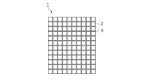
図1は実施形態のセラミックシンチレータアレイを示す平面図である。これらの図において、1はシンチレータアレイ、2はシンチレータセグメント、3は第一の反射層である。シンチレータアレイ1は複数のシンチレータセグメント2を有している。隣接するシンチレータセグメント2間には、第一の反射層3が介在している。第一の反射層3は隣接するシンチレータセグメント2に対してそれぞれ接着されている。複数のシンチレータセグメント2は、それらに接着された第一の反射層3で一体化されている。すなわち、シンチレータアレイ1は複数のシンチレータセグメント2を第一の反射層3で一体化した構造を有している。また、個々のシンチレータセグメント全体を覆うように第二の反射層が形成される(図1では省略されている)。
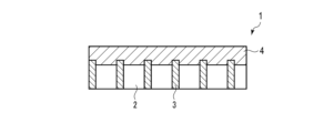
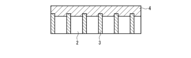
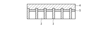
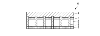
図2a~図2cは、本発明のシンチレータアレイの断面図の構成を3種類示したものである。図2aは各シンチレータセグメント間に介在する第一の反射層3とシンチレータアレイ全体を覆うように、X線入射側に配置された第二の反射層4が示されている。この場合、第二の反射層は、反射材を塗布し、さらに硬化したものである。図2bは図2aと類似のものであるが、さらにシンチレータセグメント間に介在する第一の反射層3の一部が第二の反射層4の内部に食い込む構成となっている。構成の詳細を説明する。第一の反射層3は、アレイ上面から第二の反射層4に向かう方向へ突き出た形状、すなわち、第二の反射層4側へ向けて凸部を有する。凸部のアレイ上面から第二の反射層4の上面までの距離(厚み)は、第二の反射層4の最大厚みより小さい。こうした構成とすることにより、シンチレータアレイからの第二の反射層の剥離を低減できる。図2cは予め反射粒子を含む樹脂でシート状に成型された第二の反射層4を、接着層5を介して張り合わせたものであるが、図2bと同様にシンチレータセグメント間に介在する第一の反射層3の一部が接着層5を通して第二の反射層4の内部に食い込む構成となっている。構成の詳細を説明する。第一の反射層3は、アレイ上面から第二の反射層4に向かう方向へ突き出た形状、すなわち、第二の反射層4側へ向けて凸部を有する。接着層5は、第二の反射層4の下面に形成され、第一の反射層3の凸部の上端付近と接している。凸部のアレイ上面から第二の反射層4の上面までの距離(厚み)は、第二の反射層4の最大厚みより小さい。図2bと図2cの構造により、第二の反射層の剥離をさらに低減でき、より好ましいものとなる。X線入射側と反対側には、シンチレータによりX線から可視光に変換された光を検出するフォトダイオードアレイが張り合わされ、本発明の放射線検出器となる。
DETAILED DESCRIPTION OF THE PREFERRED EMBODIMENTS Hereinafter, embodiments for carrying out the scintillator array, radiation detector, and radiation inspection apparatus of the present invention will be described.
(Ceramic scintillator array)
Fig. 1 is a plan view showing a ceramic scintillator array of an embodiment. In these figures, 1 is a scintillator array, 2 is a scintillator segment, and 3 is a first reflective layer. The
2a to 2c show three types of cross-sectional configurations of the scintillator array of the present invention. FIG. 2a shows a first reflecting
シンチレータアレイ1は、複数のシンチレータセグメント2を一列に並べた構造、もしくは図1に示すように複数のシンチレータセグメント2を縦方向および横方向に所定の個数ずつ2次元的に並べた構造のいずれを有していてもよい。複数のシンチレータセグメント2を2次元的に配列した場合、縦方向および横方向のシンチレータセグメント2間にそれぞれ第一の反射層3が設けられる。シンチレータセグメント2の個数は、X線検出器等の放射線検出器の構造や解像度等に応じて適宜に設定される。
The
シンチレータセグメント2は、希土類酸硫化物蛍光体の焼結体やガーネット構造酸化物の焼結体等からなるものである。シンチレータセグメント2は、1種類の焼結体または2種類以上の焼結体から形成される。希土類酸硫化物蛍光体セラミックとしては、付活剤としてプラセオジム(Pr)を含有する希土類酸硫化物蛍光体が例示される。蛍光体セラミックを構成する希土類酸硫化物としては、例えばイットリウム(Y)、ガドリニウム(Gd)、ランタン(La)、ルテチウム(Lu)等の希土類元素の酸硫化物が挙げられる。ガーネット構造酸化物の例として、ガドリニウム・ガリウム・アルミニウム・ガーネット(GGAG)、ルテチウム・アルミニウム・ガーネット(LuAG)、ルテチウム・ガリウム・アルミニウム・ガーネット(LuGAG)、ガドリニウム・アルミニウム・ガーネット(GdAG)、ガドリニウム・ガリウム・アルミニウム・ガーネット(GdGAG)などが挙げられる。ルテチウム・ガリウム・アルミニウム・ガーネット(LuGAG)が望ましい。
The
実施形態のセラミックシンチレータアレイ1において、シンチレータセグメント2は、
一般式:RE2O2S:Pr …(1)
(式中、REはY、Gd、La、およびLuからなる群より選ばれる少なくとも1つの元素を示す)
で表される組成を有する希土類酸硫化物蛍光体セラミック(シンチレータ材料)で構成されることが好ましい。
In the
General formula: RE2O2S : Pr ...(1)
(In the formula, RE represents at least one element selected from the group consisting of Y, Gd, La, and Lu).
It is preferable that the scintillator material is a rare earth oxysulfide phosphor ceramic (scintillator material) having a composition represented by the following formula:
上述した希土類元素のうち、特にGdはX線吸収係数が大きく、セラミックシンチレータアレイ1の光出力の向上に寄与する。従って、実施形態のシンチレータセグメント2には、Gd2O2S:Pr蛍光体を使用することがさらに好ましい。なお、Gdの一部は他の希土類元素で置換してもよい。この際、他の希土類元素によるGdの置換量は10モル%以下とすることが好ましい。
Among the rare earth elements described above, Gd has a particularly large X-ray absorption coefficient and contributes to improving the light output of the
すなわち、実施形態のセラミックシンチレータアレイ1においては、
一般式:(Gd1-X,REX)2O2S:Pr …(2)
(式中、REはY、La、およびLuからなる群より選ばれる少なくとも1つの元素を示し、Xは0≦X≦0.1を満足する数(原子比)である)で実質的に表される希土類酸硫化物蛍光体セラミックを、シンチレータセグメント2に使用することが望ましい。
That is, in the
General formula: (Gd 1-X , RE x ) 2 O 2 S:Pr...(2)
(wherein RE represents at least one element selected from the group consisting of Y, La, and Lu, and X is a number (atomic ratio) satisfying 0≦X≦0.1), it is desirable to use a rare earth oxysulfide phosphor ceramic for the
実施形態のセラミックシンチレータアレイ1においては、希土類酸硫化物蛍光体セラミックス(シンチレータ材料)の光出力を増大させる付活剤として、プラセオジム(Pr)を使用している。Prはさらに他の付活剤に比べてアフターグローの低減等を図ることができる。従って、付活剤としてPrを含有する希土類酸硫化物蛍光体セラミック(シンチレータ材料)は、放射線検出器の蛍光発生手段として有効である。
In the
希土類酸硫化物蛍光体セラミックにおけるPrの含有量は、蛍光体母体(例えばGd2O2SのようなRE2O2S)に対して0.001~10モル%の範囲とすることが好ましい。Prの含有量が10モル%を超えると、逆に光出力の低下を招くことになる。Prの含有量が0.001モル%未満では、主付活剤としての効果を十分に得ることができない。Prの含有量は0.01~1モル%の範囲であることがより好ましい。 The Pr content in the rare earth oxysulfide phosphor ceramic is preferably in the range of 0.001 to 10 mol % relative to the phosphor host (e.g., RE 2 O 2 S such as Gd 2 O 2 S). If the Pr content exceeds 10 mol %, it will result in a decrease in light output. If the Pr content is less than 0.001 mol %, it will not be possible to fully exert the effect as a main activator. It is more preferable that the Pr content be in the range of 0.01 to 1 mol %.
実施形態で使用する希土類酸硫化物蛍光体セラミックにおいては、主付活剤としてのPrに加えて、Ce、Zr、およびPからなる群より選ばれる少なくとも1つの元素を共付活剤として微量含有させてもよい。これらの元素は曝射劣化の抑制、アフターグローの抑制等に対して効果を示す。これら共付活剤の含有量は総量として、蛍光体母体に対して0.00001~0.1モル%の範囲とすることが好ましい。 The rare earth oxysulfide phosphor ceramic used in the embodiment may contain, in addition to Pr as the main activator, a small amount of at least one element selected from the group consisting of Ce, Zr, and P as a co-activator. These elements are effective in suppressing exposure degradation and afterglow. The total content of these co-activators is preferably in the range of 0.00001 to 0.1 mol% relative to the phosphor matrix.
さらに、実施形態のシンチレータセグメント2を形成するシンチレータ焼結体は、高純度の希土類酸硫化物系蛍光体セラミック(シンチレータ材料)からなることが好ましい。不純物はシンチレータの感度の低下要因となるため、できるだけ不純物量は低減することが好ましい。特に、燐酸根(PO4)は感度の低下原因となるため、その含有量は100ppm以下とすることが好ましい。フッ化物等を焼結助剤として使用して高密度化した場合、焼結助剤が不純物として残留するため、感度の低下をもたらすことになる。
Furthermore, the scintillator sintered body forming the
シンチレータセグメント2は、立方体形状または直方体形状の焼結体からなる。シンチレータセグメント2の体積は1mm3以下であることが好ましい。シンチレータセグメント2を小型化することによって、検出される画像を高精細化することができる。シンチレータセグメント2の縦(L)、横(S)、厚さ(T)の各サイズは必ずしも限定されるものではないが、それぞれ1mm以下であることが好ましい。シンチレータセグメント2の体積を1mm3以下と小型化した場合、第一の反射層3の幅(W)は100μm以下、さらには50μm以下と薄型化することも可能である。但し40μm未満とする場合は、製造プロセスが代わり煩雑となるため、第一の反射層3の幅(W)は40μm以上が好ましい。
実施形態のセラミックシンチレータアレイ1において、複数のシンチレータセグメント2を一体化する第一の反射層3は、透明樹脂と、透明樹脂中に分散された反射粒子とを含有する。透明樹脂としては、少なくともエポキシ樹脂、シリコーン樹脂、不飽和ポリエステル、ポリウレタン、アクリル樹脂,ポリエチレンテレフタレート、エポキシ変性シリコーン、グリシジルエーテルのいずれかひとつを含み、反射粒子として気泡もしくは顔料として酸化チタン、酸化アルミナ、硫酸バリウム、酸化亜鉛、酸化ジルコニウム,酸化シリコンのいずれか一つを含む、樹脂中に含まれる気泡も反射粒子としての役割を果たすことがある。セラミックシンチレータアレイ1を覆う反射層4は第一の反射層3と同様の透明樹脂及び反射粒子を用いることが出来る。なお、エポキシ樹脂、エポキシ変性シリコーン、グリシジルエーテルは、それぞれ、酸無水硬化剤を使用して硬化させた硬化物がC=O結合を含む。これら以外の樹脂、すなわち、シリコーン樹脂、不飽和ポリエステル、ポリウレタン、アクリル樹脂,ポリエチレンテレフタレートは、それぞれ、C=O結合を含むものである。
酸無水硬化剤の例として、水素化メチルナジック酸無水、エチレングリコールビス(アンヒドロトリメリテート)、メチルテトラヒドロ無水フタル酸、無水酸、無水トリメリット酸、ドデセニル無水コハク酸、ベンゾフェノンテトラカルボン酸無水物、メチルテトラヒドロ無水フタル酸、メチルヘキサヒドロフタル酸、トリアルキルテトラヒドロ無水フタル酸マレイン酸付加物、4-メチルヘキサヒドロ無水フタル酸、3-メチルヘキサヒドロ無水フタル酸、トリアルキルテトラヒドロ無水フタル酸、メチルテトラヒドロ無水フタル酸、クロレンド酸無水物、ヘキサヒドロ無水フタル酸、テトラヒドロ無水フタル酸、無水コハク酸、3or4-メチル1,2,3,6-テトラヒドロ無水フタル酸、3or4-メチル-ヘキサヒドロ無水フタル酸、メチル-3,6-エンドメチレン-1,2,3,6-テトラヒドロ無水フタル酸、無水マレイン酸、無水フタル酸、無水ピロリット酸、メチルシクロヘキセンテトラカルボン酸二無水物、グリセリンビス(アンヒドロトリメリテート)モノアセテート、脂肪族二塩基酸ポリ無水物等が挙げられる。使用する酸無水硬化剤の種類は1種または2種以上にすることができる。
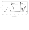
X線によって一般的に樹脂は着色(黄変)する傾向があり、その着色によってシンチレータ内で発生した光は吸収されてしまい,光出力が低下してしまう。しかし,樹脂の骨格によって黄変の度合いが異なる。フーリエ変換赤外分光法(FT-IR)により、1490cm-1~1750cm-1の帯域(波数域1)はエステル基、カルボキシル基、ケト基(ケトン基)などのC=Oに起因する吸収が現れる。また、2500cm-1~2990cm-1の帯域(波数域2)にはC―H結合による吸収が見受けられる。多くの実験結果を通し、反射材のX線による変色が小さいものは、波数域1に於ける吸収ピーク面積の、波数域2に於ける吸収ピーク面積に対する比率、すなわちピーク面積比が、一定の範囲にあるものが好ましいことが分かった。
図3は本発明のシンチレータアレイの反射層について、フーリエ変換赤外分光法(FT-IR)による赤外吸収スペクトルを示したものである。1490cm-1~1750cm-1の帯域(波数域1)、2500cm-1~2990cm-1の帯域(波数域2)にそれぞれ吸収ピークが認められ、これらは含まれる顔料ではなく樹脂に起因するものである。吸収ピーク面積とは、図3に点線で示されたベースラインから上の面積を意味する。本発明では、それぞれの吸収ピーク面積の波数域1の波数域2に対する比率が0.01~4の範囲の値を有するものである。上記比率は3.6以下が好ましい。より好ましくは0.1~2.5の範囲である。図3に示されたような赤外吸収スペクトルは、シンチレータアレイから、反射層を剥離させる、また一部を削り取るなどして容易に測定することが可能である。
The
In the
Examples of the acid anhydride hardener include hydrogenated methylnadic anhydride, ethylene glycol bis(anhydrotrimellitate), methyltetrahydrophthalic anhydride, acid anhydride, trimellitic anhydride, dodecenyl succinic anhydride, benzophenone tetracarboxylic anhydride, methyltetrahydrophthalic anhydride, methylhexahydrophthalic anhydride, trialkyltetrahydrophthalic anhydride maleic anhydride, 4-methylhexahydrophthalic anhydride, 3-methylhexahydrophthalic anhydride, trialkyltetrahydrophthalic anhydride, methyltetrahydro Examples of the acid anhydride include phthalic anhydride, chlorendic anhydride, hexahydrophthalic anhydride, tetrahydrophthalic anhydride, succinic anhydride, 3 or 4-methyl-1,2,3,6-tetrahydrophthalic anhydride, 3 or 4-methyl-hexahydrophthalic anhydride, methyl-3,6-endomethylene-1,2,3,6-tetrahydrophthalic anhydride, maleic anhydride, phthalic anhydride, pyrrolic anhydride, methylcyclohexenetetracarboxylic dianhydride, glycerin bis(anhydrotrimellitate) monoacetate, aliphatic dibasic acid polyanhydrides, etc. The type of the acid anhydride curing agent used may be one or more types.
Generally, resins tend to become colored (yellowing) by X-rays, and this coloring causes the light generated in the scintillator to be absorbed, resulting in a decrease in light output. However, the degree of yellowing varies depending on the skeleton of the resin. Fourier transform infrared spectroscopy (FT-IR) shows that in the band of 1490 cm -1 to 1750 cm -1 (wave number range 1), absorption due to C=O such as ester groups, carboxyl groups, and keto groups (ketone groups) appears. In addition, absorption due to C-H bonds is seen in the band of 2500 cm -1 to 2990 cm -1 (wave number range 2). Through many experimental results, it has been found that reflective materials that do not discolor due to X-rays are preferable when the ratio of the absorption peak area in
FIG. 3 shows an infrared absorption spectrum of the reflective layer of the scintillator array of the present invention, measured by Fourier transform infrared spectroscopy (FT-IR). Absorption peaks are observed in the band of 1490 cm -1 to 1750 cm -1 (wave number range 1) and the band of 2500 cm -1 to 2990 cm -1 (wave number range 2), and these are due to the resin, not the pigment contained therein. The absorption peak area means the area above the baseline shown by the dotted line in FIG. 3. In the present invention, the ratio of the absorption peak area of
第一の反射層3および第二の反射層4を形成する透明樹脂と反射粒子の割合は、透明樹脂の質量比が15~60%、反射粒子の質量比が40~85%(透明樹脂の質量比+反射粒子の質量比=100%とする)であることが好ましい。反射粒子の質量比が40%未満では、反射層の反射効率が低下し、波長512nmの光に対する反射層の反射効率が90%より低くなりやすい。反射粒子の質量比が85%を超えると、反射層の反射効率は変わらないが、透明樹脂の質量比が相対的に減るために、反射層の安定した固体化が難しくなる。
実施形態のセラミックシンチレータアレイ1に、予め作製された第二の反射層を張り合わせた構成とする場合には、接着層としては少なくともエポキシ樹脂、シリコーン樹脂、アクリル樹脂、ウレタン樹脂,ポリエステル樹脂を含み、光、熱、湿気のいずれかにより硬化する樹脂を用いる。接着層は透明樹脂でもよいが、接着層に気泡もしくは顔料として酸化チタン、酸化アルミナ、硫酸バリウム、酸化亜鉛、酸化ジルコニウム,酸化シリコンのいずれか一つを含んでいても良い。
本発明のシンチレータアレイは次のように製造される。好ましい構成である図2cの場合を例にとって説明する。第1工程では、白色反射材を含むエポキシ等の樹脂で白色シートを形成し、所定の大きさのものを用意する。白色シートには、反射粒子と透明樹脂との混合物やラッカー系塗料等が用いられる。反射粒子と透明樹脂との混合物は、シンチレータセグメント間の反射層と同様な構成を有していることが好ましい。白色シートは白色PETフィルムなど市販のものを用いても良い。白色シートはシンチレータアレイの第二の反射層になるもので、その厚さは50~500μmの範囲である。第二の反射層の厚さが50μm未満であると、反射効率の向上効果を十分に得ることができない。第二の反射層の厚さが250μmを超えると、透過するX線量が低下して検出感度が低下する。また別に希土類酸硫化物系蛍光体セラミック等のシンチレータ材料を所定の大きさの薄板(厚さ0.5~2mm)として切り出し、前記白色シートに貼り合わせる。薄板は一枚のセラミック板あるいは複数のセラミック板を端面同士で突き合わせて,白色シートにエポキシ樹脂や熱可塑性接着剤等で接着する。突き合わせた際の境界部の隙間の幅は工程2での溝加工の幅より小さいことが好ましい。
第2工程ではダイシングによる溝加工を施す。溝の幅は40~200μmの範囲である。溝はセラミックシンチレータ材の方から形成し、セラミックシンチレータ材料、接着層、さらに白色シート内に達するものである。溝加工する位置は,前記複数のセラミック板を突き合わせた境界面が溝部になるように調整する.白色シート内の溝を埋めるように、セグメント間の反射層(第一反射層)の一部が設けられ、そのアンカー効果により、天板反射層(第二の反射層)の剥離を防止することができる。第3工程は第2工程で形成された溝に反射層を設ける工程である。
まず、反射粒子と透明樹脂を構成する未硬化状態の樹脂組成物(透明樹脂の未硬化物)とを用意し、その混合物を、シンチレータセグメント間の溝に充填する。未硬化状態の樹脂組成物は、0.2~1Pa・s(200~1000cps)の粘度を有することが好ましい。樹脂組成物の粘度が0.2Pa・s未満では流動性が高く、シンチレータセグメント間への充填作業性が低下する。樹脂組成物の粘度が1Pa・sを超えると、流動性が低下し、そのため塗布性または充填性が低下する。また、透明樹脂の全光線透過率は85%以上であることが好ましい。透明樹脂の全光線透過率が85%未満であると、反射層の反射効率が低下しやすくなる。
The ratio of the transparent resin and the reflective particles forming the first
In the case of a configuration in which a prefabricated second reflective layer is bonded to the
The scintillator array of the present invention is manufactured as follows. The preferred structure shown in FIG. 2c will be taken as an example. In the first step, a white sheet is formed of a resin such as epoxy containing a white reflective material, and a sheet of a predetermined size is prepared. A mixture of reflective particles and transparent resin, a lacquer-based paint, or the like is used for the white sheet. The mixture of reflective particles and transparent resin preferably has a structure similar to that of the reflective layer between the scintillator segments. The white sheet may be a commercially available product such as a white PET film. The white sheet is the second reflective layer of the scintillator array, and has a thickness in the range of 50 to 500 μm. If the thickness of the second reflective layer is less than 50 μm, the effect of improving the reflection efficiency cannot be sufficiently obtained. If the thickness of the second reflective layer exceeds 250 μm, the amount of X-rays transmitted is reduced, and the detection sensitivity is reduced. Separately, a scintillator material such as a rare earth oxysulfide phosphor ceramic is cut into a thin plate of a predetermined size (thickness 0.5 to 2 mm) and pasted onto the white sheet. The thin plate is made by butting the end faces of one ceramic plate or multiple ceramic plates together and bonding them to the white sheet with epoxy resin, thermoplastic adhesive, etc. It is preferable that the width of the gap at the boundary when they are butted together is smaller than the width of the groove processed in
In the second step, grooves are made by dicing. The width of the grooves is in the range of 40 to 200 μm. The grooves are made from the ceramic scintillator material, and reach the ceramic scintillator material, the adhesive layer, and even into the white sheet. The position of the grooves is adjusted so that the boundary surface where the multiple ceramic plates are butted together becomes the groove portion. Part of the reflective layer (first reflective layer) between the segments is provided so as to fill the grooves in the white sheet, and the anchor effect of this prevents the top plate reflective layer (second reflective layer) from peeling off. The third step is to provide a reflective layer in the grooves made in the second step.
First, the reflective particles and the uncured resin composition (uncured transparent resin) constituting the transparent resin are prepared, and the mixture is filled into the grooves between the scintillator segments. The uncured resin composition preferably has a viscosity of 0.2 to 1 Pa·s (200 to 1000 cps). If the viscosity of the resin composition is less than 0.2 Pa·s, the fluidity is high and the workability of filling between the scintillator segments is reduced. If the viscosity of the resin composition exceeds 1 Pa·s, the fluidity is reduced, and therefore the coating property or filling property is reduced. In addition, the total light transmittance of the transparent resin is preferably 85% or more. If the total light transmittance of the transparent resin is less than 85%, the reflection efficiency of the reflective layer is likely to decrease.
複数のシンチレータセグメント間に反射粒子と未硬化状態の樹脂組成物との混合物を充填した後、混合物中の樹脂組成物を硬化させて反射層を形成する。混合物の硬化処理は、未硬化状態の樹脂組成物や硬化剤の種類等に応じて適宜に設定される。例えば、熱硬化性樹脂組成物の場合には、熱処理することにより硬化反応を進行させる。2液型のエポキシ樹脂のような樹脂組成物として、室温下で放置することにより硬化反応を進行させる場合もある。次に工程4では、外周の不要分を取り除く外周加工、さらに研磨をすることにより本発明のシンチレータアレイが完成する。
(放射線検出器)
実施形態の放射線検出器は、上述した実施形態のセラミックシンチレータアレイ1を、入射した放射線に応じて光を放射する蛍光発生手段として具備し、さらに蛍光発生手段からの光を受け、光の出力を電気的出力に変換する光電変換手段を具備する。図4は実施形態の放射線検出器の一例であるX線検出器を示している。図4に示すX線検出器6は、蛍光発生手段としてセラミックシンチレータアレイ1と、光電変換手段としてフォトダイオードのような光電変換素子7とを具備している。セラミックシンチレータアレイ1の構成は、図2cを参照して説明したものと同様である。そのため、図2cと同符号を付して説明を省略する。
A mixture of reflective particles and an uncured resin composition is filled between the scintillator segments, and then the resin composition in the mixture is cured to form a reflective layer. The curing treatment of the mixture is appropriately set according to the type of uncured resin composition and curing agent. For example, in the case of a thermosetting resin composition, the curing reaction is advanced by heat treatment. In some cases, the curing reaction of a resin composition such as a two-liquid epoxy resin is advanced by leaving it at room temperature. Next, in
(Radiation detector)
The radiation detector of the embodiment includes the
セラミックシンチレータアレイ1はX線入射面を有し、X線入射面とは反対側の面には光電変換素子7が一体的に設置されている。光電変換素子7としては、例えばフォトダイオードが使用される。光電変換素子7は、セラミックシンチレータアレイ1を構成する複数のシンチレータセグメント2のそれぞれに対応するように配置されている。これらによって、放射線検出器が構成されている。
(放射線検査装置)
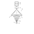
実施形態の放射線検査装置は、被検査体に向けて放射線を照射する放射線源と、被検査体を透過した放射線を検出する放射線検出器とを具備する。放射線検出器には、上述した実施形態の放射線検出器が用いられる。図5は実施形態の放射線検査装置の一例であるX線CT装置10を示している。図5において、10はX線CT装置、11は被検体、12はX線管、13はコンピュータ、14はディスプレイ、15は被検体画像である。X線CT装置10は、実施形態のX線検出器6を備えている。X線検出器6は、例えば被検体11の撮像部位が配置される円筒の内壁面に貼り付けられている。X線検出器6が貼り付けられた円筒の円弧の略中心には、X線を出射するX線管12が設置されている。X線検出器6とX線管12との間には被検体11が配置される。X線検出器6のX線入射面側には、図示しないコリメータが設けられている。
The
(Radiation Inspection Equipment)
The radiation inspection apparatus of the embodiment includes a radiation source that irradiates radiation toward an object to be inspected, and a radiation detector that detects radiation that has passed through the object to be inspected. The radiation detector of the above-described embodiment is used as the radiation detector. FIG. 5 shows an
X線検出器6およびX線管12は、被検体11を中心にしてX線による撮影を行いながら回転するように構成されている。被検体11の画像情報が異なる角度から立体的に集められる。X線撮影により得られた信号(光電変換素子により変換された電気信号)はコンピュータ13で処理され、ディスプレイ14上に被検体画像15として表示される。被検体画像15は、例えば被検体11の断層像である。図1に示すように、シンチレータセグメント2を2次元的に配置したシンチレータアレイ1を用いることによって、マルチ断層像タイプのX線CT装置10を構成することも可能である。この場合、被検体11の断層像が複数同時に撮影され、例えば撮影結果を立体的に描写することもできる。
The
図5に示すX線CT装置10は、実施形態のセラミックシンチレータアレイ1を有するX線検出器6を具備している。前述したように、実施形態のセラミックシンチレータアレイ1は第一の反射層3及び第二の反射層4の構成等に基づいて、シンチレータセグメント2から放射される可視光の反射効率が高いため、優れた光出力を有している。このようなシンチレータアレイ1を有するX線検出器6を使用することによって、X線CT装置10による撮影時間を短くすることができる。その結果、被検体11の被爆時間を短くすることができ、低被爆化を実現することが可能になる。実施形態の放射線検査装置(X線CT装置10)は、人体の医療診断用のX線検査に限らず、動物のX線検査や工業用途のX線検査等に対しても適用可能である。さらに、X線非破壊検査装置による検査精度の向上等にも寄与する。
The
次に、本発明の具体的な実施例およびその評価結果について述べる。
(実施例1~6、比較例1~2)
各樹脂材料に酸化チタン(石原産業製CR-90)を60wt%混練し,硬化物を作製した。FT-IR(日本分光製FT/IR-6600)にて作製した硬化物の赤外吸収スペクトルを取得し,1490~1750cm-1のピークと2500~2990cm-1のピークの面積を算出した。2500~2990cm-1のピークに対する1490~1750cm-1のピークの面積比率を求めた。また,作製した硬化物にX線を4.2kGy照射し,照射部と未照射部の反射率(波長510nmと670nmの平均)を測定し,その差を反射率の低下率として算出した。その結果を表1に示す。反射率の低下率(%)の詳細を以下に記載する。分光反射率測定計にて、X線照射部と未照射部の反射率をそれぞれ波長510nmと670nmにて測定した。それぞれの箇所で測定した2つの波長の反射率の平均値を求め、X線照射部の反射率から未照射部の反射率を引いた差(低下率%)を算出した。フーリエ変換赤外分光法(FT-IR)の面積比率が小さいほど、X線照射での反射率の低下率は小さくなる傾向にある。
Next, specific examples of the present invention and the results of evaluation thereof will be described.
(Examples 1 to 6, Comparative Examples 1 to 2)
Each resin material was mixed with 60 wt% titanium oxide (CR-90, manufactured by Ishihara Sangyo Kaisha, Ltd.) to prepare a cured product. The infrared absorption spectrum of the prepared cured product was obtained using an FT-IR (FT/IR-6600, manufactured by JASCO Corporation), and the areas of the peaks at 1490-1750 cm -1 and 2500-2990 cm -1 were calculated. The area ratio of the peak at 1490-1750 cm -1 to the peak at 2500-2990 cm -1 was calculated. In addition, the prepared cured product was irradiated with X-rays at 4.2 kGy, and the reflectance (average of wavelengths of 510 nm and 670 nm) of the irradiated and unirradiated areas was measured, and the difference was calculated as the decrease in reflectance. The results are shown in Table 1. The details of the decrease in reflectance (%) are described below. The reflectance of the X-ray irradiated and unirradiated areas was measured at wavelengths of 510 nm and 670 nm using a spectroscopic reflectance meter. The reflectance of the non-irradiated area was calculated by subtracting the reflectance of the irradiated area from the reflectance of the irradiated area (reduction rate %). The smaller the area ratio of Fourier transform infrared spectroscopy (FT-IR), the smaller the reduction rate of reflectance due to X-ray irradiation tends to be.
実施例1~6の硬化物は、それぞれ、C=O結合を含む。これに対し、比較例1,2の硬化物は、C=O結合を持たない。 The cured products of Examples 1 to 6 each contain a C=O bond. In contrast, the cured products of Comparative Examples 1 and 2 do not have a C=O bond.
(実施例8、9、比較例3、4)
実施例1,4と比較例1,2の樹脂を用いて、シンチレータアレイを形成した。Gd2O2S:Pr(Pr濃度=0.05モル%)の組成を有する蛍光体粉末をラバープレスにより仮成形し、この仮成形体をTa製のカプセル中に脱気密封した後、これをHIP処理装置にセットした。HIP処理装置にアルゴンガスを加圧媒体として封入し、圧力147MPa、温度1425℃の条件で3時間処理した。このようにして、直径約80mm×高さ約120mmの円柱状の焼結体を作製した。この焼結体からGOSセラミック板を切り出した。
長さ70mm、幅22mm、厚み2mmのGOSセラミック板を2枚,長辺同士を突き合わせ,その表面に一回り面積が大きい白色PETフィルム(三菱ケミカル製,厚み100μm)をエポキシ接着材で貼り合わせた。張り合わせる際にはGOSセラミック板、エポキシ接着材、白色PETシートを重ねて、荷重16kg印加し、100℃で加熱して接着した。常温まで冷却後に荷重を除き,長さ70mm,幅44mmの積層体を完成させた。
この積層体のGOSセラミック板表面にダイシングによる溝加工を施した。このとき、溝の深さは2.1mmで形成した。溝は白色PETシートまで形成されている。また,溝の位置は2つのセラミック板の境界が溝になるように溝加工位置を調整した.溝に酸化チタンを混合した実施例1,4及び比較例1,2の樹脂材料を流し込み、熱硬化,研磨した。その後、外周部をカットし、長さ66mm,幅40mm,厚さ1.99mmの図2cに相当するシンチレータアレイを作製した。
本発明のシンチレータアレイでは、比較例に対して,実施例に示したとおり,フーリエ変換赤外分光法(FT-IR)において、波数域1(1490cm-1~1750cm-1)の吸収ピーク面積の、波数域2(2500cm-1~2990cm-1)の吸収ピーク面積に対する比率(ピーク面積比)が小さい樹脂を反射層にもちいることで,X線照射による光出力の低下を小さくすることが認められた.本発明の対策がその方向として有効なものであることは疑いない。
(Examples 8 and 9, Comparative Examples 3 and 4)
A scintillator array was formed using the resins of Examples 1 and 4 and Comparative Examples 1 and 2. A phosphor powder having a composition of Gd2O2S :Pr (Pr concentration = 0.05 mol%) was provisionally molded by a rubber press, and the provisionally molded body was degassed and sealed in a capsule made of Ta, and then set in a HIP processing device. Argon gas was sealed in the HIP processing device as a pressure medium, and the HIP processing device was treated for 3 hours under conditions of a pressure of 147 MPa and a temperature of 1425°C. In this way, a cylindrical sintered body with a diameter of about 80 mm and a height of about 120 mm was produced. A GOS ceramic plate was cut out from the sintered body.
Two GOS ceramic plates, 70 mm long, 22 mm wide, and 2 mm thick, were butted together with their long sides, and a white PET film (100 μm thick, manufactured by Mitsubishi Chemical) with a larger area was attached to the surface with an epoxy adhesive. When attaching, the GOS ceramic plate, epoxy adhesive, and white PET sheet were stacked, and a load of 16 kg was applied and heated to 100° C. to bond them. After cooling to room temperature, the load was removed, completing a laminate with a length of 70 mm and a width of 44 mm.
The surface of the GOS ceramic plate of this laminate was grooved by dicing. The groove was formed to a depth of 2.1 mm. The groove was formed up to the white PET sheet. The groove position was adjusted so that the boundary between the two ceramic plates was the groove. The resin material of Examples 1 and 4 and Comparative Examples 1 and 2 mixed with titanium oxide was poured into the groove, heat-cured, and polished. The outer periphery was then cut to produce a scintillator array corresponding to Figure 2c, with a length of 66 mm, a width of 40 mm, and a thickness of 1.99 mm.
As shown in the Examples, in the scintillator array of the present invention, in comparison with the Comparative Examples, it was found that the decrease in light output due to X-ray irradiation was reduced by using a resin for the reflective layer that has a smaller ratio (peak area ratio) of the absorption peak area in wavenumber range 1 (1490 cm -1 to 1750 cm -1 ) to the absorption peak area in wavenumber range 2 (2500 cm -1 to 2990 cm -1 ) in Fourier transform infrared spectroscopy (FT-IR). There is no doubt that the measures of the present invention are effective in that direction.
以下、出願当初の発明を付記する。
[1]
希土類酸硫化物蛍光体の焼結体で構成されるセラミックシンチレータアレイであって、複数のシンチレータセグメントと、前記複数のシンチレータセグメントを一体化するように、シンチレータセグメント間に設けられた反射層部を有し、前記反射層は、C=C結合を含まない樹脂を含み、赤外分光により、前記反射層を構成する反射材が1490cm-1~1750cm-1の波数域1と,2500cm-1~2990cm-1の波数域2に吸収ピークをもち,波数域2に対する波数域1のピークの面積比が0.01~4であることを特徴とするセラミックシンチレータアレイ。
[2]
前記[1]記載のセラミックシンチレータアレイにおいて、セグメント間反射層及び天板反射層は少なくともエポキシ樹脂、シリコーン樹脂、不飽和ポリエステル、ポリウレタン、アクリル樹脂,ポリエチレンテレフタレートのいずれか一つを含み、気泡もしくは顔料として酸化チタン、酸化アルミナ、硫酸バリウム、酸化亜鉛、酸化ジルコニウム,酸化シリコンのいずれか一つを含むことを特徴とするセラミックシンチレータアレイ。
[3]
[1]~[2]記載のセラミックシンチレータアレイにおいて、天板反射層は接着層を介して付設されていることを特徴とするセラミックシンチレータアレイ。
[4]
[1]~[3]記載のセラミックシンチレータアレイにおいて、希土類酸硫化物蛍光体は、
一般式:RE2O2S:Pr
(ここで、REはY、Gd、La、およびLuからなる群より選ばれる少なくとも1つである)で表され、RE2O2Sに対するPrの含有量が0.001モル%以上10モル%以下である組成を有することを特徴とするセラミックシンチレータアレイ。
[5]
[1]~[4]記載のセラミックシンチレータアレイを具備する放射線検出器。
[6]
[5]記載の放射線検出器を具備する放射線検査装置。
<1>
少なくとも2つのシンチレータセグメントと、前記2つのシンチレータセグメント間に設けられた第一の反射層と、を備え、前記第一の反射層は、C=O結合を有する樹脂を含む、シンチレータアレイ。
<2>
前記第一の反射層は、エポキシ樹脂、シリコーン樹脂、不飽和ポリエステル、ポリウレタン、アクリル樹脂,ポリエチレンテレフタレート、エポキシ変性シリコーン、グリシジルエーテルのうち、少なくともいずれか一つを含む、<1>に記載のシンチレータアレイ。
<3>
前記樹脂は、エステル基、カルボキシル基、ケト基のうち、少なくともいずれか一つを含む、<1>に記載のシンチレータアレイ。
<4>
前記第一の反射層は、酸化チタン、酸化アルミナ、硫酸バリウム、酸化亜鉛、酸化ジルコニウム,酸化シリコン、気泡のうち、少なくともいずれか一つを含む、<1>~<3>のいずれか1項に記載のシンチレータアレイ。
<5>
前記2つのシンチレータセグメント上及び前記第一の反射層上に設けられ、前記第一の反射層と同じ樹脂を含む第二の反射層と、を更に備える、<1>~<4>のいずれか1項に記載のシンチレータアレイ。
<6>
前記シンチレータセグメントは、希土類酸硫化物蛍光体、もしくはガーネット構造酸化物蛍光体を含む、<1>~<5>のいずれか1項に記載のシンチレータアレイ。
<7>
少なくとも2つのシンチレータセグメントと、前記2つのシンチレータセグメント間に設けられた第一の反射層と、を備え、前記第一の反射層は、赤外分光により1490cm-1~1750cm-1の波数域1と2500cm-1~2990cm-1の波数域2に吸収ピークを有し、波数域2に対する波数域1のピークの面積比が0.01~4である、シンチレータアレイ。
<8>
前記波数域2に対する前記波数域1のピークの面積比が3.6以下である、<7>に記載のシンチレータアレイ。
<9>
前記2つのシンチレータセグメント上及び前記第一の反射層上に設けられ、前記第一の反射層と同じ樹脂を含む第二の反射層と、を更に備える、<7>または<8>に記載のシンチレータアレイ。
<10>
前記シンチレータセグメントは、希土類酸硫化物蛍光体、もしくはガーネット構造酸化物蛍光体を含む、<7>~<9>のいずれか1項に記載のシンチレータアレイ。
<11>
<1>~<10>のいずれか1項に記載のシンチレータアレイを具備する放射線検出器。
<12>
<11>に記載の放射線検出器を具備する放射線検査装置。
(1)
焼結体からなる少なくとも2つのシンチレータセグメントと、前記2つのシンチレータセグメント間に設けられた第一の反射層と、を備え、前記第一の反射層は、C=O結合を有する樹脂と、前記樹脂中に分散された反射粒子とを含む、シンチレータアレイ。
(2)
前記第一の反射層は、エポキシ樹脂、シリコーン樹脂、不飽和ポリエステル、ポリウレタン、アクリル樹脂,ポリエチレンテレフタレート、エポキシ変性シリコーン、グリシジルエーテルのうち、少なくともいずれか一つを含む、(1)に記載のシンチレータアレイ。
(3)
前記樹脂は、エステル基、カルボキシル基、ケト基のうち、少なくともいずれか一つを含む、(1)に記載のシンチレータアレイ。
(4)
前記第一の反射層は、前記2つのシンチレータセグメントの間を埋め尽くすように設けられる、(1)~(3)のいずれか1項に記載のシンチレータアレイ。
(5)
前記第一の反射層は、前記2つのシンチレータセグメントの間に充填して設けられる、(1)~(3)のいずれか1項に記載のシンチレータアレイ。
(6)
前記第一の反射層の前記反射粒子は、酸化チタン、酸化アルミナ、硫酸バリウム、酸化亜鉛、酸化ジルコニウム,酸化シリコン、気泡のうち、少なくともいずれか一つを含む、(1)~(5)のいずれか1項に記載のシンチレータアレイ。
(7)
前記2つのシンチレータセグメント上及び前記第一の反射層上に設けられ、前記第一の反射層と同じ樹脂を含む第二の反射層と、を更に備える、(1)~(6)のいずれか1項に記載のシンチレータアレイ。
(8)
前記シンチレータセグメントの前記焼結体は、希土類酸硫化物蛍光体の焼結体、もしくはガーネット構造酸化物蛍光体の焼結体を含む、(1)~(7)のいずれか1項に記載のシンチレータアレイ。
(9)
少なくとも2つのシンチレータセグメントと、前記2つのシンチレータセグメント間に設けられた第一の反射層と、を備え、前記第一の反射層は、赤外分光により1490cm-1~1750cm-1の波数域1と2500cm-1~2990cm-1の波数域2に吸収ピークを有し、波数域2に対する波数域1のピークの面積比が0.01~4である、シンチレータアレイ。
(10)
前記波数域2に対する前記波数域1のピークの面積比が3.6以下である、(9)に記載のシンチレータアレイ。
(11)
前記2つのシンチレータセグメント上及び前記第一の反射層上に設けられ、前記第一の反射層と同じ樹脂を含む第二の反射層と、を更に備える、(9)または(10)に記載のシンチレータアレイ。
(12)
前記シンチレータセグメントは、希土類酸硫化物蛍光体、もしくはガーネット構造酸化物蛍光体を含む、(9)~(11)のいずれか1項に記載のシンチレータアレイ。
(13)
(1)~(12)のいずれか1項に記載のシンチレータアレイを具備する放射線検出器。
(14)
(13)に記載の放射線検出器を具備する放射線検査装置。
The invention as originally filed is described below.
[1]
A ceramic scintillator array composed of a sintered body of a rare earth oxysulfide phosphor, comprising a plurality of scintillator segments and a reflective layer portion provided between the scintillator segments so as to integrate the plurality of scintillator segments, the reflective layer containing a resin that does not contain a C=C bond, and characterized in that, by infrared spectroscopy, the reflective material constituting the reflective layer has absorption peaks in a
[2]
In the ceramic scintillator array described in [1] above, the inter-segment reflective layer and the top plate reflective layer contain at least one of epoxy resin, silicone resin, unsaturated polyester, polyurethane, acrylic resin, and polyethylene terephthalate, and contain as bubbles or pigments one of titanium oxide, alumina oxide, barium sulfate, zinc oxide, zirconium oxide, and silicon oxide.
[3]
3. The ceramic scintillator array according to
[4]
In the ceramic scintillator array according to any one of [1] to [3], the rare earth oxysulfide phosphor is
General formula: RE 2 O 2 S: Pr
(wherein RE is at least one selected from the group consisting of Y, Gd, La, and Lu), and the content of Pr relative to RE2O2S is 0.001 mol % or more and 10 mol % or less.
[5]
A radiation detector comprising the ceramic scintillator array according to any one of [1] to [4].
[6]
[5] A radiation inspection device comprising the radiation detector according to the present invention.
<1>
A scintillator array comprising at least two scintillator segments and a first reflective layer provided between the two scintillator segments, the first reflective layer including a resin having a C═O bond.
<2>
The scintillator array according to <1>, wherein the first reflective layer contains at least one of an epoxy resin, a silicone resin, an unsaturated polyester, a polyurethane, an acrylic resin, polyethylene terephthalate, an epoxy-modified silicone, and a glycidyl ether.
<3>
The scintillator array according to <1>, wherein the resin contains at least one of an ester group, a carboxyl group, and a keto group.
<4>
The scintillator array according to any one of <1> to <3>, wherein the first reflective layer contains at least one of titanium oxide, alumina oxide, barium sulfate, zinc oxide, zirconium oxide, silicon oxide, and air bubbles.
<5>
<4> The scintillator array according to any one of <1> to <4>, further comprising: a second reflective layer provided on the two scintillator segments and the first reflective layer, the second reflective layer containing the same resin as the first reflective layer.
<6>
The scintillator array according to any one of <1> to <5>, wherein the scintillator segments contain a rare earth oxysulfide phosphor or a garnet-structure oxide phosphor.
<7>
A scintillator array comprising at least two scintillator segments and a first reflective layer provided between the two scintillator segments, wherein the first reflective layer has absorption peaks in a
<8>
The scintillator array according to <7>, wherein the peak area ratio of the
<9>
The scintillator array according to <7> or <8>, further comprising: a second reflective layer provided on the two scintillator segments and the first reflective layer, the second reflective layer containing the same resin as the first reflective layer.
<10>
The scintillator array according to any one of <7> to <9>, wherein the scintillator segments contain a rare earth oxysulfide phosphor or a garnet-structure oxide phosphor.
<11>
A radiation detector comprising the scintillator array according to any one of <1> to <10>.
<12>
A radiation inspection device comprising the radiation detector according to <11>.
(1)
A scintillator array comprising at least two scintillator segments made of a sintered body and a first reflective layer provided between the two scintillator segments, the first reflective layer including a resin having a C=O bond and reflective particles dispersed in the resin.
(2)
2. The scintillator array according to
(3)
The scintillator array according to (1), wherein the resin contains at least one of an ester group, a carboxyl group, and a keto group.
(4)
The scintillator array according to any one of (1) to (3), wherein the first reflective layer is provided so as to completely fill the space between the two scintillator segments.
(5)
The scintillator array according to any one of (1) to (3), wherein the first reflective layer is provided by filling a space between the two scintillator segments.
(6)
The scintillator array according to any one of (1) to (5), wherein the reflective particles of the first reflective layer include at least one of titanium oxide, alumina oxide, barium sulfate, zinc oxide, zirconium oxide, silicon oxide, and air bubbles.
(7)
The scintillator array according to any one of (1) to (6), further comprising a second reflective layer provided on the two scintillator segments and the first reflective layer, the second reflective layer containing the same resin as the first reflective layer.
(8)
The scintillator array according to any one of (1) to (7), wherein the sintered body of the scintillator segment includes a sintered body of a rare earth oxysulfide phosphor or a sintered body of a garnet-structure oxide phosphor.
(9)
A scintillator array comprising at least two scintillator segments and a first reflective layer provided between the two scintillator segments, wherein the first reflective layer has absorption peaks in a
(10)
The scintillator array according to (9), wherein the area ratio of the peak in the
(11)
The scintillator array of
(12)
The scintillator array according to any one of (9) to (11), wherein the scintillator segments contain a rare earth oxysulfide phosphor or a garnet-structure oxide phosphor.
(13)
A radiation detector comprising the scintillator array according to any one of (1) to (12).
(14)
(13) A radiation inspection device comprising the radiation detector according to (13).
本発明のシンチレータアレイによれば、X線照射による光出力の低下を小さくすることができるため、産業上有用なものと言える。 The scintillator array of the present invention can reduce the decrease in light output due to X-ray irradiation, making it industrially useful.
1 シンチレータアレイ
2 シンチレータセグメント
3 シンチレータセグメント間の反射層
4 X線入射面側のシンチレータアレイに付設される反射層(第二の反射層)
5 接着層
6 X線検出器
7 光電変換素子
1
5
Claims (10)
C=O結合を有する樹脂と反射粒子とを含み、赤外分光法において1490cm-1~1750cm-1の波数域1と2500cm-1~2990cm-1の波数域2に吸収ピークを有し、波数域2の吸収ピーク面積に対する波数域1の吸収ピークの面積の比が0.01以上4以下である第一の反射層と
を備える、シンチレータアレイ。 A plurality of scintillator segments;
a first reflective layer that includes a resin having a C═O bond and reflective particles, and that has absorption peaks in a wavenumber region 1 of 1490 cm −1 to 1750 cm −1 and a wavenumber region 2 of 2500 cm −1 to 2990 cm −1 in infrared spectroscopy, and the ratio of the area of the absorption peak in wavenumber region 1 to the area of the absorption peak in wavenumber region 2 is 0.01 or more and 4 or less.
Applications Claiming Priority (4)
| Application Number | Priority Date | Filing Date | Title |
|---|---|---|---|
| JP2021037199 | 2021-03-09 | ||
| JP2021037199 | 2021-03-09 | ||
| JP2023505588A JP7532641B2 (en) | 2021-03-09 | 2022-03-08 | Scintillator array, and radiation detector and radiation inspection device using the same |
| PCT/JP2022/010117 WO2022191214A1 (en) | 2021-03-09 | 2022-03-08 | Scintillator array, and radiation detector and radiation inspecting device employing same |
Related Parent Applications (1)
| Application Number | Title | Priority Date | Filing Date |
|---|---|---|---|
| JP2023505588A Division JP7532641B2 (en) | 2021-03-09 | 2022-03-08 | Scintillator array, and radiation detector and radiation inspection device using the same |
Publications (2)
| Publication Number | Publication Date |
|---|---|
| JP2024147807A JP2024147807A (en) | 2024-10-16 |
| JP7686855B2 true JP7686855B2 (en) | 2025-06-02 |
Family
ID=83226833
Family Applications (2)
| Application Number | Title | Priority Date | Filing Date |
|---|---|---|---|
| JP2023505588A Active JP7532641B2 (en) | 2021-03-09 | 2022-03-08 | Scintillator array, and radiation detector and radiation inspection device using the same |
| JP2024121312A Active JP7686855B2 (en) | 2021-03-09 | 2024-07-26 | Scintillator array, and radiation detector and radiation inspection device using the same |
Family Applications Before (1)
| Application Number | Title | Priority Date | Filing Date |
|---|---|---|---|
| JP2023505588A Active JP7532641B2 (en) | 2021-03-09 | 2022-03-08 | Scintillator array, and radiation detector and radiation inspection device using the same |
Country Status (5)
| Country | Link |
|---|---|
| US (1) | US12517269B2 (en) |
| EP (1) | EP4307016A4 (en) |
| JP (2) | JP7532641B2 (en) |
| CN (1) | CN117015726A (en) |
| WO (1) | WO2022191214A1 (en) |
Families Citing this family (2)
| Publication number | Priority date | Publication date | Assignee | Title |
|---|---|---|---|---|
| CN121175594A (en) | 2023-09-01 | 2025-12-19 | 株式会社特殊陶业材料 | Ceramic scintillator array, radiation detector, and radiation detection apparatus |
| CN117555011B (en) * | 2024-01-11 | 2024-04-16 | 奕瑞新材料科技(太仓)有限公司 | CT scintillating ceramic area array and CT detector |
Citations (4)
| Publication number | Priority date | Publication date | Assignee | Title |
|---|---|---|---|---|
| WO2014162717A1 (en) | 2013-04-01 | 2014-10-09 | 株式会社 東芝 | Scintillator array, x-ray detector and x-ray inspection apparatus |
| US20150015346A1 (en) | 2013-01-03 | 2015-01-15 | Taiwan Semiconductor Manufacturing Company, Ltd. | Electronic Device with Switched-Capacitor Tuning and Related Method |
| WO2016021540A1 (en) | 2014-08-08 | 2016-02-11 | 東レ株式会社 | Scintillator panel and radiation detector |
| WO2019181444A1 (en) | 2018-03-23 | 2019-09-26 | 東レ株式会社 | Scintillator panel, radiation detector, and method for manufacturing scintillator panel |
Family Cites Families (13)
| Publication number | Priority date | Publication date | Assignee | Title |
|---|---|---|---|---|
| US4543485A (en) * | 1981-11-24 | 1985-09-24 | Hitachi Chemical Company, Ltd. | Scintillator for radiation detection and process for producing the same |
| US5866908A (en) * | 1996-02-20 | 1999-02-02 | Saint-Gobain/Norton Industrial Ceramics Corporation | Reflector compensation for scintillator array with low temperature expansion |
| US5905014A (en) * | 1997-03-19 | 1999-05-18 | Agfa-Gevaert, N.V. | Radiation image storage panel comprising a colorant |
| JP2001099941A (en) * | 1999-09-30 | 2001-04-13 | Hitachi Metals Ltd | Radiation shielding plate, radiation detector, and manufacturing method of radiation shielding plate |
| US20030178570A1 (en) * | 2002-03-25 | 2003-09-25 | Hitachi Metals, Ltd. | Radiation detector, manufacturing method thereof and radiation CT device |
| US20030236388A1 (en) * | 2002-06-12 | 2003-12-25 | General Electric Company | Epoxy polymer precursors and epoxy polymers resistant to damage by high-energy radiation |
| JP4541029B2 (en) * | 2004-05-20 | 2010-09-08 | 出光興産株式会社 | Light-shielding highly reflective laminated sheet, thermoformed body and casing using the same |
| DE102012210487B3 (en) * | 2012-06-21 | 2013-12-24 | Siemens Aktiengesellschaft | Scintillator plate and method of making a scintillator plate |
| WO2017082337A1 (en) | 2015-11-12 | 2017-05-18 | 株式会社 東芝 | Ceramic scintillator array, method for manufacturing same, radiation detector and radiation detection device |
| EP3396679B1 (en) * | 2015-12-25 | 2021-03-17 | Kabushiki Kaisha Toshiba | Ceramic scintillator array, x-ray detector, and x-ray inspection device |
| JP2017161408A (en) * | 2016-03-10 | 2017-09-14 | コニカミノルタ株式会社 | Scintillator, scintillator panel and radiation image conversion panel |
| CN109961019B (en) | 2019-02-28 | 2021-03-26 | 华中科技大学 | Space-time behavior detection method |
| JP7501996B2 (en) | 2019-04-12 | 2024-06-18 | 三菱ケミカル株式会社 | Scintillator array, radiation detector, and radiation inspection device |
-
2022
- 2022-03-08 JP JP2023505588A patent/JP7532641B2/en active Active
- 2022-03-08 CN CN202280020090.3A patent/CN117015726A/en active Pending
- 2022-03-08 WO PCT/JP2022/010117 patent/WO2022191214A1/en not_active Ceased
- 2022-03-08 EP EP22767168.2A patent/EP4307016A4/en not_active Withdrawn
-
2023
- 2023-09-06 US US18/461,716 patent/US12517269B2/en active Active
-
2024
- 2024-07-26 JP JP2024121312A patent/JP7686855B2/en active Active
Patent Citations (4)
| Publication number | Priority date | Publication date | Assignee | Title |
|---|---|---|---|---|
| US20150015346A1 (en) | 2013-01-03 | 2015-01-15 | Taiwan Semiconductor Manufacturing Company, Ltd. | Electronic Device with Switched-Capacitor Tuning and Related Method |
| WO2014162717A1 (en) | 2013-04-01 | 2014-10-09 | 株式会社 東芝 | Scintillator array, x-ray detector and x-ray inspection apparatus |
| WO2016021540A1 (en) | 2014-08-08 | 2016-02-11 | 東レ株式会社 | Scintillator panel and radiation detector |
| WO2019181444A1 (en) | 2018-03-23 | 2019-09-26 | 東レ株式会社 | Scintillator panel, radiation detector, and method for manufacturing scintillator panel |
Also Published As
| Publication number | Publication date |
|---|---|
| CN117015726A (en) | 2023-11-07 |
| JPWO2022191214A1 (en) | 2022-09-15 |
| US12517269B2 (en) | 2026-01-06 |
| JP2024147807A (en) | 2024-10-16 |
| WO2022191214A1 (en) | 2022-09-15 |
| EP4307016A4 (en) | 2025-03-05 |
| JP7532641B2 (en) | 2024-08-13 |
| US20240045083A1 (en) | 2024-02-08 |
| EP4307016A1 (en) | 2024-01-17 |
Similar Documents
| Publication | Publication Date | Title |
|---|---|---|
| JP7686855B2 (en) | Scintillator array, and radiation detector and radiation inspection device using the same | |
| CN107924731B (en) | Ceramic scintillator array and its manufacturing method, radiation detector, and radiation inspection apparatus | |
| EP3396679B1 (en) | Ceramic scintillator array, x-ray detector, and x-ray inspection device | |
| JP7516640B2 (en) | Ceramic scintillator array, and radiation detector and radiation inspection device using the same | |
| JP7662865B2 (en) | Scintillator array, radiation detector, and radiation inspection device | |
| JP7717766B6 (en) | Scintillator array, radiation detector, and radiation inspection device | |
| EP4692858A1 (en) | Scintillator array, x-ray detector, and x-ray inspection device | |
| WO2026063224A1 (en) | Ceramic scintillator array, radiation detector, and radiation inspection device |
Legal Events
| Date | Code | Title | Description |
|---|---|---|---|
| A621 | Written request for application examination |
Free format text: JAPANESE INTERMEDIATE CODE: A621 Effective date: 20240726 |
|
| A131 | Notification of reasons for refusal |
Free format text: JAPANESE INTERMEDIATE CODE: A131 Effective date: 20250212 |
|
| A521 | Request for written amendment filed |
Free format text: JAPANESE INTERMEDIATE CODE: A523 Effective date: 20250411 |
|
| TRDD | Decision of grant or rejection written | ||
| A01 | Written decision to grant a patent or to grant a registration (utility model) |
Free format text: JAPANESE INTERMEDIATE CODE: A01 Effective date: 20250422 |
|
| A61 | First payment of annual fees (during grant procedure) |
Free format text: JAPANESE INTERMEDIATE CODE: A61 Effective date: 20250521 |
|
| R150 | Certificate of patent or registration of utility model |
Ref document number: 7686855 Country of ref document: JP Free format text: JAPANESE INTERMEDIATE CODE: R150 |
|
| S111 | Request for change of ownership or part of ownership |
Free format text: JAPANESE INTERMEDIATE CODE: R313117 |
|
| S533 | Written request for registration of change of name |
Free format text: JAPANESE INTERMEDIATE CODE: R313533 |
|
| R350 | Written notification of registration of transfer |
Free format text: JAPANESE INTERMEDIATE CODE: R350 |
|
| R350 | Written notification of registration of transfer |
Free format text: JAPANESE INTERMEDIATE CODE: R350 |