JP7668274B2 - Semiconductor photodetector - Google Patents
Semiconductor photodetector Download PDFInfo
- Publication number
- JP7668274B2 JP7668274B2 JP2022528517A JP2022528517A JP7668274B2 JP 7668274 B2 JP7668274 B2 JP 7668274B2 JP 2022528517 A JP2022528517 A JP 2022528517A JP 2022528517 A JP2022528517 A JP 2022528517A JP 7668274 B2 JP7668274 B2 JP 7668274B2
- Authority
- JP
- Japan
- Prior art keywords
- light
- layer
- semiconductor substrate
- light absorbing
- semiconductor
- Prior art date
- Legal status (The legal status is an assumption and is not a legal conclusion. Google has not performed a legal analysis and makes no representation as to the accuracy of the status listed.)
- Active
Links
Images


Classifications
-
- H—ELECTRICITY
- H10—SEMICONDUCTOR DEVICES; ELECTRIC SOLID-STATE DEVICES NOT OTHERWISE PROVIDED FOR
- H10F—INORGANIC SEMICONDUCTOR DEVICES SENSITIVE TO INFRARED RADIATION, LIGHT, ELECTROMAGNETIC RADIATION OF SHORTER WAVELENGTH OR CORPUSCULAR RADIATION
- H10F39/00—Integrated devices, or assemblies of multiple devices, comprising at least one element covered by group H10F30/00, e.g. radiation detectors comprising photodiode arrays
- H10F39/10—Integrated devices
- H10F39/107—Integrated devices having multiple elements covered by H10F30/00 in a repetitive configuration, e.g. radiation detectors comprising photodiode arrays
-
- H—ELECTRICITY
- H10—SEMICONDUCTOR DEVICES; ELECTRIC SOLID-STATE DEVICES NOT OTHERWISE PROVIDED FOR
- H10F—INORGANIC SEMICONDUCTOR DEVICES SENSITIVE TO INFRARED RADIATION, LIGHT, ELECTROMAGNETIC RADIATION OF SHORTER WAVELENGTH OR CORPUSCULAR RADIATION
- H10F39/00—Integrated devices, or assemblies of multiple devices, comprising at least one element covered by group H10F30/00, e.g. radiation detectors comprising photodiode arrays
- H10F39/80—Constructional details of image sensors
- H10F39/806—Optical elements or arrangements associated with the image sensors
- H10F39/8067—Reflectors
-
- H—ELECTRICITY
- H10—SEMICONDUCTOR DEVICES; ELECTRIC SOLID-STATE DEVICES NOT OTHERWISE PROVIDED FOR
- H10F—INORGANIC SEMICONDUCTOR DEVICES SENSITIVE TO INFRARED RADIATION, LIGHT, ELECTROMAGNETIC RADIATION OF SHORTER WAVELENGTH OR CORPUSCULAR RADIATION
- H10F30/00—Individual radiation-sensitive semiconductor devices in which radiation controls the flow of current through the devices, e.g. photodetectors
- H10F30/20—Individual radiation-sensitive semiconductor devices in which radiation controls the flow of current through the devices, e.g. photodetectors the devices having potential barriers, e.g. phototransistors
- H10F30/21—Individual radiation-sensitive semiconductor devices in which radiation controls the flow of current through the devices, e.g. photodetectors the devices having potential barriers, e.g. phototransistors the devices being sensitive to infrared, visible or ultraviolet radiation
- H10F30/22—Individual radiation-sensitive semiconductor devices in which radiation controls the flow of current through the devices, e.g. photodetectors the devices having potential barriers, e.g. phototransistors the devices being sensitive to infrared, visible or ultraviolet radiation the devices having only one potential barrier, e.g. photodiodes
- H10F30/221—Individual radiation-sensitive semiconductor devices in which radiation controls the flow of current through the devices, e.g. photodetectors the devices having potential barriers, e.g. phototransistors the devices being sensitive to infrared, visible or ultraviolet radiation the devices having only one potential barrier, e.g. photodiodes the potential barrier being a PN homojunction
-
- H—ELECTRICITY
- H10—SEMICONDUCTOR DEVICES; ELECTRIC SOLID-STATE DEVICES NOT OTHERWISE PROVIDED FOR
- H10F—INORGANIC SEMICONDUCTOR DEVICES SENSITIVE TO INFRARED RADIATION, LIGHT, ELECTROMAGNETIC RADIATION OF SHORTER WAVELENGTH OR CORPUSCULAR RADIATION
- H10F30/00—Individual radiation-sensitive semiconductor devices in which radiation controls the flow of current through the devices, e.g. photodetectors
- H10F30/20—Individual radiation-sensitive semiconductor devices in which radiation controls the flow of current through the devices, e.g. photodetectors the devices having potential barriers, e.g. phototransistors
- H10F30/21—Individual radiation-sensitive semiconductor devices in which radiation controls the flow of current through the devices, e.g. photodetectors the devices having potential barriers, e.g. phototransistors the devices being sensitive to infrared, visible or ultraviolet radiation
- H10F30/22—Individual radiation-sensitive semiconductor devices in which radiation controls the flow of current through the devices, e.g. photodetectors the devices having potential barriers, e.g. phototransistors the devices being sensitive to infrared, visible or ultraviolet radiation the devices having only one potential barrier, e.g. photodiodes
- H10F30/222—Individual radiation-sensitive semiconductor devices in which radiation controls the flow of current through the devices, e.g. photodetectors the devices having potential barriers, e.g. phototransistors the devices being sensitive to infrared, visible or ultraviolet radiation the devices having only one potential barrier, e.g. photodiodes the potential barrier being a PN heterojunction
-
- H—ELECTRICITY
- H10—SEMICONDUCTOR DEVICES; ELECTRIC SOLID-STATE DEVICES NOT OTHERWISE PROVIDED FOR
- H10F—INORGANIC SEMICONDUCTOR DEVICES SENSITIVE TO INFRARED RADIATION, LIGHT, ELECTROMAGNETIC RADIATION OF SHORTER WAVELENGTH OR CORPUSCULAR RADIATION
- H10F30/00—Individual radiation-sensitive semiconductor devices in which radiation controls the flow of current through the devices, e.g. photodetectors
- H10F30/20—Individual radiation-sensitive semiconductor devices in which radiation controls the flow of current through the devices, e.g. photodetectors the devices having potential barriers, e.g. phototransistors
- H10F30/21—Individual radiation-sensitive semiconductor devices in which radiation controls the flow of current through the devices, e.g. photodetectors the devices having potential barriers, e.g. phototransistors the devices being sensitive to infrared, visible or ultraviolet radiation
- H10F30/22—Individual radiation-sensitive semiconductor devices in which radiation controls the flow of current through the devices, e.g. photodetectors the devices having potential barriers, e.g. phototransistors the devices being sensitive to infrared, visible or ultraviolet radiation the devices having only one potential barrier, e.g. photodiodes
- H10F30/225—Individual radiation-sensitive semiconductor devices in which radiation controls the flow of current through the devices, e.g. photodetectors the devices having potential barriers, e.g. phototransistors the devices being sensitive to infrared, visible or ultraviolet radiation the devices having only one potential barrier, e.g. photodiodes the potential barrier working in avalanche mode, e.g. avalanche photodiodes
-
- H—ELECTRICITY
- H10—SEMICONDUCTOR DEVICES; ELECTRIC SOLID-STATE DEVICES NOT OTHERWISE PROVIDED FOR
- H10F—INORGANIC SEMICONDUCTOR DEVICES SENSITIVE TO INFRARED RADIATION, LIGHT, ELECTROMAGNETIC RADIATION OF SHORTER WAVELENGTH OR CORPUSCULAR RADIATION
- H10F39/00—Integrated devices, or assemblies of multiple devices, comprising at least one element covered by group H10F30/00, e.g. radiation detectors comprising photodiode arrays
- H10F39/80—Constructional details of image sensors
- H10F39/806—Optical elements or arrangements associated with the image sensors
-
- H—ELECTRICITY
- H10—SEMICONDUCTOR DEVICES; ELECTRIC SOLID-STATE DEVICES NOT OTHERWISE PROVIDED FOR
- H10F—INORGANIC SEMICONDUCTOR DEVICES SENSITIVE TO INFRARED RADIATION, LIGHT, ELECTROMAGNETIC RADIATION OF SHORTER WAVELENGTH OR CORPUSCULAR RADIATION
- H10F77/00—Constructional details of devices covered by this subclass
- H10F77/20—Electrodes
- H10F77/206—Electrodes for devices having potential barriers
-
- H—ELECTRICITY
- H10—SEMICONDUCTOR DEVICES; ELECTRIC SOLID-STATE DEVICES NOT OTHERWISE PROVIDED FOR
- H10F—INORGANIC SEMICONDUCTOR DEVICES SENSITIVE TO INFRARED RADIATION, LIGHT, ELECTROMAGNETIC RADIATION OF SHORTER WAVELENGTH OR CORPUSCULAR RADIATION
- H10F77/00—Constructional details of devices covered by this subclass
- H10F77/40—Optical elements or arrangements
- H10F77/413—Optical elements or arrangements directly associated or integrated with the devices, e.g. back reflectors
-
- H—ELECTRICITY
- H10—SEMICONDUCTOR DEVICES; ELECTRIC SOLID-STATE DEVICES NOT OTHERWISE PROVIDED FOR
- H10F—INORGANIC SEMICONDUCTOR DEVICES SENSITIVE TO INFRARED RADIATION, LIGHT, ELECTROMAGNETIC RADIATION OF SHORTER WAVELENGTH OR CORPUSCULAR RADIATION
- H10F39/00—Integrated devices, or assemblies of multiple devices, comprising at least one element covered by group H10F30/00, e.g. radiation detectors comprising photodiode arrays
- H10F39/10—Integrated devices
- H10F39/12—Image sensors
- H10F39/18—Complementary metal-oxide-semiconductor [CMOS] image sensors; Photodiode array image sensors
- H10F39/184—Infrared image sensors
Landscapes
- Light Receiving Elements (AREA)
Description
本開示は、半導体光検出素子に関するものである。 This disclosure relates to a semiconductor photodetector element.
特許文献1には、固体撮像素子に関する技術が開示されている。この固体撮像素子は、半導体基板の表面側に形成された光電変換を行うセンサ部を備える。半導体基板の裏面側には、赤外光に対する反射率が低い低反射膜が形成されている。特許文献2には、シリコンフォトマルチプライヤ(SiPM)に関する技術が開示されている。このSiPMは、アバランシェフォトダイオードをそれぞれ含む複数のセルを備える。
半導体光検出素子として、フォトダイオード等の光検出領域が半導体基板の表面に形成されたものがある。このような半導体光検出素子において、半導体基板の表面側から被検出光が入射すると、その一部は光検出領域において吸収されず、光検出領域を通過する。そして、半導体基板の裏面において反射し、再び光検出領域に達して光検出領域に吸収される。Some semiconductor photodetection elements have a photodetection region, such as a photodiode, formed on the surface of a semiconductor substrate. In such semiconductor photodetection elements, when light to be detected is incident on the surface side of the semiconductor substrate, some of the light passes through the photodetection region without being absorbed. It is then reflected by the back surface of the semiconductor substrate, reaches the photodetection region again, and is absorbed by the photodetection region.
このような被検出光の振る舞いは、次の問題を引き起こす。すなわち、光検出領域に入射後直ちに吸収される被検出光と比較して、半導体基板の裏面において反射した後に光検出領域に吸収される被検出光では、その吸収タイミングに遅延が生じる。したがって、光検出領域から出力される電荷を増幅して得られる検出信号の波形が時間的に拡がってしまい、時間分解能の低下につながる。 This behavior of the detected light causes the following problem. That is, compared to the detected light that is absorbed immediately after entering the light detection region, there is a delay in the timing of absorption for the detected light that is absorbed in the light detection region after reflecting off the back surface of the semiconductor substrate. As a result, the waveform of the detection signal obtained by amplifying the charge output from the light detection region spreads over time, leading to a decrease in time resolution.
また、光検出領域をそれぞれ有する複数の画素(又はセル)を半導体光検出素子が備える場合、或る画素(又はセル)の半導体基板の裏面において被検出光が反射した後に、隣接する別の画素(又はセル)の光検出領域に該被検出光が吸収されると、隣接画素間(隣接セル間)でクロストークが生じてしまう。このようなクロストークは、被検出光に限らず、光検出領域において発生する光(自発光)についても生じ得る。したがって、半導体光検出素子の空間分解能及び時間分解能を高めるためには、半導体基板の裏面における光の反射を低減することが望ましい。 Furthermore, when a semiconductor photodetector element has multiple pixels (or cells) each having a photodetection region, if the light to be detected is reflected on the back surface of the semiconductor substrate of a pixel (or cell) and then absorbed in the photodetection region of another adjacent pixel (or cell), crosstalk occurs between adjacent pixels (adjacent cells). Such crosstalk can occur not only with the light to be detected, but also with light (self-emission) generated in the photodetection region. Therefore, in order to increase the spatial and temporal resolution of the semiconductor photodetector element, it is desirable to reduce the reflection of light on the back surface of the semiconductor substrate.
本発明は、半導体基板の裏面における光の反射を低減できる半導体光検出素子を提供することを目的とする。 The present invention aims to provide a semiconductor photodetector element that can reduce light reflection on the back surface of a semiconductor substrate.
本発明の実施形態は、半導体光検出素子である。半導体光検出素子は、被検出光が入射する主面、及び主面とは反対を向く裏面を有し、被検出光の光強度に応じた量の電荷を生成する一又は複数の光検出領域を主面側に有する半導体基板と、半導体基板の裏面上に設けられた光吸収膜と、を備え、光吸収膜は、金属層である反射層と、反射層と半導体基板との間に設けられた共振層と、共振層と半導体基板との間に設けられた光吸収層と、を含む多層構造を有し、被検出光の波長及び光検出領域において生じる自発光の波長のうち少なくとも一方において、共振層の内部の光透過率は光吸収層の内部の光透過率より大きく、反射層の表面の光反射率は共振層の表面の光反射率より大きい。An embodiment of the present invention is a semiconductor photodetector. The semiconductor photodetector includes a semiconductor substrate having a main surface on which the light to be detected is incident and a back surface facing away from the main surface, and having one or more photodetection regions on the main surface side that generate an amount of charge according to the light intensity of the light to be detected, and a light absorbing film provided on the back surface of the semiconductor substrate. The light absorbing film has a multilayer structure including a reflective layer that is a metal layer, a resonant layer provided between the reflective layer and the semiconductor substrate, and a light absorbing layer provided between the resonant layer and the semiconductor substrate, and at least one of the wavelengths of the light to be detected and the wavelength of the spontaneous emission generated in the light detection region, the light transmittance inside the resonant layer is greater than the light transmittance inside the light absorbing layer, and the light reflectance of the surface of the reflective layer is greater than the light reflectance of the surface of the resonant layer.
この半導体光検出素子では、半導体基板の主面から入射した被検出光の光強度に応じた量の電荷が、光検出領域において生成される。これにより、被検出光の入射光量を電気的に検出することができる。光検出領域において吸収されなかった被検出光は、半導体基板の裏面上に設けられた光吸収膜に達する。光検出領域において自発光が生じた場合には、その自発光も同様に、光吸収膜に達する。In this semiconductor photodetector element, an amount of charge corresponding to the light intensity of the light to be detected incident from the main surface of the semiconductor substrate is generated in the light detection region. This makes it possible to electrically detect the amount of incident light to be detected. The light to be detected that is not absorbed in the light detection region reaches a light absorbing film provided on the back surface of the semiconductor substrate. If spontaneous emission occurs in the light detection region, the spontaneous emission also reaches the light absorbing film.
この半導体光検出素子の光吸収膜は、反射層、共振層、及び光吸収層を含む多層構造を有する。光吸収膜に入射した光の一部は、光吸収層において直ちに吸収される。光吸収層に吸収されなかった光は光吸収層を透過し、共振層に入る。そして、共振層に入った光は、光吸収層及び共振層の界面と、共振層及び反射層の界面との間で多重反射しつつ、光吸収層において徐々に吸収される。The light absorbing film of this semiconductor photodetector element has a multi-layer structure including a reflective layer, a resonant layer, and a light absorbing layer. A portion of the light incident on the light absorbing film is immediately absorbed in the light absorbing layer. The light that is not absorbed in the light absorbing layer passes through the light absorbing layer and enters the resonant layer. The light that enters the resonant layer is gradually absorbed in the light absorbing layer while being multiple-reflected between the interface between the light absorbing layer and the resonant layer and the interface between the resonant layer and the reflective layer.
したがって、この光吸収膜によれば、単層からなる光吸収膜と比較して、極めて高い吸収効率を実現できる。故に、上記の半導体光検出素子によれば、半導体基板の裏面における光の反射を効果的に低減できるので、時間分解能の低下を抑制し、また隣接画素間(隣接セル間)のクロストークを低減することができる。Therefore, this light absorbing film can achieve extremely high absorption efficiency compared to a single-layer light absorbing film. Therefore, the semiconductor light detecting element described above can effectively reduce the reflection of light on the back surface of the semiconductor substrate, suppressing the decrease in time resolution and reducing crosstalk between adjacent pixels (adjacent cells).
本発明の実施形態による半導体光検出素子によれば、半導体基板の裏面における光の反射を低減できる。 A semiconductor photodetector element according to an embodiment of the present invention can reduce light reflection on the back surface of the semiconductor substrate.
以下、添付図面を参照して、半導体光検出素子の実施の形態を詳細に説明する。なお、図面の説明において同一の要素には同一の符号を付し、重複する説明を省略する。本発明は、これらの例示に限定されるものではない。Hereinafter, an embodiment of the semiconductor light detection element will be described in detail with reference to the attached drawings. Note that in the description of the drawings, the same elements are given the same reference numerals and duplicated explanations will be omitted. The present invention is not limited to these examples.
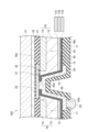
図1は、本実施形態に係る光検出装置1Aの部分断面図である。図2は、光検出装置1Aが備える半導体光検出素子(以下、単に光検出素子という)10の概略平面図である。図3は、光検出装置1Aの回路図である。
Figure 1 is a partial cross-sectional view of the
光検出装置1Aは、図1に示されるように、光検出素子10、ガラス基板31、及び搭載基板35を備えている。搭載基板35は、光検出素子10に対向配置されている。ガラス基板31は、光検出素子10に対向配置されている。光検出素子10は、搭載基板35とガラス基板31との間に配置されている。
As shown in Fig. 1, the
本実施形態の光検出素子10は、フォトダイオードアレイである。光検出素子10は、平面視において矩形状を呈する半導体基板16を有している。半導体基板16は、互いに反対を向く主面16aと裏面16bとを含んでいる。主面16aには、被検出光が入射する。一例では、半導体基板16はSi基板またはInP基板である。半導体基板16の厚さ(主面16aと裏面16bとの距離)は、例えば1μm以上1000μm以下である。
The
光検出素子10は、半導体基板16に形成された複数の光検出領域11を含んでいる。これらの光検出領域11は、被検出光の光強度に応じた量の電荷を生成する。それぞれの光検出領域11には、クエンチング抵抗21が直列に接続されている。一つの光検出領域11は、光検出素子10における一つのセルを構成している。The
各光検出領域11は、それぞれクエンチング抵抗21と直列に接続された形で、全て並列に接続されており、電源から逆バイアス電圧が印加される。光検出領域11からの出力電流は、後述する信号処理部36によって検出される。図2では、構造の明確化のため、図1に示した絶縁膜41の記載を省略している。Each
個々の光検出領域11は、第二導電型(例えばp型)の半導体領域14を有している。半導体領域14は、半導体基板16の主面16a側に形成されている。半導体領域14の平面形状は、たとえば多角形(本実施形態では、八角形)である。また、半導体基板16は、第一導電型(例えばn型)の半導体領域12を有している。半導体領域12は、半導体基板16において半導体領域14を除く領域を占める。Each
光検出領域11は、図2に示されるように、半導体基板16の主面16a側にそれぞれ配置された、電極22と電極23とを有している。電極22は、半導体領域14に電気的に接続されている。電極23は、主面16a側から見て、半導体領域14の外側の半導体基板16上に、絶縁膜41を介して形成されている。また、光検出領域11は、半導体基板16の裏面16b側にそれぞれ配置された、半導体基板16に電気的に接続された電極(図示省略)と、電極24とを有している。電極24は、半導体基板16の裏面16b上に、絶縁膜42を介して形成されている。2, the
光検出素子10は、個々の光検出領域11毎に、半導体領域14の外側の半導体基板16上に、絶縁膜41を介して形成されたクエンチング抵抗21を有している。すなわち、クエンチング抵抗21は、半導体基板16の主面16a側に配置されている。クエンチング抵抗21は、その一方端が電極22に接続され、その他方端が電極23に接続されている。クエンチング抵抗21は、これが接続される電極22よりも抵抗率が高い。クエンチング抵抗21は、たとえばポリシリコンからなる。クエンチング抵抗21の形成方法としては、CVD(Chemical Vapor Deposition)法を用いることができる。
The
光検出素子10は、複数の貫通電極26を含んでいる。貫通電極26は、個々の光検出領域11毎に設けられている。貫通電極26は、主面16aと裏面16bとの間を貫通して形成されている。すなわち、貫通電極26は、半導体基板16を貫通する貫通孔15内に配置されている。貫通孔15の内側面は、半導体基板16の厚さ方向(すなわち主面16a及び裏面16bに垂直な方向)に延びている。The
絶縁膜42は、貫通孔15内にも形成されている。貫通電極26は、絶縁膜42を挟んで、貫通孔15の内側面上及び底面上に配置されている。貫通電極26の一端は、電極23に接続され、電極23、クエンチング抵抗21、及び電極22を介して光検出領域11の半導体領域14と電気的に接続されている。貫通電極26の他端は、電極24に接続されている。The insulating
貫通電極26は、平面視において、光検出領域11間の領域に配置されている。本実施形態では、光検出領域11は、第一方向にM行、第一方向に直交する第二方向にN列(M,Nは自然数)に2次元配列されている。貫通電極26は、4つの光検出領域11に囲まれる領域に形成されている。貫通電極26は、光検出領域11毎に設けられているため、第一方向にM行、第二方向にN列に2次元配列される。The through
電極22,23,24及び貫通電極26は金属からなる。電極22,23,24及び貫通電極26に用いられる金属としては、例えば、Al、Ti、Cu、Ni、AlCuなどの単層膜、或いはAl/Ni、Al/Ti/Cu、Ti/Cu、Ti/Cu/Ni、Ti/Cu/Tiなどの積層膜が挙げられる。なお、A/B/Cとの表記は、半導体基板16側から順にA層、B層及びC層が積層されていることを意味する。The
半導体基板16がInP基板である場合には、電極材料としては、AuGe/Niなどもよく用いられる。プロセス設計にも因るが、電極24及び貫通電極26は一体に形成することができる。電極22,23,24及び貫通電極26の形成方法としては、スパッタ法を用いることができる。When the
Siを用いた場合におけるp型不純物としてはBなどの3族元素が用いられ、n型不純物としては、N、P又はAsなどの5族元素が用いられる。半導体の導電型であるn型とp型は、互いに置換して素子を構成しても、当該素子を機能させることができる。これらの不純物の添加方法としては、拡散法やイオン注入法を用いることができる。When Si is used,
絶縁膜41,42の材料としては、SiO2、SiN又はSiONといった絶縁性シリコン化合物、Al2O3又はTiO2といった絶縁性金属酸化物、或いは絶縁性樹脂を用いることができる。絶縁膜41,42の形成方法としては、絶縁膜41,42がSiO2からなる場合には、熱酸化法又はCVD法を用いることができる。
The insulating
上述の構造の場合、n型の半導体領域12とp型の半導体領域14との間に、pn接合が構成されることで、光検出領域11としてのフォトダイオード(例えばアバランシェフォトダイオード)が形成されている。半導体領域12は、裏面16b側に形成された電極(図示省略)と電気的に接続され、半導体領域14は、電極22と電気的に接続されている。クエンチング抵抗21は、光検出領域11に対して直列に接続されている(図3参照)。In the above-described structure, a pn junction is formed between the n-
各光検出領域11がアバランシェフォトダイオードである場合、個々の光検出領域11をガイガーモードで動作させる。ガイガーモードでは、光検出領域11のブレークダウン電圧よりも大きな逆方向電圧(逆バイアス電圧)を光検出領域11のアノード/カソード間に印加する。すなわち、アノードには負電位V1を、カソードには正電位V2を印加する。これらの電位の極性は相対的なものであり、一方の電位をグランド電位とすることも可能である。アノードはp型の半導体領域14であり、カソードはn型の半導体領域12である。When each
光検出領域11に被検出光の光子が入射すると、半導体基板16の内部において光電変換が行われ、光電子が発生する。半導体領域14のpn接合界面の近傍領域において、アバランシェ増倍が行われ、増幅されたキャリアは半導体基板16の主面16aに形成された電極22に向けて流れる。すなわち、光検出素子10のいずれかのセル(光検出領域11)に光子が入射すると、光電変換後に電子増倍がなされて、電流信号が電極24から取り出される。When a photon of the light to be detected is incident on the
光検出素子10は、光吸収膜13を備えている。光吸収膜13は、半導体基板16の裏面16b上に設けられ、半導体基板16の裏面16bと絶縁膜42との間に配置されている。光吸収膜13は、光検出領域11に吸収されずに透過した被検出光、及び/又は光検出領域11において発生する自発光を吸収するために設けられている。光吸収膜13は、光吸収層131、共振層132及び反射層133を含む多層構造を有する。The
光吸収層131は、共振層132と半導体基板16との間に設けられている。光吸収層131の厚さは、数nmから数μmの範囲内である。共振層132は、反射層133と半導体基板16との間、具体的には反射層133と光吸収層131との間に設けられている。共振層132の厚さは、数nmから数百μmの範囲内である。The light
一例では、共振層132の光学厚さは、被検出光の波長λ1または光検出領域11において生じる自発光の波長λ2の、4分の1の整数倍である。或いは、共振層132の光学厚さは、λ1/4又はλ2/4の整数倍を中心とする±20%の範囲内であってもよい。被検出光の波長λ1は、可視域から近赤外域の範囲内であり、例えば350nm以上1200nm以下である。光検出領域11において生じる自発光の波長λ2は、光検出領域11がアバランシェフォトダイオードである場合、例えば700nm以上1100nm以下である。反射層133の厚さは、数十nmから数mmの範囲内である。
In one example, the optical thickness of the
また、波長λ1及びλ2のうち少なくとも一方において、共振層132の内部の光透過率は、光吸収層131の内部の光透過率より大きい。言い換えると、共振層132の消衰係数は、光吸収層131の消衰係数より小さい。光吸収層131は、例えば金属により構成される。光吸収層131を構成する金属は、タングステンシリサイド(WSix)、Ti、TiN、及びCrからなる群から選択される一以上の材料を含んでもよい。一例では、光吸収層131はタングステンシリサイドを主に含み、一実施例ではタングステンシリサイドからなる。
Also, at least one of the wavelengths λ 1 and λ 2 , the optical transmittance inside the
共振層132は、例えばSiO2、SiN、SiONといったシリコン化合物を主に含み、一実施例ではSiO2、SiN、又はSiONからなる。波長λ1,λ2のうち少なくとも一方において、共振層132は光透過性を有してもよい。なお、光透過性を有するとは、対象波長に対して透明であること、すなわち70%以上の光透過率を有することをいう。
The
また、波長λ1,λ2のうち少なくとも一方において、反射層133の表面の光反射率は、共振層132の表面の光反射率より大きい。なお、本実施形態において、「反射層の表面の光反射率」とは、反射層の共振層側の表面の光反射率をいい、「共振層の表面の光反射率」とは、共振層の光吸収層側の表面の光反射率をいう。
Moreover, at least one of the wavelengths λ 1 and λ 2 , the optical reflectance of the surface of the
反射層133は、金属層である。反射層133を構成する金属は、Al、Al系合金(AlCu、AlSi等)、Cu、Ag、及びAuからなる群から選択される一以上の材料を含んでもよい。一例では、反射層133はAlを主に含み、一実施例ではAlからなる。The
図1に示されるように、搭載基板35は平坦な主面35aを有している。搭載基板35は、平面視において矩形形状を呈している。主面35aは、半導体基板16の裏面16bと対向している。搭載基板35は、主面35a上に配置された複数の電極27を含んでいる。電極27は、貫通電極26に対応して配置されている。具体的には、電極27は、主面35aにおける、電極24に対向する各領域上に形成されている。1, the mounting
電極24と電極27とは、バンプ電極25により接続されている。これにより、貫通電極26は、電極24及びバンプ電極25を介して、電極27に電気的に接続される。そして、クエンチング抵抗21は、電極23、貫通電極26、電極24、及びバンプ電極25を介して、電極27に電気的に接続される。電極27は、電極22,23,24及び貫通電極26と同様の金属からなる。バンプ電極25は、例えば半田を主に含む。
搭載基板35は、図3に示される信号処理部36を含んでいる。すなわち、搭載基板35は、ASIC(Application Specific Integrated Circuit)を構成している。各電極27は、搭載基板35内に形成された配線(図示省略)を介して信号処理部36と電気的に接続されている。信号処理部36には、各光検出領域11からの出力信号が入力され、信号処理部36は、各光検出領域11からの出力信号を処理する。The mounting
信号処理部36は、各光検出領域11からの出力信号をデジタルパルスに変換するCMOS回路を含んでいる。また、搭載基板35は、各セル(光検出領域11)に対応して、時間情報を記録する回路が含まれるように構成されている。時間情報を記録する回路としては、時間デジタル変換器(TDC:Time to Digital Convertor)、又は、時間電圧変換器(TAC:Time to Amplitude Convertor)などが用いられる。これにより、搭載基板35内での配線距離の差は、時間分解能に影響を与えない。The
半導体基板16の裏面16b上には、バンプ電極25に対応する位置に開口43aが形成されたパッシベーション膜43が配置されている。搭載基板35の主面35a上には、バンプ電極25に対応する位置に開口44aが形成されたパッシベーション膜44が配置されている。A
パッシベーション膜43,44は、例えば、ポリイミド系、フェノール系、エポキシ系等の樹脂絶縁膜、SiO2/樹脂絶縁膜、SiN/樹脂絶縁膜、SiON/樹脂絶縁膜、SiO2膜、SiN膜、又はSiON膜からなる。パッシベーション膜43,44の形成方法としては、樹脂絶縁膜の場合にはスピンコート法を用いることができ、SiO2膜の場合にはCVD(Chemical Vapor Deposition)法を用いることができる。
The
ガラス基板31は、互いに反対を向く主面31aと裏面31bとを有している。ガラス基板31は、平面視において矩形状を呈している。裏面31bは、半導体基板16の主面16aと対向している。主面31a及び裏面31bは平坦である。ガラス基板31と光検出素子10とは、光学接着剤32により接着され、且つ光学的に接続されている。ガラス基板31は、光検出素子10上に直接形成されていてもよい。The
ガラス基板31の主面31a上には、別の光学接着剤を介してシンチレータ(不図示)が光学的に接続されてもよい。シンチレータからのシンチレーション光は、被検出光として、ガラス基板31を透過し、光検出素子10に入射する。A scintillator (not shown) may be optically connected via another optical adhesive to the
次に、図4~図7を参照して、上述した光検出装置1Aの製造方法を説明する。図4~図7は、本実施形態に係る光検出装置1Aの製造過程を説明するための図である。Next, a method for manufacturing the above-mentioned
まず、図4(a)に示されるように、半導体領域12及び14を有する半導体基板16を作製する。この工程では、例えば、第一導電型の半導体基板を用意し、この半導体基板の主面側からイオン注入を行うことにより、第二導電型の半導体領域14を複数形成する。このとき、半導体領域14を除く他の領域が半導体領域12となる。First, as shown in Fig. 4(a), a
次に、図4(b)に示されるように、半導体基板16の主面16a上に、クエンチング抵抗21、電極22及び23、並びに絶縁膜41を形成する。この工程では、まず、絶縁膜41の下層部分を形成する。その後、絶縁膜41の下層部分のうち半導体領域14上に位置する部分に開口を形成したのち、絶縁膜41の下層部分上にクエンチング抵抗21、電極22及び23を形成する。このとき、電極22は開口を介して半導体領域14と接続する。そして、絶縁膜41の上層部分を形成し、この上層部分によりクエンチング抵抗21、電極22及び23を覆う。
Next, as shown in FIG. 4(b), the quenching
続いて、図4(c)に示されるように、光学接着剤32を間に挟んでガラス基板31と絶縁膜41とを互いに接着する。これにより、ガラス基板31と光検出素子10とが光学的に接続される。続いて、半導体基板16の裏面16bを研磨して半導体基板16を薄化する。この工程では、例えば、機械研磨法又は化学研磨法を用いて半導体基板16を薄化する。4(c), the
そして、図5(a)に示されるように、半導体基板16の裏面16b上に、光吸収膜13を形成する。一例では、光吸収層131(例えばWSix)をスパッタにより形成し、共振層132(例えばSiO2)をCVDにより形成し、反射層133(例えばAlCu)をスパッタにより形成する。
5A, the
続いて、図5(b)に示されるように、光吸収膜13及び半導体基板16に貫通孔15を形成する。この工程では、例えば、ドライエッチング法とウエットエッチング法とを適宜選択して貫通孔15を形成し、電極23が露出した時点でエッチングを停止する。なお、貫通孔15を形成したのち、光吸収膜13を形成してもよい。5(b), through
続いて、図5(c)に示されるように、半導体基板16の裏面16b上(光吸収膜13上)、並びに貫通孔15の内側面上及び底面上(電極23上)に、絶縁膜42を形成する。そして、図6(a)に示されるように、絶縁膜42のうち貫通孔15の底面上(電極23上)に位置する部分に、開口42aを形成する。この工程では、開口42aを、例えば電極23が露出するまで絶縁膜42をエッチングすることにより形成する。5(c), an insulating
続いて、図6(b)に示されるように、貫通孔15の内側面上及び底面上、並びに裏面16bのうち貫通孔15の周囲に位置する領域上に、金属膜を形成する。これにより、貫通孔15の内側面上及び底面上に貫通電極26が形成されるとともに、裏面16b上に電極24が形成される。6(b), a metal film is then formed on the inner and bottom surfaces of the through
続いて、図7(a)に示されるように、半導体基板16の裏面16b上及び貫通孔15内にパッシベーション膜43を形成し、パッシベーション膜43により電極24及び貫通電極26を覆う。そして、図7(b)に示されるように、パッシベーション膜43のうち電極24上に位置する部分に、開口43aをエッチングにより形成する。その後、開口43aを覆うバンプ電極25を形成する。7(a), a
なお、バンプ電極25の形成に先立って、電極24におけるパッシベーション膜43から露出する領域に、UBM(Under Bump Metal)を形成する。UBMは、バンプ電極25と電気的及び物理的に接続が優れた材料からなる。UBMの形成方法としては、無電解めっき法を用いることができる。バンプ電極25の形成方法としては、ハンダボールを搭載する手法又は印刷法を用いることができる。Prior to forming the
続いて、光検出素子10と、別途用意した搭載基板35とを互いにバンプ接続する(図1を参照)。そして、ガラス基板31、光検出素子10、及び搭載基板35からなる積層体をダイシングにより切断し、個片化する。以上の工程を経て、本実施形態の光検出装置1Aが作製される。なお、ガラス基板31と光検出素子10とからなる積層体をダイシングにより個片化した後に、その積層体の光検出素子10と搭載基板35とを互いにバンプ接続してもよい。Next, the
以上に説明した本実施形態の光検出素子10によって得られる作用効果について説明する。本実施形態の光検出素子10では、半導体基板16の主面16aから入射した被検出光の光強度に応じた量の電荷が、光検出領域11において生成される。これにより、被検出光の入射光量を電気的に検出することができる。光検出領域11において吸収されなかった被検出光は、半導体基板16の裏面16b上に設けられた光吸収膜13に達する。光検出領域11において自発光が生じた場合には、その自発光も同様に、光吸収膜13に達する。The effects obtained by the
光吸収膜13は、光吸収層131、共振層132、及び反射層133を含む多層構造を有する。光吸収膜13に入射した光の一部は、光吸収層131において直ちに吸収される。光吸収層131に吸収されなかった光は光吸収層131を通過し、共振層132に入る。そして、共振層132に入った光は、光吸収層131及び共振層132の界面と、共振層132及び反射層133の界面との間で多重反射しつつ、光吸収層131において徐々に吸収される。The
したがって、この光吸収膜13によれば、単層の光吸収膜と比較して、極めて高い吸収効率を実現できる。故に、本実施形態の光検出素子10によれば、半導体基板16の裏面16bにおける光の反射を効果的に低減できるので、時間分解能の低下を抑制し、また隣接セル間のクロストークを低減することができる。Therefore, this
前述したように、共振層132の光学厚さは、被検出光の波長λ1または光検出領域11において生じる自発光の波長λ2の4分の1(すなわちλ1/4またはλ2/4)の整数倍を中心とする±20%の範囲内であってもよい。
As described above, the optical thickness of the
この場合、光吸収層131及び共振層132の界面にて反射した光の位相と、共振層132及び反射層133の界面にて反射した光の位相とが互いにπ(rad)近くずれるので、互いに打ち消し合う。したがって、光吸収膜13の吸収効率(消衰効率)を更に高めることができる。In this case, the phase of the light reflected at the interface between the light absorbing
前述したように、光検出領域11は、アバランシェフォトダイオードまたはpn接合型フォトダイオードであってもよい。例えばこのような場合に、被検出光の光強度に応じた量の電荷を光検出領域11において生成することができる。As mentioned above, the
また、特に光検出領域11がアバランシェフォトダイオードである場合には、光検出領域11において自発光(2次フォトン)が生じる。本実施形態の光検出素子10は、光吸収膜13を適宜設計することにより、光検出領域11において生じる自発光によるクロストークをも低減することができる。したがって、本実施形態の光検出素子10は、光検出領域11がアバランシェフォトダイオードである場合に特に有効である。Furthermore, particularly when the
本実施形態のように、光検出素子10は、主面16aと裏面16bとの間を貫通し、主面16a側の一端が光検出領域11と電気的に接続された貫通電極26を備えてもよい。この場合、被検出光が入射する主面16aとは反対側の裏面16bに搭載基板35を配置することができ、多数の光検出領域11が主面16aにおいて二次元状に並んでいる場合であっても、各光検出領域11からの電荷(出力電流)を容易に取り出すことができる。As in this embodiment, the
また、搭載基板35と電気的に接続するためのボンディングワイヤ等の配線を主面16a側に設ける必要がないので、光検出素子10のフィルファクタを増大することができる。言い換えると、光検出素子10のサイズを小型化することができ、小型のパッケージ内に収容することが可能になる。
In addition, since there is no need to provide wiring such as bonding wires on the
また、貫通電極26の形成容易性を高める為には、半導体基板16を薄くするとよい(図5(a)を参照)。しかし、そうすると半導体基板16の光入射面(主面16a)と裏面16bとの距離が短くなるので、時間分解能の低下及び隣接セル間のクロストークが生じ易くなる。本実施形態の光検出素子10によれば、時間分解能の低下を抑制し、また隣接セル間のクロストークを低減できるので、半導体基板16に貫通電極26を設ける場合に特に有効である。In addition, in order to make it easier to form the through
本実施形態のように、光検出素子10はガラス基板31に接合されていてもよい。この場合、半導体基板16の機械的強度をより低くすることが許容されるので、半導体基板16をより薄くすることが可能になる。したがって、貫通孔15の形成が容易になるとともに、光検出素子10の応答特性が向上する。As in this embodiment, the
本実施形態によるクロストーク低減効果を検証した実施例について説明する。図8及び図9は、検証のために作製した積層体100A及び100Bの断面構造を模式的に示す図である。We will now describe an example in which the crosstalk reduction effect of this embodiment was verified. Figures 8 and 9 are schematic diagrams showing the cross-sectional structures of the
図8に示されるように、積層体100Aは、サポートガラス101上に、接合樹脂102、AlとCuの合金層103、CVD法により成膜したSiO2層104、WSi層105、Si層106、及びSiO2層107をこの順に積層した構造を有する。WSi層105、SiO2層104、及び合金層103は、それぞれ本実施形態の光吸収層131、共振層132、及び反射層133に相当する。Si層106は本実施形態の半導体基板16に相当する。図9に示されるように、積層体100Bは、サポートガラス101上に、接合樹脂102、AlとCuの合金層103、樹脂絶縁層108(フェノール系樹脂)、Si層106、及びSiO2層107をこの順に積層した構造を有する。
As shown in Fig. 8, the
これらの積層体100A及び100Bにおいて、サポートガラス101の厚さを300μm、接合樹脂102の厚さを10μm、合金層103の厚さを1000nm、SiO2層104の厚さを100nm、WSi層105の厚さを23nm、樹脂絶縁層108の厚さを5000nmとした。そして、Si層106の厚さを20μm~70μmの範囲内で変化させて、積層体100A及び100Bそれぞれについて複数個のサンプルを作製した。
In these
また、各積層体のSi層106に、26行26列に二次元配列された複数のセル(光検出領域)としての半導体領域110及び配線(図示せず)を形成した。半導体領域110は本実施形態の半導体領域14に相当する。各セルのサイズを一辺50μmとした。そして、それぞれのセルにクエンチング抵抗を形成し、電荷をまとめて出力する構成とした。出力された電荷を広帯域アンプにより電圧信号に変換し、コンパレータにより閾値以上の高さのパルスを抽出して、パルスの数をカウンタ回路によりカウントした。In addition, a
図10は、クロストークを含む電圧信号波形を模式的に示すグラフである。上記の各サンプルにおいて1つの光子が検出されると、1光子分の高さを有するパルス信号G12が出力される。ここで、1光子分のパルス高さを1 photon equivalent(p.e.)と定義する。隣接セル間でクロストークが生じると、電圧信号波形には、1光子分の高さを有するパルス信号G12に加えて、2光子分(或いはそれ以上)の高さを有するパルス信号G11が現れる。 Figure 10 is a graph showing a schematic diagram of a voltage signal waveform including crosstalk. When one photon is detected in each of the above samples, a pulse signal G12 having a height of one photon is output. Here, the pulse height of one photon is defined as one photon equivalent (p.e.). When crosstalk occurs between adjacent cells, in addition to the pulse signal G12 having a height of one photon, a pulse signal G11 having a height of two photons (or more) appears in the voltage signal waveform.
電圧信号に対するコンパレータの閾値を例えば0.5p.e.に設定すると(図中の直線D1)、これらのパルス信号G11,G12は、互いに区別されることなく、それぞれ1個のパルスとしてカウントされる。また、電圧信号に対するコンパレータの閾値を例えば1.5p.e.に設定すると(図中の直線D2)、パルス信号G12は検出されず、パルス信号G11のみがカウントされる。If the threshold of the comparator for the voltage signal is set to, for example, 0.5 p.e. (straight line D1 in the figure), these pulse signals G11 and G12 are not distinguished from each other and are counted as one pulse each. Also, if the threshold of the comparator for the voltage signal is set to, for example, 1.5 p.e. (straight line D2 in the figure), the pulse signal G12 is not detected and only the pulse signal G11 is counted.
図11は、サンプルを暗箱の中に配置し、コンパレータの閾値を変化させて自発光のカウントレート(以下、ダークカウントレートという)を測定した例を示すグラフである。図11において、縦軸はダークカウントレート(単位:cps(counts per second))を表し、横軸は閾値(単位:V)を表す。 Figure 11 is a graph showing an example of measuring the self-luminous count rate (hereinafter referred to as the dark count rate) by placing a sample in a dark box and changing the threshold value of the comparator. In Figure 11, the vertical axis represents the dark count rate (unit: cps (counts per second)) and the horizontal axis represents the threshold value (unit: V).
閾値が1.0(p.e.)未満となる範囲A1においては、全てのパルス高さのパルス信号がカウントされ、ダークカウントレートは高い値となる。そして、閾値が1.0(p.e.)より大きく2.0(p.e.)未満となる範囲A2においては、1.0(p.e.)の高さのパルス信号がカウントされないので、ダークカウントレートは範囲A1から一段階低くなる。こうして、閾値の増大に応じてダークカウントレートは段階的に減少する。In range A1, where the threshold is less than 1.0 (p.e.), pulse signals of all pulse heights are counted, and the dark count rate is a high value. In range A2, where the threshold is greater than 1.0 (p.e.) and less than 2.0 (p.e.), pulse signals with a height of 1.0 (p.e.) are not counted, and the dark count rate is one step lower than range A1. In this way, the dark count rate decreases in stages as the threshold increases.
範囲A1におけるダークカウントレートをN0.5p.e.、範囲A2におけるダークカウントレートをN1.5p.e.とすると、クロストークの程度を表すクロストーク確率は、N0.5p.e.とN1.5p.e.との比(N1.5p.e./N0.5p.e.)により算出される。このクロストーク確率が大きいほど、クロストークの程度が大きいといえる。 If the dark count rate in range A1 is N0.5pe and the dark count rate in range A2 is N1.5pe , the crosstalk probability, which indicates the degree of crosstalk, is calculated from the ratio of N0.5pe to N1.5pe ( N1.5pe / N0.5pe ).The higher this crosstalk probability, the greater the degree of crosstalk.
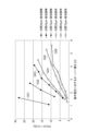
図12は、実施例の各サンプルにおける逆バイアス電圧とクロストーク確率との関係を示すグラフである。図12において、縦軸はクロストーク確率(単位:%)を表し、横軸は動作電圧に対するオーバー電圧(単位:V)を表す。図中のグラフG21~G23は、上記の積層体100B(すなわち光吸収膜なし)の場合を示し、図中のグラフG24~G26は、上記の積層体100A(すなわち光吸収膜あり)の場合を示す。また、グラフG21,G24はSi層106の厚さを20μmとした場合を示し、グラフG22,G25はSi層106の厚さを45μmとした場合を示し、グラフG23,G26はSi層106の厚さを70μmとした場合を示す。
Figure 12 is a graph showing the relationship between reverse bias voltage and crosstalk probability in each sample of the embodiment. In Figure 12, the vertical axis represents the crosstalk probability (unit: %), and the horizontal axis represents the overvoltage (unit: V) relative to the operating voltage. Graphs G21 to G23 in the figure show the case of the above-mentioned
図12を参照すると、Si層106が薄いほど、クロストーク確率が大きいことがわかる。このことは、半導体基板16が薄いほどクロストークが生じ易いことを意味する。また、図12を参照すると、積層体100A(光吸収膜あり)においては、積層体100B(光吸収膜なし)と比較して、クロストーク確率が格段に小さいことがわかる。このことは、本実施形態において、光検出素子10が光吸収膜13を備えることにより、クロストークを格段に低減できることを意味する。なお、この結果は自発光に関するものであるが、被検出光に対しても同様であると考えられる。
Referring to FIG. 12, it can be seen that the thinner the
図13は、実施例の各サンプルにおける、自発光に起因する暗電流特性を示すグラフである。図13において、縦軸は暗電流の大きさ(単位:A)を表し、横軸は逆バイアス電圧(単位:V)を表す。図中のグラフG31~G33は、上記の積層体100B(光吸収膜なし)の場合を示し、図中のグラフG34~G36は、上記の積層体100A(光吸収膜あり)の場合を示す。また、グラフG31,G34はSi層106の厚さを20μmとした場合を示し、グラフG32,G35はSi層106の厚さを45μmとした場合を示し、グラフG33,G36はSi層106の厚さを70μmとした場合を示す。
Figure 13 is a graph showing the dark current characteristics due to spontaneous light emission in each sample of the embodiment. In Figure 13, the vertical axis represents the magnitude of the dark current (unit: A), and the horizontal axis represents the reverse bias voltage (unit: V). Graphs G31 to G33 in the figure show the case of the above-mentioned
図13を参照すると、Si層106が薄いほど、使用可能な逆バイアス電圧の範囲が狭い(暗電流が急激に増大するときの逆バイアス電圧が小さい)ことがわかる。このことは、半導体基板16が薄いほど、使用可能な逆バイアス電圧の範囲が狭いことを意味する。また、図13を参照すると、積層体100A(光吸収膜あり)においては、積層体100B(光吸収膜なし)と比較して、使用可能な逆バイアス電圧の範囲が広い(暗電流が急激に増大するときの逆バイアス電圧が大きい)ことがわかる。
Referring to FIG. 13, it can be seen that the thinner the
例えば、グラフG31とグラフG34とを比較すると、Si層106の厚さが同じであっても、グラフG31では57.5V付近で暗電流が増大するが、グラフG34では61V付近で暗電流が増大する。故に、グラフG34では、グラフG31と比較して、使用可能な逆バイアス電圧の範囲が+3.5V程度広い。このことは、本実施形態において、光検出素子10が光吸収膜13を備えることにより、自発光を効果的に吸収して使用可能な逆バイアス電圧の範囲を拡大できることを意味する。For example, when comparing graph G31 and graph G34, even if the thickness of the
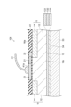
本実施形態の光吸収膜13の作用について、詳細に説明する。図14は、光吸収膜13の断面構造を模式的に示す図である。The function of the
前述したように、光吸収膜13は、光吸収層131、共振層132、及び反射層133を含む多層構造を有する。光吸収膜13に到達した光Lの一部は光吸収層131の表面において反射し、残部が光吸収層131の内部に入る。このとき、光吸収層131のシート抵抗を隣接する半導体基板16の空間インピーダンスに一致させておけば、表面反射率はゼロとなり、光吸収層131の内部に全ての光Lが入ることになる。As described above, the
光吸収層131の内部に入った光Lは、光吸収層131の消衰係数に基づいて計算される比率で次第に吸収されるので、光吸収層131が十分に厚ければ、ほとんどの光Lが光吸収層131に吸収される。しかし、光吸収層131を厚くすることは、すなわちシート抵抗を小さくすることに繋がり、光吸収層131の表面反射率が増大することとなる。したがって、本実施形態では、光吸収層131の厚みを制限し、一部の光Lが光吸収層131を通り抜けることを許容する。
The light L that enters the
この通り抜けた光Lの一部は、共振層132と光吸収層131との界面にて反射し、光吸収層131へ戻る。以下、この反射光を第一反射光と称する。光吸収層131が金属からなり、共振層132が誘電体からなる場合、共振層132のインピーダンスは光吸収層131のインピーダンスより大きい(換言すると、共振層132の屈折率は光吸収層131の屈折率より小さい)ので、第一反射光は、π(rad)の位相ずれを伴わない。A portion of the light L that passes through is reflected at the interface between the
また、光Lの残部は、該界面を通過して共振層132の内部に入る。共振層132の内部に入った光Lは、ほとんど減衰されることなく共振層132と反射層133との界面に達し、該界面において全反射する。以下、この反射光を第二反射光と称する。第二反射光は再び共振層132内部を進んで光吸収層131へ向かう。反射層133のインピーダンスは0Ωに近い(言い換えると、屈折率が無限大に近い)ので、第二反射光は、π(rad)の位相ずれを伴う。
The remaining part of the light L passes through the interface and enters the inside of the
第二反射光が光吸収層131に到達したときに、第二反射光と第一反射光との位相差がπ(rad)であれば、互いに打ち消し合う。その為には、共振層132の光学厚さ(換言すると、光吸収層131と反射層133との光学的間隔)が、光Lの波長の1/4であればよい。但し、第一反射光の電界振幅と第二反射光の電界振幅とは全く同じではないので、完全には打ち消し合わず、反射光の一部は光吸収層131に入射する。光吸収層131に入射した反射光は、光吸収層131において吸収される。また、第二反射光の一部は共振層132の内部に残り、多重反射を繰り返すが、徐々に光吸収層131に吸収される。こうして、光Lのほとんどが光吸収層131に吸収されることとなる。When the second reflected light reaches the
光吸収膜13の設計例について説明する。図15は、半導体基板16の裏面16b上に光吸収膜13を配置した構成を模式的に示す図である。We will explain a design example of the
本実施形態では、図15に示されるように、光吸収膜13の光吸収層131が半導体基板16に接している。ここでは、半導体基板16はSi又はInPからなるものとする。光Lの波長は1.55μmであるものとする。光吸収層131はWSiからなり、共振層132はSiO2からなり、反射層133はAlからなるものとする。
In this embodiment, as shown in Fig. 15, the
空気の特性インピーダンスは377Ωであり、Si及びInPの屈折率は約3.5であるから、半導体基板16の特性インピーダンスは377Ω/3.5=108Ωとなる。また、タングステンシリサイド(WSi2)の比抵抗は2.48×10-4Ω・cmである。したがって、光吸収層131の好適な厚みtは、

また、SiO2の比屈折率は1.48であるから、共振層132の好適な厚さは、1.55μm/1.48/4=262nmとして算出される。また、Alの比抵抗は2.65×10-6Ω・cmであるから、反射層133を例えば1μmといった十分な厚みとすることにより、シート抵抗は0.0265Ωとなる。SiO2のインピーダンスは

上記の考え方に従えば、被検出光の波長λ1、又は自発光の波長λ2に応じた光吸収膜13の設計も容易となる。下記の表1は、被検出光の波長λ1が600nm、800nm、及び1000nmである場合における光吸収膜13の設計例を示す表である。また、下記の表2は、自発光の波長λ2が700nm~1100nmの範囲内である場合における光吸収膜13の設計例を示す表である。


なお、上記の設計例では、光吸収膜13の表面に対して垂直な方向(言い換えると、光吸収膜13の厚み方向)から光Lが入射することを想定しているが、光吸収膜13の表面に対して傾斜した方向から光Lが入射する場合には、上記の設計に光Lの入射角を加味するとよい。すなわち、各層131~133の屈折率から各層131~133内における光の伝搬角度を計算し、各層131~133の厚さを、この伝搬角度を考慮した厚さとするとよい。In the above design example, it is assumed that light L is incident from a direction perpendicular to the surface of the light absorbing film 13 (in other words, the thickness direction of the light absorbing film 13), but if light L is incident from a direction inclined to the surface of the
(変形例)(Variation)
図16は、上記実施形態の第1変形例に係る光検出素子10Aの構造を示す部分断面図である。この光検出素子10Aは、ガラス基板31及び光学接着剤32を備えない点において上記の光検出素子10と相違し、その他の点において光検出素子10と一致する。このような構造であっても、上記実施形態と同様の作用効果を奏することができる。
Figure 16 is a partial cross-sectional view showing the structure of a
また、本変形例のようにガラス基板31が設けられない場合、ガラス基板31及び光学接着剤32による光損失(吸収及び反射)を回避でき、光検出効率を高めることができる。加えて、光学接着剤32からのアウトガスの発生を回避できる。更には、シンチレータ又はマイクロレンズといった追加の光学部品を、光検出素子の光入射面に直接搭載することが可能になる。
Furthermore, when the
図17は、上記実施形態の第2変形例に係る光検出素子10Bの構造を示す部分断面図である。この光検出素子10Bは、光吸収膜13が裏面16b上に加えて貫通孔15の内側面上及び底面上にも形成されている点において上記の光検出素子10と相違し、その他の点において光検出素子10と一致する。この場合、絶縁膜42及び貫通電極26は、光吸収膜13を介して、貫通孔15内に配置される。
Figure 17 is a partial cross-sectional view showing the structure of a
このような構造であれば、裏面16bに加えて貫通孔15の内側面における光の反射を抑制できるので、時間分解能の低下を更に抑制し、また隣接セル間のクロストークを更に低減できる。本変形例の光検出素子10Bを作製する際には、貫通孔15を形成したのちに光吸収膜13を形成するとよい。なお、上記実施形態のように、光吸収膜13が裏面16bのみに形成され、貫通孔15の内側面上及び底面上には形成されない場合、製造工程が容易になり、工数を削減して低コスト化できるという利点がある。
With this structure, reflection of light on the inner surface of the through
図18は、上記実施形態の第3変形例に係る光検出素子10Cの構造を示す部分断面図である。この光検出素子10Cは、ガラス基板31及び光学接着剤32を備えない点において上記の光検出素子10Bと相違し、その他の点において光検出素子10Bと一致する。このような構造によれば、第1変形例及び第2変形例と同様の作用効果を奏することができる。
Figure 18 is a partial cross-sectional view showing the structure of a
図19は、上記実施形態の第4変形例に係る光検出素子10Dの構造を示す部分断面図である。この光検出素子10Dは、貫通孔15の内側面が、半導体基板16の厚さ方向(すなわち主面16a及び裏面16bに垂直な方向)に対して傾斜している点において上記の光検出素子10と相違し、その他の点において光検出素子10と一致する。この場合、貫通孔15の内径は、主面16aから裏面16bへ近づくにしたがって拡大する。このような構造であっても、上記実施形態と同様の作用効果を奏することができる。
Figure 19 is a partial cross-sectional view showing the structure of a
図20は、上記実施形態の第5変形例に係る光検出素子10Eの構造を示す部分断面図である。この光検出素子10Eは、ガラス基板31及び光学接着剤32を備えない点において上記の光検出素子10Dと相違し、その他の点において光検出素子10Dと一致する。このような構造であっても、上記実施形態と同様の作用効果を奏することができる。また、ガラス基板31が設けられないことにより、第1変形例と同様の作用効果を奏することができる。
Figure 20 is a partial cross-sectional view showing the structure of a
図21は、上記実施形態の第6変形例に係る光検出素子10Fの構造を示す部分断面図である。この光検出素子10Fは、光吸収膜13が裏面16b上に加えて貫通孔15の内側面上及び底面上にも形成されている点において上記の光検出素子10Dと相違し、その他の点において光検出素子10Dと一致する。この場合、第2変形例と同様の作用効果を奏することができる。21 is a partial cross-sectional view showing the structure of a
図22は、上記実施形態の第7変形例に係る光検出素子10Gの構造を示す部分断面図である。この光検出素子10Gは、ガラス基板31及び光学接着剤32を備えない点において上記の光検出素子10Fと相違し、その他の点において光検出素子10Fと一致する。このような構造によれば、第5変形例及び第6変形例と同様の作用効果を奏することができる。22 is a partial cross-sectional view showing the structure of a
図23は、上記実施形態の第8変形例に係る光検出素子10Hの構造を示す部分断面図である。この光検出素子10Hは、上記実施形態のバンプ電極25及び貫通電極26に代えてボンディングワイヤ28を備えており、また、上記実施形態のガラス基板31及び光学接着剤32に代えてガラス基板33及び光学接着剤34を備えている。23 is a partial cross-sectional view showing the structure of a
具体的には、半導体基板16には貫通孔15が形成されておらず、電極23は、絶縁膜41の上面に形成された開口41aを通じて露出している。ボンディングワイヤ28は、複数のセルそれぞれに設けられている。そして、ボンディングワイヤ28の一端は、開口41aにおいて露出した電極23の部分と接続している。なお、ボンディングワイヤ28の他端は、上記実施形態の搭載基板35と同様の回路を有する図示しない回路基板と接続している。Specifically, no through-
光吸収膜13は、半導体基板16の裏面16bの全面にわたって形成されており、半導体基板16とは反対側の光吸収膜13の面(すなわち、反射層133の表面)には、光学接着剤34を介してガラス基板33が接着されている。このような構造であっても、上記実施形態と同様の作用効果を奏することができる。また、貫通電極26を形成する必要がないので、製造工程が容易になり、工数を削減して低コスト化できる。The
図24は、上記実施形態の第9変形例に係る光検出素子10Jの構造を示す部分断面図である。この光検出素子10Jは、ガラス基板33及び光学接着剤34を備えない点において上記の光検出素子10Hと相違し、その他の点において光検出素子10Hと一致する。このような構造であっても、第8変形例と同様の作用効果を奏することができる。また、ガラス基板33が設けられないことにより、第1変形例と同様の作用効果を奏することができる。
Figure 24 is a partial cross-sectional view showing the structure of a
半導体光検出素子は、上記実施形態及び構成例に限定されるものではなく、種々の変形が可能である。The semiconductor photodetector element is not limited to the above embodiments and configuration examples, and various modifications are possible.
一つの貫通電極26には、一つのクエンチング抵抗21が電気的に接続されているが、これに限られない。一つの貫通電極26に、複数のクエンチング抵抗(たとえば、4つのクエンチング抵抗)21が電気的に接続されていてもよい。この場合、セル間で貫通電極26の共通化が図られ、半導体基板16に形成される貫通電極26の数を低減できる。これにより、半導体基板16の機械的強度の低下を抑制することができる。一つの貫通電極26に、電気的に接続されるクエンチング抵抗の数は、「4」に限られることなく、「3」以下でもよく、また、「5」以上でもよい。One
一つの貫通電極26に複数のクエンチング抵抗21が電気的に接続されている場合、各光検出領域11から対応するクエンチング抵抗21を介した貫通電極26までの配線距離が同等であることが好ましい。この場合、セル間で貫通電極26の共通化が図られた構成においても、時間分解能が低下するのを防ぐことができる。When
半導体領域14の形状は、上述した形状に限られることなく、他の形状(たとえば、円形状など)であってもよい。また、光検出領域11の数(行数及び列数)や配列は、上述したものに限られない。The shape of the
光検出素子10は、複数の光検出領域11を備えているが、これに限られない。光検出素子は、単一の光検出領域11を備えてもよい。その場合であっても、時間分解能の低下を抑制する効果を奏することができる。The
光検出装置1Aは、複数の光検出領域11からの出力電流をまとめて(一括して)出力する構成を備えているが、これに限られない。光検出素子は、複数の光検出領域11(画素)からの出力電流を光検出領域11毎に個別に出力する光検出装置に適用されてもよい。そのような光検出装置は、例えばCCDなどの撮像装置として利用できる。その場合、上記実施形態の「セル」は「画素」に読み替えられ、光検出素子は隣接画素間のクロストークを低減できる。The
上記実施形態による半導体光検出素子は、被検出光が入射する主面、及び主面とは反対を向く裏面を有し、被検出光の光強度に応じた量の電荷を生成する一又は複数の光検出領域を主面側に有する半導体基板と、半導体基板の裏面上に設けられた光吸収膜と、を備え、光吸収膜は、金属層である反射層と、反射層と半導体基板との間に設けられた共振層と、共振層と半導体基板との間に設けられた光吸収層と、を含む多層構造を有し、被検出光の波長及び光検出領域において生じる自発光の波長のうち少なくとも一方において、共振層の内部の光透過率は光吸収層の内部の光透過率より大きく、反射層の表面の光反射率は共振層の表面の光反射率より大きい構成としている。The semiconductor photodetector element according to the above embodiment comprises a semiconductor substrate having a main surface on which the light to be detected is incident and a back surface facing away from the main surface, the semiconductor substrate having one or more photodetection regions on the main surface side that generate an amount of charge according to the intensity of the light to be detected, and a light absorbing film provided on the back surface of the semiconductor substrate, the light absorbing film having a multilayer structure including a reflective layer which is a metal layer, a resonant layer provided between the reflective layer and the semiconductor substrate, and a light absorbing layer provided between the resonant layer and the semiconductor substrate, and configured such that for at least one of the wavelengths of the light to be detected and the wavelengths of the spontaneous emission generated in the light detection region, the optical transmittance inside the resonant layer is greater than the optical transmittance inside the light absorbing layer, and the optical reflectance of the surface of the reflective layer is greater than the optical reflectance of the surface of the resonant layer.
上記の半導体光検出素子において、共振層の光学厚さは、被検出光の波長の4分の1及び自発光の波長の4分の1のうちいずれか一方の整数倍を中心とする±20%の範囲内である構成としてもよい。In the above semiconductor photodetector element, the optical thickness of the resonant layer may be configured to be within a range of ±20% centered on an integer multiple of either one-quarter of the wavelength of the detected light or one-quarter of the wavelength of the spontaneous emission.
この場合、光吸収層及び共振層の界面にて反射した光の位相と、共振層及び反射層の界面にて反射した光の位相とが互いにπ(rad)近くずれるので、互いに打ち消し合う。したがって、光吸収膜の吸収効率(消衰効率)を更に高めることができる。In this case, the phase of the light reflected at the interface between the light absorbing layer and the resonant layer and the phase of the light reflected at the interface between the resonant layer and the reflective layer are shifted by nearly π (rad), so they cancel each other out. This further increases the absorption efficiency (extinction efficiency) of the light absorbing film.
上記の半導体光検出素子において、一又は複数の光検出領域は、アバランシェフォトダイオードまたはpn接合型フォトダイオードである構成としてもよい。例えばこのような場合に、被検出光の光強度に応じた量の電荷を光検出領域において生成することができる。In the above-mentioned semiconductor photodetector element, one or more of the photodetection regions may be configured as an avalanche photodiode or a pn junction photodiode. In such a case, for example, an amount of charge corresponding to the light intensity of the detected light can be generated in the photodetection region.
また、特に光検出領域がアバランシェフォトダイオードである場合には、光検出領域において自発光が生じる。上記の半導体光検出素子では、光検出領域において生じる自発光によるクロストークをも低減することができる。したがって、上記の半導体光検出素子は、光検出領域がアバランシェフォトダイオードである場合に特に有効である。 In particular, when the light detection region is an avalanche photodiode, spontaneous light emission occurs in the light detection region. The above-mentioned semiconductor light detection element can also reduce crosstalk caused by spontaneous light emission in the light detection region. Therefore, the above-mentioned semiconductor light detection element is particularly effective when the light detection region is an avalanche photodiode.
上記の半導体光検出素子は、主面と裏面との間を貫通し、主面側の一端が光検出領域と電気的に接続された貫通電極を更に備える構成としてもよい。この場合、光が入射する主面とは反対側の裏面に配線基板等を配置することができ、多数の光検出領域が主面に並んでいる場合であっても、各光検出領域からの電荷(出力電流)を容易に取り出すことができる。The semiconductor photodetector element may further include a through electrode that penetrates between the main surface and the back surface and has one end on the main surface electrically connected to the photodetection region. In this case, a wiring board or the like can be disposed on the back surface opposite the main surface where light is incident, and even when multiple photodetection regions are arranged on the main surface, the charge (output current) from each photodetection region can be easily extracted.
また、貫通電極の形成容易性を高める為には、半導体基板を薄くするとよい。しかし、そうすると半導体基板の光入射面(主面)と裏面との距離が短くなるので、時間分解能の低下及び隣接画素間(隣接セル間)のクロストークが生じ易くなる。上記の半導体光検出素子によれば、時間分解能の低下を抑制し、また隣接画素間(隣接セル間)のクロストークを低減できるので、半導体基板に貫通電極を設ける場合に特に有効である。 In addition, to make it easier to form the through electrodes, it is advisable to make the semiconductor substrate thinner. However, doing so shortens the distance between the light incident surface (main surface) and the back surface of the semiconductor substrate, which makes it easier for a decrease in time resolution and crosstalk between adjacent pixels (adjacent cells) to occur. The above-mentioned semiconductor photodetector element can suppress the decrease in time resolution and reduce crosstalk between adjacent pixels (adjacent cells), making it particularly effective when providing a through electrode in the semiconductor substrate.
上記の半導体光検出素子において、光吸収層はタングステンシリサイドを主に含み、共振層はSiO2を主に含む構成としてもよい。この場合、吸収効率が高い光吸収膜を実現することができる。 In the above-mentioned semiconductor photodetector element, the light absorption layer may mainly contain tungsten silicide, and the resonance layer may mainly contain SiO 2. In this case, a light absorption film with high absorption efficiency can be realized.
本発明は、半導体基板の裏面における光の反射を低減できる半導体光検出素子として利用可能である。 The present invention can be used as a semiconductor photodetector element that can reduce light reflection on the back surface of a semiconductor substrate.
1A…光検出装置、10,10A~10H,10J…光検出素子、11…光検出領域、12…半導体領域、13…光吸収膜、14…半導体領域、15…貫通孔、16…半導体基板、16a…主面、16b…裏面、21…クエンチング抵抗、22,23,24,27…電極、25…バンプ電極、26…貫通電極、28…ボンディングワイヤ、31…ガラス基板、31a…主面、31b…裏面、32…光学接着剤、33…ガラス基板、34…光学接着剤、35…搭載基板、35a…主面、36…信号処理部、41,42…絶縁膜、41a,42a…開口、43,44…パッシベーション膜、43a,44a…開口、100A,100B…積層体、101…サポートガラス、102…接合樹脂、103…合金層、104…SiO2層、105…WSi層、106…Si層、108…樹脂絶縁層、110…半導体領域、131…光吸収層、132…共振層、133…反射層、L…光、V1…負電位、V2…正電位。 1A...photodetection device, 10, 10A to 10H, 10J...photodetection element, 11...photodetection region, 12...semiconductor region, 13...light absorbing film, 14...semiconductor region, 15...through hole, 16...semiconductor substrate, 16a...main surface, 16b...back surface, 21...quenching resistor, 22, 23, 24, 27...electrode, 25...bump electrode, 26...through electrode, 28...bonding wire, 31...glass substrate, 3 1a...main surface, 31b...rear surface, 32...optical adhesive, 33...glass substrate, 34...optical adhesive, 35...mounting substrate, 35a...main surface, 36...signal processing unit, 41, 42...insulating film, 41a, 42a...opening, 43, 44...passivation film, 43a, 44a...opening, 100A, 100B...laminated body, 101...support glass, 102...bonding resin, 103...alloy layer, 104... SiO2 layer, 105...WSi layer, 106...Si layer, 108...resin insulating layer, 110...semiconductor region, 131...light absorption layer, 132...resonant layer, 133...reflective layer, L...light, V1...negative potential, V2...positive potential.
Claims (5)
前記半導体基板の前記裏面上に設けられた光吸収膜と、
を備え、
前記光吸収膜は、金属層である反射層と、前記反射層と前記半導体基板との間に設けられた共振層と、前記共振層と前記半導体基板との間に設けられた光吸収層と、を含む多層構造を有し、
前記被検出光の波長及び前記光検出領域において生じる自発光の波長のうち少なくとも一方において、前記共振層の内部の光透過率は前記光吸収層の内部の光透過率より大きく、前記反射層の表面の光反射率は前記共振層の表面の光反射率より大きい、半導体光検出素子。 a semiconductor substrate having a main surface on which light to be detected is incident and a back surface facing away from the main surface, the semiconductor substrate having one or more light detection regions on the main surface side for generating an amount of charge corresponding to the light intensity of the light to be detected;
a light absorbing film provided on the back surface of the semiconductor substrate;
Equipped with
the light absorbing film has a multilayer structure including a reflective layer which is a metal layer, a resonant layer provided between the reflective layer and the semiconductor substrate, and a light absorbing layer provided between the resonant layer and the semiconductor substrate;
a semiconductor photodetector element, wherein, for at least one of the wavelength of the detected light and the wavelength of spontaneous emission generated in the photodetection region, the optical transmittance inside the resonant layer is greater than the optical transmittance inside the light absorption layer, and the optical reflectance of the surface of the reflective layer is greater than the optical reflectance of the surface of the resonant layer.
Applications Claiming Priority (3)
| Application Number | Priority Date | Filing Date | Title |
|---|---|---|---|
| JP2020097598 | 2020-06-04 | ||
| JP2020097598 | 2020-06-04 | ||
| PCT/JP2021/018677 WO2021246146A1 (en) | 2020-06-04 | 2021-05-17 | Semiconductor light detection element |
Publications (2)
| Publication Number | Publication Date |
|---|---|
| JPWO2021246146A1 JPWO2021246146A1 (en) | 2021-12-09 |
| JP7668274B2 true JP7668274B2 (en) | 2025-04-24 |
Family
ID=78830905
Family Applications (1)
| Application Number | Title | Priority Date | Filing Date |
|---|---|---|---|
| JP2022528517A Active JP7668274B2 (en) | 2020-06-04 | 2021-05-17 | Semiconductor photodetector |
Country Status (6)
| Country | Link |
|---|---|
| US (1) | US20230187462A1 (en) |
| EP (1) | EP4131431A4 (en) |
| JP (1) | JP7668274B2 (en) |
| KR (1) | KR102835823B1 (en) |
| CN (1) | CN115668516A (en) |
| WO (1) | WO2021246146A1 (en) |
Families Citing this family (3)
| Publication number | Priority date | Publication date | Assignee | Title |
|---|---|---|---|---|
| WO2019228944A1 (en) * | 2018-05-28 | 2019-12-05 | Universitat De Barcelona | REDUCING OPTICAL CROSSTALK EFFECTS IN SiPMs |
| KR102588651B1 (en) * | 2020-11-12 | 2023-10-12 | 한국표준과학연구원 | Light detection device and method for manufacturing the same |
| US20250142989A1 (en) * | 2023-10-30 | 2025-05-01 | Korea Institute Of Science And Technology | Light-sensing device and electronic apparatus including the same |
Citations (8)
| Publication number | Priority date | Publication date | Assignee | Title |
|---|---|---|---|---|
| US4282290A (en) | 1980-01-23 | 1981-08-04 | The United States Of America As Represented By The Secretary Of The Air Force | High absorption coating |
| JP2009206309A (en) | 2008-02-28 | 2009-09-10 | Mitsubishi Electric Corp | Semiconductor light receiving element |
| US9395182B1 (en) | 2011-03-03 | 2016-07-19 | The Boeing Company | Methods and systems for reducing crosstalk in avalanche photodiode detector arrays |
| US20170153045A1 (en) | 2015-11-27 | 2017-06-01 | Metal Industries Research & Development Centre | Solar absorption structure |
| EP3410486A1 (en) | 2017-06-02 | 2018-12-05 | ams AG | Resonant cavity enhanced image sensor |
| US20190027527A1 (en) | 2017-07-21 | 2019-01-24 | University of Zagreb, Faculty of Electrical Engineering and Computing | Avalanche photodiode detector array with a crosstalk reduction layer |
| US20190165026A1 (en) | 2017-11-27 | 2019-05-30 | Taiwan Semiconductor Manufacturing Co., Ltd. | Semiconductor devices for image sensing |
| WO2019221104A1 (en) | 2018-05-18 | 2019-11-21 | ソニーセミコンダクタソリューションズ株式会社 | Resonator structure, imaging element and electronic device |
Family Cites Families (14)
| Publication number | Priority date | Publication date | Assignee | Title |
|---|---|---|---|---|
| JP3917261B2 (en) * | 1996-09-26 | 2007-05-23 | 松下電器産業株式会社 | Optical absorber and optical apparatus using the same |
| JP4331033B2 (en) * | 2004-03-29 | 2009-09-16 | 浜松ホトニクス株式会社 | Semiconductor light detecting element and manufacturing method thereof |
| JP4193870B2 (en) | 2006-05-09 | 2008-12-10 | ソニー株式会社 | Solid-state imaging device, imaging device |
| JP5239568B2 (en) * | 2008-07-10 | 2013-07-17 | 三菱電機株式会社 | Semiconductor photo detector |
| GB201004922D0 (en) | 2010-03-24 | 2010-05-12 | Sensl Technologies Ltd | Silicon photomultiplier and readout method |
| JP5810575B2 (en) * | 2011-03-25 | 2015-11-11 | ソニー株式会社 | Solid-state imaging device, manufacturing method thereof, and electronic apparatus |
| WO2015187886A1 (en) * | 2014-06-04 | 2015-12-10 | Flir Systems, Inc. | Systems and methods for enhanced bolometer response |
| JP6668036B2 (en) * | 2015-10-14 | 2020-03-18 | ソニーセミコンダクタソリューションズ株式会社 | Imaging device and method for manufacturing the same, and imaging device and method for manufacturing the same |
| JP6748486B2 (en) * | 2016-06-08 | 2020-09-02 | 浜松ホトニクス株式会社 | Photodetection unit, photodetection device, and method for manufacturing photodetection unit |
| CN109952649B (en) * | 2016-11-11 | 2023-09-15 | 浜松光子学株式会社 | Light detection device |
| JP6792438B2 (en) * | 2016-12-14 | 2020-11-25 | 浜松ホトニクス株式会社 | Photodetector |
| JP6282368B2 (en) * | 2017-04-25 | 2018-02-21 | 浜松ホトニクス株式会社 | Photodetector |
| CN114267689A (en) * | 2017-10-26 | 2022-04-01 | 上海耕岩智能科技有限公司 | A light detection device and light detection device |
| JP6908086B2 (en) * | 2019-10-29 | 2021-07-21 | セイコーエプソン株式会社 | Electro-optic equipment, manufacturing method of electro-optic equipment and electronic equipment |
-
2021
- 2021-05-17 KR KR1020227043192A patent/KR102835823B1/en active Active
- 2021-05-17 JP JP2022528517A patent/JP7668274B2/en active Active
- 2021-05-17 WO PCT/JP2021/018677 patent/WO2021246146A1/en not_active Ceased
- 2021-05-17 US US17/925,409 patent/US20230187462A1/en active Pending
- 2021-05-17 EP EP21816958.9A patent/EP4131431A4/en active Pending
- 2021-05-17 CN CN202180039548.5A patent/CN115668516A/en active Pending
Patent Citations (8)
| Publication number | Priority date | Publication date | Assignee | Title |
|---|---|---|---|---|
| US4282290A (en) | 1980-01-23 | 1981-08-04 | The United States Of America As Represented By The Secretary Of The Air Force | High absorption coating |
| JP2009206309A (en) | 2008-02-28 | 2009-09-10 | Mitsubishi Electric Corp | Semiconductor light receiving element |
| US9395182B1 (en) | 2011-03-03 | 2016-07-19 | The Boeing Company | Methods and systems for reducing crosstalk in avalanche photodiode detector arrays |
| US20170153045A1 (en) | 2015-11-27 | 2017-06-01 | Metal Industries Research & Development Centre | Solar absorption structure |
| EP3410486A1 (en) | 2017-06-02 | 2018-12-05 | ams AG | Resonant cavity enhanced image sensor |
| US20190027527A1 (en) | 2017-07-21 | 2019-01-24 | University of Zagreb, Faculty of Electrical Engineering and Computing | Avalanche photodiode detector array with a crosstalk reduction layer |
| US20190165026A1 (en) | 2017-11-27 | 2019-05-30 | Taiwan Semiconductor Manufacturing Co., Ltd. | Semiconductor devices for image sensing |
| WO2019221104A1 (en) | 2018-05-18 | 2019-11-21 | ソニーセミコンダクタソリューションズ株式会社 | Resonator structure, imaging element and electronic device |
Also Published As
| Publication number | Publication date |
|---|---|
| WO2021246146A1 (en) | 2021-12-09 |
| CN115668516A (en) | 2023-01-31 |
| US20230187462A1 (en) | 2023-06-15 |
| JPWO2021246146A1 (en) | 2021-12-09 |
| TW202201767A (en) | 2022-01-01 |
| EP4131431A4 (en) | 2024-04-17 |
| KR102835823B1 (en) | 2025-07-18 |
| KR20230021000A (en) | 2023-02-13 |
| EP4131431A1 (en) | 2023-02-08 |
Similar Documents
| Publication | Publication Date | Title |
|---|---|---|
| JP5832852B2 (en) | Photodetector | |
| JP7668274B2 (en) | Semiconductor photodetector | |
| JP5926921B2 (en) | Photodetector | |
| JP5791461B2 (en) | Photodetector | |
| JP6282368B2 (en) | Photodetector | |
| WO2020017188A1 (en) | Semiconductor photodetection device | |
| CN107665886A (en) | For detecting the geiger mode avalanche photodiodes array of infrared radiation | |
| JP5297907B2 (en) | Photodetector | |
| JP7582780B2 (en) | Photodetector | |
| JP6140868B2 (en) | Semiconductor photo detector | |
| JP5927334B2 (en) | Photodetector | |
| TWI907429B (en) | Semiconductor optical detection element | |
| US12532553B2 (en) | Light detection device | |
| JP6318190B2 (en) | Photodetector | |
| CN108573987B (en) | Photodetectors and Radiation Detectors | |
| WO2021199673A1 (en) | Solid-state imaging device and electronic apparatus | |
| JP6186038B2 (en) | Semiconductor photo detector | |
| JP2025184811A (en) | Infrared Optical Elements | |
| JP2015038632A (en) | Spectroscopic sensor and angle limiting filter |
Legal Events
| Date | Code | Title | Description |
|---|---|---|---|
| A621 | Written request for application examination |
Free format text: JAPANESE INTERMEDIATE CODE: A621 Effective date: 20240417 |
|
| TRDD | Decision of grant or rejection written | ||
| A01 | Written decision to grant a patent or to grant a registration (utility model) |
Free format text: JAPANESE INTERMEDIATE CODE: A01 Effective date: 20250318 |
|
| A61 | First payment of annual fees (during grant procedure) |
Free format text: JAPANESE INTERMEDIATE CODE: A61 Effective date: 20250414 |
|
| R150 | Certificate of patent or registration of utility model |
Ref document number: 7668274 Country of ref document: JP Free format text: JAPANESE INTERMEDIATE CODE: R150 |