JP7637579B2 - レーザ照射装置、情報処理方法、及びプログラム - Google Patents
レーザ照射装置、情報処理方法、及びプログラム Download PDFInfo
- Publication number
- JP7637579B2 JP7637579B2 JP2021109202A JP2021109202A JP7637579B2 JP 7637579 B2 JP7637579 B2 JP 7637579B2 JP 2021109202 A JP2021109202 A JP 2021109202A JP 2021109202 A JP2021109202 A JP 2021109202A JP 7637579 B2 JP7637579 B2 JP 7637579B2
- Authority
- JP
- Japan
- Prior art keywords
- time
- vacuum pump
- vacuum
- laser light
- failure
- Prior art date
- Legal status (The legal status is an assumption and is not a legal conclusion. Google has not performed a legal analysis and makes no representation as to the accuracy of the status listed.)
- Active
Links
- 230000010365 information processing Effects 0.000 title claims description 6
- 238000003672 processing method Methods 0.000 title claims description 4
- 238000012545 processing Methods 0.000 claims description 47
- 238000000034 method Methods 0.000 claims description 37
- 239000000758 substrate Substances 0.000 claims description 32
- 239000007789 gas Substances 0.000 claims description 26
- 230000008569 process Effects 0.000 claims description 9
- 238000001514 detection method Methods 0.000 claims description 6
- 229910052734 helium Inorganic materials 0.000 claims description 5
- 239000001307 helium Substances 0.000 claims description 5
- SWQJXJOGLNCZEY-UHFFFAOYSA-N helium atom Chemical compound [He] SWQJXJOGLNCZEY-UHFFFAOYSA-N 0.000 claims description 5
- 239000010408 film Substances 0.000 description 63
- 238000005224 laser annealing Methods 0.000 description 41
- 230000003287 optical effect Effects 0.000 description 34
- 239000010410 layer Substances 0.000 description 24
- 239000004065 semiconductor Substances 0.000 description 24
- 238000004891 communication Methods 0.000 description 23
- 238000004519 manufacturing process Methods 0.000 description 18
- 229910021417 amorphous silicon Inorganic materials 0.000 description 17
- 230000015654 memory Effects 0.000 description 16
- 230000010287 polarization Effects 0.000 description 16
- 229910021420 polycrystalline silicon Inorganic materials 0.000 description 15
- 238000010586 diagram Methods 0.000 description 13
- 238000012549 training Methods 0.000 description 12
- 229920005591 polysilicon Polymers 0.000 description 11
- 238000007493 shaping process Methods 0.000 description 10
- XUIMIQQOPSSXEZ-UHFFFAOYSA-N Silicon Chemical compound [Si] XUIMIQQOPSSXEZ-UHFFFAOYSA-N 0.000 description 9
- 238000013528 artificial neural network Methods 0.000 description 9
- 229910052710 silicon Inorganic materials 0.000 description 9
- 239000010703 silicon Substances 0.000 description 9
- 238000000137 annealing Methods 0.000 description 8
- 238000003860 storage Methods 0.000 description 8
- 230000008859 change Effects 0.000 description 7
- 230000001186 cumulative effect Effects 0.000 description 6
- 230000001678 irradiating effect Effects 0.000 description 6
- 238000012423 maintenance Methods 0.000 description 6
- VYPSYNLAJGMNEJ-UHFFFAOYSA-N silicon dioxide Inorganic materials O=[Si]=O VYPSYNLAJGMNEJ-UHFFFAOYSA-N 0.000 description 6
- 230000006870 function Effects 0.000 description 5
- 210000002569 neuron Anatomy 0.000 description 5
- 238000000513 principal component analysis Methods 0.000 description 5
- 229910052681 coesite Inorganic materials 0.000 description 4
- 229910052906 cristobalite Inorganic materials 0.000 description 4
- 239000011521 glass Substances 0.000 description 4
- 229910052682 stishovite Inorganic materials 0.000 description 4
- 238000002834 transmittance Methods 0.000 description 4
- 229910052905 tridymite Inorganic materials 0.000 description 4
- 230000006835 compression Effects 0.000 description 3
- 238000007906 compression Methods 0.000 description 3
- 238000005286 illumination Methods 0.000 description 3
- 239000011229 interlayer Substances 0.000 description 3
- 238000005086 pumping Methods 0.000 description 3
- 239000010409 thin film Substances 0.000 description 3
- 229910052724 xenon Inorganic materials 0.000 description 3
- FHNFHKCVQCLJFQ-UHFFFAOYSA-N xenon atom Chemical compound [Xe] FHNFHKCVQCLJFQ-UHFFFAOYSA-N 0.000 description 3
- 230000004913 activation Effects 0.000 description 2
- 230000015572 biosynthetic process Effects 0.000 description 2
- 238000004422 calculation algorithm Methods 0.000 description 2
- 238000005229 chemical vapour deposition Methods 0.000 description 2
- 238000005401 electroluminescence Methods 0.000 description 2
- 239000000284 extract Substances 0.000 description 2
- 238000007689 inspection Methods 0.000 description 2
- 230000000306 recurrent effect Effects 0.000 description 2
- 239000003507 refrigerant Substances 0.000 description 2
- 238000012706 support-vector machine Methods 0.000 description 2
- 238000012546 transfer Methods 0.000 description 2
- 230000007704 transition Effects 0.000 description 2
- 229910052581 Si3N4 Inorganic materials 0.000 description 1
- 229910004205 SiNX Inorganic materials 0.000 description 1
- 230000009471 action Effects 0.000 description 1
- 230000004931 aggregating effect Effects 0.000 description 1
- 229910052782 aluminium Inorganic materials 0.000 description 1
- XAGFODPZIPBFFR-UHFFFAOYSA-N aluminium Chemical compound [Al] XAGFODPZIPBFFR-UHFFFAOYSA-N 0.000 description 1
- 238000013527 convolutional neural network Methods 0.000 description 1
- 230000005284 excitation Effects 0.000 description 1
- 239000012535 impurity Substances 0.000 description 1
- 238000012417 linear regression Methods 0.000 description 1
- 239000004973 liquid crystal related substance Substances 0.000 description 1
- 238000010801 machine learning Methods 0.000 description 1
- 238000005259 measurement Methods 0.000 description 1
- 229910052751 metal Inorganic materials 0.000 description 1
- 239000002184 metal Substances 0.000 description 1
- 229910021424 microcrystalline silicon Inorganic materials 0.000 description 1
- 238000012986 modification Methods 0.000 description 1
- 230000004048 modification Effects 0.000 description 1
- 230000000737 periodic effect Effects 0.000 description 1
- 238000000206 photolithography Methods 0.000 description 1
- 238000007637 random forest analysis Methods 0.000 description 1
- 230000009467 reduction Effects 0.000 description 1
- 238000000611 regression analysis Methods 0.000 description 1
- 238000005070 sampling Methods 0.000 description 1
- 230000006403 short-term memory Effects 0.000 description 1
- 239000000377 silicon dioxide Substances 0.000 description 1
- 235000012239 silicon dioxide Nutrition 0.000 description 1
- HQVNEWCFYHHQES-UHFFFAOYSA-N silicon nitride Chemical compound N12[Si]34N5[Si]62N3[Si]51N64 HQVNEWCFYHHQES-UHFFFAOYSA-N 0.000 description 1
- 229910052814 silicon oxide Inorganic materials 0.000 description 1
- 238000009751 slip forming Methods 0.000 description 1
- 230000003068 static effect Effects 0.000 description 1
- 239000000725 suspension Substances 0.000 description 1
- 238000003786 synthesis reaction Methods 0.000 description 1
- 230000002123 temporal effect Effects 0.000 description 1
- 230000032258 transport Effects 0.000 description 1
Images


Classifications
-
- B—PERFORMING OPERATIONS; TRANSPORTING
- B23—MACHINE TOOLS; METAL-WORKING NOT OTHERWISE PROVIDED FOR
- B23K—SOLDERING OR UNSOLDERING; WELDING; CLADDING OR PLATING BY SOLDERING OR WELDING; CUTTING BY APPLYING HEAT LOCALLY, e.g. FLAME CUTTING; WORKING BY LASER BEAM
- B23K26/00—Working by laser beam, e.g. welding, cutting or boring
- B23K26/70—Auxiliary operations or equipment
- B23K26/702—Auxiliary equipment
- B23K26/705—Beam measuring device
-
- B—PERFORMING OPERATIONS; TRANSPORTING
- B23—MACHINE TOOLS; METAL-WORKING NOT OTHERWISE PROVIDED FOR
- B23K—SOLDERING OR UNSOLDERING; WELDING; CLADDING OR PLATING BY SOLDERING OR WELDING; CUTTING BY APPLYING HEAT LOCALLY, e.g. FLAME CUTTING; WORKING BY LASER BEAM
- B23K26/00—Working by laser beam, e.g. welding, cutting or boring
- B23K26/02—Positioning or observing the workpiece, e.g. with respect to the point of impact; Aligning, aiming or focusing the laser beam
- B23K26/06—Shaping the laser beam, e.g. by masks or multi-focusing
- B23K26/062—Shaping the laser beam, e.g. by masks or multi-focusing by direct control of the laser beam
- B23K26/0622—Shaping the laser beam, e.g. by masks or multi-focusing by direct control of the laser beam by shaping pulses
-
- H—ELECTRICITY
- H01—ELECTRIC ELEMENTS
- H01S—DEVICES USING THE PROCESS OF LIGHT AMPLIFICATION BY STIMULATED EMISSION OF RADIATION [LASER] TO AMPLIFY OR GENERATE LIGHT; DEVICES USING STIMULATED EMISSION OF ELECTROMAGNETIC RADIATION IN WAVE RANGES OTHER THAN OPTICAL
- H01S3/00—Lasers, i.e. devices using stimulated emission of electromagnetic radiation in the infrared, visible or ultraviolet wave range
- H01S3/0014—Monitoring arrangements not otherwise provided for
-
- B—PERFORMING OPERATIONS; TRANSPORTING
- B23—MACHINE TOOLS; METAL-WORKING NOT OTHERWISE PROVIDED FOR
- B23K—SOLDERING OR UNSOLDERING; WELDING; CLADDING OR PLATING BY SOLDERING OR WELDING; CUTTING BY APPLYING HEAT LOCALLY, e.g. FLAME CUTTING; WORKING BY LASER BEAM
- B23K26/00—Working by laser beam, e.g. welding, cutting or boring
- B23K26/351—Working by laser beam, e.g. welding, cutting or boring for trimming or tuning of electrical components
-
- B—PERFORMING OPERATIONS; TRANSPORTING
- B23—MACHINE TOOLS; METAL-WORKING NOT OTHERWISE PROVIDED FOR
- B23K—SOLDERING OR UNSOLDERING; WELDING; CLADDING OR PLATING BY SOLDERING OR WELDING; CUTTING BY APPLYING HEAT LOCALLY, e.g. FLAME CUTTING; WORKING BY LASER BEAM
- B23K26/00—Working by laser beam, e.g. welding, cutting or boring
- B23K26/352—Working by laser beam, e.g. welding, cutting or boring for surface treatment
-
- B—PERFORMING OPERATIONS; TRANSPORTING
- B23—MACHINE TOOLS; METAL-WORKING NOT OTHERWISE PROVIDED FOR
- B23K—SOLDERING OR UNSOLDERING; WELDING; CLADDING OR PLATING BY SOLDERING OR WELDING; CUTTING BY APPLYING HEAT LOCALLY, e.g. FLAME CUTTING; WORKING BY LASER BEAM
- B23K26/00—Working by laser beam, e.g. welding, cutting or boring
- B23K26/70—Auxiliary operations or equipment
- B23K26/702—Auxiliary equipment
- B23K26/707—Auxiliary equipment for monitoring laser beam transmission optics
-
- B—PERFORMING OPERATIONS; TRANSPORTING
- B23—MACHINE TOOLS; METAL-WORKING NOT OTHERWISE PROVIDED FOR
- B23K—SOLDERING OR UNSOLDERING; WELDING; CLADDING OR PLATING BY SOLDERING OR WELDING; CUTTING BY APPLYING HEAT LOCALLY, e.g. FLAME CUTTING; WORKING BY LASER BEAM
- B23K31/00—Processes relevant to this subclass, specially adapted for particular articles or purposes, but not covered by only one of the preceding main groups
- B23K31/006—Processes relevant to this subclass, specially adapted for particular articles or purposes, but not covered by only one of the preceding main groups relating to using of neural networks
-
- G—PHYSICS
- G01—MEASURING; TESTING
- G01M—TESTING STATIC OR DYNAMIC BALANCE OF MACHINES OR STRUCTURES; TESTING OF STRUCTURES OR APPARATUS, NOT OTHERWISE PROVIDED FOR
- G01M11/00—Testing of optical apparatus; Testing structures by optical methods not otherwise provided for
-
- H—ELECTRICITY
- H01—ELECTRIC ELEMENTS
- H01L—SEMICONDUCTOR DEVICES NOT COVERED BY CLASS H10
- H01L21/00—Processes or apparatus adapted for the manufacture or treatment of semiconductor or solid state devices or of parts thereof
- H01L21/02—Manufacture or treatment of semiconductor devices or of parts thereof
- H01L21/02104—Forming layers
- H01L21/02365—Forming inorganic semiconducting materials on a substrate
- H01L21/02518—Deposited layers
- H01L21/02521—Materials
- H01L21/02524—Group 14 semiconducting materials
- H01L21/02532—Silicon, silicon germanium, germanium
-
- H—ELECTRICITY
- H01—ELECTRIC ELEMENTS
- H01L—SEMICONDUCTOR DEVICES NOT COVERED BY CLASS H10
- H01L21/00—Processes or apparatus adapted for the manufacture or treatment of semiconductor or solid state devices or of parts thereof
- H01L21/02—Manufacture or treatment of semiconductor devices or of parts thereof
- H01L21/02104—Forming layers
- H01L21/02365—Forming inorganic semiconducting materials on a substrate
- H01L21/02518—Deposited layers
- H01L21/02587—Structure
- H01L21/0259—Microstructure
- H01L21/02595—Microstructure polycrystalline
-
- H—ELECTRICITY
- H01—ELECTRIC ELEMENTS
- H01L—SEMICONDUCTOR DEVICES NOT COVERED BY CLASS H10
- H01L21/00—Processes or apparatus adapted for the manufacture or treatment of semiconductor or solid state devices or of parts thereof
- H01L21/02—Manufacture or treatment of semiconductor devices or of parts thereof
- H01L21/02104—Forming layers
- H01L21/02365—Forming inorganic semiconducting materials on a substrate
- H01L21/02656—Special treatments
- H01L21/02664—Aftertreatments
- H01L21/02667—Crystallisation or recrystallisation of non-monocrystalline semiconductor materials, e.g. regrowth
- H01L21/02675—Crystallisation or recrystallisation of non-monocrystalline semiconductor materials, e.g. regrowth using laser beams
-
- H—ELECTRICITY
- H01—ELECTRIC ELEMENTS
- H01L—SEMICONDUCTOR DEVICES NOT COVERED BY CLASS H10
- H01L21/00—Processes or apparatus adapted for the manufacture or treatment of semiconductor or solid state devices or of parts thereof
- H01L21/02—Manufacture or treatment of semiconductor devices or of parts thereof
- H01L21/04—Manufacture or treatment of semiconductor devices or of parts thereof the devices having potential barriers, e.g. a PN junction, depletion layer or carrier concentration layer
- H01L21/18—Manufacture or treatment of semiconductor devices or of parts thereof the devices having potential barriers, e.g. a PN junction, depletion layer or carrier concentration layer the devices having semiconductor bodies comprising elements of Group IV of the Periodic Table or AIIIBV compounds with or without impurities, e.g. doping materials
- H01L21/26—Bombardment with radiation
- H01L21/263—Bombardment with radiation with high-energy radiation
- H01L21/268—Bombardment with radiation with high-energy radiation using electromagnetic radiation, e.g. laser radiation
-
- H—ELECTRICITY
- H01—ELECTRIC ELEMENTS
- H01L—SEMICONDUCTOR DEVICES NOT COVERED BY CLASS H10
- H01L21/00—Processes or apparatus adapted for the manufacture or treatment of semiconductor or solid state devices or of parts thereof
- H01L21/02—Manufacture or treatment of semiconductor devices or of parts thereof
- H01L21/04—Manufacture or treatment of semiconductor devices or of parts thereof the devices having potential barriers, e.g. a PN junction, depletion layer or carrier concentration layer
- H01L21/18—Manufacture or treatment of semiconductor devices or of parts thereof the devices having potential barriers, e.g. a PN junction, depletion layer or carrier concentration layer the devices having semiconductor bodies comprising elements of Group IV of the Periodic Table or AIIIBV compounds with or without impurities, e.g. doping materials
- H01L21/30—Treatment of semiconductor bodies using processes or apparatus not provided for in groups H01L21/20 - H01L21/26
- H01L21/324—Thermal treatment for modifying the properties of semiconductor bodies, e.g. annealing, sintering
Landscapes
- Engineering & Computer Science (AREA)
- Physics & Mathematics (AREA)
- Optics & Photonics (AREA)
- Mechanical Engineering (AREA)
- Plasma & Fusion (AREA)
- General Physics & Mathematics (AREA)
- Condensed Matter Physics & Semiconductors (AREA)
- Manufacturing & Machinery (AREA)
- Computer Hardware Design (AREA)
- Microelectronics & Electronic Packaging (AREA)
- Power Engineering (AREA)
- Chemical & Material Sciences (AREA)
- Electromagnetism (AREA)
- Evolutionary Computation (AREA)
- Artificial Intelligence (AREA)
- Crystallography & Structural Chemistry (AREA)
- High Energy & Nuclear Physics (AREA)
- Analytical Chemistry (AREA)
- Health & Medical Sciences (AREA)
- Toxicology (AREA)
- Thin Film Transistor (AREA)
- Recrystallisation Techniques (AREA)
- Testing And Monitoring For Control Systems (AREA)
- Optical Recording Or Reproduction (AREA)
- Manufacturing Optical Record Carriers (AREA)
- Container, Conveyance, Adherence, Positioning, Of Wafer (AREA)
- Laser Beam Processing (AREA)
Description
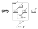
以下、本発明の実施の形態について説明する。図1は、実施形態1に係るレーザアニール装置1の構成例を示す図である。図2は、レーザアニール装置1に含まれる制御装置9の構成例を示す図である。レーザアニール装置1(レーザ照射装置)は、例えば、低温ポリシリコン(LTPS:Low Temperature Poly-Silicon)膜を形成するエキシマレーザアニール(ELA:Excimer laser Anneal)装置である。
図10は、実施形態3(特徴量学習モデル925)に係る特徴量学習モデル925の一例を示す説明図である。実施形態3の制御装置9の制御部91(故障予測部)は、第1真空ポンプ101等の可動部品の振動数、温度、真空到達時間及び積算運転時間から導出した特徴量を、特徴量学習モデル925に入力する。制御装置9の制御部91は、振動数、温度、真空到達時間及び積算運転時間を例えば主成分分析又は次元圧縮することにより、特徴量を導出する。
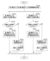
図12、図13、図14、図15及び図16は、その他の実施形態(半導体装置の製造方法)に係る半導体装置の製造方法を示す工程断面図である。その他の実施の形態として、上記実施の形態に係るレーザアニール装置1を用いた半導体装置の製造方法について説明する。以下の半導体装置の製造方法のうち、非晶質の半導体膜を結晶化させる工程において、実施の形態1から4に係るレーザアニール装置1を用いたアニール処理を実施している。
11 アニール光学系
2 レーザ光源
21 第1レーザ光源
22 第2レーザ光源
31 第1アッテネータ
32 第2アッテネータ
41 第1偏光比制御ユニット
42 第2偏光比制御ユニット
5 合成光学系
6 ビーム整形光学系
61 落射ミラー
65 プロジェクションレンズ
7 レーザ照射室
71 ステージ
72 ベース
8 基板
9 制御装置
91 制御部(故障予測部)
92 記憶部
920 記録媒体
P プログラム(プログラム製品)
921 真空ポンプ用学習モデル
922 コールドヘッド用学習モデル
923 Heコンプレッサー用学習モデル
924 ダイアフラムポンプ用学習モデル
925 特徴量学習モデル
93 通信部
94 入出力I/F
941 表示装置
101 第1真空ポンプ
102 第2真空ポンプ
103 コールドヘッド
104 Heコンプレッサー
105 ダイアフラムポンプ
111 温度センサー
112 振動センサー
113 圧力センサー
81 ガラス基板
82 ゲート電極
83 ゲート絶縁膜
84 アモルファスシリコン膜
85 ポリシリコン膜
86 層間絶縁膜
87a ソース電極
87b ドレイン電極
Claims (8)
- レーザ光源を備えるレーザ照射装置であって、
前記レーザ光源による基板の加工を行うにあたり用いられる可動部品の故障予測を行う故障予測部を備え、
前記故障予測部は、
前記可動部品を可動した際の物理量を取得し、
取得した物理量に基づき、前記可動部品の故障時期を導出し、
前記可動部品は、前記レーザ光源のチャンバ内に封入されたガスを吸入する真空ポンプであり、
前記故障予測部は、
前記真空ポンプがガスの吸入を開始してから前記チャンバ内が真空状態となるまでの真空到達時間を取得し、
取得した物理量及び真空到達時間に基づき、前記真空ポンプの故障時期を導出する
レーザ照射装置。 - 前記可動部品には、前記可動部品を可動した際の物理量を検出する検出部が設けられており、
前記検出部は、温度センサー及び振動センサーの少なくともいずれか1つ含み、
前記故障予測部は、前記検出部から、前記可動部品を可動した際の物理量を取得する
請求項1に記載のレーザ照射装置。 - 前記故障予測部は、
前記可動部品を可動した際の物理量を入力した場合に該可動部品の故障までの時間を出力する学習モデルに、取得した物理量を入力することによって、前記可動部品の故障時期を導出する
請求項1又は請求項2に記載のレーザ照射装置。 - 前記故障予測部は、
前記可動部品の積算可動時間を取得し、
取得した積算可動時間及び物理量に基づき、前記可動部品の故障時期を導出する
請求項1から請求項3のいずれか1項に記載のレーザ照射装置。 - 前記レーザ照射装置は、複数の前記レーザ光源、及び複数の前記レーザ光源それぞれに対応する複数の前記真空ポンプを備え、
前記故障予測部は、
複数の前記真空ポンプそれぞれの物理量及び真空到達時間を取得し、
取得した物理量及び真空到達時間それぞれに基づき、複数の前記真空ポンプそれぞれの故障時期を導出する
請求項1から請求項4のいずれか1項に記載のレーザ照射装置。 - 前記可動部品は、ダイアフラムポンプ、ヘリウムコンプレッサー及びコールドヘッドの少なくともいずれか1つ含む
請求項1から請求項5のいずれか1項に記載のレーザ照射装置。 - レーザ照射装置に備えられたレーザ光源による基板の加工を行うにあたり用いられる可動部品の故障予測を行うコンピュータに、
(A)前記可動部品を可動した際の物理量を取得し、
(B)取得した物理量に基づき、前記可動部品の故障時期を導出し、
前記可動部品は、前記レーザ光源のチャンバ内に封入されたガスを吸入する真空ポンプであり、
前記真空ポンプがガスの吸入を開始してから前記チャンバ内が真空状態となるまでの真空到達時間を取得し、
取得した物理量及び真空到達時間に基づき、前記真空ポンプの故障時期を導出する
処理を実行させる情報処理方法。 - レーザ照射装置に備えられたレーザ光源による基板の加工を行うにあたり用いられる可動部品の故障予測を行うコンピュータに、
(A)前記可動部品を可動した際の物理量を取得し、
(B)取得した物理量に基づき、前記可動部品の故障時期を導出し、
前記可動部品は、前記レーザ光源のチャンバ内に封入されたガスを吸入する真空ポンプであり、
前記真空ポンプがガスの吸入を開始してから前記チャンバ内が真空状態となるまでの真空到達時間を取得し、
取得した物理量及び真空到達時間に基づき、前記真空ポンプの故障時期を導出する
処理を実行させるプログラム。
Priority Applications (5)
| Application Number | Priority Date | Filing Date | Title |
|---|---|---|---|
| JP2021109202A JP7637579B2 (ja) | 2021-06-30 | 2021-06-30 | レーザ照射装置、情報処理方法、及びプログラム |
| US17/749,445 US12479050B2 (en) | 2021-06-30 | 2022-05-20 | Laser irradiation apparatus, information processing method, and recording medium recording program to be readable |
| TW111120617A TW202304089A (zh) | 2021-06-30 | 2022-06-02 | 雷射照射裝置、資訊處理方法和可讀取地記錄有程式的記錄介質 |
| CN202210697407.9A CN115548837A (zh) | 2021-06-30 | 2022-06-20 | 激光照射装置、信息处理方法和可读取地记录有程序的记录介质 |
| JP2025006423A JP2025061413A (ja) | 2021-06-30 | 2025-01-16 | レーザ照射装置、情報処理方法、及びプログラム |
Applications Claiming Priority (1)
| Application Number | Priority Date | Filing Date | Title |
|---|---|---|---|
| JP2021109202A JP7637579B2 (ja) | 2021-06-30 | 2021-06-30 | レーザ照射装置、情報処理方法、及びプログラム |
Related Child Applications (1)
| Application Number | Title | Priority Date | Filing Date |
|---|---|---|---|
| JP2025006423A Division JP2025061413A (ja) | 2021-06-30 | 2025-01-16 | レーザ照射装置、情報処理方法、及びプログラム |
Publications (2)
| Publication Number | Publication Date |
|---|---|
| JP2023006547A JP2023006547A (ja) | 2023-01-18 |
| JP7637579B2 true JP7637579B2 (ja) | 2025-02-28 |
Family
ID=84723751
Family Applications (2)
| Application Number | Title | Priority Date | Filing Date |
|---|---|---|---|
| JP2021109202A Active JP7637579B2 (ja) | 2021-06-30 | 2021-06-30 | レーザ照射装置、情報処理方法、及びプログラム |
| JP2025006423A Pending JP2025061413A (ja) | 2021-06-30 | 2025-01-16 | レーザ照射装置、情報処理方法、及びプログラム |
Family Applications After (1)
| Application Number | Title | Priority Date | Filing Date |
|---|---|---|---|
| JP2025006423A Pending JP2025061413A (ja) | 2021-06-30 | 2025-01-16 | レーザ照射装置、情報処理方法、及びプログラム |
Country Status (4)
| Country | Link |
|---|---|
| US (1) | US12479050B2 (ja) |
| JP (2) | JP7637579B2 (ja) |
| CN (1) | CN115548837A (ja) |
| TW (1) | TW202304089A (ja) |
Families Citing this family (3)
| Publication number | Priority date | Publication date | Assignee | Title |
|---|---|---|---|---|
| JP7637579B2 (ja) * | 2021-06-30 | 2025-02-28 | Jswアクティナシステム株式会社 | レーザ照射装置、情報処理方法、及びプログラム |
| US12306595B1 (en) * | 2023-12-26 | 2025-05-20 | Dongguan Pepper Gray Technology Co., Ltd. | Laser packaging system and intelligent heat dissipation method thereof |
| CN117458261B (zh) * | 2023-12-26 | 2024-04-16 | 东莞市湃泊科技有限公司 | 激光器封装系统及其智能散热方法 |
Citations (3)
| Publication number | Priority date | Publication date | Assignee | Title |
|---|---|---|---|---|
| JP2008300351A (ja) | 2007-05-16 | 2008-12-11 | Xtreme Technologies Gmbh | プラズマベースのeuv放射線源用のガスカーテンを生成する装置 |
| US20120209569A1 (en) | 2009-06-26 | 2012-08-16 | Adixen Vacuum Products | Method for predicting a failure in the rotation of the rotor of a vacuum pump and associated pumping device |
| US20150292082A1 (en) | 2014-04-15 | 2015-10-15 | Hitachi Kokusai Electric Inc. | Substrate processing apparatus, non-transitory computer-readable recording medium thereof and semiconductor manufacturing method by employing thereof |
Family Cites Families (18)
| Publication number | Priority date | Publication date | Assignee | Title |
|---|---|---|---|---|
| JPH05190956A (ja) | 1992-01-08 | 1993-07-30 | Toshiba Corp | ガスレ−ザ装置 |
| US5261793A (en) * | 1992-08-05 | 1993-11-16 | The United States Of America As Represented By The Secretary Of The Department Of Health And Human Services | Miniature mechanical vacuum pump |
| JPH0666280A (ja) | 1992-08-20 | 1994-03-08 | Mitsubishi Electric Corp | 真空装置 |
| JP3901758B2 (ja) * | 1994-11-29 | 2007-04-04 | 株式会社半導体エネルギー研究所 | 液晶表示装置の作製方法 |
| US6008101A (en) * | 1994-11-29 | 1999-12-28 | Semiconductor Energy Laboratory Co., Ltd. | Laser processing method of semiconductor device |
| JPH10135196A (ja) * | 1996-10-30 | 1998-05-22 | Matsushita Electric Ind Co Ltd | 真空薄膜堆積装置 |
| JPH11199207A (ja) * | 1997-12-29 | 1999-07-27 | Agency Of Ind Science & Technol | オゾンビーム発生方法及び装置 |
| JP3692106B2 (ja) * | 2002-09-27 | 2005-09-07 | 株式会社東芝 | 製造装置及び回転機の寿命予測方法 |
| EP1836576B1 (en) * | 2004-12-17 | 2012-02-01 | Korea Research Institute of Standards and Science | A precision diagnostic method for the failure protection and predictive maintenance of a vacuum pump and a precision diagnostic system therefor |
| US9104650B2 (en) * | 2005-07-11 | 2015-08-11 | Brooks Automation, Inc. | Intelligent condition monitoring and fault diagnostic system for preventative maintenance |
| US8282360B2 (en) * | 2009-07-07 | 2012-10-09 | Aldo Di Leo | Pneumatically operated reciprocating pump |
| JP5141809B2 (ja) | 2011-09-16 | 2013-02-13 | 住友電気工業株式会社 | 半導体レーザ |
| US9675756B2 (en) * | 2011-12-21 | 2017-06-13 | Deka Products Limited Partnership | Apparatus for infusing fluid |
| CA2880659C (en) * | 2012-08-09 | 2018-10-09 | Wgm Technologies Inc. | Swing chamber pump (scp) |
| US11188065B2 (en) * | 2017-09-23 | 2021-11-30 | Nanoprecise Sci Corp. | System and method for automated fault diagnosis and prognosis for rotating equipment |
| JP7134725B2 (ja) | 2018-06-11 | 2022-09-12 | キヤノン株式会社 | 型を用いて基板上の組成物を成形する成形装置、および物品の製造方法 |
| JP7278138B2 (ja) | 2019-04-18 | 2023-05-19 | キヤノン株式会社 | 基板処理装置、物品製造方法、基板処理方法、基板処理システム、管理装置、およびプログラム |
| JP7637579B2 (ja) * | 2021-06-30 | 2025-02-28 | Jswアクティナシステム株式会社 | レーザ照射装置、情報処理方法、及びプログラム |
-
2021
- 2021-06-30 JP JP2021109202A patent/JP7637579B2/ja active Active
-
2022
- 2022-05-20 US US17/749,445 patent/US12479050B2/en active Active
- 2022-06-02 TW TW111120617A patent/TW202304089A/zh unknown
- 2022-06-20 CN CN202210697407.9A patent/CN115548837A/zh active Pending
-
2025
- 2025-01-16 JP JP2025006423A patent/JP2025061413A/ja active Pending
Patent Citations (5)
| Publication number | Priority date | Publication date | Assignee | Title |
|---|---|---|---|---|
| JP2008300351A (ja) | 2007-05-16 | 2008-12-11 | Xtreme Technologies Gmbh | プラズマベースのeuv放射線源用のガスカーテンを生成する装置 |
| US20120209569A1 (en) | 2009-06-26 | 2012-08-16 | Adixen Vacuum Products | Method for predicting a failure in the rotation of the rotor of a vacuum pump and associated pumping device |
| JP2012530875A (ja) | 2009-06-26 | 2012-12-06 | アデイクセン・バキユーム・プロダクト | 真空ポンプのロータの回転の故障を予測する方法および関連ポンプ装置 |
| US20150292082A1 (en) | 2014-04-15 | 2015-10-15 | Hitachi Kokusai Electric Inc. | Substrate processing apparatus, non-transitory computer-readable recording medium thereof and semiconductor manufacturing method by employing thereof |
| JP2015209561A (ja) | 2014-04-25 | 2015-11-24 | 株式会社日立国際電気 | 基板処理装置、半導体装置の製造方法、プログラムおよび記録媒体 |
Also Published As
| Publication number | Publication date |
|---|---|
| US20230001518A1 (en) | 2023-01-05 |
| JP2025061413A (ja) | 2025-04-10 |
| US12479050B2 (en) | 2025-11-25 |
| CN115548837A (zh) | 2022-12-30 |
| JP2023006547A (ja) | 2023-01-18 |
| TW202304089A (zh) | 2023-01-16 |
Similar Documents
| Publication | Publication Date | Title |
|---|---|---|
| JP2025061413A (ja) | レーザ照射装置、情報処理方法、及びプログラム | |
| CN107199397B (zh) | 机器学习装置、激光加工系统以及机器学习方法 | |
| CN109420859B (zh) | 机器学习装置、机器学习系统以及机器学习方法 | |
| JP7428667B2 (ja) | 機械学習方法、消耗品管理装置、及びコンピュータ可読媒体 | |
| TWI525407B (zh) | 用於自主學習和自主改進半導體製造工具之方法和系統 | |
| TWI524189B (zh) | 用以偵測工具性能劣化及不匹配之方法及系統以及相關電腦程式產品及裝置 | |
| US20190061062A1 (en) | Machine learning device, machine learning system, and machine learning method | |
| JP7637595B2 (ja) | レーザ照射装置、情報処理方法、プログラム、及び学習モデルの生成方法 | |
| US20160126457A1 (en) | Laser crystallization system, laser crystallization method, and method of fabricating display device | |
| US12372815B2 (en) | Laser irradiation apparatus, laser irradiation method, and recording medium recording program to be readable | |
| JPH0423373A (ja) | レーザ制御装置 | |
| CN114556531B (zh) | 激光处理装置及激光监测方法 | |
| TW202244633A (zh) | 用於半導體微影中之光源模組的維護 | |
| US20230006408A1 (en) | Laser Irradiation Apparatus, Laser Irradiation Method, and Recording Medium Recording Program to be Readable | |
| JP2023027639A (ja) | レーザ照射装置、情報処理方法、プログラム、及び学習モデルの生成方法 | |
| CN118176078A (zh) | 激光剥离装置、信息处理方法及程序 | |
| JP4880548B2 (ja) | シリコン半導体薄膜の結晶性評価装置及び方法 | |
| CN107275185A (zh) | 激光退火装置及其退火工艺 | |
| US20240112911A1 (en) | Laser crystallization apparatus and laser crystallization method | |
| WO2024261841A1 (ja) | 制御装置、レーザ加工システム、およびレーザ加工方法 | |
| JP4323550B2 (ja) | レーザ装置 | |
| JP2007123639A (ja) | 分子線エピタキシャル装置の制御装置、分子線エピタキシャル装置、分子線エピタキシャル装置の制御方法、分子線エピタキシャル装置制御プログラム、およびコンピュータ読み取り可能な記録媒体 |
Legal Events
| Date | Code | Title | Description |
|---|---|---|---|
| A711 | Notification of change in applicant |
Free format text: JAPANESE INTERMEDIATE CODE: A711 Effective date: 20220225 |
|
| A621 | Written request for application examination |
Free format text: JAPANESE INTERMEDIATE CODE: A621 Effective date: 20240206 |
|
| A977 | Report on retrieval |
Free format text: JAPANESE INTERMEDIATE CODE: A971007 Effective date: 20241129 |
|
| A131 | Notification of reasons for refusal |
Free format text: JAPANESE INTERMEDIATE CODE: A131 Effective date: 20241203 |
|
| A521 | Request for written amendment filed |
Free format text: JAPANESE INTERMEDIATE CODE: A523 Effective date: 20250116 |
|
| TRDD | Decision of grant or rejection written | ||
| A01 | Written decision to grant a patent or to grant a registration (utility model) |
Free format text: JAPANESE INTERMEDIATE CODE: A01 Effective date: 20250128 |
|
| A61 | First payment of annual fees (during grant procedure) |
Free format text: JAPANESE INTERMEDIATE CODE: A61 Effective date: 20250217 |
|
| R150 | Certificate of patent or registration of utility model |
Ref document number: 7637579 Country of ref document: JP Free format text: JAPANESE INTERMEDIATE CODE: R150 |