JP7624552B2 - 光演算装置、及び、光演算装置の制御方法 - Google Patents
光演算装置、及び、光演算装置の制御方法 Download PDFInfo
- Publication number
- JP7624552B2 JP7624552B2 JP2024501299A JP2024501299A JP7624552B2 JP 7624552 B2 JP7624552 B2 JP 7624552B2 JP 2024501299 A JP2024501299 A JP 2024501299A JP 2024501299 A JP2024501299 A JP 2024501299A JP 7624552 B2 JP7624552 B2 JP 7624552B2
- Authority
- JP
- Japan
- Prior art keywords
- optical
- signal light
- cell
- light
- modulation element
- Prior art date
- Legal status (The legal status is an assumption and is not a legal conclusion. Google has not performed a legal analysis and makes no representation as to the accuracy of the status listed.)
- Active
Links
Images


Classifications
-
- G—PHYSICS
- G06—COMPUTING OR CALCULATING; COUNTING
- G06N—COMPUTING ARRANGEMENTS BASED ON SPECIFIC COMPUTATIONAL MODELS
- G06N3/00—Computing arrangements based on biological models
- G06N3/02—Neural networks
- G06N3/06—Physical realisation, i.e. hardware implementation of neural networks, neurons or parts of neurons
- G06N3/067—Physical realisation, i.e. hardware implementation of neural networks, neurons or parts of neurons using optical means
- G06N3/0675—Physical realisation, i.e. hardware implementation of neural networks, neurons or parts of neurons using optical means using electro-optical, acousto-optical or opto-electronic means
-
- G—PHYSICS
- G02—OPTICS
- G02F—OPTICAL DEVICES OR ARRANGEMENTS FOR THE CONTROL OF LIGHT BY MODIFICATION OF THE OPTICAL PROPERTIES OF THE MEDIA OF THE ELEMENTS INVOLVED THEREIN; NON-LINEAR OPTICS; FREQUENCY-CHANGING OF LIGHT; OPTICAL LOGIC ELEMENTS; OPTICAL ANALOGUE/DIGITAL CONVERTERS
- G02F1/00—Devices or arrangements for the control of the intensity, colour, phase, polarisation or direction of light arriving from an independent light source, e.g. switching, gating or modulating; Non-linear optics
- G02F1/01—Devices or arrangements for the control of the intensity, colour, phase, polarisation or direction of light arriving from an independent light source, e.g. switching, gating or modulating; Non-linear optics for the control of the intensity, phase, polarisation or colour
- G02F1/011—Devices or arrangements for the control of the intensity, colour, phase, polarisation or direction of light arriving from an independent light source, e.g. switching, gating or modulating; Non-linear optics for the control of the intensity, phase, polarisation or colour in optical waveguides, not otherwise provided for in this subclass
-
- G—PHYSICS
- G02—OPTICS
- G02B—OPTICAL ELEMENTS, SYSTEMS OR APPARATUS
- G02B27/00—Optical systems or apparatus not provided for by any of the groups G02B1/00 - G02B26/00, G02B30/00
- G02B27/10—Beam splitting or combining systems
-
- G—PHYSICS
- G06—COMPUTING OR CALCULATING; COUNTING
- G06E—OPTICAL COMPUTING DEVICES
- G06E3/00—Devices not provided for in group G06E1/00, e.g. for processing analogue or hybrid data
-
- G—PHYSICS
- G06—COMPUTING OR CALCULATING; COUNTING
- G06E—OPTICAL COMPUTING DEVICES
- G06E3/00—Devices not provided for in group G06E1/00, e.g. for processing analogue or hybrid data
- G06E3/001—Analogue devices in which mathematical operations are carried out with the aid of optical or electro-optical elements
-
- G—PHYSICS
- G06—COMPUTING OR CALCULATING; COUNTING
- G06G—ANALOGUE COMPUTERS
- G06G7/00—Devices in which the computing operation is performed by varying electric or magnetic quantities
- G06G7/48—Analogue computers for specific processes, systems or devices, e.g. simulators
- G06G7/60—Analogue computers for specific processes, systems or devices, e.g. simulators for living beings, e.g. their nervous systems ; for problems in the medical field
-
- G—PHYSICS
- G06—COMPUTING OR CALCULATING; COUNTING
- G06N—COMPUTING ARRANGEMENTS BASED ON SPECIFIC COMPUTATIONAL MODELS
- G06N3/00—Computing arrangements based on biological models
- G06N3/02—Neural networks
- G06N3/04—Architecture, e.g. interconnection topology
-
- G—PHYSICS
- G06—COMPUTING OR CALCULATING; COUNTING
- G06N—COMPUTING ARRANGEMENTS BASED ON SPECIFIC COMPUTATIONAL MODELS
- G06N3/00—Computing arrangements based on biological models
- G06N3/02—Neural networks
- G06N3/08—Learning methods
-
- G—PHYSICS
- G02—OPTICS
- G02F—OPTICAL DEVICES OR ARRANGEMENTS FOR THE CONTROL OF LIGHT BY MODIFICATION OF THE OPTICAL PROPERTIES OF THE MEDIA OF THE ELEMENTS INVOLVED THEREIN; NON-LINEAR OPTICS; FREQUENCY-CHANGING OF LIGHT; OPTICAL LOGIC ELEMENTS; OPTICAL ANALOGUE/DIGITAL CONVERTERS
- G02F1/00—Devices or arrangements for the control of the intensity, colour, phase, polarisation or direction of light arriving from an independent light source, e.g. switching, gating or modulating; Non-linear optics
- G02F1/01—Devices or arrangements for the control of the intensity, colour, phase, polarisation or direction of light arriving from an independent light source, e.g. switching, gating or modulating; Non-linear optics for the control of the intensity, phase, polarisation or colour
- G02F1/0136—Devices or arrangements for the control of the intensity, colour, phase, polarisation or direction of light arriving from an independent light source, e.g. switching, gating or modulating; Non-linear optics for the control of the intensity, phase, polarisation or colour for the control of polarisation, e.g. state of polarisation [SOP] control, polarisation scrambling, TE-TM mode conversion or separation
-
- G—PHYSICS
- G02—OPTICS
- G02F—OPTICAL DEVICES OR ARRANGEMENTS FOR THE CONTROL OF LIGHT BY MODIFICATION OF THE OPTICAL PROPERTIES OF THE MEDIA OF THE ELEMENTS INVOLVED THEREIN; NON-LINEAR OPTICS; FREQUENCY-CHANGING OF LIGHT; OPTICAL LOGIC ELEMENTS; OPTICAL ANALOGUE/DIGITAL CONVERTERS
- G02F3/00—Optical logic elements; Optical bistable devices
- G02F3/02—Optical bistable devices
Landscapes
- Engineering & Computer Science (AREA)
- Physics & Mathematics (AREA)
- Theoretical Computer Science (AREA)
- General Physics & Mathematics (AREA)
- Biomedical Technology (AREA)
- Health & Medical Sciences (AREA)
- Mathematical Physics (AREA)
- General Health & Medical Sciences (AREA)
- Biophysics (AREA)
- Life Sciences & Earth Sciences (AREA)
- Nonlinear Science (AREA)
- Optics & Photonics (AREA)
- Artificial Intelligence (AREA)
- Computational Linguistics (AREA)
- Computing Systems (AREA)
- General Engineering & Computer Science (AREA)
- Evolutionary Computation (AREA)
- Software Systems (AREA)
- Data Mining & Analysis (AREA)
- Molecular Biology (AREA)
- Neurology (AREA)
- Computer Hardware Design (AREA)
- Neurosurgery (AREA)
- Physiology (AREA)
- Optical Modulation, Optical Deflection, Nonlinear Optics, Optical Demodulation, Optical Logic Elements (AREA)
- Investigating Or Analysing Materials By Optical Means (AREA)
Description
本発明の一実施形態に係る光演算装置1の構成について、図1を参照して説明する。図1は、光演算装置1の構成を示すブロック図である。
光演算装置1が備える反射型の光変調素子11aiの構成例について、図3を参照して説明する。図3の(a)は、本具体例に係る光変調素子11aiの平面図である。図3の(b)は、本具体例に係る光変調素子11aiを構成するマイクロセルCの断面図である。
光演算装置1の一変形例(以下、光演算装置1Aと記載する)について、図2を参照して説明する。図2は、光演算装置1Aの構成を示すブロック図である。
光演算装置1Aが備える透過型の光変調素子11biの構成例について、図4を参照して説明する。図4の(a)は、本具体例に係る光変調素子11biの平面図である。図4の(b)は、本具体例に係る光変調素子11biを構成するマイクロセルCの断面図である。
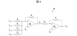
図1に図示した制御部14の一変形例について、図7及び図8を参照して説明する。図7の(a)及び(b)は、制御部14としてマイクロコンピュータの代わりに集積回路を用いる構成のブロック図である。図7の(a)及び(b)においては、光変調素子11aiの一例として光変調素子11a1を示し、イメージセンサ12aiの一例としてイメージセンサ12a1を示している。図8は、図7の(b)に示す加算回路SAの回路図である。
本発明の態様1に係る光演算装置は、少なくとも1個の受光セルを含むイメージセンサと、位相変調量が互いに独立に設定可能な複数のセルを含む光変調素子と、信号光を前記イメージセンサに入射するモニタ用信号光と前記光変調素子に入射する演算用信号光とに分岐する光分岐素子と、前記光変調素子の各セルの位相変調量を、該セルに対応する前記イメージセンサの受光セルにて検出された前記モニタ用信号光の強度に応じて設定する制御部と、を備えている。
本発明は、上述した各実施形態に限定されるものでなく、請求項に示した範囲で種々の変更が可能である。上述した実施形態に含まれる各技術的手段を適宜組み合わせて得られる実施形態についても、本発明の技術的範囲に含まれる。
11 光変調素子群
11a1~11an 光変調素子(反射型)
11b1~11bn 光変調素子(透過型)
12 イメージセンサ群
12a1~12an イメージセンサ
13 光分岐素子群
13a1~13an 光分岐素子
Claims (8)
- 少なくとも1個の受光セルを含むイメージセンサと、
位相変調量が互いに独立に設定可能な複数のセルを含む光変調素子と、
信号光を前記イメージセンサに入射するモニタ用信号光と前記光変調素子に入射する演算用信号光とに分岐する光分岐素子と、
前記光変調素子の各セルの位相変調量を、該セルに対応する前記イメージセンサの受光セルにて検出された前記モニタ用信号光の強度に応じて設定する制御部と、を備えている、
ことを特徴とする光演算装置。 - 前記制御部は、前記光変調素子の各セルの位相変調量Δφ(P)を、Δφ(P)=P×α+βに従って設定する(ここで、Pは、該セルに対応する前記イメージセンサの受光セルにて検出された前記モニタ用信号光の強度であり、α及びβは、定数である)、
ことを特徴とする請求項1に記載の光演算装置。 - 当該光演算装置は、前記光変調素子として、複数の反射型の光変調素子を備え、
前記モニタ用信号光は、前記光分岐素子を透過した信号光であり、
前記演算用信号光は、前記光分岐素子に反射された信号光である、
ことを特徴とする請求項1又は2に記載の光演算装置。 - 前記複数の反射型の光変調素子は、一体化されている、
ことを特徴とする請求項3に記載の光演算装置。 - 当該光演算装置は、前記光変調素子として、複数の透過型の光変調素子を備え、
前記モニタ用信号光は、前記光分岐素子に反射された信号光であり、
前記演算用信号光は、前記光分岐素子を透過した信号光である、
ことを特徴とする請求項1又は2に記載の光演算装置。 - 当該光演算装置は、前記光変調素子、前記イメージセンサ、及び前記光分岐素子の組み合わせを複数段備え、
2段目以降の各段の前記光分岐素子には、該段の前段の光変調素子にて生成された信号光が入力される、
ことを特徴とする請求項1又は2に記載の光演算装置。 - 前記制御部は、前記光変調素子の全てのセルの位相変調量が一定の値に収束した後、正しい演算結果を表す信号光が出力されていることを示す信号を出力する、
ことを特徴とする請求項1又は2に記載の光演算装置。 - 少なくとも1個の受光セルを含むイメージセンサと、位相変調量が互いに独立に設定可能な複数のセルを含む光変調素子と、信号光を前記イメージセンサに入射するモニタ用信号光と前記光変調素子に入射する演算用信号光とに分岐する光分岐素子と、を備えた光演算装置の制御方法であって、
前記光変調素子の各セルの位相変調量を、該セルに対応する前記イメージセンサの受光セルにて検出された前記モニタ用信号光の強度に応じて設定する工程を含む、
ことを特徴とする光演算装置の制御方法。
Applications Claiming Priority (3)
| Application Number | Priority Date | Filing Date | Title |
|---|---|---|---|
| JP2022025020 | 2022-02-21 | ||
| JP2022025020 | 2022-02-21 | ||
| PCT/JP2023/003772 WO2023157694A1 (ja) | 2022-02-21 | 2023-02-06 | 光演算装置、及び、光演算装置の制御方法 |
Publications (3)
| Publication Number | Publication Date |
|---|---|
| JPWO2023157694A1 JPWO2023157694A1 (ja) | 2023-08-24 |
| JPWO2023157694A5 JPWO2023157694A5 (ja) | 2024-09-13 |
| JP7624552B2 true JP7624552B2 (ja) | 2025-01-30 |
Family
ID=87578598
Family Applications (1)
| Application Number | Title | Priority Date | Filing Date |
|---|---|---|---|
| JP2024501299A Active JP7624552B2 (ja) | 2022-02-21 | 2023-02-06 | 光演算装置、及び、光演算装置の制御方法 |
Country Status (5)
| Country | Link |
|---|---|
| US (1) | US20250155735A1 (ja) |
| EP (1) | EP4485121A4 (ja) |
| JP (1) | JP7624552B2 (ja) |
| CN (1) | CN118696286A (ja) |
| WO (1) | WO2023157694A1 (ja) |
Citations (2)
| Publication number | Priority date | Publication date | Assignee | Title |
|---|---|---|---|---|
| JP2007171422A (ja) | 2005-12-20 | 2007-07-05 | Fujikura Ltd | 光学素子及び光学素子を有する光変調器等 |
| JP2009246578A (ja) | 2008-03-31 | 2009-10-22 | Yokogawa Electric Corp | 光送信装置及び光試験装置 |
Family Cites Families (4)
| Publication number | Priority date | Publication date | Assignee | Title |
|---|---|---|---|---|
| US7847225B2 (en) | 2008-05-02 | 2010-12-07 | Hiroshima University | Optical neural network |
| JP5814201B2 (ja) * | 2012-09-10 | 2015-11-17 | 日本電信電話株式会社 | 高速カオス光信号生成光回路 |
| KR102783990B1 (ko) * | 2019-01-24 | 2025-03-24 | 삼성전자주식회사 | 고정 위상 변조기를 구비한 광신경망 장치 |
| US11574178B2 (en) * | 2020-03-11 | 2023-02-07 | Lighton | Method and system for machine learning using optical data |
-
2023
- 2023-02-06 WO PCT/JP2023/003772 patent/WO2023157694A1/ja not_active Ceased
- 2023-02-06 US US18/839,586 patent/US20250155735A1/en active Pending
- 2023-02-06 CN CN202380021570.6A patent/CN118696286A/zh active Pending
- 2023-02-06 JP JP2024501299A patent/JP7624552B2/ja active Active
- 2023-02-06 EP EP23756221.0A patent/EP4485121A4/en active Pending
Patent Citations (2)
| Publication number | Priority date | Publication date | Assignee | Title |
|---|---|---|---|---|
| JP2007171422A (ja) | 2005-12-20 | 2007-07-05 | Fujikura Ltd | 光学素子及び光学素子を有する光変調器等 |
| JP2009246578A (ja) | 2008-03-31 | 2009-10-22 | Yokogawa Electric Corp | 光送信装置及び光試験装置 |
Also Published As
| Publication number | Publication date |
|---|---|
| CN118696286A (zh) | 2024-09-24 |
| US20250155735A1 (en) | 2025-05-15 |
| EP4485121A1 (en) | 2025-01-01 |
| JPWO2023157694A1 (ja) | 2023-08-24 |
| WO2023157694A1 (ja) | 2023-08-24 |
| EP4485121A4 (en) | 2026-03-04 |
Similar Documents
| Publication | Publication Date | Title |
|---|---|---|
| CN111753977A (zh) | 光学神经网络卷积层芯片、卷积计算方法和电子设备 | |
| CN113805641B (zh) | 一种光子神经网络 | |
| CN118414570A (zh) | 光传输路以及光连接器 | |
| CN117157617A (zh) | 用于执行算术运算的装置和方法 | |
| Piao et al. | Programmable photonic time circuits for highly scalable universal unitaries | |
| Dey et al. | All-optical integrated square root of Pauli-Z (SRZ) gates using polarization and phase encoding | |
| JP7624552B2 (ja) | 光演算装置、及び、光演算装置の制御方法 | |
| CN113589435B (zh) | 一种全无源偏振量子态层析方法及芯片 | |
| Ma et al. | Magneto-optics enhances in-memory computing | |
| CN215181644U (zh) | 集成光源和控制非门光量子计算芯片及采用其的教学系统 | |
| CN110275365A (zh) | 一种二进制全光四选一数据选择器 | |
| Raja et al. | Ultra-high-speed all-optical multivalued inverter using nonlinear polarization rotation in semiconductor optical amplifier | |
| US20260016850A1 (en) | Optical computation device | |
| Xu et al. | High-energy-efficiency integrated photonic convolutional neural networks | |
| JPWO2024024414A5 (ja) | ||
| JP7741990B2 (ja) | 光演算装置、光演算装置の学習方法、及び、光演算装置の製造方法 | |
| Liu et al. | Ultra-compact universal linear-optical logic gate based on single rectangle plasmonic slot nanoantenna | |
| Ma et al. | Photonics multiply-accumulation computations system based on residue arithmetic | |
| JP7745655B2 (ja) | 光演算装置及び光演算方法 | |
| Liu et al. | Non-Hermitian optical scattering in cold atoms via four-wave mixing | |
| CN119164501B (zh) | 一种基于强度调制的平衡零差探测装置 | |
| US20240353887A1 (en) | Optical computing device, optical computing method, and manufacturing method for optical computing device | |
| Batabyal et al. | Design of dibit based all optical frequency encoded controlled Fredkin gate using optical switches | |
| CN120235203A (zh) | 光电神经元及光子计算单元 | |
| Yang et al. | Dual-function electro-optical modulation for fully hardware-implemented photonic restricted Boltzmann machine |
Legal Events
| Date | Code | Title | Description |
|---|---|---|---|
| A521 | Request for written amendment filed |
Free format text: JAPANESE INTERMEDIATE CODE: A523 Effective date: 20240702 |
|
| A621 | Written request for application examination |
Free format text: JAPANESE INTERMEDIATE CODE: A621 Effective date: 20240702 |
|
| TRDD | Decision of grant or rejection written | ||
| A01 | Written decision to grant a patent or to grant a registration (utility model) |
Free format text: JAPANESE INTERMEDIATE CODE: A01 Effective date: 20250107 |
|
| A61 | First payment of annual fees (during grant procedure) |
Free format text: JAPANESE INTERMEDIATE CODE: A61 Effective date: 20250120 |
|
| R150 | Certificate of patent or registration of utility model |
Ref document number: 7624552 Country of ref document: JP Free format text: JAPANESE INTERMEDIATE CODE: R150 |