JP7624552B2 - Optical arithmetic device and method for controlling optical arithmetic device - Google Patents
Optical arithmetic device and method for controlling optical arithmetic device Download PDFInfo
- Publication number
- JP7624552B2 JP7624552B2 JP2024501299A JP2024501299A JP7624552B2 JP 7624552 B2 JP7624552 B2 JP 7624552B2 JP 2024501299 A JP2024501299 A JP 2024501299A JP 2024501299 A JP2024501299 A JP 2024501299A JP 7624552 B2 JP7624552 B2 JP 7624552B2
- Authority
- JP
- Japan
- Prior art keywords
- optical
- signal light
- cell
- light
- modulation element
- Prior art date
- Legal status (The legal status is an assumption and is not a legal conclusion. Google has not performed a legal analysis and makes no representation as to the accuracy of the status listed.)
- Active
Links
Images


Classifications
-
- G—PHYSICS
- G06—COMPUTING OR CALCULATING; COUNTING
- G06N—COMPUTING ARRANGEMENTS BASED ON SPECIFIC COMPUTATIONAL MODELS
- G06N3/00—Computing arrangements based on biological models
- G06N3/02—Neural networks
- G06N3/06—Physical realisation, i.e. hardware implementation of neural networks, neurons or parts of neurons
- G06N3/067—Physical realisation, i.e. hardware implementation of neural networks, neurons or parts of neurons using optical means
- G06N3/0675—Physical realisation, i.e. hardware implementation of neural networks, neurons or parts of neurons using optical means using electro-optical, acousto-optical or opto-electronic means
-
- G—PHYSICS
- G02—OPTICS
- G02F—OPTICAL DEVICES OR ARRANGEMENTS FOR THE CONTROL OF LIGHT BY MODIFICATION OF THE OPTICAL PROPERTIES OF THE MEDIA OF THE ELEMENTS INVOLVED THEREIN; NON-LINEAR OPTICS; FREQUENCY-CHANGING OF LIGHT; OPTICAL LOGIC ELEMENTS; OPTICAL ANALOGUE/DIGITAL CONVERTERS
- G02F1/00—Devices or arrangements for the control of the intensity, colour, phase, polarisation or direction of light arriving from an independent light source, e.g. switching, gating or modulating; Non-linear optics
- G02F1/01—Devices or arrangements for the control of the intensity, colour, phase, polarisation or direction of light arriving from an independent light source, e.g. switching, gating or modulating; Non-linear optics for the control of the intensity, phase, polarisation or colour
- G02F1/011—Devices or arrangements for the control of the intensity, colour, phase, polarisation or direction of light arriving from an independent light source, e.g. switching, gating or modulating; Non-linear optics for the control of the intensity, phase, polarisation or colour in optical waveguides, not otherwise provided for in this subclass
-
- G—PHYSICS
- G02—OPTICS
- G02B—OPTICAL ELEMENTS, SYSTEMS OR APPARATUS
- G02B27/00—Optical systems or apparatus not provided for by any of the groups G02B1/00 - G02B26/00, G02B30/00
- G02B27/10—Beam splitting or combining systems
-
- G—PHYSICS
- G06—COMPUTING OR CALCULATING; COUNTING
- G06E—OPTICAL COMPUTING DEVICES
- G06E3/00—Devices not provided for in group G06E1/00, e.g. for processing analogue or hybrid data
-
- G—PHYSICS
- G06—COMPUTING OR CALCULATING; COUNTING
- G06E—OPTICAL COMPUTING DEVICES
- G06E3/00—Devices not provided for in group G06E1/00, e.g. for processing analogue or hybrid data
- G06E3/001—Analogue devices in which mathematical operations are carried out with the aid of optical or electro-optical elements
-
- G—PHYSICS
- G06—COMPUTING OR CALCULATING; COUNTING
- G06G—ANALOGUE COMPUTERS
- G06G7/00—Devices in which the computing operation is performed by varying electric or magnetic quantities
- G06G7/48—Analogue computers for specific processes, systems or devices, e.g. simulators
- G06G7/60—Analogue computers for specific processes, systems or devices, e.g. simulators for living beings, e.g. their nervous systems ; for problems in the medical field
-
- G—PHYSICS
- G06—COMPUTING OR CALCULATING; COUNTING
- G06N—COMPUTING ARRANGEMENTS BASED ON SPECIFIC COMPUTATIONAL MODELS
- G06N3/00—Computing arrangements based on biological models
- G06N3/02—Neural networks
- G06N3/04—Architecture, e.g. interconnection topology
-
- G—PHYSICS
- G06—COMPUTING OR CALCULATING; COUNTING
- G06N—COMPUTING ARRANGEMENTS BASED ON SPECIFIC COMPUTATIONAL MODELS
- G06N3/00—Computing arrangements based on biological models
- G06N3/02—Neural networks
- G06N3/08—Learning methods
-
- G—PHYSICS
- G02—OPTICS
- G02F—OPTICAL DEVICES OR ARRANGEMENTS FOR THE CONTROL OF LIGHT BY MODIFICATION OF THE OPTICAL PROPERTIES OF THE MEDIA OF THE ELEMENTS INVOLVED THEREIN; NON-LINEAR OPTICS; FREQUENCY-CHANGING OF LIGHT; OPTICAL LOGIC ELEMENTS; OPTICAL ANALOGUE/DIGITAL CONVERTERS
- G02F1/00—Devices or arrangements for the control of the intensity, colour, phase, polarisation or direction of light arriving from an independent light source, e.g. switching, gating or modulating; Non-linear optics
- G02F1/01—Devices or arrangements for the control of the intensity, colour, phase, polarisation or direction of light arriving from an independent light source, e.g. switching, gating or modulating; Non-linear optics for the control of the intensity, phase, polarisation or colour
- G02F1/0136—Devices or arrangements for the control of the intensity, colour, phase, polarisation or direction of light arriving from an independent light source, e.g. switching, gating or modulating; Non-linear optics for the control of the intensity, phase, polarisation or colour for the control of polarisation, e.g. state of polarisation [SOP] control, polarisation scrambling, TE-TM mode conversion or separation
-
- G—PHYSICS
- G02—OPTICS
- G02F—OPTICAL DEVICES OR ARRANGEMENTS FOR THE CONTROL OF LIGHT BY MODIFICATION OF THE OPTICAL PROPERTIES OF THE MEDIA OF THE ELEMENTS INVOLVED THEREIN; NON-LINEAR OPTICS; FREQUENCY-CHANGING OF LIGHT; OPTICAL LOGIC ELEMENTS; OPTICAL ANALOGUE/DIGITAL CONVERTERS
- G02F3/00—Optical logic elements; Optical bistable devices
- G02F3/02—Optical bistable devices
Landscapes
- Engineering & Computer Science (AREA)
- Physics & Mathematics (AREA)
- Theoretical Computer Science (AREA)
- General Physics & Mathematics (AREA)
- Biomedical Technology (AREA)
- Health & Medical Sciences (AREA)
- Mathematical Physics (AREA)
- General Health & Medical Sciences (AREA)
- Biophysics (AREA)
- Life Sciences & Earth Sciences (AREA)
- Nonlinear Science (AREA)
- Optics & Photonics (AREA)
- Artificial Intelligence (AREA)
- Computational Linguistics (AREA)
- Computing Systems (AREA)
- General Engineering & Computer Science (AREA)
- Evolutionary Computation (AREA)
- Software Systems (AREA)
- Data Mining & Analysis (AREA)
- Molecular Biology (AREA)
- Neurology (AREA)
- Computer Hardware Design (AREA)
- Neurosurgery (AREA)
- Physiology (AREA)
- Optical Modulation, Optical Deflection, Nonlinear Optics, Optical Demodulation, Optical Logic Elements (AREA)
- Investigating Or Analysing Materials By Optical Means (AREA)
Description
本発明は、光変調素子を備えた光演算装置、及び、そのような光演算装置の制御方法に関する。The present invention relates to an optical arithmetic device having an optical modulation element, and a method for controlling such an optical arithmetic device.
複数のセルを有し、各セルを透過した信号光を相互に干渉させることによって、予め定められた演算を光学的に実行するように設計された光変調素子が知られている。このような光変調素子を用いた光学的な演算には、プロセッサを用いた電気的な演算と比べて高速且つ低消費電力であるという利点がある。また、並べて配置された2つ以上の光変調素子を信号光に順に作用させることによって、複数段光演算を実現することができる。 There is known an optical modulation element that has multiple cells and is designed to optically perform a predetermined calculation by causing the signal light transmitted through each cell to interfere with each other. Optical calculations using such optical modulation elements have the advantage of being faster and consuming less power than electrical calculations using a processor. In addition, multi-stage optical calculations can be realized by sequentially applying the signal light to two or more optical modulation elements arranged side by side.
特許文献1には、入力層、中間層、及び出力層を有する光ニューラルネットワークが開示されている。上述した光変調素子は、例えば、このような光ニューラルネットワークの中間層として利用することが可能である。
しかしながら、光変調素子の各セルにて行われる位相変調は、変調前の信号光の位相φに予め定められた位相Δφを加える線形な位相変調(φ→φ+Δφ)である。したがって、光変調素子にて実現できる光演算は、限定的なものに過ぎなかった。例えば、ニューラルネットワークを構成する各ニューロンでは活性化関数による閾値演算が行われるが、このような閾値演算を光変調素子により実現することは困難であった。However, the phase modulation performed in each cell of the light modulation element is a linear phase modulation (φ→φ+Δφ) in which a predetermined phase Δφ is added to the phase φ of the signal light before modulation. Therefore, the optical calculations that can be realized by light modulation elements are only limited. For example, each neuron that makes up a neural network performs a threshold calculation using an activation function, but it was difficult to realize such a threshold calculation using a light modulation element.
本発明の一態様は、上記の問題に鑑みてなされたものであり、その目的は、光変調素子の各セルにおいて線形な位相変調を行う従来の光演算装置よりも多様な光演算を行うことが可能な光演算装置を実現することにある。One aspect of the present invention has been made in consideration of the above problems, and its purpose is to realize an optical arithmetic device capable of performing more diverse optical arithmetic operations than conventional optical arithmetic devices that perform linear phase modulation in each cell of an optical modulation element.
本発明の一態様に係る光演算装置は、少なくとも1個の受光セルを含むイメージセンサと、位相変調量が互いに独立に設定可能な複数のセルを含む光変調素子と、信号光を前記イメージセンサに入射するモニタ用信号光と前記光変調素子に入射する演算用信号光とに分岐する光分岐素子と、前記光変調素子の各セルの位相変調量を、該セルに対応する前記イメージセンサの受光セルにて検出された前記モニタ用信号光の強度に応じて設定する制御部と、を備えている。An optical computation device according to one embodiment of the present invention comprises an image sensor including at least one light receiving cell, an optical modulation element including a plurality of cells whose phase modulation amounts can be set independently of each other, an optical branching element that branches signal light into a monitor signal light that is incident on the image sensor and an computation signal light that is incident on the optical modulation element, and a control unit that sets the phase modulation amount of each cell of the optical modulation element according to the intensity of the monitor signal light detected by the light receiving cell of the image sensor corresponding to that cell.
本発明の別の態様に係る制御方法は、少なくも1個の受光セルを含むイメージセンサと、位相変調量が互いに独立に設定可能な複数のセルを含む光変調素子と、信号光を前記イメージセンサに入射するモニタ用信号光と前記光変調素子に入射する演算用信号光とに分岐する光分岐素子と、を備えた光演算装置の制御方法であって、前記光変調素子の各セルの位相変調量を、該セルに対応する前記イメージセンサの受光セルにて検出された前記モニタ用信号光の強度に応じて設定する工程を含む。 A control method according to another aspect of the present invention is a control method for an optical arithmetic device comprising an image sensor including at least one light receiving cell, an optical modulation element including a plurality of cells whose phase modulation amounts can be set independently of each other, and an optical branching element that branches signal light into a monitor signal light that is incident on the image sensor and an arithmetic signal light that is incident on the optical modulation element, and includes a step of setting the phase modulation amount of each cell of the optical modulation element in accordance with the intensity of the monitor signal light detected by the light receiving cell of the image sensor corresponding to that cell.
本発明の一態様によれば、光変調素子の各セルにおいて線形な位相変調を行う従来の光演算装置よりも多様な光演算を行うことが可能な光演算装置を実現することができる。According to one aspect of the present invention, it is possible to realize an optical arithmetic device capable of performing more diverse optical arithmetic operations than conventional optical arithmetic devices that perform linear phase modulation in each cell of an optical modulation element.
(光演算装置の構成)
本発明の一実施形態に係る光演算装置1の構成について、図1を参照して説明する。図1は、光演算装置1の構成を示すブロック図である。
(Configuration of the Optical Computing Device)
The configuration of an optical
光演算装置1は、図1に示すように、光変調素子群11と、イメージセンサ群12と、光分岐素子群13と、制御部14と、を備えている。As shown in FIG. 1, the
光変調素子群11は、少なくとも1つの反射型の光変調素子11a1~11an(nは1以上の任意の自然数)の集合である。本実施形態においては、多段の光演算を実現するべく、光変調素子群11として、3つの光変調素子11a1~11a3の集合を用いている。反射型の光変調素子11ai(iは1以上n以下の各自然数)は、位相変調量が互いに独立に設定可能な複数のセルにより構成された板状素子であり、位相変調されながら各セルにて反射された信号光を干渉させることによって、光演算を行う。ここで、光演算を行うとは、信号光の2次元強度分布を、演算前の情報を表す2次元強度分布から、演算後の情報を表す2次元強度分布へと、変換することを指す。反射型の光変調素子11aiの構成例については、参照する図面を代えて後述する。The light
本実施形態において、光変調素子11a1~11anは、各光変調素子11aiの一方の主面(信号光の入出射面)が同一の平面P上に位置するように、並べて配置されている。なお、光変調素子11a1~11anは、一体化されていてもよい。例えば、光変調素子11a1~11anは、単一の基板に埋め込まれていてもよいし、単一の光変調素子のn個の領域を、光変調素子11a1~11anとして用いてもよい。或いは、乾燥ゲルなど、信号光を透過する構造体に中に形成されたn個の光回折層を、光変調素子11a1~11anとして用いてもよい。In this embodiment, the light modulation elements 11a1 to 11an are arranged side by side such that one of the main surfaces (signal light input/output surface) of each light modulation element 11ai is located on the same plane P. The light modulation elements 11a1 to 11an may be integrated. For example, the light modulation elements 11a1 to 11an may be embedded in a single substrate, or n regions of a single light modulation element may be used as the light modulation elements 11a1 to 11an. Alternatively, n light diffraction layers formed in a structure that transmits signal light, such as a dry gel, may be used as the light modulation elements 11a1 to 11an.
イメージセンサ群12は、光変調素子11a1~11anと同数のイメージセンサ12a1~12anの集合である。図1においては、イメージセンサ群12の一例として、3つのイメージセンサ12a1~12a3の集合を図示している。各イメージセンサ12aiは、少なくとも1個の受光セルを含む板状素子であり、信号光の2次元強度分布を検出する。本実施形態においては、光変調素子11aiの各セルとイメージセンサ12aiの各受光セルとが1対1対応している。例えば、光変調素子11aiがマトリックス状に配置された200×200個のセルにより構成される場合、イメージセンサ12aiもマトリックス状に配置された200×200個の受光セルにより構成される。このため、光変調素子11aiの各セルに入射する信号光の強度が、そのセルに対応するイメージセンサ12aiの受光セルによって検出されることになる。なお、イメージセンサ12a1~12anの具体例としては、例えば、CCD(Charge Coupled Device)カメラ及びCMOS(Complementary Metal Oxide Semiconductor)カメラが挙げられる。
The
本実施形態において、イメージセンサ12a1~12anは、各イメージセンサ12aiの一方の主面(信号光の入射面)が同一の平面Q上に位置するように、並べて配置されている。ここで、平面Qは、上述した平面Pと平行な平面である。なお、イメージセンサ12a1~12anは、一体化されていてもよい。例えば、イメージセンサ12a1~12anは、単一の基板に埋め込まれていてもよいし、単一のイメージセンサのn個の領域を、イメージセンサ12a1~12anとして用いてもよい。In this embodiment, the image sensors 12a1-12an are arranged side by side such that one of the main surfaces (the incident surface of the signal light) of each image sensor 12ai is located on the same plane Q. Here, the plane Q is a plane parallel to the above-mentioned plane P. The image sensors 12a1-12an may be integrated. For example, the image sensors 12a1-12an may be embedded in a single substrate, or n regions of a single image sensor may be used as the image sensors 12a1-12an.
光分岐素子群13は、光変調素子11a1~11anと同数の光分岐素子13a1~13anの集合である。図1においては、光分岐素子群13の一例として、3つの光分岐素子13a1~13a3の集合を図示している。各光分岐素子13aiは、信号光をモニタ用信号光と演算用信号光とに分岐する。各光分岐素子13aiは、ハーフミラーであってもよいし、ビームスプリッタであってもよい。
The optical
本実施形態において、光分岐素子13a1~13anは、各光分岐素子13aiの反射面が同一の平面R上に位置するように、並べて配置されている。ここで、平面Rは、上述した平面P及び平面Qの間に位置する、上述した平面P及び平面Qと平行な平面である。In this embodiment, the optical branching elements 13a1 to 13an are arranged side by side such that the reflecting surfaces of the optical branching elements 13ai are located on the same plane R. Here, the plane R is a plane that is located between the above-mentioned planes P and Q and is parallel to the above-mentioned planes P and Q.
制御部14は、各光変調素子11aiの各セルの位相変調量を、そのセルに対応するイメージセンサ12aiの各受光セルにて検出された信号光の強度に応じて制御するための構成である。本実施形態においては、制御部14として、コンピュータの一態様であるマイクロコンピュータを用いる。ただし、本発明の一態様においては、制御部14として、コンピュータの別の態様であるパーソナルコンピュータを用いることもできるし、集積回路を用いることもできる。また、制御部14として集積回路を用いる場合、当該集積回路は、その論理回路を書き換え可能なもの(例えばFPGA(Field-Prоgrammable Gate Array))であってもよいし、書き換え不可能なものであってもよい。書き換え不可能な集積回路は、抵抗やアンプなどで構成された電子回路の集合体、すなわち集積回路である。このような集積回路により構成された制御部14については、図7及び図8を参照して後述する。The
光演算装置1に入力された信号光L0は、光分岐素子13a1によって、モニタ用信号光L0
mと演算用信号光L0
cとに分岐される。ここで、モニタ用信号光L0
mは、光分岐素子13a1を透過した信号光であり、演算用信号光L0
cは、光分岐素子13a1によって反射された信号光である。モニタ用信号光L0
mは、イメージセンサ12a1に入射する。一方、演算用信号光L0
cは、光変調素子11a1に入射する。この際、制御部14は、演算用信号光L0
cに作用する光変調素子11a1の各セルの位相変調量を、そのセルに対応するイメージセンサ12a1の受光セルによって検出されたモニタ用信号光L0
mの強度に応じて設定する。
The signal light L0 input to the
光変調素子11a1によって反射された信号光L1は、光分岐素子13a2によって、モニタ用信号光L1 mと演算用信号光L1 cとに分岐される。ここで、モニタ用信号光L1 mは、光分岐素子13a2を透過した信号光であり、演算用信号光L1 cは、光分岐素子13a2によって反射された信号光である。モニタ用信号光L1 mは、イメージセンサ12a2に入射する。一方、演算用信号光L1 cは、光変調素子11a2に入射する。この際、制御部14は、演算用信号光L1 cに作用する光変調素子11a2の各セルの位相変調量を、そのセルに対応するイメージセンサ12a2の受光セルによって検出されたモニタ用信号光L1 mの強度に応じて設定する。 The signal light L1 reflected by the optical modulation element 11a1 is branched by the optical branching element 13a2 into a monitor signal light L1m and a calculation signal light L1c . Here, the monitor signal light L1m is a signal light transmitted through the optical branching element 13a2, and the calculation signal light L1c is a signal light reflected by the optical branching element 13a2. The monitor signal light L1m is incident on the image sensor 12a2. On the other hand , the calculation signal light L1c is incident on the optical modulation element 11a2. At this time, the control unit 14 sets the phase modulation amount of each cell of the optical modulation element 11a2 acting on the calculation signal light L1c according to the intensity of the monitor signal light L1m detected by the light receiving cell of the image sensor 12a2 corresponding to that cell.
光変調素子11a2によって反射された信号光L2は、光分岐素子13a3によって、モニタ用信号光L2
mと演算用信号光L2
cとに分岐される。ここで、モニタ用信号光L2
mは、光分岐素子13a3を透過した信号光であり、演算用信号光L2
cは、光分岐素子13a3によって反射された信号光である。モニタ用信号光L2
mは、イメージセンサ12a3に入射する。一方、演算用信号光L2
cは、光変調素子11a3に入射する。この際、制御部14は、演算用信号光L2
cに作用する光変調素子11a3の各セルの位相変調量を、そのセルに対応するイメージセンサ12a3の受光セルによって検出されたモニタ用信号光L2
mの強度に応じて設定する。
The signal light L2 reflected by the light modulation element 11a2 is branched by the light branching element 13a3 into a monitor signal light L2m and a calculation signal light L2c . Here, the monitor signal light L2m is a signal light transmitted through the light branching element 13a3, and the calculation signal light L2c is a signal light reflected by the light branching element 13a3. The monitor signal light L2m enters the image sensor 12a3. On the other hand , the calculation signal light L2c enters the light modulation element 11a3. At this time, the
光変調素子11a3に反射された信号光L3は、光演算装置1による演算結果を表す信号光として、外部に出力される。
The signal light L3 reflected by the light modulation element 11a3 is output to the outside as a signal light representing the result of the calculation by the
なお、本実施形態においては、入力情報を表す信号光L0が光演算装置1に入力される構成を採用しているが、本発明は、これに限定されない。例えば、入力情報を表す電気信号と搬送光とが光演算装置1に入力される構成を採用することもできる。この場合、例えば、入力情報を表す電気信号で搬送光を光変調することによって、入力信号を表す信号光L0を生成する光変調素子11a0(図1において点線で図示)を、光変調素子11a1の前段に追加するとよい。
In this embodiment, a configuration is adopted in which the signal light L0 representing the input information is input to the optical
従来の光演算装置が備える光変調素子の各セルの位相変調量は、そのセルに入射する信号光の強度(光強度)Pに依らず一定である。したがって、そのセルに入射する信号光の位相をφ、そのセルにおける位相変調量をΔφとすると、そのセルから出射する信号光の位相φ’は、φ’=φ+Δφ(定数)により与えられる。換言すると、セルに入射する信号光を複素数P×ei×φにより表現する場合、そのセルから出射する信号光は、複素数P×ei×φ×ei×Δθにより表現される。 The phase modulation amount of each cell of the optical modulation element included in the conventional optical arithmetic device is constant regardless of the intensity (optical intensity) P of the signal light incident on the cell. Therefore, if the phase of the signal light incident on the cell is φ and the phase modulation amount in the cell is Δφ, the phase φ' of the signal light emitted from the cell is given by φ' = φ + Δφ (constant). In other words, when the signal light incident on a cell is expressed by the complex number P x e i x φ , the signal light emitted from the cell is expressed by the complex number P x e i x φ x e i x Δθ .
一方、本実施形態に係る光演算装置1が備える光変調素子11aiの各セルの位相変調量は、そのセルに入射する演算用信号光Li-1
cの強度P、すなわち、そのセルに対応するイメージセンサ12aiの受光セルが検出したモニタ用信号光Li-1
mの強度Pに応じて決まる。したがって、そのセルに入射する演算用信号光Li-1
cの位相をφ、そのセルにおける位相変調量をΔφ(P)とすると、そのセルから出射する信号光Liの位相をφ’は、φ’=φ+Δφ(P)により与えられる。換言すると、各セルに入射する演算用信号光Li-1
cを複素数Peiφにより表現する場合、そのセルから出射する信号光Liは、複素数P×ei×φ×ei×Δθ(P)により表現される。このため、本実施形態に係る光演算装置1によれば、光変調素子の各セルにおいて線形な位相変調を行う従来の光演算装置よりも多様な光演算を行うことができる。
On the other hand, the phase modulation amount of each cell of the light modulation element 11ai included in the optical
なお、演算用信号光Li-1 cの強度Pcとモニタ用信号光Li-1 mの強度Pmとは、一致することもあれば、一致しないこともある。ただし、後者の場合であっても、これらの強度の間には比例関係Pc=ρPmが存在するので、演算用信号光Li-1 cの強度Pcに応じた位相変調量の制御を行うことができる。ここで、ρは、光分岐素子13aiの分岐比(透過率及び反射率)などに応じて定まる定数である。 The intensity Pc of the calculation signal light L i-1c and the intensity Pm of the monitor signal light L i-1m may or may not be the same. However, even in the latter case, since there is a proportional relationship Pc = ρPm between these intensities, it is possible to control the phase modulation amount according to the intensity Pc of the calculation signal light L i-1c . Here, ρ is a constant determined according to the branching ratio (transmittance and reflectance) of the optical branching element 13ai.
なお、本実施形態において、制御部14は、光変調素子11aiの各セルの位相変調量Δφ(P)を、Δφ(P)=P×α+βに従って設定する。ここで、α及びβは、光変調素子11aiのセル毎に定まる定数である。ただし、本発明は、これに限定されない。すなわち、各セルの位相変調量Δφ(P)と、そのセルに対応するイメージセンサ12aiの受光セルが検出したモニタ用信号光Li-1
mの強度Pとの関係は任意である。例えば、制御部14は、光変調素子11aiの各セルの位相変調量Δφ(P)を、P<P0であればΔφ(P)=0となり、P≧P0であればΔφ(P)=γとなるように設定してもよい。ここで、γは、光変調素子11aiのセル毎に定まる定数である。
In this embodiment, the
なお、光変調素子11aiの各セルの位相変調量の定数部分の設定は、例えば、機械学習を用いて実現することができる。この機械学習において用いられるモデルとしては、例えば、光変調素子11a1に入力される信号光L0の2次元強度分布を入力とし、光変調素子11anから出力される信号光Lnの2次元強度分布を出力とするモデルであって、各セルにおける位相変調量の定数部分(上述した例では、α、β、及びγ)をパラメータとして含むモデルを用いることができる。ここで、光変調素子11a1に入力される信号光L0の2次元強度分布とは、例えば、光変調素子11a1を構成する各セルに入力される信号光の強度の集合のことを指す。また、光変調素子11anから出力される信号光Lnの2次元強度分布とは、例えば、光変調素子11anの後段に配置された2次元イメージセンサを構成する各セルに入力される信号光の強度の集合のことを指す。 The setting of the constant part of the phase modulation amount of each cell of the light modulation element 11ai can be realized, for example, by using machine learning. As a model used in this machine learning, for example, a model in which the two-dimensional intensity distribution of the signal light L 0 input to the light modulation element 11a1 is input and the two-dimensional intensity distribution of the signal light L n output from the light modulation element 11an is output, and a model including the constant part of the phase modulation amount in each cell (α, β, and γ in the above example) as a parameter can be used. Here, the two-dimensional intensity distribution of the signal light L 0 input to the light modulation element 11a1 refers to, for example, a set of the intensities of the signal light input to each cell constituting the light modulation element 11a1. In addition, the two-dimensional intensity distribution of the signal light L n output from the light modulation element 11an refers to, for example, a set of the intensities of the signal light input to each cell constituting a two-dimensional image sensor arranged in the rear stage of the light modulation element 11an.
なお、各イメージセンサ12aiによるモニタ用信号光Li-1
mの検出、制御部14による各光変調素子11aiの制御、及び、各光変調素子11aiによる演算用信号光Li-1
cに対する光演算は、それぞれ、時間を要する処理である。したがって、各光変調素子11aiの全てのセルの位相変調量が一定の値に収束し、光演算装置1から期待される信号光Lnが出力されるようになるまでには、時間が掛かる。この点を考慮すると、制御部14は、各光変調素子11aiの全てのセルの位相変調量が一定の値に収束した後、正しい演算結果を表す信号光Lnが出力されていることを示す信号(光信号であってもよいし、電気信号であってもよい)を出力することが好ましい。これにより、この信号の出力先において、各光変調素子11aiの全てのセルの位相変調量が一定の値に収束する前に光演算装置1から出力され得る、正しくない演算結果を表す信号光Lnが参照されるリスクを低減することができる。なお、この信号の出力先としては、例えば、信号光Lnが表す情報を利用する装置の制御部(その装置に接続されたコンピュータであってもよいし、その装置に内蔵されたマイコン又は集積回路であってもよい)などが挙げられる。
In addition, the detection of the monitor signal light L i-1 m by each image sensor 12ai, the control of each light modulation element 11ai by the
また、本実施形態においては、光変調素子11aiの各セルとイメージセンサ12aiの各受光セルとが1対1対応する構成を採用しているが、本発明はこれに限定されない。例えば、光変調素子11aiの各セルとイメージセンサ12aiの各受光セルとが1対K対応する構成を採用してもよい(Kは2以上の自然数)。この場合、制御部14は、光変調素子11aiの1個のセルの位相変調量Δφ(P)を、そのセルに対応するイメージセンサ12aiのK個の受光セルにて検出されたモニタ用信号光Li-1
mの強度Pに応じて設定することになる。K=4の場合について、図7の(b)を参照して後述する。或いは、光変調素子11aiの各セルとイメージセンサ12aiの各受光セルとがL対1対応する構成を採用してもよい(Lは2以上の自然数)。この場合、制御部14は、光変調素子11aiのL個のセルの位相変調量Δφ(P)を、それらのセルに対応するイメージセンサ12aiの1個の受光セルにて検出されたモニタ用信号光Li-1
mの強度Pに応じて設定することになる。なお、Lは、光変調素子11aiを構成するセルの総数であってもよい。この場合、光変調素子11aiの全てのセルの位相変調量Δφ(P)が、それらのセルに対応するイメージセンサ12aiの1個の受光セルにて検出されたモニタ用信号光Li-1
mの強度Pに応じて設定することになる。
In addition, in this embodiment, a configuration in which each cell of the light modulation element 11ai corresponds to each light receiving cell of the image sensor 12ai on a one-to-one basis is adopted, but the present invention is not limited to this. For example, a configuration in which each cell of the light modulation element 11ai corresponds to each light receiving cell of the image sensor 12ai on a one-to-K basis (K is a natural number of 2 or more). In this case, the
また、乾燥ゲル中に形成されたn個の光回折層を光変調素子11a1~11anとして用いる場合、脱水収縮を行うことにより相似形を保ったまま収縮するゲル、例えば、Implosion Fabrication法において用いられるゲルを用いることが好ましい。これにより、n個の光回折層を形成した膨潤ゲルを乾燥させることによって、光変調素子11a1~11anが精度良く配置された光変調素子群11を容易に製造することができる。In addition, when using n optical diffraction layers formed in a dry gel as the optical modulation elements 11a1 to 11an, it is preferable to use a gel that shrinks while maintaining a similar shape by dehydration shrinkage, for example, a gel used in the Implosion Fabrication method. This makes it possible to easily manufacture an optical
(反射型の光変調素子の構成例)
光演算装置1が備える反射型の光変調素子11aiの構成例について、図3を参照して説明する。図3の(a)は、本具体例に係る光変調素子11aiの平面図である。図3の(b)は、本具体例に係る光変調素子11aiを構成するマイクロセルCの断面図である。
(Example of the configuration of a reflective light modulation element)
A configuration example of the reflective light modulation element 11ai included in the
光変調素子11aiは、図3の(a)に示すように、位相変調量が互いに独立に設定された複数のマイクロセルCにより構成されている。光変調素子11aiに演算用信号光Li-1 cが入射すると、位相変調されながら各マイクロセルCで反射された演算用信号光Li-1 cが相互に干渉することによって、演算結果を表す信号光Liが形成される。 3A, the optical modulation element 11ai is composed of a plurality of microcells C in which the phase modulation amount is set independently of each other. When the calculation signal light L i-1 c is incident on the optical modulation element 11ai, the calculation signal light L i-1 c reflected by each microcell C while being phase modulated interferes with each other to form a signal light L i representing the calculation result.
なお、本明細書において、「マイクロセル」とは、例えば、セルサイズが10μm未満のセルのことを指す。また、「セルサイズ」とは、セルの面積の平方根のことを指す。例えば、マイクロセルCの平面視形状が正方形である場合、マイクロセルCのセルサイズとは、マイクロセルCの一辺の長さである。マイクロセルCのセルサイズの下限は、例えば、1nmである。In this specification, a "microcell" refers to a cell having a cell size of less than 10 μm, for example. Also, "cell size" refers to the square root of the cell area. For example, when the planar shape of a microcell C is a square, the cell size of the microcell C is the length of one side of the microcell C. The lower limit of the cell size of the microcell C is, for example, 1 nm.
図3の(a)に例示した光変調素子11aiは、マトリックス状に配置された200×200個のマイクロセルCにより構成されている。各マイクロセルCの平面視形状は、500nm×500nmの正方形であり、光変調素子11aiの平面視形状は、100μm×100μmの正方形である。The light modulation element 11ai shown in FIG. 3A is composed of 200 x 200 microcells C arranged in a matrix. The planar shape of each microcell C is a square of 500 nm x 500 nm, and the planar shape of the light modulation element 11ai is a square of 100 μm x 100 μm.
光変調素子11aiを構成する各マイクロセルCは、例えば図3の(b)に示すように、偏光板C11と、反射板C12と、第1電極C13と、磁化自由層C14と、絶縁層C15と、磁化固定層C16と、第2電極C17と、により構成することができる。Each microcell C constituting the light modulation element 11ai can be composed of a polarizing plate C11, a reflecting plate C12, a first electrode C13, a magnetization free layer C14, an insulating layer C15, a magnetization fixed layer C16, and a second electrode C17, for example, as shown in (b) of Figure 3.
偏光板C11及び反射板C12は、互いに対向するように配置されている。第1電極C13、磁化自由層C14、絶縁層C15、磁化固定層C16、及び第2電極C17は、この順に積層され、偏光板C11と反射板C12との間に挟みこまれている。ここで、第1電極C13、磁化自由層C14、絶縁層C15、磁化固定層C16、及び第2電極C17の積層方向は、偏光板C11及び反射板C12の積層方向と直交する。このため、磁化自由層C14の第1の側面が偏光板C11の一方の主面と面接触し、第1の側面に対向する磁化自由層C14の第2の側面が反射板C12の一方の主面と面接触する。演算用信号光Li-1 cは、(1)偏光板C11を介して磁化自由層C14の内部に入射し、(2)反射板C12により反射され、(3)偏光板C11を介して磁化自由層C14の外部に出射する。 The polarizing plate C11 and the reflecting plate C12 are arranged to face each other. The first electrode C13, the magnetization free layer C14, the insulating layer C15, the magnetization fixed layer C16, and the second electrode C17 are stacked in this order and sandwiched between the polarizing plate C11 and the reflecting plate C12. Here, the stacking direction of the first electrode C13, the magnetization free layer C14, the insulating layer C15, the magnetization fixed layer C16, and the second electrode C17 is perpendicular to the stacking direction of the polarizing plate C11 and the reflecting plate C12. Therefore, the first side surface of the magnetization free layer C14 is in surface contact with one of the main surfaces of the polarizing plate C11, and the second side surface of the magnetization free layer C14 facing the first side surface is in surface contact with one of the main surfaces of the reflecting plate C12. The calculation signal light L i-1 c (1) enters the magnetization free layer C14 via the polarizing plate C11, (2) is reflected by the reflecting plate C12, and (3) exits the magnetization free layer C14 via the polarizing plate C11.
磁化自由層C14は、例えば、導電性及び透光性を有する軟磁性材料(例えば、CoFeB)により構成される。また、磁化固定層C16は、例えば、導電性を有する硬磁性材料(例えば、パーマロイ)により構成される。また、偏光板C11としては、偏光方向Pが磁化固定層C16の磁化方向Mと平行な偏光成分を選択的に透過する偏光板が選択される。図3の(b)においては、磁化方向M及び偏光方向Pが、偏光板C11の主面及び磁化固定層C16の主面の両方と平行になる場合を例示している。The magnetization free layer C14 is made of, for example, a soft magnetic material (e.g., CoFeB) that is conductive and translucent. The magnetization fixed layer C16 is made of, for example, a hard magnetic material (e.g., Permalloy) that is conductive. The polarizer C11 is selected to selectively transmit the polarized light component whose polarization direction P is parallel to the magnetization direction M of the magnetization fixed layer C16. Figure 3 (b) illustrates a case where the magnetization direction M and the polarization direction P are parallel to both the main surface of the polarizer C11 and the main surface of the magnetization fixed layer C16.
第1電極C13と第2電極C17との間に電位差を与えると、トンネル効果によりスピン流(スピン偏極した電子の流れ)が絶縁層C15を介して磁化固定層C16から磁化自由層C14に注入され、磁化自由層C14に磁化が生じる。ここで、磁化自由層C14に生じる磁化は、磁化固定層C16の磁化方向Mと平行な磁化、すなわち、偏光板C11を介して磁化自由層C14に入射する演算用信号光Li-1 cの偏光方向Pと平行な磁化である。このため、演算用信号光Li-1 cの位相は、磁化自由層C14を伝搬する過程で横カー効果により遅延する。 When a potential difference is applied between the first electrode C13 and the second electrode C17, a spin current (a flow of spin-polarized electrons) is injected from the magnetization fixed layer C16 through the insulating layer C15 into the magnetization free layer C14 due to the tunnel effect, and magnetization occurs in the magnetization free layer C14. Here, the magnetization generated in the magnetization free layer C14 is magnetization parallel to the magnetization direction M of the magnetization fixed layer C16, that is, magnetization parallel to the polarization direction P of the operation signal light L i-1 c incident on the magnetization free layer C14 through the polarizing plate C11. For this reason, the phase of the operation signal light L i-1 c is delayed by the transverse Kerr effect in the process of propagating through the magnetization free layer C14.
ここで、セルCにおける演算用信号光Li-1 cの位相変化量は、磁化自由層C14に生じる磁化の大きさに応じて決まる。また、磁化自由層C14に生じる磁化の大きさは、磁化自由層C14に注入されるスピン流の大きさに応じて決まる。また、磁化自由層C14に注入されるスピン流の大きさは、第1電極C13と第2電極C17との間に与える電位差に応じて決まる。したがって、第1電極C13と第2電極C17との間に与える電位差を制御することによって、セルCの位相変調を所望の値に設定することができる。 Here, the amount of phase change of the calculation signal light L i-1 c in cell C is determined according to the magnitude of magnetization generated in the magnetization free layer C14. Moreover, the magnitude of magnetization generated in the magnetization free layer C14 is determined according to the magnitude of the spin current injected into the magnetization free layer C14. Moreover, the magnitude of the spin current injected into the magnetization free layer C14 is determined according to the potential difference applied between the first electrode C13 and the second electrode C17. Therefore, by controlling the potential difference applied between the first electrode C13 and the second electrode C17, the phase modulation of cell C can be set to a desired value.
なお、本構成例においては、STT(Spin Transfer Torque)方式のMRAM(Magnetoresistive Random Access Memory)と同様の構成を有するマイクロセルCについて説明したが、これに限定されない。例えば、SOT(Spin Orbit Torque)方式のMRAMと同様の構成を有するマイクロセルCを用いてもよい。なお、このようなマイクロセルCは、例えば、図3の(b)に示した構造から、絶縁層C15、磁化固定層C16、及び第2電極C17を取り去ることにより実現することができる。この場合、例えば、第1電極C13に重金属を含め、第1電極C13にパルス電圧又はパルス電流を与えることにより、磁化自由層C14に効率よくスピン流を注入することができる。In this configuration example, the microcell C having a configuration similar to that of a STT (Spin Transfer Torque) type MRAM (Magnetoresistive Random Access Memory) has been described, but the present invention is not limited thereto. For example, a microcell C having a configuration similar to that of a SOT (Spin Orbit Torque) type MRAM may be used. Such a microcell C can be realized, for example, by removing the insulating layer C15, the magnetization fixed layer C16, and the second electrode C17 from the structure shown in FIG. 3B. In this case, for example, by including a heavy metal in the first electrode C13 and applying a pulse voltage or pulse current to the first electrode C13, a spin current can be efficiently injected into the magnetization free layer C14.
また、セルCは、LCOS(Liquid Crystal On Silicon)のセルと同様に構成されていてもよい。この場合、セルCは、例えば図5に示すように、ガラス基板C21、透明電極C22、液晶層C23、及び反射電極C24により構成される。ガラス基板C21、透明電極C22、液晶層C23、及び反射電極C24は、演算用信号光Li-1 cの入射側からこの順に積層されている。 Furthermore, the cell C may be configured similarly to a LCOS (Liquid Crystal On Silicon) cell. In this case, the cell C is configured, for example, as shown in Fig. 5, of a glass substrate C21, a transparent electrode C22, a liquid crystal layer C23, and a reflective electrode C24. The glass substrate C21, the transparent electrode C22, the liquid crystal layer C23, and the reflective electrode C24 are laminated in this order from the incident side of the calculation signal light L i-1 c .
演算用信号光Li-1 cは、(1)ガラス基板C21及び透明電極C22を透過し、(2)液晶層C23を透過し、(3)反射電極C24により反射され、(4)液晶層C23を透過し、(5)透明電極C22及びガラス基板C21を透過する。液晶層C23は、ガラス基板C21の主面と平行な方向に配向した液晶分子により構成されており、透明電極C22と反射電極C24との間の電位差に応じた屈折率を有する。このため、演算用信号光Li-1 cは、液晶層C23を透過する際に、位相変調を受ける。セルCの位相変調量は、透明電極C22と反射電極C24との間に与える電位差を制御することによって、所望の値に設定することができる。 The calculation signal light L i-1 c (1) passes through the glass substrate C21 and the transparent electrode C22, (2) passes through the liquid crystal layer C23, (3) is reflected by the reflective electrode C24, (4) passes through the liquid crystal layer C23, and (5) passes through the transparent electrode C22 and the glass substrate C21. The liquid crystal layer C23 is composed of liquid crystal molecules oriented in a direction parallel to the main surface of the glass substrate C21, and has a refractive index according to the potential difference between the transparent electrode C22 and the reflective electrode C24. Therefore, the calculation signal light L i-1 c is subjected to phase modulation when passing through the liquid crystal layer C23. The amount of phase modulation of the cell C can be set to a desired value by controlling the potential difference applied between the transparent electrode C22 and the reflective electrode C24.
(光演算装置の変形例)
光演算装置1の一変形例(以下、光演算装置1Aと記載する)について、図2を参照して説明する。図2は、光演算装置1Aの構成を示すブロック図である。
(Modification of the Optical Computing Device)
A modified example of the optical arithmetic device 1 (hereinafter, referred to as optical
光演算装置1Aは、光演算装置1と同様、光変調素子群11と、イメージセンサ群12と、光分岐素子群13と、制御部14と、を備えている。光演算装置1と光演算装置1Aとの相違点は、(1)光変調素子群11が透過型の光変調素子11b1~11bnにより構成されている点と、(2)光変調素子群11に含まれる光変調素子11b1~11bn、及び、光分岐素子群13に含まれる光分岐素子13a1~13anの配置である。Like the optical
透過型の光変調素子11biは、位相変調量が互いに独立に設定可能な複数のセルにより構成されており、位相変調されながら各セルを透過した信号光を干渉させることによって、光演算を行う。透過型の光変調素子11biの構成例については、参照する図面を代えて後述する。The transmissive optical modulation element 11bi is composed of multiple cells whose phase modulation amount can be set independently of each other, and performs optical calculations by interfering with the signal light that is transmitted through each cell while being phase modulated. An example of the configuration of the transmissive optical modulation element 11bi will be described later with reference to a different drawing.
本変形例において、光変調素子11b1~11bnは、各光変調素子11biの主面(信号光の入射面及び出射面)が平面Qと直交するように、直線S上に並べて配置されている。ここで、平面Qは、各イメージセンサ12aiの一方の主面(信号光の入射面)が配置される平面であり、直線Sは、平面Qと平行な直線である。In this modified example, the light modulation elements 11b1 to 11bn are arranged side by side on a straight line S so that the principal surface (the incident surface and the exit surface of the signal light) of each light modulation element 11bi is perpendicular to a plane Q. Here, the plane Q is the plane on which one principal surface (the incident surface of the signal light) of each image sensor 12ai is arranged, and the straight line S is a straight line parallel to the plane Q.
光分岐素子13a1は、光変調素子11b1の前段において、直線S上に配置される。また、光分岐素子13aj(jは2以上n以下の各自然数)は、光変調素子11bj-1の後段かつ光変調素子11bjの前段において、直線S上に配置される。光分岐素子13aiの向きは、光分岐素子13aiの反射面の法線が平面Tに含まれ、かつ、光分岐素子13aiの反射面と直線Sとが45°を成し、かつ、モニタ用信号光Li-1 mがイメージセンサ12aiに向かうように決められている。ここで、平面Tは、直線Sを含み平面Qと直交する平面である。 The optical branching element 13a1 is disposed on the straight line S in front of the optical modulation element 11b1. The optical branching element 13aj (j is a natural number between 2 and n) is disposed on the straight line S in front of the optical modulation element 11bj-1 and in front of the optical modulation element 11bj. The orientation of the optical branching element 13ai is determined such that the normal to the reflecting surface of the optical branching element 13ai is included in the plane T, the reflecting surface of the optical branching element 13ai and the straight line S form an angle of 45°, and the monitor signal light L i-1 m is directed toward the image sensor 12ai. Here, the plane T is a plane that includes the straight line S and is perpendicular to the plane Q.
光演算装置1Aに入力された信号光L0は、光分岐素子13a1によって、モニタ用信号光L0
mと演算用信号光L0
cとに分岐される。ここで、モニタ用信号光L0
mは、光分岐素子13a1によって反射された信号光であり、演算用信号光L0
cは、光分岐素子13a1を透過した信号光である。モニタ用信号光L0
mは、イメージセンサ12a1に入射する。一方、演算用信号光L0
cは、光変調素子11b1に入射する。この際、制御部14は、演算用信号光L0
cに作用する光変調素子11b1の各セルの位相変調量を、そのセルに対応するイメージセンサ12a1の受光セルによって検出されたモニタ用信号光L0
mの強度に応じて設定する。
The signal light L0 input to the
光変調素子11b1を透過した信号光L1は、光分岐素子13a2によって、モニタ用信号光L1 mと演算用信号光L1 cとに分岐される。ここで、モニタ用信号光L1 mは、光分岐素子13a2によって反射された信号光であり、演算用信号光L1 cは、光分岐素子13a2を透過した信号光である。モニタ用信号光L1 mは、イメージセンサ12a2に入射する。一方、演算用信号光L1 cは、光変調素子11b2に入射する。この際、制御部14は、演算用信号光L1 cに作用する光変調素子11b2の各セルの位相変調量を、そのセルに対応するイメージセンサ12a2の受光セルによって検出されたモニタ用信号光L1 mの強度に応じて設定する。 The signal light L1 transmitted through the optical modulation element 11b1 is branched by the optical branching element 13a2 into a monitor signal light L1m and an arithmetic signal light L1c . Here, the monitor signal light L1m is the signal light reflected by the optical branching element 13a2, and the arithmetic signal light L1c is the signal light transmitted through the optical branching element 13a2. The monitor signal light L1m enters the image sensor 12a2. On the other hand, the arithmetic signal light L1c enters the optical modulation element 11b2. At this time, the control unit 14 sets the phase modulation amount of each cell of the optical modulation element 11b2 acting on the arithmetic signal light L1c according to the intensity of the monitor signal light L1m detected by the light receiving cell of the image sensor 12a2 corresponding to that cell.
光変調素子11b2を透過した信号光L2は、光分岐素子13a3によって、モニタ用信号光L2 mと演算用信号光L2 cとに分岐される。ここで、モニタ用信号光L2 mは、光分岐素子13a3によって反射された信号光であり、演算用信号光L2 cは、光分岐素子13a3を透過した信号光である。モニタ用信号光L2 mは、イメージセンサ12a3に入射する。一方、演算用信号光L2 cは、光変調素子11b3に入射する。この際、制御部14は、演算用信号光L2 cに作用する光変調素子11b3の各セルの位相変調量を、そのセルに対応するイメージセンサ12a3の受光セルによって検出されたモニタ用信号光L2 mの強度に応じて設定する。 The signal light L2 transmitted through the optical modulation element 11b2 is branched by the optical branching element 13a3 into a monitor signal light L2m and a calculation signal light L2c . Here, the monitor signal light L2m is the signal light reflected by the optical branching element 13a3, and the calculation signal light L2c is the signal light transmitted through the optical branching element 13a3. The monitor signal light L2m enters the image sensor 12a3. On the other hand, the calculation signal light L2c enters the optical modulation element 11b3. At this time, the control unit 14 sets the phase modulation amount of each cell of the optical modulation element 11b3 acting on the calculation signal light L2c according to the intensity of the monitor signal light L2m detected by the light receiving cell of the image sensor 12a3 corresponding to that cell.
光変調素子11b3を透過した信号光L3は、光演算装置1Aによる演算結果を表す信号光として、外部に出力される。
The signal light L3 transmitted through the light modulation element 11b3 is outputted to the outside as a signal light representing the result of the calculation by the
なお、本実施形態においては、入力情報を表す信号光L0が光演算装置1Aに入力される構成を採用しているが、本発明は、これに限定されない。例えば、入力情報を表す電気信号と搬送光とが光演算装置1Aに入力される構成を採用することもできる。この場合、例えば、入力情報を表す電気信号で搬送光を光変調することによって、入力信号を表す信号光L0を生成する光変調素子11b0(図2において点線で図示)を、光変調素子11b1の前段に追加するとよい。
In this embodiment, a configuration is adopted in which the signal light L0 representing the input information is input to the optical
本変形例に係る光演算装置1Aが備える光変調素子11biの各セルの位相変調量は、そのセルに入射する演算用信号光Li-1
cの強度P、すなわち、そのセルに対応するイメージセンサ12aiの受光セルが検出したモニタ用信号光Li-1
mの強度Pに応じて決まる。したがって、そのセルに入射する演算用信号光Li-1
cの位相をφ、そのセルにおける位相変調量をΔφ(P)とすると、そのセルから出射する信号光Liの位相φ’は、φ’=φ+Δφ(P)により与えられる。換言すると、各セルに入射する演算用信号光Li-1
cを複素数Peiφにより表現する場合、そのセルから出射する信号光Liは、複素数Peiφ×eiΔθ(P)により表現される。このため、本変形例に係る光演算装置1Aによれば、光変調素子の各セルにおいて線形な位相変調を行う従来の光演算装置よりも多様な光演算を行うことができる。
The phase modulation amount of each cell of the light modulation element 11bi included in the
なお、演算用信号光Li-1 cの強度Pcとモニタ用信号光Li-1 mの強度Pmとは、一致することもあれば、一致しないこともある。ただし、後者の場合であっても、これらの強度の間には比例関係Pc=ρPmが存在するので、演算用信号光Li-1 cの強度Pcに応じた位相変調量の制御を行うことができる。ここで、ρは、光分岐素子13aiの分岐比(透過率及び反射率)などに応じて定まる定数である。 The intensity Pc of the calculation signal light L i-1c and the intensity Pm of the monitor signal light L i-1m may or may not be the same. However, even in the latter case, since there is a proportional relationship Pc = ρPm between these intensities, it is possible to control the phase modulation amount according to the intensity Pc of the calculation signal light L i-1c . Here, ρ is a constant determined according to the branching ratio (transmittance and reflectance) of the optical branching element 13ai.
なお、本変形例において、制御部14は、光変調素子11biの各セルの位相変調量Δφ(P)を、Δφ(P)=P×α+βに従って設定する。ここで、α及びβは、光変調素子11biのセル毎に定まる定数である。ただし、本発明は、これに限定されない。すなわち、各セルの位相変調量Δφ(P)と、そのセルに対応するイメージセンサ12aiの受光セルが検出したモニタ用信号光Li-1
mの強度Pとの関係は任意である。例えば、制御部14は、光変調素子11biの各セルの位相変調量Δφ(P)を、P<P0であればΔφ(P)=0となり、P≧P0であればΔφ(P)=γとなるように設定してもよい。ここで、γは、光変調素子11biのセル毎に定まる定数である。
In this modification, the
なお、光変調素子11biの各セルの位相変調量の定数部分の設定は、例えば、機械学習を用いて実現することができる。この機械学習において用いられるモデルとしては、例えば、光変調素子11b1に入力される信号光L0の2次元強度分布を入力とし、光変調素子11bnから出力される信号光Lnの2次元強度分布を出力とするモデルであって、各セルにおける位相変調量の定数部分(上述した例では、α、β、及びγ)をパラメータとして含むモデルを用いることができる。ここで、光変調素子11b1に入力される信号光L0の2次元強度分布とは、例えば、光変調素子11b1を構成する各セルに入力される信号光の強度の集合のことを指す。また、光変調素子11bnから出力される信号光Lnの2次元強度分布とは、例えば、光変調素子11bnの後段に配置された2次元イメージセンサを構成する各セルに入力される信号光の強度の集合のことを指す。 The setting of the constant part of the phase modulation amount of each cell of the light modulation element 11bi can be realized, for example, by using machine learning. As a model used in this machine learning, for example, a model in which the two-dimensional intensity distribution of the signal light L 0 input to the light modulation element 11b1 is input and the two-dimensional intensity distribution of the signal light L n output from the light modulation element 11bn is output, and a model including the constant part of the phase modulation amount in each cell (α, β, and γ in the above example) as a parameter can be used. Here, the two-dimensional intensity distribution of the signal light L 0 input to the light modulation element 11b1 refers to, for example, a set of the intensities of the signal light input to each cell constituting the light modulation element 11b1. In addition, the two-dimensional intensity distribution of the signal light L n output from the light modulation element 11bn refers to, for example, a set of the intensities of the signal light input to each cell constituting a two-dimensional image sensor arranged in the rear stage of the light modulation element 11bn.
(透過型の光変調素子の構成例)
光演算装置1Aが備える透過型の光変調素子11biの構成例について、図4を参照して説明する。図4の(a)は、本具体例に係る光変調素子11biの平面図である。図4の(b)は、本具体例に係る光変調素子11biを構成するマイクロセルCの断面図である。
(Example of the configuration of a transmissive light modulation element)
A configuration example of the transmissive light modulation element 11bi included in the
光変調素子11biは、図4の(a)に示すように、位相変調量が互いに独立に設定された複数のマイクロセルCにより構成されている。光変調素子11biに演算用信号光Li-1 cが入射すると、位相変調されながら各マイクロセルCを透過した演算用信号光Li-1 cが相互に干渉することによって、演算結果を表す信号光Liが形成される。 4A, the optical modulation element 11bi is composed of a plurality of microcells C in which the phase modulation amount is set independently of each other. When the calculation signal light L i-1 c is incident on the optical modulation element 11bi, the calculation signal light L i-1 c that is phase-modulated and transmitted through each microcell C interferes with each other to form a signal light L i representing the calculation result.
図4の(a)に例示した光変調素子11biは、マトリックス状に配置された200×200個のマイクロセルCにより構成されている。各マイクロセルCの平面視形状は、500nm×500nmの正方形であり、光変調素子11biの平面視形状は、100μm×100μmの正方形である。The light modulation element 11bi illustrated in FIG. 4(a) is composed of 200 x 200 microcells C arranged in a matrix. The planar shape of each microcell C is a square of 500 nm x 500 nm, and the planar shape of the light modulation element 11bi is a square of 100 μm x 100 μm.
光変調素子11biを構成する各マイクロセルCは、例えば図4の(b)に示すように、偏光板C11と、偏光板C18と、第1電極C13と、磁化自由層C14と、絶縁層C15と、磁化固定層C16と、第2電極C17と、により構成することができる。Each microcell C constituting the light modulation element 11bi can be composed of, for example, a polarizing plate C11, a polarizing plate C18, a first electrode C13, a magnetization free layer C14, an insulating layer C15, a magnetization fixed layer C16, and a second electrode C17, as shown in (b) of Figure 4.
偏光板C11及び偏光板C18は、互いに対向するように配置されている。第1電極C13、磁化自由層C14、絶縁層C15、磁化固定層C16、及び第2電極C17は、この順に積層され、偏光板C11と偏光板C18との間に挟みこまれている。ここで、第1電極C13、磁化自由層C14、絶縁層C15、磁化固定層C16、及び第2電極C17の積層方向は、偏光板C11及び偏光板C18の積層方向と直交する。このため、磁化自由層C14の第1の側面が偏光板C11の一方の主面と面接触し、第1の側面に対向する磁化自由層C14の第2の側面が偏光板C18の一方の主面と面接触する。演算用信号光Li-1 cは、(1)偏光板C11を介して磁化自由層C14の内部に入射し、(2)磁化自由層C14を透過し、(3)偏光板C18を介して磁化自由層C14の外部に出射する。 The polarizing plate C11 and the polarizing plate C18 are arranged to face each other. The first electrode C13, the magnetization free layer C14, the insulating layer C15, the magnetization fixed layer C16, and the second electrode C17 are stacked in this order and sandwiched between the polarizing plate C11 and the polarizing plate C18. Here, the stacking direction of the first electrode C13, the magnetization free layer C14, the insulating layer C15, the magnetization fixed layer C16, and the second electrode C17 is perpendicular to the stacking direction of the polarizing plate C11 and the polarizing plate C18. Therefore, the first side surface of the magnetization free layer C14 is in surface contact with one of the main surfaces of the polarizing plate C11, and the second side surface of the magnetization free layer C14 facing the first side surface is in surface contact with one of the main surfaces of the polarizing plate C18. The calculation signal light L i-1 c (1) enters the magnetization free layer C14 via the polarizing plate C11, (2) passes through the magnetization free layer C14, and (3) exits from the magnetization free layer C14 via the polarizing plate C18.
磁化自由層C14は、例えば、導電性及び透光性を有する軟磁性材料(例えば、CoFeB)により構成される。また、磁化固定層C16は、例えば、導電性を有する硬磁性材料(例えば、パーマロイ)により構成される。また、偏光板C11及び偏光板C18としては、偏光方向Pが磁化固定層C16の磁化方向Mと平行な偏光成分を選択的に透過する偏光板が選択される。図4の(b)においては、磁化方向M及び偏光方向Pが、偏光板C11の主面及び磁化固定層C16の主面の両方と平行になる場合を例示している。The magnetization free layer C14 is made of, for example, a soft magnetic material (e.g., CoFeB) that is conductive and translucent. The magnetization fixed layer C16 is made of, for example, a hard magnetic material (e.g., Permalloy) that is conductive. The polarizers C11 and C18 are selected to selectively transmit polarized light components whose polarization direction P is parallel to the magnetization direction M of the magnetization fixed layer C16. Figure 4(b) illustrates a case in which the magnetization direction M and polarization direction P are parallel to both the main surface of the polarizer C11 and the main surface of the magnetization fixed layer C16.
第1電極C13と第2電極C17との間に電位差を与えると、トンネル効果によりスピン流(スピン偏極した電子の流れ)が絶縁層C15を介して磁化固定層C16から磁化自由層C14に注入され、磁化自由層C14に磁化が生じる。ここで、磁化自由層C14に生じる磁化は、磁化固定層C16の磁化方向Mと平行な磁化、すなわち、偏光板C11を介して磁化自由層C14に入射する演算用信号光Li-1 cの偏光方向Pと平行な磁化である。このため、演算用信号光Li-1 cの位相は、磁化自由層C14を伝搬する過程で横カー効果により遅延する。 When a potential difference is applied between the first electrode C13 and the second electrode C17, a spin current (a flow of spin-polarized electrons) is injected from the magnetization fixed layer C16 through the insulating layer C15 into the magnetization free layer C14 due to the tunnel effect, and magnetization occurs in the magnetization free layer C14. Here, the magnetization generated in the magnetization free layer C14 is magnetization parallel to the magnetization direction M of the magnetization fixed layer C16, that is, magnetization parallel to the polarization direction P of the operation signal light L i-1 c incident on the magnetization free layer C14 through the polarizing plate C11. For this reason, the phase of the operation signal light L i-1 c is delayed by the transverse Kerr effect in the process of propagating through the magnetization free layer C14.
ここで、セルCにおける演算用信号光Li-1 cの位相変化量は、磁化自由層C14に生じる磁化の大きさに応じて決まる。また、磁化自由層C14に生じる磁化の大きさは、磁化自由層C14に注入されるスピン流の大きさに応じて決まる。また、磁化自由層C14に注入されるスピン流の大きさは、第1電極C13と第2電極C17との間に与える電位差に応じて決まる。したがって、第1電極C13と第2電極C17との間に与える電位差を制御することによって、セルCの位相変調を所望の値に設定することができる。 Here, the amount of phase change of the calculation signal light L i-1 c in cell C is determined according to the magnitude of magnetization generated in the magnetization free layer C14. Moreover, the magnitude of magnetization generated in the magnetization free layer C14 is determined according to the magnitude of the spin current injected into the magnetization free layer C14. Moreover, the magnitude of the spin current injected into the magnetization free layer C14 is determined according to the potential difference applied between the first electrode C13 and the second electrode C17. Therefore, by controlling the potential difference applied between the first electrode C13 and the second electrode C17, the phase modulation of cell C can be set to a desired value.
なお、本構成例においては、STT(Spin Transfer Torque)方式のMRAM(Magnetoresistive Random Access Memory)と同様の構成を有するマイクロセルCについて説明したが、これに限定されない。例えば、SOT(Spin Orbit Torque)方式のMRAMと同様の構成を有するマイクロセルCを用いてもよい。なお、このようなマイクロセルCは、例えば、図4の(b)に示した構造から、絶縁層C15、磁化固定層C16、及び第2電極C17を取り去ることにより実現することができる。この場合、例えば、第1電極C13に重金属を含め、第1電極C13にパルス電圧又はパルス電流を与えることにより、磁化自由層C14に効率よくスピン流を注入することができる。In this configuration example, the microcell C having a configuration similar to that of a STT (Spin Transfer Torque) type MRAM (Magnetoresistive Random Access Memory) has been described, but the present invention is not limited thereto. For example, a microcell C having a configuration similar to that of a SOT (Spin Orbit Torque) type MRAM may be used. Such a microcell C can be realized, for example, by removing the insulating layer C15, the magnetization fixed layer C16, and the second electrode C17 from the structure shown in FIG. 4(b). In this case, for example, by including a heavy metal in the first electrode C13 and applying a pulse voltage or pulse current to the first electrode C13, a spin current can be efficiently injected into the magnetization free layer C14.
また、セルCは、LCD(Liquid Crystal Display)のセルと同様に構成されていてもよい。この場合、セルCは、例えば図6に示すように、第1ガラス基板C21a、第1透明電極C22a、液晶層C23、第2透明電極C22b、及び第2ガラス基板C21bにより構成される。第1ガラス基板C21a、第1透明電極C22a、液晶層C23、第2透明電極C22b、及び第2ガラス基板C21bは、演算用信号光Li-1 cの入射側からこの順に積層されている。 The cell C may be configured similarly to a cell of an LCD (Liquid Crystal Display). In this case, the cell C is configured of a first glass substrate C21a, a first transparent electrode C22a, a liquid crystal layer C23, a second transparent electrode C22b, and a second glass substrate C21b, as shown in Fig. 6. The first glass substrate C21a, the first transparent electrode C22a, the liquid crystal layer C23, the second transparent electrode C22b, and the second glass substrate C21b are laminated in this order from the incident side of the calculation signal light L i-1 c .
演算用信号光Li-1 cは、(1)第1ガラス基板C21a及び第1透明電極C22aを透過し、(2)液晶層C23を透過し、(3)第2透明電極C22b及び第2ガラス基板C21bを透過する。液晶層C23は、ガラス基板C21の主面と平行な方向に配向した液晶分子により構成されており、第1透明電極C22aと第2透明電極C22bとの間の電位差に応じた屈折率を有する。このため、演算用信号光Li-1 cは、液晶層C23を透過する際に、位相変調を受ける。セルCの位相変調量は、第1透明電極C22aと第2透明電極C22bとの間に与える電位差を制御することによって、所望の値に設定することができる。 The calculation signal light L i-1 c (1) passes through the first glass substrate C21a and the first transparent electrode C22a, (2) passes through the liquid crystal layer C23, and (3) passes through the second transparent electrode C22b and the second glass substrate C21b. The liquid crystal layer C23 is composed of liquid crystal molecules oriented in a direction parallel to the main surface of the glass substrate C21, and has a refractive index according to the potential difference between the first transparent electrode C22a and the second transparent electrode C22b. Therefore, the calculation signal light L i-1 c is subjected to phase modulation when passing through the liquid crystal layer C23. The amount of phase modulation of the cell C can be set to a desired value by controlling the potential difference applied between the first transparent electrode C22a and the second transparent electrode C22b.
(制御部の変形例)
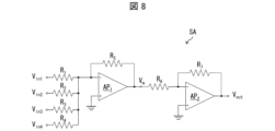
図1に図示した制御部14の一変形例について、図7及び図8を参照して説明する。図7の(a)及び(b)は、制御部14としてマイクロコンピュータの代わりに集積回路を用いる構成のブロック図である。図7の(a)及び(b)においては、光変調素子11aiの一例として光変調素子11a1を示し、イメージセンサ12aiの一例としてイメージセンサ12a1を示している。図8は、図7の(b)に示す加算回路SAの回路図である。
(Modification of the control unit)
A modified example of the
なお、図7の(a)では、光変調素子11a1の各セルCとイメージセンサ12a1の各受光セルPDCとが1対1対応している。一方、図7の(b)では、光変調素子11a1の各セルCとイメージセンサ12a1の各受光セルPDCとが1対4対応している。すなわち、図7の(b)における構成を図7の(a)における構成と比較した場合、イメージセンサ12a1における受光セルPDCの解像度は、縦及び横の各々について2倍であり、計4倍である。また、図7の(a)及び(b)において、互いに対向するセルCと受光セルPDCとの間に付した矢印は、互いに対向するセルCと受光セルPDCとが対向していることを表している。In FIG. 7(a), each cell C of the light modulation element 11a1 and each light receiving cell PDC of the image sensor 12a1 correspond one-to-one. On the other hand, in FIG. 7(b), each cell C of the light modulation element 11a1 and each light receiving cell PDC of the image sensor 12a1 correspond one-to-four. That is, when comparing the configuration in FIG. 7(b) with the configuration in FIG. 7(a), the resolution of the light receiving cell PDC in the image sensor 12a1 is twice as high vertically and horizontally, totaling four times. In addition, in FIG. 7(a) and (b), the arrows between the cell C and the light receiving cell PDC facing each other indicate that the cell C and the light receiving cell PDC facing each other are facing each other.
本変形例においては、光変調素子11a1の各セルCの位相変調量を、そのセルCに対応する受光セルPDCによって検出されたモニタ用信号光の強度に応じて設定する制御部14として、2つの抵抗Ra,Rbからなる分圧回路VDを用いている。分圧回路VDを用いることによって、受光セルPDCによって検出されたモニタ用信号光の強度に対応した電圧は、抵抗Ra,Rbの各々の抵抗値の比に応じて分圧され、Rb/(Ra+Rb)に対応する電圧がセルCに印加される。分圧回路VDからセルCに印加される当該電圧は、制御部14が設定する光変調素子11aiの各セルCの位相変調量Δφ(P)=P×α+βにおけるαに対応する。
In this modification, a voltage divider circuit VD consisting of two resistors Ra and Rb is used as the
例えば、光変調素子11a1が200×200個のセルCにより構成されており、イメージセンサ12a1が200×200個の受光セルPDCにより構成されている場合、光変調素子11a1及びイメージセンサ12a1に対応する制御部14は、200×200個の分圧回路VDを含む集積回路により構成される。For example, if the light modulation element 11a1 is composed of 200 x 200 cells C and the image sensor 12a1 is composed of 200 x 200 light receiving cells PDC, the
なお、光変調素子11a1の各セルCとイメージセンサ12a1の各受光セルPDCとがL対1対応している(すなわち、セルCがL個のサブセルにより構成されている)場合には、図7の(a)及び(b)に図示されている単一の分圧回路VDを、並列に設けられたL個の分圧回路に置換すればよい。各分圧回路は、セルCの各サブセルに対応するので、各分割回路により分圧された電圧は、セルCの各サブセルに印加される。このように、サブセル毎に対応する分圧回路を設けることにより、分圧されたうえで印加される電圧をサブセル毎に調整することができる。 Note that, when each cell C of the light modulation element 11a1 and each light receiving cell PDC of the image sensor 12a1 have an L-to-1 correspondence (i.e., cell C is composed of L subcells), the single voltage divider circuit VD shown in (a) and (b) of FIG. 7 can be replaced with L voltage divider circuits arranged in parallel. Each voltage divider circuit corresponds to a subcell of cell C, so that the voltage divided by each divider circuit is applied to each subcell of cell C. In this way, by providing a voltage divider circuit corresponding to each subcell, the voltage applied after voltage division can be adjusted for each subcell.
また、図7の(b)に示すように、光変調素子11a1の各セルCとイメージセンサ12a1の各受光セルPDCとが1対4対応している場合、各受光セルPDCは、サブ受光セルPDC1,PDC2と、図7の(b)に図示されていない2つのサブ受光セルにより構成される。この場合、セルCに対応する受光セルPDCによって検出されたモニタ用信号光の強度は、上述した4つのサブ受光セルによって検出されたモニタ用信号光の強度の平均で得られる。図7の(b)に示す構成では、4つのサブ受光セルによって検出されたモニタ用信号光の強度の平均を得るために加算回路SAを用いている。 Also, as shown in FIG. 7B, when each cell C of the light modulation element 11a1 and each light receiving cell PDC of the image sensor 12a1 correspond in a 1:4 ratio, each light receiving cell PDC is composed of sub light receiving cells PDC1 and PDC2 and two sub light receiving cells not shown in FIG. 7B. In this case, the intensity of the monitor signal light detected by the light receiving cell PDC corresponding to cell C is obtained by averaging the intensity of the monitor signal light detected by the above-mentioned four sub light receiving cells. In the configuration shown in FIG. 7B, an adder circuit SA is used to obtain the average intensity of the monitor signal light detected by the four sub light receiving cells.
加算回路SAは、図8に示すように、2個の増幅器AP1,AP2と、7個の抵抗R1~R7と、を備えている。本変形例では、抵抗R1~R4の抵抗値が等しく、R5はR1~R4の抵抗値の1/4の抵抗値、且つ、抵抗R6,R7の抵抗値が等しくなるように加算回路APを構成している。このように構成した加算回路APは、4つの入力ポートに4つのサブ受光セルによって検出されたモニタ用信号光の強度に対応する電圧Vin1~Vin4を入力した場合、中間ポートにおいて、Vm=-(Vin1+Vin2+Vin3+Vin4)/4 が得られ、出力ポートにおいて、Vout=(Vin1+Vin2+Vin3+Vin4)/4 が得られる。 8, the adder circuit SA includes two amplifiers AP1 and AP2 and seven resistors R1 to R7 . In this modification, the adder circuit AP is configured so that the resistance values of the resistors R1 to R4 are equal, the resistance value of R5 is 1/4 of the resistance values of R1 to R4 , and the resistance values of the resistors R6 and R7 are equal. When voltages Vin1 to Vin4 corresponding to the intensities of the monitor signal lights detected by the four sub-light receiving cells are input to the four input ports of the adder circuit AP configured in this way, Vm=-( Vin1 + Vin2 + Vin3 + Vin4 ) /4 is obtained at the intermediate port, and Vout=( Vin1 + Vin2 + Vin3 + Vin4 )/4 is obtained at the output port.
なお、本変形例では、イメージセンサ12aiとして、検出したモニタ用信号光の強度に対応した電圧を出力する受光セルPDCを含むイメージセンサを採用している。ただし、本発明の一態様においては、イメージセンサ12aiとして、検出したモニタ用信号光の強度に対応した電流(電荷)を出力する受光セルPDCを含むイメージセンサを採用することもできる。電圧を出力する受光セルPDCを含むイメージセンサの例としてはCMOSカメラが挙げられ、電流を出力する受光セルPDCを含むイメージセンサの例としてはCCDカメラが挙げられる。なお、電流を出力する受光セルPDCを含むイメージセンサを採用する場合、受光セルPDCの後段にトランスインピーダンスアンプを設け、出力された電流を電圧に変換すればよい。この構成によれば、電圧を出力する受光セルを採用する場合と同様に上述した分圧回路VD及び加算回路SAを適用することができる。In this modified example, an image sensor including a light receiving cell PDC that outputs a voltage corresponding to the intensity of the detected monitor signal light is used as the image sensor 12ai. However, in one aspect of the present invention, an image sensor including a light receiving cell PDC that outputs a current (charge) corresponding to the intensity of the detected monitor signal light can also be used as the image sensor 12ai. An example of an image sensor including a light receiving cell PDC that outputs a voltage is a CMOS camera, and an example of an image sensor including a light receiving cell PDC that outputs a current is a CCD camera. When using an image sensor including a light receiving cell PDC that outputs a current, a transimpedance amplifier can be provided in the rear stage of the light receiving cell PDC to convert the output current into a voltage. According to this configuration, the voltage divider circuit VD and the adder circuit SA described above can be applied in the same way as when a light receiving cell that outputs a voltage is used.
(まとめ)
本発明の態様1に係る光演算装置は、少なくとも1個の受光セルを含むイメージセンサと、位相変調量が互いに独立に設定可能な複数のセルを含む光変調素子と、信号光を前記イメージセンサに入射するモニタ用信号光と前記光変調素子に入射する演算用信号光とに分岐する光分岐素子と、前記光変調素子の各セルの位相変調量を、該セルに対応する前記イメージセンサの受光セルにて検出された前記モニタ用信号光の強度に応じて設定する制御部と、を備えている。
(summary)
The optical computing device according to
上記の構成によれば、光変調素子の各セルにおいて線形な位相変調を行う従来の光演算装置よりも多様な光演算を行うことができる。 With the above configuration, it is possible to perform more diverse optical calculations than conventional optical calculation devices that perform linear phase modulation in each cell of the optical modulation element.
本発明の態様2に係る光演算装置においては、態様1の構成に加えて、前記制御部は、前記光変調素子の各セルの位相変調量Δφ(P)を、Δφ(P)=P×α+βに従って設定する(ここで、Pは、該セルに対応する前記イメージセンサのセルにて検出された前記モニタ用信号光の強度であり、α及びβは、定数である)、という構成が採用されている。In the optical computing device according to aspect 2 of the present invention, in addition to the configuration of
上記の構成によれば、光変調素子の各セルにおいて線形な位相変調を行う従来の光演算装置よりも多様な光演算を行うことができる。 With the above configuration, it is possible to perform more diverse optical calculations than conventional optical calculation devices that perform linear phase modulation in each cell of the optical modulation element.
本発明の態様3に係る光演算装置においては、態様1又は2の構成に加えて、当該光演算装置は、前記光変調素子として、複数の反射型の光変調素子を備え、前記モニタ用信号光は、前記光分岐素子を透過した信号光であり、前記演算用信号光は、前記光分岐素子に反射された信号光である、という構成が採用されている。In the optical arithmetic device according to aspect 3 of the present invention, in addition to the configuration of
上記の構成によれば、反射型の光変調素子を用いて、多段の光演算を行うことができる。 According to the above configuration, multi-stage optical calculations can be performed using a reflective optical modulation element.
本発明の態様4に係る光演算装置においては、態様3の構成に加えて、前記複数の反射型の光変調素子は、一体化されている、という構成が採用されている。In the optical computing device according to aspect 4 of the present invention, in addition to the configuration of aspect 3, the multiple reflective optical modulation elements are integrated.
上記の構成によれば、光演算装置の部品点数を少なく抑えることができる。また、複数の反射型の光変調素子が別体である場合に必要になる、反射型の光変調素子間のアライメント調整を省略することができる。 According to the above configuration, the number of parts of the optical computing device can be reduced. In addition, it is possible to omit alignment adjustment between the reflective optical modulation elements, which is necessary when multiple reflective optical modulation elements are separate.
本発明の態様5に係る光演算装置においては、態様1又は2の構成に加えて、当該光演算装置は、前記光変調素子として、複数の透過型の光変調素子を備え、前記モニタ用信号光は、前記光分岐素子に反射された信号光であり、前記演算用信号光は、前記光分岐素子を透過した信号光である、という構成が採用されている。In the optical arithmetic device according to aspect 5 of the present invention, in addition to the configuration of
上記の構成によれば、透過型の光変調素子を用いて、多段の光演算を行うことができる。 According to the above configuration, multi-stage optical calculations can be performed using a transmissive optical modulation element.
本発明の態様6に係る光演算装置においては、態様1~5の何れかの構成に加えて、当該光演算装置は、前記光変調素子、前記イメージセンサ、及び前記光分岐素子の組み合わせを複数段備え、2段目以降の各段の前記光分岐素子には、該段の前段の光変調素子にて生成された信号光が入力される、という構成が採用されている。In the optical computing device according to aspect 6 of the present invention, in addition to the configuration of any one of
上記の構成によれば、多段の光演算を行うことができる。 With the above configuration, multi-stage optical calculations can be performed.
本発明の態様7に係る光演算装置においては、態様1~6の何れかの構成に加えて、前記制御部は、前記光変調素子の全てのセルの位相変調量が一定の値に収束した後、正しい演算結果を表す信号光が出力されていることを示す信号を出力する、という構成が採用されている。In the optical arithmetic device according to aspect 7 of the present invention, in addition to the configuration of any one of
上記の構成によれば、上記信号の出力先において、光変調素子の全てのセルの位相変調量が一定の値に収束する前に当該光演算装置から出力され得る、正しくない演算結果を表す信号光が参照されるリスクを低減することができる。 With the above configuration, the risk of the signal output destination referring to signal light representing an incorrect calculation result, which may be output from the optical calculation device before the phase modulation amounts of all cells of the optical modulation element converge to a certain value, can be reduced.
本発明の態様8に係る制御方法は、少なくも1個の受光セルを含むイメージセンサと、位相変調量が互いに独立に設定可能な複数のセルを含む光変調素子と、信号光を前記イメージセンサに入射するモニタ用信号光と前記光変調素子に入射する演算用信号光とに分岐する光分岐素子と、を備えた光演算装置の制御方法であって、前記光変調素子の各セルの位相変調量を、該セルに対応する前記イメージセンサの受光セルにて検出された前記モニタ用信号光の強度に応じて設定する工程を含む。 The control method according to aspect 8 of the present invention is a control method for an optical arithmetic device comprising an image sensor including at least one light receiving cell, an optical modulation element including a plurality of cells whose phase modulation amounts can be set independently of each other, and an optical branching element that branches signal light into a monitor signal light that is incident on the image sensor and an arithmetic signal light that is incident on the optical modulation element, and includes a step of setting the phase modulation amount of each cell of the optical modulation element according to the intensity of the monitor signal light detected by the light receiving cell of the image sensor corresponding to that cell.
上記の方法によれば、光変調素子の各セルにおいて線形な位相変調を行う従来の光演算装置よりも多様な光演算を行うことができる。 The above method makes it possible to perform more diverse optical calculations than conventional optical calculation devices that perform linear phase modulation in each cell of the optical modulation element.
(付記事項)
本発明は、上述した各実施形態に限定されるものでなく、請求項に示した範囲で種々の変更が可能である。上述した実施形態に含まれる各技術的手段を適宜組み合わせて得られる実施形態についても、本発明の技術的範囲に含まれる。
(Additional Notes)
The present invention is not limited to the above-described embodiments, and various modifications are possible within the scope of the claims. Embodiments obtained by appropriately combining the technical means included in the above-described embodiments are also included in the technical scope of the present invention.
1 光演算装置
11 光変調素子群
11a1~11an 光変調素子(反射型)
11b1~11bn 光変調素子(透過型)
12 イメージセンサ群
12a1~12an イメージセンサ
13 光分岐素子群
13a1~13an 光分岐素子
1 Optical
11b1 to 11bn: Light modulation element (transmissive type)
12 Image sensor group 12a1 to
Claims (8)
位相変調量が互いに独立に設定可能な複数のセルを含む光変調素子と、
信号光を前記イメージセンサに入射するモニタ用信号光と前記光変調素子に入射する演算用信号光とに分岐する光分岐素子と、
前記光変調素子の各セルの位相変調量を、該セルに対応する前記イメージセンサの受光セルにて検出された前記モニタ用信号光の強度に応じて設定する制御部と、を備えている、
ことを特徴とする光演算装置。 an image sensor including at least one light receiving cell;
an optical modulation element including a plurality of cells whose phase modulation amounts can be set independently of each other;
an optical branching element that branches a signal light into a monitor signal light that is incident on the image sensor and an arithmetic signal light that is incident on the optical modulation element;
a control unit that sets the amount of phase modulation of each cell of the light modulation element in accordance with the intensity of the monitor signal light detected by a light receiving cell of the image sensor corresponding to the cell.
An optical computing device comprising:
ことを特徴とする請求項1に記載の光演算装置。 The control unit sets the phase modulation amount Δφ(P) of each cell of the light modulation element according to Δφ(P)=P×α+β (where P is the intensity of the monitor signal light detected by the light receiving cell of the image sensor corresponding to the cell, and α and β are constants);
2. The optical computing device according to claim 1 .
前記モニタ用信号光は、前記光分岐素子を透過した信号光であり、
前記演算用信号光は、前記光分岐素子に反射された信号光である、
ことを特徴とする請求項1又は2に記載の光演算装置。 The optical arithmetic device includes a plurality of reflective optical modulation elements as the optical modulation elements,
the monitor signal light is a signal light transmitted through the optical branching element,
the calculation signal light is signal light reflected by the optical branching element,
3. The optical computing device according to claim 1, wherein the optical computing device is a first optical computing device.
ことを特徴とする請求項3に記載の光演算装置。 The plurality of reflective light modulation elements are integrated together.
4. The optical computing device according to claim 3.
前記モニタ用信号光は、前記光分岐素子に反射された信号光であり、
前記演算用信号光は、前記光分岐素子を透過した信号光である、
ことを特徴とする請求項1又は2に記載の光演算装置。 The optical arithmetic device includes a plurality of transmissive optical modulation elements as the optical modulation elements,
the monitor signal light is a signal light reflected by the optical branching element,
the calculation signal light is a signal light transmitted through the optical branching element,
3. The optical computing device according to claim 1, wherein the optical computing device is a first optical computing device.
2段目以降の各段の前記光分岐素子には、該段の前段の光変調素子にて生成された信号光が入力される、
ことを特徴とする請求項1又は2に記載の光演算装置。 The optical calculation device includes a plurality of stages each including a combination of the optical modulation element, the image sensor, and the optical branching element,
The optical branching element of each stage from the second stage onward receives the signal light generated by the optical modulation element of the previous stage.
3. The optical computing device according to claim 1, wherein the optical computing device is a first optical computing device.
ことを特徴とする請求項1又は2に記載の光演算装置。 the control unit outputs a signal indicating that a signal light representing a correct calculation result is being output after the phase modulation amounts of all the cells of the optical modulation element have converged to a constant value.
3. The optical computing device according to claim 1, wherein the optical computing device is a first optical computing device.
前記光変調素子の各セルの位相変調量を、該セルに対応する前記イメージセンサの受光セルにて検出された前記モニタ用信号光の強度に応じて設定する工程を含む、
ことを特徴とする光演算装置の制御方法。 A method for controlling an optical arithmetic device including an image sensor including at least one light receiving cell, an optical modulation element including a plurality of cells whose phase modulation amounts can be set independently of each other, and an optical branching element that branches a signal light into a monitor signal light incident on the image sensor and an arithmetic signal light incident on the optical modulation element, comprising:
setting an amount of phase modulation of each cell of the light modulation element in accordance with an intensity of the monitor signal light detected by a light receiving cell of the image sensor corresponding to the cell;
23. A method for controlling an optical computing device comprising:
Applications Claiming Priority (3)
| Application Number | Priority Date | Filing Date | Title |
|---|---|---|---|
| JP2022025020 | 2022-02-21 | ||
| JP2022025020 | 2022-02-21 | ||
| PCT/JP2023/003772 WO2023157694A1 (en) | 2022-02-21 | 2023-02-06 | Optical arithmetic device and method for controlling optical arithmetic device |
Publications (3)
| Publication Number | Publication Date |
|---|---|
| JPWO2023157694A1 JPWO2023157694A1 (en) | 2023-08-24 |
| JPWO2023157694A5 JPWO2023157694A5 (en) | 2024-09-13 |
| JP7624552B2 true JP7624552B2 (en) | 2025-01-30 |
Family
ID=87578598
Family Applications (1)
| Application Number | Title | Priority Date | Filing Date |
|---|---|---|---|
| JP2024501299A Active JP7624552B2 (en) | 2022-02-21 | 2023-02-06 | Optical arithmetic device and method for controlling optical arithmetic device |
Country Status (5)
| Country | Link |
|---|---|
| US (1) | US20250155735A1 (en) |
| EP (1) | EP4485121A4 (en) |
| JP (1) | JP7624552B2 (en) |
| CN (1) | CN118696286A (en) |
| WO (1) | WO2023157694A1 (en) |
Citations (2)
| Publication number | Priority date | Publication date | Assignee | Title |
|---|---|---|---|---|
| JP2007171422A (en) | 2005-12-20 | 2007-07-05 | Fujikura Ltd | OPTICAL ELEMENT AND OPTICAL MODULATOR HAVING OPTICAL ELEMENT |
| JP2009246578A (en) | 2008-03-31 | 2009-10-22 | Yokogawa Electric Corp | Optical transmission device, and optical test device |
Family Cites Families (4)
| Publication number | Priority date | Publication date | Assignee | Title |
|---|---|---|---|---|
| US7847225B2 (en) | 2008-05-02 | 2010-12-07 | Hiroshima University | Optical neural network |
| JP5814201B2 (en) * | 2012-09-10 | 2015-11-17 | 日本電信電話株式会社 | High-speed chaotic optical signal generation optical circuit |
| KR102783990B1 (en) * | 2019-01-24 | 2025-03-24 | 삼성전자주식회사 | Optical neural network apparatus including passive phase modulator |
| US11574178B2 (en) * | 2020-03-11 | 2023-02-07 | Lighton | Method and system for machine learning using optical data |
-
2023
- 2023-02-06 WO PCT/JP2023/003772 patent/WO2023157694A1/en not_active Ceased
- 2023-02-06 US US18/839,586 patent/US20250155735A1/en active Pending
- 2023-02-06 CN CN202380021570.6A patent/CN118696286A/en active Pending
- 2023-02-06 JP JP2024501299A patent/JP7624552B2/en active Active
- 2023-02-06 EP EP23756221.0A patent/EP4485121A4/en active Pending
Patent Citations (2)
| Publication number | Priority date | Publication date | Assignee | Title |
|---|---|---|---|---|
| JP2007171422A (en) | 2005-12-20 | 2007-07-05 | Fujikura Ltd | OPTICAL ELEMENT AND OPTICAL MODULATOR HAVING OPTICAL ELEMENT |
| JP2009246578A (en) | 2008-03-31 | 2009-10-22 | Yokogawa Electric Corp | Optical transmission device, and optical test device |
Also Published As
| Publication number | Publication date |
|---|---|
| CN118696286A (en) | 2024-09-24 |
| US20250155735A1 (en) | 2025-05-15 |
| EP4485121A1 (en) | 2025-01-01 |
| JPWO2023157694A1 (en) | 2023-08-24 |
| WO2023157694A1 (en) | 2023-08-24 |
| EP4485121A4 (en) | 2026-03-04 |
Similar Documents
| Publication | Publication Date | Title |
|---|---|---|
| CN111753977A (en) | Optical neural network convolution layer chip, convolution computing method and electronic device | |
| CN113805641B (en) | Photonic neural network | |
| CN118414570A (en) | Optical transmission path and optical connector | |
| CN117157617A (en) | Apparatus and method for performing arithmetic operations | |
| Piao et al. | Programmable photonic time circuits for highly scalable universal unitaries | |
| Dey et al. | All-optical integrated square root of Pauli-Z (SRZ) gates using polarization and phase encoding | |
| JP7624552B2 (en) | Optical arithmetic device and method for controlling optical arithmetic device | |
| CN113589435B (en) | A fully passive polarization quantum state tomography method and chip | |
| Ma et al. | Magneto-optics enhances in-memory computing | |
| CN215181644U (en) | Integrated light source and control NOT gate optical quantum computing chip and teaching system using the same | |
| CN110275365A (en) | A kind of full light four of binary system selects a data selector | |
| Raja et al. | Ultra-high-speed all-optical multivalued inverter using nonlinear polarization rotation in semiconductor optical amplifier | |
| US20260016850A1 (en) | Optical computation device | |
| Xu et al. | High-energy-efficiency integrated photonic convolutional neural networks | |
| JPWO2024024414A5 (en) | ||
| JP7741990B2 (en) | Optical arithmetic device, learning method for optical arithmetic device, and manufacturing method for optical arithmetic device | |
| Liu et al. | Ultra-compact universal linear-optical logic gate based on single rectangle plasmonic slot nanoantenna | |
| Ma et al. | Photonics multiply-accumulation computations system based on residue arithmetic | |
| JP7745655B2 (en) | Optical computing device and optical computing method | |
| Liu et al. | Non-Hermitian optical scattering in cold atoms via four-wave mixing | |
| CN119164501B (en) | A balanced homodyne detection device based on intensity modulation | |
| US20240353887A1 (en) | Optical computing device, optical computing method, and manufacturing method for optical computing device | |
| Batabyal et al. | Design of dibit based all optical frequency encoded controlled Fredkin gate using optical switches | |
| CN120235203A (en) | Optoelectronic neurons and photonic computing units | |
| Yang et al. | Dual-function electro-optical modulation for fully hardware-implemented photonic restricted Boltzmann machine |
Legal Events
| Date | Code | Title | Description |
|---|---|---|---|
| A521 | Request for written amendment filed |
Free format text: JAPANESE INTERMEDIATE CODE: A523 Effective date: 20240702 |
|
| A621 | Written request for application examination |
Free format text: JAPANESE INTERMEDIATE CODE: A621 Effective date: 20240702 |
|
| TRDD | Decision of grant or rejection written | ||
| A01 | Written decision to grant a patent or to grant a registration (utility model) |
Free format text: JAPANESE INTERMEDIATE CODE: A01 Effective date: 20250107 |
|
| A61 | First payment of annual fees (during grant procedure) |
Free format text: JAPANESE INTERMEDIATE CODE: A61 Effective date: 20250120 |
|
| R150 | Certificate of patent or registration of utility model |
Ref document number: 7624552 Country of ref document: JP Free format text: JAPANESE INTERMEDIATE CODE: R150 |