JP7620105B2 - Method for manufacturing a luminous needle - Google Patents
Method for manufacturing a luminous needle Download PDFInfo
- Publication number
- JP7620105B2 JP7620105B2 JP2023534921A JP2023534921A JP7620105B2 JP 7620105 B2 JP7620105 B2 JP 7620105B2 JP 2023534921 A JP2023534921 A JP 2023534921A JP 2023534921 A JP2023534921 A JP 2023534921A JP 7620105 B2 JP7620105 B2 JP 7620105B2
- Authority
- JP
- Japan
- Prior art keywords
- light
- optical material
- material layer
- refractive index
- layer
- Prior art date
- Legal status (The legal status is an assumption and is not a legal conclusion. Google has not performed a legal analysis and makes no representation as to the accuracy of the status listed.)
- Active
Links
Images


Classifications
-
- G—PHYSICS
- G04—HOROLOGY
- G04B—MECHANICALLY-DRIVEN CLOCKS OR WATCHES; MECHANICAL PARTS OF CLOCKS OR WATCHES IN GENERAL; TIME PIECES USING THE POSITION OF THE SUN, MOON OR STARS
- G04B19/00—Indicating the time by visual means
- G04B19/04—Hands; Discs with a single mark or the like
- G04B19/042—Construction and manufacture of the hands; arrangements for increasing reading accuracy
-
- G—PHYSICS
- G04—HOROLOGY
- G04B—MECHANICALLY-DRIVEN CLOCKS OR WATCHES; MECHANICAL PARTS OF CLOCKS OR WATCHES IN GENERAL; TIME PIECES USING THE POSITION OF THE SUN, MOON OR STARS
- G04B19/00—Indicating the time by visual means
- G04B19/30—Illumination of dials or hands
- G04B19/32—Illumination of dials or hands by luminescent substances
-
- G—PHYSICS
- G04—HOROLOGY
- G04B—MECHANICALLY-DRIVEN CLOCKS OR WATCHES; MECHANICAL PARTS OF CLOCKS OR WATCHES IN GENERAL; TIME PIECES USING THE POSITION OF THE SUN, MOON OR STARS
- G04B45/00—Time pieces of which the indicating means or cases provoke special effects, e.g. aesthetic effects
- G04B45/0007—Light-, colour-, line-, or spot-effects caused by parts or pictures moved by the clockwork
Landscapes
- Physics & Mathematics (AREA)
- General Physics & Mathematics (AREA)
- Engineering & Computer Science (AREA)
- Manufacturing & Machinery (AREA)
- Illuminated Signs And Luminous Advertising (AREA)
- Light Guides In General And Applications Therefor (AREA)
- Details Of Measuring Devices (AREA)
- Led Device Packages (AREA)
Description
本発明は、発光針の分野に関し、より詳細には、発光針の製造に関する。 The present invention relates to the field of luminous needles, and more particularly to the manufacture of luminous needles.
時計ムーブメント用の針を作製するにはいくつかの方法がある。 There are several ways to make hands for a clock movement.
それにも関わらず、これらの方法は発光針の製造には適していない。なぜなら、発光針は、光を少量しか返さなかったり、光の大部分を一点に集中させたりすることがあまりにも多く、必ずしも出願人によって求められる効果ではないからである。 Nonetheless, these methods are not suitable for producing luminous needles, since they too often return only a small amount of light or concentrate most of the light at a single point, which is not necessarily the effect desired by the applicant.
実際、一部の製造方法では、光が発光針の1つの面でしか抽出されなかったり、または内側に反射されたりするため、発光針の輝度は低くなる。 In fact, some manufacturing methods result in a less bright needle because light is only extracted from one side of the needle or is reflected inward.
本発明は、時計ムーブメント用の、好ましくは腕時計用の少なくとも1つの発光針を製造するための方法のおかげで、前述した欠点のすべてまたは一部を解決することを目的としており、前記製造方法は少なくとも1つ、
少なくとも1つの支持体を準備することであって、前記少なくとも1つの支持体は少なくとも1つの光ガイドを備えており、前記少なくとも1つの光ガイドは少なくとも1つの出射面を備えており、光を導くように構成されている、準備することと、
前記少なくとも1つの出射面を構造化することとを含んでいる。
The present invention aims to overcome all or part of the aforementioned drawbacks by virtue of a method for manufacturing at least one luminous hand for a timepiece movement, preferably for a wristwatch, said manufacturing method comprising at least one:
providing at least one support, the at least one support comprising at least one light guide, the at least one light guide comprising at least one exit surface and configured to guide light;
and structuring the at least one exit surface.
この構成のおかげで、配光を有する時計ムーブメント用の発光針を製造することが可能である。 Thanks to this configuration, it is possible to produce luminous hands for watch movements with light distribution.
1つの実施形態によれば、前記少なくとも1つの構造化は、研磨によって、アブレーションによって、サンドブラストによって、スタンピングおよび/または光での構築によって実行される。 According to one embodiment, said at least one structuring is carried out by polishing, by ablation, by sandblasting, by stamping and/or by photostructuring .
この構成のおかげで、前記少なくとも1つの出射面を増やすことによって、光を分配することが可能である。 Thanks to this configuration, it is possible to distribute the light by increasing the number of said at least one exit surface.
1つの実施形態によれば、少なくとも1つの支持体の前記少なくとも1つの準備は、少なくとも1つの第1の光学物質層の堆積を含んでおり、前記少なくとも1つの第1の光学物質層は、第1の屈折率を有している。 According to one embodiment, the at least one preparation of the at least one support includes deposition of at least one first optical material layer, the at least one first optical material layer having a first refractive index.
1つの実施形態によれば、前記少なくとも1つの第1の光学物質層の前記堆積は、熱処理ステップを含んでいる。 According to one embodiment, the deposition of the at least one first optical material layer includes a heat treatment step.
これら前述した構成のうちの何れかのおかげで、反射層を有する発光針を製造することが可能である。 Thanks to any of these aforementioned configurations, it is possible to manufacture a luminous needle with a reflective layer.
1つの実施形態によれば、少なくとも1つの支持体の前記少なくとも1つの準備は、少なくとも1つの発光物質層の少なくとも1つの堆積を含んでいる。 According to one embodiment, the at least one preparation of the at least one support comprises at least one deposition of at least one luminescent material layer.
この構成のおかげで、発光針を製造することが可能である。 Thanks to this configuration, it is possible to produce luminous needles.
1つの実施形態によれば、少なくとも1つの支持体の前記少なくとも1つの準備は、少なくとも1つの第2の光学物質層の堆積を含んでおり、前記少なくとも1つの第2の光学物質層は、第2の屈折率を有している。 According to one embodiment, the at least one preparation of the at least one support includes deposition of at least one second optical material layer, the at least one second optical material layer having a second refractive index.
1つの実施形態によれば、前記第1の屈折率は、前記第2の屈折率よりも低い。 According to one embodiment, the first refractive index is lower than the second refractive index.
この構成のおかげで、光を前記少なくとも1つの出射面に向かって屈折させることが可能である。 Thanks to this configuration, it is possible to refract light towards at least one of the exit surfaces.
本発明は、少なくとも1つ、
支持体であって、前記少なくとも1つの支持体は、針を形成するように構成されている、支持体と、
光ガイドであって、前記少なくとも1つの光ガイドは、前記少なくとも1つの光ガイドから光を抽出するために、粗く構成された少なくとも1つの出射面を備えている、光ガイドと、を備えている少なくとも1つの発光針によって、前述した欠点のすべてまたは一部を解決することを目的としている。
The present invention comprises at least one
a support, the at least one support being configured to form a needle;
The aim of the present invention is to overcome all or part of the aforementioned drawbacks by at least one light emitting needle comprising a light guide, the at least one light guide having at least one exit surface that is roughly configured to extract light from the at least one light guide.
この構成のおかげで、前記少なくとも1つの出射面から、最大の光を抽出できる少なくとも1つの発光針を有することが可能である。 Thanks to this configuration, it is possible to have at least one light emitting needle capable of extracting maximum light from the at least one exit surface.
1つの実施形態によれば、前記少なくとも1つの光ガイドは、第1の屈折率を有している少なくとも1つの第1の光学物質層と、第2の屈折率を有している少なくとも1つの第2の光学物質層とを備えており、前記第1の屈折率は、前記第2の屈折率よりも低い。 According to one embodiment, the at least one light guide comprises at least one first optical material layer having a first refractive index and at least one second optical material layer having a second refractive index, the first refractive index being lower than the second refractive index.
この構成のおかげで、前記少なくとも1つの出射面に向かって光を導くことが可能である。 Thanks to this configuration, it is possible to guide light toward at least one of the exit surfaces.
本発明は、決して限定するものではない例として与えられる添付の図面を使用して、以下に、より詳細に説明される。 The invention will now be explained in more detail using the accompanying drawings, given as a non-limiting example:
いくつかのタイプの発光針が市販されている。それにも関わらず、出願人は、新世代の発光針を提案する。 Several types of luminous needles are available on the market. Nevertheless, the applicant proposes a new generation of luminous needles.
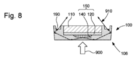
実際、出願人は、図8に見られるように、針を形成するように構成された少なくとも1つの支持体110と、少なくとも1つの光ガイド150から光910を抽出するために、粗く構成された少なくとも1つの出射面190を備えている前記少なくとも1つの光ガイド150とを備えている、少なくとも1つの発光針100を提案する。
Indeed, the applicant proposes at least one
前記少なくとも1つの発光針100は、時計ムーブメントにおいて、好ましくは腕時計のために使用されることを意図されており、出願人の製造方法500のおかげで取得され得る。この目的のために、前記製造方法は、図1に示すように、少なくとも1つの支持体110、好ましくは金属板110の少なくとも1つの準備510を含んでいる。
Said at least one
前記少なくとも1つの支持体110は、堆積520中に、少なくとも1つの第1の光学物質層120、好ましくは、第1の屈折率を有する少なくとも1つの光学絶縁層を受け取り、その後決定された温度521における熱処理525を経て、光が前記金属板110によって吸収されることを防止することを可能にする。前記少なくとも1つの第1の光学物質層120の前記堆積520の前に、前記金属板110または前記少なくとも1つの支持体110は、洗浄されるか、または洗浄後、前記少なくとも1つの第1の光学物質層120の接着を促進するためにプラズマ処理が適用され得る。この場合、前記少なくとも1つの第1の光学物質層120は、たとえば、POLYRISETM社によって商品化されている樹脂であってもよく、前記少なくとも1つの支持体110の表面を光学的に分離して、光の吸収をできるだけ少なくすることが目的とされている。この光学的分離は、1.60、特に1.45、好ましくは1.35を超えることがない前記第1の屈折率のおかげで可能となる。
The at least one
前記少なくとも1つの第1の光学物質層120は、たとえば印刷またはスプレーによって堆積され得る。なぜなら、スプレーは、前記少なくとも1つの第1の光学物質層120を有用な部分上に選択的に堆積させ、無駄を回避することを可能にするからである。
The at least one first
前述したように、前記少なくとも1つの第1の光学物質層120は、前記少なくとも1つの第1の光学物質層120の溶媒が蒸発できるように、たとえば窒素下で300℃で1時間、前記熱処理525を受け、これは図2で確認することができる。
As previously mentioned, the at least one first
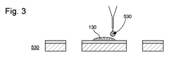
図3に示すように、少なくとも1つの発光物質層130の少なくとも1つの堆積530は、前記少なくとも1つの支持体110上、好ましくは前記少なくとも1つの第1の光学物質層120上で実行され得る。前記少なくとも1つの発光物質層130は、好ましくは蛍光顔料と、重合による取り付けを可能にする接着剤とを含み、前記少なくとも1つの発光物質層130が、たとえば、530nm未満の波長範囲を有する光源によって照明されるときに、前記少なくとも1つの発光針100を照明するように意図されている。
As shown in FIG. 3, at least one
実際、蛍光顔料は、二次蛍光の光源となる可能性がある。腕時計では、蛍光顔料は、たとえば青色または紫外光の光源によって遠隔から励起することができる。スクリーン印刷またはデジタル印刷などの他の技法が、前記少なくとも1つの発光物質層130の前記少なくとも1つの堆積530に使用できることに留意されたい。
In fact, fluorescent pigments can be the source of secondary fluorescence. In a watch, the fluorescent pigments can be excited remotely, for example by a source of blue or ultraviolet light. It should be noted that other techniques, such as screen printing or digital printing, can be used for the at least one
その後、たとえばMICRORESIST TECHNOLOGYTM社のORMOCLEAR(登録商標)10樹脂タイプの第2の光学物質140の少なくとも一層の接着を促進するために、数分間のUVプラズマ処理が行われるが、これは、ロッドコーティングによって、またはたとえば、図4に示されるように、スプレッドコーティングと言い換えることができるドクターブレードタイプの堆積540によって行われる。
This is followed by a few minutes of UV plasma treatment to promote adhesion of at least one layer of a second
さらに図4を参照して示すように、前記少なくとも1つの第2の光学物質層140が、ブレードによって押されて、存在する可能性のある様々なキャビティを充填できることが観察できる。
As further shown with reference to FIG. 4, it can be observed that the at least one second
前記少なくとも1つの第2の光学物質層140は、前記少なくとも1つの発光物質層130によって放射される蛍光を導くために、前記第1の屈折率よりも大きな第2の屈折率を有していることに留意されたい。
It should be noted that the at least one second
図5に見られるように、前記少なくとも1つの第2の光学物質層140は、真空551下における紫外光552の照射によって固定され得る。あるいは、紫外光下での照射前に空気を追い出すために、プラスチックフィルムをラミネートすることも可能であり得る。
As seen in FIG. 5, the at least one second
実際、前記少なくとも1つの第2の光学物質層140の下面は、前記少なくとも1つの発光物質層130との光学的接触を確立するために、光源900の反対側に蛍光物質の1つまたは複数の堆積物を含んでおり、前述したように、少なくとも1つの発光物質層130は、接着剤に含有された蛍光顔料で形成することができる。あるいは、蛍光物質を、導光層に埋め込んでもよい。
In fact, the underside of the at least one second
動作中、光源900は、前記少なくとも1つの発光物質層130によって再び放射される波長よりも短い波長を有する、前記少なくとも1つの発光物質層130を照明する。前記少なくとも1つの発光物質層130は、特に、前記少なくとも1つの第2の光学物質層140において、この入射光を吸収し、再び放射910する。前記少なくとも1つの第1の光学物質層120の存在により、前記少なくとも1つの第2の光学物質層140内を伝播する蛍光の内部全反射が可能になり、したがって、前記少なくとも1つの支持体110内での漸進的な吸収が回避される。
During operation, the
前記少なくとも1つの支持体110と前記少なくとも1つの第2の光学物質層140との間の屈折率の差は、0.5から0.9、好ましくは0.55から0.8、より好ましくは0.6から0.75の範囲内に含まれており、蛍光の結合を最大化するために、臨界角の値、したがって、前記少なくとも1つの第2の光学物質層140の開口数を増加させることが可能となる。前記少なくとも1つの第1の光学物質層120の存在により、ひとたび光が結合された後は、前記少なくとも1つの第2の光学物質層140における無損失の透過が可能になり、前記少なくとも1つの第1の光学物質層120の屈折率が、結合される光の量に影響を与えることに留意されたい。前記少なくとも1つの第1の光学物質層120は、2μmから15μm、好ましくは3μmから12μm、さらにより好ましくは5μmから10μmの範囲内の厚さを有することができる。前記少なくとも1つの第2の光学物質層140における多数の全反射は、光束が外側に伝達される前記少なくとも1つの発光針100の一端に到達するまで続く。
The difference in refractive index between the at least one
最後に、図6に概略的に示される、前記少なくとも1つの出射面190を構造化するステップ560は、前記少なくとも1つの出射面190を、および/または、たとえば、再屈折して光の大部分が一点に集中することになる全体的にまたは部分的に逃げる光910を、増加させるために、研磨565によって、アブレーション565によって、サンドブラスト565によって、スタンピング565および/または光での構築565によって実行され得る。実際、表面構造は、つまり前記少なくとも1つの第2の光学物質層140の前記少なくとも1つの出射面190上に、粗さを誘発するために局所的に剥離され得る前記少なくとも1つの第2の光学物質層140の物質のために設けられ得、これによって、第2の光学物質層140からの光910の抽出が容易になる。
Finally, a
それに加えて、樹脂の堆積によって作製することができる光拡散領域を、前記少なくとも1つの発光針100に追加して、発光針100は、光束の漏れを容易にするために、および、前記先端に装飾パターンを得るために、前記少なくとも1つの支持体110を越えて延在させる、すなわち、前記少なくとも1つの支持体110から突出させる。図示されていない実施形態によれば、前記少なくとも1つの発光針100の先端だけでなく、前記少なくとも1つの発光針100の縁部、および場合によっては頭部も、前記少なくとも1つの出射面190を構成する。
In addition, a light-diffusing area, which can be made by deposition of resin, is added to the at least one
前記少なくとも1つの発光針100を切断するステップ570は、たとえばレーザ571によって実行されることが好ましい。なぜなら、レーザ571は、前記少なくとも1つの第1の光学物質層120と、少なくとも1つの第2の光学物質層140とから構成される、前記少なくとも1つの光ガイド150を溶融し、前記少なくとも1つの光ガイド150の内側に向かって光910を反射させることを可能にする、図7の研磨された表面状態を生成することができるためである。
The
図8の例では、前記少なくとも1つの発光針100の輪郭を照明するために、前記少なくとも1つの出射面190は、前記少なくとも1つの発光針100の周面に対応する。実際、前記少なくとも1つの発光物質層130が、330nmと560nmとの間に含まれる波長を有する前記光源900に曝されると、前記少なくとも1つの発光物質層130は、前記少なくとも1つの光ガイド150の前記少なくとも1つの出射面190を介して抽出される前記光910を生成する。もちろん、たとえば、回転軸の近くまたは回転軸から離れた場所など、検討中の製品に適した場所に光源LEDを配置し、前記光源900の光束を、適切な場所に移動させて、前記少なくとも1つの発光針100の蛍光物質を励起させることを可能にする光カプラを追加することも可能である。したがって、従来技術とは異なり、前記光源900は、前記少なくとも1つの発光針100上に配置されない。
In the example of FIG. 8, the at least one
Claims (7)
前記発光針(100)を支持する少なくとも1つの支持体(110)を準備すること(510)と、
少なくとも1つの出射面(190)を備えており、光(910)を導くように構成されている光ガイド(150)を、この少なくとも1つの支持体(110)上に形成することとを含み、この形成ステップは、以下のサブステップ、すなわち、
第1の屈折率を有しており、前記光が前記支持体(110)によって吸収されることを防止することができる、少なくとも1つの第1の光学物質層(120)の、前記支持体(110)上の堆積(520)と、
少なくとも1つの発光物質層(130)の、少なくとも1つの前記第1の光学物質層(120)上の堆積(530)と、
少なくとも1つの第2の光学物質層(140)の堆積(540)であって、少なくとも1つの前記第2の光学物質層(140)は、第2の屈折率を有している、堆積(540)と、
少なくとも1つの前記光ガイド(150)から前記光(910)を抽出するために、この出射面(190)が粗くなるように、少なくとも1つの前記出射面(190)を構築すること(560)とを含んでいる、製造方法(500)。 A method (500) for manufacturing at least one luminous hand (100) for a timepiece movement, said method (500) comprising :
Providing (510) at least one support (110) for supporting said light emitting needle (100);
forming, on the at least one support (110), a light guide (150) having at least one exit surface (190) and configured to guide light (910), the forming step comprising the following sub-steps:
Deposition (520) of at least one first optical material layer (120) on the support (110), the first optical material layer (120) having a first refractive index and capable of preventing the light from being absorbed by the support (110);
depositing (530) at least one layer of luminescent material (130) on the at least one layer of first optical material (120);
depositing (540) at least one layer of a second optical material (140), the at least one layer of the second optical material (140) having a second refractive index;
and structuring (560) at least one exit surface (190) such that the exit surface (190) is roughened to extract the light (910) from the at least one light guide (150).
前記発光針を支持する支持体(110)と、
光ガイド(150)であって、少なくとも1つの前記光ガイド(150)は、少なくとも、
第1の屈折率を有しており、光が前記支持体(110)によって吸収されるのを防止することができる、第1の光学物質層(120)と、
少なくとも1つの前記第1の光学物質層(120)上の発光物質層(130)と、
第2の屈折率を有しており、少なくとも1つの前記光ガイド(150)から前記光(910)を抽出するために、粗く構成されている出射面(190)を備えた第2の光学物質層(140)とを備えている、光ガイド(150)とを備えている、発光針(100)。 A luminous hand (100) for a clock movement , comprising:
A support (110) for supporting the luminous needle;
A light guide (150), wherein at least one of the light guides (150) comprises at least
a first optical material layer (120) having a first refractive index and capable of preventing light from being absorbed by the support (110);
a layer of luminescent material (130) on at least one of the first optical material layers (120);
and a second optical material layer (140) having a second refractive index and having an exit surface (190) that is configured to be rough for extracting the light (910) from at least one of the light guides (150).
Applications Claiming Priority (3)
| Application Number | Priority Date | Filing Date | Title |
|---|---|---|---|
| EP20213515.8 | 2020-12-11 | ||
| EP20213515 | 2020-12-11 | ||
| PCT/EP2021/074292 WO2022122199A1 (en) | 2020-12-11 | 2021-09-02 | Method for manufacturing luminescent hands |
Publications (3)
| Publication Number | Publication Date |
|---|---|
| JP2023553427A JP2023553427A (en) | 2023-12-21 |
| JPWO2022122199A5 JPWO2022122199A5 (en) | 2024-10-24 |
| JP7620105B2 true JP7620105B2 (en) | 2025-01-22 |
Family
ID=73834343
Family Applications (1)
| Application Number | Title | Priority Date | Filing Date |
|---|---|---|---|
| JP2023534921A Active JP7620105B2 (en) | 2020-12-11 | 2021-09-02 | Method for manufacturing a luminous needle |
Country Status (5)
| Country | Link |
|---|---|
| US (1) | US12468260B2 (en) |
| EP (1) | EP4260145B1 (en) |
| JP (1) | JP7620105B2 (en) |
| CN (1) | CN116601568A (en) |
| WO (1) | WO2022122199A1 (en) |
Families Citing this family (1)
| Publication number | Priority date | Publication date | Assignee | Title |
|---|---|---|---|---|
| EP4478131A1 (en) | 2023-06-12 | 2024-12-18 | The Swatch Group Research and Development Ltd | Method for producing light needles by replicating microstructures |
Citations (4)
| Publication number | Priority date | Publication date | Assignee | Title |
|---|---|---|---|---|
| JP2007278736A (en) | 2006-04-03 | 2007-10-25 | Jeco Co Ltd | Display device |
| JP2015225079A (en) | 2014-05-27 | 2015-12-14 | ザ・スウォッチ・グループ・リサーチ・アンド・ディベロップメント・リミテッド | Set of luminous display hands for portable object such as watch or measuring instrument |
| JP2018197724A (en) | 2017-05-24 | 2018-12-13 | 株式会社デンソー | Vehicular display device |
| EP3502792A1 (en) | 2017-12-19 | 2019-06-26 | The Swatch Group Research and Development Ltd | Electroluminescent indicating hand, and assembly with a set of electroluminescent indicating hands |
Family Cites Families (9)
| Publication number | Priority date | Publication date | Assignee | Title |
|---|---|---|---|---|
| GB421809A (en) | 1933-04-01 | 1935-01-01 | Richard Oldham | Improvements in fuel injection pumps |
| FR2673527B1 (en) | 1991-03-07 | 1997-04-11 | Proteor Sa | CORSET FORMING A SEAT FOR A PHYSICAL DISABLED, ESPECIALLY FOR A CHILD. |
| JPH1026670A (en) * | 1996-07-12 | 1998-01-27 | Casio Comput Co Ltd | Light emitting device and clock provided with light emitting device |
| FR2757939B3 (en) | 1996-12-30 | 1999-01-08 | Gemplus Sca | TEMPLATE FOR THE GEOMETRIC CONTROL OF MEMORY CARDS |
| JPH1195698A (en) * | 1997-09-19 | 1999-04-09 | Casio Comput Co Ltd | Light emitting device, timepiece, electronic device, method of manufacturing light emitting device |
| DE50214107D1 (en) * | 2001-11-12 | 2010-01-28 | Eterna Ag Uhrenfabrik | DISPLAY DEVICE FOR A WRISTWATCH |
| JP4481564B2 (en) * | 2001-12-13 | 2010-06-16 | アスラブ・エス アー | Particularly, a luminous hand of a clock and a display device having the same |
| GB2421809A (en) * | 2004-12-29 | 2006-07-05 | Stanley Kuo | Electric Power Supply Mechanism on Spinning Indicators such as hands for timepieces. |
| CH706262A2 (en) * | 2012-03-21 | 2013-09-30 | Dr Daniel Rytz | Pointer for watches or encoders with waveguides and Auskopplerstrukturen. |
-
2021
- 2021-09-02 US US18/037,612 patent/US12468260B2/en active Active
- 2021-09-02 WO PCT/EP2021/074292 patent/WO2022122199A1/en not_active Ceased
- 2021-09-02 JP JP2023534921A patent/JP7620105B2/en active Active
- 2021-09-02 EP EP21773052.2A patent/EP4260145B1/en active Active
- 2021-09-02 CN CN202180083148.4A patent/CN116601568A/en active Pending
Patent Citations (4)
| Publication number | Priority date | Publication date | Assignee | Title |
|---|---|---|---|---|
| JP2007278736A (en) | 2006-04-03 | 2007-10-25 | Jeco Co Ltd | Display device |
| JP2015225079A (en) | 2014-05-27 | 2015-12-14 | ザ・スウォッチ・グループ・リサーチ・アンド・ディベロップメント・リミテッド | Set of luminous display hands for portable object such as watch or measuring instrument |
| JP2018197724A (en) | 2017-05-24 | 2018-12-13 | 株式会社デンソー | Vehicular display device |
| EP3502792A1 (en) | 2017-12-19 | 2019-06-26 | The Swatch Group Research and Development Ltd | Electroluminescent indicating hand, and assembly with a set of electroluminescent indicating hands |
Also Published As
| Publication number | Publication date |
|---|---|
| CN116601568A (en) | 2023-08-15 |
| EP4260145A1 (en) | 2023-10-18 |
| WO2022122199A1 (en) | 2022-06-16 |
| US20230418226A1 (en) | 2023-12-28 |
| EP4260145B1 (en) | 2024-10-30 |
| US12468260B2 (en) | 2025-11-11 |
| JP2023553427A (en) | 2023-12-21 |
Similar Documents
| Publication | Publication Date | Title |
|---|---|---|
| CN101320104B (en) | Optical element, method for producing same, replica substrate configured to form optical element, and method for producing replica substrate | |
| JP5905895B2 (en) | Illuminated glass-ceramic articles | |
| US9383496B2 (en) | Edge lit lighting assembly with spectrum adjuster | |
| JP6313333B2 (en) | Multi-spot laser probe with microstructured faceted proximal surface | |
| JP7620105B2 (en) | Method for manufacturing a luminous needle | |
| CN108885284B (en) | Optical body and light-emitting device | |
| JP2012517620A (en) | Laser reflective mask and method for manufacturing the same | |
| KR20020065893A (en) | Organic light emitting diode having spherical shaped patterns | |
| KR20100110389A (en) | Optical element and manufacturing method therefor | |
| JP7152459B2 (en) | Moving display for analog display devices | |
| JP5081443B2 (en) | OPTICAL ELEMENT AND ITS MANUFACTURING METHOD, OPTICAL ELEMENT MANUFACTURING REPLICATION BOARD AND ITS MANUFACTURING METHOD | |
| US20080198469A1 (en) | Optical window member | |
| TW201418803A (en) | Light guide plate structure and light-guide-plate manufacturing method thereof | |
| JP2014068019A (en) | Method of manufacturing laser reflective mask | |
| JP2005055796A (en) | Optical connector provided with antireflection member and its forming method | |
| TWI854017B (en) | Reflective diffuser for reducing laser speckle and reflective luminescent wheel including same | |
| KR101391003B1 (en) | Manufacturing method for laser reflective mask | |
| US20070070648A1 (en) | Light guide panel for a back light unit, and method of manufacturing the light guide panel | |
| WO2020085288A1 (en) | Master plate, master plate manufacturing method, and transfer body manufacturing method | |
| CH718150A2 (en) | Process for manufacturing luminescent hands. | |
| JP3762620B2 (en) | Method for forming thin film on spheroid substrate surface | |
| JP7771255B2 (en) | Luminous clock display using optical coupling through microstructures | |
| JP2003004990A (en) | Forming method for optical waveguide | |
| JPWO2002021572A1 (en) | Method for producing thin film and light bulb having the thin film | |
| CN118648108A (en) | Semiconductor device and method for transferring semiconductor device |
Legal Events
| Date | Code | Title | Description |
|---|---|---|---|
| A521 | Request for written amendment filed |
Free format text: JAPANESE INTERMEDIATE CODE: A523 Effective date: 20230608 |
|
| A621 | Written request for application examination |
Free format text: JAPANESE INTERMEDIATE CODE: A621 Effective date: 20230608 |
|
| A977 | Report on retrieval |
Free format text: JAPANESE INTERMEDIATE CODE: A971007 Effective date: 20240625 |
|
| A131 | Notification of reasons for refusal |
Free format text: JAPANESE INTERMEDIATE CODE: A131 Effective date: 20240716 |
|
| A524 | Written submission of copy of amendment under article 19 pct |
Free format text: JAPANESE INTERMEDIATE CODE: A524 Effective date: 20241016 |
|
| TRDD | Decision of grant or rejection written | ||
| A01 | Written decision to grant a patent or to grant a registration (utility model) |
Free format text: JAPANESE INTERMEDIATE CODE: A01 Effective date: 20250107 |
|
| A61 | First payment of annual fees (during grant procedure) |
Free format text: JAPANESE INTERMEDIATE CODE: A61 Effective date: 20250109 |
|
| R150 | Certificate of patent or registration of utility model |
Ref document number: 7620105 Country of ref document: JP Free format text: JAPANESE INTERMEDIATE CODE: R150 |