JP7612472B2 - Semiconductor device and semiconductor memory device - Google Patents
Semiconductor device and semiconductor memory device Download PDFInfo
- Publication number
- JP7612472B2 JP7612472B2 JP2021047614A JP2021047614A JP7612472B2 JP 7612472 B2 JP7612472 B2 JP 7612472B2 JP 2021047614 A JP2021047614 A JP 2021047614A JP 2021047614 A JP2021047614 A JP 2021047614A JP 7612472 B2 JP7612472 B2 JP 7612472B2
- Authority
- JP
- Japan
- Prior art keywords
- region
- oxide semiconductor
- electrode
- conductive layer
- metal element
- Prior art date
- Legal status (The legal status is an assumption and is not a legal conclusion. Google has not performed a legal analysis and makes no representation as to the accuracy of the status listed.)
- Active
Links
Images


Classifications
-
- H—ELECTRICITY
- H10—SEMICONDUCTOR DEVICES; ELECTRIC SOLID-STATE DEVICES NOT OTHERWISE PROVIDED FOR
- H10B—ELECTRONIC MEMORY DEVICES
- H10B12/00—Dynamic random access memory [DRAM] devices
- H10B12/01—Manufacture or treatment
- H10B12/02—Manufacture or treatment for one transistor one-capacitor [1T-1C] memory cells
- H10B12/05—Making the transistor
-
- H—ELECTRICITY
- H10—SEMICONDUCTOR DEVICES; ELECTRIC SOLID-STATE DEVICES NOT OTHERWISE PROVIDED FOR
- H10B—ELECTRONIC MEMORY DEVICES
- H10B12/00—Dynamic random access memory [DRAM] devices
- H10B12/30—DRAM devices comprising one-transistor - one-capacitor [1T-1C] memory cells
-
- H—ELECTRICITY
- H10—SEMICONDUCTOR DEVICES; ELECTRIC SOLID-STATE DEVICES NOT OTHERWISE PROVIDED FOR
- H10B—ELECTRONIC MEMORY DEVICES
- H10B12/00—Dynamic random access memory [DRAM] devices
- H10B12/30—DRAM devices comprising one-transistor - one-capacitor [1T-1C] memory cells
- H10B12/31—DRAM devices comprising one-transistor - one-capacitor [1T-1C] memory cells having a storage electrode stacked over the transistor
-
- H—ELECTRICITY
- H10—SEMICONDUCTOR DEVICES; ELECTRIC SOLID-STATE DEVICES NOT OTHERWISE PROVIDED FOR
- H10B—ELECTRONIC MEMORY DEVICES
- H10B12/00—Dynamic random access memory [DRAM] devices
- H10B12/30—DRAM devices comprising one-transistor - one-capacitor [1T-1C] memory cells
- H10B12/33—DRAM devices comprising one-transistor - one-capacitor [1T-1C] memory cells the capacitor extending under the transistor
-
- H—ELECTRICITY
- H10—SEMICONDUCTOR DEVICES; ELECTRIC SOLID-STATE DEVICES NOT OTHERWISE PROVIDED FOR
- H10D—INORGANIC ELECTRIC SEMICONDUCTOR DEVICES
- H10D30/00—Field-effect transistors [FET]
- H10D30/60—Insulated-gate field-effect transistors [IGFET]
- H10D30/67—Thin-film transistors [TFT]
- H10D30/6704—Thin-film transistors [TFT] having supplementary regions or layers in the thin films or in the insulated bulk substrates for controlling properties of the device
- H10D30/6713—Thin-film transistors [TFT] having supplementary regions or layers in the thin films or in the insulated bulk substrates for controlling properties of the device characterised by the properties of the source or drain regions, e.g. compositions or sectional shapes
-
- H—ELECTRICITY
- H10—SEMICONDUCTOR DEVICES; ELECTRIC SOLID-STATE DEVICES NOT OTHERWISE PROVIDED FOR
- H10D—INORGANIC ELECTRIC SEMICONDUCTOR DEVICES
- H10D30/00—Field-effect transistors [FET]
- H10D30/60—Insulated-gate field-effect transistors [IGFET]
- H10D30/67—Thin-film transistors [TFT]
- H10D30/6728—Vertical TFTs
-
- H—ELECTRICITY
- H10—SEMICONDUCTOR DEVICES; ELECTRIC SOLID-STATE DEVICES NOT OTHERWISE PROVIDED FOR
- H10D—INORGANIC ELECTRIC SEMICONDUCTOR DEVICES
- H10D30/00—Field-effect transistors [FET]
- H10D30/60—Insulated-gate field-effect transistors [IGFET]
- H10D30/67—Thin-film transistors [TFT]
- H10D30/674—Thin-film transistors [TFT] characterised by the active materials
- H10D30/6755—Oxide semiconductors, e.g. zinc oxide, copper aluminium oxide or cadmium stannate
-
- H—ELECTRICITY
- H10—SEMICONDUCTOR DEVICES; ELECTRIC SOLID-STATE DEVICES NOT OTHERWISE PROVIDED FOR
- H10D—INORGANIC ELECTRIC SEMICONDUCTOR DEVICES
- H10D62/00—Semiconductor bodies, or regions thereof, of devices having potential barriers
- H10D62/80—Semiconductor bodies, or regions thereof, of devices having potential barriers characterised by the materials
-
- H—ELECTRICITY
- H10—SEMICONDUCTOR DEVICES; ELECTRIC SOLID-STATE DEVICES NOT OTHERWISE PROVIDED FOR
- H10W—GENERIC PACKAGES, INTERCONNECTIONS, CONNECTORS OR OTHER CONSTRUCTIONAL DETAILS OF DEVICES COVERED BY CLASS H10
- H10W20/00—Interconnections in chips, wafers or substrates
- H10W20/20—Interconnections within wafers or substrates, e.g. through-silicon vias [TSV]
Landscapes
- Engineering & Computer Science (AREA)
- Manufacturing & Machinery (AREA)
- Thin Film Transistor (AREA)
- Semiconductor Memories (AREA)
- Electrodes Of Semiconductors (AREA)
- Metal-Oxide And Bipolar Metal-Oxide Semiconductor Integrated Circuits (AREA)
Description
本発明の実施形態は、半導体装置及び半導体記憶装置に関する。 Embodiments of the present invention relate to semiconductor devices and semiconductor memory devices.
酸化物半導体層にチャネルを形成する酸化物半導体トランジスタは、オフ動作時のチャネルリーク電流が極めて小さいという優れた特性を備える。このため、例えば、酸化物半導体トランジスタを、Dynamic Random Access Memory(DRAM)のメモリセルのスイッチングトランジスタに適用することが検討されている。 Oxide semiconductor transistors that form a channel in an oxide semiconductor layer have the excellent characteristic of having an extremely small channel leakage current during off operation. For this reason, for example, the use of oxide semiconductor transistors as switching transistors in memory cells of dynamic random access memories (DRAMs) is being considered.
例えば、酸化物半導体トランジスタをメモリセルのスイッチングトランジスタに適用する場合、酸化物半導体トランジスタは、メモリセルや配線の形成に伴う熱処理を経ることになる。したがって、熱処理を経ても特性の変動が少ない、耐熱性の高い酸化物半導体トランジスタの実現が期待されている。 For example, when an oxide semiconductor transistor is used as a switching transistor in a memory cell, the oxide semiconductor transistor undergoes heat treatment associated with the formation of the memory cell and wiring. Therefore, it is hoped that an oxide semiconductor transistor with high heat resistance, whose characteristics do not change much even after heat treatment, can be realized.
本発明が解決しようとする課題は、耐熱性の高い半導体装置を提供することにある。 The problem that this invention aims to solve is to provide a semiconductor device with high heat resistance.
実施形態の半導体装置は、第1の領域と、第2の領域と、前記第1の領域と前記第2の領域との間の第3の領域と、を含む酸化物半導体層と、ゲート電極と、前記第3の領域と前記ゲート電極との間に設けられたゲート絶縁層と、前記第1の領域に電気的に接続された第1の電極と、前記第2の領域に電気的に接続された第2の電極と、前記第1の領域と前記第1の電極との間、及び、前記第2の領域と前記第2の電極との間の少なくとも一方の位置に設けられ、酸素(O)と、窒素(N)と、第1の金属元素と、を含む第1の導電層と、前記酸化物半導体層と前記第1の導電層との間に設けられ、インジウム(In)、亜鉛(Zn)、スズ(Sn)、及びカドミウム(Cd)から成る群から選ばれる少なくとも一つの元素と、酸素(O)と、を含み、厚さが前記第1の導電層の厚さよりも厚い第2の導電層と、を備え、前記第1の金属元素はチタン(Ti)である。 The semiconductor device of the embodiment includes an oxide semiconductor layer including a first region, a second region, and a third region between the first region and the second region, a gate electrode, a gate insulating layer provided between the third region and the gate electrode, a first electrode electrically connected to the first region, a second electrode electrically connected to the second region, a first conductive layer provided at least in one position between the first region and the first electrode and between the second region and the second electrode, the first conductive layer including oxygen (O), nitrogen (N) , and a first metal element, and a second conductive layer provided between the oxide semiconductor layer and the first conductive layer, the second conductive layer including at least one element selected from the group consisting of indium (In), zinc (Zn), tin (Sn), and cadmium (Cd), and oxygen (O), and the thickness of the first conductive layer is greater than that of the first conductive layer , and the first metal element is titanium (Ti) .
以下、図面を参照しつつ本発明の実施形態を説明する。なお、以下の説明では、同一又は類似の部材などには同一の符号を付し、一度説明した部材などについては適宜その説明を省略する。 Below, an embodiment of the present invention will be described with reference to the drawings. In the following description, the same or similar components will be given the same reference numerals, and the description of components that have already been described will be omitted as appropriate.
また、本明細書中、便宜上「上」、又は、「下」という用語を用いる場合がある。「上」、又は、「下」とはあくまで図面内での相対的位置関係を示す用語であり、重力に対する位置関係を規定する用語ではない。 In addition, the terms "upper" and "lower" may be used for convenience in this specification. "Upper" and "lower" are terms that indicate the relative positional relationship within the drawing, and are not terms that define the positional relationship with respect to gravity.
本明細書中の半導体装置及び半導体記憶装置を構成する部材の化学組成の定性分析及び定量分析は、例えば、二次イオン質量分析法(Secondary Ion Mass Spectrometry:SIMS)、エネルギー分散型X線分光法(Energy Dispersive X-ray Spectroscopy:EDX)、ラザフォード後方散乱分析法(Rutherford Back-Scattering Spectroscopy:RBS)により行うことが可能である。また、半導体装置を構成する部材の厚さ、部材間の距離、結晶粒径等の測定には、例えば、透過型電子顕微鏡(Transmission Electron Microscope:TEM)を用いることが可能である。 Qualitative and quantitative analysis of the chemical composition of the components constituting the semiconductor device and semiconductor memory device in this specification can be performed, for example, by secondary ion mass spectrometry (SIMS), energy dispersive X-ray spectroscopy (EDX), or Rutherford backscattering spectroscopy (RBS). In addition, for example, a transmission electron microscope (TEM) can be used to measure the thickness of the components constituting the semiconductor device, the distance between the components, the crystal grain size, and the like.
(第1の実施形態)
第1の実施形態の半導体装置は、第1の領域と、第2の領域と、第1の領域と第2の領域との間の第3の領域と、を含む酸化物半導体層と、ゲート電極と、第3の領域とゲート電極との間に設けられたゲート絶縁層と、第1の領域に電気的に接続された第1の電極と、第2の領域に電気的に接続された第2の電極と、第1の領域と第1の電極との間、及び、第2の領域と第2の電極との間の少なくとも一方の位置に設けられ、酸素(O)及び窒素(N)の少なくともいずれか一方の元素と、第1の金属元素と、を含む第1の導電層と、酸化物半導体層と第1の導電層との間に設けられ、インジウム(In)、亜鉛(Zn)、スズ(Sn)、及びカドミウム(Cd)から成る群から選ばれる少なくとも一つの元素と、を含み、厚さが第1の導電層の厚さよりも厚い第2の導電層と、酸素(O)と、を備える。
(First embodiment)
The semiconductor device of the first embodiment includes an oxide semiconductor layer including a first region, a second region, and a third region between the first region and the second region, a gate electrode, a gate insulating layer provided between the third region and the gate electrode, a first electrode electrically connected to the first region, a second electrode electrically connected to the second region, a first conductive layer provided at least at one of a position between the first region and the first electrode and a position between the second region and the second electrode, the first conductive layer including at least one element of oxygen (O) and nitrogen (N) and a first metal element, a second conductive layer provided between the oxide semiconductor layer and the first conductive layer, the second conductive layer including at least one element selected from the group consisting of indium (In), zinc (Zn), tin (Sn), and cadmium (Cd), and having a thickness greater than that of the first conductive layer, and oxygen (O).
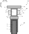
図1は、第1の実施形態の半導体装置の模式断面図である。 Figure 1 is a schematic cross-sectional view of a semiconductor device according to the first embodiment.
第1の実施形態の半導体装置は、トランジスタ100である。トランジスタ100は、酸化物半導体層にチャネルが形成される酸化物半導体トランジスタである。トランジスタ100は、チャネルが形成される酸化物半導体層の下側にゲート電極、上側にソース電極及びドレイン電極が設けられた、いわゆるボトムゲート型のトランジスタである。トランジスタ100は、電子をキャリアとするnチャネル型トランジスタである。
The semiconductor device of the first embodiment is a
トランジスタ100は、酸化物半導体層10、ゲート電極12、ゲート絶縁層14、ソース電極16、ドレイン電極18、バリア層20、コンタクト層22、第1の絶縁層24、及び第2の絶縁層26を備える。
The
ソース電極16は第1の電極の一例である。ドレイン電極18は第2の電極の一例である。バリア層20は第1の導電層の一例である。コンタクト層22は第2の導電層の一例である。
The
酸化物半導体層10には、トランジスタ100のオン動作時に、電流経路となるチャネルが形成される。チャネルの中で電子が流れる方向を、チャネル長方向と称する。図1中にチャネル長方向を両矢印で示す。
When the
酸化物半導体層10は、酸化物半導体である。酸化物半導体層10は、金属酸化物である。酸化物半導体層10は、例えば、アモルファスである。
The
酸化物半導体層10は、例えば、ガリウム(Ga)及びアルミニウム(Al)の少なくともいずれか一方の元素と、インジウム(In)と、亜鉛(Zn)とを含む。酸化物半導体層10の中に含まれる金属元素の原子濃度の総和に対する、インジウム、ガリウム、アルミニウム、及び亜鉛の原子濃度の総和の比は、例えば、90%以上である。また、酸化物半導体層10の中に含まれる酸素以外の元素の原子濃度の総和に対する、インジウム、ガリウム、アルミニウム、及び亜鉛の原子濃度の総和の比は、例えば、90%以上である。例えば、酸化物半導体層10の中には、酸素以外の元素で、インジウム、ガリウム、アルミニウム、及び亜鉛のいずれか一つよりも大きな原子濃度を有する元素は存在しない。
The
酸化物半導体層10に含まれる亜鉛(Zn)の原子濃度は、例えば、5原子%以上20原子%以下である。
The atomic concentration of zinc (Zn) contained in the
酸化物半導体層10は、第1の領域10a、第2の領域10b、及び第3の領域10cを有する。第3の領域10cは、第1の領域10aと第2の領域10bとの間の領域である。
The
酸化物半導体層10は、例えば、酸素欠損を含む。酸化物半導体層10の中の酸素欠損は、ドナーとして機能する。
The
酸化物半導体層10の厚さは、例えば、10nm以上100nm以下である。
The thickness of the
酸化物半導体層10は、例えば、原子層堆積法(Atomic Layer Deposition法:ALD法)により形成される。
The
ゲート電極12は、酸化物半導体層10の下側に設けられる。ゲート電極12は、例えば、金属、金属化合物、又は半導体である。ゲート電極12は、例えば、窒化チタン(TiN)又はタングステン(W)である。ゲート電極12のゲート長は、例えば、20nm以上100nm以下である。ゲート電極12のゲート長は、ゲート電極12のチャネル長方向の長さである。
The
ゲート絶縁層14は、酸化物半導体層10とゲート電極12との間に設けられる。ゲート絶縁層14は、第3の領域10cとゲート電極12との間に設けられる。
The
ゲート絶縁層14は、例えば、酸化物又は酸窒化物である。ゲート絶縁層14は、例えば、酸化シリコン又は酸化アルミニウムである。ゲート絶縁層14の厚さは、例えば、2nm以上10nm以下である。
The
なお、酸化物半導体層10とゲート絶縁層14との間に、ゲート絶縁層14と異なる材料の図示しない酸化物層を設けることも可能である。
It is also possible to provide an oxide layer (not shown) between the
ソース電極16は、酸化物半導体層10の上側に設けられる。酸化物半導体層10は、ゲート電極12とソース電極16との間に挟まれる。
The
ソース電極16は、第1の領域10aの上側に設けられる。ソース電極16は、第1の領域10aに電気的に接続される。
The
ソース電極16は、例えば、金属又は金属化合物である。ソース電極16は、例えば、バリア層20と異なる化学組成を有する金属である。
The
ソース電極16は、例えば、第2の金属元素を含む。例えば、ソース電極16に含まれる金属元素の原子濃度の中で、第2の金属元素の原子濃度が最も高い。
The source electrode 16 contains, for example, a second metal element. For example, among the atomic concentrations of the metal elements contained in the
第2の金属元素は、例えば、チタン(Ti)、タングステン(W)、銅(Cu)、アルミニウム(Al)、タンタル(Ta)、及びモリブデン(Mo)から成る群から選ばれる少なくとも一つの元素である。 The second metal element is, for example, at least one element selected from the group consisting of titanium (Ti), tungsten (W), copper (Cu), aluminum (Al), tantalum (Ta), and molybdenum (Mo).
ソース電極16は、例えば、チタン、窒化チタン、タングステン、窒化タングステン、銅、アルミニウム、タンタル、窒化タンタル、モリブデン、又は窒化モリブデンである。
The
ソース電極16に含まれる第2の金属元素は、例えば、バリア層20に含まれる第1の金属元素と同一である。また、ソース電極16に含まれる第2の金属元素は、例えば、バリア層20に含まれる第1の金属元素と異なる。
The second metal element contained in the
ソース電極16の厚さは、例えば、コンタクト層22の厚さよりも厚い。ソース電極16の厚さ及びコンタクト層22の厚さは、酸化物半導体層10からソース電極16へ向かう方向の厚さである。
The thickness of the
ドレイン電極18は、酸化物半導体層10の上側に設けられる。酸化物半導体層10は、ゲート電極12とドレイン電極18との間に挟まれる。
The
ドレイン電極18は、第2の領域10bの上側に設けられる。ドレイン電極18は、第2の領域10bに電気的に接続される。
The
ドレイン電極18は、例えば、第2の金属元素を含む。例えば、ドレイン電極18に含まれる金属元素の原子濃度の中で、第2の金属元素の原子濃度が最も高い。
The
第2の金属元素は、例えば、チタン(Ti)、タングステン(W)、銅(Cu)、アルミニウム(Al)、タンタル(Ta)、及びモリブデン(Mo)から成る群から選ばれる少なくとも一つの金属元素である。 The second metal element is, for example, at least one metal element selected from the group consisting of titanium (Ti), tungsten (W), copper (Cu), aluminum (Al), tantalum (Ta), and molybdenum (Mo).
ドレイン電極18は、例えば、チタン、窒化チタン、タングステン、窒化タングステン、銅、アルミニウム、タンタル、窒化タンタル、モリブデン、又は窒化モリブデンである。
The
ドレイン電極18に含まれる第2の金属元素は、例えば、バリア層20に含まれる第1の金属元素と同一である。また、ドレイン電極18に含まれる第2の金属元素は、例えば、バリア層20に含まれる第1の金属元素と異なる。
The second metal element contained in the
ドレイン電極18の厚さは、例えば、コンタクト層22の厚さよりも厚い。ドレイン電極18の厚さ及びコンタクト層22の厚さは、酸化物半導体層10からドレイン電極18へ向かう方向の厚さである。
The thickness of the
バリア層20は、酸化物半導体層10とソース電極16との間に設けられる。バリア層20は、第1の領域10aとソース電極16との間に設けられる。バリア層20は、例えば、ソース電極16に接する。バリア層20は、酸化物半導体層10からソース電極16側へ拡散する酸素の拡散バリアとして機能する。
The
バリア層20は、酸化物半導体層10とドレイン電極18との間に設けられる。バリア層20は、第2の領域10bとドレイン電極18との間に設けられる。バリア層20は、例えば、ドレイン電極18に接する。バリア層20は、酸化物半導体層10からドレイン電極18側へ拡散する酸素の拡散バリアとして機能する。
The
バリア層20は、第1の金属元素と、酸素(O)及び窒素(N)の少なくともいずれか一方の元素とを含む。例えば、バリア層20に含まれる、酸素(O)及び窒素(N)以外の元素の原子濃度の中で、第1の金属元素の原子濃度が最も高い。
The
第1の金属元素は、例えば、チタン(Ti)、タングステン(W)、銅(Cu)、アルミニウム(Al)、タンタル(Ta)、及びモリブデン(Mo)から成る群から選ばれる少なくとも一つの元素である The first metal element is, for example, at least one element selected from the group consisting of titanium (Ti), tungsten (W), copper (Cu), aluminum (Al), tantalum (Ta), and molybdenum (Mo).
バリア層20は、例えば、酸化物、窒化物、又は酸窒化物である。
The
バリア層20は、例えば、第1の金属元素としてチタン(Ti)を含む。バリア層20は、例えば、酸素(O)及び窒素(N)を含む。バリア層20は、例えば、酸化チタン又は酸窒化チタンである。
The
バリア層20の厚さは、例えば、コンタクト層22の厚さよりも薄い。バリア層20の厚さ及びコンタクト層22の厚さは、酸化物半導体層10からソース電極16へ向かう方向の厚さである。
The thickness of the
バリア層20の厚さは、例えば、コンタクト層22の厚さの2分の1以下である。バリア層20の厚さは、例えば、1nm以上10nm以下である。
The thickness of the
バリア層20は、例えば、結晶質である。バリア層20の結晶粒径は、例えば、コンタクト層22の結晶粒径よりも小さい。バリア層20及びコンタクト層22の結晶粒径は、例えば、結晶粒の長径の中央値で代表させる。
The
バリア層20は、例えば、アモルファスである。
The
バリア層20は、例えば、スパッタ法又はALD法により形成される。バリア層20は、例えば、ソース電極16又はドレイン電極18の一部を、酸化、窒化、又は酸窒化することにより形成される。
The
コンタクト層22は、酸化物半導体層10とバリア層20との間に設けられる。コンタクト層22は、第1の領域10aとソース電極16との間に設けられる。また、コンタクト層22は、第2の領域10bとドレイン電極18との間に設けられる。
The
コンタクト層22は、例えば、バリア層20に接する。コンタクト層22は、例えば、酸化物半導体層10に接する。コンタクト層22は、例えば、第1の領域10aに接する。コンタクト層22は、例えば、第2の領域10bに接する。
The
コンタクト層22は、第1の領域10aとソース電極16との間の電気抵抗を低減する機能を備える。コンタクト層22は、第2の領域10bとドレイン電極18との間の電気抵抗を低減する機能を備える。
The
コンタクト層22は、インジウム(In)、亜鉛(Zn)、スズ(Sn)、及びカドミウム(Cd)から成る群から選ばれる少なくとも一つの元素と、酸素(O)とを含む。コンタクト層22は、酸化物である。
The
コンタクト層22は、例えば、インジウム(In)及びスズ(Sn)を含む。コンタクト層22は、例えば、インジウム(In)及びスズ(Sn)を含む酸化物である。
The
コンタクト層22の厚さは、例えば、バリア層20の厚さよりも厚い。コンタクト層22の厚さ及びのバリア層20の厚さは、酸化物半導体層10からソース電極16へ向かう方向の厚さである。
The thickness of the
コンタクト層22の厚さは、例えば、バリア層20の厚さの2倍以上である。コンタクト層22の厚さは、例えば、5nm以上30nm以下である。
The thickness of the
コンタクト層22は、例えば、結晶質である。
The
コンタクト層22は、例えば、スパッタ法又はALD法により形成される。
The
第1の絶縁層24は、酸化物半導体層10の下側に設けられる。第1の絶縁層24は、例えば、酸化物、窒化物、又は酸窒化物である。第1の絶縁層24は、例えば、酸化シリコン、窒化シリコン、又は酸窒化シリコンである。
The first insulating
第2の絶縁層26は、酸化物半導体層10の上側に設けられる。第2の絶縁層26は、ソース電極16とドレイン電極18の間に設けられる。
The second insulating
第2の絶縁層26は、ソース電極16とドレイン電極18とを電気的に分離する。第2の絶縁層26は、例えば、酸化物、窒化物、又は酸窒化物である。第2の絶縁層26は、例えば、酸化シリコン、窒化シリコン、又は酸窒化シリコンである。
The second insulating
以下、第1の実施形態の半導体装置の作用及び効果について説明する。 The following describes the operation and effects of the semiconductor device of the first embodiment.
例えば、酸化物半導体トランジスタをメモリセルのスイッチングトランジスタに適用する場合、酸化物半導体トランジスタは、メモリセルや配線の形成に伴う熱処理を経ることになる。熱処理を経ることにより酸化物半導体トランジスタの閾値電圧の変動が生じる場合がある。 For example, when an oxide semiconductor transistor is used as a switching transistor of a memory cell, the oxide semiconductor transistor undergoes heat treatment associated with the formation of the memory cell and wiring. The heat treatment may cause the threshold voltage of the oxide semiconductor transistor to fluctuate.
酸化物半導体トランジスタの閾値電圧の変動は、チャネルが形成される酸化物半導体層の中の酸素が、ソース電極やドレイン電極の側に抜けることにより生ずる。酸化物半導体層の中の酸素が抜けることで、酸化物半導体層の中に酸素欠損が生じる。 The threshold voltage of an oxide semiconductor transistor fluctuates when oxygen in the oxide semiconductor layer where the channel is formed escapes to the source electrode or drain electrode side. When oxygen escapes from the oxide semiconductor layer, oxygen vacancies occur in the oxide semiconductor layer.
酸素欠損は、酸化物半導体層の中でドナーとして機能する。したがって、例えば、酸化物半導体トランジスタがnチャネル型トランジスタの場合、酸素欠損が生じると、酸化物半導体トランジスタの閾値電圧が低下する。 Oxygen vacancies function as donors in the oxide semiconductor layer. Therefore, for example, when the oxide semiconductor transistor is an n-channel transistor, the occurrence of oxygen vacancies reduces the threshold voltage of the oxide semiconductor transistor.
第1の実施形態のトランジスタ100は、酸化物半導体層10とソース電極16との間、及び、酸化物半導体層10とドレイン電極18との間に、酸素の拡散を抑制するバリア層20を備える。バリア層20を備えることで、酸化物半導体層10の中の酸素が、ソース電極16やドレイン電極18の側に抜けることが抑制される。したがって、トランジスタ100の閾値電圧の変動が抑制される。
The
酸素の拡散を抑制し、バリア層20の電気抵抗率を低減する観点から、バリア層20は、チタン(Ti)、タングステン(W)、銅(Cu)、アルミニウム(Al)、タンタル(Ta)、及びモリブデン(Mo)から成る群から選ばれる少なくとも一つの第1の金属元素と、酸素(O)及び窒素(N)の少なくともいずれか一方の元素と、を含むことが好ましい。バリア層20に含まれる、酸素(O)及び窒素(N)以外の元素の原子濃度の中で、第1の金属元素の原子濃度が最も高い。
From the viewpoint of suppressing oxygen diffusion and reducing the electrical resistivity of the
酸素の拡散を抑制し、バリア層20の電気抵抗率を低減する観点から、バリア層20は酸窒化チタンであることが好ましい。バリア層20は、チタン(Ti)、酸素(O)、及び窒素(N)を含むことが好ましい。第1の金属元素は、チタン(Ti)であることが好ましい。
From the viewpoint of suppressing oxygen diffusion and reducing the electrical resistivity of the
酸素の拡散を抑制する観点から、バリア層20の結晶粒径は小さいことが好ましい。酸素の拡散を抑制する観点から、バリア層20の結晶粒径は、コンタクト層22の結晶粒径よりも小さいことが好ましい。また、酸素の拡散を抑制する観点から、バリア層20はアモルファスであることが好ましい。
From the viewpoint of suppressing oxygen diffusion, it is preferable that the crystal grain size of the
バリア層20の厚さは、1nm以上10nm以下であることが好ましく、2nm以上8nm以下であることがより好ましい。上記下限値を上回ることにより、酸素の拡散抑制効果が向上する。上記上限値を下回ることにより、バリア層20の抵抗が低減し、ソース電極16と酸化物半導体層10との間の電気抵抗が低減できる。また、ドレイン電極18と酸化物半導体層10との間の電気抵抗が低減できる。
The thickness of the
第1の実施形態のトランジスタ100は、酸化物半導体層10とバリア層20との間に、コンタクト層22を備える。コンタクト層22を備えることにより、例えば、コンタクト層22を設けずバリア層20が直接に酸化物半導体層10に接する場合と比較して、コンタクト抵抗が低減する。
The
トランジスタ100のコンタクト層22は、インジウム(In)、亜鉛(Zn)、スズ(Sn)、及びカドミウム(Cd)から成る群から選ばれる少なくとも一つの元素と、酸素(O)とを含む酸化物である。コンタクト層22が、インジウム(In)、亜鉛(Zn)、スズ(Sn)、及びカドミウム(Cd)から成る群から選ばれる少なくとも一つの元素と、酸素(O)とを含む酸化物であることにより、酸化物半導体層10とコンタクト層22との間に、熱処理により高抵抗の反応生成物が形成されることが抑制できる。よって、酸化物半導体層10とコンタクト層22との間のコンタクト抵抗が低減できる。
The
酸化物半導体層10とコンタクト層22との間のコンタクト抵抗を低減する観点から、コンタクト層22は、インジウム(In)及びスズ(Sn)を含む酸化物であることが好ましい。
From the viewpoint of reducing the contact resistance between the
バリア層20の厚さは、コンタクト層22の厚さよりも薄いことが好ましい。バリア層20の厚さは、コンタクト層22の厚さの2分の1以下であることが好ましく、3分の1以下であることがより好ましい。
The thickness of the
コンタクト層22の厚さは、バリア層20の厚さよりも厚いことが好ましい。コンタクト層22の厚さは、バリア層20の厚さの2倍以上であることが好ましく、3倍以上であることがより好ましい。
The thickness of the
バリア層20の電気抵抗率は、コンタクト層22の電気抵抗率よりも高い。バリア層20の厚さを、コンタクト層22の厚さよりも薄くすること、言い換えれば、コンタクト層22の厚さをバリア層20の厚さよりも厚くすることにより、例えば、ソース電極16と酸化物半導体層10との間の電気抵抗が低減できる。また、ドレイン電極18と酸化物半導体層10との間の電気抵抗が低減できる。
The electrical resistivity of the
ソース電極16の厚さは、コンタクト層22の厚さよりも厚いことが好ましい。また、ドレイン電極18の厚さは、コンタクト層22の厚さよりも厚いことが好ましい。ソース電極16及びドレイン電極18の電気抵抗率は、コンタクト層22の電気抵抗率よりも低い。
The thickness of the
ソース電極16の厚さを、コンタクト層22の厚さよりも厚くすることにより、ソース電極16を配線として用いる場合の配線抵抗が低減できる。ドレイン電極18の厚さを、コンタクト層22の厚さよりも厚くすることにより、ドレイン電極18を配線として用いる場合の配線抵抗が低減できる。
By making the thickness of the
ソース電極16又はドレイン電極18は、耐熱性、抵抗、及び製造上の観点から、チタン(Ti)、タングステン(W)、銅(Cu)、アルミニウム(Al)、タンタル(Ta)、及びモリブデン(Mo)から成る群から選ばれる少なくとも一つの第2の金属元素を含むことが好ましい。ソース電極16又はドレイン電極18に含まれる金属元素の原子濃度の中で、第2の金属元素の原子濃度が最も高い。
From the viewpoints of heat resistance, resistance, and manufacturing, the
ソース電極16又はドレイン電極18は、耐熱性、抵抗、及び製造上の観点から、チタン(Ti)又はタングステン(W)を含むことがより好ましい。第2の金属元素は、チタン(Ti)又はタングステン(W)であることがより好ましい。ソース電極16又はドレイン電極18は、窒化チタン又はタングステンであることがより好ましい。
From the viewpoints of heat resistance, resistance, and manufacturing, it is more preferable that the
ソース電極16又はドレイン電極18に含まれる第2の金属元素は、バリア層20に含まれる第1の金属元素と同一であることが好ましい。ソース電極16又はドレイン電極18に含まれる第2の金属元素を、バリア層20に含まれる第1の金属元素と同一とすることで、ソース電極16又はドレイン電極18を、酸化、窒化、又は酸窒化することによりバリア層20を形成することが可能である。
The second metal element contained in the
ソース電極16又はドレイン電極18が窒化チタンであり、バリア層20が酸窒化チタンであることが好ましい。この場合、第1の金属元素及び第2の金属元素はチタン(Ti)である。この場合、ソース電極16又はドレイン電極18を酸化することにより、バリア層20を形成することが可能である。
It is preferable that the
ソース電極16又はドレイン電極18に含まれる第2の金属元素は、バリア層20に含まれる第1の金属元素と異なることが好ましい。ソース電極16又はドレイン電極18に含まれる第2の金属元素を、バリア層20に含まれる第1の金属元素と異なる金属元素とすることで、ソース電極16又はドレイン電極18とバリア層20を独立に形成することが可能である。
The second metal element contained in the
ソース電極16又はドレイン電極18がタングステンであり、バリア層20が酸窒化チタンであることが好ましい。この場合、第1の金属元素はチタン(Ti)、第2の金属元素はタングステン(W)である。
Preferably, the
以上、第1の実施形態によれば、熱処理後の閾値電圧の変動が抑制され、高い耐熱性を備えた酸化物半導体トランジスタが実現される。 As described above, according to the first embodiment, the variation in threshold voltage after heat treatment is suppressed, and an oxide semiconductor transistor with high heat resistance is realized.
(第2の実施形態)
第2の実施形態の半導体装置は、ゲート電極が、酸化物半導体層を囲む点で、第1の実施形態の半導体装置と異なっている。以下、第1の実施形態と重複する内容については、一部記述を省略する場合がある。
Second Embodiment
The semiconductor device of the second embodiment differs from the semiconductor device of the first embodiment in that the gate electrode surrounds the oxide semiconductor layer. In the following description, some of the contents that overlap with the first embodiment may be omitted.
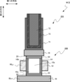
図2、図3は、第2の実施形態の半導体装置の模式断面図である。図3は、図2のAA’断面図である。図2において、水平方向を第1の方向、奥行方向を第2の方向、上下方向を第3の方向と称する。 Figures 2 and 3 are schematic cross-sectional views of a semiconductor device according to the second embodiment. Figure 3 is a cross-sectional view taken along line AA' in Figure 2. In Figure 2, the horizontal direction is referred to as the first direction, the depth direction as the second direction, and the up-down direction as the third direction.
第2の実施形態の半導体装置は、トランジスタ200である。トランジスタ200は、酸化物半導体にチャネルが形成される酸化物半導体トランジスタである。トランジスタ200は、ゲート電極が、チャネルが形成される酸化物半導体層を囲んで設けられる、いわゆるSurrounding Gate Transistor(SGT)である。トランジスタ200は、いわゆる縦型トランジスタである。
The semiconductor device of the second embodiment is a
トランジスタ200は、酸化物半導体層10、ゲート電極12、ゲート絶縁層14、ソース電極16、ドレイン電極18、バリア層20、コンタクト層22、層間絶縁層32を備える。ソース電極16は第1の電極の一例である。ドレイン電極18は第2の電極の一例である。バリア層20は第1の導電層の一例である。コンタクト層22は、第2の導電層の一例である。
The
酸化物半導体層10は、ソース電極16とドレイン電極18との間に設けられる。酸化物半導体層10には、トランジスタ200のオン動作時に、電流経路となるチャネルが形成される。酸化物半導体層10は、第3の方向に延びる。酸化物半導体層10は、第3の方向に延びる柱状である。酸化物半導体層10は、例えば、円柱状である。
The
チャネルの中で電子が流れる方向を、チャネル長方向と称する。第3の方向が、トランジスタ200のチャネル長方向である。
The direction in which electrons flow in the channel is called the channel length direction. The third direction is the channel length direction of
酸化物半導体層10は、酸化物半導体である。酸化物半導体層10は、金属酸化物である。酸化物半導体層10は、例えば、アモルファスである。
The
酸化物半導体層10は、例えば、ガリウム(Ga)及びアルミニウム(Al)の少なくともいずれか一方の元素と、インジウム(In)と、亜鉛(Zn)とを含む。酸化物半導体層10の中に含まれる金属元素の原子濃度の総和に対する、インジウム、ガリウム、アルミニウム、及び亜鉛の原子濃度の総和の比は、例えば、90%以上である。また、酸化物半導体層10の中に含まれる酸素以外の元素の原子濃度の総和に対する、インジウム、ガリウム、アルミニウム、及び亜鉛の原子濃度の総和の比は、例えば、90%以上である。例えば、酸化物半導体層10の中には、酸素以外の元素で、インジウム、ガリウム、アルミニウム、及び亜鉛のいずれか一つよりも大きな原子濃度を有する元素は存在しない。
The
酸化物半導体層10に含まれる亜鉛(Zn)の原子濃度は、例えば、5原子%以上20原子%以下である。
The atomic concentration of zinc (Zn) contained in the
酸化物半導体層10は、第1の領域10a、第2の領域10b、及び第3の領域10cを有する。第3の領域10cは、第1の領域10aと第2の領域10bとの間の領域である。
The
酸化物半導体層10は、例えば、酸素欠損を含む。酸化物半導体層10の中の酸素欠損は、ドナーとして機能する。
The
酸化物半導体層10の第1の方向の幅は、例えば、20nm以上100nm以下である。酸化物半導体層10の第3の方向の長さは、例えば、80nm以上200nm以下である。
The width of the
酸化物半導体層10は、例えば、ALD法により形成される。
The
ゲート電極12は、酸化物半導体層10を囲んで設けられる。ゲート電極12は、酸化物半導体層10の周囲に設けられる。
The
ゲート電極12は、例えば、金属、金属化合物、又は半導体である。ゲート電極12は、例えば、窒化チタン(TiN)又はタングステン(W)である。ゲート電極12のゲート長は、例えば、20nm以上100nm以下である。ゲート電極12のゲート長は、ゲート電極12の第3の方向の長さである。
The
ゲート絶縁層14は、酸化物半導体層10とゲート電極12との間に設けられる。ゲート絶縁層14は、酸化物半導体層10を囲んで設けられる。ゲート絶縁層14は、第3の領域10cとゲート電極12との間に設けられる。
The
ゲート絶縁層14は、例えば、酸化物又は酸窒化物である。ゲート絶縁層14は、例えば、酸化シリコン又は酸化アルミニウムである。ゲート絶縁層14の厚さは、例えば、2nm以上10nm以下である。
The
なお、酸化物半導体層10とゲート絶縁層14との間に、ゲート絶縁層14と異なる材料の図示しない酸化物層を設けることも可能である。
It is also possible to provide an oxide layer (not shown) between the
ソース電極16は、酸化物半導体層10の下側に設けられる。ソース電極16は、第1の領域10aの下側に設けられる。ソース電極16は、第1の領域10aに電気的に接続される。
The
ソース電極16は、例えば、金属又は金属化合物である。ソース電極16は、例えば、バリア層20と異なる化学組成を有する金属である。
The
ソース電極16は、例えば、第2の金属元素を含む。例えば、ソース電極16に含まれる金属元素の原子濃度の中で、第2の金属元素の原子濃度が最も高い。
The source electrode 16 contains, for example, a second metal element. For example, among the atomic concentrations of the metal elements contained in the
第2の金属元素は、例えば、チタン(Ti)、タングステン(W)、銅(Cu)、アルミニウム(Al)、タンタル(Ta)、及びモリブデン(Mo)から成る群から選ばれる少なくとも一つの元素である。 The second metal element is, for example, at least one element selected from the group consisting of titanium (Ti), tungsten (W), copper (Cu), aluminum (Al), tantalum (Ta), and molybdenum (Mo).
ソース電極16は、例えば、チタン、窒化チタン、タングステン、窒化タングステン、銅、アルミニウム、タンタル、窒化タンタル、モリブデン、又は窒化モリブデンである。
The
ソース電極16に含まれる第2の金属元素は、例えば、バリア層20に含まれる第1の金属元素と同一である。また、ソース電極16に含まれる第2の金属元素は、例えば、バリア層20に含まれる第1の金属元素と異なる。
The second metal element contained in the
ソース電極16の厚さは、例えば、コンタクト層22の厚さよりも厚い。ソース電極16の厚さ及びコンタクト層22の厚さは、酸化物半導体層10からソース電極16へ向かう方向の厚さである。
The thickness of the
ドレイン電極18は、酸化物半導体層10の上側に設けられる。ドレイン電極18は、第2の領域10bの上側に設けられる。ドレイン電極18は、第2の領域10bに電気的に接続される。
The
ドレイン電極18は、例えば、第2の金属元素を含む。例えば、ドレイン電極18に含まれる金属元素の原子濃度の中で、第2の金属元素の原子濃度が最も高い。
The
第2の金属元素は、例えば、チタン(Ti)、タングステン(W)、銅(Cu)、アルミニウム(Al)、タンタル(Ta)、及びモリブデン(Mo)から成る群から選ばれる少なくとも一つの金属元素である。 The second metal element is, for example, at least one metal element selected from the group consisting of titanium (Ti), tungsten (W), copper (Cu), aluminum (Al), tantalum (Ta), and molybdenum (Mo).
ドレイン電極18は、例えば、チタン、窒化チタン、タングステン、窒化タングステン、銅、アルミニウム、タンタル、窒化タンタル、モリブデン、又は窒化モリブデンである。
The
ドレイン電極18に含まれる第2の金属元素は、例えば、バリア層20に含まれる第1の金属元素と同一である。また、ドレイン電極18に含まれる第2の金属元素は、例えば、バリア層20に含まれる第1の金属元素と異なる。
The second metal element contained in the
ドレイン電極18の厚さは、例えば、コンタクト層22の厚さよりも厚い。ドレイン電極18の厚さ及びコンタクト層22の厚さは、酸化物半導体層10からドレイン電極18へ向かう方向の厚さである。
The thickness of the
バリア層20は、酸化物半導体層10とソース電極16との間に設けられる。バリア層20は、第1の領域10aとソース電極16との間に設けられる。バリア層20は、例えば、ソース電極16に接する。バリア層20は、酸化物半導体層10からソース電極16側へ拡散する酸素の拡散バリアとして機能する。
The
バリア層20は、酸化物半導体層10とドレイン電極18との間に設けられる。バリア層20は、第2の領域10bとドレイン電極18との間に設けられる。バリア層20は、例えば、ドレイン電極18に接する。バリア層20は、酸化物半導体層10からドレイン電極18側へ拡散する酸素の拡散バリアとして機能する。
The
バリア層20は、第1の金属元素と、酸素(O)及び窒素(N)の少なくともいずれか一方の元素とを含む。例えば、バリア層20に含まれる、酸素(O)及び窒素(N)以外の元素の原子濃度の中で、第1の金属元素の原子濃度が最も高い。
The
第1の金属元素は、例えば、チタン(Ti)、タングステン(W)、銅(Cu)、アルミニウム(Al)、タンタル(Ta)、及びモリブデン(Mo)から成る群から選ばれる少なくとも一つの元素である The first metal element is, for example, at least one element selected from the group consisting of titanium (Ti), tungsten (W), copper (Cu), aluminum (Al), tantalum (Ta), and molybdenum (Mo).
バリア層20は、例えば、酸化物、窒化物、又は酸窒化物である。
The
バリア層20は、例えば、第1の金属元素としてチタン(Ti)を含む。バリア層20は、例えば、酸素(O)及び窒素(N)を含む。バリア層20は、例えば、酸化チタン又は酸窒化チタンである。
The
バリア層20の厚さは、例えば、コンタクト層22の厚さよりも薄い。バリア層20の厚さ及びコンタクト層22の厚さは、酸化物半導体層10からソース電極16へ向かう方向の厚さである。
The thickness of the
バリア層20の厚さは、例えば、コンタクト層22の厚さの2分の1以下である。バリア層20の厚さは、例えば、1nm以上10nm以下である。
The thickness of the
バリア層20は、例えば、結晶質である。バリア層20の結晶粒径は、例えば、コンタクト層22の結晶粒径よりも小さい。バリア層20及びコンタクト層22の結晶粒径は、例えば、結晶粒の長径の中央値で代表させる。
The
バリア層20は、例えば、アモルファスである。
The
コンタクト層22は、酸化物半導体層10とバリア層20との間に設けられる。コンタクト層22は、第1の領域10aとソース電極16との間に設けられる。また、コンタクト層22は、第2の領域10bとドレイン電極18との間に設けられる。
The
コンタクト層22は、例えば、バリア層20に接する。コンタクト層22は、例えば、酸化物半導体層10に接する。コンタクト層22は、例えば、第1の領域10aに接する。コンタクト層22は、例えば、第2の領域10bに接する。
The
コンタクト層22は、第1の領域10aとソース電極16との間の抵抗を低減する機能を備える。コンタクト層22は、第2の領域10bとドレイン電極18との間の抵抗を低減する機能を備える。
The
コンタクト層22は、インジウム(In)、亜鉛(Zn)、スズ(Sn)、及びカドミウム(Cd)から成る群から選ばれる少なくとも一つの元素と、酸素(O)とを含む。コンタクト層22は、酸化物である。
The
コンタクト層22は、例えば、インジウム(In)及びスズ(Sn)を含む。コンタクト層22は、例えば、インジウム(In)及びスズ(Sn)を含む酸化物である。
The
コンタクト層22の厚さは、例えば、バリア層20の厚さよりも厚い。コンタクト層22の厚さ及びのバリア層20の厚さは、酸化物半導体層10からソース電極16へ向かう方向の厚さである。
The thickness of the
コンタクト層22の厚さは、例えば、バリア層20の厚さの2倍以上である。コンタクト層22の厚さは、例えば、5nm以上30nm以下である。
The thickness of the
コンタクト層22は、例えば、結晶質である。
The
コンタクト層22は、例えば、スパッタ法又はALD法により形成される。
The
層間絶縁層32は、ゲート電極12、ソース電極16、及びドレイン電極18の周囲に設けられる。層間絶縁層32は、例えば、酸化物、窒化物、又は酸窒化物である。層間絶縁層32は、例えば、酸化シリコン、窒化シリコン、又は酸窒化シリコンである。
The interlayer insulating
以上、第2の実施形態によれば、第1の実施形態と同様、熱処理後の閾値電圧の変動が抑制され、高い耐熱性を備えた酸化物半導体トランジスタが実現される。また、第2の実施形態によれば、SGTであることにより、単位面積あたりに高い密度でトランジスタを配置することが可能となる。 As described above, according to the second embodiment, as in the first embodiment, the variation in threshold voltage after heat treatment is suppressed, and an oxide semiconductor transistor with high heat resistance is realized. Furthermore, according to the second embodiment, since the transistor is an SGT, it is possible to arrange transistors at a high density per unit area.
(第3の実施形態)
第1の方向に延びる第1の配線と、第1の方向と交差する第2の方向に延びる第2の配線と、メモリセルと、を備え、メモリセルは、第1の領域と、第2の領域と、第1の領域と第2の領域との間の第3の領域と、を含み、第1の領域が第1の配線に電気的に接続され、第3の領域が第2の配線の一部に囲まれた酸化物半導体層と、第3の領域と第2の配線の一部との間に設けられたゲート絶縁層と、第2の領域に電気的に接続された第1の電極と、第2の電極と、第1の電極と第2の電極との間の絶縁層と、を含むキャパシタと、第1の領域と第1の配線との間、及び、第2の領域と第1の電極との間の少なくとも一方の位置に設けられ、酸素(O)及び窒素(N)の少なくともいずれか一方の元素と、第1の金属元素と、を含む第1の導電層と、酸化物半導体層と第1の導電層との間に設けられ、インジウム(In)、亜鉛(Zn)、スズ(Sn)、及びカドミウム(Cd)から成る群から選ばれる少なくとも一つの元素と、酸素(O)と、を含む第2の導電層と、を備える。以下、第1又は第2の実施形態と重複する内容については、一部記述を省略する場合がある。
Third Embodiment
The memory cell includes a first wiring extending in a first direction, a second wiring extending in a second direction intersecting the first direction, and a memory cell, the memory cell including a first region, a second region, and a third region between the first region and the second region, the first region being electrically connected to the first wiring, an oxide semiconductor layer in which the third region is surrounded by a part of the second wiring, a gate insulating layer provided between the third region and a part of the second wiring, a first electrode electrically connected to the second region, a second electrode, and a gate insulating layer between the first electrode and the second electrode. and an insulating layer between the first region and the first wiring, a first conductive layer provided at least at one of positions between the second region and the first electrode and containing at least one element of oxygen (O) and nitrogen (N) and a first metal element, and a second conductive layer provided between the oxide semiconductor layer and the first conductive layer and containing at least one element selected from the group consisting of indium (In), zinc (Zn), tin (Sn), and cadmium (Cd) and oxygen (O). Hereinafter, some of the contents that overlap with the first or second embodiment may be omitted.
第3の実施形態の半導体記憶装置は、半導体メモリ300である。第3の実施形態の半導体記憶装置は、Dynamic Random Access Memory(DRAM)である。半導体メモリ300は、第2の実施形態のトランジスタ200を、DRAMのメモリセルのスイッチングトランジスタとして使用する。
The semiconductor memory device of the third embodiment is a
図4は、第3の実施形態の半導体記憶装置のブロック図である。 Figure 4 is a block diagram of a semiconductor memory device according to the third embodiment.
図4に示すように、半導体メモリ300は、メモリセルアレイ210、ワード線ドライバ回路212、ローデコーダ回路214、センスアンプ回路215、カラムデコーダ回路217、及び制御回路221を備える。
As shown in FIG. 4, the
図5、図6は、第3の実施形態の半導体記憶装置のメモリセルアレイの模式断面図である。図5は、第1の方向と第3の方向を含む面の断面図、図6は、第2の方向と第3の方向を含む面の断面図である。第1の方向と第2の方向は交差する。第1の方向と第2の方向は、例えば垂直である。第3の方向は、第1の方向及び第2の方向に対して垂直な方向である。第3の方向は、例えば基板に対して垂直な方向である。 Figures 5 and 6 are schematic cross-sectional views of a memory cell array of a semiconductor memory device of the third embodiment. Figure 5 is a cross-sectional view of a plane including a first direction and a third direction, and Figure 6 is a cross-sectional view of a plane including a second direction and a third direction. The first direction and the second direction intersect. The first direction and the second direction are, for example, perpendicular. The third direction is a direction perpendicular to the first direction and the second direction. The third direction is, for example, a direction perpendicular to the substrate.
第3の実施形態のメモリセルアレイ210は、メモリセルが立体的に配置された三次元構造を備える。図5、図6において破線で囲まれた領域がそれぞれ1個のメモリセルを表している。
The
メモリセルアレイ210は、シリコン基板250を備える。
The
メモリセルアレイ210は、シリコン基板250の上に、例えば、複数のビット線BLと複数のワード線WLを備える。ビット線BLは第1の方向に伸長する。ワード線WLは第2の方向に伸長する。
The
ビット線BLとワード線WLとは、例えば、垂直に交差する。ビット線BLとワード線WLとの交差する領域に、メモリセルが配置される。メモリセルには、第1のメモリセルMC1及び第2のメモリセルMC2が含まれる。第1のメモリセルMC1及び第2のメモリセルMC2は、メモリセルの一例である。 The bit line BL and the word line WL intersect, for example, perpendicularly. Memory cells are arranged in the areas where the bit line BL and the word line WL intersect. The memory cells include a first memory cell MC1 and a second memory cell MC2. The first memory cell MC1 and the second memory cell MC2 are examples of memory cells.
第1のメモリセルMC1及び第2のメモリセルMC2に接続されるビット線BLがビット線BLxである。ビット線BLxは、第1の配線の一例である。第1のメモリセルMC1に接続されるワード線WLがワード線WLxである。ワード線WLxは、第2の配線の一例である。 The bit line BL connected to the first memory cell MC1 and the second memory cell MC2 is the bit line BLx. The bit line BLx is an example of a first wiring. The word line WL connected to the first memory cell MC1 is the word line WLx. The word line WLx is an example of a second wiring.
第2のメモリセルMC2に接続されるワード線WLがワード線WLyである。ワード線WLxは、ビット線BLxの一方の側に設けられる。ワード線WLyは、ビット線BLxの他方の側に設けられる。 The word line WL connected to the second memory cell MC2 is the word line WLy. The word line WLx is provided on one side of the bit line BLx. The word line WLy is provided on the other side of the bit line BLx.
メモリセルアレイ210は、複数のプレート電極線PLを有する。プレート電極線PLは各メモリセルのプレート電極72に接続される。
The
メモリセルアレイ210は、各配線及び各電極の電気的分離のために層間絶縁層260を備える。
The
複数のワード線WLは、ローデコーダ回路214に電気的に接続される。複数のビット線BLは、センスアンプ回路215に電気的に接続される。
The word lines WL are electrically connected to a
ローデコーダ回路214は、入力されたローアドレス信号に従ってワード線WLを選択する機能を備える。ワード線ドライバ回路212は、ローデコーダ回路214によって選択されたワード線WLに所定の電圧を印加する機能を備える。
The
カラムデコーダ回路217は、入力されたカラムアドレス信号に従ってビット線BLを選択する機能を備える。センスアンプ回路215は、カラムデコーダ回路217によって選択されたビット線BLに所定の電圧を印加する機能を備える。また、ビット線BLの電位を検知して増幅する機能を備える。
The
制御回路221は、ワード線ドライバ回路212、ローデコーダ回路214、センスアンプ回路215、カラムデコーダ回路217、及び、図示しないその他の回路を制御する機能を備える。
The
ワード線ドライバ回路212、ローデコーダ回路214、センスアンプ回路215、カラムデコーダ回路217、及び制御回路221などの回路は、例えば、図示しないトランジスタや配線層によって構成される。トランジスタは、例えば、シリコン基板250を用いて形成される。
Circuits such as the word
ビット線BL及びワード線WLは、例えば金属である。ビット線BL及びワード線WLは、例えば、窒化チタン、タングステン、又は窒化チタンとタングステンの積層構造である。 The bit line BL and the word line WL are, for example, metal. The bit line BL and the word line WL are, for example, titanium nitride, tungsten, or a layered structure of titanium nitride and tungsten.
図7は、第3の実施形態の半導体記憶装置の第1のメモリセルの模式断面図である。図8は、第3の実施形態の半導体記憶装置の第2のメモリセルの模式断面図である。 Figure 7 is a schematic cross-sectional view of a first memory cell of a semiconductor memory device of the third embodiment. Figure 8 is a schematic cross-sectional view of a second memory cell of a semiconductor memory device of the third embodiment.
第1のメモリセルMC1は、シリコン基板250とビット線BLxとの間に設けられる。シリコン基板250と第2のメモリセルMC2との間に、ビット線BLxが設けられる。 The first memory cell MC1 is provided between the silicon substrate 250 and the bit line BLx. The bit line BLx is provided between the silicon substrate 250 and the second memory cell MC2.
第1のメモリセルMC1は、ビット線BLxの下側に設けられる。第2のメモリセルMC2は、ビット線BLxの上側に設けられる。 The first memory cell MC1 is provided below the bit line BLx. The second memory cell MC2 is provided above the bit line BLx.
第1のメモリセルMC1は、ビット線BLxの一方の側に設けられる。第2のメモリセルMC2は、ビット線BLxの他方の側に設けられる。 The first memory cell MC1 is provided on one side of the bit line BLx. The second memory cell MC2 is provided on the other side of the bit line BLx.
第2のメモリセルMC2は、第1のメモリセルMC1を上下反転させた構造を有する。第1のメモリセルMC1及び第2のメモリセルMC2は、それぞれトランジスタ200及びキャパシタ201を備える。
The second memory cell MC2 has a structure in which the first memory cell MC1 is inverted upside down. The first memory cell MC1 and the second memory cell MC2 each include a
トランジスタ200は、酸化物半導体層10、ゲート電極12、ゲート絶縁層14、ソース電極16、ドレイン電極18、バリア層20、及びコンタクト層22を備える。バリア層20は第1の導電層の一例である。コンタクト層22は第2の導電層の一例である。トランジスタ200は、第2の実施形態のトランジスタ200と同様の構成を備える。
The
酸化物半導体層10は、第1の領域10a、第2の領域10b、及び第3の領域10cを有する。第3の領域10cは、第1の領域10aと第2の領域10bとの間の領域である。
The
キャパシタ201は、セル電極71、プレート電極72、キャパシタ絶縁膜73を備える。セル電極71及びプレート電極72は、例えば、窒化チタンである。また、キャパシタ絶縁膜73は、例えば、酸化ジルコニウム、酸化アルミニウム、酸化ジルコニウムの積層構造を有する。
The
セル電極71は、第1の電極の一例である。プレート電極72は、第2の電極の一例である。キャパシタ絶縁膜73は、絶縁層の一例である。
The
キャパシタ201は、第1のメモリセルMC1及び第2のメモリセルMC2の酸化物半導体層10の一端に電気的に接続される。キャパシタ201のセル電極71は、ドレイン電極18に接続される。プレート電極72はプレート電極線PLに接続される。ドレイン電極18は、セル電極71の一部とみなすことができる。
The
ソース電極16はビット線BLに接続される。ゲート電極12はワード線WLに接続される。ソース電極16はビット線BLの一部とみなすことができる。
The
なお、図5、図6、図7、図8では、ビット線BLとソース電極16、及び、ワード線WLとゲート電極12は、同一の材料で同時形成される場合を例に示している。ビット線BLとソース電極16、及び、ワード線WLとゲート電極12は、それぞれ異なる材料で別々に形成されるものであっても構わない。
Note that in Figures 5, 6, 7, and 8, the bit line BL and
ビット線BLxは、例えば、第2の金属元素を含む。例えば、ビット線BLxに含まれる金属元素の原子濃度の中で、第2の金属元素の原子濃度が最も高い。 The bit line BLx includes, for example, a second metal element. For example, among the atomic concentrations of the metal elements included in the bit line BLx, the atomic concentration of the second metal element is the highest.
第2の金属元素は、例えば、チタン(Ti)、タングステン(W)、銅(Cu)、アルミニウム(Al)、タンタル(Ta)、及びモリブデン(Mo)から成る群から選ばれる少なくとも一つの元素である。 The second metal element is, for example, at least one element selected from the group consisting of titanium (Ti), tungsten (W), copper (Cu), aluminum (Al), tantalum (Ta), and molybdenum (Mo).
ビット線BLxは、例えば、チタン、窒化チタン、タングステン、窒化タングステン、銅、アルミニウム、タンタル、窒化タンタル、モリブデン、又は窒化モリブデンである。 The bit line BLx is, for example, titanium, titanium nitride, tungsten, tungsten nitride, copper, aluminum, tantalum, tantalum nitride, molybdenum, or molybdenum nitride.
ビット線BLxに含まれる第2の金属元素は、例えば、バリア層20に含まれる第1の金属元素と同一である。また、ビット線BLxに含まれる第2の金属元素は、例えば、バリア層20に含まれる第1の金属元素と異なる。
The second metal element contained in the bit line BLx is, for example, the same as the first metal element contained in the
セル電極71は、例えば、第2の金属元素を含む。例えば、セル電極71に含まれる金属元素の原子濃度の中で、第2の金属元素の原子濃度が最も高い。
The
第2の金属元素は、例えば、チタン(Ti)、タングステン(W)、銅(Cu)、アルミニウム(Al)、タンタル(Ta)、及びモリブデン(Mo)から成る群から選ばれる少なくとも一つの金属元素である。 The second metal element is, for example, at least one metal element selected from the group consisting of titanium (Ti), tungsten (W), copper (Cu), aluminum (Al), tantalum (Ta), and molybdenum (Mo).
セル電極71は、例えば、チタン、窒化チタン、タングステン、窒化タングステン、銅、アルミニウム、タンタル、窒化タンタル、モリブデン、又は窒化モリブデンである。
The
セル電極71に含まれる第2の金属元素は、例えば、バリア層20に含まれる第1の金属元素と同一である。また、ドレイン電極18に含まれる第2の金属元素は、例えば、バリア層20に含まれる第1の金属元素と異なる。
The second metal element contained in the
第1のメモリセルMC1の酸化物半導体層10のキャパシタ201が接続される端部と反対側の端部(他端)に、ビット線BLxが電気的に接続される。第2のメモリセルMC2の酸化物半導体層10のキャパシタ201が接続される端部と反対側の端部(他端)にビット線BLxが電気的に接続される。
The bit line BLx is electrically connected to the end (other end) of the
第1のメモリセルMC1のゲート電極12にワード線WLxが電気的に接続される。また、第2のメモリセルMC2のゲート電極12にワード線WLyが電気的に接続される。
A word line WLx is electrically connected to the
トランジスタ200は、酸化物半導体層10とソース電極16及びドレイン電極18との間にバリア層20を備える。また、酸化物半導体層10とバリア層20との間に、コンタクト層22を備える。
The
酸化物半導体トランジスタをDRAMのメモリセルのスイッチングトランジスタとして使用する場合、トランジスタ形成後に高温かつ長時間の熱処理が加えられる。熱処理は、例えば、キャパシタ形成のための熱処理である。高温かつ長時間の熱処理により、酸化物半導体トランジスタの閾値電圧の変動が生じやすい。 When an oxide semiconductor transistor is used as a switching transistor for a DRAM memory cell, a high-temperature, long-term heat treatment is performed after the transistor is formed. The heat treatment is, for example, heat treatment for forming a capacitor. High-temperature, long-term heat treatment is likely to cause fluctuations in the threshold voltage of the oxide semiconductor transistor.
トランジスタ200は、酸化物半導体層10とソース電極16及びドレイン電極18との間にバリア層20を備える。したがって、トランジスタ形成後に高温かつ長時間の熱処理が加えられても、閾値電圧の変動が抑制される。
The
また、トランジスタ200は、酸化物半導体層10とバリア層20との間に、コンタクト層22を備える。したがって、コンタクト抵抗が低減する。よって、トランジスタ200のオン電流が増加する。
The
ビット線BLxの厚さは、コンタクト層22の厚さよりも厚いことが好ましい。ビット線BLxの厚さ及びコンタクト層22の厚さは、第3の方向の厚さである。
The thickness of the bit line BLx is preferably thicker than the thickness of the
ビット線BLxの電気抵抗率は、コンタクト層22の電気抵抗率よりも低い。ビット線BLxの厚さを、コンタクト層22の厚さよりも厚くすることにより、ビット線BLxの配線抵抗を低減できる。
The electrical resistivity of the bit line BLx is lower than that of the
セル電極71の厚さは、コンタクト層22の厚さよりも厚いことが好ましい。セル電極71の厚さ及びコンタクト層22の厚さは、第3の方向の厚さである。
The thickness of the
第3の実施形態によれば、第2の実施形態のトランジスタ200をDRAMのスイッチングトランジスタとして用いることにより、熱処理後の閾値電圧の変動が抑制され、高い耐熱性を備えた半導体メモリが実現される。
According to the third embodiment, by using the
(第4の実施形態)
第4の実施形態の半導体装置は、酸化物半導体層と、電極と、酸化物半導体層と電極との間に設けられ、第1の金属元素と、を含む第1の導電層と、酸素(O)及び窒素(N)の少なくともいずれか一方の元素と、酸化物半導体層と第1の導電層との間に設けられ、インジウム(In)、亜鉛(Zn)、スズ(Sn)、及びカドミウム(Cd)から成る群から選ばれる少なくとも一つの元素と、酸素(O)と、を含む第2の導電層と、を備える。以下、第1の実施形態と重複する内容については、一部記述を省略する場合がある。
(Fourth embodiment)
The semiconductor device of the fourth embodiment includes an oxide semiconductor layer, an electrode, a first conductive layer provided between the oxide semiconductor layer and the electrode and containing a first metal element, and a second conductive layer provided between the oxide semiconductor layer and the first conductive layer and containing at least one element selected from the group consisting of indium (In), zinc (Zn), tin (Sn), and cadmium (Cd), and oxygen (O). Hereinafter, some of the contents that overlap with the first embodiment may be omitted.
図9は、第4の実施形態の半導体装置の模式断面図である。 Figure 9 is a schematic cross-sectional view of a semiconductor device according to the fourth embodiment.
第4の実施形態の半導体装置は、コンタクト構造400を含む。コンタクト構造400は、酸化物半導体層10、バリア層20、コンタクト層22、配線層40、コンタクトプラグ42、層間絶縁層44を備える。バリア層20は第1の導電層の一例である。コンタクト層22は、第2の導電層の一例である。コンタクトプラグ42は電極の一例である。
The semiconductor device of the fourth embodiment includes a
酸化物半導体層10は、酸化物半導体である。酸化物半導体層10は、金属酸化物である。酸化物半導体層10は、例えば、アモルファスである。
The
酸化物半導体層10は、例えば、ガリウム(Ga)及びアルミニウム(Al)の少なくともいずれか一方の元素と、インジウム(In)と、亜鉛(Zn)とを含む。酸化物半導体層10の中に含まれる金属元素の原子濃度の総和に対する、インジウム、ガリウム、アルミニウム、及び亜鉛の原子濃度の総和の比は、例えば、90%以上である。また、酸化物半導体層10の中に含まれる酸素以外の元素の原子濃度の総和に対する、インジウム、ガリウム、アルミニウム、及び亜鉛の原子濃度の総和の比は、例えば、90%以上である。例えば、酸化物半導体層10の中には、酸素以外の元素で、インジウム、ガリウム、アルミニウム、及び亜鉛のいずれか一つよりも大きな原子濃度を有する元素は存在しない。
The
配線層40は、例えば、金属又は金属化合物である。
The
コンタクトプラグ42は、酸化物半導体層10と配線層40との間に設けられる。
The
コンタクトプラグ42は、例えば、金属又は金属化合物である。コンタクトプラグ42は、例えば、バリア層20と異なる化学組成を有する金属である。
The
コンタクトプラグ42は、例えば、第2の金属元素を含む。例えば、コンタクトプラグ42に含まれる金属元素の原子濃度の中で、第2の金属元素の原子濃度が最も高い。
The contact plug 42 contains, for example, a second metal element. For example, the atomic concentration of the second metal element is the highest among the atomic concentrations of the metal elements contained in the
第2の金属元素は、例えば、チタン(Ti)、タングステン(W)、銅(Cu)、アルミニウム(Al)、タンタル(Ta)、及びモリブデン(Mo)から成る群から選ばれる少なくとも一つの元素である。 The second metal element is, for example, at least one element selected from the group consisting of titanium (Ti), tungsten (W), copper (Cu), aluminum (Al), tantalum (Ta), and molybdenum (Mo).
コンタクトプラグ42は、例えば、チタン、窒化チタン、タングステン、窒化タングステン、銅、アルミニウム、タンタル、窒化タンタル、モリブデン、又は窒化モリブデンである。
The
コンタクトプラグ42に含まれる第2の金属元素は、例えば、バリア層20に含まれる第1の金属元素と同一である。また、コンタクトプラグ42に含まれる第2の金属元素は、例えば、バリア層20に含まれる第1の金属元素と異なる。
The second metal element contained in the
コンタクトプラグ42の厚さは、例えば、コンタクトプラグ42の厚さよりも厚い。コンタクトプラグ42の厚さ及びコンタクト層22の厚さは、酸化物半導体層10からコンタクトプラグ42へ向かう方向の厚さである。
The thickness of the
バリア層20は、酸化物半導体層10とコンタクトプラグ42との間に設けられる。バリア層20は、例えば、コンタクトプラグ42に接する。バリア層20は、酸化物半導体層10からコンタクトプラグ42側へ拡散する酸素の拡散バリアとして機能する。
The
バリア層20は、第1の金属元素と、酸素(O)及び窒素(N)の少なくともいずれか一方の元素とを含む。例えば、バリア層20に含まれる、酸素(O)及び窒素(N)以外の元素の原子濃度の中で、第1の金属元素の原子濃度が最も高い。
The
第1の金属元素は、例えば、チタン(Ti)、タングステン(W)、銅(Cu)、アルミニウム(Al)、タンタル(Ta)、及びモリブデン(Mo)から成る群から選ばれる少なくとも一つの金属元素である The first metal element is, for example, at least one metal element selected from the group consisting of titanium (Ti), tungsten (W), copper (Cu), aluminum (Al), tantalum (Ta), and molybdenum (Mo).
バリア層20は、例えば、酸化物、窒化物、又は酸窒化物である。
The
バリア層20は、例えば、第1の金属元素としてチタン(Ti)を含む。バリア層20は、例えば、酸素(O)及び窒素(N)を含む。バリア層20は、酸化チタン又は酸窒化チタンである。
The
バリア層20の厚さは、例えば、コンタクト層22の厚さよりも薄い。バリア層20の厚さ及びコンタクト層22の厚さは、酸化物半導体層10からコンタクトプラグ42へ向かう方向の厚さである。
The thickness of the
バリア層20の厚さは、例えば、コンタクト層22の厚さの2分の1以下である。バリア層20の厚さは、例えば、1nm以上10nm以下である。
The thickness of the
バリア層20は、例えば、結晶質である。バリア層20の結晶粒径は、例えば、コンタクト層22の結晶粒径よりも小さい。バリア層20及びコンタクト層22の結晶粒径は、例えば、結晶粒の長径の中央値で代表させる。
The
バリア層20は、例えば、アモルファスである。
The
バリア層20は、例えば、スパッタ法又はALD法により形成される。バリア層20は、例えば、コンタクトプラグ42の一部を、酸化、窒化、又は酸窒化することにより形成される。
The
コンタクト層22は、酸化物半導体層10とバリア層20との間に設けられる。コンタクト層22は、例えば、バリア層20に接する。コンタクト層22は、例えば、酸化物半導体層10に接する。
The
コンタクト層22は、酸化物半導体層10とコンタクトプラグ42との間の電気抵抗を低減する機能を備える。
The
コンタクト層22は、インジウム(In)、亜鉛(Zn)、スズ(Sn)、及びカドミウム(Cd)から成る群から選ばれる少なくとも一つの元素と、酸素(O)とを含む。コンタクト層22は、酸化物である。
The
コンタクト層22は、例えば、インジウム(In)及びスズ(Sn)を含む。コンタクト層22は、例えば、インジウム(In)及びスズ(Sn)を含む酸化物である。
The
コンタクト層22の厚さは、例えば、バリア層20の厚さよりも厚い。コンタクト層22の厚さ及びバリア層20の厚さは、酸化物半導体層10からコンタクトプラグ42へ向かう方向の厚さである。
The thickness of the
コンタクト層22の厚さは、例えば、バリア層20の厚さの2倍以上である。コンタクト層22の厚さは、例えば、5nm以上30nm以下である。
The thickness of the
コンタクト層22は、例えば、結晶質である。
The
コンタクト層22は、例えば、スパッタ法又はALD法により形成される。
The
層間絶縁層44は、酸化物半導体層10と配線層40との間に設けられる。層間絶縁層44は、例えば、酸化シリコン、窒化シリコン、又は酸窒化シリコンである。
The interlayer insulating
コンタクト構造400が、バリア層20を備えない場合、コンタクト構造400を形成した後に加わる熱処理により酸化物半導体層の中の酸素が、コンタクトプラグ42の側に抜ける。酸化物半導体層の中の酸素が抜けることで、酸化物半導体層の中に酸素欠損が生じる。酸素欠損は、酸化物半導体層の中でドナーとして機能する。
If the
コンタクトプラグ42の下の酸化物半導体層10の中のドナーの濃度が変化すると、酸化物半導体層10とコンタクトプラグ42との間のコンタクト抵抗が変動する。酸化物半導体層10とコンタクトプラグ42との間のコンタクト抵抗が不安定になる。
When the donor concentration in the
コンタクト構造400は、酸化物半導体層10とコンタクトプラグ42との間にバリア層20を備える。バリア層20を備えることにより、酸化物半導体層10の中のドナーの濃度の変化が抑制される。したがって、酸化物半導体層10とコンタクトプラグ42との間のコンタクト抵抗が安定する。
The
また、コンタクト構造400は、酸化物半導体層10とバリア層20との間に、コンタクト層22を備える。したがって、酸化物半導体層10とコンタクトプラグ42との間のコンタクト抵抗が低減する。
The
以上、第4の実施形態によれば、熱処理後のコンタクト抵抗の変動が抑制され、高い耐熱性を備えた半導体装置が実現される。 As described above, according to the fourth embodiment, the fluctuation of the contact resistance after heat treatment is suppressed, and a semiconductor device with high heat resistance is realized.
第1ないし第4の実施形態では、第1の領域10aとソース電極16との間、及び、第2の領域10bとドレイン電極18との間の両方の位置に、バリア層20及びコンタクト層22が設けられるトランジスタを例に説明した。しかし、バリア層20及びコンタクト層22が、第1の領域10aとソース電極16との間、及び、第2の領域10bとドレイン電極18との間の、いずれか一方の位置のみに設けられるトランジスタとすることも可能である。
In the first to fourth embodiments, a transistor in which the
第1ないし第4の実施形態では、酸化物半導体層10が、ガリウム(Ga)及びアルミニウム(Al)の少なくともいずれか一方の元素と、インジウム(In)と、亜鉛(Zn)とを含む金属酸化物である場合を例に説明したが、酸化物半導体層10にその他の金属酸化物を適用することも可能である。
In the first to fourth embodiments, the
以上、本発明のいくつかの実施形態を説明したが、これらの実施形態は、例として提示したものであり、発明の範囲を限定することは意図していない。これら新規な実施形態は、その他の様々な形態で実施されることが可能であり、発明の要旨を逸脱しない範囲で、種々の省略、置き換え、変更を行うことができる。例えば、一実施形態の構成要素を他の実施形態の構成要素と置き換え又は変更してもよい。これら実施形態やその変形は、発明の範囲や要旨に含まれるとともに、特許請求の範囲に記載された発明とその均等の範囲に含まれる。 Although several embodiments of the present invention have been described above, these embodiments are presented as examples and are not intended to limit the scope of the invention. These novel embodiments can be implemented in various other forms, and various omissions, substitutions, and modifications can be made without departing from the gist of the invention. For example, components of one embodiment may be replaced or modified with components of another embodiment. These embodiments and their modifications are included within the scope and gist of the invention, and are included in the scope of the invention and its equivalents as set forth in the claims.
10 酸化物半導体層
10a 第1の領域
10b 第2の領域
10c 第3の領域
12 ゲート電極
14 ゲート絶縁層
16 ソース電極(第1の電極)
18 ドレイン電極(第2の電極)
20 バリア層(第1の導電層)
22 コンタクト層(第2の導電層)
71 セル電極(第1の電極)
72 プレート電極(第2の電極)
73 キャパシタ絶縁膜(絶縁層)
100 トランジスタ(半導体装置)
200 トランジスタ(半導体装置)
201 キャパシタ
300 半導体メモリ(半導体記憶装置)
BLx ビット線(第1の配線)
MC1 第1のメモリセル(メモリセル)
WLx ワード線(第2の配線)
10
18 Drain electrode (second electrode)
20 Barrier layer (first conductive layer)
22 Contact layer (second conductive layer)
71 Cell electrode (first electrode)
72 Plate electrode (second electrode)
73 Capacitor insulating film (insulating layer)
100 Transistor (semiconductor device)
200 Transistor (semiconductor device)
BLx bit line (first wiring)
MC1 First memory cell (memory cell)
WLx Word line (second wiring)
Claims (19)
ゲート電極と、
前記第3の領域と前記ゲート電極との間に設けられたゲート絶縁層と、
前記第1の領域に電気的に接続された第1の電極と、
前記第2の領域に電気的に接続された第2の電極と、
前記第1の領域と前記第1の電極との間、及び、前記第2の領域と前記第2の電極との間の少なくとも一方の位置に設けられ、酸素(O)と、窒素(N)と、第1の金属元素と、を含む第1の導電層と、
前記酸化物半導体層と前記第1の導電層との間に設けられ、インジウム(In)、亜鉛(Zn)、スズ(Sn)、及びカドミウム(Cd)から成る群から選ばれる少なくとも一つの元素と、酸素(O)と、を含み、厚さが前記第1の導電層の厚さよりも厚い第2の導電層と、
を備え、
前記第1の金属元素はチタン(Ti)である半導体装置。 an oxide semiconductor layer including a first region, a second region, and a third region between the first region and the second region;
A gate electrode;
a gate insulating layer provided between the third region and the gate electrode;
a first electrode electrically connected to the first region;
a second electrode electrically connected to the second region;
a first conductive layer provided at least one of a position between the first region and the first electrode and a position between the second region and the second electrode, the first conductive layer including oxygen (O), nitrogen (N) and a first metal element;
a second conductive layer provided between the oxide semiconductor layer and the first conductive layer, containing at least one element selected from the group consisting of indium (In), zinc (Zn), tin (Sn), and cadmium (Cd) and oxygen (O), and having a thickness greater than that of the first conductive layer;
Equipped with
The semiconductor device , wherein the first metal element is titanium (Ti) .
前記少なくともいずれか一方の電極に含まれる金属元素の原子濃度の中で、前記第2の金属元素の原子濃度が最も高く、
前記第2の金属元素は前記第1の金属元素と同一である請求項1ないし請求項4いずれか一項記載の半導体装置。 at least one of the first electrode having the first conductive layer provided between it and the oxide semiconductor layer and the second electrode having the first conductive layer provided between it and the oxide semiconductor layer contains a second metal element;
the atomic concentration of the second metal element is the highest among the atomic concentrations of the metal elements contained in the at least one of the electrodes;
5. The semiconductor device according to claim 1 , wherein the second metal element is the same as the first metal element.
前記少なくともいずれか一方の電極に含まれる金属元素の原子濃度の中で、前記第2の金属元素の原子濃度が最も高く、
前記第2の金属元素は前記第1の金属元素と異なる請求項1ないし請求項4いずれか一項記載の半導体装置。 at least one of the first electrode having the first conductive layer provided between it and the oxide semiconductor layer and the second electrode having the first conductive layer provided between it and the oxide semiconductor layer contains a second metal element;
the atomic concentration of the second metal element is the highest among the atomic concentrations of the metal elements contained in the at least one of the electrodes;
5. The semiconductor device according to claim 1 , wherein the second metal element is different from the first metal element.
ゲート電極と、
前記第3の領域と前記ゲート電極との間に設けられたゲート絶縁層と、
前記第1の領域に電気的に接続された第1の電極と、
前記第2の領域に電気的に接続された第2の電極と、
前記第1の領域と前記第1の電極との間、及び、前記第2の領域と前記第2の電極との間の少なくとも一方の位置に設けられた第1の導電層であって、チタン(Ti)、タングステン(W)、銅(Cu)、アルミニウム(Al)、タンタル(Ta)、及びモリブデン(Mo)から成る群から選ばれる少なくとも一つの第1の金属元素と、酸素(O)と、窒素(N)と、を含み、前記第1の導電層の中に含まれる酸素(O)及び窒素(N)以外の元素の原子濃度の中で、前記第1の金属元素の原子濃度が最も高い第1の導電層と、
前記酸化物半導体層と前記第1の導電層との間に設けられ、インジウム(In)、亜鉛(Zn)、スズ(Sn)、及びカドミウム(Cd)から成る群から選ばれる少なくとも一つの元素と、酸素(O)と、を含む第2の導電層と、
を備え、
前記第1の金属元素はチタン(Ti)である半導体装置。 an oxide semiconductor layer including a first region, a second region, and a third region between the first region and the second region;
A gate electrode;
a gate insulating layer provided between the third region and the gate electrode;
a first electrode electrically connected to the first region;
a second electrode electrically connected to the second region;
a first conductive layer provided at least at one of the positions between the first region and the first electrode and between the second region and the second electrode, the first conductive layer including at least one first metal element selected from the group consisting of titanium (Ti), tungsten (W), copper (Cu), aluminum (Al), tantalum (Ta), and molybdenum (Mo), oxygen (O), and nitrogen (N) , and the atomic concentration of the first metal element is the highest among atomic concentrations of elements other than oxygen (O) and nitrogen (N) contained in the first conductive layer;
a second conductive layer provided between the oxide semiconductor layer and the first conductive layer, the second conductive layer containing at least one element selected from the group consisting of indium (In), zinc (Zn), tin (Sn), and cadmium (Cd) and oxygen (O);
Equipped with
The semiconductor device , wherein the first metal element is titanium (Ti) .
ゲート電極と、
前記第3の領域と前記ゲート電極との間に設けられたゲート絶縁層と、
前記第1の領域に電気的に接続された第1の電極と、
前記第2の領域に電気的に接続された第2の電極と、
前記第1の領域と前記第1の電極との間、及び、前記第2の領域と前記第2の電極との間の少なくとも一方の位置に設けられ、酸素(O)と、窒素(N)と、第1の金属元素と、を含む第1の導電層と、
前記酸化物半導体層と前記第1の導電層との間に設けられ、インジウム(In)、亜鉛(Zn)、スズ(Sn)、及びカドミウム(Cd)から成る群から選ばれる少なくとも一つの元素と、酸素(O)と、を含む第2の導電層と、を備え、
前記酸化物半導体層との間に前記第1の導電層が設けられた前記第1の電極、又は、前記酸化物半導体層との間に前記第1の導電層が設けられた前記第2の電極、の少なくともいずれか一方の電極は、第2の金属元素を含み、
前記少なくともいずれか一方の電極に含まれる金属元素の原子濃度の中で、前記第2の金属元素の原子濃度が最も高く、
前記第2の金属元素は前記第1の金属元素と同一であり、
前記第1の金属元素はチタン(Ti)である半導体装置。 an oxide semiconductor layer including a first region, a second region, and a third region between the first region and the second region;
A gate electrode;
a gate insulating layer provided between the third region and the gate electrode;
a first electrode electrically connected to the first region;
a second electrode electrically connected to the second region;
a first conductive layer provided at least one of a position between the first region and the first electrode and a position between the second region and the second electrode, the first conductive layer including oxygen (O), nitrogen (N) and a first metal element;
a second conductive layer provided between the oxide semiconductor layer and the first conductive layer, the second conductive layer containing at least one element selected from the group consisting of indium (In), zinc (Zn), tin (Sn), and cadmium (Cd) and oxygen (O);
at least one of the first electrode having the first conductive layer provided between it and the oxide semiconductor layer and the second electrode having the first conductive layer provided between it and the oxide semiconductor layer contains a second metal element;
the atomic concentration of the second metal element is the highest among the atomic concentrations of the metal elements contained in the at least one of the electrodes;
the second metal element is the same as the first metal element;
The semiconductor device , wherein the first metal element is titanium (Ti) .
前記第1の方向と交差する第2の方向に延びる第2の配線と、
メモリセルと、を備え、
前記メモリセルは、
第1の領域と、第2の領域と、前記第1の領域と前記第2の領域との間の第3の領域と、を含み、前記第1の領域が前記第1の配線に電気的に接続され、前記第3の領域が前記第2の配線の一部に囲まれた酸化物半導体層と、
前記第3の領域と前記第2の配線の一部との間に設けられたゲート絶縁層と、
前記第2の領域に電気的に接続された第1の電極と、第2の電極と、前記第1の電極と前記第2の電極との間の絶縁層と、を含むキャパシタと、
前記第1の領域と前記第1の配線との間、及び、前記第2の領域と前記第1の電極との間の少なくとも一方の位置に設けられ、酸素(O)と、窒素(N)と、第1の金属元素と、を含む第1の導電層と、
前記酸化物半導体層と前記第1の導電層との間に設けられ、インジウム(In)、亜鉛(Zn)、スズ(Sn)、及びカドミウム(Cd)から成る群から選ばれる少なくとも一つの元素と、酸素(O)と、を含み、厚さが前記第1の導電層の厚さよりも厚い第2の導電層と、
を備え、
前記第1の金属元素はチタン(Ti)である半導体記憶装置。 A first wiring extending in a first direction;
a second wiring extending in a second direction intersecting the first direction;
A memory cell,
The memory cell includes:
an oxide semiconductor layer including a first region, a second region, and a third region between the first region and the second region, the first region being electrically connected to the first wiring, and the third region being surrounded by a part of the second wiring;
a gate insulating layer provided between the third region and a portion of the second wiring;
a capacitor including a first electrode electrically connected to the second region, a second electrode, and an insulating layer between the first electrode and the second electrode;
a first conductive layer provided at least one of a position between the first region and the first wiring and a position between the second region and the first electrode, the first conductive layer including oxygen (O), nitrogen (N) and a first metal element;
a second conductive layer provided between the oxide semiconductor layer and the first conductive layer, containing at least one element selected from the group consisting of indium (In), zinc (Zn), tin (Sn), and cadmium (Cd) and oxygen (O), and having a thickness greater than that of the first conductive layer;
Equipped with
The first metal element is titanium (Ti) .
前記少なくともいずれか一方に含まれる金属元素の原子濃度の中で、前記第2の金属元素の原子濃度が最も高く、
前記第2の金属元素は前記第1の金属元素と同一である請求項11ないし請求項14いずれか一項記載の半導体記憶装置。 at least one of the first wiring having the first conductive layer provided between it and the oxide semiconductor layer and the first electrode having the first conductive layer provided between it and the oxide semiconductor layer contains a second metal element;
Among the atomic concentrations of metal elements contained in at least one of the first and second metal elements, the atomic concentration of the second metal element is the highest,
15. The semiconductor memory device according to claim 11, wherein the second metal element is the same as the first metal element.
前記少なくともいずれか一方に含まれる金属元素の原子濃度の中で、前記第2の金属元素の原子濃度が最も高く、
前記第2の金属元素は前記第1の金属元素と異なる請求項11ないし請求項14いずれか一項記載の半導体記憶装置。 at least one of the first wiring having the first conductive layer provided between it and the oxide semiconductor layer and the first electrode having the first conductive layer provided between it and the oxide semiconductor layer contains a second metal element;
Among the atomic concentrations of metal elements contained in at least one of the first and second metal elements, the atomic concentration of the second metal element is the highest,
15. The semiconductor memory device according to claim 11, wherein the second metal element is different from the first metal element.
前記第1の方向と交差する第2の方向に延びる第2の配線と、
メモリセルと、を備え、
前記メモリセルは、
第1の領域と、第2の領域と、前記第1の領域と前記第2の領域との間の第3の領域と、を含み、前記第1の領域が前記第1の配線に電気的に接続され、前記第3の領域が前記第2の配線の一部に囲まれた酸化物半導体層と、
前記第3の領域と前記第2の配線の一部との間に設けられたゲート絶縁層と、
前記第2の領域に電気的に接続されたキャパシタと、
前記第1の領域と前記第1の配線との間、及び、前記第2の領域と前記キャパシタとの間の少なくとも一方の位置に設けられた第1の導電層であって、チタン(Ti)、タングステン(W)、銅(Cu)、アルミニウム(Al)、タンタル(Ta)、及びモリブデン(Mo)から成る群から選ばれる少なくとも一つの第1の金属元素と、酸素(O)と、窒素(N)と、を含み、前記第1の導電層の中に含まれる酸素(O)及び窒素(N)以外の元素の原子濃度の中で、前記第1の金属元素の原子濃度が最も高い第1の導電層と、
前記酸化物半導体層と前記第1の導電層との間に設けられ、インジウム(In)、亜鉛(Zn)、スズ(Sn)、及びカドミウム(Cd)から成る群から選ばれる少なくとも一つの元素と、酸素(O)と、を含む第2の導電層と、
を備え、
前記第1の金属元素はチタン(Ti)である半導体記憶装置。 A first wiring extending in a first direction;
a second wiring extending in a second direction intersecting the first direction;
A memory cell,
The memory cell includes:
an oxide semiconductor layer including a first region, a second region, and a third region between the first region and the second region, the first region being electrically connected to the first wiring, and the third region being surrounded by a part of the second wiring;
a gate insulating layer provided between the third region and a portion of the second wiring;
a capacitor electrically connected to the second region;
a first conductive layer provided at least at one of a position between the first region and the first wiring and a position between the second region and the capacitor, the first conductive layer including at least one first metal element selected from a group consisting of titanium (Ti), tungsten (W), copper (Cu), aluminum (Al), tantalum (Ta), and molybdenum (Mo), oxygen (O), and nitrogen (N), and the atomic concentration of the first metal element is the highest among atomic concentrations of elements other than oxygen (O) and nitrogen (N ) contained in the first conductive layer;
a second conductive layer provided between the oxide semiconductor layer and the first conductive layer, the second conductive layer containing at least one element selected from the group consisting of indium (In), zinc (Zn), tin (Sn), and cadmium (Cd) and oxygen (O);
Equipped with
The first metal element is titanium (Ti) .
前記第1の方向と交差する第2の方向に延びる第2の配線と、
メモリセルと、を備え、
前記メモリセルは、
第1の領域と、第2の領域と、前記第1の領域と前記第2の領域との間の第3の領域と、を含み、前記第1の領域が前記第1の配線に電気的に接続され、前記第3の領域が前記第2の配線の一部に囲まれた酸化物半導体層と、
前記第3の領域と前記第2の配線の一部との間に設けられたゲート絶縁層と、
前記第2の領域に電気的に接続された第1の電極と、第2の電極と、前記第1の電極と前記第2の電極との間の絶縁層と、を含むキャパシタと、
前記第1の領域と前記第1の配線との間、及び、前記第2の領域と前記第1の電極との間の少なくとも一方の位置に設けられた第1の導電層であって、酸素(O)と、窒素(N)と、第1の金属元素と、を含む第1の導電層と、
前記酸化物半導体層と前記第1の導電層との間に設けられ、インジウム(In)、亜鉛(Zn)、スズ(Sn)、及びカドミウム(Cd)から成る群から選ばれる少なくとも一つの元素と、酸素(O)と、を含む第2の導電層と、を備え、
前記酸化物半導体層との間に前記第1の導電層が設けられた前記第1の配線、又は、前記酸化物半導体層との間に前記第1の導電層が設けられた前記第1の電極、の少なくともいずれか一方は、第2の金属元素を含み、
前記少なくともいずれか一方に含まれる金属元素の原子濃度の中で、前記第2の金属元素の原子濃度が最も高く、
前記第2の金属元素は前記第1の金属元素と同一であり、
前記第1の金属元素はチタン(Ti)である半導体記憶装置。 A first wiring extending in a first direction;
a second wiring extending in a second direction intersecting the first direction;
A memory cell,
The memory cell includes:
an oxide semiconductor layer including a first region, a second region, and a third region between the first region and the second region, the first region being electrically connected to the first wiring, and the third region being surrounded by a part of the second wiring;
a gate insulating layer provided between the third region and a portion of the second wiring;
a capacitor including a first electrode electrically connected to the second region, a second electrode, and an insulating layer between the first electrode and the second electrode;
a first conductive layer provided at least one of a position between the first region and the first wiring and a position between the second region and the first electrode, the first conductive layer including oxygen (O), nitrogen (N) and a first metal element;
a second conductive layer provided between the oxide semiconductor layer and the first conductive layer, the second conductive layer containing at least one element selected from the group consisting of indium (In), zinc (Zn), tin (Sn), and cadmium (Cd) and oxygen (O);
at least one of the first wiring having the first conductive layer provided between it and the oxide semiconductor layer and the first electrode having the first conductive layer provided between it and the oxide semiconductor layer contains a second metal element;
Among the atomic concentrations of metal elements contained in at least one of the first and second metal elements, the atomic concentration of the second metal element is the highest,
the second metal element is the same as the first metal element;
The first metal element is titanium (Ti) .
Priority Applications (4)
| Application Number | Priority Date | Filing Date | Title |
|---|---|---|---|
| JP2021047614A JP7612472B2 (en) | 2021-03-22 | 2021-03-22 | Semiconductor device and semiconductor memory device |
| TW110120640A TWI797636B (en) | 2021-03-22 | 2021-06-07 | Semiconductor device and semiconductor memory device |
| CN202110702228.5A CN115117062A (en) | 2021-03-22 | 2021-06-24 | Semiconductor device and semiconductor memory device |
| US17/470,871 US12089395B2 (en) | 2021-03-22 | 2021-09-09 | Semiconductor device and semiconductor memory device |
Applications Claiming Priority (1)
| Application Number | Priority Date | Filing Date | Title |
|---|---|---|---|
| JP2021047614A JP7612472B2 (en) | 2021-03-22 | 2021-03-22 | Semiconductor device and semiconductor memory device |
Publications (2)
| Publication Number | Publication Date |
|---|---|
| JP2022146576A JP2022146576A (en) | 2022-10-05 |
| JP7612472B2 true JP7612472B2 (en) | 2025-01-14 |
Family
ID=83284238
Family Applications (1)
| Application Number | Title | Priority Date | Filing Date |
|---|---|---|---|
| JP2021047614A Active JP7612472B2 (en) | 2021-03-22 | 2021-03-22 | Semiconductor device and semiconductor memory device |
Country Status (4)
| Country | Link |
|---|---|
| US (1) | US12089395B2 (en) |
| JP (1) | JP7612472B2 (en) |
| CN (1) | CN115117062A (en) |
| TW (1) | TWI797636B (en) |
Families Citing this family (6)
| Publication number | Priority date | Publication date | Assignee | Title |
|---|---|---|---|---|
| JP7612472B2 (en) * | 2021-03-22 | 2025-01-14 | キオクシア株式会社 | Semiconductor device and semiconductor memory device |
| KR102710108B1 (en) * | 2021-09-24 | 2024-09-25 | 한국전자통신연구원 | SRAM device including oxide semiconductor |
| JP2024000648A (en) | 2022-06-21 | 2024-01-09 | キオクシア株式会社 | Semiconductor devices and semiconductor storage devices |
| JP2024137422A (en) * | 2023-03-24 | 2024-10-07 | キオクシア株式会社 | Semiconductor device and semiconductor memory device |
| CN121533154A (en) * | 2023-08-10 | 2026-02-13 | 株式会社半导体能源研究所 | Semiconductor device with a semiconductor device having a plurality of semiconductor chips |
| KR20250113219A (en) * | 2024-01-18 | 2025-07-25 | 삼성전자주식회사 | Semiconductor device and method of manufacturing the same |
Citations (6)
| Publication number | Priority date | Publication date | Assignee | Title |
|---|---|---|---|---|
| JP2007173796A (en) | 2005-12-19 | 2007-07-05 | Internatl Business Mach Corp <Ibm> | Semiconductor structure using metal oxynitride as pFET material and manufacturing method thereof |
| JP2010056539A (en) | 2008-07-31 | 2010-03-11 | Semiconductor Energy Lab Co Ltd | Semiconductor device and manufacturing method thereof |
| WO2012002573A1 (en) | 2010-07-02 | 2012-01-05 | 合同会社先端配線材料研究所 | Semiconductor device |
| WO2012002574A1 (en) | 2010-07-02 | 2012-01-05 | 合同会社先端配線材料研究所 | Thin film transistor |
| JP2020003798A (en) | 2009-09-04 | 2020-01-09 | 株式会社半導体エネルギー研究所 | Display device |
| JP2020198343A (en) | 2019-05-31 | 2020-12-10 | キオクシア株式会社 | Semiconductor device and semiconductor memory device |
Family Cites Families (26)
| Publication number | Priority date | Publication date | Assignee | Title |
|---|---|---|---|---|
| KR100861236B1 (en) * | 2007-04-10 | 2008-10-02 | 경북대학교 산학협력단 | Low Leakage Current Column Effect Transistor |
| JP5579848B2 (en) | 2010-06-21 | 2014-08-27 | 株式会社アルバック | Semiconductor device, liquid crystal display device having semiconductor device, and method of manufacturing semiconductor device |
| JP5731369B2 (en) * | 2010-12-28 | 2015-06-10 | 株式会社半導体エネルギー研究所 | Method for manufacturing semiconductor device |
| KR20130048703A (en) | 2011-11-02 | 2013-05-10 | 히타치 덴센 가부시키가이샤 | Thin film transistor, manufacturing method therefor, and display apparatus having thin film transistor, sputtering target material |
| KR101925012B1 (en) * | 2012-07-17 | 2018-12-05 | 에스케이하이닉스 주식회사 | Semiconductor device and method for manufacturing the same |
| CN102931091A (en) * | 2012-10-25 | 2013-02-13 | 深圳市华星光电技术有限公司 | Driving matrix type flat panel display device, thin film transistor and manufacturing method of driving matrix type flat panel display device and thin film transistor |
| JP2014143410A (en) | 2012-12-28 | 2014-08-07 | Semiconductor Energy Lab Co Ltd | Semiconductor device and manufacturing method of the same |
| KR102290801B1 (en) | 2013-06-21 | 2021-08-17 | 가부시키가이샤 한도오따이 에네루기 켄큐쇼 | Semiconductor device and manufacturing method thereof |
| JP6347704B2 (en) * | 2013-09-18 | 2018-06-27 | 株式会社半導体エネルギー研究所 | Semiconductor device |
| US9177875B2 (en) * | 2013-11-15 | 2015-11-03 | Taiwan Seminconductor Manufacturing Co., Ltd. | Advanced process control method for controlling width of spacer and dummy sidewall in semiconductor device |
| TWI532192B (en) * | 2014-02-20 | 2016-05-01 | 友達光電股份有限公司 | Thin film transistor and pixel structure |
| KR20170080320A (en) | 2015-12-31 | 2017-07-10 | 엘지디스플레이 주식회사 | Thin film transistor, display with the same, and method of fabricating the same |
| JP6538598B2 (en) | 2016-03-16 | 2019-07-03 | 株式会社東芝 | Transistor and semiconductor memory device |
| US10157926B2 (en) * | 2016-08-31 | 2018-12-18 | Micron Technology, Inc. | Memory cells and memory arrays |
| US10644123B2 (en) * | 2016-09-30 | 2020-05-05 | Intel Corporation | Systems, methods, and apparatuses for implementing a high mobility low contact resistance semiconducting oxide in metal contact vias for thin film transistors |
| EP3559997A4 (en) * | 2016-12-24 | 2020-11-04 | INTEL Corporation | VERTICAL TRANSISTOR DEVICES AND METHODS |
| WO2018118097A1 (en) * | 2016-12-24 | 2018-06-28 | Intel Corporation | Vertical transistor devices and techniques |
| WO2019005090A1 (en) * | 2017-06-30 | 2019-01-03 | Intel Corporation | Semiconducting oxide device source and drain contacts including graded indium layers |
| WO2019046630A1 (en) * | 2017-08-31 | 2019-03-07 | Micron Technology, Inc. | Semiconductor devices, transistors, and related methods for contacting metal oxide semiconductor devices |
| JP7109928B2 (en) | 2018-01-31 | 2022-08-01 | キオクシア株式会社 | TRANSISTOR, SEMICONDUCTOR MEMORY DEVICE, AND TRANSISTOR MANUFACTURING METHOD |
| US20200006570A1 (en) * | 2018-06-29 | 2020-01-02 | Intel Corporation | Contact structures for thin film transistor devices |
| US11444205B2 (en) * | 2018-09-26 | 2022-09-13 | Intel Corporatiion | Contact stacks to reduce hydrogen in thin film transistor |
| JP2021108331A (en) * | 2019-12-27 | 2021-07-29 | キオクシア株式会社 | Semiconductor storage device |
| US11488981B2 (en) * | 2020-07-21 | 2022-11-01 | Micron Technology, Inc. | Array of vertical transistors and method used in forming an array of vertical transistors |
| JP2022049605A (en) * | 2020-09-16 | 2022-03-29 | キオクシア株式会社 | Semiconductor device and semiconductor storage device |
| JP7612472B2 (en) * | 2021-03-22 | 2025-01-14 | キオクシア株式会社 | Semiconductor device and semiconductor memory device |
-
2021
- 2021-03-22 JP JP2021047614A patent/JP7612472B2/en active Active
- 2021-06-07 TW TW110120640A patent/TWI797636B/en active
- 2021-06-24 CN CN202110702228.5A patent/CN115117062A/en active Pending
- 2021-09-09 US US17/470,871 patent/US12089395B2/en active Active
Patent Citations (6)
| Publication number | Priority date | Publication date | Assignee | Title |
|---|---|---|---|---|
| JP2007173796A (en) | 2005-12-19 | 2007-07-05 | Internatl Business Mach Corp <Ibm> | Semiconductor structure using metal oxynitride as pFET material and manufacturing method thereof |
| JP2010056539A (en) | 2008-07-31 | 2010-03-11 | Semiconductor Energy Lab Co Ltd | Semiconductor device and manufacturing method thereof |
| JP2020003798A (en) | 2009-09-04 | 2020-01-09 | 株式会社半導体エネルギー研究所 | Display device |
| WO2012002573A1 (en) | 2010-07-02 | 2012-01-05 | 合同会社先端配線材料研究所 | Semiconductor device |
| WO2012002574A1 (en) | 2010-07-02 | 2012-01-05 | 合同会社先端配線材料研究所 | Thin film transistor |
| JP2020198343A (en) | 2019-05-31 | 2020-12-10 | キオクシア株式会社 | Semiconductor device and semiconductor memory device |
Also Published As
| Publication number | Publication date |
|---|---|
| JP2022146576A (en) | 2022-10-05 |
| TWI797636B (en) | 2023-04-01 |
| US12089395B2 (en) | 2024-09-10 |
| CN115117062A (en) | 2022-09-27 |
| TW202238855A (en) | 2022-10-01 |
| US20220302120A1 (en) | 2022-09-22 |
Similar Documents
| Publication | Publication Date | Title |
|---|---|---|
| TWI786507B (en) | Semiconductor device and semiconductor memory device | |
| JP7612472B2 (en) | Semiconductor device and semiconductor memory device | |
| US11769810B2 (en) | Semiconductor device and semiconductor memory device | |
| US20200381557A1 (en) | Semiconductor device and semiconductor memory device | |
| US11502204B2 (en) | Semiconductor device and semiconductor memory device | |
| US11374130B2 (en) | Semiconductor device and semiconductor memory device | |
| US11978806B2 (en) | Semiconductor device and semiconductor storage device | |
| US20260047068A1 (en) | Semiconductor device and semiconductor memory device | |
| TWI872299B (en) | Semiconductor device and semiconductor memory device | |
| JP2023136275A (en) | Semiconductor device and semiconductor storage device | |
| TWI852037B (en) | Semiconductor device, semiconductor memory device, and method for manufacturing semiconductor device | |
| US12310065B2 (en) | Semiconductor device, semiconductor memory device, and method for manufacturing semiconductor device | |
| US12520527B2 (en) | Semiconductor device and semiconductor memory device |
Legal Events
| Date | Code | Title | Description |
|---|---|---|---|
| A621 | Written request for application examination |
Free format text: JAPANESE INTERMEDIATE CODE: A621 Effective date: 20230907 |
|
| A977 | Report on retrieval |
Free format text: JAPANESE INTERMEDIATE CODE: A971007 Effective date: 20240516 |
|
| A131 | Notification of reasons for refusal |
Free format text: JAPANESE INTERMEDIATE CODE: A131 Effective date: 20240625 |
|
| A521 | Request for written amendment filed |
Free format text: JAPANESE INTERMEDIATE CODE: A523 Effective date: 20240806 |
|
| TRDD | Decision of grant or rejection written | ||
| A01 | Written decision to grant a patent or to grant a registration (utility model) |
Free format text: JAPANESE INTERMEDIATE CODE: A01 Effective date: 20241126 |
|
| A61 | First payment of annual fees (during grant procedure) |
Free format text: JAPANESE INTERMEDIATE CODE: A61 Effective date: 20241225 |
|
| R150 | Certificate of patent or registration of utility model |
Ref document number: 7612472 Country of ref document: JP Free format text: JAPANESE INTERMEDIATE CODE: R150 |