JP7611209B2 - 統合された磁気を備える高速ネットワークコネクタ - Google Patents
統合された磁気を備える高速ネットワークコネクタ Download PDFInfo
- Publication number
- JP7611209B2 JP7611209B2 JP2022174513A JP2022174513A JP7611209B2 JP 7611209 B2 JP7611209 B2 JP 7611209B2 JP 2022174513 A JP2022174513 A JP 2022174513A JP 2022174513 A JP2022174513 A JP 2022174513A JP 7611209 B2 JP7611209 B2 JP 7611209B2
- Authority
- JP
- Japan
- Prior art keywords
- core body
- contacts
- connector
- circuit board
- printed circuit
- Prior art date
- Legal status (The legal status is an assumption and is not a legal conclusion. Google has not performed a legal analysis and makes no representation as to the accuracy of the status listed.)
- Active
Links
- 230000005291 magnetic effect Effects 0.000 title claims description 86
- 238000002955 isolation Methods 0.000 claims description 67
- 230000013011 mating Effects 0.000 claims description 62
- 230000008878 coupling Effects 0.000 claims description 20
- 238000010168 coupling process Methods 0.000 claims description 20
- 238000005859 coupling reaction Methods 0.000 claims description 20
- 238000000034 method Methods 0.000 claims description 16
- 238000004519 manufacturing process Methods 0.000 claims description 7
- 239000011347 resin Substances 0.000 claims description 4
- 229920005989 resin Polymers 0.000 claims description 4
- 239000004593 Epoxy Substances 0.000 claims description 3
- 238000004804 winding Methods 0.000 claims description 2
- 230000008901 benefit Effects 0.000 description 7
- 230000005540 biological transmission Effects 0.000 description 7
- 238000013461 design Methods 0.000 description 5
- 239000003989 dielectric material Substances 0.000 description 5
- 239000004020 conductor Substances 0.000 description 4
- 238000004891 communication Methods 0.000 description 2
- 230000001419 dependent effect Effects 0.000 description 2
- 238000010586 diagram Methods 0.000 description 2
- 238000009413 insulation Methods 0.000 description 2
- 230000000295 complement effect Effects 0.000 description 1
- 238000012938 design process Methods 0.000 description 1
- 230000000694 effects Effects 0.000 description 1
- 238000005516 engineering process Methods 0.000 description 1
- 239000003302 ferromagnetic material Substances 0.000 description 1
- 238000003780 insertion Methods 0.000 description 1
- 230000037431 insertion Effects 0.000 description 1
- 239000002184 metal Substances 0.000 description 1
- 238000012986 modification Methods 0.000 description 1
- 230000004048 modification Effects 0.000 description 1
- 230000035939 shock Effects 0.000 description 1
- 230000003746 surface roughness Effects 0.000 description 1
- 238000012546 transfer Methods 0.000 description 1
Images


Classifications
-
- H—ELECTRICITY
- H01—ELECTRIC ELEMENTS
- H01F—MAGNETS; INDUCTANCES; TRANSFORMERS; SELECTION OF MATERIALS FOR THEIR MAGNETIC PROPERTIES
- H01F27/00—Details of transformers or inductances, in general
- H01F27/24—Magnetic cores
-
- H—ELECTRICITY
- H01—ELECTRIC ELEMENTS
- H01F—MAGNETS; INDUCTANCES; TRANSFORMERS; SELECTION OF MATERIALS FOR THEIR MAGNETIC PROPERTIES
- H01F27/00—Details of transformers or inductances, in general
- H01F27/28—Coils; Windings; Conductive connections
-
- H—ELECTRICITY
- H01—ELECTRIC ELEMENTS
- H01F—MAGNETS; INDUCTANCES; TRANSFORMERS; SELECTION OF MATERIALS FOR THEIR MAGNETIC PROPERTIES
- H01F27/00—Details of transformers or inductances, in general
- H01F27/28—Coils; Windings; Conductive connections
- H01F27/2823—Wires
-
- H—ELECTRICITY
- H01—ELECTRIC ELEMENTS
- H01R—ELECTRICALLY-CONDUCTIVE CONNECTIONS; STRUCTURAL ASSOCIATIONS OF A PLURALITY OF MUTUALLY-INSULATED ELECTRICAL CONNECTING ELEMENTS; COUPLING DEVICES; CURRENT COLLECTORS
- H01R12/00—Structural associations of a plurality of mutually-insulated electrical connecting elements, specially adapted for printed circuits, e.g. printed circuit boards [PCB], flat or ribbon cables, or like generally planar structures, e.g. terminal strips, terminal blocks; Coupling devices specially adapted for printed circuits, flat or ribbon cables, or like generally planar structures; Terminals specially adapted for contact with, or insertion into, printed circuits, flat or ribbon cables, or like generally planar structures
- H01R12/70—Coupling devices
- H01R12/71—Coupling devices for rigid printing circuits or like structures
- H01R12/72—Coupling devices for rigid printing circuits or like structures coupling with the edge of the rigid printed circuits or like structures
- H01R12/722—Coupling devices for rigid printing circuits or like structures coupling with the edge of the rigid printed circuits or like structures coupling devices mounted on the edge of the printed circuits
-
- H—ELECTRICITY
- H01—ELECTRIC ELEMENTS
- H01R—ELECTRICALLY-CONDUCTIVE CONNECTIONS; STRUCTURAL ASSOCIATIONS OF A PLURALITY OF MUTUALLY-INSULATED ELECTRICAL CONNECTING ELEMENTS; COUPLING DEVICES; CURRENT COLLECTORS
- H01R13/00—Details of coupling devices of the kinds covered by groups H01R12/70 or H01R24/00 - H01R33/00
- H01R13/02—Contact members
- H01R13/04—Pins or blades for co-operation with sockets
- H01R13/05—Resilient pins or blades
-
- H—ELECTRICITY
- H01—ELECTRIC ELEMENTS
- H01R—ELECTRICALLY-CONDUCTIVE CONNECTIONS; STRUCTURAL ASSOCIATIONS OF A PLURALITY OF MUTUALLY-INSULATED ELECTRICAL CONNECTING ELEMENTS; COUPLING DEVICES; CURRENT COLLECTORS
- H01R13/00—Details of coupling devices of the kinds covered by groups H01R12/70 or H01R24/00 - H01R33/00
- H01R13/648—Protective earth or shield arrangements on coupling devices, e.g. anti-static shielding
- H01R13/658—High frequency shielding arrangements, e.g. against EMI [Electro-Magnetic Interference] or EMP [Electro-Magnetic Pulse]
- H01R13/6581—Shield structure
-
- H—ELECTRICITY
- H01—ELECTRIC ELEMENTS
- H01R—ELECTRICALLY-CONDUCTIVE CONNECTIONS; STRUCTURAL ASSOCIATIONS OF A PLURALITY OF MUTUALLY-INSULATED ELECTRICAL CONNECTING ELEMENTS; COUPLING DEVICES; CURRENT COLLECTORS
- H01R13/00—Details of coupling devices of the kinds covered by groups H01R12/70 or H01R24/00 - H01R33/00
- H01R13/66—Structural association with built-in electrical component
- H01R13/719—Structural association with built-in electrical component specially adapted for high frequency, e.g. with filters
- H01R13/7193—Structural association with built-in electrical component specially adapted for high frequency, e.g. with filters with ferrite filters
-
- H—ELECTRICITY
- H01—ELECTRIC ELEMENTS
- H01R—ELECTRICALLY-CONDUCTIVE CONNECTIONS; STRUCTURAL ASSOCIATIONS OF A PLURALITY OF MUTUALLY-INSULATED ELECTRICAL CONNECTING ELEMENTS; COUPLING DEVICES; CURRENT COLLECTORS
- H01R43/00—Apparatus or processes specially adapted for manufacturing, assembling, maintaining, or repairing of line connectors or current collectors or for joining electric conductors
- H01R43/20—Apparatus or processes specially adapted for manufacturing, assembling, maintaining, or repairing of line connectors or current collectors or for joining electric conductors for assembling or disassembling contact members with insulating base, case or sleeve
-
- H—ELECTRICITY
- H01—ELECTRIC ELEMENTS
- H01R—ELECTRICALLY-CONDUCTIVE CONNECTIONS; STRUCTURAL ASSOCIATIONS OF A PLURALITY OF MUTUALLY-INSULATED ELECTRICAL CONNECTING ELEMENTS; COUPLING DEVICES; CURRENT COLLECTORS
- H01R12/00—Structural associations of a plurality of mutually-insulated electrical connecting elements, specially adapted for printed circuits, e.g. printed circuit boards [PCB], flat or ribbon cables, or like generally planar structures, e.g. terminal strips, terminal blocks; Coupling devices specially adapted for printed circuits, flat or ribbon cables, or like generally planar structures; Terminals specially adapted for contact with, or insertion into, printed circuits, flat or ribbon cables, or like generally planar structures
- H01R12/70—Coupling devices
- H01R12/71—Coupling devices for rigid printing circuits or like structures
- H01R12/72—Coupling devices for rigid printing circuits or like structures coupling with the edge of the rigid printed circuits or like structures
- H01R12/722—Coupling devices for rigid printing circuits or like structures coupling with the edge of the rigid printed circuits or like structures coupling devices mounted on the edge of the printed circuits
- H01R12/724—Coupling devices for rigid printing circuits or like structures coupling with the edge of the rigid printed circuits or like structures coupling devices mounted on the edge of the printed circuits containing contact members forming a right angle
-
- H—ELECTRICITY
- H01—ELECTRIC ELEMENTS
- H01R—ELECTRICALLY-CONDUCTIVE CONNECTIONS; STRUCTURAL ASSOCIATIONS OF A PLURALITY OF MUTUALLY-INSULATED ELECTRICAL CONNECTING ELEMENTS; COUPLING DEVICES; CURRENT COLLECTORS
- H01R13/00—Details of coupling devices of the kinds covered by groups H01R12/70 or H01R24/00 - H01R33/00
- H01R13/40—Securing contact members in or to a base or case; Insulating of contact members
-
- H—ELECTRICITY
- H01—ELECTRIC ELEMENTS
- H01R—ELECTRICALLY-CONDUCTIVE CONNECTIONS; STRUCTURAL ASSOCIATIONS OF A PLURALITY OF MUTUALLY-INSULATED ELECTRICAL CONNECTING ELEMENTS; COUPLING DEVICES; CURRENT COLLECTORS
- H01R13/00—Details of coupling devices of the kinds covered by groups H01R12/70 or H01R24/00 - H01R33/00
- H01R13/648—Protective earth or shield arrangements on coupling devices, e.g. anti-static shielding
- H01R13/658—High frequency shielding arrangements, e.g. against EMI [Electro-Magnetic Interference] or EMP [Electro-Magnetic Pulse]
- H01R13/6581—Shield structure
- H01R13/6582—Shield structure with resilient means for engaging mating connector
-
- H—ELECTRICITY
- H01—ELECTRIC ELEMENTS
- H01R—ELECTRICALLY-CONDUCTIVE CONNECTIONS; STRUCTURAL ASSOCIATIONS OF A PLURALITY OF MUTUALLY-INSULATED ELECTRICAL CONNECTING ELEMENTS; COUPLING DEVICES; CURRENT COLLECTORS
- H01R13/00—Details of coupling devices of the kinds covered by groups H01R12/70 or H01R24/00 - H01R33/00
- H01R13/648—Protective earth or shield arrangements on coupling devices, e.g. anti-static shielding
- H01R13/658—High frequency shielding arrangements, e.g. against EMI [Electro-Magnetic Interference] or EMP [Electro-Magnetic Pulse]
- H01R13/6591—Specific features or arrangements of connection of shield to conductive members
- H01R13/6594—Specific features or arrangements of connection of shield to conductive members the shield being mounted on a PCB and connected to conductive members
-
- H—ELECTRICITY
- H01—ELECTRIC ELEMENTS
- H01R—ELECTRICALLY-CONDUCTIVE CONNECTIONS; STRUCTURAL ASSOCIATIONS OF A PLURALITY OF MUTUALLY-INSULATED ELECTRICAL CONNECTING ELEMENTS; COUPLING DEVICES; CURRENT COLLECTORS
- H01R13/00—Details of coupling devices of the kinds covered by groups H01R12/70 or H01R24/00 - H01R33/00
- H01R13/66—Structural association with built-in electrical component
- H01R13/665—Structural association with built-in electrical component with built-in electronic circuit
- H01R13/6658—Structural association with built-in electrical component with built-in electronic circuit on printed circuit board
-
- H—ELECTRICITY
- H01—ELECTRIC ELEMENTS
- H01R—ELECTRICALLY-CONDUCTIVE CONNECTIONS; STRUCTURAL ASSOCIATIONS OF A PLURALITY OF MUTUALLY-INSULATED ELECTRICAL CONNECTING ELEMENTS; COUPLING DEVICES; CURRENT COLLECTORS
- H01R13/00—Details of coupling devices of the kinds covered by groups H01R12/70 or H01R24/00 - H01R33/00
- H01R13/66—Structural association with built-in electrical component
- H01R13/719—Structural association with built-in electrical component specially adapted for high frequency, e.g. with filters
-
- H—ELECTRICITY
- H01—ELECTRIC ELEMENTS
- H01R—ELECTRICALLY-CONDUCTIVE CONNECTIONS; STRUCTURAL ASSOCIATIONS OF A PLURALITY OF MUTUALLY-INSULATED ELECTRICAL CONNECTING ELEMENTS; COUPLING DEVICES; CURRENT COLLECTORS
- H01R43/00—Apparatus or processes specially adapted for manufacturing, assembling, maintaining, or repairing of line connectors or current collectors or for joining electric conductors
- H01R43/20—Apparatus or processes specially adapted for manufacturing, assembling, maintaining, or repairing of line connectors or current collectors or for joining electric conductors for assembling or disassembling contact members with insulating base, case or sleeve
- H01R43/205—Apparatus or processes specially adapted for manufacturing, assembling, maintaining, or repairing of line connectors or current collectors or for joining electric conductors for assembling or disassembling contact members with insulating base, case or sleeve with a panel or printed circuit board
Landscapes
- Engineering & Computer Science (AREA)
- Power Engineering (AREA)
- Manufacturing & Machinery (AREA)
- Microelectronics & Electronic Packaging (AREA)
- Details Of Connecting Devices For Male And Female Coupling (AREA)
- Manufacturing Of Electrical Connectors (AREA)
- Coupling Device And Connection With Printed Circuit (AREA)
Description
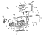
12 嵌合コネクタ
100 ネットワークコネクタ
101 サブアセンブリ
102 コア本体
104a コンタクト
104b コンタクト
106 内部プリント回路基板
108 シールド
110 磁気絶縁構成要素
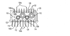
112、114 コア
116a ワイヤ
116b 電力ワイヤ
116c 接地ワイヤ
117 第1の端部
119 第2の端部
120 前端部
122 後端部
124 長手方向中間部分
125 分割パネル
126a、126b 対向側面
128 平面上部
130 平面底部
132、134 ポスト
140b コンタクト
142a、142b 貫通穴
144a、144b 空洞
146 キャッチ
148a、148b スロット
150 ハウジングシェル
151 上部
152 内部受容領域
153 後端部
154 底部
155 側面
156 底部カバー
160 嵌合インターフェース
162 嵌合コンタクト
163 インターフェース
164 係合特徴部
166 嵌合シールド
170 上部壁
172 長手方向側壁
174 前端部
176 後部壁
178 テール
179 EMIフィンガ
Claims (27)
- ネットワークコネクタであって、
幅を画定するように第1方向に沿ってそれぞれ延在する前端部及び後端部と、前記幅より大きい長さを画定するように前記前端部と前記後端部との間に延在する長手方向の中間部分とを有するコア本体であって、前記中間部分が、平面上部と、平面底部と、少なくとも1つの側面を有する平面分割パネルとを有する、コア本体と、
前記コア本体によって支持されている第1のセットのコンタクトであって、前記第1のセットのコンタクトのうちコンタクトの各々が、前記コア本体の外側に延在する露出した部分を有する、第1のセットのコンタクトと、
前記コア本体によって支持されている第2のセットのコンタクトであって、前記第2のセットのコンタクトのうちコンタクトの各々が、前記コア本体の外側に延在する露出した部分を有する、第2のセットのコンタクトと、
複数のワイヤであって、前記複数のワイヤのうちワイヤの各々が、前記第1及び第2のセットのコンタクトに結合されている、複数のワイヤと、
前記コア本体上に支持されている内部プリント回路基板であって、前記内部プリント回路基板が、前記第1のセットのコンタクトの前記露出した部分に結合されている、内部プリント回路基板と、
前記少なくとも1つの側面上に支持されており、かつ前記複数のワイヤの電気信号をフィルタリングするように構成された、磁気絶縁構成要素と、を備え、
前記第2のセットのコンタクトの前記露出した部分が、外部プリント回路基板と係合するように構成されており、
前記磁気絶縁構成要素が、少なくとも一対の磁気コアを含み、前記少なくとも一対の磁気コアは、絶縁変圧器及びコモンモードチョークを含み、前記絶縁変圧器は、前記少なくとも1つの側面に対して搭載された背面を有し、前記コモンモードチョークは、前記少なくとも1つの側面に対して搭載された背面を有するとともに、前記コア本体の前記長さに沿って前記絶縁変圧器に隣り合っており、
前記コア本体の前記前端部に結合された嵌合インターフェース部品を更に備え、前記嵌合インターフェース部品の嵌合コンタクトが、前記内部プリント回路基板に結合されている、ネットワークコネクタ。 - 前記磁気絶縁構成要素が、磁気コアを含み、各磁気コアには、前記複数のワイヤのうちの少なくとも1つが巻き付けられており、前記磁気コアが、前記コア本体の前記中間部分の前記少なくとも1つの側面に搭載されている、請求項1に記載のコネクタ。
- 前記磁気コアが、前記コア本体の前記中間部分の第2の側面に搭載されており、前記第2の側面が、前記コア本体の前記少なくとも1つの側面の反対側にある、請求項2に記載のコネクタ。
- 前記磁気絶縁構成要素が、少なくとも二対の磁気コアを含み、前記少なくとも二対の磁気コアの各々が、少なくとも1つの絶縁変圧器及び少なくとも1つのコモンモードチョークを含む、請求項1に記載のコネクタ。
- 前記少なくとも1つの側面が、実質的に平坦である、請求項2に記載のコネクタ。
- 前記中間部分の長さが、前記前端部及び前記後端部の幅の少なくとも2倍である、請求項2に記載のコネクタ。
- 前記コア本体の前記少なくとも1つの側面が、空洞を形成するように凹んでいる、請求項2に記載のコネクタ。
- 前記磁気コアが、各空洞内に収まるようにサイズ設定されている、請求項7に記載のコネクタ。
- 前記磁気コアが、第1の絶縁変圧器及び第1のコモンモードチョークを含み、かつ第2の絶縁変圧器及び第2のコモンモードチョークを含む、請求項6に記載のコネクタ。
- 前記磁気コアのうちの少なくとも1つが、4.40mm~4.80mmの範囲の外径、及び1.55mm~1.95mmの範囲の厚さを有する、請求項2に記載のコネクタ。
- 前記磁気絶縁構成要素が、樹脂又はエポキシによって前記中間部分の前記少なくとも1つの側面に固定されている、請求項1に記載のコネクタ。
- 内部受容領域及び開放された底部を有するハウジングシェルを更に備え、前記コア本体が、前記内部受容領域内に受容されており、前記第2のセットのコンタクトの前記露出した部分のうちのいくつかが、前記外部プリント回路基板に接続するために前記ハウジングシェルの前記開放された底部を通って延在する、請求項1に記載のコネクタ。
- 前記ハウジングシェルを少なくとも部分的に取り囲むシールドを更に備える、請求項12に記載のコネクタ。
- 前記シールドが、少なくとも上部壁及び対向する側壁を含み、前記上部壁が、前記ハウジングシェルの上部を覆うように構成されており、前記側壁が、前記ハウジングシェルの対向する側面を覆うように構成されている、請求項13に記載のコネクタ。
- 前記コア本体の前記前端部が、前記嵌合インターフェース部品の対応する係合特徴部と係合するための係合特徴部を含む、請求項13に記載のコネクタ。
- 前記第1のセットのコンタクト及び前記第2のセットのコンタクトが、前記コア本体の長手方向軸に概ね垂直な方向に延在する、請求項1に記載のコネクタ。
- 前記第1のセットのコンタクト及び前記第2のセットのコンタクトが、締まり嵌めによって前記コア本体に結合されている、請求項1に記載のコネクタ。
- 電力線及び接地経路をそれぞれ提供するために前記第1のセットのコンタクトと前記第2のセットのコンタクトと間に接続された、少なくとも1つの電力ワイヤと、少なくとも1つの接地ワイヤと、を更に備える、請求項1に記載のコネクタ。
- 電気コネクタであって、
内部受容領域及び開放された底部を有するハウジングシェルと、
前記ハウジングシェルの前記内部受容領域内に受容されたコア本体であって、幅を画定するように第1方向に沿ってそれぞれ延在する前端部及び後端部と、前記幅より大きい長さを画定するように前記前端部と前記後端部との間に延在する長手方向の中間部分とを有し、前記中間部分が、平面上部と、平面底部と、少なくとも1つの側面を有する平面分割パネルとを有する、コア本体と、
前記コア本体によって支持されている第1のセットのコンタクトであって、前記第1のセットのコンタクトのうちコンタクトの各々が、前記コア本体の外側に延在する露出した部分を有する、第1のセットのコンタクトと、
前記コア本体によって支持されている第2のセットのコンタクトであって、前記第2のセットのコンタクトのうちコンタクトの各々が、前記コア本体の外側に延在し、かつ前記ハウジングシェルの前記開放された底部を通って延在する、露出した部分を有する、第2のセットのコンタクトと、
前記コア本体に支持されている内部プリント回路基板であって、前記内部プリント回路基板が、前記第1のセットのコンタクトの前記露出した部分に結合されている、内部プリント回路基板と、
前記第1のセットのコンタクトと前記第2のセットのコンタクトとの間の前記少なくとも1つの側面上に搭載されたアイソレータと、
シールドと、を備え、前記シールドが、前記ハウジングシェルを少なくとも部分的に取り囲み、
前記アイソレータが、少なくとも一対の磁気コアを含み、前記少なくとも一対の磁気コアは、絶縁変圧器及びコモンモードチョークを含み、前記絶縁変圧器は、前記少なくとも1つの側面に対して搭載された背面を有し、前記コモンモードチョークは、前記少なくとも1つの側面に対して搭載された背面を有するとともに、前記コア本体の前記長さに沿って前記絶縁変圧器に隣り合っており、
前記コア本体の前記前端部に結合された嵌合インターフェース部品を更に備え、前記嵌合インターフェース部品の嵌合コンタクトが、前記内部プリント回路基板に結合されている、電気コネクタ。 - 前記中間部分の長さが、前記前端部及び前記後端部の幅の少なくとも2倍であり、少なくとも1つの側面が、実質的に平坦である、請求項19に記載のコネクタ。
- 少なくとも1つの側面が、空洞を形成するように凹んでおり、前記アイソレータが、前記空洞内に収まるように構成されている、請求項19に記載のコネクタ。
- 前記シールドが、少なくとも上部壁及び対向する側壁を含み、前記上部壁が、前記ハウジングシェルの上部を覆うように構成されており、前記側壁が、前記ハウジングシェルの対向する側面を覆うように構成されている、請求項19に記載のコネクタ。
- ネットワークコネクタを製造する方法であって、
前記ネットワークコネクタのコア本体上に複数のコンタクトを装着するステップであって、前記コア本体は、幅を画定するように第1方向に沿ってそれぞれ延在する前端部及び後端部と、前記幅より大きい長さを画定するように前記前端部と前記後端部との間に延在する長手方向の中間部分とを有し、前記中間部分が、平面上部と、平面底部と、少なくとも1つの側面を有する平面分割パネルとを有する、装着するステップと、
磁気絶縁構成要素の周りに1つ以上のワイヤを巻き付けるステップであって、前記1つ以上のワイヤが、前記複数のコンタクトに結合され、前記磁気絶縁構成要素は、少なくとも一対の磁気コアを含み、前記少なくとも一対の磁気コアは、絶縁変圧器及びコモンモードチョークを含む、巻き付けるステップと、
前記絶縁変圧器の背面が前記少なくとも1つの側面に対して搭載されるとともに、前記コモンモードチョークの背面が前記少なくとも1つの側面に対して搭載されかつ前記コア本体の前記長さに沿って前記絶縁変圧器に隣り合うように、前記磁気絶縁構成要素を前記中間部分の前記少なくとも1つの側面に対して搭載するステップと、
前記コア本体の前記複数のコンタクトに内部プリント回路基板を結合するステップと、
シールドがサブアセンブリを少なくとも部分的に取り囲むように、前記コア本体、前記複数のコンタクト、前記磁気絶縁構成要素、及び前記内部プリント回路基板のサブアセンブリの上に前記シールドを組み立てるステップと、を含み、
嵌合インターフェース部品を前記コア本体の前端部と結合し、かつ前記内部プリント回路基板を前記嵌合インターフェース部品の嵌合コンタクトに結合するステップを更に含む、方法。 - 前記コア本体、前記複数のコンタクト、前記磁気絶縁構成要素、及び前記内部プリント回路基板の前記サブアセンブリの上に前記シールドを組み立てる前記ステップの前に、前記サブアセンブリをハウジングシェルに挿入するステップを更に含む、請求項23に記載の方法。
- 前記シールドを組み立てる前記ステップが、前記シールドがハウジングシェルの上部を覆い、かつ前記ハウジングシェルの対向する側面を覆うことを含む、請求項23に記載の方法。
- 少なくとも1つの電力ワイヤを前記複数のコンタクトに結合して、少なくとも1つの電力線を提供するステップを更に含む、請求項23に記載の方法。
- 少なくとも1つの接地ワイヤを前記複数のコンタクトに結合して、少なくとも1つの接地経路を提供するステップを更に含む、請求項23に記載の方法。
Priority Applications (1)
| Application Number | Priority Date | Filing Date | Title |
|---|---|---|---|
| JP2024187591A JP2025003635A (ja) | 2021-10-29 | 2024-10-24 | 統合された磁気を備える高速ネットワークコネクタ |
Applications Claiming Priority (2)
| Application Number | Priority Date | Filing Date | Title |
|---|---|---|---|
| US17/514,175 | 2021-10-29 | ||
| US17/514,175 US12347980B2 (en) | 2021-10-29 | 2021-10-29 | High-speed network connector with integrated magnetics |
Related Child Applications (1)
| Application Number | Title | Priority Date | Filing Date |
|---|---|---|---|
| JP2024187591A Division JP2025003635A (ja) | 2021-10-29 | 2024-10-24 | 統合された磁気を備える高速ネットワークコネクタ |
Publications (2)
| Publication Number | Publication Date |
|---|---|
| JP2023067858A JP2023067858A (ja) | 2023-05-16 |
| JP7611209B2 true JP7611209B2 (ja) | 2025-01-09 |
Family
ID=84044364
Family Applications (2)
| Application Number | Title | Priority Date | Filing Date |
|---|---|---|---|
| JP2022174513A Active JP7611209B2 (ja) | 2021-10-29 | 2022-10-31 | 統合された磁気を備える高速ネットワークコネクタ |
| JP2024187591A Pending JP2025003635A (ja) | 2021-10-29 | 2024-10-24 | 統合された磁気を備える高速ネットワークコネクタ |
Family Applications After (1)
| Application Number | Title | Priority Date | Filing Date |
|---|---|---|---|
| JP2024187591A Pending JP2025003635A (ja) | 2021-10-29 | 2024-10-24 | 統合された磁気を備える高速ネットワークコネクタ |
Country Status (5)
| Country | Link |
|---|---|
| US (1) | US12347980B2 (ja) |
| EP (1) | EP4175077A1 (ja) |
| JP (2) | JP7611209B2 (ja) |
| CN (1) | CN116073161A (ja) |
| CA (1) | CA3180365A1 (ja) |
Citations (5)
| Publication number | Priority date | Publication date | Assignee | Title |
|---|---|---|---|---|
| JP2001060480A (ja) | 1998-10-29 | 2001-03-06 | Molex Inc | モジュラーコネクタ |
| JP2004186099A (ja) | 2002-12-06 | 2004-07-02 | Tdk Corp | モジュラジャック |
| US20110167869A1 (en) | 2008-08-29 | 2011-07-14 | Geers Henricus Abraham | Process and apparatus for removing gaseous contaminants from gas stream comprising gaseous contaminants |
| JP2011523541A (ja) | 2008-05-23 | 2011-08-11 | 杭州▲華▼三通信技▲術▼有限公司 | 長距離通信イーサネットシステムおよびリレー |
| JP2013510406A (ja) | 2009-11-06 | 2013-03-21 | モレックス インコーポレイテド | 強化ポートアイソレーション付きモジュラージャック |
Family Cites Families (12)
| Publication number | Priority date | Publication date | Assignee | Title |
|---|---|---|---|---|
| US5105095A (en) | 1990-08-31 | 1992-04-14 | Amp Incorporated | Data current coupler |
| US5435512A (en) | 1992-12-24 | 1995-07-25 | The Whitaker Corporation | Mounting system for current mode coupler |
| US5628653A (en) | 1996-03-12 | 1997-05-13 | Regal Electronics, Inc. | Shielded modular adapter |
| US6062908A (en) | 1997-01-27 | 2000-05-16 | Pulse Engineering, Inc. | High density connector modules having integral filtering components within repairable, replaceable submodules |
| US20020119702A1 (en) | 2000-08-22 | 2002-08-29 | John Chen | EMI suppression technique for RJ connectors with integrated magnetics |
| US7153163B2 (en) | 2002-07-16 | 2006-12-26 | Tyco Electronics Corporation | Modular jack for ethernet applications |
| US6705879B2 (en) | 2002-08-07 | 2004-03-16 | Agilent Technologies, Inc. | Pluggable electrical transceiver module with high density form factor |
| TW547854U (en) | 2002-12-25 | 2003-08-11 | Hon Hai Prec Ind Co Ltd | Electronic adapter |
| DE202004001202U1 (de) | 2004-01-28 | 2005-06-09 | Molex Incorporated, Lisle | Modulares Buchsenverbindersystem |
| WO2011056979A2 (en) | 2009-11-06 | 2011-05-12 | Molex Incorporated | Modular jack with enhanced shielding |
| US9401561B2 (en) * | 2013-07-02 | 2016-07-26 | Pulse Electronics, Inc. | Methods and apparatus for terminating wire wound electronic components to a header assembly |
| CN203481491U (zh) | 2013-08-23 | 2014-03-12 | 富士康(昆山)电脑接插件有限公司 | 电连接器 |
-
2021
- 2021-10-29 US US17/514,175 patent/US12347980B2/en active Active
-
2022
- 2022-10-28 CA CA3180365A patent/CA3180365A1/en active Pending
- 2022-10-28 EP EP22204483.6A patent/EP4175077A1/en active Pending
- 2022-10-28 CN CN202211335482.7A patent/CN116073161A/zh active Pending
- 2022-10-31 JP JP2022174513A patent/JP7611209B2/ja active Active
-
2024
- 2024-10-24 JP JP2024187591A patent/JP2025003635A/ja active Pending
Patent Citations (5)
| Publication number | Priority date | Publication date | Assignee | Title |
|---|---|---|---|---|
| JP2001060480A (ja) | 1998-10-29 | 2001-03-06 | Molex Inc | モジュラーコネクタ |
| JP2004186099A (ja) | 2002-12-06 | 2004-07-02 | Tdk Corp | モジュラジャック |
| JP2011523541A (ja) | 2008-05-23 | 2011-08-11 | 杭州▲華▼三通信技▲術▼有限公司 | 長距離通信イーサネットシステムおよびリレー |
| US20110167869A1 (en) | 2008-08-29 | 2011-07-14 | Geers Henricus Abraham | Process and apparatus for removing gaseous contaminants from gas stream comprising gaseous contaminants |
| JP2013510406A (ja) | 2009-11-06 | 2013-03-21 | モレックス インコーポレイテド | 強化ポートアイソレーション付きモジュラージャック |
Also Published As
| Publication number | Publication date |
|---|---|
| CN116073161A (zh) | 2023-05-05 |
| JP2025003635A (ja) | 2025-01-09 |
| EP4175077A1 (en) | 2023-05-03 |
| CA3180365A1 (en) | 2023-04-29 |
| JP2023067858A (ja) | 2023-05-16 |
| US20230132895A1 (en) | 2023-05-04 |
| US12347980B2 (en) | 2025-07-01 |
Similar Documents
| Publication | Publication Date | Title |
|---|---|---|
| US8992248B2 (en) | Modular jack with enhanced port isolation | |
| US9462676B2 (en) | Multi-layer circuit member with reference circuit | |
| CN102714386B (zh) | 具有增强的屏蔽的模块插座 | |
| US7959473B2 (en) | Universal connector assembly and method of manufacturing | |
| CN102124606B (zh) | 集成连接器装置和方法 | |
| KR20000035088A (ko) | 직류 감결합 및 여파 가능한 모듈형 커넥터 | |
| CN105264722B (zh) | 用于端接绕线型电子装置的方法及设备 | |
| US20110053418A1 (en) | Modular jack with two-piece housing and insert | |
| JP6663504B2 (ja) | 通信ノード | |
| TWI394319B (zh) | 電連接器 | |
| US8911257B2 (en) | Connector | |
| CN110521069B (zh) | 集成连接器模块以及用于标准化应用的印刷电路卡 | |
| US9101071B2 (en) | Magnetic element having improved transformers and common mode chokes | |
| JP7611209B2 (ja) | 統合された磁気を備える高速ネットワークコネクタ | |
| US11336065B2 (en) | Network jack with secure connector and magnetics | |
| CN113994549B (zh) | 针对ieee标准802.3bt标准的堆叠多端口10gbase-t中跨pse | |
| CN101087050B (zh) | 模组连接器 | |
| US20240072497A1 (en) | Perpendicularly mounted network jack with secure connector and magnetics |
Legal Events
| Date | Code | Title | Description |
|---|---|---|---|
| A621 | Written request for application examination |
Free format text: JAPANESE INTERMEDIATE CODE: A621 Effective date: 20221121 |
|
| A977 | Report on retrieval |
Free format text: JAPANESE INTERMEDIATE CODE: A971007 Effective date: 20231020 |
|
| A131 | Notification of reasons for refusal |
Free format text: JAPANESE INTERMEDIATE CODE: A131 Effective date: 20231113 |
|
| A601 | Written request for extension of time |
Free format text: JAPANESE INTERMEDIATE CODE: A601 Effective date: 20240213 |
|
| A521 | Request for written amendment filed |
Free format text: JAPANESE INTERMEDIATE CODE: A523 Effective date: 20240328 |
|
| A02 | Decision of refusal |
Free format text: JAPANESE INTERMEDIATE CODE: A02 Effective date: 20240624 |
|
| A521 | Request for written amendment filed |
Free format text: JAPANESE INTERMEDIATE CODE: A523 Effective date: 20241024 |
|
| A911 | Transfer to examiner for re-examination before appeal (zenchi) |
Free format text: JAPANESE INTERMEDIATE CODE: A911 Effective date: 20241031 |
|
| TRDD | Decision of grant or rejection written | ||
| A01 | Written decision to grant a patent or to grant a registration (utility model) |
Free format text: JAPANESE INTERMEDIATE CODE: A01 Effective date: 20241125 |
|
| A61 | First payment of annual fees (during grant procedure) |
Free format text: JAPANESE INTERMEDIATE CODE: A61 Effective date: 20241223 |
|
| R150 | Certificate of patent or registration of utility model |
Ref document number: 7611209 Country of ref document: JP Free format text: JAPANESE INTERMEDIATE CODE: R150 |