JP7601261B2 - Semiconductor device and its manufacturing method - Google Patents
Semiconductor device and its manufacturing method Download PDFInfo
- Publication number
- JP7601261B2 JP7601261B2 JP2023570606A JP2023570606A JP7601261B2 JP 7601261 B2 JP7601261 B2 JP 7601261B2 JP 2023570606 A JP2023570606 A JP 2023570606A JP 2023570606 A JP2023570606 A JP 2023570606A JP 7601261 B2 JP7601261 B2 JP 7601261B2
- Authority
- JP
- Japan
- Prior art keywords
- ceramic substrate
- semiconductor device
- porous sic
- metal
- holding
- Prior art date
- Legal status (The legal status is an assumption and is not a legal conclusion. Google has not performed a legal analysis and makes no representation as to the accuracy of the status listed.)
- Active
Links
Images


Classifications
-
- H10P14/2904—
-
- H10P14/6346—
-
- H10W40/10—
-
- H10W40/255—
Landscapes
- Engineering & Computer Science (AREA)
- Cooling Or The Like Of Semiconductors Or Solid State Devices (AREA)
- Microelectronics & Electronic Packaging (AREA)
- Physics & Mathematics (AREA)
- Condensed Matter Physics & Semiconductors (AREA)
- General Physics & Mathematics (AREA)
- Computer Hardware Design (AREA)
- Chemical & Material Sciences (AREA)
- Power Engineering (AREA)
- Materials Engineering (AREA)
- Manufacturing & Machinery (AREA)
- Ceramic Engineering (AREA)
- Parts Printed On Printed Circuit Boards (AREA)
- Ceramic Products (AREA)
- Die Bonding (AREA)
Description
本開示は、半導体装置及びその製造方法に関する。 The present disclosure relates to a semiconductor device and a manufacturing method thereof.
半導体チップの高温動作化により、モジュール全体の温度が上昇し、温度変化に対する寿命への影響が懸念されている。特に、はんだ接合部については、その影響を受けやすく、モジュールの寿命の大きな制約となっている。近年、はんだよりも耐ヒートサイクル性が高い、Ag系及びCu系の接合材の開発が進んでいる。しかし、チップ等の小面積接合の適用は進んでいるが、絶縁基板等の大面積接合については、接合信頼性の確保が難しい状態である。また、Ag系及びCu系接合材ははんだに比べて高価であり、大面積に使用するには適当ではない。これに対して、多孔質SiCに加圧によりAl含侵させて絶縁基板と一体成形したベース板が提案されている(例えば、特許文献1参照)が、実用化には至っていない。 As semiconductor chips operate at higher temperatures, the temperature of the entire module rises, raising concerns about the impact of temperature changes on the module's lifespan. Solder joints are particularly susceptible to this effect, which is a major constraint on the module's lifespan. In recent years, the development of Ag- and Cu-based bonding materials, which have higher heat cycle resistance than solder, has progressed. However, while the application of small-area bonding of chips and the like has progressed, it is difficult to ensure bonding reliability for large-area bonding of insulating substrates and the like. In addition, Ag- and Cu-based bonding materials are more expensive than solder and are not suitable for use over a large area. In response to this, a base plate has been proposed in which porous SiC is impregnated with Al by pressure and molded integrally with an insulating substrate (see, for example, Patent Document 1), but this has not yet been put to practical use.
特許文献1では、セラミック基板の上面と多孔質SiCの上面の高さを同じにして、両者を覆うようにアルミニウム箔を設けてセラミック基板を保持している。しかし、アルミニウム箔を設ける必要があるため、製造コストが増す。また、セラミック基板の上面と多孔質SiCの上面の高さを同じにする必要があるため、設計自由度が小さい。In Patent Document 1, the heights of the top surfaces of the ceramic substrate and the porous SiC are made the same, and aluminum foil is provided to cover both and hold the ceramic substrate. However, the need to provide the aluminum foil increases manufacturing costs. In addition, the need to make the heights of the top surfaces of the ceramic substrate and the porous SiC the same limits design freedom.
本開示は、上述のような課題を解決するためになされたもので、その目的は設計自由度が高く、製造コストを低減することができる半導体装置及びその製造方法を得るものである。 The present disclosure has been made to solve the problems described above, and its purpose is to obtain a semiconductor device and a manufacturing method thereof that have a high degree of design freedom and can reduce manufacturing costs.
本開示に係る半導体装置は、Alを主成分とする金属を含侵させた多孔質SiCと、セラミック基板と、前記セラミック基板の上に設けられた回路パターンと、前記回路パターンに接合された半導体チップとを備え、前記多孔質SiCは、前記セラミック基板を保持する保持部を有し、前記保持部は鍵状であることを特徴とする。 The semiconductor device according to the present disclosure comprises porous SiC impregnated with a metal primarily composed of Al, a ceramic substrate, a circuit pattern provided on the ceramic substrate, and a semiconductor chip bonded to the circuit pattern, wherein the porous SiC has a holding portion for holding the ceramic substrate, and the holding portion is hook-shaped .
本開示では、多孔質SiCの形状を工夫してセラミック基板を保持する保持部を設けている。従って、セラミック基板を保持するためのアルミニウム箔を設ける必要が無いため、製造コストを低減することができる。また、セラミック基板の上面と多孔質SiCの上面の高さを同じにする必要が無いため、設計自由度が大きい。In this disclosure, the shape of the porous SiC is devised to provide a holder for holding the ceramic substrate. Therefore, there is no need to provide aluminum foil to hold the ceramic substrate, which reduces manufacturing costs. In addition, there is no need to make the height of the top surface of the ceramic substrate and the top surface of the porous SiC the same, allowing for greater design freedom.
実施の形態に係る半導体装置及びその製造方法について図面を参照して説明する。同じ又は対応する構成要素には同じ符号を付し、説明の繰り返しを省略する場合がある。The semiconductor device and the manufacturing method thereof according to the embodiment will be described with reference to the drawings. The same or corresponding components will be given the same reference numerals, and repeated explanations may be omitted.
実施の形態1.
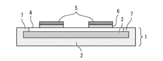
図1は、実施の形態1に係る半導体装置を示す断面図である。図2は、実施の形態1に係る半導体装置を示す上面図である。この半導体装置はパワーモジュールである。一体型ベース板1は、Alを主成分とする金属を含侵させた多孔質SiC2と、セラミック基板3と、セラミック基板3の上に設けられた回路パターン4とを有する。多孔質SiC2は、セラミック基板3を保持する保持部7を有する。保持部7は、セラミック基板3の外周全体を囲んでセラミック基板3を保持する。
Embodiment 1.
Fig. 1 is a cross-sectional view showing a semiconductor device according to a first embodiment. Fig. 2 is a top view showing the semiconductor device according to the first embodiment. This semiconductor device is a power module. The integrated base plate 1 has
一体型ベース板1の厚みは例えば3mm以上8mm以下である。一体型ベース板1は高い放熱性を有しているが、その放熱性は主にセラミック基板3に因る。セラミック基板3は、例えば、アルミナ(Al2O3)、窒化アルミニウム(AlN)、窒化ケイ素(SiN)などからなる。
The thickness of the integrated base plate 1 is, for example, 3 mm to 8 mm. The integrated base plate 1 has high heat dissipation properties, which are mainly due to the
半導体チップ5が回路パターン4にはんだ材、Ag焼結材又はCu焼結材などの接合材6により接合されている。半導体チップ5は例えばSiのIGBT及びダイオード、SiCのMOSFET及びSBDなどである。半導体チップ5の上面電極はワイヤ(不図示)により端子(不図示)に電気的に接続されている。なお、一体型ベース板1に外装ケースを取り付けてもよい。さらに、その外装ケース内を封止樹脂で封止してもよい。The
続いて、本実施の形態の半導体装置の製造方法について説明する。図3は、実施の形態1に係る半導体装置の製造方法を説明するための図である。まず、SiC(スラリ)を鋳造し、焼結して形成した多孔質SiC2を切削加工して保持部7を形成する。または、3Dプリンターを用いて、保持部7を有する多孔質SiC2を形成してもよい。次に、成形された多孔質SiC2の保持部7にセラミック基板3を保持させる。Next, a method for manufacturing a semiconductor device according to the present embodiment will be described. FIG. 3 is a diagram for explaining a method for manufacturing a semiconductor device according to the first embodiment. First, SiC (slurry) is cast and sintered to form porous SiC2, which is then machined to form the
次に、セラミック基板3を装着した多孔質SiC2を、一体型ベース板1の形状をなす金型8の中に配置する。例えば無加圧含侵、加圧含侵、又はダイカストなどによりAlを主成分とする金属9を多孔質SiC2に含侵させる。次に、セラミック基板3の上面に残った金属9をエッチングして回路パターン4を形成する。その後、半導体チップ5を回路パターン4に接合材6により接合し、ワイヤボンディング等を行う。Next, the
従来は、セラミック基板の上面と多孔質SiCの上面の高さを同じにして、両者を覆うようにアルミニウム箔を設けてセラミック基板を保持していた。これに対して、本実施の形態では、多孔質SiC2の形状を工夫してセラミック基板3を保持する保持部7を設けている。従って、セラミック基板3を保持するためのアルミニウム箔を設ける必要が無いため、製造コストを低減することができる。また、セラミック基板3の上面と多孔質SiC2の上面の高さを同じにする必要が無いため、設計自由度が大きい。Conventionally, the upper surface of the ceramic substrate and the upper surface of the porous SiC were made to be at the same height, and aluminum foil was provided to cover both to hold the ceramic substrate. In contrast, in this embodiment, the shape of the
また、はんだ接合なしにセラミック基板3とベース板の一体化を実現している。一体型ベース板1は高い放熱性を有しているため、耐ヒートサイクル性と高放熱化を実現することができる。
In addition, the
また、多孔質SiC2に金属を含侵させる際に無加圧含侵を用いることが好ましい。無加圧含侵であれば加圧による含侵に比べてプロセスを簡略化できる。また、多孔質SiC2に金属9を含侵させた後にセラミック基板3の上の金属9をエッチングして回路パターン4を形成する。これによりプロセスが簡略化されて製造コストを低減できる。
It is also preferable to use pressureless impregnation when impregnating the porous SiC2 with metal. Pressureless impregnation can simplify the process compared to impregnation using pressure. After impregnating the porous SiC2 with the
実施の形態2.
図4は、実施の形態2に係る半導体装置を示す上面図である。セラミック基板3は平面視で四角形である。多孔質SiC2は、3箇所以上でセラミック基板3の側面に接してセラミック基板3を保持する保持部7を有する。保持部7は、四角形のセラミック基板3の異なる3辺をそれぞれ保持する。保持部7が設けられていない部分からセラミック基板3を保持部7の内側に挿入する。
4 is a top view showing a semiconductor device according to
3箇所以上の保持部7によりセラミック基板3の位置が決定される。また、セラミック基板3に対する応力を緩和することができる。また、多孔質SiC2がセラミック基板の側面全面に接する実施の形態1に比べ原材料の削減が可能となり、特に3Dプロリンターで多孔質SiC2を形成する場合に特に製造コストを低減できる。その他の構成及び効果は実施の形態1と同様である。
The position of the
実施の形態3.
図5は、実施の形態3に係る半導体装置を示す断面図である。多孔質SiC2はセラミック基板3を保持する鍵状の保持部7を有する。鍵状の保持部7はセラミック基板3の側面と上面を抱き込むように設けられている。これにより、セラミック基板3が含侵時にずれるのを防ぐことができる。従って、含侵時のプロセスマージンを確保し、生産性を向上させることができる。その他の構成及び効果は実施の形態2と同様である。
5 is a cross-sectional view showing a semiconductor device according to the third embodiment. The
実施の形態4.
図6は、実施の形態4に係る半導体装置を示す断面図である。保持部7はセラミック基板3の異なる3辺をそれぞれ保持するように設けられている。保持部7が設けられていないセラミック基板3の1辺側を、含侵時に金属9を供給する湯口側とする。これにより、湯口側からの金属9の流動性を確保しつつ、セラミック基板3の位置決めと保持を実現することができる。その他の構成及び効果は実施の形態3と同様である。
6 is a cross-sectional view showing a semiconductor device according to a fourth embodiment. The holding
実施の形態5.
図7は、実施の形態5に係る半導体装置を示す上面図である。実施の形態1では大判のセラミック基板3を1枚だけ用いていたが、本実施の形態ではセラミック基板3は2枚以上に分割されている。多孔質SiC2は、分割された2枚以上のセラミック基板3を保持する。大判のセラミック基板よりも安価な個片のセラミック基板を使用することで、製造コストを低減することができる。また、セラミック基板3に対する応力を緩和することができる。その他の構成及び効果は実施の形態1と同様である。
7 is a top view showing a semiconductor device according to a fifth embodiment. In the first embodiment, only one large
なお、半導体チップ5は、珪素によって形成されたものに限らず、珪素に比べてバンドギャップが大きいワイドバンドギャップ半導体によって形成されたものでもよい。ワイドバンドギャップ半導体は、例えば、炭化珪素、窒化ガリウム系材料、又はダイヤモンドである。このようなワイドバンドギャップ半導体によって形成された半導体チップは、耐電圧性及び許容電流密度が高いため、小型化できる。この小型化された半導体チップを用いることで、この半導体チップを組み込んだ半導体装置も小型化・高集積化できる。また、半導体チップの耐熱性が高いため、ヒートシンクの放熱フィンを小型化でき、水冷部を空冷化できるので、半導体装置を更に小型化できる。また、半導体チップの電力損失が低く高効率であるため、半導体装置を高効率化できる。
The
2 多孔質SiC、3 セラミック基板、4 回路パターン、5 半導体チップ、7 保持部、9 金属 2 Porous SiC, 3 Ceramic substrate, 4 Circuit pattern, 5 Semiconductor chip, 7 Holding portion, 9 Metal
Claims (10)
セラミック基板と、
前記セラミック基板の上に設けられた回路パターンと、
前記回路パターンに接合された半導体チップとを備え、
前記多孔質SiCは、前記セラミック基板を保持する保持部を有し、
前記保持部は鍵状であることを特徴とする半導体装置。 Porous SiC impregnated with a metal mainly composed of Al;
A ceramic substrate;
a circuit pattern provided on the ceramic substrate;
a semiconductor chip bonded to the circuit pattern,
the porous SiC has a holding portion for holding the ceramic substrate,
The semiconductor device, wherein the holding portion is hook-shaped .
前記保持部は前記セラミック基板の異なる3辺をそれぞれ保持することを特徴とする請求項3に記載の半導体装置。 The ceramic substrate is rectangular in plan view,
4. The semiconductor device according to claim 3, wherein the holding portions respectively hold three different sides of the ceramic substrate.
セラミック基板を前記保持部に保持させる工程と、
Alを主成分とする金属を前記多孔質SiCに含侵させる工程と、
前記多孔質SiCに前記金属を含侵させた後に、前記セラミック基板の上面の残った前記金属をエッチングして回路パターンを形成する工程と、
前記回路パターンに半導体チップを接合する工程とを備え、
前記多孔質SiCに前記金属を含侵させる際に無加圧含侵を用いることを特徴とする半導体装置の製造方法。 forming a porous SiC having a retaining portion;
a step of holding the ceramic substrate on the holding part;
impregnating the porous SiC with a metal mainly composed of Al;
after impregnating the porous SiC with the metal, etching the remaining metal on the top surface of the ceramic substrate to form a circuit pattern;
and bonding a semiconductor chip to the circuit pattern .
A method for manufacturing a semiconductor device, comprising the steps of: impregnating the porous SiC with the metal without applying pressure ;
セラミック基板を前記保持部に保持させる工程と、
Alを主成分とする金属を前記多孔質SiCに含侵させる工程と、
前記多孔質SiCに前記金属を含侵させた後に、前記セラミック基板の上面の残った前記金属をエッチングして回路パターンを形成する工程と、
前記回路パターンに半導体チップを接合する工程とを備え、
前記保持部が設けられていない前記セラミック基板の1辺側を、含侵時に前記金属を供給する湯口側とすることを特徴とする半導体装置の製造方法。 forming a porous SiC having a retaining portion;
a step of holding the ceramic substrate on the holding part;
impregnating the porous SiC with a metal mainly composed of Al;
after impregnating the porous SiC with the metal, etching the remaining metal on the top surface of the ceramic substrate to form a circuit pattern;
and bonding a semiconductor chip to the circuit pattern.
A method for manufacturing a semiconductor device, comprising : forming a sprue side of the ceramic substrate on which the holding portion is not provided, the sprue side through which the metal is supplied during impregnation.
Applications Claiming Priority (1)
| Application Number | Priority Date | Filing Date | Title |
|---|---|---|---|
| PCT/JP2021/048880 WO2023127130A1 (en) | 2021-12-28 | 2021-12-28 | Semiconductor device and method for producing same |
Publications (2)
| Publication Number | Publication Date |
|---|---|
| JPWO2023127130A1 JPWO2023127130A1 (en) | 2023-07-06 |
| JP7601261B2 true JP7601261B2 (en) | 2024-12-17 |
Family
ID=86998432
Family Applications (1)
| Application Number | Title | Priority Date | Filing Date |
|---|---|---|---|
| JP2023570606A Active JP7601261B2 (en) | 2021-12-28 | 2021-12-28 | Semiconductor device and its manufacturing method |
Country Status (5)
| Country | Link |
|---|---|
| US (1) | US20240274500A1 (en) |
| JP (1) | JP7601261B2 (en) |
| CN (1) | CN118414700A (en) |
| DE (1) | DE112021008560T5 (en) |
| WO (1) | WO2023127130A1 (en) |
Citations (3)
| Publication number | Priority date | Publication date | Assignee | Title |
|---|---|---|---|---|
| JP2003297988A (en) | 2002-04-05 | 2003-10-17 | Denki Kagaku Kogyo Kk | Structure |
| WO2016017689A1 (en) | 2014-07-31 | 2016-02-04 | 電気化学工業株式会社 | Aluminum-silicon carbide composite and production method therefor |
| JP2021004668A (en) | 2019-06-27 | 2021-01-14 | 京セラ株式会社 | Passage member |
Family Cites Families (1)
| Publication number | Priority date | Publication date | Assignee | Title |
|---|---|---|---|---|
| JPH08191120A (en) * | 1995-01-10 | 1996-07-23 | Hitachi Ltd | Substrate for power semiconductor device and manufacturing method thereof |
-
2021
- 2021-12-28 JP JP2023570606A patent/JP7601261B2/en active Active
- 2021-12-28 WO PCT/JP2021/048880 patent/WO2023127130A1/en not_active Ceased
- 2021-12-28 US US18/690,472 patent/US20240274500A1/en active Pending
- 2021-12-28 CN CN202180105114.0A patent/CN118414700A/en active Pending
- 2021-12-28 DE DE112021008560.3T patent/DE112021008560T5/en active Pending
Patent Citations (3)
| Publication number | Priority date | Publication date | Assignee | Title |
|---|---|---|---|---|
| JP2003297988A (en) | 2002-04-05 | 2003-10-17 | Denki Kagaku Kogyo Kk | Structure |
| WO2016017689A1 (en) | 2014-07-31 | 2016-02-04 | 電気化学工業株式会社 | Aluminum-silicon carbide composite and production method therefor |
| JP2021004668A (en) | 2019-06-27 | 2021-01-14 | 京セラ株式会社 | Passage member |
Also Published As
| Publication number | Publication date |
|---|---|
| WO2023127130A1 (en) | 2023-07-06 |
| JPWO2023127130A1 (en) | 2023-07-06 |
| CN118414700A (en) | 2024-07-30 |
| US20240274500A1 (en) | 2024-08-15 |
| DE112021008560T5 (en) | 2024-10-31 |
Similar Documents
| Publication | Publication Date | Title |
|---|---|---|
| US8569890B2 (en) | Power semiconductor device module | |
| KR100957078B1 (en) | Electrically Isolated Power Device Package | |
| KR102418458B1 (en) | Power semiconductor module | |
| JP6699742B2 (en) | Semiconductor device | |
| US20150221525A1 (en) | Semiconductor device and method of manufacture thereof | |
| CN101335263A (en) | Semiconductor module and method for manufacturing semiconductor module | |
| JP6907670B2 (en) | Semiconductor devices and methods for manufacturing semiconductor devices | |
| JP3972821B2 (en) | Power semiconductor device | |
| CN110021565B (en) | Encapsulated leadless package with at least partially exposed inner sidewalls of chip carrier | |
| JP2012209470A (en) | Semiconductor device, semiconductor device module, and manufacturing method of the semiconductor device | |
| CN111433910B (en) | Semiconductor device and method of manufacturing semiconductor device | |
| JP7601261B2 (en) | Semiconductor device and its manufacturing method | |
| EP3739624A1 (en) | Semiconductor arrangement with a compressible contact element encapsulated between two carriers and corresponding manufacturing method | |
| KR102714726B1 (en) | Ceramic substrate for power module, manufacturing method thereof and power module with the same | |
| JPH11214612A (en) | Power semiconductor module | |
| KR20230034618A (en) | Ceramic substrate for power module, manufacturing method thereof and power module with the same | |
| JP7480715B2 (en) | Semiconductor Device | |
| KR102603439B1 (en) | Semiconductor package having negative patterned substrate and method of fabricating the same | |
| CN118398561A (en) | Stress relief structure as lateral edge portion of semiconductor body | |
| CN119234310A (en) | Semiconductor device and method for manufacturing the same | |
| JP2022044158A (en) | Method for manufacturing semiconductor module | |
| JP2007027261A (en) | Power module | |
| KR102588851B1 (en) | Power module and manufacturing method thereof | |
| KR102882682B1 (en) | Manufacturing method of pin-fin base plate integrated ceramic heat dissipation substrate and manufacturing method of power module package including the substrate | |
| JP7484766B2 (en) | Semiconductor Module |
Legal Events
| Date | Code | Title | Description |
|---|---|---|---|
| A621 | Written request for application examination |
Free format text: JAPANESE INTERMEDIATE CODE: A621 Effective date: 20231211 |
|
| A131 | Notification of reasons for refusal |
Free format text: JAPANESE INTERMEDIATE CODE: A131 Effective date: 20240903 |
|
| A521 | Request for written amendment filed |
Free format text: JAPANESE INTERMEDIATE CODE: A523 Effective date: 20240918 |
|
| TRDD | Decision of grant or rejection written | ||
| A01 | Written decision to grant a patent or to grant a registration (utility model) |
Free format text: JAPANESE INTERMEDIATE CODE: A01 Effective date: 20241105 |
|
| A61 | First payment of annual fees (during grant procedure) |
Free format text: JAPANESE INTERMEDIATE CODE: A61 Effective date: 20241118 |
|
| R150 | Certificate of patent or registration of utility model |
Ref document number: 7601261 Country of ref document: JP Free format text: JAPANESE INTERMEDIATE CODE: R150 |