JP7588937B2 - Power Amplifiers - Google Patents
Power Amplifiers Download PDFInfo
- Publication number
- JP7588937B2 JP7588937B2 JP2020209599A JP2020209599A JP7588937B2 JP 7588937 B2 JP7588937 B2 JP 7588937B2 JP 2020209599 A JP2020209599 A JP 2020209599A JP 2020209599 A JP2020209599 A JP 2020209599A JP 7588937 B2 JP7588937 B2 JP 7588937B2
- Authority
- JP
- Japan
- Prior art keywords
- phase
- positive
- negative
- signal
- overcurrent detection
- Prior art date
- Legal status (The legal status is an assumption and is not a legal conclusion. Google has not performed a legal analysis and makes no representation as to the accuracy of the status listed.)
- Active
Links
- 238000001514 detection method Methods 0.000 claims description 199
- 230000005236 sound signal Effects 0.000 claims description 4
- 238000010586 diagram Methods 0.000 description 18
- 101100433746 Arabidopsis thaliana ABCG29 gene Proteins 0.000 description 4
- 101100433754 Arabidopsis thaliana ABCG30 gene Proteins 0.000 description 4
- 102000012677 DET1 Human genes 0.000 description 4
- 101150113651 DET1 gene Proteins 0.000 description 4
- 101100054289 Oryza sativa subsp. japonica ABCG34 gene Proteins 0.000 description 4
- 101100054291 Oryza sativa subsp. japonica ABCG35 gene Proteins 0.000 description 4
- 101100107595 Oryza sativa subsp. japonica ABCG41 gene Proteins 0.000 description 4
- 101100107601 Oryza sativa subsp. japonica ABCG45 gene Proteins 0.000 description 4
- 101150088582 PDR1 gene Proteins 0.000 description 4
- 101150024488 PDR2 gene Proteins 0.000 description 4
- 101100321174 Saccharomyces cerevisiae (strain ATCC 204508 / S288c) YRR1 gene Proteins 0.000 description 4
- 101100400877 Trichophyton rubrum (strain ATCC MYA-4607 / CBS 118892) MDR1 gene Proteins 0.000 description 4
- 238000002844 melting Methods 0.000 description 4
- 230000008018 melting Effects 0.000 description 4
- 239000004065 semiconductor Substances 0.000 description 4
- 239000003990 capacitor Substances 0.000 description 2
- 230000000630 rising effect Effects 0.000 description 2
- 230000001360 synchronised effect Effects 0.000 description 2
- 101100484492 Arabidopsis thaliana VHA-C gene Proteins 0.000 description 1
- 101150066284 DET2 gene Proteins 0.000 description 1
- 101000746134 Homo sapiens DNA endonuclease RBBP8 Proteins 0.000 description 1
- 101000969031 Homo sapiens Nuclear protein 1 Proteins 0.000 description 1
- 102100021133 Nuclear protein 1 Human genes 0.000 description 1
- 101100206695 Rattus norvegicus Thoc6 gene Proteins 0.000 description 1
- 102100029469 WD repeat and HMG-box DNA-binding protein 1 Human genes 0.000 description 1
- 101710097421 WD repeat and HMG-box DNA-binding protein 1 Proteins 0.000 description 1
- 238000007796 conventional method Methods 0.000 description 1
- 230000000694 effects Effects 0.000 description 1
- 230000005669 field effect Effects 0.000 description 1
- 229910044991 metal oxide Inorganic materials 0.000 description 1
- 150000004706 metal oxides Chemical class 0.000 description 1
- 238000000034 method Methods 0.000 description 1
- 238000012986 modification Methods 0.000 description 1
- 230000004048 modification Effects 0.000 description 1
- 238000012544 monitoring process Methods 0.000 description 1
- 230000010355 oscillation Effects 0.000 description 1
- 230000005855 radiation Effects 0.000 description 1
- 230000001629 suppression Effects 0.000 description 1
Images


Landscapes
- Amplifiers (AREA)
Description
本発明は、電力増幅器に係り、特に、半導体上に出力段がBTL(Bridged Trans Less)接続を用いて構成されてなる電力増幅器における出力同時天絡、同時地絡時の過電流に対する安全対策費用削減、回路の安全性、信頼性の向上等を図ったものに関する。 The present invention relates to a power amplifier, and in particular to a power amplifier in which the output stage is configured on a semiconductor using a BTL (Bridged Transformer Less) connection, which aims to reduce the cost of safety measures against overcurrents caused by simultaneous output shorts to the power supply and simultaneous output shorts to the ground, and to improve the safety and reliability of the circuit.
オーディオパワーアンプは、8Ω、4Ωなどの重負荷のスピーカを駆動するため、サイズの大きいパワートランジスタを用いて入力信号を電力増幅するのが一般的である。そのようなパワートランジスタを用いた電力増幅器の出力端子が、天絡、又は、地絡した場合、大電流による焼損の危険性が高いため過電流検出回路を内蔵するのが一般的である。
係る過電流検出回路は、例えば、特許文献1に開示されたようにパワートランジスタの電流をモニターする方法等が知られており、さらに、過電流検出回路の検出精度向上や電力損失の低減を図った構成が特許文献2等において開示されている。
Audio power amplifiers generally use large-sized power transistors to amplify the power of the input signal in order to drive speakers with heavy loads such as 8Ω, 4Ω, etc. If the output terminal of a power amplifier using such power transistors is shorted to the power supply or ground, there is a high risk of burning due to the large current, so an overcurrent detection circuit is generally built in.
As such an overcurrent detection circuit, for example, a method of monitoring the current of a power transistor as disclosed in Patent Document 1 is known, and furthermore, a configuration for improving the detection accuracy of the overcurrent detection circuit and reducing power loss is disclosed in
図6には、このような従来の電力増幅器の一回路構成例が示されており、以下、同図を参照しつつ、この従来回路について説明する。
この電力増幅器は、正相入力信号INPと逆相入力信号INNとが、それぞれ基本的に同一構成の増幅回路により増幅されて、BTL接続された負荷RLを駆動可能に構成されてなるものである。
すなわち、正相入力信号INPは、第1のドライブ回路PDR1を介してプッシュプル接続された2つのパワートランジスタQ1,Q2により増幅され、その正相増幅出力OUTPは負荷RLの一端に印加される構成となっている。
また、逆相入力信号INNは、第2のドライブ回路PDR2を介してプッシュプル接続された2つのパワートランジスタQ3,Q4により増幅され、その逆相増幅出力OUTNは負荷RLの他端に印加される構成となっている。
FIG. 6 shows an example of a circuit configuration of such a conventional power amplifier, and this conventional circuit will be described below with reference to the same figure.
This power amplifier is configured so that a positive-phase input signal INP and a negative-phase input signal INN are amplified by amplifier circuits each having a basically identical configuration, and are capable of driving a BTL-connected load RL.
That is, the positive phase input signal INP is amplified by two power transistors Q1 and Q2 connected in a push-pull manner via a first drive circuit PDR1, and the positive phase amplified output OUTP is applied to one end of a load RL.
The negative-phase input signal INN is amplified by two power transistors Q3 and Q4 connected in a push-pull manner via a second drive circuit PDR2, and the negative-phase amplified output OUTN is applied to the other end of the load RL.
また、パワートランジスタQ1,Q2に流れる電流は、検出用トランジスタQd1,Qd2によりモニターされ、所定の第1の電流値を超えた場合に第1及び第2の検出回路DET1,DET2から過電流検出信号が出力されるようになっている。
同様に、パワートランジスタQ3,Q4に流れる電流は、検出用トランジスタQd3,Qd4によりモニターされ、所定の第1の電流値を超えた場合に第3及び第4の検出回路DET3,DET4から過電流の検出信号が出力されるようになっている。
In addition, the current flowing through the power transistors Q1, Q2 is monitored by detection transistors Qd1, Qd2, and when the current exceeds a predetermined first current value, an overcurrent detection signal is output from the first and second detection circuits DET1, DET2.
Similarly, the current flowing through the power transistors Q3, Q4 is monitored by detection transistors Qd3, Qd4, and when the current exceeds a predetermined first current value, an overcurrent detection signal is output from the third and fourth detection circuits DET3, DET4.
第1乃至第4の検出回路DET1~DET4からの検出信号は、論理和回路ORを介して過電流検出信号OCDETとして、第1及び第2のドライブ回路PDR1,PDR2へ入力され、動作停止信号として機能するようになっている。すなわち、第1乃至第4の検出回路DET1~DET4のいずれからの検出信号に対応して論理和回路ORを介して過電流検出信号OCDETが出力され、第1及び第2のドライブ回路PDR1,PDR2に入力されると、第1及び第2のドライブ回路PDR1,PDR2は動作停止し、パワートランジスタQ1~Q4が駆動停止されるようになっている。 The detection signals from the first to fourth detection circuits DET1 to DET4 are input to the first and second drive circuits PDR1, PDR2 as an overcurrent detection signal OCDET via the logical OR circuit OR, and function as an operation stop signal. That is, when the overcurrent detection signal OCDET is output via the logical OR circuit OR in response to a detection signal from any of the first to fourth detection circuits DET1 to DET4 and input to the first and second drive circuits PDR1, PDR2, the first and second drive circuits PDR1, PDR2 stop operating, and the power transistors Q1 to Q4 are stopped from being driven.
ここで、第1乃至第4の検出回路DET1~DET4が検出信号OCDETを出力する基準となる第1の電流値は、アプリケーションの最大電流よりも大きな値に設定され、アプリケーションの最大電流Ioutmaxは、下記する式1により算出される。 Here, the first current value, which is the reference for the first to fourth detection circuits DET1 to DET4 to output the detection signal OCDET, is set to a value greater than the maximum current of the application, and the maximum current Ioutmax of the application is calculated by the following formula 1.
Ioutmax=(Poutmax/RL)1/2×21/2・・・式1 Ioutmax=(Poutmax/RL) 1/2 ×2 1/2 ...Formula 1
なお、ここで、Poutmaxは電力増幅器の最大出力電力、RLは負荷抵抗値とする。
例えば、負荷抵抗値RL=4Ω、最大出力電力Poutmax=8Wの電力増幅器の場合、アプリケーションの最大電流は2Aと算出される。したがって、この場合、第1の電流値は2Aを超える適宜な値、例えば、2.5Aなどに設定される。
上述のようにして第1の電流値が決定された後、この電流値においてボンディングワイヤの溶断が生じないようにボンディングワイヤの本数が決定されることとなる。
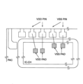
例えば、図7に模式的に示されたように、上述のような過電流に対処するために、半導体ICパッケージPACに搭載されたICチップIC-CHにおいては、電源電圧用ボンディングパッドVDD PADやグランド用ボンディングパッドVSS PADを増設して、半導体ICパッケージPACの外周近傍に設けられた電源電圧用接続ピンVDD PINやグランド用接続ピンVSS PINと、対応するボンディングパッドとを接続するボンディングワイヤを増設することで、ボンディングワイヤ一本あたりに流れる電流を減らす対策が採られる。
Here, Poutmax is the maximum output power of the power amplifier, and RL is the load resistance value.
For example, in the case of a power amplifier having a load resistance value RL=4Ω and a maximum output power Poutmax=8 W, the maximum current of the application is calculated to be 2 A. Therefore, in this case, the first current value is set to an appropriate value exceeding 2 A, for example, 2.5 A.
After the first current value is determined as described above, the number of bonding wires is determined so that the bonding wires will not melt at this current value.
For example, as shown in FIG. 7, in order to deal with the above-mentioned overcurrent, in the IC chip IC-CH mounted on the semiconductor IC package PAC, a power supply voltage bonding pad VDD PAD and a ground bonding pad VSS PAD are added, and bonding wires are added to connect the power supply voltage connection pin VDD PIN and the ground connection pin VSS PIN provided near the outer periphery of the semiconductor IC package PAC to the corresponding bonding pads, thereby reducing the current flowing through each bonding wire.
ここで、正相増幅出力OUTP、逆相増幅出力OUTNが同時天絡、同時地絡する場合について考える。同時天絡、同時地絡が発生した場合、先の第1の電流値の2倍が電源端子VDD、又は、グランド端子VSSに流れる虞がある。そのため、このような場合にも、ボンディングワイヤが溶断しないようにするためには、電源端子VDD、及び、グランド端子VSSには、ボンディングワイヤのさらなる増設、強化が必要となる。
そのため、ボンディングワイヤの本数増加とボンディングパッド数の増加による製品原価の高騰を招くという問題がある。
Here, consider the case where the positive-phase amplified output OUTP and the negative-phase amplified output OUTN are simultaneously shorted to power or ground. If a simultaneous short to power or ground occurs, there is a risk that twice the first current value will flow to the power supply terminal VDD or the ground terminal VSS. Therefore, in order to prevent the bonding wires from melting even in such a case, it is necessary to further increase and strengthen the bonding wires at the power supply terminal VDD and the ground terminal VSS.
This leads to a problem of a rise in product costs due to an increase in the number of bonding wires and bonding pads.
本発明は、上記実状に鑑みてなされたもので、ボンディングワイヤの本数増加やボンディングパッド数の増加を招くことなく、同時天絡、同時短絡時の過電流に対する回路の安全確保、信頼性の向上可能な電力増幅器を提供するものである。 The present invention has been made in consideration of the above-mentioned circumstances, and provides a power amplifier that can ensure the safety of the circuit against overcurrents caused by simultaneous short circuits to the power supply or simultaneous short circuits, and can improve reliability, without increasing the number of bonding wires or bonding pads.
上記本発明の目的を達成するため、本発明に係る電力増幅器は、
正相入力信号を増幅する正相信号増幅部と、逆相入力信号を増幅する逆相信号増幅部とを有し、前記正相信号増幅部の出力と前記逆相信号増幅部の出力がBTL接続で負荷に供給可能に構成されると共に、前記正相信号増幅部における第1の電流値を超える過電流の発生と、前記逆相信号増幅部における第1の電流値を超える過電流の発生とを、それぞれ検出可能に構成された過電流検出部とを有してなる電力増幅器であって、
前記過電流検出部は、前記正相信号増幅部と前記逆相信号増幅部における同時天絡の発生、又は、前記正相信号増幅部と前記逆相信号増幅部における同時地絡の発生により、前記正相信号増幅部と前記逆相信号増幅部のそれぞれにおける第2の電流値を超える過電流の発生を検出可能に構成されると共に、前記第1の電流値を超える過電流、又は、前記第2の電流値を超える過電流のいずれかが検出された場合に、前記正相信号増幅部及び前記逆相信号増幅部に対して統合過電流検出信号を出力し、
前記正相信号増幅部及び前記逆相信号増幅部は、前記統合過電流検出信号が出力された際に、それぞれ動作停止可能に構成されてなり、
前記正相信号増幅部は、正相パワートランジスタドライブ回路と、正相第1及び第2のパワートランジスタと、正相第1及び第2のモニタトランジスタとを有し、PチャンネルMOSFETの前記正相第1のパワートランジスタと、NチャンネルMOSFETの前記正相第2のパワートランジスタは、ドレインが相互に接続され、前記正相第1のパワートランジスタのソースには電源電圧が印可可能とされ、前記正相第2のパワートランジスタのソースはグランドに接続され、
前記正相第1及び第2のパワートランジスタは、外部から正相入力信号が入力される前記正相パワートランジスタドライブ回路のドライブ信号が、前記正相第1及び第2のパワートランジスタの各々のゲートに入力されることで駆動可能とされ、
PチャンネルMOSFETの前記正相第1のモニタトランジスタとNチャンネルMOSFETの前記正相第2のモニタトランジスタは、ドレインが相互に接続されると共に、前記正相第1及び第2のパワートランジスタのドレイン相互の接続点及び前記負荷の一端が接続される正相出力端子に接続され、
前記正相第1のモニタトランジスタのソースは、正相第1の検出抵抗器を介して前記電源電圧が印加可能とされ、
前記正相第2のモニタトランジスタのソースは、正相第2の検出抵抗器を介してグランドに接続され、
前記逆相信号増幅部は、逆相パワートランジスタドライブ回路と、逆相第1及び第2のパワートランジスタと、逆相第1及び第2のモニタトランジスタとを有し、PチャンネルMOSFETの前記逆相第1のパワートランジスタと、NチャンネルMOSFETの前記逆相第2のパワートランジスタは、ドレインが相互に接続され、前記逆相第1のパワートランジスタのソースには前記電源電圧が印可可能とされ、前記逆相第2のパワートランジスタのソースはグランドに接続され、
前記逆相第1及び第2のパワートランジスタは、外部から逆相入力信号が入力される前記逆相パワートランジスタドライブ回路のドライブ信号が、前記逆相第1及び第2のパワートランジスタの各々のゲートに入力されることで駆動可能とされ、
PチャンネルMOSFETの前記逆相第1のモニタトランジスタとNチャンネルMOSFETの前記逆相第2のモニタトランジスタは、ドレインが相互に接続されると共に、前記逆相第1及び第2のパワートランジスタのドレイン相互の接続点及び前記負荷の他端が接続される逆相出力端子に接続され、
前記正相出力端子と前記逆相出力端子の間には、前記負荷が接続され、
前記逆相第1のモニタトランジスタのソースは、逆相第1の検出抵抗器を介して前記電源電圧が印加可能とされ、
前記逆相第2のモニタトランジスタのソースは、逆相第2の検出抵抗器を介してグランドに接続され、
前記過電流検出部は、正相第1基準第1及び第2の過電流検出回路と、逆相第1基準第1及び第2の過電流検出回路と、正相第2基準第1及び第2の過電流検出回路と、逆相第2基準第1及び第2の過電流検出回路とを有し、
前記正相第1のモニタトランジスタのソースと前記正相第1の検出抵抗器との接続点は、前記正相第1基準第1の過電流検出回路及び前記正相第2基準第1の過電流検出回路の入力段に接続され、
前記正相第2のモニタトランジスタのソースと前記正相第2の検出抵抗器との接続点は、前記正相第1基準第2の過電流検出回路及び前記正相第2基準第2の過電流検出回路の入力段に接続され、
前記逆相第1のモニタトランジスタのソースと前記逆相第1の検出抵抗器との接続点は、前記逆相第1基準第1の過電流検出回路及び前記逆相第2基準第1の過電流検出回路の入力段に接続され、
前記逆相第2のモニタトランジスタのソースと前記逆相第2の検出抵抗器との接続点は、前記逆相第1基準第2の過電流検出回路及び前記逆相第2基準第2の過電流検出回路の入力段に接続され、
前記正相出力端子と逆相出力端子における同時地絡の発生により、前記正相第1のモニタトランジスタにより検出された前記正相第1のパワートランジスタの電流が、前記正相第2基準第1の過電流検出回路によって前記第2の電流値を超える過電流と判定され、前記逆相第1のモニタトランジスタにより検出された前記逆相第1のパワートランジスタの電流が、前記逆相第2基準第1の過電流検出回路によって前記第2の電流値を超える過電流と判定された場合に、前記過電流検出部による前記正相信号増幅部及び前記逆相信号増幅部に対する前記統合過電流検出信号が出力され、
前記正相出力端子と逆相出力端子における同時天絡の発生により、前記正相第2のモニタトランジスタにより検出された前記正相第2のパワートランジスタの電流が、前記正相第2基準第2の過電流検出回路によって前記第2の電流値を超える過電流と判定され、前記逆相第2のモニタトランジスタにより検出された前記逆相第2のパワートランジスタの電流が、前記逆相第2基準第2の過電流検出回路によって前記第2の電流値を超える過電流と判定された場合に、前記過電流検出部による前記正相信号増幅部及び前記逆相信号増幅部に対する前記統合過電流検出信号が出力されるよう構成されてなるものである。
In order to achieve the above object of the present invention, a power amplifier according to the present invention comprises:
A power amplifier comprising: a positive-phase signal amplifier section for amplifying a positive-phase input signal; and a negative-phase signal amplifier section for amplifying a negative-phase input signal, wherein an output of the positive-phase signal amplifier section and an output of the negative-phase signal amplifier section can be supplied to a load via a BTL connection; and an overcurrent detection section configured to detect an occurrence of an overcurrent exceeding a first current value in the positive-phase signal amplifier section and an occurrence of an overcurrent exceeding the first current value in the negative-phase signal amplifier section,
the overcurrent detection unit is configured to be able to detect an occurrence of an overcurrent exceeding a second current value in each of the positive-phase signal amplifier unit and the negative-phase signal amplifier unit due to a simultaneous power short in the positive-phase signal amplifier unit and the negative-phase signal amplifier unit, or a simultaneous ground short in the positive-phase signal amplifier unit and the negative-phase signal amplifier unit, and outputs an integrated overcurrent detection signal to the positive-phase signal amplifier unit and the negative-phase signal amplifier unit when either an overcurrent exceeding the first current value or an overcurrent exceeding the second current value is detected;
the positive-phase signal amplifier and the negative-phase signal amplifier are each configured to be stopped when the integrated overcurrent detection signal is output,
the positive phase signal amplifier section has a positive phase power transistor drive circuit, positive phase first and second power transistors, and positive phase first and second monitor transistors, the positive phase first power transistor being a P-channel MOSFET and the positive phase second power transistor being an N-channel MOSFET, the drains of which are connected to each other, a power supply voltage can be applied to the source of the positive phase first power transistor, and the source of the positive phase second power transistor is connected to ground,
the first and second positive phase power transistors can be driven by a drive signal of the positive phase power transistor drive circuit to which a positive phase input signal is input from an external source, being input to the gates of the first and second positive phase power transistors,
the positive phase first monitor transistor which is a P-channel MOSFET and the positive phase second monitor transistor which is an N-channel MOSFET have drains which are connected to each other and are also connected to a positive phase output terminal to which a connection point between the drains of the positive phase first and second power transistors and one end of the load are connected;
the power supply voltage can be applied to a source of the first positive phase monitor transistor via a first positive phase detection resistor;
a source of the second positive phase monitor transistor is connected to ground via a second positive phase detection resistor;
the negative-phase signal amplifier section has a negative-phase power transistor drive circuit, negative-phase first and second power transistors, and negative-phase first and second monitor transistors, the drains of the negative-phase first power transistor which is a P-channel MOSFET and the negative-phase second power transistor which is an N-channel MOSFET are connected to each other, the power supply voltage can be applied to the source of the negative-phase first power transistor, and the source of the negative-phase second power transistor is connected to ground,
the first and second negative-phase power transistors can be driven by a drive signal of the negative-phase power transistor drive circuit to which an external negative-phase input signal is input, being input to each gate of the first and second negative-phase power transistors;
the drains of the negative-phase first monitor transistor which is a P-channel MOSFET and the drains of the negative-phase second monitor transistor which is an N-channel MOSFET are connected to each other and to a negative-phase output terminal to which a connection point between the drains of the negative-phase first and second power transistors and the other end of the load are connected;
the load is connected between the positive phase output terminal and the negative phase output terminal;
the power supply voltage can be applied to a source of the negative-phase first monitor transistor via a negative-phase first detection resistor;
a source of the inverted second monitor transistor is connected to ground via an inverted second sense resistor;
the overcurrent detection unit includes positive-phase first-reference first and second overcurrent detection circuits, negative-phase first-reference first and second overcurrent detection circuits, positive-phase second-reference first and second overcurrent detection circuits, and negative-phase second-reference first and second overcurrent detection circuits;
a connection point between a source of the positive-phase first monitor transistor and the positive-phase first detection resistor is connected to an input stage of the positive-phase first reference first overcurrent detection circuit and the positive-phase second reference first overcurrent detection circuit;
a connection point between a source of the positive-phase second monitor transistor and the positive-phase second detection resistor is connected to an input stage of the positive-phase first reference second overcurrent detection circuit and the positive-phase second reference second overcurrent detection circuit;
a connection point between a source of the negative-phase first monitor transistor and the negative-phase first detection resistor is connected to an input stage of the negative-phase first reference first overcurrent detection circuit and the negative-phase second reference first overcurrent detection circuit;
a connection point between a source of the negative-phase second monitor transistor and the negative-phase second detection resistor is connected to an input stage of the negative-phase first reference second overcurrent detection circuit and the negative-phase second reference second overcurrent detection circuit;
when a simultaneous ground fault occurs at the positive-phase output terminal and the negative-phase output terminal, the current of the positive-phase first power transistor detected by the positive-phase first monitor transistor is determined to be an overcurrent exceeding the second current value by the positive-phase second reference first overcurrent detection circuit, and the current of the negative-phase first power transistor detected by the negative-phase first monitor transistor is determined to be an overcurrent exceeding the second current value by the negative-phase second reference first overcurrent detection circuit, the overcurrent detection unit outputs the integrated overcurrent detection signal to the positive-phase signal amplifier unit and the negative-phase signal amplifier unit,
When a simultaneous short circuit to power occurs at the positive-phase output terminal and the negative-phase output terminal, the current of the positive-phase second power transistor detected by the positive-phase second monitor transistor is determined to be an overcurrent exceeding the second current value by the positive-phase second reference second overcurrent detection circuit, and the current of the negative-phase second power transistor detected by the negative-phase second monitor transistor is determined to be an overcurrent exceeding the second current value by the negative-phase second reference second overcurrent detection circuit, the overcurrent detection unit outputs the integrated overcurrent detection signal to the positive-phase signal amplifier unit and the negative-phase signal amplifier unit .
本発明によれば、出力端の同時天絡や同時地絡が生じた際に、出力端の一方に天絡、又は、地絡が生じた場合の過電流検出の基準である従来の第1の電流値とは別個の第2の電流値によって過電流の発生が検出されるように構成したので、従来と異なり、同時天絡、同時地絡発生時におけるボンディングワイヤ溶断回避のためのボンディングの本数増加やボンディングパッドの増加を伴うことなく、回路の安全性確実、信頼性の向上を図ることができるという効果を奏するものである。 According to the present invention, when simultaneous power shorts or ground shorts occur at the output terminals, the occurrence of an overcurrent is detected by a second current value that is different from the conventional first current value that is the standard for overcurrent detection when a power short or ground short occurs at one of the output terminals. Therefore, unlike the conventional method, it is possible to improve the safety and reliability of the circuit without increasing the number of bonds or bonding pads to avoid bonding wire meltdown when simultaneous power shorts or ground shorts occur.
以下、本発明の実施の形態について、図1乃至図5を参照しつつ説明する。
なお、以下に説明する部材、配置等は本発明を限定するものではなく、本発明の趣旨の範囲内で種々改変することができるものである。
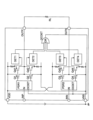
最初に、本発明の実施の形態における電力増幅器の第1の回路構成例について、図1を参照しつつ説明する。
この電力増幅器は、正相信号増幅部101と、逆相信号増幅部102と、過電流検出部103とに大別されて構成されたものとなっている。
正相信号増幅部101と逆相信号増幅部102の各々の増幅出力信号は、BTL接続により負荷(図1においては「RL」と表記)37に供給される構成となっている。
DETAILED DESCRIPTION OF THE PREFERRED EMBODIMENTS Hereinafter, an embodiment of the present invention will be described with reference to FIGS.
It should be noted that the components, arrangements, etc. described below do not limit the present invention, and various modifications can be made within the scope of the present invention.
First, a first example of a circuit configuration of a power amplifier according to an embodiment of the present invention will be described with reference to FIG.
This power amplifier is roughly divided into a positive-
The amplified output signals of the positive-
過電流検出部103は、従来同様、正相出力端子93における天絡、又は、地絡、若しくは、逆相出力端子94における天絡、又は、地絡による過電流の発生を、正相第1基準第1及び第2の過電流検出回路61,62、逆相第1基準第1及び第2の過電流検出回路71,72により行い、過電流が検出された際に正相信号増幅部101及び逆相信号増幅部102の動作が遮断されるようになっている(詳細は後述)。
As in the past, the
さらに、本発明の実施の形態における過電流検出部103は、従来と異なり、正相信号増幅部101と逆相信号増幅部102における同時天絡、同時地絡による出力電流の過電流検出が過電流検出部103によって行われ、過電流が検出された際に正相信号増幅部101及び逆相信号増幅部102の動作が遮断されるようになっている(詳細は後述)。
Furthermore, unlike conventional devices, the
正相信号増幅部101は、正相パワートランジスタドライブ回路(図1においては「PDRP」と表記)51と、正相第1及び第2のパワートランジスタ(図1においては、それぞれ「M1HP」、「M2LP」と表記)1,2と、正相第1及び第2のモニタトランジスタ(図1においては、それぞれ「Mm1HP」、「Mm2LP」と表記)5,6とを主たる構成要素として構成されてなるものである。
また、逆相信号増幅部102は、被増幅信号が逆相入力信号という点では、正相信号増幅部と異なるが、基本的な構成は正相信号増幅部101と同様である。
The positive
The negative-
すなわち、逆相信号増幅部102は、逆相パワートランジスタドライブ回路(図1においては「PDRN」と表記)52と、逆相第1及び第2のパワートランジスタ(図1においては、それぞれ「M1HN」、「M2LN」と表記)3,4と、逆相第1及び第2のモニタトランジスタ(図1においては、それぞれ「Mm1HN」、「Mm2LN」と表記)7,8とを主たる構成要素として構成されてなるものである。
That is, the negative-
過電流検出部103は、正相第1基準第1及び第2の過電流検出回路(図1においては、それぞれ「L1DTHP」、「L1DTLP」と表記)61,62と、逆相第1基準第1及び第2の過電流検出回路(図1においては、それぞれ「L1DTHN」、「L1DTLN」と表記)71,72と、正相第2基準第1及び第2の過電流検出回路(図1においては、それぞれ「L2DTHP」、「L2DTLP」と表記)63,64と、逆相第2基準第1及び第2の過電流検出回路(図1においては、それぞれ「L2DTHN」、「L2DTLN」と表記)73,74と、第1及び第2のAND回路(図1においては、それぞれ「AND1」、「AND2」と表記)11,12と、6入力論理和回路(図1においては「OR」と表記)13とを主たる構成要素として構成されたものとなっている。
The
本発明の実施の形態において、正相信号増幅部101における正相第1のパワートランジスタ1には、PチャンネルMOSFET(Metal Oxide Semiconductor Field-Effect Transistor)が、正相第2のパワートランジスタ2には、NチャンネルMOSFETが、それぞれ用いられている。
この正相第1及び第2のパワートランジスタ1,2は、電源端子95とグランド端子96との間にプッシュプル接続されて設けられている。
すなわち、正相第1及び第2のパワートランジスタ1,2は、ドレインが相互に接続されて、正相第1のパワートランジスタ1のソースは電源端子95に、正相第2のパワートランジスタ2のソースは、グランド端子96に、それぞれ接続されている。
なお、電源端子95とグランド端子96の間には、直流電源40が接続されている。
In the embodiment of the present invention, a P-channel Metal Oxide Semiconductor Field-Effect Transistor (MOSFET) is used for the positive phase first power transistor 1 in the positive
The first and second positive-
That is, the drains of the first and second positive-
A
正相パワートランジスタドライブ回路51は、正相入力端子91を介して正相入力信号が入力され、そのドライブ信号を正相第1及び第2のパワートランジスタ1,2のゲートへ出力することで正相第1及び第2のパワートランジスタ1,2が駆動されるようになっている。
また、正相パワートランジスタドライブ回路51は、後述するように、過電流検出部103の統合過電流検出信号OCDETが論理値Highに相当するレベルとなると動作停止し、正相第1及び第2のパワートランジスタ1,2の動作を遮断できるようになっている。
The positive phase power
As will be described later, the positive-phase power
さらに、本発明の実施の形態において、正相第1のモニタトランジスタ5には、PチャンネルMOSFETが、正相第2のモニタトランジスタ6には、NチャンネルMOSFETが、それぞれ用いられている。
正相第1及び第2のモニタトランジスタ5,6は、ドレインが相互に接続されると共に、正相第1及び第2のパワートランジスタ1,2のドレイン相互の接続点と正相出力端子93に接続されている。
Furthermore, in the embodiment of the present invention, a P-channel MOSFET is used for the positive-phase
The drains of the first and second positive-
また、正相第1のモニタトランジスタ5のソースは、正相第1の検出抵抗器(図1においては「R1HP」と表記)21を介して電源端子95に印加される電源電圧VDDが印加されるようになっている。また、正相第1のモニタトランジスタ5のソースと正相第1の検出抵抗器21との接続点は、正相第1基準第1の過電流検出回路61及び正相第2基準第1の過電流検出回路63の入力段に接続されている。
The source of the first positive-
一方、正相第2のモニタトランジスタ6のソースは、正相第2の検出抵抗器(図1においては「R2LP」と表記)22及びグランド端子96を介してグランド電位に維持されるようになっている。また、正相第2のモニタトランジスタ6のソースと正相第2の検出抵抗器22との接続点は、正相第1基準第2の過電流検出回路62及び正相第2基準第2の過電流検出回路64の入力段に接続されている。
On the other hand, the source of the positive-phase
次に、逆相信号増幅部102における逆相第1のパワートランジスタ3には、PチャンネルMOSFETが、逆相第2のパワートランジスタ4には、NチャンネルMOSFETが、それぞれ用いられている。
この逆相第1及び第2のパワートランジスタ3,4は、電源端子95とグランド端子96との間にプッシュプル接続されて設けられている。
Next, a P-channel MOSFET is used for the negative-phase
The first and second reverse-
すなわち、逆相第1及び第2のパワートランジスタ3,4は、ドレインが相互に接続されて、逆相第1のパワートランジスタ3のソースは電源端子95に、逆相第2のパワートランジスタ4のソースは、グランド端子96に、それぞれ接続されている。
逆相パワートランジスタドライブ回路52は、逆相入力端子92を介して逆相入力信号が入力され、そのドライブ信号を逆相第1及び第2のパワートランジスタ3,4のゲートへ出力することで逆相第1及び第2のパワートランジスタ3,4を駆動されるようになっている。
That is, the drains of the negative-phase first and
The negative-phase power
また、逆相パワートランジスタドライブ回路52は、後述するように、過電流検出部103の統合過電流検出信号OCDETが論理値Highに相当するレベルとなると動作停止し、逆相第1及び第2のパワートランジスタ3,4の動作を遮断できるようになっている。
本発明の実施の形態において、逆相第1のモニタトランジスタ7には、PチャンネルMOSFETが、逆相第2のモニタトランジスタ8には、NチャンネルMOSFETが、それぞれ用いられている。
As will be described later, the negative-phase power
In the embodiment of the present invention, a P-channel MOSFET is used for the negative phase
逆相第1及び第2のモニタトランジスタ7,8は、ドレインが相互に接続されると共に、逆相第1及び第2のパワートランジスタ3,4のドレイン相互の接続点と逆相出力端子94に接続されている。
また、逆相第1のモニタトランジスタ7のソースは、逆相第1の検出抵抗器(図1においては「R1HN」と表記)23を介して電源端子95に印加される電源電圧VDDが印加されるようになっている。また、逆相第1のモニタトランジスタ7のソースと逆相第1の検出抵抗器23との接続点は、逆相第1基準第1の過電流検出回路71及び逆相第2基準第1の過電流検出回路73の入力段に接続されている。
The drains of the negative-phase first and
The source of the negative-phase
一方、逆相第2のモニタトランジスタ8のソースは、逆相第2の検出抵抗器(図1においては「R2LN」と表記)24及びグランド端子96を介してグランド電位に維持されるようになっている。また、逆相第2のモニタトランジスタ8のソースと逆相第2の検出抵抗器24との接続点は、逆相第1基準第2の過電流検出回路72及び逆相第2基準第2の過電流検出回路74の入力段に接続されている。
On the other hand, the source of the negative-phase
正相第1基準第1及び第2の過電流検出回路61,62と、逆相第1基準第1及び第2の過電流検出回路71,72の各々の出力は、6入力論理和回路13に入力されている。
また、正相第2基準第1の過電流検出回路63の出力と、逆相第2基準第1の過電流検出回路73の出力は、第1のAND回路11に入力されて、その論理積出力が6入力論理和回路13に入力されるようになっている。
The outputs of the positive-phase first-reference first and second
In addition, the output of the positive phase second reference first
さらに、正相第2基準第2の過電流検出回路64の出力と、逆相第2基準第2の過電流検出回路74の出力は、第2のAND回路12に入力されて、その論理積出力が6入力論理和回路13に入力されるようになっている。
6入力論理和回路13は、6つの入力のいずれかが論理値Highとなった場合に、それを統合過電流検出信号OCDETとして出力する。
6入力論理和回路13の出力端子は、正相パワートランジスタドライブ回路51と逆相パワートランジスタドライブ回路52のそれぞれの統合過電流検出信号入力端子OCDETに接続されている。
Furthermore, the output of the positive phase second reference second
When any one of the six inputs of the six-input OR
The output terminal of the six-input OR
次に、上記構成における回路動作について説明する。
まず、正相入力端子91に外部から入力された正相信号INPは、正相パワートランジスタドライブ回路51、正相第1及び第2のパワートランジスタ1,2により電力増幅され、正相出力端子93から正相出力信号OUTPとして出力される。
また、逆相入力端子92に外部から入力された逆相信号INNは、逆相パワートランジスタドライブ回路52、逆相第1及び第2のパワートランジスタ3,4により電力増幅され、逆相出力端子94から逆相出力信号OUTNとして出力され、正相出力端子93と逆相出力端子94の間に接続された負荷37はBTL駆動されることとなる。
Next, the circuit operation in the above configuration will be described.
First, a positive phase signal INP input from outside to a positive
In addition, the negative phase signal INN input from outside to the negative
一方、過電流検出部103においては、正相第1のモニタトランジスタ5により正相第1のパワートランジスタ1の電流が、正相第2のモニタトランジスタ6により正相第2のパワートランジスタ2の電流が、それぞれ検出され、その検出電流が、正相第1基準第1及び第2の過電流検出回路61,62、及び、正相第2基準第1及び第2の過電流検出回路63,64において、それぞれの基準を超えているか否かが判定される。
On the other hand, in the
すなわち、正相第1のパワートランジスタ1の電流が第1の基準電流値を超えた場合、正相第1基準第1の過電流検出回路61から論理値Highに相当するレベルの検出信号(以下説明の便宜上、「正相第1基準第1トランジスタ過電流検出信号」と称する)が、正相第2のパワートランジスタ2の電流が第1の基準電流値を超えた場合、正相第1基準第2の過電流検出回路62から論理値Highに相当するレベルの検出信号(以下説明の便宜上、「正相第1基準第2トランジスタ過電流検出信号」と称する)が、それぞれ出力される。
That is, when the current of the positive-phase first power transistor 1 exceeds the first reference current value, the positive-phase first reference first
また、逆相第1のパワートランジスタ3の電流が第1の基準電流値を超えた場合、逆相第1基準第1の過電流検出回路71から論理値Highに相当するレベルの検出信号(以下説明の便宜上、「逆相第1基準第1トランジスタ過電流検出信号」と称する)が、逆相第2のパワートランジスタ4の電流が第1の基準電流値を超えた場合、逆相第1基準第2の過電流検出回路72から論理値Highに相当するレベルの検出信号(以下説明の便宜上、「逆相第1基準第2トランジスタ過電流検出信号」と称する)が、それぞれ出力される。
When the current of the negative-phase
さらに、正相第1のパワートランジスタ1の電流が第2の基準電流値を超えた場合、正相第2基準第1の過電流検出回路63から論理値Highに相当するレベルの検出信号(以下説明の便宜上、「正相第2基準第1トランジスタ過電流検出信号」と称する)が、正相第2のパワートランジスタ2の電流が第2の基準電流値を超えた場合、正相第2基準第2の過電流検出回路64から論理値Highに相当するレベルの検出信号(以下説明の便宜上、「正相第2基準第2トランジスタ過電流検出信号」と称する)が、それぞれ出力される。
Furthermore, when the current of the positive-phase first power transistor 1 exceeds the second reference current value, the positive-phase second reference first
またさらに、逆相第1のパワートランジスタ3の電流が第2の基準電流値を超えた場合、逆相第2基準第1の過電流検出回路73から論理値Highに相当するレベルの検出信号(以下説明の便宜上、「逆相第2基準第1トランジスタ過電流検出信号」と称する)が、逆相第2のパワートランジスタ4の電流が第2の基準電流値を超えた場合、逆相第2基準第2の過電流検出回路74から論理値Highに相当するレベルの検出信号(以下説明の便宜上、「逆相第2基準第2トランジスタ過電流検出信号」と称する)が、それぞれ出力される。
Furthermore, when the current of the negative-phase
そして、正相1基準第1の過電流検出回路61、正相1基準第2の過電流検出回路62、逆相1基準第1の過電流検出回路71、及び、逆相1基準第2の過電流検出回路72のいずれかから論理値Highに相当するレベルの検出信号が出力された場合に、6入力論理和回路13から同じく論理値Highに相当するレベルの統合過電流検出信号OCDETが出力され、正相パワートランジスタドライブ回路51及び逆相パワートランジスタドライブ回路52にそれぞれ入力される。
When a detection signal having a level equivalent to a logical high is output from any of the positive phase 1 reference first
その結果、正相パワートランジスタドライブ回路51、逆相パワートランジスタドライブ回路52による正相第1及び第2のパワートランジスタ1,2、逆相第1及び第2のパワートランジスタ3,4の駆動が停止され、正相第1及び第2のパワートランジスタ1,2、逆相第1及び第2のパワートランジスタ3,4は、遮断状態となる。
As a result, the positive-phase power
また、第1のAND回路11、又は、第2のAND回路12のいずれかの出力が論理値Highに相当するレベルとなった場合にも、上述と同様に、6入力論理和回路13から同じく論理値Highに相当するレベルの統合過電流検出信号OCDETが出力され、正相第1及び第2のパワートランジスタ1,2、逆相第1及び第2のパワートランジスタ3,4が遮断状態とされる。
Also, when the output of either the first AND
すなわち、正相第2基準第1の過電流検出回路63と逆相第2基準第1の過電流検出回路73の双方において第2の電流値を超える過電流が検出された場合、第1のAND回路11から論理値Highに相当するレベルの検出信号(以下説明の便宜上、「同時地絡過電流検出信号」と称する)が出力される。
また、正相第2基準第2の過電流検出回路64と逆相第2基準第2の過電流検出回路74の双方において第2の電流値を超える過電流が検出された場合、第2のAND回路12から論理値Highに相当するレベルの検出信号(以下説明の便宜上、「同時天絡過電流検出信号」と称する)が出力される。
In other words, when an overcurrent exceeding the second current value is detected in both the positive phase second reference first
In addition, when an overcurrent exceeding the second current value is detected in both the positive phase second reference second
正相第1基準第1及び第2の過電流検出回路61,62、逆相第1基準第1及び第2の過電流検出回路71,72は、基本的に従来と同様に、正相出力端子93又は逆相出力端子94における天絡、又は、地絡の発生によって正相第1、第2のパワートランジスタ1、2、逆相第1、第2のパワートランジスタ3、4のいずれかに過電流が生ずることを検出するために設けられている。そして、過電流検出の基準となる第1の電流値は、従来同様、先の式1により求められるアプリケーション(電力増幅器の具体的な使用形態)の最大電流Ioutmaxを超える適宜な値に選定されるものとなっている。
The positive-phase first reference first and second
一方、正相出力端子93と逆相出力端子94における同時天絡、又は、同時地絡の発生により、正相第1のパワートランジスタ1に第2の電流値を超える過電流が生じたことを検出する正相第2基準第1の過電流検出回路63、正相第2のパワートランジスタ2に第2の電流値を超える過電流が生じたことを検出する正相第2基準第2の過電流検出回路64、逆相第1のパワートランジスタ3に第2の電流値を超える過電流が生じたことを検出する逆相第2基準第1の過電流検出回路73、及び、逆相第2のパワートランジスタ4に第2の電流値を超える過電流が生じたことを検出する逆相第2基準第2の過電流検出回路74における過電流検出の基準である第2の電流値は、次述するような観点から定められる。
On the other hand, the second current value, which is the reference for overcurrent detection in the positive-phase second reference first
まず、負荷に対する電力供給が本発明の実施の形態の電力増幅器のようにBTL接続で行われる回路の場合、一方の出力が電流をソースするときに、もう一方は電流をシンクするため、通常動作において、ハイサイドトランジスタである正相第1のパワートランジスタ1と逆相第1のパワートランジスタ3が同時に大電流をソースすることはなく、また、ローサイドパワートランジスタである正相第2のパワートランジスタ2と逆相第2のパワートランジスタ4が同時に大電流をシンクすることはない。
First, in the case of a circuit in which power is supplied to a load by a BTL connection, such as the power amplifier of the embodiment of the present invention, when one output sources a current, the other sinks a current, so in normal operation, the high-side transistors, the positive-phase first power transistor 1 and the negative-phase
そのため、第2の電流値は、先の第1の電流値と異なり、式1により求められるアプリケーションの最大電流を考慮することなく第1の電流値よりも十分小さな値に設定することができる。すなわち、パワートランジスタに対する過電流によるダメージをより早期に解消し、回路保護を図ることが可能となる。
なお、第2の電流値の具体的な値は、電力増幅器の具体的な仕様や、使用形態等を考慮して、個々に適切な値を選定することとなる。
Therefore, unlike the above-described first current value, the second current value can be set to a value sufficiently smaller than the first current value without considering the maximum current of the application calculated by Equation 1. In other words, damage to the power transistor caused by an overcurrent can be eliminated more quickly, and the circuit can be protected.
The specific value of the second current value is selected as an appropriate value for each power amplifier, taking into consideration the specific specifications of the power amplifier, the manner in which it is used, and the like.
上述の構成例において、正相入力信号と逆相入力信号は、交互に正負にレベル変化する信号を想定しているが、このような信号に限定される必要はなく、第1の回路構成例は、3値パルス幅変調信号を用いる場合も有効である。
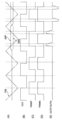
図3には、3値パルス幅変調信号の生成に適する3値パルス幅変調回路の回路構成例が、図4には、3値パルス幅変調回路の動作を説明する波形図が、それぞれ示されており、以下、これらの図を参照しつつ3値パルス幅変調信号について説明する。
In the above-described configuration example, the positive phase input signal and the negative phase input signal are assumed to be signals whose levels alternate between positive and negative, but there is no need to be limited to such signals, and the first circuit configuration example is also effective in the case where a ternary pulse width modulated signal is used.
FIG. 3 shows an example of a circuit configuration of a ternary pulse width modulation circuit suitable for generating a ternary pulse width modulation signal, and FIG. 4 shows a waveform diagram explaining the operation of the ternary pulse width modulation circuit. Below, the ternary pulse width modulation signal will be explained with reference to these figures.
最初に、図3に示された3値パルス幅変調回路について説明する。
この3値パルス幅変調回路は、第1及び第2のコンパレータ(図3においては、それぞれ「COM1」、「COM2」と表記)41,42と、三角波発振器(図3においては「OSC」と表記)43を有して構成されている。
第1及び第2のコンパレータ41,42の各々の反転入力端子は、相互に接続されて三角波発振器43の出力段に接続されている。
First, the ternary pulse width modulation circuit shown in FIG. 3 will be described.
This three-value pulse width modulation circuit is configured with first and second comparators (denoted as “COM1” and “COM2” in FIG. 3, respectively) 41, 42, and a triangular wave oscillator (denoted as “OSC” in FIG. 3) 43.
The inverting input terminals of the first and
また、第1のコンパレータ41には、第1の回路構成例と同様な正相入力信号INPが、第2のコンパレータ42には、同じく逆相入力信号INNが、それぞれ入力されるようになっている。
三角波発振器43には、後述するようなクロック信号CLKが入力され、このクロック信号CLKに同期した三角波信号TWが生成、出力され、第1及び第2のコンパレータ41,42へ入力されるようになっている。
The
A clock signal CLK, as described below, is input to the
次に、図4を参照しつつ、図3に示された3値パルス幅変調回路と電力増幅器の動作について説明する。
三角波発振器43から出力される三角波信号TW(図4(A)二点鎖線参照)は、アナログオーディオ信号である正相入力信号、逆相入力信号に比して繰り返し周波数が十分高く設定されたものとなっている(図4(B)参照)。すなわち、三角波発振器43に入力されるクロック信号CLK(図4(B)参照)の繰り返し周波数は、アナログオーディオ信号に対して高い周波数に設定されている。
Next, the operation of the ternary pulse width modulation circuit and the power amplifier shown in FIG. 3 will be described with reference to FIG.
The triangular wave signal TW (see the two-dot chain line in FIG. 4A) output from the
第1のコンパレータ41において、正相アナログ入力信号INPが無入力時には、第1のコンパレータ41からはデューティ50%の繰り返しパルス信号が出力されるが、無入力時以外においては、三角波信号が正相アナログ入力信号INPを下回ったところでハイレベルとなり、三角波信号が正相アナログ入力信号INPを上回ったところでローレベルとなる第1のパルス幅変調信号PWMPが出力される(図4(A)及び図4(C)参照)。
When there is no positive-phase analog input signal INP input to the
また、第2のコンパレータ42においても、逆相アナログ入力信号INNが無入力時には、第2のコンパレータ41からはデューティ50%の繰り返しパルス信号が出力されるが、無入力時以外においては、三角波信号が逆相アナログ入力信号INNを下回ったところでハイレベルとなり、三角波信号が逆相アナログ入力信号INNを上回ったところでローレベルとなる第2のパルス幅変調信号PWMNが出力される(図4(A)及び図4(D)参照)。
In the
上述の第1のパルス幅変調信号PWMPは正相入力端子91へ入力され、正相信号増幅部101により増幅されて正相出力信号OUTPとして正相出力端子93へ出力される一方、第2のパルス幅変調信号PWMNは逆相入力端子92へ入力され、逆相信号増幅部102により増幅されて逆相出力信号OUTNとして逆相出力端子94へ出力される。
正相アナログ入力信号INPと逆相アナログ入力信号INNが無信号時には、第1のパルス幅変調信号PWMPと第2のパルス幅変調信号PWMNの差分はゼロとなる。その結果、負荷37には、図4(E)に示されたようにハイレベル、ゼロ、マイナスハイレベルの3値パルス幅変調信号が与えられることとなる。
The above-mentioned first pulse width modulation signal PWMP is input to a positive
When the positive-phase analog input signal INP and the negative-phase analog input signal INN are not present, the difference between the first pulse-width modulated signal PWMP and the second pulse-width modulated signal PWMN is 0. As a result, a ternary pulse-width modulated signal of high level, zero, and minus high level is applied to the
このような3値パルス幅変調信号を用いた場合、入力信号が無信号の場合、先に説明したように正相出力信号OUTPと逆相出力信号OUTNの差分がゼロとなるため、出力LCフィルタを介して負荷をBTLで駆動する必要がなく、出力LCフィルタの省略によるコストダウンが可能となる。
その一方で、3値パルス幅変調信号は、同時にハイレベル、同時にローレベルとなる場合があるため、同時天絡、同時地絡の発生を考慮する必要があるが、本発明の実施の形態における電力増幅器は、係る同時天絡、同時地絡による過電流に起因する回路素子の焼損等を確実に抑圧、防止可能であり、3値パルス幅変調信号を用いる場合に好適である。
When such a three-value pulse width modulated signal is used, if there is no input signal, the difference between the positive phase output signal OUTP and the negative phase output signal OUTN becomes zero as explained above, so there is no need to drive the load with a BTL via an output LC filter, making it possible to reduce costs by omitting the output LC filter.
On the other hand, since a ternary pulse width modulated signal may be at a high level and a low level simultaneously, it is necessary to take into consideration the occurrence of simultaneous shorts to power and shorts to ground. However, the power amplifier in the embodiment of the present invention can reliably suppress and prevent the burning of circuit elements caused by overcurrent due to such simultaneous shorts to power and shorts to ground, and is suitable for use with a ternary pulse width modulated signal.
しかし、高出力化に伴う高電源電圧化による輻射ノイズの影響を考慮する必要がある場合には、3値パルス幅変調信号を用いても出力LCフィルタを介して負荷をBTL接続で駆動する構成を採ることとなる。
無入力時における第1のパルス幅変調信号PWMP及び第2のパルス幅変調信号PWMNは、先に説明したようにデューティ50%であるため、電源電圧VDDの半分の電圧値をバイアスポイントとして動作することとなる。したがって、動作開始時に、出力LCフィルタにVDD/2のインパルスが入力し、LC共振による電流の減衰振動が発生する。
However, when it is necessary to take into consideration the effects of radiation noise due to the higher power supply voltage accompanying higher output, a configuration will be adopted in which the load is driven by a BTL connection via an output LC filter even if a three-value pulse width modulation signal is used.
As described above, the first pulse width modulation signal PWMP and the second pulse width modulation signal PWMN have a duty of 50% when no input is applied, and therefore operate with a voltage value that is half the power supply voltage VDD as a bias point. Therefore, at the start of operation, an impulse of VDD/2 is input to the output LC filter, and a damped oscillation of the current occurs due to LC resonance.
通常、LCフィルタで用いるインダクタの直列抵抗値Rは小さく、LCR回路にインパルス入力がなされたときの電流IFILTERは、下記する式2で表される。
Normally, the series resistance R of the inductor used in an LC filter is small, and the current I FILTER when an impulse is input to an LCR circuit is expressed by the
IFILTER=(VDD/2)/{L/C-(R/2)2}1/2×e-(R/2L)t×sin[t{1/LC-(R/2L)2}1/2]・・・式2
IFILTER=(VDD/2)/{L/C-(R/2) 2 } 1/2 ×e -(R/2L)t ×sin[t{1/LC-(R/2L) 2 } 1/ 2 ]...
したがって、式2で表されるインパルス信号起因の電流が、正相第2基準第1及び第2の過電流検出回路63,64、及び、逆相第2基準第1及び第2の過電流検出回路73,74における第2の電流値を超え、本来不要な過電流検出が行われてしまうという問題が生ずる可能性がある。
Therefore, the current caused by the impulse signal expressed by
このような問題を回避する方策としては、第2の電流値を大きくすることが必要とされるが、それは、ボンディングパッド増加やボンディングワイヤ増加を招いてしまう。
図2には、出力LCフィルタを設けることにより生ずる上述のような問題の解決に適する第2の回路構成例が示されており、以下、同図を参照しつつ、第2の回路構成例について説明する。
なお、図1に示された構成要素と同一の構成要素については、同一の符号を付して、その詳細な説明を省略し、以下、異なる点を中心に説明する。
この第2の回路構成例は、図1に示された第1の回路構成例に、インパルス信号起因の電流が第2の電流値を超えた場合に過電流検出信号の出力を回避するための論理回路(詳細は後述)を付加した構成を有するものである。
To avoid such a problem, it is necessary to increase the second current value, but this leads to an increase in the number of bonding pads and bonding wires.
FIG. 2 shows a second circuit configuration example suitable for solving the above-mentioned problems caused by the provision of an output LC filter. Hereinafter, the second circuit configuration example will be described with reference to the same figure.
The same components as those shown in FIG. 1 are denoted by the same reference numerals, and detailed description thereof will be omitted. The following description will focus on the differences.
This second circuit configuration example has a configuration in which a logic circuit (described in detail later) for avoiding output of an overcurrent detection signal when a current caused by an impulse signal exceeds a second current value is added to the first circuit configuration example shown in FIG. 1 .
すなわち、この電力増幅器は、過電流検出部103において、第1及び第2のAND回路11,12の後段に、NOT回路14、第1及び第2のDフリップフロップ15,16、2入力論理和回路17、及び、カウンタ回路18、並びに、6入力論理和回路13に代えて5入力論理和回路(図2においては「OR2」と表記)19による論理回路が増設された構成を有してなるものである。さらに、この電力増幅部の正相出力端子93と負荷37との間に第1の出力LCフィルタ81、逆相出力端子94と負荷37との間に第2の出力LCフィルタ82が、それぞれ設けられている。
That is, this power amplifier has a configuration in which a
以下、具体的に回路構成について説明する。
第1のAND回路11の出力端子は、第1のDフリップフロップ15のD入力端子に、第2のAND回路12の出力端子は、第2のDフリップフロップ16のD入力端子に、それぞれ接続されている。
The circuit configuration will now be described in detail.
The output terminal of the first AND
また、第2のDフリップフロップ16のクロック入力端子CKには、図示されないクロック信号発生回路で生成されたクロック信号CLKが、第1のDフリップフロップ15のクロック入力端子CKには、NOT回路14により反転されたクロック信号CLKが、それぞれ入力されるようになっている。
第1及び第2のDフリップフロップ15,16のそれぞれの出力Qは、2入力論理和回路17に、それぞれ入力され、2入力論理和回路17の出力は、カウンタ回路18へ被計数信号RSTXとして入力されるようになっている。
In addition, a clock signal CLK generated by a clock signal generating circuit (not shown) is input to the clock input terminal CK of the second D flip-
The outputs Q of the first and second D flip-
カウンタ回路18は、第1及び第2のDフリップフロップ15,16に印加されているクロック信号と同一のクロック信号CLKを用いて2入力論理和回路17の出力信号の計数を行うものである。このカウンタ回路18は、後述するように2入力論理和回路17の出力信号を所定回数計数した際に論理値Highに相当する信号(以下説明の便宜上、「同時過電流検出信号」と称する)を出力する。
The
第1及び第2の出力LCフィルタ81,82は、基本的に同一構成を有してなるもので、以下の回路構成の説明においては、第1の出力LCフィルタ81の構成要素の後ろに、第2の出力LCフィルタ82の対応する構成要素を括弧書きすることで、第1の出力LCフィルタ81の回路構成の説明を以て、第2の出力LCフィルタ82の回路構成の説明に代えることとする。
The first and second output LC filters 81, 82 basically have the same configuration, and in the following description of the circuit configuration, the components of the first
第1の出力LCフィルタ81において、正相出力端子93(逆相出力端子94)と負荷37との間には、第1のフィルタ抵抗器31(第2のフィルタ抵抗器32)と第1のフィルタコイル33(第2のフィルタコイル34)が、正相出力端子93(逆相出力端子94)に第1のフィルタ抵抗器31(第2のフィルタ抵抗器32)が位置するように直列接続されて設けられている。
さらに、第1のフィルタコイル33(第2のフィルタコイル34)と負荷37との接続点とグランドとの間には、第1のフィルタコンデンサ35(第2のフィルタコンデンサ36)が接続されている。
In the first
Furthermore, a first filter capacitor 35 (second filter capacitor 36) is connected between the connection point of the first filter coil 33 (second filter coil 34) and the
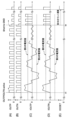
次に、上記構成における動作について図5の波形図を参照しつつ説明する。
第1のパルス信号幅変調信号が正相入力端子91から入力されると、第1のパルス信号幅変調信号は、正相パワートランジスタドライブ回路51、正相第1及び第2のパワートランジスタ1,2により電力増幅され正相出力端子93に正相出力信号OUTPとして出力される(図5(A)参照)。
第2のパルス信号幅変調信号が逆相入力端子92から入力されると、第2パルス信号幅変調信号は、逆相パワートランジスタドライブ回路52、逆相第1及び第2のパワートランジスタ3,4により電力増幅され逆相出力端子94に逆相出力信号OUTNとして出力される(図5(B)参照)。
Next, the operation of the above configuration will be described with reference to the waveform diagram of FIG.
When a first pulse signal width modulated signal is inputted from a positive
When the second pulse signal width modulated signal is inputted from the negative
正相出力信号OUTPは、第1の出力LCフィルタ81を介して、逆相出力信号OUTNは、第2の出力LCフィルタ82を介して、負荷37へ供給されて負荷37はBTL接続で駆動されることとなる。
回路起動時(図5において時刻t1)には、正相出力信号OUTP、逆相出力信号OUTNの立ち上がりにより第1及び第2の出力LCフィルタ81,82に起因する突入電流の発生により共振状態となるが、回路の動作状態は時間の経過に伴い徐々に定常状態となってゆく。
The positive phase output signal OUTP is supplied to the
When the circuit is started up (time t1 in FIG. 5), a resonant state occurs due to the generation of inrush current caused by the first and second output LC filters 81, 82 in response to the rising edges of the positive phase output signal OUTP and the negative phase output signal OUTN, but the operating state of the circuit gradually returns to a steady state over time.
すなわち、正相第1及び第2のパワートランジスタ1,2に流れる正相出力電流IOUTP、逆相第1及び第2のパワートランジスタ3,4に流れる逆相出力電流IOUTNは、回路起動後、しばらくの間は、正相出力信号OUTP、逆相出力信号OUTNの立ち上がり、立ち下がり近傍において第2の電流値を超える場合がある(図5(A)乃至図5(D)参照)。
その結果、第1のAND回路11により論理値Highに相当する信号が出力されると第1のDフリップフロップ15により、また、第2のAND回路12により論理値Highに相当する信号が出力されると第2のDフリップフロップ16により、それぞれ第1のパルス幅変調信号及び第2のパルス幅変調信号(図4(C)及び図4(D)参照)の1周期の間、論理値Highが保持される。
That is, the positive-phase output current IOUTP flowing through the first and second positive-
As a result, when the first AND
カウンタ回路18の第1のカウント周期は、計数動作(カウント動作)を繰り返し行う際の時間間隔であり、この第1のカウント周期時間は、第1及び第2の出力LCフィルタ81,82におけるLC共振周期よりも十分大きな時間に設定されている。そのため、第1のDフリップフロップ15、又は、第2のDフリップフロップ16からの論理値Highに対応する信号が、カウンタ回路18によって複数回計数されても、カウンタ回路18からカウントアップによる同時過電流検出信号が出力されることはない。
したがって、正相パワートランジスタドライブ回路51、逆相パワートランジスタドライブ回路52が、統合過電流検出信号OCDETによって動作停止されることはなく、回路起動後の回路動作を維持することができる。
The first count cycle of the
Therefore, the positive-phase power
一方、例えば、同時地絡が生じた場合(図5において時刻tn)、正相出力信号OUTP、逆相出力信号OUTは、電圧降下を生じ低電圧レベルとなる(図5(A)及び図5(B)参照)。
正相出力電流IOUTPと逆相出力電流IOUTNは、第1、第2のパルス幅変調信号PWMP、PWMNに、それぞれ同期するような出力状態となる(図5(C)及び図5(D)時刻tn以降参照)。
On the other hand, for example, when simultaneous ground faults occur (time tn in FIG. 5), the positive phase output signal OUTP and the negative phase output signal OUT experience a voltage drop and become low voltage levels (see FIGS. 5A and 5B).
The positive-phase output current IOUTP and the negative-phase output current IOUTN are in an output state synchronized with the first and second pulse-width modulation signals PWMP and PWMN, respectively (see FIG. 5C and FIG. 5D, after time tn).
ここで、第1、第2のパルス幅変調信号PWMP、PWMNの繰り返し周期は、カウンタ回路18の第1のカウント周期よりも小さく、しかも、この場合、正相出力電流IOUTPと逆相出力電流IOUTNは、第2の電流値を超える大きさであるため、出力の度毎に、第1のAND回路11からは、論理値Highに相当する同時天絡過電流検出信号が、第2のAND回路12からは、論理値Highに相当する同時地絡過電流検出信号が、それぞれ出力されることとなる。
Here, the repetition period of the first and second pulse width modulation signals PWMP, PWMN is smaller than the first count period of the
第1及び第2のDフリップフロップ15,16は、論理値Highに相当する信号が入力されると、第1のカウント周期の間、出力Qを論理値Highに保持する。
そして、第1及び第2のDフリップフロップ15,16のいずれかの論理値Highに相当する信号は、カウンタ回路18において第1のカウント周期の間、計数されることでカウンタ回路18からは、第1のカウント周期終了時に論理値Highに相当する同時過電流検出信号が出力される。この同時過電流検出信号に対応して5入力論理和回路19から論理値Highに相当する過電流検出信号OCDETが出力されることとなる(図5(E)参照)。
When a signal corresponding to a logical high value is input to the first and second D flip-
The signal corresponding to the logical value High of either the first or second D flip-
なお、第1のカウント周期中に同時天絡・当時地絡が発生した場合、その間、電流が流れてしまうが、ボンディングワイヤの溶断電流は、時間の関数となっており、通常、オーディオパワーアンプで使用するLCフィルタの回路定数を考慮して定められた第1のカウント周期においては溶断電流は十分大きいため、直ちにボンディングワイヤの溶断が生ずるような虞はない。
また、回路が定常状態にある場合には、LCフィルタ起因のリプル電流が流れるため、第2の電流値は想定されるリプル電流よりも大きめに設定すると好適である。
If a simultaneous power fault or simultaneous ground fault occurs during the first count period, current will flow during that time; however, the melting current of the bonding wire is a function of time, and the melting current is normally large enough in the first count period, which is determined taking into account the circuit constants of the LC filter used in audio power amplifiers, so there is no risk of the bonding wire melting immediately.
Furthermore, when the circuit is in a steady state, a ripple current due to the LC filter flows, so it is preferable to set the second current value to a value larger than the expected ripple current.
ボンディングワイヤの本数増加やボンディングパッド数の増加を抑えつつ、従来に比して、同時天絡、同時短絡時の過電流のより確実な抑圧が所望される電力増幅器に適用できる。 This technology can be applied to power amplifiers where more reliable suppression of overcurrents during simultaneous short circuits to the power supply or simultaneous short circuits is desired compared to conventional technology, while minimizing the need for an increase in the number of bonding wires or bonding pads.
1…正相第1のパワートランジスタ
2…正相第2のパワートランジスタ
3…逆相第1のパワートランジスタ
4…逆相第2のパワートランジスタ
5…正相第1のモニタトランジスタ
6…正相第2のモニタトランジスタ
7…逆相第1のモニタトランジスタ
8…逆相第2のモニタトランジスタ
51…正相パワートランジスタドライブ回路
52…逆相パワートランジスタドライブ回路
61…正相第1基準第1の過電流検出回路
62…正相第1基準第2の過電流検出回路
63…正相第2基準第1の過電流検出回路
62…正相第2基準第2の過電流検出回路
71…逆相第1基準第1の過電流検出回路
72…逆相第1基準第2の過電流検出回路
73…逆相第2基準第1の過電流検出回路
72…逆相第2基準第2の過電流検出回路
1...positive-phase
Claims (5)
前記過電流検出部は、前記正相信号増幅部と前記逆相信号増幅部における同時天絡の発生、又は、前記正相信号増幅部と前記逆相信号増幅部における同時地絡の発生により、前記正相信号増幅部と前記逆相信号増幅部のそれぞれにおける第2の電流値を超える過電流の発生を検出可能に構成されると共に、前記第1の電流値を超える過電流、又は、前記第2の電流値を超える過電流のいずれかが検出された場合に、前記正相信号増幅部及び前記逆相信号増幅部に対して統合過電流検出信号を出力し、
前記正相信号増幅部及び前記逆相信号増幅部は、前記統合過電流検出信号が出力された際に、それぞれ動作停止可能に構成されてなり、
前記正相信号増幅部は、正相パワートランジスタドライブ回路と、正相第1及び第2のパワートランジスタと、正相第1及び第2のモニタトランジスタとを有し、PチャンネルMOSFETの前記正相第1のパワートランジスタと、NチャンネルMOSFETの前記正相第2のパワートランジスタは、ドレインが相互に接続され、前記正相第1のパワートランジスタのソースには電源電圧が印可可能とされ、前記正相第2のパワートランジスタのソースはグランドに接続され、
前記正相第1及び第2のパワートランジスタは、外部から正相入力信号が入力される前記正相パワートランジスタドライブ回路のドライブ信号が、前記正相第1及び第2のパワートランジスタの各々のゲートに入力されることで駆動可能とされ、
PチャンネルMOSFETの前記正相第1のモニタトランジスタとNチャンネルMOSFETの前記正相第2のモニタトランジスタは、ドレインが相互に接続されると共に、前記正相第1及び第2のパワートランジスタのドレイン相互の接続点及び前記負荷の一端が接続される正相出力端子に接続され、
前記正相第1のモニタトランジスタのソースは、正相第1の検出抵抗器を介して前記電源電圧が印加可能とされ、
前記正相第2のモニタトランジスタのソースは、正相第2の検出抵抗器を介してグランドに接続され、
前記逆相信号増幅部は、逆相パワートランジスタドライブ回路と、逆相第1及び第2のパワートランジスタと、逆相第1及び第2のモニタトランジスタとを有し、PチャンネルMOSFETの前記逆相第1のパワートランジスタと、NチャンネルMOSFETの前記逆相第2のパワートランジスタは、ドレインが相互に接続され、前記逆相第1のパワートランジスタのソースには前記電源電圧が印可可能とされ、前記逆相第2のパワートランジスタのソースはグランドに接続され、
前記逆相第1及び第2のパワートランジスタは、外部から逆相入力信号が入力される前記逆相パワートランジスタドライブ回路のドライブ信号が、前記逆相第1及び第2のパワートランジスタの各々のゲートに入力されることで駆動可能とされ、
PチャンネルMOSFETの前記逆相第1のモニタトランジスタとNチャンネルMOSFETの前記逆相第2のモニタトランジスタは、ドレインが相互に接続されると共に、前記逆相第1及び第2のパワートランジスタのドレイン相互の接続点及び前記負荷の他端が接続される逆相出力端子に接続され、
前記正相出力端子と前記逆相出力端子の間には、前記負荷が接続され、
前記逆相第1のモニタトランジスタのソースは、逆相第1の検出抵抗器を介して前記電源電圧が印加可能とされ、
前記逆相第2のモニタトランジスタのソースは、逆相第2の検出抵抗器を介してグランドに接続され、
前記過電流検出部は、正相第1基準第1及び第2の過電流検出回路と、逆相第1基準第1及び第2の過電流検出回路と、正相第2基準第1及び第2の過電流検出回路と、逆相第2基準第1及び第2の過電流検出回路とを有し、
前記正相第1のモニタトランジスタのソースと前記正相第1の検出抵抗器との接続点は、前記正相第1基準第1の過電流検出回路及び前記正相第2基準第1の過電流検出回路の入力段に接続され、
前記正相第2のモニタトランジスタのソースと前記正相第2の検出抵抗器との接続点は、前記正相第1基準第2の過電流検出回路及び前記正相第2基準第2の過電流検出回路の入力段に接続され、
前記逆相第1のモニタトランジスタのソースと前記逆相第1の検出抵抗器との接続点は、前記逆相第1基準第1の過電流検出回路及び前記逆相第2基準第1の過電流検出回路の入力段に接続され、
前記逆相第2のモニタトランジスタのソースと前記逆相第2の検出抵抗器との接続点は、前記逆相第1基準第2の過電流検出回路及び前記逆相第2基準第2の過電流検出回路の入力段に接続され、
前記正相出力端子と逆相出力端子における同時地絡の発生により、前記正相第1のモニタトランジスタにより検出された前記正相第1のパワートランジスタの電流が、前記正相第2基準第1の過電流検出回路によって前記第2の電流値を超える過電流と判定され、前記逆相第1のモニタトランジスタにより検出された前記逆相第1のパワートランジスタの電流が、前記逆相第2基準第1の過電流検出回路によって前記第2の電流値を超える過電流と判定された場合に、前記過電流検出部による前記正相信号増幅部及び前記逆相信号増幅部に対する前記統合過電流検出信号が出力され、
前記正相出力端子と逆相出力端子における同時天絡の発生により、前記正相第2のモニタトランジスタにより検出された前記正相第2のパワートランジスタの電流が、前記正相第2基準第2の過電流検出回路によって前記第2の電流値を超える過電流と判定され、前記逆相第2のモニタトランジスタにより検出された前記逆相第2のパワートランジスタの電流が、前記逆相第2基準第2の過電流検出回路によって前記第2の電流値を超える過電流と判定された場合に、前記過電流検出部による前記正相信号増幅部及び前記逆相信号増幅部に対する前記統合過電流検出信号が出力されるよう構成されてなることを特徴とする電力増幅器。 A power amplifier comprising: a positive-phase signal amplifier section for amplifying a positive-phase input signal; and a negative-phase signal amplifier section for amplifying a negative-phase input signal, wherein an output of the positive-phase signal amplifier section and an output of the negative-phase signal amplifier section can be supplied to a load via a BTL connection; and an overcurrent detection section configured to detect an occurrence of an overcurrent exceeding a first current value in the positive-phase signal amplifier section and an occurrence of an overcurrent exceeding the first current value in the negative-phase signal amplifier section,
the overcurrent detection unit is configured to be able to detect an occurrence of an overcurrent exceeding a second current value in each of the positive-phase signal amplifier unit and the negative-phase signal amplifier unit due to a simultaneous power short in the positive-phase signal amplifier unit and the negative-phase signal amplifier unit, or a simultaneous ground short in the positive-phase signal amplifier unit and the negative-phase signal amplifier unit, and outputs an integrated overcurrent detection signal to the positive-phase signal amplifier unit and the negative-phase signal amplifier unit when either an overcurrent exceeding the first current value or an overcurrent exceeding the second current value is detected;
the positive-phase signal amplifier and the negative-phase signal amplifier are each configured to be stopped when the integrated overcurrent detection signal is output,
the positive phase signal amplifier section has a positive phase power transistor drive circuit, positive phase first and second power transistors, and positive phase first and second monitor transistors, the positive phase first power transistor being a P-channel MOSFET and the positive phase second power transistor being an N-channel MOSFET, the drains of which are connected to each other, a power supply voltage can be applied to the source of the positive phase first power transistor, and the source of the positive phase second power transistor is connected to ground,
the first and second positive phase power transistors can be driven by a drive signal of the positive phase power transistor drive circuit to which a positive phase input signal is input from an external source, being input to the gates of the first and second positive phase power transistors,
the positive phase first monitor transistor which is a P-channel MOSFET and the positive phase second monitor transistor which is an N-channel MOSFET have drains which are connected to each other and are also connected to a positive phase output terminal to which a connection point between the drains of the positive phase first and second power transistors and one end of the load are connected;
the power supply voltage can be applied to a source of the first positive phase monitor transistor via a first positive phase detection resistor;
a source of the second positive phase monitor transistor is connected to ground via a second positive phase detection resistor;
the negative-phase signal amplifier section has a negative-phase power transistor drive circuit, negative-phase first and second power transistors, and negative-phase first and second monitor transistors, the drains of the negative-phase first power transistor which is a P-channel MOSFET and the negative-phase second power transistor which is an N-channel MOSFET are connected to each other, the power supply voltage can be applied to the source of the negative-phase first power transistor, and the source of the negative-phase second power transistor is connected to ground,
the first and second negative-phase power transistors can be driven by a drive signal of the negative-phase power transistor drive circuit to which an external negative-phase input signal is input, being input to each gate of the first and second negative-phase power transistors;
the drains of the negative-phase first monitor transistor which is a P-channel MOSFET and the drains of the negative-phase second monitor transistor which is an N-channel MOSFET are connected to each other and to a negative-phase output terminal to which a connection point between the drains of the negative-phase first and second power transistors and the other end of the load are connected;
the load is connected between the positive phase output terminal and the negative phase output terminal;
the power supply voltage can be applied to a source of the negative-phase first monitor transistor via a negative-phase first detection resistor;
a source of the inverted second monitor transistor is connected to ground via an inverted second sense resistor;
the overcurrent detection unit includes positive-phase first-reference first and second overcurrent detection circuits, negative-phase first-reference first and second overcurrent detection circuits, positive-phase second-reference first and second overcurrent detection circuits, and negative-phase second-reference first and second overcurrent detection circuits;
a connection point between a source of the positive-phase first monitor transistor and the positive-phase first detection resistor is connected to an input stage of the positive-phase first reference first overcurrent detection circuit and the positive-phase second reference first overcurrent detection circuit;
a connection point between a source of the positive-phase second monitor transistor and the positive-phase second detection resistor is connected to an input stage of the positive-phase first reference second overcurrent detection circuit and the positive-phase second reference second overcurrent detection circuit;
a connection point between a source of the negative-phase first monitor transistor and the negative-phase first detection resistor is connected to an input stage of the negative-phase first reference first overcurrent detection circuit and the negative-phase second reference first overcurrent detection circuit;
a connection point between a source of the negative-phase second monitor transistor and the negative-phase second detection resistor is connected to an input stage of the negative-phase first reference second overcurrent detection circuit and the negative-phase second reference second overcurrent detection circuit;
when a simultaneous ground fault occurs at the positive-phase output terminal and the negative-phase output terminal, the current of the positive-phase first power transistor detected by the positive-phase first monitor transistor is determined to be an overcurrent exceeding the second current value by the positive-phase second reference first overcurrent detection circuit, and the current of the negative-phase first power transistor detected by the negative-phase first monitor transistor is determined to be an overcurrent exceeding the second current value by the negative-phase second reference first overcurrent detection circuit, the overcurrent detection unit outputs the integrated overcurrent detection signal to the positive-phase signal amplifier unit and the negative-phase signal amplifier unit,
a current of the second positive-phase power transistor detected by the second positive-phase monitor transistor being determined to be an overcurrent exceeding the second current value by the second positive-phase reference second overcurrent detection circuit, and a current of the second negative-phase power transistor detected by the second negative-phase monitor transistor being determined to be an overcurrent exceeding the second current value by the second negative-phase reference second overcurrent detection circuit due to a simultaneous short-to-power occurrence at the positive-phase output terminal and the negative-phase output terminal,
前記過電流検出部は、前記正相信号増幅部と前記逆相信号増幅部における同時天絡の発生により第2の電流値を超える過電流の発生が検出された際に、論理値Highに相当する同時天絡過電流検出信号を生成すると共に、当該同時天絡過電流検出信号を前記第1のパルス幅変調信号及び第2のパルス幅変調信号の1周期分保持する第1のDフリップフロップが設けられる一方、
前記正相信号増幅部と前記逆相信号増幅部における同時地絡の発生により第2の電流値を超える過電流の発生が検出された際に、論理値Highに相当する同時地絡過電流検出信号を生成すると共に、当該同時地絡過電流検出信号を前記パルス幅変調信号の1周期分保持する第2のDフリップフロップが設けられ、
前記第1又は第2のDフリップフロップからの論理値Highに相当する出力信号を第1のカウント周期の間、計数後に論理値Highに相当する同時過電流検出信号として出力するカウンタ回路が設けられ、前記カウンタ回路が前記同時過電流検出信号を出力した場合に、前記統合過電流検出信号を出力可能に構成されてなることを特徴とする請求項3記載の電力増幅器。 a first LC filter is provided between the positive-phase signal amplifier and the load, and a second LC filter is provided between the negative-phase signal amplifier and the load,
the overcurrent detection unit generates a simultaneous power fault overcurrent detection signal corresponding to a logical value High when an overcurrent exceeding a second current value is detected due to a simultaneous power fault in the positive-phase signal amplifier unit and the negative-phase signal amplifier unit, and includes a first D flip-flop that holds the simultaneous power fault overcurrent detection signal for one period of the first pulse-width modulated signal and the second pulse-width modulated signal;
a second D flip-flop is provided for generating a simultaneous earth fault overcurrent detection signal corresponding to a logical value High when an occurrence of an overcurrent exceeding a second current value is detected due to the occurrence of simultaneous earth faults in the positive phase signal amplifier and the negative phase signal amplifier, and for holding the simultaneous earth fault overcurrent detection signal for one period of the pulse width modulation signal;
The power amplifier according to claim 3, further comprising a counter circuit that outputs an output signal corresponding to a logical High value from the first or second D flip-flop as a simultaneous overcurrent detection signal corresponding to a logical High value after counting during a first count period, and is configured to be able to output the integrated overcurrent detection signal when the counter circuit outputs the simultaneous overcurrent detection signal.
Priority Applications (1)
| Application Number | Priority Date | Filing Date | Title |
|---|---|---|---|
| JP2020209599A JP7588937B2 (en) | 2020-12-17 | 2020-12-17 | Power Amplifiers |
Applications Claiming Priority (1)
| Application Number | Priority Date | Filing Date | Title |
|---|---|---|---|
| JP2020209599A JP7588937B2 (en) | 2020-12-17 | 2020-12-17 | Power Amplifiers |
Publications (2)
| Publication Number | Publication Date |
|---|---|
| JP2022096475A JP2022096475A (en) | 2022-06-29 |
| JP7588937B2 true JP7588937B2 (en) | 2024-11-25 |
Family
ID=82163694
Family Applications (1)
| Application Number | Title | Priority Date | Filing Date |
|---|---|---|---|
| JP2020209599A Active JP7588937B2 (en) | 2020-12-17 | 2020-12-17 | Power Amplifiers |
Country Status (1)
| Country | Link |
|---|---|
| JP (1) | JP7588937B2 (en) |
Citations (4)
| Publication number | Priority date | Publication date | Assignee | Title |
|---|---|---|---|---|
| JP2002171140A (en) | 2000-12-01 | 2002-06-14 | Mitsubishi Electric Corp | Audio signal amplification output circuit |
| JP2007325236A (en) | 2006-06-05 | 2007-12-13 | Yamaha Corp | Class-d amplifier and overcurrent protecting method thereof |
| JP2012235403A (en) | 2011-05-09 | 2012-11-29 | New Japan Radio Co Ltd | Capacitive speaker driving circuit |
| JP2020065120A (en) | 2018-10-15 | 2020-04-23 | 新日本無線株式会社 | Class D amplifier circuit |
Family Cites Families (1)
| Publication number | Priority date | Publication date | Assignee | Title |
|---|---|---|---|---|
| JP2565818B2 (en) * | 1992-02-19 | 1996-12-18 | ローム株式会社 | BTL amplifier protection circuit and audio device |
-
2020
- 2020-12-17 JP JP2020209599A patent/JP7588937B2/en active Active
Patent Citations (4)
| Publication number | Priority date | Publication date | Assignee | Title |
|---|---|---|---|---|
| JP2002171140A (en) | 2000-12-01 | 2002-06-14 | Mitsubishi Electric Corp | Audio signal amplification output circuit |
| JP2007325236A (en) | 2006-06-05 | 2007-12-13 | Yamaha Corp | Class-d amplifier and overcurrent protecting method thereof |
| JP2012235403A (en) | 2011-05-09 | 2012-11-29 | New Japan Radio Co Ltd | Capacitive speaker driving circuit |
| JP2020065120A (en) | 2018-10-15 | 2020-04-23 | 新日本無線株式会社 | Class D amplifier circuit |
Also Published As
| Publication number | Publication date |
|---|---|
| JP2022096475A (en) | 2022-06-29 |
Similar Documents
| Publication | Publication Date | Title |
|---|---|---|
| US8284953B2 (en) | Circuit and method of reducing pop-up noise in a digital amplifier | |
| US8134400B2 (en) | Semiconductor circuit | |
| US10367459B2 (en) | Class-D amplifier circuit | |
| US7586369B2 (en) | Pulse modulation type electric power amplifier | |
| US7940138B2 (en) | Electrostatic discharge protection oscillation circuit in LSI | |
| JP5160320B2 (en) | Switching drive circuit | |
| US9160290B2 (en) | Class D amplifier and control method | |
| WO2004010575A1 (en) | Power amplifier | |
| JP2007082036A (en) | Semiconductor integrated circuit device, power supply apparatus, and electric apparatus | |
| US7982522B2 (en) | Semiconductor integrated circuit for realizing an amplifier having ringing reduction circuitry | |
| JP7588937B2 (en) | Power Amplifiers | |
| US7564275B2 (en) | Switching circuit and a method of driving a load | |
| JP5094431B2 (en) | Power amplifier circuit | |
| US8525559B2 (en) | Non-overlap circuit | |
| JP4835665B2 (en) | RINGING REDUCTION CIRCUIT AND SEMICONDUCTOR INTEGRATED CIRCUIT HAVING THE RINGING REDUCTION CIRCUIT | |
| JP2004056254A (en) | Power amplifier device | |
| JP7718823B2 (en) | Class D amplifier circuit | |
| JP4222389B2 (en) | RINGING REDUCTION CIRCUIT AND SEMICONDUCTOR INTEGRATED CIRCUIT HAVING THE RINGING REDUCTION CIRCUIT | |
| CN222147149U (en) | An inverter output protection circuit | |
| US7388431B2 (en) | Switching amplifier and control method thereof | |
| JP2024118719A (en) | Class D amplifier circuit | |
| JP3951917B2 (en) | Pulse width modulation amplifier | |
| CN113302570B (en) | Interface circuit | |
| JPH01119773A (en) | inverter circuit | |
| CN119448998A (en) | Load driving circuit and control method of load driving circuit |
Legal Events
| Date | Code | Title | Description |
|---|---|---|---|
| A621 | Written request for application examination |
Free format text: JAPANESE INTERMEDIATE CODE: A621 Effective date: 20231110 |
|
| A977 | Report on retrieval |
Free format text: JAPANESE INTERMEDIATE CODE: A971007 Effective date: 20240725 |
|
| A131 | Notification of reasons for refusal |
Free format text: JAPANESE INTERMEDIATE CODE: A131 Effective date: 20240730 |
|
| A601 | Written request for extension of time |
Free format text: JAPANESE INTERMEDIATE CODE: A601 Effective date: 20240925 |
|
| A521 | Request for written amendment filed |
Free format text: JAPANESE INTERMEDIATE CODE: A523 Effective date: 20241017 |
|
| TRDD | Decision of grant or rejection written | ||
| A01 | Written decision to grant a patent or to grant a registration (utility model) |
Free format text: JAPANESE INTERMEDIATE CODE: A01 Effective date: 20241112 |
|
| A61 | First payment of annual fees (during grant procedure) |
Free format text: JAPANESE INTERMEDIATE CODE: A61 Effective date: 20241112 |
|
| R150 | Certificate of patent or registration of utility model |
Ref document number: 7588937 Country of ref document: JP Free format text: JAPANESE INTERMEDIATE CODE: R150 |