JP7586825B2 - Semiconductor Device - Google Patents
Semiconductor Device Download PDFInfo
- Publication number
- JP7586825B2 JP7586825B2 JP2021546059A JP2021546059A JP7586825B2 JP 7586825 B2 JP7586825 B2 JP 7586825B2 JP 2021546059 A JP2021546059 A JP 2021546059A JP 2021546059 A JP2021546059 A JP 2021546059A JP 7586825 B2 JP7586825 B2 JP 7586825B2
- Authority
- JP
- Japan
- Prior art keywords
- oxide
- insulator
- conductor
- region
- transistor
- Prior art date
- Legal status (The legal status is an assumption and is not a legal conclusion. Google has not performed a legal analysis and makes no representation as to the accuracy of the status listed.)
- Active
Links
Images


Classifications
-
- H—ELECTRICITY
- H10—SEMICONDUCTOR DEVICES; ELECTRIC SOLID-STATE DEVICES NOT OTHERWISE PROVIDED FOR
- H10D—INORGANIC ELECTRIC SEMICONDUCTOR DEVICES
- H10D30/00—Field-effect transistors [FET]
- H10D30/60—Insulated-gate field-effect transistors [IGFET]
- H10D30/67—Thin-film transistors [TFT]
- H10D30/674—Thin-film transistors [TFT] characterised by the active materials
- H10D30/6755—Oxide semiconductors, e.g. zinc oxide, copper aluminium oxide or cadmium stannate
-
- H—ELECTRICITY
- H10—SEMICONDUCTOR DEVICES; ELECTRIC SOLID-STATE DEVICES NOT OTHERWISE PROVIDED FOR
- H10B—ELECTRONIC MEMORY DEVICES
- H10B12/00—Dynamic random access memory [DRAM] devices
-
- H—ELECTRICITY
- H10—SEMICONDUCTOR DEVICES; ELECTRIC SOLID-STATE DEVICES NOT OTHERWISE PROVIDED FOR
- H10B—ELECTRONIC MEMORY DEVICES
- H10B41/00—Electrically erasable-and-programmable ROM [EEPROM] devices comprising floating gates
- H10B41/70—Electrically erasable-and-programmable ROM [EEPROM] devices comprising floating gates the floating gate being an electrode shared by two or more components
-
- H—ELECTRICITY
- H10—SEMICONDUCTOR DEVICES; ELECTRIC SOLID-STATE DEVICES NOT OTHERWISE PROVIDED FOR
- H10D—INORGANIC ELECTRIC SEMICONDUCTOR DEVICES
- H10D30/00—Field-effect transistors [FET]
- H10D30/60—Insulated-gate field-effect transistors [IGFET]
- H10D30/67—Thin-film transistors [TFT]
- H10D30/6704—Thin-film transistors [TFT] having supplementary regions or layers in the thin films or in the insulated bulk substrates for controlling properties of the device
- H10D30/6713—Thin-film transistors [TFT] having supplementary regions or layers in the thin films or in the insulated bulk substrates for controlling properties of the device characterised by the properties of the source or drain regions, e.g. compositions or sectional shapes
-
- H—ELECTRICITY
- H10—SEMICONDUCTOR DEVICES; ELECTRIC SOLID-STATE DEVICES NOT OTHERWISE PROVIDED FOR
- H10D—INORGANIC ELECTRIC SEMICONDUCTOR DEVICES
- H10D30/00—Field-effect transistors [FET]
- H10D30/60—Insulated-gate field-effect transistors [IGFET]
- H10D30/67—Thin-film transistors [TFT]
- H10D30/6729—Thin-film transistors [TFT] characterised by the electrodes
- H10D30/673—Thin-film transistors [TFT] characterised by the electrodes characterised by the shapes, relative sizes or dispositions of the gate electrodes
- H10D30/6733—Multi-gate TFTs
- H10D30/6734—Multi-gate TFTs having gate electrodes arranged on both top and bottom sides of the channel, e.g. dual-gate TFTs
-
- H—ELECTRICITY
- H10—SEMICONDUCTOR DEVICES; ELECTRIC SOLID-STATE DEVICES NOT OTHERWISE PROVIDED FOR
- H10D—INORGANIC ELECTRIC SEMICONDUCTOR DEVICES
- H10D30/00—Field-effect transistors [FET]
- H10D30/60—Insulated-gate field-effect transistors [IGFET]
- H10D30/68—Floating-gate IGFETs
-
- H—ELECTRICITY
- H10—SEMICONDUCTOR DEVICES; ELECTRIC SOLID-STATE DEVICES NOT OTHERWISE PROVIDED FOR
- H10D—INORGANIC ELECTRIC SEMICONDUCTOR DEVICES
- H10D30/00—Field-effect transistors [FET]
- H10D30/60—Insulated-gate field-effect transistors [IGFET]
- H10D30/69—IGFETs having charge trapping gate insulators, e.g. MNOS transistors
-
- H—ELECTRICITY
- H10—SEMICONDUCTOR DEVICES; ELECTRIC SOLID-STATE DEVICES NOT OTHERWISE PROVIDED FOR
- H10D—INORGANIC ELECTRIC SEMICONDUCTOR DEVICES
- H10D64/00—Electrodes of devices having potential barriers
- H10D64/01—Manufacture or treatment
- H10D64/011—Manufacture or treatment of electrodes ohmically coupled to a semiconductor
-
- H—ELECTRICITY
- H10—SEMICONDUCTOR DEVICES; ELECTRIC SOLID-STATE DEVICES NOT OTHERWISE PROVIDED FOR
- H10D—INORGANIC ELECTRIC SEMICONDUCTOR DEVICES
- H10D84/00—Integrated devices formed in or on semiconductor substrates that comprise only semiconducting layers, e.g. on Si wafers or on GaAs-on-Si wafers
- H10D84/01—Manufacture or treatment
- H10D84/0123—Integrating together multiple components covered by H10D12/00 or H10D30/00, e.g. integrating multiple IGBTs
- H10D84/0126—Integrating together multiple components covered by H10D12/00 or H10D30/00, e.g. integrating multiple IGBTs the components including insulated gates, e.g. IGFETs
-
- H—ELECTRICITY
- H10—SEMICONDUCTOR DEVICES; ELECTRIC SOLID-STATE DEVICES NOT OTHERWISE PROVIDED FOR
- H10D—INORGANIC ELECTRIC SEMICONDUCTOR DEVICES
- H10D84/00—Integrated devices formed in or on semiconductor substrates that comprise only semiconducting layers, e.g. on Si wafers or on GaAs-on-Si wafers
- H10D84/01—Manufacture or treatment
- H10D84/02—Manufacture or treatment characterised by using material-based technologies
- H10D84/03—Manufacture or treatment characterised by using material-based technologies using Group IV technology, e.g. silicon technology or silicon-carbide [SiC] technology
- H10D84/038—Manufacture or treatment characterised by using material-based technologies using Group IV technology, e.g. silicon technology or silicon-carbide [SiC] technology using silicon technology, e.g. SiGe
-
- H—ELECTRICITY
- H10—SEMICONDUCTOR DEVICES; ELECTRIC SOLID-STATE DEVICES NOT OTHERWISE PROVIDED FOR
- H10D—INORGANIC ELECTRIC SEMICONDUCTOR DEVICES
- H10D87/00—Integrated devices comprising both bulk components and either SOI or SOS components on the same substrate
Landscapes
- Thin Film Transistor (AREA)
- Semiconductor Memories (AREA)
- Metal-Oxide And Bipolar Metal-Oxide Semiconductor Integrated Circuits (AREA)
Description
本発明の一態様は、トランジスタ、半導体装置、および電子機器に関する。また、本発明の一態様は、トランジスタ、および半導体装置の作製方法に関する。また、本発明の一態様は、半導体ウエハ、およびモジュールに関する。1. Field of the Invention [0003] One embodiment of the present invention relates to a transistor, a semiconductor device, and an electronic device. Another embodiment of the present invention relates to a method for manufacturing the transistor and the semiconductor device. Another embodiment of the present invention relates to a semiconductor wafer and a module.
なお、本明細書等において半導体装置とは、半導体特性を利用することで機能し得る装置全般を指す。トランジスタなどの半導体素子をはじめ、半導体回路、演算装置、記憶装置は、半導体装置の一態様である。表示装置(液晶表示装置、発光表示装置など)、投影装置、照明装置、電気光学装置、蓄電装置、記憶装置、半導体回路、撮像装置、電子機器などは、半導体装置を有すると言える場合がある。In this specification and the like, a semiconductor device refers to any device that can function by utilizing semiconductor characteristics. Semiconductor elements such as transistors, semiconductor circuits, arithmetic devices, and memory devices are one embodiment of semiconductor devices. Display devices (such as liquid crystal display devices and light-emitting display devices), projection devices, lighting devices, electro-optical devices, power storage devices, memory devices, semiconductor circuits, imaging devices, electronic devices, and the like may be said to include semiconductor devices.
なお、本発明の一態様は、上記の技術分野に限定されない。本明細書等で開示する発明の一態様は、物、方法、または、製造方法に関するものである。また、本発明の一態様は、プロセス、マシン、マニュファクチャ、または、組成物(コンポジション・オブ・マター)に関するものである。Note that one embodiment of the present invention is not limited to the above technical field. One embodiment of the present invention disclosed in the present specification and the like relates to an object, a method, or a manufacturing method. In addition, one embodiment of the present invention relates to a process, a machine, a manufacture, or a composition of matter.
近年、半導体装置の開発が進められ、LSIやCPUやメモリが主に用いられている。CPUは、半導体ウエハから切り離された半導体集積回路(少なくともトランジスタ及びメモリ)を有し、接続端子である電極が形成された半導体素子の集合体である。In recent years, the development of semiconductor devices has progressed, and LSIs, CPUs, and memories are mainly used. A CPU is a collection of semiconductor elements having a semiconductor integrated circuit (at least a transistor and a memory) separated from a semiconductor wafer and having electrodes formed as connection terminals.
LSIやCPUやメモリなどの半導体回路(ICチップ)は、回路基板、例えばプリント配線板に実装され、様々な電子機器の部品の一つとして用いられる。2. Description of the Related Art Semiconductor circuits (IC chips) such as LSIs, CPUs, and memories are mounted on circuit boards, such as printed wiring boards, and are used as components of various electronic devices.
また、絶縁表面を有する基板上に形成された半導体薄膜を用いてトランジスタを構成する技術が注目されている。該トランジスタは集積回路(IC)や画像表示装置(単に表示装置とも表記する)のような電子デバイスに広く応用されている。トランジスタに適用可能な半導体薄膜としてシリコン系半導体材料が広く知られているが、その他の材料として酸化物半導体が注目されている。In addition, a technology for constructing a transistor using a semiconductor thin film formed on a substrate having an insulating surface has been attracting attention. The transistor is widely applied to electronic devices such as integrated circuits (ICs) and image display devices (also simply referred to as display devices). Silicon-based semiconductor materials are widely known as semiconductor thin films applicable to transistors, but oxide semiconductors have also been attracting attention as other materials.
また、酸化物半導体を用いたトランジスタは、非導通状態において極めてリーク電流が小さいことが知られている。例えば、酸化物半導体を用いたトランジスタのリーク電流が低いという特性を応用した低消費電力のCPUなどが開示されている(特許文献1参照。)。また、例えば、酸化物半導体を用いたトランジスタのリーク電流が低いという特性を応用して、長期にわたり記憶内容を保持することができる記憶装置などが、開示されている(特許文献2参照。)。It is also known that a transistor using an oxide semiconductor has an extremely low leakage current in a non-conducting state. For example, a CPU with low power consumption that utilizes the low leakage current characteristic of a transistor using an oxide semiconductor has been disclosed (see Patent Document 1). In addition, a memory device that can retain stored data for a long period of time by utilizing the low leakage current characteristic of a transistor using an oxide semiconductor has been disclosed (see Patent Document 2).
また、近年では電子機器の小型化、軽量化に伴い、集積回路のさらなる高密度化への要求が高まっている。また、集積回路を含む半導体装置の生産性の向上が求められている。Furthermore, in recent years, with the trend toward smaller and lighter electronic devices, there is an increasing demand for higher density integrated circuits, and there is also a demand for improved productivity in the manufacture of semiconductor devices including integrated circuits.
上記問題を鑑み、本発明の一態様は、トランジスタ特性のばらつきが少ない半導体装置を提供することを課題の一つとする。また、本発明の一態様は、信頼性が良好な半導体装置を提供することを課題の一つとする。また、本発明の一態様は、良好な電気特性を有する半導体装置を提供することを課題の一つとする。また、本発明の一態様は、オン電流が大きい半導体装置を提供することを課題の一つとする。また、本発明の一態様は、微細化または高集積化が可能な半導体装置を提供することを課題の一つとする。また、本発明の一態様は、低消費電力の半導体装置を提供することを課題の一つとする。In view of the above problems, an object of one embodiment of the present invention is to provide a semiconductor device with little variation in transistor characteristics. Another object of one embodiment of the present invention is to provide a semiconductor device with good reliability. Another object of one embodiment of the present invention is to provide a semiconductor device having good electrical characteristics. Another object of one embodiment of the present invention is to provide a semiconductor device with large on-state current. Another object of one embodiment of the present invention is to provide a semiconductor device that can be miniaturized or highly integrated. Another object of one embodiment of the present invention is to provide a semiconductor device with low power consumption.
なお、これらの課題の記載は、他の課題の存在を妨げるものではない。なお、本発明の一態様は、これらの課題の全てを解決する必要はないものとする。なお、これら以外の課題は、明細書、図面、請求項などの記載から、自ずと明らかとなるものであり、明細書、図面、請求項などの記載から、これら以外の課題を抽出することが可能である。Note that the description of these problems does not preclude the existence of other problems. Note that one embodiment of the present invention does not necessarily solve all of these problems. Note that problems other than these will become apparent from the description of the specification, drawings, claims, etc., and it is possible to extract problems other than these from the description of the specification, drawings, claims, etc.
本発明の一態様は、第1の絶縁体と、第1の絶縁体上の第1の酸化物と、第1の酸化物上の第2の酸化物と、第2の酸化物上の、第1の導電体、第2の導電体、第3の酸化物、第4の酸化物、および第2の絶縁体と、第1の導電体上、第2の導電体上、第3の酸化物上、および第4の酸化物上の、第3の絶縁体と、第2の絶縁体上の、第4の絶縁体と、第4の絶縁体上の、第3の導電体と、を有する半導体装置である。第2の絶縁体は、第1の導電体と、第2の導電体との間に位置し、第3の酸化物は、第1の導電体と、第2の絶縁体との間に位置し、第4の酸化物は、第2の導電体と、第2の絶縁体との間に位置する。第2の酸化物は、第1の領域、第2の領域、第3の領域、第4の領域、および第5の領域を有する。第1の領域は、第1の導電体と接する領域を有し、第2の領域は、第3の酸化物と接する領域を有し、第3の領域は、第3の導電体と重畳する領域を有し、第4の領域は、第4の酸化物と接する領域を有し、第5の領域は、第2の導電体と接する領域を有する。第2の領域の、第1の領域と第3の領域との間の長さは、3nm以上8nm以下であり、第4の領域の、第3の領域と第5の領域との間の長さは、3nm以上8nm以下であり、第3の領域の、第2の領域と第4の領域との間の長さは、5nm以上40nm以下である。第2の領域、および第4の領域のキャリア濃度のそれぞれは、第3の領域のキャリア濃度よりも高く、第1の領域、および第5の領域のキャリア濃度は、それぞれ第2の領域、および第4の領域のキャリア濃度よりも高い。One aspect of the present invention is a semiconductor device having a first insulator, a first oxide on the first insulator, a second oxide on the first oxide, a first conductor, a second conductor, a third oxide, a fourth oxide, and a second insulator on the second oxide, a third insulator on the first conductor, the second conductor, the third oxide, and the fourth oxide, a fourth insulator on the second insulator, and a third conductor on the fourth insulator. The second insulator is located between the first conductor and the second conductor, the third oxide is located between the first conductor and the second insulator, and the fourth oxide is located between the second conductor and the second insulator. The second oxide has a first region, a second region, a third region, a fourth region, and a fifth region. The first region has a region in contact with the first conductor, the second region has a region in contact with the third oxide, the third region has a region overlapping with the third conductor, the fourth region has a region in contact with the fourth oxide, and the fifth region has a region in contact with the second conductor. The length between the first region and the third region in the second region is 3 nm or more and 8 nm or less, the length between the third region and the fifth region in the fourth region is 3 nm or more and 8 nm or less, and the length between the second region and the fourth region in the third region is 5 nm or more and 40 nm or less. The carrier concentrations of the second region and the fourth region are each higher than that of the third region, and the carrier concentrations of the first region and the fifth region are each higher than that of the second region and the fourth region.
また、本発明の一態様は、第1の絶縁体と、第1の絶縁体上の第1の酸化物と、第1の酸化物上の第2の酸化物と、第2の酸化物上の、第1の導電体、第2の導電体、第3の酸化物、第4の酸化物、および第2の絶縁体と、第1の導電体上、第2の導電体上、第3の酸化物上、および第4の酸化物上の、第3の絶縁体と、第2の絶縁体上の、第4の絶縁体と、第4の絶縁体上の、第3の導電体と、を有する半導体装置である。第2の絶縁体は、第1の導電体と、第2の導電体との間に位置し、第3の酸化物は、第1の導電体と、第2の絶縁体との間に位置し、第4の酸化物は、第2の導電体と、第2の絶縁体との間に位置する。第1の導電体と第2の絶縁体との間の、第3の酸化物の膜厚は、3nm以上8nm以下であり、第2の導電体と第2の絶縁体との間の、第4の酸化物の膜厚は、3nm以上8nm以下であり、第2の酸化物と重なる領域の、第3の導電体の底面の長さは、5nm以上40nm以下である。Another embodiment of the present invention is a semiconductor device including a first insulator, a first oxide on the first insulator, a second oxide on the first oxide, a first conductor, a second conductor, a third oxide, a fourth oxide, and a second insulator on the second oxide, a third insulator on the first conductor, the second conductor, the third oxide, and the fourth oxide, a fourth insulator on the second insulator, and a third conductor on the fourth insulator, wherein the second insulator is located between the first conductor and the second conductor, the third oxide is located between the first conductor and the second insulator, and the fourth oxide is located between the second conductor and the second insulator. The thickness of the third oxide between the first conductor and the second insulator is 3 nm or more and 8 nm or less, the thickness of the fourth oxide between the second conductor and the second insulator is 3 nm or more and 8 nm or less, and the length of the bottom surface of the third conductor in the region overlapping with the second oxide is 5 nm or more and 40 nm or less.
上記半導体装置において、第1の導電体、および第2の導電体のそれぞれは、タンタルを有し、第3の酸化物、および第4の酸化物のそれぞれは、タンタルと、酸素と、を有する、ことが好ましい。In the above semiconductor device, it is preferable that the first conductor and the second conductor each contain tantalum, and the third oxide and the fourth oxide each contain tantalum and oxygen.
また、上記半導体装置において、第2の絶縁体は、シリコンと、酸素と、を有し、第4の絶縁体は、ハフニウムと、酸素と、を有する、ことが好ましい。In the above semiconductor device, it is preferable that the second insulator contains silicon and oxygen, and the fourth insulator contains hafnium and oxygen.
また、上記半導体装置において、第2の酸化物は、インジウムと、元素M(Mはガリウム、アルミニウム、イットリウム、および錫のいずれか一または複数)と、亜鉛と、を有することが好ましい。In the above semiconductor device, the second oxide preferably contains indium, an element M (M is one or more of gallium, aluminum, yttrium, and tin), and zinc.
また、上記半導体装置において、第1の酸化物、および第2の酸化物は、島状にパターニングされていることが好ましい。In the above semiconductor device, the first oxide and the second oxide are preferably patterned into islands.
本発明の一態様により、トランジスタ特性のばらつきが少ない半導体装置を提供することができる。また、本発明の一態様により、信頼性が良好な半導体装置を提供することができる。また、本発明の一態様により、良好な電気特性を有する半導体装置を提供することができる。また、本発明の一態様により、オン電流が大きい半導体装置を提供することができる。また、本発明の一態様により、微細化または高集積化が可能な半導体装置を提供することができる。また、本発明の一態様により、低消費電力の半導体装置を提供することができる。According to one embodiment of the present invention, a semiconductor device with little variation in transistor characteristics can be provided. According to one embodiment of the present invention, a semiconductor device with high reliability can be provided. According to one embodiment of the present invention, a semiconductor device with good electrical characteristics can be provided. According to one embodiment of the present invention, a semiconductor device with large on-state current can be provided. According to one embodiment of the present invention, a semiconductor device that can be miniaturized or highly integrated can be provided. According to one embodiment of the present invention, a semiconductor device with low power consumption can be provided.
なお、これらの効果の記載は、他の効果の存在を妨げるものではない。なお、本発明の一態様は、これらの効果の全てを有する必要はない。なお、これら以外の効果は、明細書、図面、請求項などの記載から、自ずと明らかとなるものであり、明細書、図面、請求項などの記載から、これら以外の効果を抽出することが可能である。Note that the description of these effects does not preclude the existence of other effects. Note that one embodiment of the present invention does not need to have all of these effects. Note that effects other than these will become apparent from the description in the specification, drawings, claims, etc., and it is possible to extract effects other than these from the description in the specification, drawings, claims, etc.
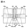
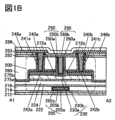
図1Aは本発明の一態様である半導体装置の上面図である。図1B乃至図1Dは本発明の一態様である半導体装置の断面図である。
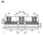
図2は本発明の一態様である半導体装置の断面図である。
図3は本発明の一態様である半導体装置の断面図である。
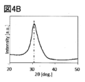
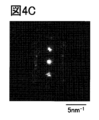
図4AはIGZOの結晶構造の分類を説明する図である。図4BはCAAC-IGZO膜のXRDスペクトルを説明する図である。図4CはCAAC-IGZO膜の極微電子線回折パターンを説明する図である。
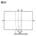
図5Aは本発明の一態様である半導体装置の作製方法を示す上面図である。図5B乃至図5Dは本発明の一態様である半導体装置の作製方法を示す断面図である。
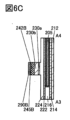
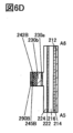
図6Aは本発明の一態様である半導体装置の作製方法を示す上面図である。図6B乃至図6Dは本発明の一態様である半導体装置の作製方法を示す断面図である。
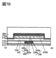
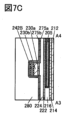
図7Aは本発明の一態様である半導体装置の作製方法を示す上面図である。図7B乃至図7Dは本発明の一態様である半導体装置の作製方法を示す断面図である。
図8Aは本発明の一態様である半導体装置の作製方法を示す上面図である。図8B乃至図8Dは本発明の一態様である半導体装置の作製方法を示す断面図である。
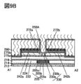
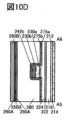
図9Aは本発明の一態様である半導体装置の作製方法を示す上面図である。図9B乃至図9Dは本発明の一態様である半導体装置の作製方法を示す断面図である。
図10Aは本発明の一態様である半導体装置の作製方法を示す上面図である。図10B乃至図10Dは本発明の一態様である半導体装置の作製方法を示す断面図である。
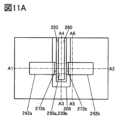
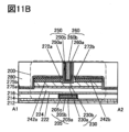
図11Aは本発明の一態様である半導体装置の作製方法を示す上面図である。図11B乃至図11Dは本発明の一態様である半導体装置の作製方法を示す断面図である。
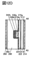
図12Aは本発明の一態様である半導体装置の作製方法を示す上面図である。図12B乃至図12Dは本発明の一態様である半導体装置の作製方法を示す断面図である。
図13Aは本発明の一態様である半導体装置の作製方法を示す上面図である。図13B乃至図13Dは本発明の一態様である半導体装置の作製方法を示す断面図である。
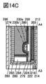
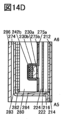
図14Aは本発明の一態様である半導体装置の上面図である。図14B乃至図14Dは本発明の一態様である半導体装置の断面図である。
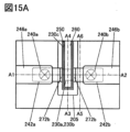
図15Aは本発明の一態様である半導体装置の上面図である。図15B乃至図15Dは本発明の一態様である半導体装置の断面図である。
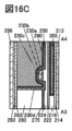
図16Aは本発明の一態様である半導体装置の上面図である。図16B乃至図16Dは本発明の一態様である半導体装置の断面図である。
図17Aおよび図17Bは本発明の一態様に係る半導体装置の断面図である。
図18は本発明の一態様に係る記憶装置の構成を示す断面図である。
図19は本発明の一態様に係る記憶装置の構成を示す断面図である。
図20Aおよび図20Bは本発明の一態様に係る半導体装置の断面図である。
図21Aおよび図21Bは本発明の一態様に係る半導体装置の断面図である。
図22は本発明の一態様に係る半導体装置の断面図である。
図23は本発明の一態様に係る半導体装置の断面図である。
図24Aは本発明の一態様に係る記憶装置の構成例を示すブロック図である。図24Bは本発明の一態様に係る記憶装置の構成例を示す模式図である。
図25A乃至図25Hは本発明の一態様に係る記憶装置の構成例を示す回路図である。
図26は各種の記憶装置を階層ごとに示す図である。
図27Aは本発明の一態様に係る半導体装置のブロック図である。図27Bは本発明の一態様に係る半導体装置の模式図である。
図28Aおよび図28Bは電子部品の一例を説明する図である。
図29A乃至図29Eは本発明の一態様に係る記憶装置の模式図である。
図30A乃至図30Hは本発明の一態様に係る電子機器を示す図である。1A is a top view of a semiconductor device according to one embodiment of the present invention, and FIGS. 1B to 1D are cross-sectional views of the semiconductor device according to one embodiment of the present invention.
FIG. 2 is a cross-sectional view of a semiconductor device according to one embodiment of the present invention.
FIG. 3 is a cross-sectional view of a semiconductor device according to one embodiment of the present invention.
Fig. 4A is a diagram for explaining the classification of IGZO crystal structures, Fig. 4B is a diagram for explaining the XRD spectrum of a CAAC-IGZO film, and Fig. 4C is a diagram for explaining the ultrafine electron beam diffraction pattern of a CAAC-IGZO film.
5A is a top view illustrating a method for manufacturing a semiconductor device according to one embodiment of the present invention, and FIGS. 5B to 5D are cross-sectional views illustrating the method for manufacturing a semiconductor device according to one embodiment of the present invention.
6A is a top view illustrating a method for manufacturing a semiconductor device according to one embodiment of the present invention, and FIGS. 6B to 6D are cross-sectional views illustrating the method for manufacturing a semiconductor device according to one embodiment of the present invention.
7A is a top view illustrating a method for manufacturing a semiconductor device according to one embodiment of the present invention, and FIGS. 7B to 7D are cross-sectional views illustrating the method for manufacturing a semiconductor device according to one embodiment of the present invention.
8A is a top view illustrating a method for manufacturing a semiconductor device according to one embodiment of the present invention, and FIGS. 8B to 8D are cross-sectional views illustrating the method for manufacturing a semiconductor device according to one embodiment of the present invention.
9A is a top view illustrating a method for manufacturing a semiconductor device according to one embodiment of the present invention, and FIGS. 9B to 9D are cross-sectional views illustrating the method for manufacturing a semiconductor device according to one embodiment of the present invention.
10A is a top view illustrating a method for manufacturing a semiconductor device according to one embodiment of the present invention, and FIGS. 10B to 10D are cross-sectional views illustrating the method for manufacturing a semiconductor device according to one embodiment of the present invention.
11A is a top view illustrating a method for manufacturing a semiconductor device according to one embodiment of the present invention, and FIGS. 11B to 11D are cross-sectional views illustrating the method for manufacturing a semiconductor device according to one embodiment of the present invention.
12A is a top view illustrating a method for manufacturing a semiconductor device according to one embodiment of the present invention, and FIGS. 12B to 12D are cross-sectional views illustrating the method for manufacturing a semiconductor device according to one embodiment of the present invention.
13A is a top view illustrating a method for manufacturing a semiconductor device according to one embodiment of the present invention, and FIGS. 13B to 13D are cross-sectional views illustrating the method for manufacturing a semiconductor device according to one embodiment of the present invention.
14A is a top view of a semiconductor device according to one embodiment of the present invention, and FIGS. 14B to 14D are cross-sectional views of the semiconductor device according to one embodiment of the present invention.
15A is a top view of a semiconductor device according to one embodiment of the present invention, and FIGS. 15B to 15D are cross-sectional views of the semiconductor device according to one embodiment of the present invention.
16A is a top view of a semiconductor device according to one embodiment of the present invention, and FIGS. 16B to 16D are cross-sectional views of the semiconductor device according to one embodiment of the present invention.
17A and 17B are cross-sectional views of a semiconductor device according to one embodiment of the present invention.
FIG. 18 is a cross-sectional view illustrating a configuration of a memory device according to one embodiment of the present invention.
FIG. 19 is a cross-sectional view illustrating a configuration of a memory device according to one embodiment of the present invention.
20A and 20B are cross-sectional views of a semiconductor device according to one embodiment of the present invention.
21A and 21B are cross-sectional views of a semiconductor device according to one embodiment of the present invention.
FIG. 22 is a cross-sectional view of a semiconductor device according to one embodiment of the present invention.
FIG. 23 is a cross-sectional view of a semiconductor device according to one embodiment of the present invention.
24A and 24B are block diagrams illustrating a configuration example of a storage device according to one embodiment of the present invention.
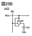
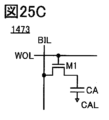
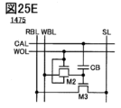
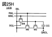
25A to 25H are circuit diagrams illustrating configuration examples of a memory device according to one embodiment of the present invention.
FIG. 26 is a diagram showing various storage devices by hierarchy.
27A and 27B are block diagrams and schematic diagrams of a semiconductor device according to one embodiment of the present invention.
28A and 28B are diagrams illustrating an example of an electronic component.
29A to 29E are schematic diagrams of a memory device according to one embodiment of the present invention.
30A to 30H are diagrams illustrating electronic devices according to one embodiment of the present invention.
以下、実施の形態について図面を参照しながら説明する。ただし、実施の形態は多くの異なる態様で実施することが可能であり、趣旨およびその範囲から逸脱することなくその形態および詳細を様々に変更し得ることは、当業者であれば容易に理解される。したがって、本発明は、以下の実施の形態の記載内容に限定して解釈されるものではない。Hereinafter, the embodiments will be described with reference to the drawings. However, it will be easily understood by those skilled in the art that the embodiments can be implemented in many different ways, and that the modes and details can be changed in various ways without departing from the spirit and scope of the present invention. Therefore, the present invention should not be interpreted as being limited to the description of the following embodiments.
また、図面において、大きさ、層の厚さ、または領域は、明瞭化のために誇張されている場合がある。よって、必ずしもそのスケールに限定されない。なお、図面は、理想的な例を模式的に示したものであり、図面に示す形状または値などに限定されない。例えば、実際の製造工程において、エッチングなどの処理により層やレジストマスクなどが意図せずに目減りすることがあるが、理解を容易とするため、図に反映しないことがある。また、図面において、同一部分または同様な機能を有する部分には同一の符号を異なる図面間で共通して用い、その繰り返しの説明は省略する場合がある。また、同様の機能を指す場合には、ハッチパターンを同じくし、特に符号を付さない場合がある。In addition, in the drawings, the size, thickness of layers, or areas may be exaggerated for clarity. Therefore, the drawings are not necessarily limited to the scale. The drawings are schematic illustrations of ideal examples, and are not limited to the shapes or values shown in the drawings. For example, in an actual manufacturing process, layers, resist masks, etc. may be unintentionally thinned by etching or other processes, but this may not be reflected in the drawings to facilitate understanding. In addition, in the drawings, the same reference numerals are used in common between different drawings for the same parts or parts having similar functions, and repeated explanations may be omitted. In addition, when referring to similar functions, the same hatch pattern may be used and no particular reference numeral may be attached.
また、特に上面図(「平面図」ともいう。)や斜視図などにおいて、発明の理解を容易とするため、一部の構成要素の記載を省略する場合がある。また、一部の隠れ線などの記載を省略する場合がある。In order to facilitate understanding of the invention, particularly in top views (also called "plan views") and perspective views, some components may be omitted from the drawings, and some hidden lines may be omitted.
また、本明細書等において、第1、第2等として付される序数詞は便宜上用いるものであり、工程順または積層順を示すものではない。そのため、例えば、「第1の」を「第2の」または「第3の」などと適宜置き換えて説明することができる。また、本明細書等に記載されている序数詞と、本発明の一態様を特定するために用いられる序数詞は一致しない場合がある。In addition, in this specification, ordinal numbers such as first, second, etc. are used for convenience and do not indicate the order of steps or stacking. Therefore, for example, "first" can be appropriately replaced with "second" or "third" for explanation. In addition, the ordinal numbers described in this specification and the like may not match the ordinal numbers used to specify one embodiment of the present invention.
また、本明細書等において、「上に」、「下に」などの配置を示す語句は、構成同士の位置関係を、図面を参照して説明するために、便宜上用いている。また、構成同士の位置関係は、各構成を描写する方向に応じて適宜変化するものである。したがって、明細書で説明した語句に限定されず、状況に応じて適切に言い換えることができる。In addition, in this specification, the terms "above" and "below" indicating the arrangement are used for convenience in order to explain the positional relationship between the components with reference to the drawings. In addition, the positional relationship between the components changes as appropriate depending on the direction in which each component is depicted. Therefore, the terms are not limited to those described in the specification, and can be rephrased appropriately depending on the situation.
例えば、本明細書等において、XとYとが接続されている、と明示的に記載されている場合は、XとYとが電気的に接続されている場合と、XとYとが機能的に接続されている場合と、XとYとが直接的に接続されている場合とが、本明細書等に開示されているものとする。したがって、所定の接続関係、例えば、図または文章に示された接続関係に限定されず、図または文章に示された接続関係以外のものも、図または文章に開示されているものとする。ここで、X、Yは、対象物(例えば、装置、素子、回路、配線、電極、端子、導電膜、層、など)であるとする。For example, in the present specification, when it is explicitly stated that X and Y are connected, the case where X and Y are electrically connected, the case where X and Y are functionally connected, and the case where X and Y are directly connected are considered to be disclosed in the present specification. Therefore, it is not limited to a specific connection relationship, for example, a connection relationship shown in a figure or text, and a connection relationship other than that shown in a figure or text is also considered to be disclosed in the figure or text. Here, X and Y are objects (for example, a device, an element, a circuit, wiring, an electrode, a terminal, a conductive film, a layer, etc.).
また、本明細書等において、トランジスタとは、ゲートと、ドレインと、ソースとを含む少なくとも三つの端子を有する素子である。そして、ドレイン(ドレイン端子、ドレイン領域またはドレイン電極)とソース(ソース端子、ソース領域またはソース電極)の間にチャネルが形成される領域(以下、チャネル形成領域ともいう。)を有しており、チャネル形成領域を介して、ソースとドレインとの間に電流を流すことができるものである。なお、本明細書等において、チャネル形成領域とは、電流が主として流れる領域をいう。In this specification, a transistor is an element having at least three terminals including a gate, a drain, and a source. A region where a channel is formed between the drain (drain terminal, drain region, or drain electrode) and the source (source terminal, source region, or source electrode) (hereinafter, also referred to as a channel formation region) is provided, and a current can flow between the source and the drain through the channel formation region. In this specification, a channel formation region refers to a region where a current mainly flows.
また、ソースやドレインの機能は、異なる極性のトランジスタを採用する場合や、回路動作において電流の方向が変化する場合などには入れ替わることがある。このため、本明細書等においては、ソースやドレインの用語は、入れ替えて用いることができる場合がある。Furthermore, the functions of the source and drain may be interchanged when transistors of different polarities are used, when the direction of current changes during circuit operation, etc. For this reason, in this specification and the like, the terms source and drain may be used interchangeably.
なお、チャネル長とは、例えば、トランジスタの上面図において、半導体(またはトランジスタがオン状態のときに半導体の中で電流の流れる部分)とゲート電極とが互いに重なる領域、またはチャネル形成領域における、ソース(ソース領域またはソース電極)とドレイン(ドレイン領域またはドレイン電極)との間の距離をいう。なお、一つのトランジスタにおいて、チャネル長が全ての領域で同じ値をとるとは限らない。すなわち、一つのトランジスタのチャネル長は、一つの値に定まらない場合がある。そのため、本明細書では、チャネル長は、チャネル形成領域における、いずれか一の値、最大値、最小値または平均値とする。The channel length refers to, for example, a region where the semiconductor (or a portion in the semiconductor through which current flows when the transistor is on) and the gate electrode overlap in a top view of the transistor, or a distance between the source (source region or source electrode) and the drain (drain region or drain electrode) in the channel formation region. Note that the channel length of one transistor does not necessarily have the same value in all regions. That is, the channel length of one transistor may not be determined to a single value. Therefore, in this specification, the channel length is defined as any one value, maximum value, minimum value, or average value in the channel formation region.
チャネル幅とは、例えば、トランジスタの上面図において、半導体(またはトランジスタがオン状態のときに半導体の中で電流の流れる部分)とゲート電極とが互いに重なる領域、またはチャネル形成領域における、チャネル長方向を基準として垂直方向のチャネル形成領域の長さをいう。なお、一つのトランジスタにおいて、チャネル幅がすべての領域で同じ値をとるとは限らない。すなわち、一つのトランジスタのチャネル幅は、一つの値に定まらない場合がある。そのため、本明細書では、チャネル幅は、チャネル形成領域における、いずれか一の値、最大値、最小値または平均値とする。The channel width refers to, for example, the length of a channel formation region in a vertical direction based on the channel length direction in a region where a semiconductor (or a portion in the semiconductor through which current flows when the transistor is on) and a gate electrode overlap each other in a top view of a transistor, or in a channel formation region. Note that the channel width of one transistor does not necessarily have the same value in all regions. In other words, the channel width of one transistor may not be determined to one value. Therefore, in this specification, the channel width is defined as any one value, maximum value, minimum value, or average value in the channel formation region.
なお、本明細書等において、トランジスタの構造によっては、実際にチャネルの形成される領域におけるチャネル幅(以下、「実効的なチャネル幅」ともいう。)と、トランジスタの上面図において示されるチャネル幅(以下、「見かけ上のチャネル幅」ともいう。)と、が異なる場合がある。例えば、ゲート電極が半導体の側面を覆う場合、実効的なチャネル幅が、見かけ上のチャネル幅よりも大きくなり、その影響が無視できなくなる場合がある。例えば、微細かつゲート電極が半導体の側面を覆うトランジスタでは、半導体の側面に形成されるチャネル形成領域の割合が大きくなる場合がある。その場合は、見かけ上のチャネル幅よりも、実効的なチャネル幅の方が大きくなる。In this specification and the like, depending on the structure of a transistor, the channel width in a region where a channel is actually formed (hereinafter also referred to as an "effective channel width") may differ from the channel width shown in a top view of the transistor (hereinafter also referred to as an "apparent channel width"). For example, when a gate electrode covers a side surface of a semiconductor, the effective channel width may be larger than the apparent channel width, and the influence of this may not be negligible. For example, in a fine transistor in which a gate electrode covers a side surface of a semiconductor, the proportion of a channel formation region formed on the side surface of the semiconductor may be large. In that case, the effective channel width is larger than the apparent channel width.
このような場合、実効的なチャネル幅の、実測による見積もりが困難となる場合がある。例えば、設計値から実効的なチャネル幅を見積もるためには、半導体の形状が既知という仮定が必要である。したがって、半導体の形状が正確にわからない場合には、実効的なチャネル幅を正確に測定することは困難である。In such a case, it may be difficult to estimate the effective channel width by actual measurement. For example, in order to estimate the effective channel width from the design value, it is necessary to assume that the shape of the semiconductor is known. Therefore, if the shape of the semiconductor is not precisely known, it is difficult to accurately measure the effective channel width.
本明細書では、単にチャネル幅と記載した場合には、見かけ上のチャネル幅を指す場合がある。または、本明細書では、単にチャネル幅と記載した場合には、実効的なチャネル幅を指す場合がある。なお、チャネル長、チャネル幅、実効的なチャネル幅、見かけ上のチャネル幅などは、断面TEM像などを解析することなどによって、値を決定することができる。In this specification, when simply referred to as a channel width, it may refer to an apparent channel width. Alternatively, when simply referred to as a channel width, it may refer to an effective channel width. Note that the values of the channel length, channel width, effective channel width, apparent channel width, etc. can be determined by analyzing a cross-sectional TEM image, etc.
なお、半導体の不純物とは、例えば、半導体を構成する主成分以外をいう。例えば、濃度が0.1原子%未満の元素は不純物と言える。不純物が含まれることにより、例えば、半導体の欠陥準位密度が高くなることや、結晶性が低下することなどが起こる場合がある。半導体が酸化物半導体である場合、半導体の特性を変化させる不純物としては、例えば、第1族元素、第2族元素、第13族元素、第14族元素、第15族元素、酸化物半導体の主成分以外の遷移金属などがあり、例えば、水素、リチウム、ナトリウム、シリコン、ホウ素、リン、炭素、窒素などがある。なお、水も不純物として機能する場合がある。また、例えば不純物の混入によって、酸化物半導体に酸素欠損(VOと表記する場合がある)が形成される場合がある。 Note that the impurity of a semiconductor refers to, for example, anything other than the main component constituting the semiconductor. For example, an element with a concentration of less than 0.1 atomic % can be said to be an impurity. When an impurity is contained, for example, the defect level density of the semiconductor may increase, or the crystallinity may decrease. When the semiconductor is an oxide semiconductor, examples of impurities that change the characteristics of the semiconductor include, for example,
なお、本明細書等において、酸化窒化シリコンとは、その組成として、窒素よりも酸素の含有量が多いものである。また、窒化酸化シリコンとは、その組成として、酸素よりも窒素の含有量が多いものである。In this specification and the like, silicon oxynitride refers to a material having a composition that contains more oxygen than nitrogen, and silicon nitride oxide refers to a material having a composition that contains more nitrogen than oxygen.
また、本明細書等において、「絶縁体」という用語を、絶縁膜または絶縁層と言い換えることができる。また、「導電体」という用語を、導電膜または導電層と言い換えることができる。また、「半導体」という用語を、半導体膜または半導体層と言い換えることができる。In this specification and the like, the term "insulator" can be replaced with an insulating film or an insulating layer, the term "conductor" can be replaced with a conductive film or a conductive layer, and the term "semiconductor" can be replaced with a semiconductor film or a semiconductor layer.
また、本明細書等において、「平行」とは、二つの直線が-10度以上10度以下の角度で配置されている状態をいう。したがって、-5度以上5度以下の場合も含まれる。また、「概略平行」とは、二つの直線が-30度以上30度以下の角度で配置されている状態をいう。また、「垂直」とは、二つの直線が80度以上100度以下の角度で配置されている状態をいう。したがって、85度以上95度以下の場合も含まれる。また、「概略垂直」とは、二つの直線が60度以上120度以下の角度で配置されている状態をいう。In addition, in this specification, "parallel" refers to a state in which two straight lines are arranged at an angle of -10 degrees or more and 10 degrees or less. Therefore, it also includes the case of -5 degrees or more and 5 degrees or less. "Approximately parallel" refers to a state in which two straight lines are arranged at an angle of -30 degrees or more and 30 degrees or less. "Perpendicular" refers to a state in which two straight lines are arranged at an angle of 80 degrees or more and 100 degrees or less. Therefore, it also includes the case of 85 degrees or more and 95 degrees or less. "Approximately perpendicular" refers to a state in which two straight lines are arranged at an angle of 60 degrees or more and 120 degrees or less.
本明細書等において、金属酸化物(metal oxide)とは、広い意味での金属の酸化物である。金属酸化物は、酸化物絶縁体、酸化物導電体(透明酸化物導電体を含む。)、酸化物半導体(Oxide Semiconductorまたは単にOSともいう。)などに分類される。例えば、トランジスタの半導体層に金属酸化物を用いた場合、当該金属酸化物を酸化物半導体と呼称する場合がある。つまり、OSトランジスタと記載する場合においては、金属酸化物または酸化物半導体を有するトランジスタと換言することができる。In this specification and the like, a metal oxide is an oxide of a metal in a broad sense. Metal oxides are classified into oxide insulators, oxide conductors (including transparent oxide conductors), oxide semiconductors (also referred to as oxide semiconductors or simply as OS), and the like. For example, when a metal oxide is used for a semiconductor layer of a transistor, the metal oxide may be referred to as an oxide semiconductor. In other words, an OS transistor can be rephrased as a transistor having a metal oxide or an oxide semiconductor.
また、本明細書等において、ノーマリーオフとは、ゲートに電位を印加しない、またはゲートに接地電位を与えたときに、トランジスタに流れるチャネル幅1μmあたりのドレイン電流が、室温において1×10-20A以下、85℃において1×10-18A以下、または125℃において1×10-16A以下であることをいう。 In addition, in this specification and the like, normally-off means that when no potential is applied to the gate or when a ground potential is applied to the gate, the drain current per 1 μm of channel width flowing in the transistor is 1×10 −20 A or less at room temperature, 1×10 −18 A or less at 85° C., or 1×10 −16 A or less at 125° C.
(実施の形態1)
本実施の形態では、図1A乃至図16Dを用いて、本発明の一態様に係るトランジスタ200を有する半導体装置の一例、およびその作製方法について説明する。(Embodiment 1)
In this embodiment, an example of a semiconductor device including a
<半導体装置の構成例>
図1A乃至図1Dを用いて、トランジスタ200を有する半導体装置の構成を説明する。図1A乃至図1Dは、トランジスタ200を有する半導体装置の上面図および断面図である。図1Aは、当該半導体装置の上面図である。また、図1B乃至図1Dは、当該半導体装置の断面図である。ここで、図1Bは、図1AにA1-A2の一点鎖線で示す部位の断面図であり、トランジスタ200のチャネル長方向の断面図でもある。また、図1Cは、図1AにA3-A4の一点鎖線で示す部位の断面図であり、トランジスタ200のチャネル幅方向の断面図でもある。また、図1Dは、図1AにA5-A6の一点鎖線で示す部位の断面図である。なお、図1Aの上面図では、図の明瞭化のために一部の要素を省いている。<Configuration Example of Semiconductor Device>
A structure of a semiconductor device including a
本発明の一態様の半導体装置は、基板(図示せず)上の絶縁体212と、絶縁体212上の絶縁体214と、絶縁体214上のトランジスタ200と、トランジスタ200上の絶縁体280と、絶縁体280上の絶縁体282と、絶縁体282上の絶縁体283と、を有する。絶縁体212、絶縁体214、絶縁体280、絶縁体282、および絶縁体283は層間膜として機能する。また、トランジスタ200と電気的に接続し、プラグとして機能する導電体240a、および導電体240bを有する。なお、導電体240aの側面に接して絶縁体241aが設けられ、導電体240bの側面に接して絶縁体241bが設けられる。また、絶縁体283上、導電体240a上、および導電体240b上には、導電体240a、および導電体240bとそれぞれ電気的に接続し、配線として機能する導電体246a、および導電体246bが設けられる。また、導電体246a上、導電体246b上、および絶縁体283上には、絶縁体286が設けられる。A semiconductor device of one embodiment of the present invention includes an
絶縁体280、絶縁体282、絶縁体283などの開口の側壁に接して絶縁体241aが設けられ、絶縁体241aの側面に接して導電体240aの第1の導電体が設けられ、さらに内側に導電体240aの第2の導電体が設けられている。また、絶縁体280、絶縁体282、絶縁体283などの開口の側壁に接して絶縁体241bが設けられ、絶縁体241bの側面に接して導電体240bの第1の導電体が設けられ、さらに内側に導電体240bの第2の導電体が設けられている。ここで、導電体240aおよび導電体240bの上面の高さと、導電体246aまたは導電体246bと重なる領域の、絶縁体283の上面の高さと、は同程度にできる。なお、トランジスタ200では、導電体240aの第1の導電体および導電体240aの第2の導電体を積層し、導電体240bの第1の導電体および導電体240bの第2の導電体を積層する構成について示しているが、本発明はこれに限られるものではない。例えば、導電体240aおよび導電体240bのそれぞれを単層、または3層以上の積層構造として設ける構成にしてもよい。構造体が積層構造を有する場合、形成順に序数を付与し、区別する場合がある。
[トランジスタ200]
図1A乃至図1Dに示すように、トランジスタ200は、絶縁体214上の絶縁体216と、絶縁体214および/または絶縁体216に埋め込まれるように配置された導電体205(導電体205a、導電体205b、および導電体205c)と、絶縁体216上、および導電体205上の絶縁体222と、絶縁体222上の絶縁体224と、絶縁体224上の酸化物230aと、酸化物230a上の酸化物230bと、酸化物230b上の導電体242a、および導電体242bと、酸化物230b上の絶縁体250(絶縁体250a、および絶縁体250b)と、絶縁体250上に位置し、酸化物230bの一部と重なる導電体260(導電体260a、および導電体260b)と、酸化物230b上、かつ、導電体242aと絶縁体250aとの間に位置する酸化物272aと、酸化物230b上、かつ、導電体242bと絶縁体250aとの間に位置する酸化物272bと、絶縁体224、酸化物230a、酸化物230b、導電体242a、導電体242b、酸化物272a、および酸化物272bの上に配置される絶縁体275(絶縁体275a、および絶縁体275b)と、を有する。ここで、図1Bおよび図1Cに示すように、導電体260の上面は、絶縁体250の上面、および絶縁体280の上面と略一致して配置される。また、絶縁体282は、導電体260、絶縁体250、および絶縁体280のそれぞれの上面と接する。[Transistor 200]
As shown in FIGS. 1A to 1D , the
なお、以下において、酸化物230aと酸化物230bをまとめて酸化物230と呼ぶ場合がある。In the following,
絶縁体280および絶縁体275には、酸化物230bに達する開口が設けられる。当該開口内に、絶縁体250、および導電体260が配置されている。また、トランジスタ200のチャネル長方向において、導電体242aと、導電体242bとの間に導電体260、絶縁体250、酸化物272a、および酸化物272bが設けられている。絶縁体250は、導電体260の側面と接する領域と、導電体260の底面と接する領域と、を有する。酸化物272aは、導電体242aの側面と接する領域と、絶縁体250aの側面と接する領域と、酸化物230bの上面と接する領域と、を有する。酸化物272bは、導電体242bの側面と接する領域と、絶縁体250aの側面と接する領域と、酸化物230bの上面と接する領域と、を有する。The
酸化物230は、絶縁体224の上に配置された酸化物230aと、酸化物230aの上に配置された酸化物230bと、を有することが好ましい。酸化物230b下に酸化物230aを有することで、酸化物230aよりも下方に形成された構造物から、酸化物230bへの不純物の拡散を抑制することができる。The
なお、トランジスタ200では、酸化物230が、酸化物230a、および酸化物230bの2層を積層する構成について示しているが、本発明はこれに限られるものではない。例えば、酸化物230bの単層、または3層以上の積層構造を設ける構成にしてもよいし、酸化物230a、および酸化物230bのそれぞれが積層構造を有していてもよい。Note that, in the
導電体260は、第1のゲート(トップゲートともいう。)電極として機能し、導電体205は、第2のゲート(バックゲートともいう。)電極として機能する。また、絶縁体222、絶縁体224、および絶縁体250は、ゲート絶縁体として機能する。また、導電体242aは、ソースまたはドレインの一方として機能し、導電体242bは、ソースまたはドレインの他方として機能する。また、酸化物230の導電体260と重畳する領域の少なくとも一部はチャネル形成領域として機能する。The
ここで、図1Bにおけるチャネル形成領域近傍の拡大図を図2に示す。図2に示すように、酸化物230bは、トランジスタ200のチャネル形成領域として機能する領域236と、ソース領域またはドレイン領域として機能する領域238aおよび領域238bと、を有する。領域236は、少なくとも一部が導電体260と重畳している。言い換えると、領域236は、導電体242aと導電体242bの間の領域に設けられている。領域238aは、導電体242aと重畳し、領域238bは、導電体242bと重畳している。Here, an enlarged view of the vicinity of the channel formation region in FIG. 1B is shown in FIG. 2. As shown in FIG. 2, the
トランジスタ200は、チャネル形成領域を含む酸化物230(酸化物230a、および酸化物230b)に、半導体として機能する金属酸化物(以下、酸化物半導体ともいう。)を用いることが好ましい。In the
また、半導体として機能する金属酸化物は、バンドギャップが2eV以上のものを用いることが好ましく、2.5eV以上のものを用いることがより好ましい。このように、バンドギャップの大きい金属酸化物を用いることで、トランジスタのオフ電流を低減することができる。The metal oxide functioning as a semiconductor preferably has a band gap of 2 eV or more, and more preferably has a band gap of 2.5 eV or more. By using a metal oxide having a wide band gap in this manner, the off-state current of a transistor can be reduced.
酸化物230として、例えば、インジウム、元素Mおよび亜鉛を有するIn-M-Zn酸化物(元素Mは、アルミニウム、ガリウム、イットリウム、錫、銅、バナジウム、ベリリウム、ホウ素、チタン、鉄、ニッケル、ゲルマニウム、ジルコニウム、モリブデン、ランタン、セリウム、ネオジム、ハフニウム、タンタル、タングステン、またはマグネシウムなどから選ばれた一種、または複数種)等の金属酸化物を用いるとよい。また、酸化物230として、In-Ga酸化物、In-Zn酸化物、インジウム酸化物などを用いてもよい。For example, a metal oxide such as In-M-Zn oxide having indium, element M, and zinc (element M is one or more selected from aluminum, gallium, yttrium, tin, copper, vanadium, beryllium, boron, titanium, iron, nickel, germanium, zirconium, molybdenum, lanthanum, cerium, neodymium, hafnium, tantalum, tungsten, magnesium, etc.) may be used as the
ここで、酸化物230bに用いる金属酸化物における、元素Mに対するInの原子数比が、酸化物230aに用いる金属酸化物における、元素Mに対するInの原子数比より大きいことが好ましい。元素Mに対するInの原子数比が小さいほど、不純物および酸素の拡散を抑制する傾向がある。よって、酸化物230bの下に酸化物230aを配置することで、酸化物230aよりも下方に形成された構造物からの、酸化物230bに対する、不純物および酸素の拡散を抑制することができる。Here, it is preferable that the atomic ratio of In to element M in the metal oxide used for
酸化物230bは、結晶性を有することが好ましい。特に、酸化物230bとして、CAAC-OS(c-axis aligned crystalline oxide semiconductor)を用いることが好ましい。The
CAAC-OSは、結晶性の高い、緻密な構造を有しており、不純物や欠陥(例えば、酸素欠損など)が少ない金属酸化物である。特に、金属酸化物の形成後に、金属酸化物が多結晶化しない程度の温度(例えば、400℃以上600℃以下)で加熱処理することで、CAAC-OSをより結晶性の高い、緻密な構造にすることができる。このようにして、CAAC-OSの密度をより高めることで、当該CAAC-OS中の不純物または酸素の拡散をより低減することができる。CAAC-OS is a metal oxide having a highly crystalline and dense structure and few impurities and defects (such as oxygen vacancies). In particular, by performing heat treatment at a temperature at which the metal oxide does not become polycrystallized (for example, 400° C. or higher and 600° C. or lower) after the formation of the metal oxide, the CAAC-OS can have a more crystalline and dense structure. By increasing the density of the CAAC-OS in this manner, the diffusion of impurities or oxygen in the CAAC-OS can be further reduced.
また、CAAC-OSは、明確な結晶粒界を確認することが難しいため、結晶粒界に起因する電子移動度の低下が起こりにくいといえる。したがって、CAAC-OSを有する金属酸化物は、物理的性質が安定する。そのため、CAAC-OSを有する金属酸化物は熱に強く、信頼性が高い。In addition, since it is difficult to identify clear crystal boundaries in CAAC-OS, it can be said that a decrease in electron mobility due to crystal boundaries is unlikely to occur. Therefore, the physical properties of metal oxides having CAAC-OS are stable. Therefore, metal oxides having CAAC-OS are resistant to heat and highly reliable.
酸化物半導体を用いたトランジスタは、酸化物半導体中のチャネル形成領域に不純物および酸素欠損が存在すると、電気特性が変動しやすく、信頼性が悪くなる場合がある。また、酸素欠損近傍の水素が、酸素欠損に水素が入った欠陥(以下、VOHと呼ぶ場合がある。)を形成し、キャリアとなる電子を生成する場合がある。このため、酸化物半導体中のチャネル形成領域に酸素欠損が含まれていると、トランジスタはノーマリーオン特性(ゲート電極に電圧を印加しなくてもチャネルが存在し、トランジスタに電流が流れる特性)となりやすい。したがって、酸化物半導体中のチャネル形成領域では、不純物、酸素欠損、およびVOHはできる限り低減されていることが好ましい。言い換えると、酸化物半導体中のチャネルが形成される領域は、キャリア濃度が低減され、i型(真性化)または実質的にi型であることが好ましい。 When impurities and oxygen vacancies are present in a channel formation region of an oxide semiconductor, the electrical characteristics of a transistor using an oxide semiconductor may fluctuate, and the reliability may be reduced. In addition, hydrogen near the oxygen vacancies may form defects (hereinafter, sometimes referred to as VOH ) in which hydrogen is inserted into the oxygen vacancies, and may generate electrons that serve as carriers. For this reason, when oxygen vacancies are present in a channel formation region of an oxide semiconductor, the transistor is likely to have normally-on characteristics (characteristics in which a channel exists and a current flows through the transistor even when no voltage is applied to the gate electrode). Therefore, impurities, oxygen vacancies, and VOH are preferably reduced as much as possible in the channel formation region of the oxide semiconductor. In other words, it is preferable that the region in the oxide semiconductor in which a channel is formed has a reduced carrier concentration and is i-type (intrinsic) or substantially i-type.
しかしながら、i型または実質的にi型である領域が、酸化物半導体中のソース領域またはドレイン領域にまで広がると、トランジスタ200のオン電流の低下、電界効果移動度の低下などを引き起こす恐れがある。However, if the i-type or substantially i-type region extends to the source or drain region in the oxide semiconductor, this may cause a decrease in the on-state current of the
よって、酸化物半導体中において、チャネル形成領域として機能する領域236は、キャリア濃度が低減され、i型または実質的にi型であることが好ましいが、ソース領域またはドレイン領域として機能する領域238aおよび領域238bは、キャリア濃度が高く、n型であることが好ましい。Therefore, in the oxide semiconductor, the
また、トランジスタを微細化することで、ソース領域とドレイン領域との間の距離が短くなり、トランジスタのソース-ドレイン耐圧が低下する恐れがある。また、領域236と領域238aまたは領域238bとの境界での電流密度が集中し、チャネルとソースまたはドレインとの境界における発熱が生じる恐れがある。Furthermore, by miniaturizing the transistor, the distance between the source region and the drain region becomes shorter, which may reduce the source-drain breakdown voltage of the transistor. Also, current density may concentrate at the boundary between the
そこで、本発明の一態様では、酸化物230bの、領域236と領域238aとの間に領域237aが設けられ、領域236と領域238bとの間に領域237bが設けられることが好ましい。Therefore, in one embodiment of the present invention, it is preferable that
さらに、領域237aのキャリア濃度は、領域238aのキャリア濃度と同等、またはそれよりも低く、領域236のキャリア濃度と同等、またはそれよりも高いことが好ましい。また、領域237bのキャリア濃度は、領域238bのキャリア濃度と同等、またはそれよりも低く、領域236のキャリア濃度と同等、またはそれよりも高いことが好ましい。つまり、領域237aは、領域236と領域238aとのオフセット領域として機能し、領域237bは、領域236と領域238bとのオフセット領域として機能する。Furthermore, it is preferable that the carrier concentration of
ここで、トランジスタのゲート長について説明する。ゲート長とは、トランジスタ動作時にキャリアがチャネル形成領域内部を移動する方向における、ゲート電極の長さであり、トランジスタの上面図における、ゲート電極の底面の幅をいう。つまり、トランジスタ200のチャネル長方向の断面視において、ゲート長は、酸化物230と重なる領域の、導電体260の底面の幅である。言い換えると、ゲート長は、領域236の幅に相当する。なお、ゲート電極の底面が緩やかな曲面を有する場合や、ゲート電極が底面に向かってテーパーがついた形状を有する場合がある。このときのゲート長は、トランジスタの上面図における、ゲート電極の底面の幅よりも大きくなる場合がある。Here, the gate length of the transistor will be described. The gate length is the length of the gate electrode in the direction in which carriers move inside the channel formation region when the transistor is operating, and refers to the width of the bottom surface of the gate electrode in the top view of the transistor. That is, in a cross-sectional view of the channel length direction of the
ここで、トランジスタの実効的なチャネル長について説明する。実効的なチャネル長とは、トランジスタの上面図において、ソース電極とドレイン電極との間の距離をいう。つまり、トランジスタ200のチャネル長方向の断面視において、実効的なチャネル長は、導電体242aと導電体242bとの間の距離である。言い換えると、実効的なチャネル長は、領域237aの幅と、領域236の幅と、領域237bの幅との和に相当する。なお、ソース電極の側面が、ソース電極の被形成面に対して傾斜し、ドレイン電極の側面が、ドレイン電極の被形成面に対して傾斜している場合、実効的なチャネル長とは、トランジスタの上面図において、ソース電極の側面の底部と、ドレイン電極の側面の底部との間の距離をいう。Here, the effective channel length of a transistor will be described. The effective channel length refers to the distance between the source electrode and the drain electrode in a top view of the transistor. That is, in a cross-sectional view of the
酸化物230bに領域237aおよび領域237bを設けることで、実効的なチャネル長を伸長することができる。よって、トランジスタのソース-ドレイン耐圧を向上させることができ、信頼性の高いトランジスタを実現できる。また、領域236と領域238aまたは領域238bとの境界での電流密度を緩和でき、チャネルとソースまたはドレインとの境界における発熱が抑制され、信頼性の高いトランジスタ、および半導体装置とすることができる。したがって、トランジスタが微細化されても、良好な電気特性を得ることができる。By providing the
トランジスタ200のチャネル長方向の断面視において、領域237aおよび領域237bの幅のそれぞれは、代表的には、1nm以上10nm未満、好ましくは3nm以上8nm未満である。なお、トランジスタ200のチャネル長方向の断面視における、領域237aの幅は、領域237aの、領域236と領域238aとの間の長さと言い換えることができる。また、トランジスタ200のチャネル長方向の断面視における、領域237bの幅は、領域237bの、領域236と領域238bとの間の長さと言い換えることができる。このとき、トランジスタ200のチャネル長方向の断面視において、チャネル形成領域として機能する領域236の幅が5nm以上40nm以下であっても、良好な電気特性を得ることができる。なお、トランジスタ200のチャネル長方向の断面視における、領域236の幅は、領域236の、領域237aと領域237bとの間の長さと言い換えることができる。In a cross-sectional view of the
チャネル形成領域として機能する領域236のキャリア濃度は、1×1017cm-3未満であることが好ましく、1×1016cm-3未満であることがより好ましく、1×1013cm-3未満であることがさらに好ましく、1×1012cm-3未満であることがさらに好ましい。なお、領域236のキャリア濃度の下限値については、特に限定は無いが、例えば、1×10⁻⁹cm-3とすることができる。 The carrier concentration of the
また、ソース領域またはドレイン領域として機能する領域238aおよび領域238bのキャリア濃度は、1×1017cm-3以上1×1021cm-3未満であることが好ましく、1×1018cm-3以上1×1020cm-3未満であることがより好ましい。 The carrier concentration of the
また、領域237a、および領域237bのキャリア濃度は、領域236、領域238a、および領域238bのキャリア濃度にもよるが、代表的には、1×1015cm-3以上1×1017cm-3以下、好ましくは5×1015cm-3以上1×1016cm-3以下である。 The carrier concentration of
なお、酸化物230bに領域237aを設けるには、導電体242aと絶縁体250aとの間に酸化物272aが配置されることが好ましい。このとき、領域237aは、酸化物272aと接する領域を有する。酸化物272aを設けることで、絶縁体280、絶縁体250aなどが有する酸素を、酸化物272aを介して、領域237aに供給することができる。よって、領域237a中の酸素欠損を低減し、領域237aのキャリア濃度を低くすることができる。また、トランジスタのチャネル長方向の断面視において、酸化物272aの幅は、1nm以上10nm未満であることが好ましく、3nm以上8nm未満であることがより好ましい。なお、トランジスタのチャネル長方向の断面視における、酸化物272aの幅は、導電体242aと絶縁体250aとの間の、酸化物272aの膜厚と言い換えることができる。In order to provide the
同様に、酸化物230bに領域237bを設けるには、導電体242bと絶縁体250aとの間に酸化物272bが配置されることが好ましい。このとき、領域237bは、酸化物272bと接する領域を有する。酸化物272bを設けることで、絶縁体280、絶縁体250aなどが有する酸素を、酸化物272bを介して、領域237bに供給することができる。よって、領域237b中の酸素欠損を低減し、領域237bのキャリア濃度を低くすることができる。また、トランジスタのチャネル長方向の断面視において、酸化物272bの幅は、1nm以上10nm未満であることが好ましく、3nm以上8nm未満であることがより好ましい。なお、トランジスタのチャネル長方向の断面視における、酸化物272bの幅は、導電体242bと絶縁体250aとの間の、酸化物272bの膜厚と言い換えることができる。Similarly, to provide the
トランジスタ200のチャネル長方向の断面視における、酸化物272aおよび酸化物272bの幅を上記にすることで、ゲート長または領域236の幅が5nm以上40nm以下であっても、良好な電気特性を得ることができる。By setting the widths of
酸化物272a、および酸化物272bは、それぞれ導電体242a、および導電体242bの側端部が酸化されることで、形成される場合がある。よって、酸化物272a、および酸化物272bは、それぞれ導電体242a、および導電体242bが有する金属を含む場合がある。例えば、導電体242a、および導電体242bとして、タンタルを含む窒化物を用いる場合、酸化物272a、および酸化物272bのそれぞれは、タンタルと、酸素と、を有する。The
また、酸化物272a、および酸化物272bは、絶縁体250aとも接する。よって、酸化物272a、および酸化物272bは、導電体242a、および導電体242bが有する金属に加えて、絶縁体250aが有する元素を含む場合がある。例えば、絶縁体250aとして、酸化シリコン、または酸化窒化シリコンなどを用いる場合、酸化物272a、および酸化物272bのそれぞれは、タンタルと、シリコンと、酸素と、を有する場合がある。The
酸化物272aおよび酸化物272bは、それぞれ、導電体242aおよび導電体242bよりも酸素を多く含むため、絶縁性を有すると推定される。よって、酸化物272aおよび酸化物272bを、semi-insulator(SI)と呼ぶことができる場合がある。領域237aおよび領域237bのキャリア濃度は、領域238aおよび領域238bのキャリア濃度と同等、またはそれよりも低く、領域236のキャリア濃度と同等、またはそれよりも高いため、領域237aおよび領域237bをSIまたはSI領域と呼ぶことができる場合がある。領域236を、I型または実質的にI型であるとみなし、領域238aおよび領域238bを、N型またはN+型であるとみなすと、トランジスタ200は、(N+-SI-I-SI-N+)構造を有するといえる。The
また、酸化物230b上に導電体242aおよび導電体242bを設けた状態で、酸素を含む雰囲気でマイクロ波処理を行うことが好ましい。ここで、マイクロ波処理とは、例えばマイクロ波を用いて高密度プラズマを発生させる電源を有する装置を用いた処理のことを指す。In addition, it is preferable to perform microwave treatment in an atmosphere containing oxygen with the
酸素を含む雰囲気でマイクロ波処理を行うことで、マイクロ波、またはRF等の高周波を用いて酸素ガスをプラズマ化し、当該酸素プラズマを作用させることができる。このとき、マイクロ波、またはRF等の高周波を領域236、領域237a、および領域237bに照射することもできる。プラズマ、マイクロ波などの作用により、領域236、領域237a、および領域237bのVOHを分断し、水素を領域236、領域237a、および領域237bから除去し、酸素欠損を酸素で補填することができる。つまり、領域236、領域237a、および領域237bにおいて、「VOH→H+VO」という反応が起きて、領域236、領域237a、および領域237bの水素濃度を低減することができる。よって、領域236中、領域237a中、および領域237b中の酸素欠損、およびVOHを低減し、キャリア濃度を低下させることができる。 By performing microwave processing in an atmosphere containing oxygen, oxygen gas can be turned into plasma using microwaves or high frequency waves such as RF, and the oxygen plasma can be made to act. At this time, microwaves or high frequency waves such as RF can also be irradiated to the
また、酸素を含む雰囲気でマイクロ波処理を行う際、マイクロ波、またはRF等の高周波、酸素プラズマなどの作用は、導電体242aおよび導電体242bに遮蔽され、領域238aおよび領域238bには及ばない。さらに、酸素プラズマの作用は、酸化物230b、導電体242a、および導電体242bを覆って設けられている、絶縁体275および絶縁体280によって低減することができる。これにより、マイクロ波処理の際に、領域238aおよび領域238bで、VOHの低減、および過剰な量の酸素供給が発生しないので、キャリア濃度の低下を防ぐことができる。 Furthermore, when microwave processing is performed in an atmosphere containing oxygen, the effects of microwaves, high frequency waves such as RF, oxygen plasma, etc. are shielded by
また、酸素を含む雰囲気でマイクロ波処理を行う際、マイクロ波、またはRF等の高周波、酸素プラズマなどの作用は、酸化物272a、酸化物272b、絶縁体275、および絶縁体280によって低減することができる。よって、領域237a、および領域237bへの当該作用は、領域236よりも弱く、領域238aおよび領域238bよりも強い。したがって、マイクロ波処理による、領域237aおよび領域237bのキャリア濃度は、領域238aおよび領域238bよりも低下し、領域236ほど低下しない。Furthermore, when microwave processing is performed in an atmosphere containing oxygen, the effects of microwaves, high frequency waves such as RF, oxygen plasma, and the like can be reduced by
このようにして、酸化物半導体の領域236で選択的に酸素欠損、およびVOHを除去して、領域236をi型または実質的にi型とすることができる。さらに、ソース領域またはドレイン領域として機能する領域238aおよび領域238bに過剰な酸素が供給されるのを抑制し、n型を維持することができる。さらに、領域237aおよび領域237bのキャリア濃度は、領域238aおよび領域238bのキャリア濃度と同等、またはそれよりも低く、領域236のキャリア濃度と同等、またはそれよりも高くすることができる。これにより、トランジスタ200の電気特性の変動が抑制され、基板面内でトランジスタ200の電気特性がばらつくのを抑制することができる。 In this manner, oxygen vacancies and VOH can be selectively removed from the
このように、開示する発明の一態様では、微細化に伴う問題点を解消することができるため、結果として、トランジスタサイズを十分に小さくすることが可能になる。トランジスタサイズを十分に小さくすることで、トランジスタを用いた半導体装置の占める面積が小さくなるため、基板あたりの半導体装置の取り数が増大する。これにより、半導体装置あたりの製造コストは抑制される。また、半導体装置が小型化されるため、同程度の大きさでさらに機能が高められた半導体装置を実現することができる。つまり、開示する発明の一態様により酸化物半導体を用いたトランジスタの微細化が達成されることで、これに付随する様々な効果を得ることが可能である。In this manner, one embodiment of the disclosed invention can solve problems associated with miniaturization, and as a result, the size of a transistor can be sufficiently reduced. By sufficiently reducing the size of a transistor, the area occupied by a semiconductor device using the transistor is reduced, and the number of semiconductor devices that can be manufactured per substrate is increased. This reduces the manufacturing cost per semiconductor device. In addition, since the semiconductor device is miniaturized, a semiconductor device with improved functions can be realized with a similar size. In other words, by miniaturizing a transistor using an oxide semiconductor according to one embodiment of the disclosed invention, various associated effects can be obtained.
なお、図2では、領域236、領域237a、領域237b、領域238a、および領域238bが酸化物230bに形成される例について示しているが、本発明はこれに限られるものではない。例えば、上記の各領域が酸化物230bだけでなく、酸化物230aまで形成されてもよい。2 shows an example in which the
また、図2では、領域236の幅が絶縁体250aの幅と一致しているが、本実施の形態は、これに限られるものではない。領域236の幅が絶縁体250aの幅より狭くなる場合、または領域236の幅が絶縁体250aの幅より広くなる場合もある。例えば、図3に示すように、領域236の幅が導電体260の底面の幅と一致する場合がある。2, the width of the
また、図2では、領域237aの幅は、酸化物272aの幅と一致している。なお、本実施の形態は、これに限られるものではない。例えば、領域237aの幅は、酸化物272aの幅より狭くなる場合、または酸化物272aの幅より広くなる場合もある。また、領域237aが、導電体242aと重なる領域を有する場合、導電体260と重なる領域を有する場合もある。例えば、図3に示すように、領域237aの幅は、導電体260に対向する導電体242aの側面と導電体260との間の距離と一致する場合がある。なお、領域237bの幅についても、領域237aの幅と同様のことがいえる。2, the width of the
また、酸化物230において、各領域の境界を明確に検出することが困難な場合がある。各領域内で検出される金属元素、ならびに水素、および窒素などの不純物元素の濃度は、領域ごとの段階的な変化に限らず、各領域内でも連続的に変化していてもよい。つまり、チャネル形成領域に近い領域であるほど、金属元素、ならびに水素、および窒素などの不純物元素の濃度が減少していればよい。In addition, it may be difficult to clearly detect the boundaries between the regions in the
以上のような構成にすることで、トランジスタ特性のばらつきが少ない半導体装置を提供することができる。また、信頼性が良好な半導体装置を提供することができる。また、良好な電気特性を有する半導体装置を提供することができる。また、微細化または高集積化が可能な半導体装置を提供することができる。By adopting the above-mentioned configuration, it is possible to provide a semiconductor device with less variation in transistor characteristics. It is also possible to provide a semiconductor device with good reliability. It is also possible to provide a semiconductor device with good electrical characteristics. It is also possible to provide a semiconductor device that can be miniaturized or highly integrated.
なお、図1Bなどにおいて、導電体260等を埋め込む開口の側面が、酸化物230bの溝部も含めて、酸化物230bの被形成面に対して概略垂直となっているが、本実施の形態はこれに限られるものではない。例えば、図3に示すように、当該開口の底部が緩やかな曲面を有する、U字型の形状となってもよい。また、例えば、当該開口の側面が酸化物230bの被形成面に対して傾斜していてもよい。In Fig. 1B and other figures, the side of the opening in which the
また、図1Cに示すように、トランジスタ200のチャネル幅方向の断面視において、酸化物230bの側面と酸化物230bの上面との間に、湾曲面を有してもよい。つまり、当該側面の端部と当該上面の端部は、湾曲してもよい(以下、ラウンド状ともいう。)。1C , in a cross-sectional view of the
上記湾曲面での曲率半径は、0nmより大きく、導電体242aまたは導電体242bと重なる領域の酸化物230bの膜厚より小さい、または、上記湾曲面を有さない領域の長さの半分より小さいことが好ましい。上記湾曲面での曲率半径は、具体的には、0nmより大きく20nm以下、好ましくは1nm以上15nm以下、さらに好ましくは2nm以上10nm以下とする。このような形状にすることで、絶縁体250および導電体260の、酸化物230bへの被覆性を高めることができる。The radius of curvature of the curved surface is preferably greater than 0 nm and smaller than the film thickness of the
酸化物230は、化学組成が異なる複数の酸化物層の積層構造を有することが好ましい。具体的には、酸化物230aに用いる金属酸化物において、主成分である金属元素に対する元素Mの原子数比が、酸化物230bに用いる金属酸化物における、主成分である金属元素に対する元素Mの原子数比より、大きいことが好ましい。また、酸化物230aに用いる金属酸化物において、Inに対する元素Mの原子数比が、酸化物230bに用いる金属酸化物における、Inに対する元素Mの原子数比より大きいことが好ましい。また、酸化物230bに用いる金属酸化物において、元素Mに対するInの原子数比が、酸化物230aに用いる金属酸化物における、元素Mに対するInの原子数比より大きいことが好ましい。The
また、酸化物230bは、CAAC-OSなどの結晶性を有する酸化物であることが好ましい。CAAC-OSなどの結晶性を有する酸化物は、不純物や欠陥(酸素欠損など)が少なく、結晶性の高い、緻密な構造を有している。よって、ソース電極またはドレイン電極による、酸化物230bからの酸素の引き抜きを抑制することができる。これにより、熱処理を行っても、酸化物230bから酸素が引き抜かれることを低減できるので、トランジスタ200は、製造工程における高い温度(所謂サーマルバジェット)に対して安定である。In addition, the
ここで、酸化物230aと酸化物230bの接合部において、伝導帯下端はなだらかに変化する。換言すると、酸化物230aと酸化物230bの接合部における伝導帯下端は、連続的に変化または連続接合するともいうことができる。このようにするためには、酸化物230aと酸化物230bとの界面に形成される混合層の欠陥準位密度を低くするとよい。Here, the conduction band minimum changes gradually at the junction between the
具体的には、酸化物230aと酸化物230bが、酸素以外に共通の元素を主成分として有することで、欠陥準位密度が低い混合層を形成することができる。例えば、酸化物230bがIn-M-Zn酸化物の場合、酸化物230aとして、In-M-Zn酸化物、M-Zn酸化物、元素Mの酸化物、In-Zn酸化物、インジウム酸化物などを用いてもよい。Specifically, when the
具体的には、酸化物230aとして、In:M:Zn=1:3:4[原子数比]もしくはその近傍の組成、またはIn:M:Zn=1:1:0.5[原子数比]もしくはその近傍の組成の金属酸化物を用いればよい。また、酸化物230bとして、In:M:Zn=1:1:1[原子数比]もしくはその近傍の組成、またはIn:M:Zn=4:2:3[原子数比]もしくはその近傍の組成の金属酸化物を用いればよい。なお、近傍の組成とは、所望の原子数比の±30%の範囲を含む。また、元素Mとして、ガリウムを用いることが好ましい。Specifically, the
なお、金属酸化物をスパッタリング法により成膜する場合、上記の原子数比は、成膜された金属酸化物の原子数比に限られず、金属酸化物の成膜に用いるスパッタリングターゲットの原子数比であってもよい。In addition, when a metal oxide film is formed by a sputtering method, the above atomic ratio is not limited to the atomic ratio of the formed metal oxide film, but may be the atomic ratio of a sputtering target used to form the metal oxide film.
酸化物230aおよび酸化物230bを上述の構成とすることで、酸化物230aと酸化物230bとの界面における欠陥準位密度を低くすることができる。そのため、界面散乱によるキャリア伝導への影響が小さくなり、トランジスタ200は大きいオン電流、および高い周波数特性を得ることができる。By configuring the
トランジスタ200において、絶縁体224上の酸化物230は、少なくとも一部がチャネル形成領域として機能する。なお、SOI(Silicon On Insulator)構造において、絶縁膜上のシリコン膜は、少なくとも一部がチャネル形成領域として機能する。よって、SOI構造は、広義にとらえると、Semiconductor On Insulator構造とみなすことができる。よって、トランジスタ200は、SOI構造を有するといえる。In the
また、絶縁体224上の酸化物230は、島状に形成されている。よって、同一基板上に、複数のトランジスタ200を設けることができる。よって、本発明の一態様により、集積化構造を形成することができる。The
絶縁体212、絶縁体214、絶縁体275、絶縁体282、絶縁体283、および絶縁体286の少なくとも一は、水、水素などの不純物が、基板側から、または、トランジスタ200の上方からトランジスタ200に拡散するのを抑制するバリア絶縁膜として機能することが好ましい。したがって、絶縁体212、絶縁体214、絶縁体275、絶縁体282、絶縁体283、および絶縁体286の少なくとも一は、水素原子、水素分子、水分子、窒素原子、窒素分子、酸化窒素分子(N2O、NO、NO2など)、銅原子などの不純物の拡散を抑制する機能を有する(上記不純物が透過しにくい)絶縁性材料を用いることが好ましい。または、酸素(例えば、酸素原子、酸素分子などの少なくとも一)の拡散を抑制する機能を有する(上記酸素が透過しにくい)絶縁性材料を用いることが好ましい。 At least one of the
なお、本明細書において、バリア絶縁膜とは、バリア性を有する絶縁膜のことを指す。本明細書において、バリア性とは、対応する物質の拡散を抑制する機能(透過性が低いともいう)とする。または、対応する物質を、捕獲、および固着する(ゲッタリングともいう)機能とする。In this specification, a barrier insulating film refers to an insulating film having a barrier property. In this specification, the barrier property refers to a function of suppressing the diffusion of a corresponding substance (also referred to as low permeability) or a function of capturing and fixing a corresponding substance (also referred to as gettering).
絶縁体212、絶縁体214、絶縁体275、絶縁体282、絶縁体283、および絶縁体286としては、水、水素などの不純物、および酸素の拡散を抑制する機能を有する絶縁体を用いることが好ましく、例えば、酸化アルミニウム、酸化マグネシウム、酸化ハフニウム、酸化ガリウム、インジウムガリウム亜鉛酸化物、窒化シリコン、または窒化酸化シリコンなどを用いることができる。例えば、絶縁体212、絶縁体283、および絶縁体286として、より水素バリア性が高い、窒化シリコンなどを用いることが好ましい。また、例えば、絶縁体214、絶縁体275、および絶縁体282として、水素を捕獲および水素を固着する機能が高い、酸化アルミニウムまたは酸化マグネシウムなどを用いることが好ましい。これにより、水、水素などの不純物が絶縁体212、および絶縁体214を介して、基板側からトランジスタ200側に拡散するのを抑制することができる。または、水、水素などの不純物が絶縁体286よりも外側に配置されている層間絶縁膜などから、トランジスタ200側に拡散するのを抑制することができる。または、絶縁体224などに含まれる酸素が、絶縁体212、および絶縁体214を介して基板側に拡散するのを抑制することができる。または、絶縁体280などに含まれる酸素が、絶縁体282などを介してトランジスタ200より上方に拡散するのを抑制することができる。この様に、トランジスタ200を、水、水素などの不純物、および酸素の拡散を抑制する機能を有する絶縁体212、絶縁体214、絶縁体275、絶縁体282、絶縁体283、および絶縁体286で取り囲む構造とすることが好ましい。For the
ここで、絶縁体212、絶縁体214、絶縁体275、絶縁体282、絶縁体283、および絶縁体286として、アモルファス構造を有する酸化物を用いることが好ましい。例えば、AlOx(xは0より大きい任意数)、またはMgOy(yは0より大きい任意数)などの金属酸化物を用いることが好ましい。このようなアモルファス構造を有する金属酸化物では、酸素原子がダングリングボンドを有しており、当該ダングリングボンドで水素を捕獲または固着する性質を有する場合がある。このようなアモルファス構造を有する金属酸化物をトランジスタ200の構成要素として用いる、またはトランジスタ200の周囲に設けることで、トランジスタ200に含まれる水素、またはトランジスタ200の周囲に存在する水素を捕獲または固着することができる。特にトランジスタ200のチャネル形成領域に含まれる水素を捕獲または固着することが好ましい。アモルファス構造を有する金属酸化物をトランジスタ200の構成要素として用いる、またはトランジスタ200の周囲に設けることで、良好な特性を有し、信頼性の高いトランジスタ200、および半導体装置を作製することができる。 Here, it is preferable to use an oxide having an amorphous structure as the
また、絶縁体212、絶縁体214、絶縁体275、絶縁体282、絶縁体283、および絶縁体286は、アモルファス構造であることが好ましいが、一部に多結晶構造の領域が形成されていてもよい。また、絶縁体212、絶縁体214、絶縁体275、絶縁体282、絶縁体283、および絶縁体286は、アモルファス構造の層と、多結晶構造の層と、が積層された多層構造であってもよい。例えば、アモルファス構造の層の上に多結晶構造の層が形成された積層構造でもよい。Furthermore, the
絶縁体212、絶縁体214、絶縁体275、絶縁体282、絶縁体283、および絶縁体286の成膜は、例えば、スパッタリング法を用いて行えばよい。スパッタリング法は、成膜ガスに水素を用いなくてよいので、絶縁体212、絶縁体214、絶縁体275、絶縁体282、絶縁体283、および絶縁体286の水素濃度を低減することができる。なお、成膜方法は、スパッタリング法に限られるものではなく、化学気相成長(CVD:Chemical Vapor Deposition)法、分子線エピタキシー(MBE:Molecular Beam Epitaxy)法、パルスレーザ堆積(PLD:Pulsed Laser Deposition)法、原子層堆積(ALD:Atomic Layer Deposition)法などを適宜用いてもよい。The
また、絶縁体212、絶縁体283、および絶縁体286の抵抗率を低くすることが好ましい場合がある。例えば、絶縁体212、絶縁体283、および絶縁体286の抵抗率を概略1×10¹³Ωcmとすることで、半導体装置作製工程のプラズマ等を用いる処理において、絶縁体212、絶縁体283、および絶縁体286が、導電体205、導電体242a、導電体242b、導電体260、導電体246a、または導電体246bのチャージアップを緩和することができる場合がある。絶縁体212、絶縁体283、および絶縁体286の抵抗率は、好ましくは、1×10¹⁰Ωcm以上1×10¹⁵Ωcm以下とする。 It may be preferable to reduce the resistivity of the
また、絶縁体216、および絶縁体280は、絶縁体214よりも誘電率が低いことが好ましい。誘電率が低い材料を層間膜とすることで、配線間に生じる寄生容量を低減することができる。例えば、絶縁体216、および絶縁体280として、酸化シリコン、酸化窒化シリコン、窒化酸化シリコン、窒化シリコン、フッ素を添加した酸化シリコン、炭素を添加した酸化シリコン、炭素および窒素を添加した酸化シリコン、空孔を有する酸化シリコンなどを適宜用いればよい。特に、酸化シリコンおよび酸化窒化シリコンは、熱的に安定であるため好ましい。特に、酸化シリコン、酸化窒化シリコン、空孔を有する酸化シリコンなどの材料は、加熱により脱離する酸素を含む領域を容易に形成することができるため好ましい。Moreover, the
導電体205は、酸化物230、および導電体260と、重なるように配置する。ここで、導電体205は、絶縁体214および/または絶縁体216に形成された開口に埋め込まれて設けることが好ましい。The
導電体205は、導電体205a、導電体205b、および導電体205cを有する。導電体205aは、当該開口の底面および側壁に接して設けられる。導電体205bは、導電体205aに形成された凹部に埋め込まれるように設けられる。ここで、導電体205bの上面は、導電体205aの上面および絶縁体216の上面より低くなる。導電体205cは、導電体205bの上面、および導電体205aの側面に接して設けられる。ここで、導電体205cの上面の高さは、導電体205aの上面の高さおよび絶縁体216の上面の高さと略一致する。つまり、導電体205bは、導電体205aおよび導電体205cに包み込まれる構成になる。The
ここで、導電体205aおよび導電体205cは、水素原子、水素分子、水分子、窒素原子、窒素分子、酸化窒素分子(N2O、NO、NO2など)、銅原子などの不純物の拡散を抑制する機能を有する導電性材料を用いることが好ましい。または、酸素(例えば、酸素原子、酸素分子などの少なくとも一)の拡散を抑制する機能を有する導電性材料を用いることが好ましい。 Here, the
導電体205aおよび導電体205cに、水素の拡散を低減する機能を有する導電性材料を用いることにより、導電体205bに含まれる水素などの不純物が、絶縁体224等を介して、酸化物230に拡散するのを防ぐことができる。また、導電体205aおよび導電体205cに、酸素の拡散を抑制する機能を有する導電性材料を用いることにより、導電体205bが酸化して導電率が低下することを抑制することができる。酸素の拡散を抑制する機能を有する導電性材料としては、例えば、チタン、窒化チタン、タンタル、窒化タンタル、ルテニウム、酸化ルテニウムなどを用いることが好ましい。したがって、導電体205aおよび導電体205cとしては、上記導電性材料を単層または積層とすればよい。例えば、導電体205aおよび導電体205cは、窒化チタンを用いればよい。By using a conductive material having a function of reducing hydrogen diffusion for the
また、導電体205bは、タングステン、銅、またはアルミニウムを主成分とする導電性材料を用いることが好ましい。例えば、導電体205bは、タングステンを用いればよい。The
導電体205は、第2のゲート電極として機能する場合がある。その場合、導電体205に印加する電位を、導電体260に印加する電位と、連動させず、独立して変化させることで、トランジスタ200のしきい値電圧(Vth)を制御することができる。特に、導電体205に負の電位を印加することにより、トランジスタ200のVthをより大きくし、オフ電流を低減することが可能となる。したがって、導電体205に負の電位を印加したほうが、印加しない場合よりも、導電体260に印加する電位が0Vのときのドレイン電流を小さくすることができる。The
また、導電体205の電気抵抗率は、上記の導電体205に印加する電位を考慮して設計され、導電体205の膜厚は当該電気抵抗率に合わせて設定される。また、絶縁体216の膜厚は、導電体205とほぼ同じになる。ここで、導電体205の設計が許す範囲で導電体205および絶縁体216の膜厚を薄くすることが好ましい。絶縁体216の膜厚を薄くすることで、絶縁体216中に含まれる水素などの不純物の絶対量を低減することができるので、当該不純物が酸化物230に拡散するのを低減することができる。The electrical resistivity of the
なお、導電体205は、図1Aに示すように、酸化物230の導電体242aおよび導電体242bと重ならない領域の大きさよりも、大きく設けるとよい。特に、図1Cに示すように、導電体205は、酸化物230aおよび酸化物230bのチャネル幅方向と交わる端部よりも外側の領域においても、延伸していることが好ましい。つまり、酸化物230のチャネル幅方向における側面の外側において、導電体205と、導電体260とは、絶縁体を介して重畳していることが好ましい。当該構成を有することで、第1のゲート電極として機能する導電体260の電界と、第2のゲート電極として機能する導電体205の電界によって、酸化物230のチャネル形成領域を電気的に取り囲むことができる。本明細書において、第1のゲート、および第2のゲートの電界によって、チャネル形成領域を電気的に取り囲むトランジスタの構造を、surrounded channel(S-channel)構造とよぶ。As shown in FIG. 1A, the
なお、本明細書等において、S-channel構造のトランジスタとは、一対のゲート電極の一方および他方の電界によって、チャネル形成領域を電気的に取り囲むトランジスタの構造を表す。また、本明細書等で開示するS-channel構造は、Fin型構造およびプレーナ型構造とは異なる。S-channel構造を採用することで、短チャネル効果に対する耐性を高める、別言すると短チャネル効果が発生し難いトランジスタとすることができる。In this specification and the like, a transistor with an S-channel structure refers to a transistor structure in which a channel formation region is electrically surrounded by the electric fields of one and the other of a pair of gate electrodes. The S-channel structure disclosed in this specification and the like is different from a fin type structure and a planar type structure. By employing the S-channel structure, it is possible to provide a transistor that is more resistant to the short channel effect, in other words, in which the short channel effect is less likely to occur.
また、図1Cに示すように、導電体205は延伸させて、配線としても機能させている。ただし、これに限られることなく、導電体205の下に、配線として機能する導電体を設ける構成にしてもよい。また、導電体205は、必ずしも各トランジスタに一個ずつ設ける必要はない。例えば、導電体205を複数のトランジスタで共有する構成にしてもよい。1C, the
なお、トランジスタ200では、導電体205は、導電体205a、導電体205b、および導電体205cを積層する構成について示しているが、本発明はこれに限られるものではない。例えば、導電体205は、単層、2層または4層以上の積層構造として設ける構成にしてもよい。Note that, in the
絶縁体222、および絶縁体224は、ゲート絶縁体として機能する。The
絶縁体222は、水素(例えば、水素原子、水素分子などの少なくとも一)の拡散を抑制する機能を有することが好ましい。また、絶縁体222は、酸素(例えば、酸素原子、酸素分子などの少なくとも一)の拡散を抑制する機能を有することが好ましい。例えば、絶縁体222は、絶縁体224よりも水素および酸素の一方または双方の拡散を抑制する機能を有することが好ましい。The
絶縁体222は、絶縁性材料であるアルミニウムおよびハフニウムの一方または双方の酸化物を含む絶縁体を用いるとよい。当該絶縁体として、酸化アルミニウム、酸化ハフニウム、アルミニウムおよびハフニウムを含む酸化物(ハフニウムアルミネート)などを用いることが好ましい。このような材料を用いて絶縁体222を形成した場合、絶縁体222は、酸化物230から基板側への酸素の放出や、トランジスタ200の周辺部から酸化物230への水素等の不純物の拡散を抑制する層として機能する。よって、絶縁体222を設けることで、水素等の不純物が、トランジスタ200の内側へ拡散することを抑制し、酸化物230中の酸素欠損の生成を抑制することができる。また、導電体205が、絶縁体224や、酸化物230が有する酸素と反応することを抑制することができる。The
または、上記絶縁体に、例えば、酸化アルミニウム、酸化ビスマス、酸化ゲルマニウム、酸化ニオブ、酸化シリコン、酸化チタン、酸化タングステン、酸化イットリウム、酸化ジルコニウムを添加してもよい。または、これらの絶縁体を窒化処理してもよい。また、絶縁体222は、これらの絶縁体に酸化シリコン、酸化窒化シリコンまたは窒化シリコンを積層して用いてもよい。Alternatively, for example, aluminum oxide, bismuth oxide, germanium oxide, niobium oxide, silicon oxide, titanium oxide, tungsten oxide, yttrium oxide, or zirconium oxide may be added to the insulator. Alternatively, these insulators may be nitrided. Furthermore, the
また、絶縁体222は、例えば、酸化アルミニウム、酸化ハフニウム、酸化タンタル、酸化ジルコニウム、チタン酸ジルコン酸鉛(PZT)、チタン酸ストロンチウム(SrTiO3)、(Ba,Sr)TiO3(BST)などのいわゆるhigh-k材料を含む絶縁体を単層または積層で用いてもよい。トランジスタの微細化、および高集積化が進むと、ゲート絶縁体の薄膜化により、リーク電流などの問題が生じる場合がある。ゲート絶縁体として機能する絶縁体にhigh-k材料を用いることで、物理膜厚を保ちながら、トランジスタ動作時のゲート電位の低減が可能となる。 The
酸化物230と接する絶縁体224は、過剰酸素を含む(加熱により酸素を脱離する)ことが好ましい。例えば、絶縁体224は、酸化シリコン、酸化窒化シリコンなどを適宜用いればよい。酸素を含む絶縁体を酸化物230に接して設けることにより、酸化物230中の酸素欠損を低減し、トランジスタ200の信頼性を向上させることができる。The
絶縁体224として、具体的には、加熱により一部の酸素が脱離する酸化物材料、別言すると、過剰酸素領域を有する絶縁体材料を用いることが好ましい。加熱により酸素を脱離する酸化膜とは、TDS(Thermal Desorption Spectroscopy)分析にて、酸素分子の脱離量が1.0×10¹⁸molecules/cm3以上、好ましくは1.0×1019molecules/cm3以上、さらに好ましくは2.0×1019molecules/cm3以上、または3.0×1020molecules/cm3以上である酸化膜である。なお、上記TDS分析時における膜の表面温度としては100℃以上700℃以下、または100℃以上400℃以下の範囲が好ましい。 Specifically, it is preferable to use an oxide material from which part of oxygen is released by heating, in other words, an insulator material having an excess oxygen region, as the
また、トランジスタ200の作製工程中において、酸化物230の表面が露出した状態で、加熱処理を行うと好適である。当該加熱処理は、例えば、100℃以上600℃以下、より好ましくは350℃以上550℃以下で行えばよい。なお、加熱処理は、窒素ガスもしくは不活性ガスの雰囲気、または酸化性ガスを10ppm以上、1%以上、もしくは10%以上含む雰囲気で行う。例えば、加熱処理は酸素雰囲気で行うことが好ましい。これにより、酸化物230に酸素を供給して、酸素欠損の低減を図ることができる。また、加熱処理は減圧状態で行ってもよい。または、加熱処理は、窒素ガスもしくは不活性ガスの雰囲気で加熱処理した後に、脱離した酸素を補うために、酸化性ガスを10ppm以上、1%以上、または10%以上含む雰囲気で行ってもよい。または、酸化性ガスを10ppm以上、1%以上、または10%以上含む雰囲気で加熱処理した後に、連続して窒素ガスもしくは不活性ガスの雰囲気で加熱処理を行っても良い。In addition, in a manufacturing process of the
なお、酸化物230に加酸素化処理を行うことで、酸化物230中の酸素欠損を、供給された酸素により修復させる、別言すると「VO+O→null」という反応を促進させることができる。さらに、酸化物230中に残存した水素に供給された酸素が反応することで、当該水素をH2Oとして除去する(脱水化する)ことができる。これにより、酸化物230中に残存していた水素が酸素欠損に再結合してVOHが形成されるのを抑制することができる。 By performing oxygen addition treatment on the
なお、絶縁体222、および絶縁体224が、2層以上の積層構造を有していてもよい。その場合、同じ材料からなる積層構造に限定されず、異なる材料からなる積層構造でもよい。また、絶縁体224は、酸化物230aと重畳して島状に形成してもよい。この場合、絶縁体275が、絶縁体224の側面および絶縁体222の上面に接する構成になる。The
導電体242a、および導電体242bは酸化物230bの上面に接して設けられることが好ましい。導電体242aおよび導電体242bは、それぞれトランジスタ200のソース電極またはドレイン電極として機能する。The
導電体242aおよび導電体242bとしては、例えば、タンタルを含む窒化物、チタンを含む窒化物、モリブデンを含む窒化物、タングステンを含む窒化物、タンタルおよびアルミニウムを含む窒化物、チタンおよびアルミニウムを含む窒化物などを用いることが好ましい。本発明の一態様においては、タンタルを含む窒化物が特に好ましい。また、例えば、酸化ルテニウム、窒化ルテニウム、ストロンチウムとルテニウムを含む酸化物、ランタンとニッケルを含む酸化物などを用いてもよい。これらの材料は、酸化しにくい導電性材料、または、酸素を吸収しても導電性を維持する材料であるため、好ましい。As the
なお、酸化物230bなどに含まれる水素が、導電体242aまたは導電体242bに拡散する場合がある。特に、導電体242aおよび導電体242bに、タンタルを含む窒化物を用いることで、酸化物230bなどに含まれる水素は、導電体242aまたは導電体242bに拡散しやすく、拡散した水素は、導電体242aまたは導電体242bが有する窒素と結合することがある。つまり、酸化物230bなどに含まれる水素は、導電体242aまたは導電体242bに吸い取られる場合がある。Note that hydrogen contained in the
また、導電体242aの側面と導電体242aの上面との間、および導電体242bの側面と導電体242bの上面との間に、湾曲面が形成されないことが好ましい。当該湾曲面が形成されない導電体242aおよび導電体242bとすることで、図1Dに示すような、チャネル幅方向の断面における、導電体242aおよび導電体242bの断面積を大きくすることができる。これにより、導電体242aおよび導電体242bの導電率を大きくし、トランジスタ200のオン電流を大きくすることができる。It is also preferable that no curved surface is formed between the side surface of the
絶縁体275は、絶縁体224、酸化物230a、酸化物230b、導電体242a、および導電体242bを覆って設けられており、絶縁体250、および導電体260が設けられる領域に開口が形成されている。絶縁体275は、絶縁体224の上面、酸化物230aの側面、酸化物230bの側面、導電体242aの側面および上面、ならびに導電体242bの側面および上面に接して絶縁体275aが設けられ、絶縁体275a上に絶縁体275bが設けられることが好ましい。The
なお、トランジスタ200では、絶縁体275が、絶縁体275a、および絶縁体275bの2層を積層する構成について示しているが、本発明はこれに限られるものではない。例えば、単層、または3層以上の積層構造を設ける構成にしてもよいし、絶縁体275a、および絶縁体275bのそれぞれが積層構造を有していてもよい。Note that, in the
絶縁体275は、酸素の透過を抑制するバリア絶縁膜として機能することが好ましい。また、絶縁体275は、水、水素などの不純物が、上方から絶縁体224に拡散するのを抑制するバリア絶縁膜として機能することが好ましく、水素などの不純物を捕獲する機能を有することが好ましい。その場合、絶縁体275としては、アモルファス構造を有する金属酸化物、例えば、酸化アルミニウムまたは酸化マグネシウムなどの絶縁体を含むことが好ましい。絶縁体275としては、例えば、酸化アルミニウム、および窒化シリコンなどの絶縁体を単層で、または積層して用いればよい。絶縁体275として、酸化アルミニウム、および窒化シリコンを積層して用いる場合、絶縁体275aとして酸化アルミニウムを設け、絶縁体275bとして窒化シリコンを設けることが好ましい。The
また、絶縁体275の少なくとも一部に酸化アルミニウムを用いる場合、該酸化アルミニウムは、アモルファス構造を有する酸化アルミニウム、またはアモルファス構造の酸化アルミニウムであることが好ましい。アモルファス構造を有する金属酸化物、特に、アモルファス構造を有する酸化アルミニウム、およびアモルファス構造の酸化アルミニウムは、周囲に存在する水素を捕獲または固着することができる場合があるため、良好な特性を有し、信頼性の高いトランジスタ200、および半導体装置を作製することができる。Furthermore, when aluminum oxide is used for at least a part of the
絶縁体212と絶縁体283に挟まれた領域内で、絶縁体280、または絶縁体224に接して、水素などの不純物を捕獲する機能を有する、絶縁体275を設けることで、絶縁体280、または絶縁体224に含まれる水素などの不純物を捕獲し、当該領域内における、水素の量を一定値にすることができる。この場合は、絶縁体275として、酸化アルミニウムなどを用いることが好ましい。By providing an
絶縁体250(絶縁体250a、および絶縁体250b)は、ゲート絶縁体として機能する。酸化物230bの上面に接して絶縁体250aが配置され、絶縁体250a上に絶縁体250bが配置される。絶縁体250は、例えば、酸化シリコン、酸化窒化シリコン、窒化酸化シリコン、窒化シリコン、フッ素を添加した酸化シリコン、炭素を添加した酸化シリコン、炭素および窒素を添加した酸化シリコン、空孔を有する酸化シリコンなどを用いることができる。特に、酸化シリコン、および酸化窒化シリコンは熱に対し安定であるため好ましい。The insulator 250 (
絶縁体250は、絶縁体224と同様に、絶縁体250中の水、水素などの不純物濃度が低減されていることが好ましい。絶縁体250の膜厚は、1nm以上20nm以下とするのが好ましい。The
絶縁体250aは、加熱により酸素が放出される絶縁体を用いて形成し、絶縁体250bは、酸素の拡散を抑制する機能を有する絶縁体を用いて形成することが好ましい。このような構成にすることで、絶縁体250aに含まれる酸素が、導電体260へ拡散するのを抑制することができる。つまり、酸化物230へ供給する酸素量の減少を抑制することができる。また、絶縁体250aに含まれる酸素による導電体260の酸化を抑制することができる。例えば、絶縁体250aは、上述した絶縁体250に用いることができる材料を用いて設け、絶縁体250bは、絶縁体222と同様の材料を用いて設けることができる。It is preferable that the
なお、絶縁体250aに酸化シリコンや酸化窒化シリコンなどを用いる場合、絶縁体250bは、比誘電率が高いhigh-k材料である絶縁性材料を用いてもよい。ゲート絶縁体を、絶縁体250aと絶縁体250bとの積層構造とすることで、熱に対して安定、かつ比誘電率の高い積層構造とすることができる。したがって、ゲート絶縁体の物理膜厚を保持したまま、トランジスタ動作時に印加するゲート電位の低電位化が可能となる。また、ゲート絶縁体として機能する絶縁体の等価酸化膜厚(EOT)の薄膜化が可能となる。When silicon oxide or silicon oxynitride is used for the
絶縁体250bとして、具体的には、ハフニウム、アルミニウム、ガリウム、イットリウム、ジルコニウム、タングステン、チタン、タンタル、ニッケル、ゲルマニウム、マグネシウムなどから選ばれた一種、もしくは二種以上が含まれた金属酸化物、または酸化物230として用いることができる金属酸化物を用いることができる。特に、アルミニウムおよびハフニウムの一方または双方の酸化物を含む絶縁体を用いることが好ましい。例えば、絶縁体250として、酸化シリコンと、該酸化シリコン上の酸化ハフニウムを含む積層構造を用いればよい。Specifically, the
絶縁体250を2層の積層構造にすることで、絶縁体250の物理的な厚みにより、導電体260と、酸化物230との間の距離を保つことで、導電体260と酸化物230との間のリーク電流を抑制することができる。また、導電体260と酸化物230との間の物理的な距離、および導電体260から酸化物230へかかる電界強度を、容易に適宜調整することができる。By forming the
なお、図1Bおよび図1Cでは、絶縁体250を2層の積層構造で図示したが、単層、または3層以上の積層構造としてもよい。Although the
また、絶縁体250と導電体260との間に金属酸化物を設けてもよい。当該金属酸化物は、絶縁体250から導電体260への酸素の拡散を抑制することが好ましい。酸素の拡散を抑制する金属酸化物を設けることで、絶縁体250から導電体260への酸素の拡散が抑制される。つまり、酸化物230へ供給する酸素量の減少を抑制することができる。また、絶縁体250の酸素による導電体260の酸化を抑制することができる。A metal oxide may also be provided between the
なお、上記金属酸化物は、第1のゲート電極の一部としての機能を有する構成にしてもよい。例えば、酸化物230として用いることができる金属酸化物を、上記金属酸化物として用いることができる。その場合、導電体260aをスパッタリング法で成膜することで、上記金属酸化物の電気抵抗値を低下させて導電体とすることができる。これをOC(Oxide Conductor)電極と呼ぶことができる。上記金属酸化物を有することで、導電体260からの電界の影響を弱めることなく、トランジスタ200のオン電流の向上を図ることができる。The metal oxide may have a function as a part of the first gate electrode. For example, a metal oxide that can be used as the
導電体260は、トランジスタ200の第1のゲート電極として機能する。導電体260は、導電体260aと、導電体260aの上に配置された導電体260bと、を有することが好ましい。例えば、導電体260aは、導電体260bの底面および側面を包むように配置されることが好ましい。また、図1Bおよび図1Cに示すように、導電体260の上面は、絶縁体250の上面と略一致している。なお、図1Bおよび図1Cでは、導電体260は、導電体260aと導電体260bの2層構造として示しているが、単層構造でもよいし、3層以上の積層構造であってもよい。The
導電体260aは、水素原子、水素分子、水分子、窒素原子、窒素分子、酸化窒素分子、銅原子などの不純物の拡散を抑制する機能を有する導電性材料を用いることが好ましい。または、酸素(例えば、酸素原子、酸素分子などの少なくとも一)の拡散を抑制する機能を有する導電性材料を用いることが好ましい。The
また、導電体260aが酸素の拡散を抑制する機能を持つことにより、絶縁体250に含まれる酸素により、導電体260bが酸化して導電率が低下することを抑制することができる。酸素の拡散を抑制する機能を有する導電性材料としては、例えば、チタン、窒化チタン、タンタル、窒化タンタル、ルテニウム、酸化ルテニウムなどを用いることが好ましい。Furthermore, since the
また、導電体260は、配線としても機能するため、導電性が高い導電体を用いることが好ましい。例えば、導電体260bは、タングステン、銅、またはアルミニウムを主成分とする導電性材料を用いることができる。また、導電体260bは積層構造としてもよく、例えば、チタンまたは窒化チタンと上記導電性材料との積層構造としてもよい。In addition, since the
また、トランジスタ200では、導電体260は、絶縁体280などに形成されている開口を埋めるように自己整合的に形成される。導電体260をこのように形成することにより、導電体242aと導電体242bとの間の領域に、導電体260を位置合わせすることなく確実に配置することができる。Furthermore, in the
また、図1Cに示すように、トランジスタ200のチャネル幅方向において、導電体260の、導電体260と酸化物230bとが重ならない領域の底面は、酸化物230bの底面より低いことが好ましい。ゲート電極として機能する導電体260が、絶縁体250などを介して、酸化物230bのチャネル形成領域の側面および上面を覆う構成とすることで、導電体260の電界を酸化物230bのチャネル形成領域全体に作用させやすくなる。よって、トランジスタ200のオン電流を増大させ、周波数特性を向上させることができる。絶縁体222の底面を基準としたとき、酸化物230aおよび酸化物230bと、導電体260とが、重ならない領域における導電体260の底面の高さと、酸化物230bの底面の高さと、の差は、0nm以上100nm以下、好ましくは3nm以上50nm以下、より好ましくは5nm以上20nm以下とする。1C, in the channel width direction of the
絶縁体280は、絶縁体275上に設けられ、絶縁体250、および導電体260が設けられる領域に開口が形成されている。また、絶縁体280の上面は、平坦化されていてもよい。The
絶縁体280は、絶縁体224と同様に、過剰酸素領域または過剰酸素を有することが好ましい。また、絶縁体280中の水、水素などの不純物濃度は低減されていることが好ましい。例えば、絶縁体280は、酸化シリコン、酸化窒化シリコンなどのシリコンを含む酸化物を適宜用いればよい。過剰酸素を有する絶縁体を酸化物230に接して設けることにより、酸化物230中の酸素欠損を低減し、トランジスタ200の信頼性を向上させることができる。また、絶縁体280は、上記の材料が積層された構造でもよく、例えば、スパッタリング法で成膜した酸化シリコンと、その上に積層されたCVD法で成膜された酸化窒化シリコンの積層構造とすればよい。また、さらに上に窒化シリコンを積層してもよい。Like the
絶縁体282は、水、水素などの不純物が、上方から絶縁体280に拡散するのを抑制するバリア絶縁膜として機能することが好ましく、水素などの不純物を捕獲する機能を有することが好ましい。また、絶縁体282は、酸素の透過を抑制するバリア絶縁膜として機能することが好ましい。絶縁体282としては、アモルファス構造を有する金属酸化物、例えば、酸化アルミニウムなどの絶縁体を用いればよい。絶縁体212と絶縁体283に挟まれた領域内で、絶縁体280に接して、水素などの不純物を捕獲する機能を有する、絶縁体282を設けることで、絶縁体280などに含まれる水素などの不純物を捕獲し、当該領域内における、水素の量を一定値にすることができる。特に、絶縁体282として、アモルファス構造を有する酸化アルミニウム、またはアモルファス構造の酸化アルミニウムを用いることで、より効果的に水素を捕獲または固着できる場合があるため好ましい。これにより、良好な特性を有し、信頼性の高いトランジスタ200、および半導体装置を作製することができる。The
絶縁体283は、水、水素などの不純物が、上方から絶縁体280に拡散するのを抑制するバリア絶縁膜として機能する。絶縁体283は、絶縁体282の上に配置される。絶縁体283としては、窒化シリコンまたは窒化酸化シリコンなどの、シリコンを含む窒化物を用いることが好ましい。例えば、絶縁体283としてスパッタリング法で成膜された窒化シリコンを用いればよい。絶縁体283をスパッタリング法で成膜することで、密度が高く、鬆などが形成されにくい窒化シリコン膜を形成することができる。また、絶縁体283として、スパッタリング法で成膜された窒化シリコンの上に、さらに、CVD法で成膜された窒化シリコンを積層してもよい。The
導電体240aおよび導電体240bは、タングステン、銅、またはアルミニウムを主成分とする導電性材料を用いることが好ましい。また、導電体240aおよび導電体240bは積層構造としてもよい。The
また、導電体240aおよび導電体240bのそれぞれを積層構造とする場合、絶縁体283、絶縁体282、絶縁体280、および絶縁体275と接する導電体には、水、水素などの不純物の透過を抑制する機能を有する導電性材料を用いることが好ましい。例えば、タンタル、窒化タンタル、チタン、窒化チタン、ルテニウム、酸化ルテニウムなどを用いることが好ましい。また、水、水素などの不純物の透過を抑制する機能を有する導電性材料は、単層または積層で用いてもよい。また、絶縁体283より上層に含まれる水、水素などの不純物が、導電体240aおよび導電体240bを通じて酸化物230に混入するのを抑制することができる。Furthermore, when the
絶縁体241aおよび絶縁体241bとしては、例えば、窒化シリコン、酸化アルミニウム、窒化酸化シリコンなどの絶縁体を用いればよい。絶縁体241aおよび絶縁体241bは、絶縁体283、絶縁体282、および絶縁体275に接して設けられるので、絶縁体280などに含まれる水、水素などの不純物が、導電体240aおよび導電体240bを通じて酸化物230に混入するのを抑制することができる。特に、窒化シリコンは水素に対するブロッキング性が高いので好適である。また、絶縁体280に含まれる酸素が導電体240aおよび導電体240bに吸収されるのを防ぐことができる。As the
また、導電体240aの上面、および導電体240bの上面に接して、配線として機能する導電体246a、および導電体246bを配置してもよい。導電体246a、および導電体246bは、タングステン、銅、またはアルミニウムを主成分とする導電性材料を用いることが好ましい。また、当該導電体は、積層構造としてもよく、例えば、チタンまたは窒化チタンと上記導電性材料との積層としてもよい。なお、当該導電体は、絶縁体に設けられた開口に埋め込むように形成してもよい。
絶縁体286は、導電体246a上、導電体246b上、および絶縁体283上に設けられる。これにより、導電体246aの上面、導電体246aの側面、導電体246bの上面、および導電体246bの側面は、絶縁体286と接し、導電体246aの下面、および導電体246bの下面は、絶縁体283と接する。つまり、導電体246aおよび導電体246bは、絶縁体283、および絶縁体286で包まれる構成とすることができる。この様な構成とすることで、外方からの酸素の透過を抑制し、導電体246aおよび導電体246bの酸化を防止することができる。また、導電体246aおよび導電体246bから、水、水素などの不純物が外部に拡散することを防ぐことができるので好ましい。The
<半導体装置の構成材料>
以下では、半導体装置に用いることができる構成材料について説明する。<Materials Constituting Semiconductor Device>
The following describes constituent materials that can be used in the semiconductor device.
<<基板>>
トランジスタ200を形成する基板としては、例えば、絶縁体基板、半導体基板、または導電体基板を用いればよい。絶縁体基板としては、例えば、ガラス基板、石英基板、サファイア基板、安定化ジルコニア基板(イットリア安定化ジルコニア基板など)、樹脂基板などがある。また、半導体基板としては、例えば、シリコン、ゲルマニウムを材料とした半導体基板、または炭化シリコン、シリコンゲルマニウム、ヒ化ガリウム、リン化インジウム、酸化亜鉛、酸化ガリウムからなる化合物半導体基板などがある。さらには、前述の半導体基板内部に絶縁体領域を有する半導体基板、例えば、SOI(Silicon On Insulator)基板などがある。導電体基板としては、黒鉛基板、金属基板、合金基板、導電性樹脂基板などがある。または、金属の窒化物を有する基板、金属の酸化物を有する基板などがある。さらには、絶縁体基板に導電体または半導体が設けられた基板、半導体基板に導電体または絶縁体が設けられた基板、導電体基板に半導体または絶縁体が設けられた基板などがある。または、これらの基板に素子が設けられたものを用いてもよい。基板に設けられる素子としては、容量素子、抵抗素子、スイッチ素子、発光素子、記憶素子などがある。<<Substrate>>
The substrate on which the
<<絶縁体>>
絶縁体としては、絶縁性を有する酸化物、窒化物、酸化窒化物、窒化酸化物、金属酸化物、金属酸化窒化物、金属窒化酸化物などがある。<<Insulators>>
Examples of the insulator include oxides, nitrides, oxynitrides, nitride oxides, metal oxides, metal oxynitrides, and metal nitride oxides, each of which has insulating properties.
例えば、トランジスタの微細化、および高集積化が進むと、ゲート絶縁体の薄膜化により、リーク電流などの問題が生じる場合がある。ゲート絶縁体として機能する絶縁体に、high-k材料を用いることで物理膜厚を保ちながら、トランジスタ動作時の低電圧化が可能となる。一方、層間膜として機能する絶縁体には、比誘電率が低い材料を用いることで、配線間に生じる寄生容量を低減することができる。したがって、絶縁体の機能に応じて、材料を選択するとよい。For example, as transistors become smaller and more highly integrated, problems such as leakage current may occur due to thinner gate insulators. By using a high-k material for the insulator that functions as the gate insulator, it is possible to reduce the voltage required for transistor operation while maintaining the physical film thickness. On the other hand, by using a material with a low dielectric constant for the insulator that functions as the interlayer film, it is possible to reduce the parasitic capacitance that occurs between wiring. Therefore, it is advisable to select a material according to the function of the insulator.
また、比誘電率の高い絶縁体としては、酸化ガリウム、酸化ハフニウム、酸化ジルコニウム、アルミニウムおよびハフニウムを有する酸化物、アルミニウムおよびハフニウムを有する酸化窒化物、シリコンおよびハフニウムを有する酸化物、シリコンおよびハフニウムを有する酸化窒化物、またはシリコンおよびハフニウムを有する窒化物などがある。Further, examples of insulators with a high relative dielectric constant include gallium oxide, hafnium oxide, zirconium oxide, oxides having aluminum and hafnium, oxynitrides having aluminum and hafnium, oxides having silicon and hafnium, oxynitrides having silicon and hafnium, and nitrides having silicon and hafnium.
また、比誘電率が低い絶縁体としては、酸化シリコン、酸化窒化シリコン、窒化酸化シリコン、窒化シリコン、フッ素を添加した酸化シリコン、炭素を添加した酸化シリコン、炭素および窒素を添加した酸化シリコン、空孔を有する酸化シリコン、または樹脂などがある。Examples of insulators with a low dielectric constant include silicon oxide, silicon oxynitride, silicon nitride oxide, silicon nitride, silicon oxide with fluorine added, silicon oxide with carbon added, silicon oxide with carbon and nitrogen added, silicon oxide with voids, or resin.
また、金属酸化物を用いたトランジスタは、水素などの不純物および酸素の透過を抑制する機能を有する絶縁体で囲うことによって、トランジスタの電気特性を安定にすることができる。水素などの不純物および酸素の透過を抑制する機能を有する絶縁体としては、例えば、ホウ素、炭素、窒素、酸素、フッ素、マグネシウム、アルミニウム、シリコン、リン、塩素、アルゴン、ガリウム、ゲルマニウム、イットリウム、ジルコニウム、ランタン、ネオジム、ハフニウム、またはタンタルを含む絶縁体を、単層で、または積層で用いればよい。具体的には、水素などの不純物および酸素の透過を抑制する機能を有する絶縁体として、酸化アルミニウム、酸化マグネシウム、酸化ガリウム、酸化ゲルマニウム、酸化イットリウム、酸化ジルコニウム、酸化ランタン、酸化ネオジム、酸化ハフニウム、酸化タンタルなどの金属酸化物、窒化アルミニウム、窒化酸化シリコン、窒化シリコンなどの金属窒化物を用いることができる。In addition, the transistor using metal oxide can have stable electrical characteristics by being surrounded by an insulator having a function of suppressing the permeation of impurities such as hydrogen and oxygen. As the insulator having a function of suppressing the permeation of impurities such as hydrogen and oxygen, for example, an insulator containing boron, carbon, nitrogen, oxygen, fluorine, magnesium, aluminum, silicon, phosphorus, chlorine, argon, gallium, germanium, yttrium, zirconium, lanthanum, neodymium, hafnium, or tantalum may be used in a single layer or a stacked layer. Specifically, as the insulator having a function of suppressing the permeation of impurities such as hydrogen and oxygen, metal oxides such as aluminum oxide, magnesium oxide, gallium oxide, germanium oxide, yttrium oxide, zirconium oxide, lanthanum oxide, neodymium oxide, hafnium oxide, and tantalum oxide, and metal nitrides such as aluminum nitride, silicon nitride oxide, and silicon nitride can be used.
また、ゲート絶縁体として機能する絶縁体は、加熱により脱離する酸素を含む領域を有する絶縁体であることが好ましい。例えば、加熱により脱離する酸素を含む領域を有する酸化シリコンまたは酸化窒化シリコンを酸化物230と接する構造とすることで、酸化物230が有する酸素欠損を補償することができる。The insulator that functions as the gate insulator is preferably an insulator having a region containing oxygen that is released by heating. For example, by using a structure in which silicon oxide or silicon oxynitride having a region containing oxygen that is released by heating is in contact with the
<<導電体>>
導電体としては、アルミニウム、クロム、銅、銀、金、白金、タンタル、ニッケル、チタン、モリブデン、タングステン、ハフニウム、バナジウム、ニオブ、マンガン、マグネシウム、ジルコニウム、ベリリウム、インジウム、ルテニウム、イリジウム、ストロンチウム、ランタンなどから選ばれた金属元素、または上述した金属元素を成分とする合金か、上述した金属元素を組み合わせた合金等を用いることが好ましい。例えば、窒化タンタル、窒化チタン、タングステン、チタンとアルミニウムを含む窒化物、タンタルとアルミニウムを含む窒化物、酸化ルテニウム、窒化ルテニウム、ストロンチウムとルテニウムを含む酸化物、ランタンとニッケルを含む酸化物などを用いることが好ましい。また、窒化タンタル、窒化チタン、チタンとアルミニウムを含む窒化物、タンタルとアルミニウムを含む窒化物、酸化ルテニウム、窒化ルテニウム、ストロンチウムとルテニウムを含む酸化物、ランタンとニッケルを含む酸化物は、酸化しにくい導電性材料、または、酸素を吸収しても導電性を維持する材料であるため、好ましい。また、リン等の不純物元素を含有させた多結晶シリコンに代表される、電気伝導度が高い半導体、ニッケルシリサイドなどのシリサイドを用いてもよい。<<Conductors>>
As the conductor, it is preferable to use a metal element selected from aluminum, chromium, copper, silver, gold, platinum, tantalum, nickel, titanium, molybdenum, tungsten, hafnium, vanadium, niobium, manganese, magnesium, zirconium, beryllium, indium, ruthenium, iridium, strontium, lanthanum, etc., or an alloy containing the above-mentioned metal elements as a component, or an alloy combining the above-mentioned metal elements. For example, it is preferable to use tantalum nitride, titanium nitride, tungsten, nitride containing titanium and aluminum, nitride containing tantalum and aluminum, ruthenium oxide, ruthenium nitride, oxide containing strontium and ruthenium, oxide containing lanthanum and nickel, etc. In addition, tantalum nitride, titanium nitride, nitride containing titanium and aluminum, nitride containing tantalum and aluminum, ruthenium oxide, ruthenium nitride, oxide containing strontium and ruthenium, oxide containing lanthanum and nickel are conductive materials that are difficult to oxidize, or materials that maintain conductivity even when oxygen is absorbed, so they are preferable. Furthermore, a semiconductor having high electrical conductivity, typified by polycrystalline silicon containing an impurity element such as phosphorus, or a silicide such as nickel silicide may be used.
また、上記の材料で形成される導電層を複数積層して用いてもよい。例えば、前述した金属元素を含む材料と、酸素を含む導電性材料と、を組み合わせた積層構造としてもよい。また、前述した金属元素を含む材料と、窒素を含む導電性材料と、を組み合わせた積層構造としてもよい。また、前述した金属元素を含む材料と、酸素を含む導電性材料と、窒素を含む導電性材料と、を組み合わせた積層構造としてもよい。A plurality of conductive layers formed of the above-mentioned materials may be stacked. For example, a stacked structure may be formed by combining the above-mentioned material containing a metal element and a conductive material containing oxygen. A stacked structure may be formed by combining the above-mentioned material containing a metal element and a conductive material containing nitrogen. A stacked structure may be formed by combining the above-mentioned material containing a metal element, a conductive material containing oxygen, and a conductive material containing nitrogen.
なお、トランジスタのチャネル形成領域に酸化物を用いる場合において、ゲート電極として機能する導電体には、前述した金属元素を含む材料と、酸素を含む導電性材料と、を組み合わせた積層構造を用いることが好ましい。この場合は、酸素を含む導電性材料をチャネル形成領域側に設けるとよい。酸素を含む導電性材料をチャネル形成領域側に設けることで、当該導電性材料から離脱した酸素がチャネル形成領域に供給されやすくなる。In addition, when an oxide is used for the channel formation region of a transistor, a conductor functioning as a gate electrode preferably has a stacked structure in which a material containing a metal element and a conductive material containing oxygen are combined. In this case, the conductive material containing oxygen is preferably provided on the channel formation region side. By providing the conductive material containing oxygen on the channel formation region side, oxygen released from the conductive material is easily supplied to the channel formation region.
特に、ゲート電極として機能する導電体として、チャネルが形成される金属酸化物に含まれる金属元素および酸素を含む導電性材料を用いることが好ましい。また、前述した金属元素および窒素を含む導電性材料を用いてもよい。例えば、窒化チタン、窒化タンタルなどの窒素を含む導電性材料を用いてもよい。また、インジウム錫酸化物、酸化タングステンを含むインジウム酸化物、酸化タングステンを含むインジウム亜鉛酸化物、酸化チタンを含むインジウム酸化物、酸化チタンを含むインジウム錫酸化物、インジウム亜鉛酸化物、シリコンを添加したインジウム錫酸化物を用いてもよい。また、窒素を含むインジウムガリウム亜鉛酸化物を用いてもよい。このような材料を用いることで、チャネルが形成される金属酸化物に含まれる水素を捕獲することができる場合がある。または、外方の絶縁体などから混入する水素を捕獲することができる場合がある。In particular, it is preferable to use a conductive material containing oxygen and a metal element contained in the metal oxide in which the channel is formed as a conductor functioning as a gate electrode. The conductive material containing the metal element and nitrogen described above may also be used. For example, a conductive material containing nitrogen, such as titanium nitride or tantalum nitride, may also be used. Indium tin oxide, indium oxide containing tungsten oxide, indium zinc oxide containing tungsten oxide, indium oxide containing titanium oxide, indium tin oxide containing titanium oxide, indium zinc oxide, or indium tin oxide to which silicon is added may also be used. Indium gallium zinc oxide containing nitrogen may also be used. By using such a material, hydrogen contained in the metal oxide in which the channel is formed may be captured. Alternatively, hydrogen mixed in from an external insulator may be captured.
<<金属酸化物>>
酸化物230として、半導体として機能する金属酸化物(酸化物半導体)を用いることが好ましい。以下では、本発明に係る酸化物230に適用可能な金属酸化物について説明する。<<Metal oxides>>
It is preferable to use a metal oxide that functions as a semiconductor (oxide semiconductor) as the
金属酸化物は、少なくともインジウムまたは亜鉛を含むことが好ましい。特に、インジウムおよび亜鉛を含むことが好ましい。また、それらに加えて、アルミニウム、ガリウム、イットリウム、錫などが含まれていることが好ましい。また、ホウ素、チタン、鉄、ニッケル、ゲルマニウム、ジルコニウム、モリブデン、ランタン、セリウム、ネオジム、ハフニウム、タンタル、タングステン、マグネシウム、コバルトなどから選ばれた一種、または複数種が含まれていてもよい。The metal oxide preferably contains at least indium or zinc. In particular, it is preferable that the metal oxide contains indium and zinc. In addition to these, it is preferable that the metal oxide contains aluminum, gallium, yttrium, tin, etc. In addition, it may contain one or more elements selected from boron, titanium, iron, nickel, germanium, zirconium, molybdenum, lanthanum, cerium, neodymium, hafnium, tantalum, tungsten, magnesium, cobalt, etc.
ここでは、金属酸化物が、インジウム、元素Mおよび亜鉛を有するIn-M-Zn酸化物である場合を考える。なお、元素Mは、アルミニウム、ガリウム、イットリウム、または錫とする。そのほかの元素Mに適用可能な元素としては、ホウ素、チタン、鉄、ニッケル、ゲルマニウム、ジルコニウム、モリブデン、ランタン、セリウム、ネオジム、ハフニウム、タンタル、タングステン、マグネシウム、コバルトなどがある。ただし、元素Mとして、前述の元素を複数組み合わせても構わない場合がある。Here, the case where the metal oxide is an In-M-Zn oxide having indium, an element M, and zinc is considered. The element M is aluminum, gallium, yttrium, or tin. Other elements that can be used for the element M include boron, titanium, iron, nickel, germanium, zirconium, molybdenum, lanthanum, cerium, neodymium, hafnium, tantalum, tungsten, magnesium, and cobalt. However, there are cases where a combination of a plurality of the above elements may be used as the element M.
なお、本明細書等において、窒素を有する金属酸化物も金属酸化物(metal oxide)と総称する場合がある。また、窒素を有する金属酸化物を、金属酸窒化物(metal oxynitride)と呼称してもよい。In this specification and the like, metal oxides containing nitrogen may also be collectively referred to as metal oxides. Furthermore, metal oxides containing nitrogen may also be referred to as metal oxynitrides.
<結晶構造の分類>
まず、酸化物半導体における、結晶構造の分類について、図4Aを用いて説明を行う。図4Aは、酸化物半導体、代表的にはIGZO(Inと、Gaと、Znと、を含む金属酸化物)の結晶構造の分類を説明する図である。<Classification of crystal structures>
First, classification of crystal structures in oxide semiconductors will be described with reference to Fig. 4A. Fig. 4A is a diagram for explaining classification of crystal structures of oxide semiconductors, typically IGZO (metal oxide containing In, Ga, and Zn).
図4Aに示すように、酸化物半導体は、大きく分けて「Amorphous(無定形)」と、「Crystalline(結晶性)」と、「Crystal(結晶)」と、に分類される。また、「Amorphous」の中には、completely amorphousが含まれる。また、「Crystalline」の中には、CAAC(c-axis-aligned crystalline)、nc(nanocrystalline)、及びCAC(cloud-aligned composite)が含まれる(excluding single crystal and poly crystal)。なお、「Crystalline」の分類には、single crystal、poly crystal、及びcompletely amorphousは除かれる。また、「Crystal」の中には、single crystal、及びpoly crystalが含まれる。As shown in FIG. 4A, oxide semiconductors are roughly classified into "amorphous", "crystalline", and "crystalline". In addition, "amorphous" includes completely amorphous. In addition, "crystalline" includes c-axis-aligned crystalline line (CAAC), nanocrystalline line (nc), and cloud-aligned composite (CAC) (excluding single crystal and poly crystal). In addition, the classification of "Crystalline" excludes single crystal, poly crystal, and completely amorphous. In addition, "Crystal" includes single crystal and poly crystal.
なお、図4Aに示す太枠内の構造は、「Amorphous(無定形)」と、「Crystal(結晶)」との間の中間状態であり、新しい境界領域(New crystalline phase)に属する構造である。すなわち、当該構造は、エネルギー的に不安定な「Amorphous(無定形)」や、「Crystal(結晶)」とは全く異なる構造と言い換えることができる。The structure within the bold frame shown in Fig. 4A is an intermediate state between "Amorphous" and "Crystal" and belongs to a new boundary region (New crystalline phase). In other words, this structure can be said to be a structure that is completely different from the energetically unstable "Amorphous" and "Crystal".
なお、膜または基板の結晶構造は、X線回折(XRD:X-Ray Diffraction)スペクトルを用いて評価することができる。ここで、「Crystalline」に分類されるCAAC-IGZO膜のGIXD(Grazing-Incidence XRD)測定で得られるXRDスペクトルを図4Bに示す。なお、GIXD法は、薄膜法またはSeemann-Bohlin法ともいう。以降、図4Bに示すGIXD測定で得られるXRDスペクトルを、単にXRDスペクトルと記す。なお、図4Bに示すCAAC-IGZO膜の組成は、In:Ga:Zn=4:2:3[原子数比]近傍である。また、図4Bに示すCAAC-IGZO膜の厚さは、500nmである。The crystal structure of the film or substrate can be evaluated using an X-ray diffraction (XRD) spectrum. Here, FIG. 4B shows an XRD spectrum obtained by GIXD (Grazing-Incidence XRD) measurement of the CAAC-IGZO film classified as "Crystalline". The GIXD method is also called the thin film method or the Seemann-Bohlin method. Hereinafter, the XRD spectrum obtained by the GIXD measurement shown in FIG. 4B will be simply referred to as the XRD spectrum. The composition of the CAAC-IGZO film shown in FIG. 4B is in the vicinity of In:Ga:Zn=4:2:3 [atomic ratio]. The thickness of the CAAC-IGZO film shown in FIG. 4B is 500 nm.
図4Bでは、横軸は2θ[deg.]であり、縦軸は強度(Intensity)[a.u.]である。図4Bに示すように、CAAC-IGZO膜のXRDスペクトルでは、明確な結晶性を示すピークが検出される。具体的には、CAAC-IGZO膜のXRDスペクトルでは、2θ=31°近傍に、c軸配向を示すピークが検出される。なお、図4Bに示すように、2θ=31°近傍のピークは、ピーク強度が検出された角度を軸に左右非対称である。In FIG. 4B, the horizontal axis is 2θ [deg.], and the vertical axis is intensity [a.u.]. As shown in FIG. 4B, a peak indicating clear crystallinity is detected in the XRD spectrum of the CAAC-IGZO film. Specifically, a peak indicating c-axis orientation is detected near 2θ=31° in the XRD spectrum of the CAAC-IGZO film. Note that, as shown in FIG. 4B, the peak near 2θ=31° is asymmetric with respect to the angle at which the peak intensity is detected.
また、膜または基板の結晶構造は、極微電子線回折法(NBED:Nano Beam Electron Diffraction)によって観察される回折パターン(極微電子線回折パターンともいう。)にて評価することができる。CAAC-IGZO膜の回折パターンを、図4Cに示す。図4Cは、電子線を基板に対して平行に入射するNBEDによって観察される回折パターンである。なお、図4Cに示すCAAC-IGZO膜の組成は、In:Ga:Zn=4:2:3[原子数比]近傍である。また、極微電子線回折法では、プローブ径を1nmとして電子線回折が行われる。The crystal structure of the film or substrate can be evaluated by a diffraction pattern (also called a nano beam electron diffraction pattern) observed by nano beam electron diffraction (NBED). The diffraction pattern of the CAAC-IGZO film is shown in FIG. 4C. FIG. 4C is a diffraction pattern observed by NBED in which an electron beam is incident parallel to the substrate. The composition of the CAAC-IGZO film shown in FIG. 4C is in the vicinity of In:Ga:Zn=4:2:3 [atomic ratio]. In the nano beam electron diffraction method, electron beam diffraction is performed with a probe diameter of 1 nm.
図4Cに示すように、CAAC-IGZO膜の回折パターンでは、c軸配向を示す複数のスポットが観察される。As shown in FIG. 4C, a number of spots indicating c-axis orientation are observed in the diffraction pattern of the CAAC-IGZO film.
<<酸化物半導体の構造>>
なお、酸化物半導体は、結晶構造に着目した場合、図4Aとは異なる分類となる場合がある。例えば、酸化物半導体は、単結晶酸化物半導体と、それ以外の非単結晶酸化物半導体と、に分けられる。非単結晶酸化物半導体としては、例えば、上述のCAAC-OS、及びnc-OSがある。また、非単結晶酸化物半導体には、多結晶酸化物半導体、擬似非晶質酸化物半導体(a-like OS:amorphous-like oxide semiconductor)、非晶質酸化物半導体、などが含まれる。<<Structure of oxide semiconductor>>
Note that when focusing on the crystal structure, oxide semiconductors may be classified differently from that shown in FIG. 4A. For example, oxide semiconductors are classified into single-crystal oxide semiconductors and other non-single-crystal oxide semiconductors. Examples of non-single-crystal oxide semiconductors include the above-mentioned CAAC-OS and nc-OS. Non-single-crystal oxide semiconductors include polycrystalline oxide semiconductors, pseudo-amorphous oxide semiconductors (a-like OS), amorphous oxide semiconductors, and the like.
ここで、上述のCAAC-OS、nc-OS、及びa-like OSの詳細について、説明を行う。Here, the above-mentioned CAAC-OS, nc-OS, and a-like OS will be described in detail.
[CAAC-OS]
CAAC-OSは、複数の結晶領域を有し、当該複数の結晶領域はc軸が特定の方向に配向している酸化物半導体である。なお、特定の方向とは、CAAC-OS膜の厚さ方向、CAAC-OS膜の被形成面の法線方向、またはCAAC-OS膜の表面の法線方向である。また、結晶領域とは、原子配列に周期性を有する領域である。なお、原子配列を格子配列とみなすと、結晶領域とは、格子配列の揃った領域でもある。さらに、CAAC-OSは、a-b面方向において複数の結晶領域が連結する領域を有し、当該領域は歪みを有する場合がある。なお、歪みとは、複数の結晶領域が連結する領域において、格子配列の揃った領域と、別の格子配列の揃った領域と、の間で格子配列の向きが変化している箇所を指す。つまり、CAAC-OSは、c軸配向し、a-b面方向には明らかな配向をしていない酸化物半導体である。[CAAC-OS]
CAAC-OS has a plurality of crystalline regions, and the plurality of crystalline regions are oxide semiconductors whose c-axes are oriented in a specific direction. Note that the specific direction is the thickness direction of the CAAC-OS film, the normal direction of the surface on which the CAAC-OS film is formed, or the normal direction of the surface of the CAAC-OS film. The crystalline regions are regions having periodic atomic arrangement. Note that when the atomic arrangement is considered as a lattice arrangement, the crystalline regions are also regions with a uniform lattice arrangement. Furthermore, CAAC-OS has a region in which a plurality of crystalline regions are connected in the a-b plane direction, and the region may have distortion. Note that the distortion refers to a portion where the direction of the lattice arrangement is changed between a region with a uniform lattice arrangement and another region with a uniform lattice arrangement in the region in which a plurality of crystalline regions are connected. In other words, CAAC-OS is an oxide semiconductor whose c-axes are oriented and whose orientation is not clearly oriented in the a-b plane direction.
なお、上記複数の結晶領域のそれぞれは、1つまたは複数の微小な結晶(最大径が10nm未満である結晶)で構成される。結晶領域が1つの微小な結晶で構成されている場合、当該結晶領域の最大径は10nm未満となる。また、結晶領域が多数の微小な結晶で構成されている場合、当該結晶領域の大きさは、数十nm程度となる場合がある。Each of the multiple crystalline regions is composed of one or more microcrystals (crystals with a maximum diameter of less than 10 nm). When a crystalline region is composed of one microcrystal, the maximum diameter of the crystalline region is less than 10 nm. When a crystalline region is composed of many microcrystals, the size of the crystalline region may be about several tens of nm.
また、In-M-Zn酸化物(元素Mは、アルミニウム、ガリウム、イットリウム、スズ、チタンなどから選ばれた一種、または複数種)において、CAAC-OSは、インジウム(In)、及び酸素を有する層(以下、In層)と、元素M、亜鉛(Zn)、及び酸素を有する層(以下、(M,Zn)層)とが積層した、層状の結晶構造(層状構造ともいう)を有する傾向がある。なお、インジウムと元素Mは、互いに置換可能である。よって、(M,Zn)層にはインジウムが含まれる場合がある。また、In層には元素Mが含まれる場合がある。なお、In層にはZnが含まれる場合もある。当該層状構造は、例えば、高分解能TEM像において、格子像として観察される。In addition, in an In-M-Zn oxide (wherein element M is one or more elements selected from aluminum, gallium, yttrium, tin, titanium, and the like), the CAAC-OS tends to have a layered crystal structure (also referred to as a layered structure) in which a layer containing indium (In) and oxygen (hereinafter, an In layer) and a layer containing element M, zinc (Zn), and oxygen (hereinafter, an (M, Zn) layer) are stacked. Note that indium and the element M are mutually substituted. Thus, the (M, Zn) layer may contain indium. The In layer may contain the element M. Note that the In layer may contain Zn. The layered structure is observed as a lattice image in a high-resolution TEM image, for example.
CAAC-OS膜に対し、例えば、XRD装置を用いて構造解析を行うと、θ/2θスキャンを用いたOut-of-plane XRD測定では、c軸配向を示すピークが2θ=31°またはその近傍に検出される。なお、c軸配向を示すピークの位置(2θの値)は、CAAC-OSを構成する金属元素の種類、組成などにより変動する場合がある。When a structural analysis of a CAAC-OS film is performed using, for example, an XRD apparatus, a peak indicating c-axis orientation is detected at or near 2θ=31° in out-of-plane XRD measurement using θ/2θ scan. Note that the position of the peak indicating c-axis orientation (the value of 2θ) may vary depending on the type and composition of the metal elements constituting the CAAC-OS.
また、例えば、CAAC-OS膜の電子線回折パターンにおいて、複数の輝点(スポット)が観測される。なお、あるスポットと別のスポットとは、試料を透過した入射電子線のスポット(ダイレクトスポットともいう。)を対称中心として、点対称の位置に観測される。For example, a plurality of bright points (spots) are observed in the electron diffraction pattern of a CAAC-OS film, and a certain spot and another spot are observed at positions that are point-symmetric with respect to a spot of an incident electron beam that has transmitted through a sample (also called a direct spot).
上記特定の方向から結晶領域を観察した場合、当該結晶領域内の格子配列は、六方格子を基本とするが、単位格子は正六角形とは限らず、非正六角形である場合がある。また、上記歪みにおいて、五角形、七角形などの格子配列を有する場合がある。なお、CAAC-OSにおいて、歪み近傍においても、明確な結晶粒界(グレインバウンダリー)を確認することはできない。即ち、格子配列の歪みによって、結晶粒界の形成が抑制されていることがわかる。これは、CAAC-OSが、a-b面方向において酸素原子の配列が稠密でないことや、金属原子が置換することで原子間の結合距離が変化することなどによって、歪みを許容することができるためと考えられる。When a crystal region is observed from the specific direction, the lattice arrangement in the crystal region is basically a hexagonal lattice, but the unit lattice is not necessarily a regular hexagon and may be a non-regular hexagon. The distortion may have a lattice arrangement such as a pentagon or heptagon. In addition, no clear grain boundary can be confirmed in the CAAC-OS even in the vicinity of the distortion. That is, it is found that the formation of a grain boundary is suppressed by the distortion of the lattice arrangement. This is considered to be because the CAAC-OS can tolerate distortion due to the fact that the arrangement of oxygen atoms is not dense in the a-b plane direction and the bond distance between atoms changes due to the substitution of metal atoms.
なお、明確な結晶粒界が確認される結晶構造は、いわゆる多結晶(polycrystal)と呼ばれる。結晶粒界は、再結合中心となり、キャリアが捕獲されトランジスタのオン電流の低下、電界効果移動度の低下などを引き起こす可能性が高い。よって、明確な結晶粒界が確認されないCAAC-OSは、トランジスタの半導体層に好適な結晶構造を有する結晶性の酸化物の一つである。なお、CAAC-OSを構成するには、Znを有する構成が好ましい。例えば、In-Zn酸化物、及びIn-Ga-Zn酸化物は、In酸化物よりも結晶粒界の発生を抑制できるため好適である。Note that a crystal structure in which clear crystal grain boundaries are observed is called polycrystal. The crystal grain boundaries are likely to become recombination centers and capture carriers, causing a decrease in the on-state current of a transistor, a decrease in field-effect mobility, and the like. Therefore, CAAC-OS in which clear crystal grain boundaries are not observed is one of the crystalline oxides having a crystal structure suitable for a semiconductor layer of a transistor. Note that a structure containing Zn is preferable for forming CAAC-OS. For example, In-Zn oxide and In-Ga-Zn oxide are suitable because they can suppress the generation of crystal grain boundaries more than In oxide.
CAAC-OSは、結晶性が高く、明確な結晶粒界が確認されない酸化物半導体である。よって、CAAC-OSは、結晶粒界に起因する電子移動度の低下が起こりにくいといえる。また、酸化物半導体の結晶性は不純物の混入や欠陥の生成などによって低下する場合があるため、CAAC-OSは不純物や欠陥(酸素欠損など)の少ない酸化物半導体ともいえる。従って、CAAC-OSを有する酸化物半導体は、物理的性質が安定する。そのため、CAAC-OSを有する酸化物半導体は熱に強く、信頼性が高い。また、CAAC-OSは、製造工程における高い温度(所謂サーマルバジェット)に対しても安定である。したがって、OSトランジスタにCAAC-OSを用いると、製造工程の自由度を広げることが可能となる。CAAC-OS is an oxide semiconductor with high crystallinity and no clear crystal grain boundaries. Therefore, it can be said that the CAAC-OS is less susceptible to a decrease in electron mobility due to crystal grain boundaries. In addition, since the crystallinity of an oxide semiconductor may decrease due to the inclusion of impurities or the generation of defects, the CAAC-OS can be said to be an oxide semiconductor with few impurities and defects (such as oxygen vacancies). Thus, an oxide semiconductor having CAAC-OS has stable physical properties. Therefore, an oxide semiconductor having CAAC-OS is resistant to heat and has high reliability. In addition, the CAAC-OS is stable against high temperatures (so-called thermal budget) in a manufacturing process. Therefore, the use of CAAC-OS for an OS transistor can increase the degree of freedom in a manufacturing process.
[nc-OS]
nc-OSは、微小な領域(例えば、1nm以上10nm以下の領域、特に1nm以上3nm以下の領域)において原子配列に周期性を有する。別言すると、nc-OSは、微小な結晶を有する。なお、当該微小な結晶の大きさは、例えば、1nm以上10nm以下、特に1nm以上3nm以下であることから、当該微小な結晶をナノ結晶ともいう。また、nc-OSは、異なるナノ結晶間で結晶方位に規則性が見られない。そのため、膜全体で配向性が見られない。したがって、nc-OSは、分析方法によっては、a-like OSや非晶質酸化物半導体と区別が付かない場合がある。例えば、nc-OS膜に対し、XRD装置を用いて構造解析を行うと、θ/2θスキャンを用いたOut-of-plane XRD測定では、結晶性を示すピークが検出されない。また、nc-OS膜に対し、ナノ結晶よりも大きいプローブ径(例えば50nm以上)の電子線を用いる電子線回折(制限視野電子線回折ともいう。)を行うと、ハローパターンのような回折パターンが観測される。一方、nc-OS膜に対し、ナノ結晶の大きさと近いかナノ結晶より小さいプローブ径(例えば1nm以上30nm以下)の電子線を用いる電子線回折(ナノビーム電子線回折ともいう。)を行うと、ダイレクトスポットを中心とするリング状の領域内に複数のスポットが観測される電子線回折パターンが取得される場合がある。[nc-OS]
The nc-OS has periodic atomic arrangement in a microscopic region (for example, a region of 1 nm to 10 nm, particularly a region of 1 nm to 3 nm). In other words, the nc-OS has microcrystals. Note that the size of the microcrystals is, for example, 1 nm to 10 nm, particularly 1 nm to 3 nm, and therefore the microcrystals are also called nanocrystals. In addition, the nc-OS does not show regularity in crystal orientation between different nanocrystals. Therefore, no orientation is observed in the entire film. Therefore, the nc-OS may be indistinguishable from an a-like OS or an amorphous oxide semiconductor depending on the analysis method. For example, when a structure of the nc-OS film is analyzed using an XRD apparatus, no peak indicating crystallinity is detected in out-of-plane XRD measurement using θ/2θ scanning. When an nc-OS film is subjected to electron diffraction (also referred to as selected area electron diffraction) using an electron beam with a probe diameter larger than that of a nanocrystal (e.g., 50 nm or more), a diffraction pattern such as a halo pattern is observed. On the other hand, when an nc-OS film is subjected to electron diffraction (also referred to as nanobeam electron diffraction) using an electron beam with a probe diameter close to the size of a nanocrystal or smaller than that of a nanocrystal (e.g., 1 nm to 30 nm), an electron diffraction pattern in which multiple spots are observed in a ring-shaped region centered on a direct spot may be obtained.
[a-like OS]
a-like OSは、nc-OSと非晶質酸化物半導体との間の構造を有する酸化物半導体である。a-like OSは、鬆又は低密度領域を有する。即ち、a-like OSは、nc-OS及びCAAC-OSと比べて、結晶性が低い。また、a-like OSは、nc-OS及びCAAC-OSと比べて、膜中の水素濃度が高い。[a-like OS]
The a-like OS is an oxide semiconductor having a structure between the nc-OS and the amorphous oxide semiconductor. The a-like OS has a void or low-density region. The a-like OS has lower crystallinity than the nc-OS and CAAC-OS. In addition, the a-like OS has a higher hydrogen concentration in the film than the nc-OS and CAAC-OS.
<<酸化物半導体の構成>>
次に、上述のCAC-OSの詳細について、説明を行う。なお、CAC-OSは材料構成に関する。<<Configuration of oxide semiconductor>>
Next, the above-mentioned CAC-OS will be described in detail. Note that the CAC-OS relates to a material structure.
[CAC-OS]
CAC-OSとは、例えば、金属酸化物を構成する元素が、0.5nm以上10nm以下、好ましくは、1nm以上3nm以下、またはその近傍のサイズで偏在した材料の一構成である。なお、以下では、金属酸化物において、一つまたは複数の金属元素が偏在し、該金属元素を有する領域が、0.5nm以上10nm以下、好ましくは、1nm以上3nm以下、またはその近傍のサイズで混合した状態をモザイク状、またはパッチ状ともいう。[CAC-OS]
CAC-OS is a material in which elements constituting a metal oxide are unevenly distributed in a size range of 0.5 nm to 10 nm, preferably 1 nm to 3 nm, or in the vicinity thereof. Note that hereinafter, a state in which one or more metal elements are unevenly distributed in a metal oxide and a region containing the metal elements is mixed in a size range of 0.5 nm to 10 nm, preferably 1 nm to 3 nm, or in the vicinity thereof, is also referred to as a mosaic or patch state.
さらに、CAC-OSとは、第1の領域と、第2の領域と、に材料が分離することでモザイク状となり、当該第1の領域が、膜中に分布した構成(以下、クラウド状ともいう。)である。つまり、CAC-OSは、当該第1の領域と、当該第2の領域とが、混合している構成を有する複合金属酸化物である。Furthermore, CAC-OS has a mosaic structure in which a material is separated into a first region and a second region, and the first region is distributed throughout the film (hereinafter, also referred to as a cloud structure). In other words, CAC-OS is a composite metal oxide having a structure in which the first region and the second region are mixed together.
ここで、In-Ga-Zn酸化物におけるCAC-OSを構成する金属元素に対するIn、Ga、およびZnの原子数比のそれぞれを、[In]、[Ga]、および[Zn]と表記する。例えば、In-Ga-Zn酸化物におけるCAC-OSにおいて、第1の領域は、[In]が、CAC-OS膜の組成における[In]よりも大きい領域である。また、第2の領域は、[Ga]が、CAC-OS膜の組成における[Ga]よりも大きい領域である。または、例えば、第1の領域は、[In]が、第2の領域における[In]よりも大きく、且つ、[Ga]が、第2の領域における[Ga]よりも小さい領域である。また、第2の領域は、[Ga]が、第1の領域における[Ga]よりも大きく、且つ、[In]が、第1の領域における[In]よりも小さい領域である。Here, the atomic ratios of In, Ga, and Zn to the metal elements constituting the CAC-OS in the In-Ga-Zn oxide are denoted as [In], [Ga], and [Zn], respectively. For example, in the CAC-OS in the In-Ga-Zn oxide, the first region is a region where [In] is larger than [In] in the composition of the CAC-OS film. The second region is a region where [Ga] is larger than [Ga] in the composition of the CAC-OS film. Alternatively, for example, the first region is a region where [In] is larger than [In] in the second region and [Ga] is smaller than [Ga] in the second region. The second region is a region where [Ga] is larger than [Ga] in the first region and [In] is smaller than [In] in the first region.
具体的には、上記第1の領域は、インジウム酸化物、インジウム亜鉛酸化物などが主成分である領域である。また、上記第2の領域は、ガリウム酸化物、ガリウム亜鉛酸化物などが主成分である領域である。つまり、上記第1の領域を、Inを主成分とする領域と言い換えることができる。また、上記第2の領域を、Gaを主成分とする領域と言い換えることができる。Specifically, the first region is a region mainly composed of indium oxide, indium zinc oxide, etc., and the second region is a region mainly composed of gallium oxide, gallium zinc oxide, etc. In other words, the first region can be rephrased as a region mainly composed of In, and the second region can be rephrased as a region mainly composed of Ga.
なお、上記第1の領域と、上記第2の領域とは、明確な境界が観察できない場合がある。In addition, there are cases where a clear boundary between the first region and the second region cannot be observed.
例えば、In-Ga-Zn酸化物におけるCAC-OSでは、エネルギー分散型X線分光法(EDX:Energy Dispersive X-ray spectroscopy)を用いて取得したEDXマッピングにより、Inを主成分とする領域(第1の領域)と、Gaを主成分とする領域(第2の領域)とが、偏在し、混合している構造を有することが確認できる。For example, in the case of CAC-OS in an In-Ga-Zn oxide, EDX mapping obtained using energy dispersive X-ray spectroscopy (EDX) can confirm that the CAC-OS has a structure in which a region containing In as a main component (first region) and a region containing Ga as a main component (second region) are unevenly distributed and mixed.
CAC-OSをトランジスタに用いる場合、第1の領域に起因する導電性と、第2の領域に起因する絶縁性とが、相補的に作用することにより、スイッチングさせる機能(On/Offさせる機能)をCAC-OSに付与することができる。つまり、CAC-OSとは、材料の一部では導電性の機能と、材料の一部では絶縁性の機能とを有し、材料の全体では半導体としての機能を有する。導電性の機能と絶縁性の機能とを分離させることで、双方の機能を最大限に高めることができる。よって、CAC-OSをトランジスタに用いることで、高いオン電流(Ion)、高い電界効果移動度(μ)、および良好なスイッチング動作を実現することができる。 When the CAC-OS is used in a transistor, the conductivity due to the first region and the insulating property due to the second region act complementarily, so that the CAC-OS can be given a switching function (on/off function). That is, the CAC-OS has a conductive function in a part of the material and an insulating function in a part of the material, and the whole material has a function as a semiconductor. By separating the conductive function and the insulating function, both functions can be maximized. Thus, by using the CAC-OS in a transistor, a high on-current (I on ), high field-effect mobility (μ), and good switching operation can be achieved.
酸化物半導体は、多様な構造をとり、それぞれが異なる特性を有する。本発明の一態様の酸化物半導体は、非晶質酸化物半導体、多結晶酸化物半導体、a-like OS、CAC-OS、nc-OS、CAAC-OSのうち、二種以上を有していてもよい。The oxide semiconductor of one embodiment of the present invention may include two or more of an amorphous oxide semiconductor, a polycrystalline oxide semiconductor, an a-like OS, a CAC-OS, an nc-OS, and a CAAC-OS.
<酸化物半導体を有するトランジスタ>
続いて、上記酸化物半導体をトランジスタに用いる場合について説明する。<Transistor Having Oxide Semiconductor>
Next, the case where the oxide semiconductor is used for a transistor will be described.
上記酸化物半導体をトランジスタに用いることで、高い電界効果移動度のトランジスタを実現することができる。また、信頼性の高いトランジスタを実現することができる。By using the oxide semiconductor for a transistor, a transistor with high field-effect mobility and high reliability can be realized.
トランジスタのチャネル形成領域には、キャリア濃度の低い酸化物半導体を用いることが好ましい。例えば、酸化物半導体のチャネル形成領域のキャリア濃度は1×1017cm-3以下、好ましくは1×1015cm-3以下、さらに好ましくは1×1013cm-3以下、より好ましくは1×1011cm-3以下、さらに好ましくは1×1010cm-3未満であり、1×10⁻⁹cm-3以上である。なお、酸化物半導体膜のキャリア濃度を低くする場合においては、酸化物半導体膜中の不純物濃度を低くし、欠陥準位密度を低くすればよい。本明細書等において、不純物濃度が低く、欠陥準位密度の低いことを高純度真性又は実質的に高純度真性と言う。なお、キャリア濃度の低い酸化物半導体を、高純度真性又は実質的に高純度真性な酸化物半導体と呼ぶ場合がある。 An oxide semiconductor having a low carrier concentration is preferably used for a channel formation region of a transistor. For example, the carrier concentration of a channel formation region of an oxide semiconductor is 1×10 17 cm −3 or less, preferably 1×10 15 cm −3 or less, more preferably 1×10 13 cm −3 or less, more preferably 1×10 11 cm −3 or less, and further preferably less than 1×10 10 cm −3 and 1×10 −9 cm −3 or more. Note that in order to reduce the carrier concentration of an oxide semiconductor film, it is only necessary to reduce the impurity concentration in the oxide semiconductor film and reduce the density of defect states. In this specification and the like, a semiconductor having a low impurity concentration and a low density of defect states is referred to as a high-purity intrinsic or substantially high-purity intrinsic oxide semiconductor. Note that an oxide semiconductor having a low carrier concentration may be referred to as a high-purity intrinsic or substantially high-purity intrinsic oxide semiconductor.
また、高純度真性又は実質的に高純度真性である酸化物半導体膜は、欠陥準位密度が低いため、トラップ準位密度も低くなる場合がある。Furthermore, a highly purified intrinsic or substantially highly purified intrinsic oxide semiconductor film has a low density of defect states, and therefore the density of trap states might also be low.
また、酸化物半導体のトラップ準位に捕獲された電荷は、消失するまでに要する時間が長く、あたかも固定電荷のように振る舞うことがある。そのため、トラップ準位密度の高い酸化物半導体にチャネル形成領域が形成されるトランジスタは、電気特性が不安定となる場合がある。In addition, charges trapped in the trap states of an oxide semiconductor take a long time to disappear and may behave as if they are fixed charges. Therefore, a transistor in which a channel formation region is formed in an oxide semiconductor with a high density of trap states may have unstable electrical characteristics.
従って、トランジスタの電気特性を安定にするためには、酸化物半導体中の不純物濃度を低減することが有効である。また、酸化物半導体中の不純物濃度を低減するためには、近接する膜中の不純物濃度も低減することが好ましい。不純物としては、水素、窒素、アルカリ金属、アルカリ土類金属、鉄、ニッケル、シリコン等がある。Therefore, in order to stabilize the electrical characteristics of a transistor, it is effective to reduce the impurity concentration in the oxide semiconductor. In order to reduce the impurity concentration in the oxide semiconductor, it is preferable to also reduce the impurity concentration in a nearby film. Examples of impurities include hydrogen, nitrogen, alkali metals, alkaline earth metals, iron, nickel, silicon, and the like.
<不純物>
ここで、酸化物半導体中における各不純物の影響について説明する。<Impurities>
Here, the influence of each impurity in an oxide semiconductor will be described.
酸化物半導体において、第14族元素の一つであるシリコンや炭素が含まれると、酸化物半導体において欠陥準位が形成される。このため、酸化物半導体のチャネル形成領域におけるシリコンや炭素の濃度と、酸化物半導体のチャネル形成領域との界面近傍のシリコンや炭素の濃度(二次イオン質量分析法(SIMS:Secondary Ion Mass Spectrometry)により得られる濃度)を、2×10¹⁸atoms/cm3以下、好ましくは2×1017atoms/cm3以下とする。 When an oxide semiconductor contains silicon or carbon, which is one of Group 14 elements, defect levels are formed in the oxide semiconductor. Therefore, the concentrations of silicon and carbon in a channel formation region of the oxide semiconductor and in the vicinity of the interface with the channel formation region of the oxide semiconductor (concentrations obtained by secondary ion mass spectrometry (SIMS)) are set to 2× 10 atoms/cm or less, preferably 2× 10 atoms/cm or less.
また、酸化物半導体にアルカリ金属又はアルカリ土類金属が含まれると、欠陥準位を形成し、キャリアを生成する場合がある。従って、アルカリ金属又はアルカリ土類金属が含まれている酸化物半導体を用いたトランジスタはノーマリーオン特性となりやすい。このため、SIMSにより得られる酸化物半導体のチャネル形成領域中のアルカリ金属又はアルカリ土類金属の濃度を、1×10¹⁸atoms/cm3以下、好ましくは2×1016atoms/cm3以下にする。 In addition, when an oxide semiconductor contains an alkali metal or an alkaline earth metal, defect levels are formed and carriers are generated in some cases. Therefore, a transistor using an oxide semiconductor containing an alkali metal or an alkaline earth metal is likely to have normally-on characteristics. For this reason, the concentration of the alkali metal or the alkaline earth metal in a channel formation region of the oxide semiconductor obtained by SIMS is set to 1×10 18 atoms/cm 3 or less, preferably 2×10 16 atoms/cm 3 or less.
また、酸化物半導体において、窒素が含まれると、キャリアである電子が生じ、キャリア濃度が増加し、n型化しやすい。この結果、窒素が含まれている酸化物半導体を半導体に用いたトランジスタはノーマリーオン特性となりやすい。または、酸化物半導体において、窒素が含まれると、トラップ準位が形成される場合がある。この結果、トランジスタの電気特性が不安定となる場合がある。このため、SIMSにより得られる酸化物半導体のチャネル形成領域中の窒素濃度を、5×10¹⁹atoms/cm3未満、好ましくは5×1018atoms/cm3以下、より好ましくは1×1018atoms/cm3以下、さらに好ましくは5×1017atoms/cm3以下にする。 Furthermore, when nitrogen is contained in an oxide semiconductor, electrons serving as carriers are generated, the carrier concentration increases, and the semiconductor is likely to become n-type. As a result, a transistor using an oxide semiconductor containing nitrogen as a semiconductor is likely to have normally-on characteristics. Alternatively, when nitrogen is contained in an oxide semiconductor, a trap state may be formed. As a result, the electrical characteristics of the transistor may become unstable. For this reason, the nitrogen concentration in a channel formation region of an oxide semiconductor obtained by SIMS is set to less than 5×10 19 atoms/cm 3 , preferably 5×10 18 atoms/cm 3 or less, more preferably 1×10 18 atoms/cm 3 or less, and further preferably 5×10 17 atoms/cm 3 or less.
また、酸化物半導体に含まれる水素は、金属原子と結合する酸素と反応して水になるため、酸素欠損を形成する場合がある。該酸素欠損に水素が入ることで、キャリアである電子が生成される場合がある。また、水素の一部が金属原子と結合する酸素と結合して、キャリアである電子を生成することがある。従って、水素が含まれている酸化物半導体を用いたトランジスタはノーマリーオン特性となりやすい。このため、酸化物半導体のチャネル形成領域における中の水素はできる限り低減されていることが好ましい。具体的には、酸化物半導体のチャネル形成領域において、SIMSにより得られる水素濃度を、1×10²⁰atoms/cm3未満、好ましくは5×1019atoms/cm3未満、より好ましくは1×1019atoms/cm3未満、さらに好ましくは5×1018atoms/cm3未満、さらに好ましくは1×1018atoms/cm3未満にする。 Hydrogen contained in the oxide semiconductor reacts with oxygen bonded to a metal atom to form water, which may form an oxygen vacancy. When hydrogen enters the oxygen vacancy, an electron serving as a carrier may be generated. In addition, some of the hydrogen may bond to oxygen bonded to a metal atom to generate an electron serving as a carrier. Therefore, a transistor using an oxide semiconductor containing hydrogen is likely to have normally-on characteristics. For this reason, it is preferable that hydrogen in a channel formation region of the oxide semiconductor is reduced as much as possible. Specifically, the hydrogen concentration in the channel formation region of the oxide semiconductor obtained by SIMS is set to less than 1×10 20 atoms/cm 3 , preferably less than 5×10 19 atoms/cm 3 , more preferably less than 1×10 19 atoms/cm 3 , further preferably less than 5×10 18 atoms/cm 3 , and further preferably less than 1×10 18 atoms/cm 3 .
不純物が十分に低減された酸化物半導体をトランジスタのチャネル形成領域に用いることで、安定した電気特性を付与することができる。When an oxide semiconductor in which impurities are sufficiently reduced is used for a channel formation region of a transistor, stable electrical characteristics can be obtained.
<<その他の半導体材料>>
酸化物230に用いることができる半導体材料は、上述の金属酸化物に限られない。酸化物230として、バンドギャップを有する半導体材料(ゼロギャップ半導体ではない半導体材料)を用いてもよい。例えば、シリコンなどの単体元素の半導体、ヒ化ガリウムなどの化合物半導体、半導体として機能する層状物質(原子層物質、2次元材料などともいう。)などを半導体材料に用いることが好ましい。特に、半導体として機能する層状物質を半導体材料に用いると好適である。<<Other semiconductor materials>>
The semiconductor material that can be used for the
ここで、本明細書等において、層状物質とは、層状の結晶構造を有する材料群の総称である。層状の結晶構造は、共有結合やイオン結合によって形成される層が、ファンデルワールス力のような、共有結合やイオン結合よりも弱い結合を介して積層している構造である。層状物質は、単位層内における電気伝導性が高く、つまり、2次元電気伝導性が高い。半導体として機能し、かつ、2次元電気伝導性の高い材料をチャネル形成領域に用いることで、オン電流の大きいトランジスタを提供することができる。Here, in this specification and the like, a layered material is a general term for a group of materials having a layered crystal structure. A layered crystal structure is a structure in which layers formed by covalent bonds or ionic bonds are stacked via bonds weaker than covalent bonds or ionic bonds, such as van der Waals forces. A layered material has high electrical conductivity within a unit layer, that is, high two-dimensional electrical conductivity. By using a material that functions as a semiconductor and has high two-dimensional electrical conductivity in the channel formation region, a transistor with a large on-current can be provided.
層状物質として、グラフェン、シリセン、カルコゲン化物などがある。カルコゲン化物は、カルコゲンを含む化合物である。また、カルコゲンは、第16族に属する元素の総称であり、酸素、硫黄、セレン、テルル、ポロニウム、リバモリウムが含まれる。また、カルコゲン化物として、遷移金属カルコゲナイド、13族カルコゲナイドなどが挙げられる。Examples of layered materials include graphene, silicene, and chalcogenides. Chalcogenides are compounds containing chalcogen. Chalcogen is a general term for elements belonging to Group 16, including oxygen, sulfur, selenium, tellurium, polonium, and livermorium. Examples of chalcogenides include transition metal chalcogenides and Group 13 chalcogenides.
酸化物230として、例えば、半導体として機能する遷移金属カルコゲナイドを用いることが好ましい。酸化物230として適用可能な遷移金属カルコゲナイドとして、具体的には、硫化モリブデン(代表的にはMoS2)、セレン化モリブデン(代表的にはMoSe2)、モリブデンテルル(代表的にはMoTe2)、硫化タングステン(代表的にはWS2)、セレン化タングステン(代表的にはWSe2)、タングステンテルル(代表的にはWTe2)、硫化ハフニウム(代表的にはHfS2)、セレン化ハフニウム(代表的にはHfSe2)、硫化ジルコニウム(代表的にはZrS2)、セレン化ジルコニウム(代表的にはZrSe2)などが挙げられる。 For example, a transition metal chalcogenide functioning as a semiconductor is preferably used as the
<半導体装置の作製方法>
次に、図1A乃至図1Dに示す、本発明の一態様である半導体装置の作製方法を、図5A乃至図13Dを用いて説明する。<Method for manufacturing semiconductor device>
Next, a manufacturing method of the semiconductor device of one embodiment of the present invention shown in FIGS. 1A to 1D will be described with reference to FIGS. 5A to 13D.
図5A、図6A、図7A、図8A、図9A、図10A、図11A、図12A、および図13Aは上面図を示す。また、図5B、図6B、図7B、図8B、図9B、図10B、図11B、図12B、および図13Bはそれぞれ、図5A、図6A、図7A、図8A、図9A、図10A、図11A、図12A、および図13AにA1-A2の一点鎖線で示す部位に対応する断面図であり、トランジスタ200のチャネル長方向の断面図でもある。また、図5C、図6C、図7C、図8C、図9C、図10C、図11C、図12C、および図13Cはそれぞれ、図5A、図6A、図7A、図8A、図9A、図10A、図11A、図12A、および図13AにA3-A4の一点鎖線で示す部位に対応する断面図であり、トランジスタ200のチャネル幅方向の断面図でもある。また、図5D、図6D、図7D、図8D、図9D、図10D、図11D、図12D、および図13Dはそれぞれ、図5A、図6A、図7A、図8A、図9A、図10A、図11A、図12A、および図13AにA5-A6の一点鎖線で示す部位に対応する断面図である。なお、図5A、図6A、図7A、図8A、図9A、図10A、図11A、図12A、および図13Aの上面図では、図の明瞭化のために一部の要素を省いている。5A, 6A, 7A, 8A, 9A, 10A, 11A, 12A, and 13A are top views, and 5B, 6B, 7B, 8B, 9B, 10B, 11B, 12B, and 13B are cross-sectional views corresponding to the portions indicated by the dashed dotted lines A1-A2 in 5A, 6A, 7A, 8A, 9A, 10A, 11A, 12A, and 13A, respectively, and are cross-sectional views in the channel length direction of the
以下において、絶縁体を形成するための絶縁性材料、導電体を形成するための導電性材料、または半導体を形成するための半導体材料は、スパッタリング法、CVD法、MBE法、PLD法、ALD法などを適宜用いて成膜することができる。In the following, an insulating material for forming an insulator, a conductive material for forming a conductor, or a semiconductor material for forming a semiconductor can be formed by appropriately using a sputtering method, a CVD method, an MBE method, a PLD method, an ALD method, or the like.
なお、スパッタリング法にはスパッタリング用電源に高周波電源を用いるRFスパッタリング法、直流電源を用いるDCスパッタリング法、さらにパルス的に電極に印加する電圧を変化させるパルスDCスパッタリング法がある。RFスパッタリング法は主に絶縁膜を成膜する場合に用いられ、DCスパッタリング法は主に金属導電膜を成膜する場合に用いられる。また、パルスDCスパッタリング法は、主に、酸化物、窒化物、炭化物などの化合物をリアクティブスパッタリング法で成膜する際に用いられる。The sputtering method includes RF sputtering, which uses a high frequency power source as the sputtering power source, DC sputtering, which uses a direct current power source, and pulsed DC sputtering, which changes the voltage applied to the electrode in a pulsed manner. RF sputtering is mainly used when forming an insulating film, and DC sputtering is mainly used when forming a metal conductive film. Pulsed DC sputtering is mainly used when forming a film of a compound such as an oxide, nitride, or carbide by reactive sputtering.
なお、CVD法は、プラズマを利用するプラズマCVD(PECVD:Plasma Enhanced CVD)法、熱を利用する熱CVD(TCVD:Thermal CVD)法、光を利用する光CVD(Photo CVD)法などに分類できる。さらに用いる原料ガスによって金属CVD(MCVD:Metal CVD)法、有機金属CVD(MOCVD:Metal Organic CVD)法に分けることができる。The CVD method can be classified into a plasma enhanced CVD (PECVD) method using plasma, a thermal CVD (TCVD) method using heat, a photo CVD (Photo CVD) method using light, etc. Furthermore, it can be classified into a metal CVD (MCVD) method and a metal organic CVD (MOCVD) method depending on the source gas used.
プラズマCVD法は、比較的低温で高品質の膜が得られる。また、熱CVD法は、プラズマを用いないため、被処理物へのプラズマダメージを小さくすることが可能な成膜方法である。例えば、半導体装置に含まれる配線、電極、素子(トランジスタ、容量素子など)などは、プラズマから電荷を受け取ることでチャージアップする場合がある。このとき、蓄積した電荷によって、半導体装置に含まれる配線、電極、素子などが破壊される場合がある。一方、プラズマを用いない熱CVD法の場合、こういったプラズマダメージが生じないため、半導体装置の歩留まりを高くすることができる。また、熱CVD法では、成膜中のプラズマダメージが生じないため、欠陥の少ない膜が得られる。The plasma CVD method can obtain a high-quality film at a relatively low temperature. Moreover, the thermal CVD method is a film formation method that can reduce plasma damage to the object to be processed because it does not use plasma. For example, wiring, electrodes, elements (transistors, capacitance elements, etc.) included in a semiconductor device may be charged up by receiving electric charge from plasma. At this time, the wiring, electrodes, elements, etc. included in the semiconductor device may be destroyed by the accumulated electric charge. On the other hand, in the case of the thermal CVD method that does not use plasma, such plasma damage does not occur, so the yield of the semiconductor device can be increased. Moreover, in the thermal CVD method, plasma damage does not occur during film formation, so a film with few defects can be obtained.
また、ALD法としては、プリカーサ及びリアクタントの反応を熱エネルギーのみで行う熱ALD(Thermal ALD)法、プラズマ励起されたリアクタントを用いるPEALD(Plasma Enhanced ALD)法などを用いることができる。As the ALD method, a thermal ALD method in which a reaction between a precursor and a reactant is carried out only by thermal energy, a plasma enhanced ALD method in which a plasma excited reactant is used, or the like can be used.
また、ALD法は、原子の性質である自己制御性を利用し、一層ずつ原子を堆積することができるので、極薄の成膜が可能、アスペクト比の高い構造への成膜が可能、ピンホールなどの欠陥の少ない成膜が可能、被覆性に優れた成膜が可能、低温での成膜が可能、などの効果がある。PEALD(Plasma Enhanced ALD)法では、プラズマを利用することで、より低温での成膜が可能となり好ましい場合がある。なお、ALD法で用いるプリカーサには炭素などの不純物を含むものがある。このため、ALD法により設けられた膜は、他の成膜法により設けられた膜と比較して、炭素などの不純物を多く含む場合がある。なお、不純物の定量は、X線光電子分光法(XPS:X-ray Photoelectron Spectroscopy)を用いて行うことができる。In addition, the ALD method utilizes the self-controlling property of atoms, and can deposit atoms one layer at a time, so that it is possible to form an extremely thin film, to form a film on a structure with a high aspect ratio, to form a film with few defects such as pinholes, to form a film with excellent coverage, and to form a film at a low temperature. In the PEALD (Plasma Enhanced ALD) method, by using plasma, it is possible to form a film at a lower temperature, which may be preferable. Note that some precursors used in the ALD method contain impurities such as carbon. For this reason, a film formed by the ALD method may contain more impurities such as carbon than a film formed by other film forming methods. Note that the amount of impurities can be quantified using X-ray photoelectron spectroscopy (XPS).
CVD法およびALD法は、ターゲットなどから放出される粒子が堆積する成膜方法とは異なり、被処理物の表面における反応により膜が形成される成膜方法である。したがって、被処理物の形状の影響を受けにくく、良好な段差被覆性を有する成膜方法である。特に、ALD法は、優れた段差被覆性と、優れた厚さの均一性を有するため、アスペクト比の高い開口部の表面を被覆する場合などに好適である。ただし、ALD法は、比較的成膜速度が遅いため、成膜速度の速いCVD法などの他の成膜方法と組み合わせて用いることが好ましい場合もある。The CVD method and the ALD method are different from the film formation method in which particles emitted from a target or the like are deposited, and a film is formed by a reaction on the surface of the workpiece. Therefore, they are film formation methods that are not easily affected by the shape of the workpiece and have good step coverage. In particular, the ALD method has excellent step coverage and excellent thickness uniformity, so it is suitable for coating the surface of an opening with a high aspect ratio. However, since the ALD method has a relatively slow film formation speed, it may be preferable to use it in combination with other film formation methods such as the CVD method, which has a fast film formation speed.
CVD法およびALD法は、原料ガスの流量比によって、得られる膜の組成を制御することができる。例えば、CVD法およびALD法では、原料ガスの流量比によって、任意の組成の膜を成膜することができる。また、例えば、CVD法およびALD法では、成膜しながら原料ガスの流量比を変化させることによって、組成が連続的に変化した膜を成膜することができる。原料ガスの流量比を変化させながら成膜する場合、複数の成膜室を用いて成膜する場合と比べて、搬送や圧力調整に掛かる時間を要さない分、成膜に掛かる時間を短くすることができる。したがって、半導体装置の生産性を高めることができる場合がある。The CVD method and the ALD method can control the composition of the film obtained by the flow rate ratio of the source gas. For example, the CVD method and the ALD method can form a film of any composition by changing the flow rate ratio of the source gas. Also, for example, the CVD method and the ALD method can form a film whose composition changes continuously by changing the flow rate ratio of the source gas while forming the film. When forming a film while changing the flow rate ratio of the source gas, the time required for film formation can be shortened compared to the case of forming a film using a plurality of film formation chambers because no time is required for transportation or pressure adjustment. Therefore, the productivity of the semiconductor device may be increased.
まず、基板(図示しない。)を準備し、当該基板上に絶縁体212を成膜する(図5B乃至図5D参照。)。絶縁体212の成膜は、スパッタリング法を用いて行うことが好ましい。成膜ガスに水素を用いなくてもよいスパッタリング法を用いることで、絶縁体212中の水素濃度を低減することができる。ただし、絶縁体212の成膜は、スパッタリング法に限られるものではなく、CVD法、MBE法、PLD法、ALD法などを適宜用いてもよい。First, a substrate (not shown) is prepared, and an
本実施の形態では、絶縁体212として、窒素ガスを含む雰囲気でシリコンターゲットを用いて、パルスDCスパッタリング法で窒化シリコンを成膜する。パルスDCスパッタリング法を用いることで、ターゲット表面のアーキングによるパーティクルの発生を抑制することができるので、膜厚分布をより均一にすることができる。また、パルス電圧を用いることで、高周波電圧より、放電の立ち上がり、立ち下がりを急峻にすることができる。これにより、電極に、電力をより効率的に供給しスパッタレート、および膜質を向上することができる。In this embodiment, a silicon nitride film is formed as the
窒化シリコンのように水、水素などの不純物が透過しにくい絶縁体を用いることにより、絶縁体212より下層に含まれる水、水素などの不純物の拡散を抑制することができる。また、絶縁体212として、窒化シリコンなどの銅が透過しにくい絶縁体を用いることにより、絶縁体212より下層(図示しない。)の導電体に銅など拡散しやすい金属を用いても、当該金属が絶縁体212を介して上方に拡散するのを抑制することができる。By using an insulator such as silicon nitride through which impurities such as water and hydrogen do not easily permeate, it is possible to suppress the diffusion of impurities such as water and hydrogen contained in layers below the
次に、絶縁体212上に絶縁体214を成膜する(図5B乃至図5D参照。)。絶縁体214の成膜は、スパッタリング法を用いて行うことが好ましい。成膜ガスに水素を用いなくてもよいスパッタリング法を用いることで、絶縁体214中の水素濃度を低減することができる。ただし、絶縁体214の成膜は、スパッタリング法に限られるものではなく、CVD法、MBE法、PLD法、ALD法などを適宜用いてもよい。Next, the
本実施の形態では、絶縁体214として、酸素ガスを含む雰囲気でアルミニウムターゲットを用いて、パルスDCスパッタリング法で酸化アルミニウムを成膜する。パルスDCスパッタリング法を用いることで、膜厚分布をより均一にし、スパッタレート、および膜質を向上することができる。In this embodiment, an aluminum oxide film is formed by pulsed DC sputtering using an aluminum target in an atmosphere containing oxygen gas as the
絶縁体214として、水素を捕獲および水素を固着する機能が高い、アモルファス構造を有する金属酸化物、例えば酸化アルミニウムを用いること好ましい。これにより、絶縁体216などに含まれる水素を捕獲または固着し、当該水素が酸化物230に拡散するのを防ぐことができる。特に、絶縁体214として、アモルファス構造を有する酸化アルミニウム、またはアモルファス構造の酸化アルミニウムを用いることで、より効果的に水素を捕獲または固着できる場合があるため好ましい。これにより、良好な特性を有し、信頼性の高いトランジスタ200、および半導体装置を作製することができる。It is preferable to use a metal oxide having an amorphous structure, such as aluminum oxide, which has a high function of trapping and fixing hydrogen, as the
次に、絶縁体214上に絶縁体216を成膜する。絶縁体216の成膜は、スパッタリング法を用いて行うことが好ましい。成膜ガスに水素を用いなくてもよいスパッタリング法を用いることで、絶縁体216中の水素濃度を低減することができる。ただし、絶縁体216の成膜は、スパッタリング法に限られるものではなく、CVD法、MBE法、PLD法、ALD法などを適宜用いてもよい。Next, the
本実施の形態では、絶縁体216として、酸素ガスを含む雰囲気でシリコンターゲットを用いて、パルスDCスパッタリング法で酸化シリコンを成膜する。パルスDCスパッタリング法を用いることで、膜厚分布をより均一にし、スパッタレート、および膜質を向上することができる。In this embodiment, a silicon oxide film is formed by pulsed DC sputtering using a silicon target in an atmosphere containing oxygen gas as the
絶縁体212、絶縁体214、および絶縁体216は、大気に暴露することなく連続して成膜することが好ましい。例えば、マルチチャンバー方式の成膜装置を用いればよい。これにより、絶縁体212、絶縁体214、および絶縁体216を、膜中の水素を低減して成膜し、さらに、各成膜工程の合間に膜中に水素が混入するのを低減することができる。It is preferable that the
次に、絶縁体216に絶縁体214に達する開口を形成する。開口とは、例えば、溝やスリットなども含まれる。また、開口が形成された領域を指して開口部とする場合がある。開口の形成はウェットエッチングを用いてもよいが、ドライエッチングを用いるほうが微細加工には好ましい。また、絶縁体214は、絶縁体216をエッチングして溝を形成する際のエッチングストッパ膜として機能する絶縁体を選択することが好ましい。例えば、溝を形成する絶縁体216に酸化シリコンまたは酸化窒化シリコンを用いた場合は、絶縁体214は窒化シリコン、酸化アルミニウム、または酸化ハフニウムを用いるとよい。Next, an opening is formed in the
ドライエッチング装置としては、平行平板型電極を有する容量結合型プラズマ(CCP:Capacitively Coupled Plasma)エッチング装置を用いることができる。平行平板型電極を有する容量結合型プラズマエッチング装置は、平行平板型電極の一方の電極に高周波電圧を印加する構成でもよい。または平行平板型電極の一方の電極に複数の異なった高周波電圧を印加する構成でもよい。または平行平板型電極それぞれに同じ周波数の高周波電圧を印加する構成でもよい。または平行平板型電極それぞれに周波数の異なる高周波電圧を印加する構成でもよい。または高密度プラズマ源を有するドライエッチング装置を用いることができる。高密度プラズマ源を有するドライエッチング装置は、例えば、誘導結合型プラズマ(ICP:Inductively Coupled Plasma)エッチング装置などを用いることができる。As the dry etching apparatus, a capacitively coupled plasma (CCP) etching apparatus having parallel plate electrodes can be used. The capacitively coupled plasma etching apparatus having parallel plate electrodes may be configured to apply a high frequency voltage to one of the parallel plate electrodes. Or, a plurality of different high frequency voltages may be applied to one of the parallel plate electrodes. Or, a high frequency voltage of the same frequency may be applied to each of the parallel plate electrodes. Or, a high frequency voltage of different frequencies may be applied to each of the parallel plate electrodes. Or, a dry etching apparatus having a high density plasma source can be used. As the dry etching apparatus having a high density plasma source, for example, an inductively coupled plasma (ICP) etching apparatus or the like can be used.
開口の形成後に、導電体205aとなる導電膜を成膜する。当該導電膜は、酸素の透過を抑制する機能を有する導電体を含むことが望ましい。例えば、窒化タンタル、窒化タングステン、窒化チタンなどを用いることができる。または、酸素の透過を抑制する機能を有する導電体と、タンタル、タングステン、チタン、モリブデン、アルミニウム、銅、またはモリブデンタングステン合金との積層膜とすることができる。当該導電膜の成膜は、スパッタリング法、CVD法、MBE法、PLD法、ALD法などを用いて行うことができる。After the opening is formed, a conductive film that becomes the
本実施の形態では、導電体205aとなる導電膜として窒化チタン膜を成膜する。このような金属窒化物を導電体205bの下層に用いることにより、絶縁体216などによって、導電体205bが酸化されるのを抑制することができる。また、導電体205bとして銅などの拡散しやすい金属を用いても、当該金属が導電体205aから外に拡散するのを防ぐことができる。In this embodiment, a titanium nitride film is formed as the conductive film that becomes the
次に、導電体205bとなる導電膜を成膜する。当該導電膜としては、タンタル、タングステン、チタン、モリブデン、アルミニウム、銅、モリブデンタングステン合金などを用いることができる。当該導電膜の成膜は、メッキ法、スパッタリング法、CVD法、MBE法、PLD法、ALD法などを用いて行うことができる。本実施の形態では、当該導電膜として、タングステン膜を成膜する。Next, a conductive film to be the
次に、CMP処理を行うことで、導電体205aとなる導電膜および導電体205bとなる導電膜の一部を除去し、絶縁体216を露出する。その結果、開口部のみに、導電体205aおよび導電体205bが残存する。なお、当該CMP処理により、絶縁体216の一部が除去される場合がある。Next, a CMP process is performed to remove a portion of the conductive film that becomes the
次に、エッチングを行って、導電体205bの上部を除去する。これにより、導電体205bの上面は、導電体205aの上面および絶縁体216の上面より低くなる。導電体205bのエッチングには、ドライエッチングまたはウェットエッチングを用いればよいが、ドライエッチングを用いるほうが微細加工には好ましい。Next, the upper portion of the
次に、絶縁体216、導電体205a、および導電体205bの上に、導電体205cとなる導電膜を成膜する。当該導電膜は、導電体205aと同様に、酸素の透過を抑制する機能を有する導電体を含むことが望ましい。Next, a conductive film to be the
本実施の形態では、導電体205cとなる導電膜として窒化チタン膜を成膜する。このような金属窒化物を導電体205bの上層に用いることにより、絶縁体222などによって、導電体205bが酸化されるのを抑制することができる。また、導電体205bとして銅などの拡散しやすい金属を用いても、当該金属が導電体205cから外に拡散するのを防ぐことができる。In this embodiment, a titanium nitride film is formed as the conductive film that becomes the
次に、CMP処理を行うことで、導電体205cとなる導電膜の一部を除去し、絶縁体216を露出する。その結果、開口部のみに、導電体205a、導電体205b、および導電体205cが残存する。これにより、上面が平坦な、導電体205を形成することができる(図5A乃至図5D参照。)。さらに、導電体205bが、導電体205aおよび導電体205cに包みこまれる構成になる。よって、導電体205bから水素などの不純物が導電体205aおよび導電体205cの外に拡散するのを防ぎ、かつ導電体205aおよび導電体205cの外から酸素が混入し、導電体205bが酸化するのを防ぐことができる。なお、当該CMP処理により、絶縁体216の一部が除去される場合がある。Next, a part of the conductive film that will become the
次に、絶縁体216、および導電体205上に絶縁体222を成膜する。絶縁体222として、アルミニウムおよびハフニウムの一方または双方の酸化物を含む絶縁体を成膜するとよい。アルミニウムおよびハフニウムの一方または双方の酸化物を含む絶縁体は、酸素、水素、および水に対するバリア性を有する。絶縁体222が、水素および水に対するバリア性を有することで、トランジスタ200の周辺に設けられた構造体に含まれる水素、および水が、絶縁体222を通じてトランジスタ200の内側へ拡散することが抑制され、酸化物230中の酸素欠損の生成を抑制することができる。Next, the
絶縁体222の成膜は、スパッタリング法、CVD法、MBE法、PLD法、ALD法などを用いて行うことができる。本実施の形態では、絶縁体222として、ALD法を用いて、酸化ハフニウムを成膜する。The
続いて、加熱処理を行うと好ましい。加熱処理は、250℃以上650℃以下、好ましくは300℃以上500℃以下、さらに好ましくは320℃以上450℃以下で行えばよい。なお、加熱処理は、窒素ガスもしくは不活性ガスの雰囲気、または酸化性ガスを10ppm以上、1%以上、もしくは10%以上含む雰囲気で行う。例えば、窒素ガスと酸素ガスの混合雰囲気で加熱処理をする場合、酸素ガスを20%程度にすればよい。また、加熱処理は減圧状態で行ってもよい。または、加熱処理は、窒素ガスもしくは不活性ガスの雰囲気で加熱処理した後に、脱離した酸素を補うために酸化性ガスを10ppm以上、1%以上、または10%以上含む雰囲気で加熱処理を行ってもよい。It is preferable to carry out a heat treatment subsequently. The heat treatment may be carried out at 250°C or more and 650°C or less, preferably 300°C or more and 500°C or less, more preferably 320°C or more and 450°C or less. The heat treatment is carried out in an atmosphere of nitrogen gas or an inert gas, or an atmosphere containing 10 ppm or more, 1% or more, or 10% or more of an oxidizing gas. For example, when the heat treatment is carried out in a mixed atmosphere of nitrogen gas and oxygen gas, the oxygen gas may be about 20%. The heat treatment may be carried out under reduced pressure. Alternatively, the heat treatment may be carried out in an atmosphere of nitrogen gas or an inert gas, and then in an atmosphere containing 10 ppm or more, 1% or more, or 10% or more of an oxidizing gas to compensate for the desorbed oxygen.
また、上記加熱処理で用いるガスは、高純度化されていることが好ましい。例えば、上記加熱処理で用いるガスに含まれる水分量が1ppb以下、好ましくは0.1ppb以下、より好ましくは0.05ppb以下にすればよい。高純度化されたガスを用いて加熱処理を行うことで、絶縁体222などに水分等が取り込まれることを可能な限り防ぐことができる。In addition, it is preferable that the gas used in the heat treatment is highly purified. For example, the amount of moisture contained in the gas used in the heat treatment is 1 ppb or less, preferably 0.1 ppb or less, and more preferably 0.05 ppb or less. By performing the heat treatment using a highly purified gas, moisture or the like can be prevented from being taken into the
本実施の形態では、加熱処理として、絶縁体222の成膜後に、窒素ガスと酸素ガスの流量比を4slm:1slmとして、400℃の温度で1時間の処理を行う。当該加熱処理によって、絶縁体222に含まれる水、水素などの不純物を除去することなどができる。また、絶縁体222として、ハフニウムを含む酸化物を用いる場合、当該加熱処理によって、絶縁体222の一部が結晶化する場合がある。また、加熱処理は、絶縁体224の成膜後などのタイミングで行うこともできる。In this embodiment, after the
次に、絶縁体222上に絶縁体224を成膜する。絶縁体224の成膜は、スパッタリング法、CVD法、MBE法、PLD法、ALD法などを用いて行うことができる。本実施の形態では、絶縁体224として、PECVD法を用いて、酸化シリコンを成膜する。Next, the
ここで、絶縁体224に過剰酸素領域を形成するために、減圧状態で酸素を含むプラズマ処理を行ってもよい。酸素を含むプラズマ処理は、例えばマイクロ波を用いた高密度プラズマを発生させる電源を有する装置を用いることが好ましい。または、基板側にRF(Radio Frequency)を印加する電源を有してもよい。高密度プラズマを用いることにより、高密度の酸素ラジカルを生成することができ、基板側にRFを印加することで、高密度プラズマによって生成された酸素ラジカルを効率よく絶縁体224内に導くことができる。または、この装置を用いて不活性ガスを含むプラズマ処理を行った後に、脱離した酸素を補うために酸素を含むプラズマ処理を行ってもよい。なお、当該プラズマ処理の条件を適宜選択することにより、絶縁体224に含まれる水、水素などの不純物を除去することができる。その場合、加熱処理は行わなくてもよい。Here, in order to form an excess oxygen region in the
ここで、絶縁体224にCMP処理を行ってもよい。当該CMP処理を行うことで、絶縁体224表面の平坦化および平滑化を行うことができる。絶縁体224表面の平坦化および平滑化を行うことで、後に成膜する酸化物の被覆率の悪化を防止し、半導体装置の歩留りの低下を防ぐことができる場合がある。なお、CMP処理によって、絶縁体224の膜厚が薄くなるが、絶縁体224の成膜時に膜厚を調整すればよい。Here, CMP treatment may be performed on the
また、絶縁体224上に、例えば、スパッタリング法によって、酸化アルミニウムを成膜した後、絶縁体224に達するまで、CMP処理を行ってもよい。当該酸化アルミニウムを絶縁体224上に配置してCMP処理を行うことで、CMP処理の終点検出が容易となる。また、CMP処理によって、絶縁体224の一部が研磨されて、絶縁体224の膜厚が薄くなることがあるが、絶縁体224の成膜時に膜厚を調整すればよい。また、絶縁体224上に、スパッタリング法によって、酸化アルミニウムを成膜することにより、絶縁体224に酸素を添加することができるので好ましい。Alternatively, aluminum oxide may be formed on the
次に、絶縁体224上に、酸化膜230A、酸化膜230Bを順に成膜する(図5A乃至図5D参照。)。なお、酸化膜230Aおよび酸化膜230Bは、大気環境にさらさずに連続して成膜することが好ましい。例えば、マルチチャンバー方式の成膜装置を用いればよい。大気開放せずに成膜することで、酸化膜230A上、および酸化膜230B上に大気環境からの不純物または水分が付着することを防ぐことができ、酸化膜230Aと酸化膜230Bとの界面近傍を清浄に保つことができる。Next,
酸化膜230A、および酸化膜230Bの成膜はスパッタリング法、CVD法、MBE法、PLD法、ALD法などを用いて行うことができる。The
例えば、酸化膜230A、および酸化膜230Bをスパッタリング法によって成膜する場合は、スパッタリングガスとして酸素、または、酸素と希ガスの混合ガスを用いる。スパッタリングガスに含まれる酸素の割合を高めることで、成膜される酸化膜中の過剰酸素を増やすことができる。また、上記の酸化膜をスパッタリング法によって成膜する場合は、上記のIn-M-Zn酸化物ターゲットなどを用いることができる。For example, when the
特に、酸化膜230Aの成膜時に、スパッタリングガスに含まれる酸素の一部が絶縁体224に供給される場合がある。したがって、当該スパッタリングガスに含まれる酸素の割合は70%以上、好ましくは80%以上、より好ましくは100%とすればよい。In particular, during the formation of
また、酸化膜230Bをスパッタリング法で形成する場合、スパッタリングガスに含まれる酸素の割合を、30%を超えて100%以下、好ましくは70%以上100%以下として成膜すると、酸素過剰型の酸化物半導体が形成される。酸素過剰型の酸化物半導体をチャネル形成領域に用いたトランジスタは、比較的高い信頼性が得られる。ただし、本発明の一態様はこれに限定されない。酸化膜230Bをスパッタリング法で形成する場合、スパッタリングガスに含まれる酸素の割合を1%以上30%以下、好ましくは5%以上20%以下として成膜すると、酸素欠乏型の酸化物半導体が形成される。酸素欠乏型の酸化物半導体をチャネル形成領域に用いたトランジスタは、比較的高い電界効果移動度が得られる。また、基板を加熱しながら成膜を行うことによって、当該酸化膜の結晶性を向上させることができる。When the
本実施の形態では、酸化膜230Aとして、スパッタリング法によって、In:Ga:Zn=1:3:4[原子数比]の酸化物ターゲットを用いて成膜する。また、酸化膜230Bとして、スパッタリング法によって、In:Ga:Zn=4:2:4.1[原子数比]の酸化物ターゲットを用いて成膜する。なお、各酸化膜は、成膜条件、および原子数比を適宜選択することで、酸化物230a、および酸化物230bに求める特性に合わせて形成するとよい。In this embodiment, the
次に、加熱処理を行うことが好ましい。加熱処理は、酸化膜230A、および酸化膜230Bが多結晶化しない温度範囲で行えばよく、250℃以上650℃以下、好ましくは400℃以上600℃以下で行えばよい。なお、加熱処理は、窒素ガスもしくは不活性ガスの雰囲気、または酸化性ガスを10ppm以上、1%以上、もしくは10%以上含む雰囲気で行う。例えば、窒素ガスと酸素ガスの混合雰囲気で加熱処理をする場合、酸素ガスを20%程度にすればよい。また、加熱処理は減圧状態で行ってもよい。または、加熱処理は、窒素ガスもしくは不活性ガスの雰囲気で加熱処理した後に、脱離した酸素を補うために酸化性ガスを10ppm以上、1%以上、または10%以上含む雰囲気で加熱処理を行ってもよい。Next, it is preferable to perform a heat treatment. The heat treatment may be performed in a temperature range in which the
また、上記加熱処理で用いるガスは、高純度化されていることが好ましい。例えば、上記加熱処理で用いるガスに含まれる水分量が1ppb以下、好ましくは0.1ppb以下、より好ましくは0.05ppb以下にすればよい。高純度化されたガスを用いて加熱処理を行うことで、酸化膜230A、および酸化膜230Bなどに水分等が取り込まれることを可能な限り防ぐことができる。In addition, the gas used in the heat treatment is preferably highly purified. For example, the amount of moisture contained in the gas used in the heat treatment may be 1 ppb or less, preferably 0.1 ppb or less, and more preferably 0.05 ppb or less. By using a highly purified gas to perform the heat treatment, it is possible to prevent moisture and the like from being taken into the
本実施の形態では、加熱処理として、窒素雰囲気にて400℃の温度で1時間の処理を行った後に、連続して酸素雰囲気にて400℃の温度で1時間の処理を行う。当該加熱処理によって、酸化膜230A中、および酸化膜230B中の水、水素などの不純物を除去することなどができる。In this embodiment, the heat treatment is performed in a nitrogen atmosphere at 400° C. for 1 hour, and then in an oxygen atmosphere at 400° C. for 1 hour. This heat treatment can remove impurities such as water and hydrogen from the
次に、酸化膜230B上に導電膜242Aを成膜する(図5A乃至図5D参照。)。導電膜242Aの成膜はスパッタリング法、CVD法、MBE法、PLD法、ALD法などを用いて行うことができる。例えば、導電膜242Aとして、スパッタリング法を用いて窒化タンタル膜を成膜すればよい。なお、導電膜242Aの成膜前に、加熱処理を行ってもよい。当該加熱処理は、減圧下で行い、大気に暴露することなく、連続して導電膜242Aを成膜してもよい。このような処理を行うことによって、酸化膜230Bの表面などに吸着している水分および水素を除去し、さらに酸化膜230A中、および酸化膜230B中の水分濃度および水素濃度を低減させることができる。加熱処理の温度は、100℃以上400℃以下が好ましい。本実施の形態では、加熱処理の温度を200℃とする。Next, the
次に、導電膜242A上に絶縁膜245Aを成膜する(図5A乃至図5D参照。)。絶縁膜245Aの成膜は、スパッタリング法、CVD法、MBE法、PLD法またはALD法などを用いて行うことができる。絶縁膜245Aは、酸素の透過を抑制する機能を有する絶縁膜を用いることが好ましい。例えば、絶縁膜245Aとして、酸化アルミニウム膜、または窒化シリコン膜を成膜すればよい。Next, an insulating
次に、絶縁膜245A上に、導電膜290Aを成膜する(図5A乃至図5D参照。)。導電膜290Aの成膜は、スパッタリング法、CVD法、MBE法、PLD法またはALD法などを用いて行うことができる。例えば、導電膜290Aとして、タングステン膜を成膜すればよい。Next, a
次に、導電膜290A、および絶縁膜245Aを島状に加工して、導電層290B、および絶縁層245Bを形成する(図6(A)乃至図6(D)参照。)。導電層290B、および絶縁層245Bは、ハードマスクとして機能する。Next, the
次に、リソグラフィー法を用いて、酸化膜230A、酸化膜230B、および導電膜242Aを島状に加工して、酸化物230a、酸化物230b、および導電層242Bを形成する(図6A乃至図6D参照。)。当該加工はドライエッチング法やウェットエッチング法を用いることができる。ドライエッチング法による加工は微細加工に適している。また、酸化膜230A、酸化膜230B、および導電膜242Aの加工は、それぞれ異なる条件で行ってもよい。なお、当該工程において、絶縁体224の酸化物230aと重ならない領域の膜厚が薄くなることがある。また、当該工程において、絶縁体224を、酸化物230aと重畳して、島状に加工する構成にしてもよい。Next, the
なお、リソグラフィー法では、まず、マスクを介してレジストを露光する。次に、露光された領域を、現像液を用いて除去または残存させてレジストマスクを形成する。次に、当該レジストマスクを介してエッチング処理することで導電体、半導体、または絶縁体などを所望の形状に加工することができる。例えば、KrFエキシマレーザ光、ArFエキシマレーザ光、EUV(Extreme Ultraviolet)光などを用いて、レジストを露光することでレジストマスクを形成すればよい。また、基板と投影レンズとの間に液体(例えば水)を満たして露光する、液浸技術を用いてもよい。また、前述した光に代えて、電子ビームやイオンビームを用いてもよい。なお、電子ビームやイオンビームを用いる場合には、マスクは不要となる。なお、レジストマスクは、アッシングなどのドライエッチング処理を行う、ウェットエッチング処理を行う、ドライエッチング処理後にウェットエッチング処理を行う、またはウェットエッチング処理後にドライエッチング処理を行うことで、除去することができる。In the lithography method, first, the resist is exposed through a mask. Next, the exposed area is removed or left using a developer to form a resist mask. Next, a conductor, a semiconductor, an insulator, or the like can be processed into a desired shape by etching through the resist mask. For example, a resist mask may be formed by exposing the resist using KrF excimer laser light, ArF excimer laser light, EUV (Extreme Ultraviolet) light, or the like. In addition, a liquid immersion technique may be used in which a liquid (e.g., water) is filled between the substrate and the projection lens and exposure is performed. In addition, an electron beam or an ion beam may be used instead of the light described above. In addition, when an electron beam or an ion beam is used, a mask is not required. In addition, the resist mask can be removed by performing a dry etching process such as ashing, a wet etching process, a wet etching process after the dry etching process, or a dry etching process after the wet etching process.
さらに、レジストマスクの下に絶縁体や導電体からなるハードマスクを用いてもよい。ハードマスクを用いる場合、導電膜242A上にハードマスク材料となる絶縁膜や導電膜を形成し、その上にレジストマスクを形成し、ハードマスク材料をエッチングすることで所望の形状のハードマスクを形成することができる。導電膜242Aなどのエッチングは、レジストマスクを除去してから行っても良いし、レジストマスクを残したまま行っても良い。後者の場合、エッチング中にレジストマスクが消失することがある。導電膜242Aなどのエッチング後にハードマスクをエッチングにより除去しても良い。一方、ハードマスクの材料が後工程に影響が無い、あるいは後工程で利用できる場合、必ずしもハードマスクを除去する必要は無い。本実施の形態では、絶縁層245B、および導電層290Bをハードマスクとして用いている。一方、絶縁層245Bがハードマスクとして十分機能する場合、導電層290Bは、必ずしも設ける必要は無い。その場合、導電膜290Aの形成は不要となる。また、導電層290Bを設けず、絶縁層245Bをハードマスクとする場合、絶縁層245Bの膜厚を適宜調整し、導電膜242Aなどのエッチング中に絶縁層245Bの消失を抑制することが好ましい。Furthermore, a hard mask made of an insulator or a conductor may be used under the resist mask. When using a hard mask, an insulating film or a conductive film that is to be a hard mask material is formed on the
ここで、絶縁層245B、および導電層290Bが導電層242Bのマスクとして機能するので、図6B乃至図6Dに示すように、導電層242Bは側面と上面の間に湾曲面を有しない。これにより、図1Bおよび図1Dに示す導電体242aおよび導電体242bは、側面と上面が交わる端部が角状になる。導電体242aの側面と上面が交わる端部、および導電体242bの側面と上面が交わる端部が角状になることで、当該端部が曲面を有する場合に比べて、導電体242aおよび導電体242bの断面積が大きくなる。これにより、導電体242aおよび導電体242bの抵抗が低減されるので、トランジスタ200のオン電流を大きくすることができる。Here, since the insulating
また、酸化物230a、酸化物230b、および導電層242Bは、少なくとも一部が導電体205と重なるように形成する。また、酸化物230a、酸化物230b、および導電層242Bの側面は、絶縁体222の上面に対し、概略垂直であることが好ましい。酸化物230a、酸化物230b、および導電層242Bの側面が、絶縁体222の上面に対し、概略垂直であることで、複数のトランジスタ200を設ける際に、小面積化、高密度化が可能となる。または、酸化物230a、酸化物230b、および導電層242Bの側面と、絶縁体222の上面とのなす角が低い角度になる構成にしてもよい。その場合、酸化物230a、酸化物230b、および導電層242Bの側面と、絶縁体222の上面とのなす角は60度以上70度未満が好ましい。この様な形状とすることで、これより後の工程において、絶縁体275などの被覆性が向上し、鬆などの欠陥を低減することができる。The
また、上記エッチング工程で発生した副生成物が、絶縁体224の上面、ならびに酸化物230a、酸化物230b、および導電層242Bの側面に、層状に形成される場合がある。当該層状の副生成物が絶縁体224上に形成された状態で、絶縁体275を成膜しても、当該層状の副生成物によって、絶縁体224への酸素の添加が妨害されるおそれがある。よって、絶縁体224の上面に接して形成された当該層状の副生成物は、除去することが好ましい。Furthermore, by-products generated in the above etching process may be formed in a layer on the upper surface of the
なお、上記エッチング工程で、絶縁層245B、または導電層290Bが残存する場合、残存した絶縁層245B、または導電層290Bを除去する。なお、絶縁層245Bは、残存させてもよい。In addition, in the above etching step, if the insulating
次に、絶縁体224、および導電層242B上に、絶縁体275a、絶縁体275bを順に成膜する。(図7B乃至図7D参照。)。絶縁体275a、および絶縁体275bの成膜は、スパッタリング法、CVD法、MBE法、PLD法またはALD法などを用いて行うことができる。なお、絶縁体275a、および絶縁体275bの成膜は、同じ方法を用いてもよいし、異なる方法を用いてもよい。例えば、絶縁体275として、酸素を含む雰囲気でスパッタリング法を用いて絶縁体275aを成膜し、次にALD法を用いて絶縁体275bを成膜してもよい。ALD法は、被覆性の良好な成膜法なので、1層目の凹凸による段切れが生じるのを防ぐことができる。Next, the
また、絶縁体275a、および絶縁体275bには上記材料を用いることができ、絶縁体275a、および絶縁体275bは同じ材料としてもよいし、異なる材料としてもよい。例えば、酸化シリコン、酸化窒化シリコン、窒化酸化シリコンまたは窒化シリコンと、水素などの不純物および酸素の透過を抑制する機能を有する絶縁体と、の積層構造としてもよい。また、水素などの不純物および酸素の透過を抑制する機能を有する絶縁体として、例えば、アルミニウムおよびハフニウムの一方または双方の酸化物を含む絶縁体を用いることができる。The
本実施の形態では、絶縁体275aとして、スパッタリング法によって、酸化アルミニウムを成膜し、絶縁体275bとして、ALD法によって、酸化アルミニウムを成膜する。スパッタリング法で絶縁体275aを成膜することで、絶縁体224に酸素を添加することができる。In this embodiment, aluminum oxide is deposited as the
次に、絶縁体275上に、絶縁体280となる絶縁膜を成膜する。当該絶縁膜の成膜は、スパッタリング法、CVD法、MBE法、PLD法、ALD法などを用いて行うことができる。例えば、当該絶縁膜として、スパッタリング法を用いて酸化シリコン膜を成膜すればよい。当該絶縁膜を、酸素を含む雰囲気で、スパッタリング法で成膜することで、過剰酸素を含む絶縁体280を形成することができる。また、成膜ガスに水素を用いなくてもよいスパッタリング法を用いることで、絶縁体280中の水素濃度を低減することができる。なお、当該絶縁膜の成膜前に、加熱処理を行ってもよい。加熱処理は、減圧下で行い、大気に暴露することなく、連続して当該絶縁膜を成膜してもよい。このような処理を行うことによって、絶縁体275の表面などに吸着している水分および水素を除去し、さらに酸化物230a中、酸化物230b中、および絶縁体224中の水分濃度および水素濃度を低減させることができる。当該加熱処理には、上述した加熱処理条件を用いることができる。Next, an insulating film to be the
次に、絶縁体280となる絶縁膜にCMP処理を行い、上面が平坦な絶縁体280を形成する(図7B乃至図7D参照。)。なお、絶縁体280上に、例えば、スパッタリング法によって窒化シリコンを成膜し、該窒化シリコンを絶縁体280に達するまで、CMP処理を行ってもよい。Next, a CMP process is performed on the insulating film that will become the
次に、絶縁体280の一部、絶縁体275の一部、および導電層242Bの一部を加工して、酸化物230bに達する開口を形成する。当該開口は、導電体205と重なるように形成することが好ましい。当該開口の形成によって、導電体242a、および導電体242bを形成する(図8A乃至図8D参照。)。Next, a part of the
また、絶縁体280の一部、絶縁体275の一部、および導電層242Bの一部の加工は、ドライエッチング法、またはウェットエッチング法を用いることができる。ドライエッチング法による加工は微細加工に適している。また、当該加工は、それぞれ異なる条件で行ってもよい。例えば、絶縁体280の一部をドライエッチング法で加工し、絶縁体275の一部をウェットエッチング法で加工し、導電層242Bの一部をドライエッチング法で加工してもよい。Furthermore, a part of the
上記開口を形成する際、導電体242aの側端部が酸化されることで、酸化物272aが形成され、導電体242bの側端部が酸化されることで、酸化物272bが形成される場合がある(図8A乃至図8D参照。)。酸化物272a、および酸化物272bのチャネル長方向の幅は、上記開口を形成する際の加工条件によって、変化する。When the openings are formed, the side end of the
導電体242aおよび導電体242bの形成に用いるドライエッチング装置は、エッチング中に基板に蓄積した静電気を除電する機能を有する。即ち、導電体242aおよび導電体242bを形成するエッチング処理が完了した後に、導電体242aおよび導電体242bの形成よりも低い電力によるプラズマ処理を行うことで、基板に蓄積した静電気を除去するものである。このプラズマ処理を除電プラズマ処理と呼ぶ。例えば、除電プラズマ処理に窒素を用いた場合の、酸化物272a、および酸化物272bのチャネル長方向の幅は、除電プラズマ処理に酸素を用いる場合と比較して狭くなる傾向がある。The dry etching apparatus used to form the
上記開口を形成する際に、酸化物230bの上部が除去される場合がある。酸化物230bの一部が除去されることで、酸化物230bに溝部が形成される場合がある。When forming the opening, the upper part of the
ドライエッチング法とウェットエッチング法とでは異方性が異なる。上記加工をそれぞれ異なる条件で行うことで、図3に示すように、上記開口部において、絶縁体280、導電体242aまたは導電体242b、および酸化物230bの側面と、絶縁体224の底面とのなす角の角度、および、絶縁体275の側面と、絶縁体224の底面とのなす角の角度が異なる場合がある。Dry etching and wet etching have different anisotropies. By performing the above processes under different conditions, the angles between the side surfaces of the
ここで、酸化物230a、酸化物230bなどの表面に付着または内部に拡散した不純物を除去することが好ましい。また、上記ドライエッチングで酸化物230b表面に形成される、損傷領域を除去することが好ましい。当該不純物としては、絶縁体280、絶縁体275、および導電層242Bに含まれる成分、上記開口を形成する際に用いられる装置に使われている部材に含まれる成分、エッチングに使用するガスまたは液体に含まれる成分などに起因したものが挙げられる。当該不純物としては、例えば、アルミニウム、シリコン、タンタル、フッ素、塩素などがある。Here, it is preferable to remove impurities attached to the surfaces of the
特に、アルミニウム、またはシリコンなどの不純物は、酸化物230bのCAAC-OS化を阻害する。よって、アルミニウム、またはシリコンなどの、CAAC-OS化を阻害する不純物元素が、低減または除去されていることが好ましい。例えば、酸化物230b、およびその近傍における、アルミニウム原子の濃度が、5.0原子%以下とすればよく、2.0原子%以下が好ましく、1.5原子%以下がより好ましく、1.0原子%以下がさらに好ましく、0.3原子%未満がさらに好ましい。In particular, impurities such as aluminum or silicon inhibit the
なお、アルミニウム、またはシリコンなどの不純物によりCAAC-OS化が阻害され、a-like OSとなった金属酸化物の領域を、非CAAC領域と呼ぶ場合がある。非CAAC領域では、結晶構造の緻密さが低下しているため、VOHが多量に形成され、トランジスタがノーマリーオン化しやすくなる。よって、酸化物230bの非CAAC領域は、低減または除去されていることが好ましい。 Note that a region of a metal oxide that has been inhibited from becoming a CAAC-OS by impurities such as aluminum or silicon and turned into an a-like OS may be called a non-CAAC region. In the non-CAAC region, the density of the crystal structure is reduced, so that a large amount of VOH is formed, and the transistor is likely to be normally on. Therefore, it is preferable that the non-CAAC region of the
これに対して、酸化物230bに層状のCAAC構造を有していることが好ましい。特に、酸化物230bのドレイン下端部までCAAC構造を有することが好ましい。ここで、トランジスタ200において、導電体242aまたは導電体242b、およびその近傍がドレインとして機能する。つまり、導電体242a(導電体242b)の下端部近傍の、酸化物230bが、CAAC構造を有することが好ましい。このように、ドレイン耐圧に顕著に影響するドレイン端部においても、酸化物230bの損傷領域が除去され、CAAC構造を有することで、トランジスタ200の電気特性の変動をさらに抑制することができる。また、トランジスタ200の信頼性を向上させることができる。In contrast, it is preferable that the
上記の不純物などを除去するために、洗浄処理を行う。洗浄方法としては、洗浄液など用いたウェット洗浄、プラズマを用いたプラズマ処理、熱処理による洗浄などがあり、上記洗浄を適宜組み合わせて行ってもよい。なお、当該洗浄処理によって、上記溝部が深くなる場合がある。In order to remove the above-mentioned impurities, a cleaning process is performed. The cleaning method includes wet cleaning using a cleaning solution, plasma processing using plasma, cleaning by heat treatment, and the like, and the above cleaning methods may be combined appropriately. Note that the above-mentioned grooves may become deeper due to the cleaning process.
ウェット洗浄としては、アンモニア水、シュウ酸、リン酸、フッ化水素酸などを炭酸水または純水で希釈した水溶液、純水、炭酸水などを用いて洗浄処理を行ってもよい。または、これらの水溶液、純水、または炭酸水を用いた超音波洗浄を行ってもよい。または、これらの洗浄を適宜組み合わせて行ってもよい。For wet cleaning, a cleaning process may be performed using an aqueous solution of ammonia water, oxalic acid, phosphoric acid, hydrofluoric acid, or the like diluted with carbonated water or pure water, pure water, carbonated water, or the like. Alternatively, ultrasonic cleaning may be performed using these aqueous solutions, pure water, or carbonated water. Alternatively, these cleaning methods may be combined as appropriate.
なお、本明細書等では、市販のフッ化水素酸を純水で希釈した水溶液を希釈フッ化水素酸と呼び、市販のアンモニア水を純水で希釈した水溶液を希釈アンモニア水と呼ぶ場合がある。また、当該水溶液の濃度、温度などは、除去したい不純物、洗浄される半導体装置の構成などによって、適宜調整すればよい。希釈アンモニア水のアンモニア濃度は0.01%以上5%以下、好ましくは0.1%以上0.5%以下とすればよい。また、希釈フッ化水素酸のフッ化水素濃度は0.01ppm以上100ppm以下、好ましくは0.1ppm以上10ppm以下とすればよい。In this specification, an aqueous solution obtained by diluting commercially available hydrofluoric acid with pure water may be referred to as diluted hydrofluoric acid, and an aqueous solution obtained by diluting commercially available ammonia water with pure water may be referred to as diluted ammonia water. The concentration and temperature of the aqueous solution may be appropriately adjusted depending on the impurities to be removed and the configuration of the semiconductor device to be cleaned. The ammonia concentration of the diluted ammonia water may be 0.01% or more and 5% or less, preferably 0.1% or more and 0.5% or less. The hydrogen fluoride concentration of the diluted hydrofluoric acid may be 0.01 ppm or more and 100 ppm or less, preferably 0.1 ppm or more and 10 ppm or less.
なお、超音波洗浄には、200kHz以上、好ましくは900kHz以上の周波数を用いることが好ましい。当該周波数を用いることで、酸化物230bなどへのダメージを低減することができる。In addition, it is preferable to use a frequency of 200 kHz or more, preferably 900 kHz or more, for ultrasonic cleaning. By using such a frequency, damage to the
また、上記洗浄処理を複数回行ってもよく、洗浄処理毎に洗浄液を変更してもよい。例えば、第1の洗浄処理として希釈フッ化水素酸、または希釈アンモニア水を用いた処理を行い、第2の洗浄処理として純水、または炭酸水を用いた処理を行ってもよい。The cleaning process may be performed multiple times, and the cleaning solution may be changed for each cleaning process. For example, a first cleaning process may be performed using diluted hydrofluoric acid or diluted ammonia water, and a second cleaning process may be performed using pure water or carbonated water.
上記洗浄処理として、本実施の形態では、希釈フッ化水素酸を用いてウェット洗浄を行う。当該洗浄処理を行うことで、酸化物230a、酸化物230bなどの表面に付着または内部に拡散した不純物を除去することができる。さらに、酸化物230bの結晶性を高めることができる。In the present embodiment, the cleaning process is performed by wet cleaning using diluted hydrofluoric acid. By performing the cleaning process, impurities attached to the surfaces of the
これまでドライエッチングなどの加工、または上記洗浄処理によって、上記開口と重なり、かつ酸化物230bと重ならない領域の、絶縁体224の膜厚が、酸化物230bと重なる領域の、絶縁体224の膜厚より薄くなる場合がある。In the past, processing such as dry etching or the above-mentioned cleaning process may result in the thickness of
上記エッチング後、または上記洗浄後に加熱処理を行ってもよい。加熱処理は、100℃以上450℃以下、好ましくは350℃以上400℃以下で行えばよい。なお、加熱処理は、窒素ガスもしくは不活性ガスの雰囲気、または酸化性ガスを10ppm以上、1%以上、もしくは10%以上含む雰囲気で行う。例えば、加熱処理は酸素雰囲気で行うことが好ましい。これにより、酸化物230aおよび酸化物230bに酸素を供給して、酸素欠損の低減を図ることができる。また、このような熱処理を行うことで、酸化物230bの結晶性を向上させることができる。また、加熱処理は減圧状態で行ってもよい。または、酸素雰囲気で加熱処理した後に、大気に露出せずに連続して窒素雰囲気で加熱処理を行ってもよい。Heat treatment may be performed after the etching or cleaning. The heat treatment may be performed at 100° C. or higher and 450° C. or lower, preferably 350° C. or higher and 400° C. or lower. The heat treatment is performed in an atmosphere of nitrogen gas or an inert gas, or an atmosphere containing 10 ppm or more, 1% or more, or 10% or more of an oxidizing gas. For example, the heat treatment is preferably performed in an oxygen atmosphere. This allows oxygen to be supplied to the
次に絶縁膜250Aを成膜する(図9A乃至図9D参照)。絶縁膜250Aの成膜前に加熱処理を行ってもよく、当該加熱処理は、減圧下で行い、大気に暴露することなく、連続して絶縁膜250Aを成膜してもよい。また、当該加熱処理は、酸素を含む雰囲気で行ってもよい。このような処理を行うことによって、酸化物230bの表面などに吸着している水分および水素を除去し、さらに酸化物230a中、および酸化物230b中の水分濃度および水素濃度を低減させることができる。加熱処理の温度は、100℃以上400℃以下が好ましい。Next, the insulating
絶縁膜250Aは、スパッタリング法、CVD法、MBE法、PLD法、ALD法などを用いて成膜することができる。また、絶縁膜250Aは、水素原子が低減または除去されたガスを用いた成膜方法で成膜することが好ましい。これにより、絶縁膜250Aの水素濃度を低減することができる。絶縁膜250Aは、後の工程で酸化物230bと接する絶縁体250となるので、このように水素濃度が低減されていることが好適である。The insulating
なお、絶縁膜250Aを成膜することで、酸化物272a、および酸化物272bのチャネル長方向の幅が広くなる場合がある。なお、絶縁膜250Aの成膜前に、酸化物272a、および酸化物272bが形成されていない場合、絶縁膜250Aの成膜時に、導電体242aの側端部が酸化されることで酸化物272aが形成され、導電体242bの側端部が酸化されることで酸化物272bが形成される場合がある。Note that the widths of the
次に、酸素を含む雰囲気でマイクロ波処理を行う(図9A乃至図9D参照)。ここで、図9B乃至図9Dに点線で示す矢印は、マイクロ波、RFなどの高周波、酸素プラズマ、または酸素ラジカルなどを示す。マイクロ波処理は、例えばマイクロ波を用いた高密度プラズマを発生させる電源を有する、マイクロ波処理装置を用いることが好ましい。また、マイクロ波処理装置は基板側にRFを印加する電源を有してもよい。高密度プラズマを用いることより、高密度の酸素ラジカルを生成することができる。また、基板側にRFを印加することで、高密度プラズマによって生成された酸素イオンを、効率よく酸化物230b中に導くことができる。また、上記マイクロ波処理は、減圧下で行うことが好ましく、圧力を60Pa以上、好ましくは133Pa以上、より好ましくは200Pa以上、さらに好ましくは400Pa以上とすればよい。また、酸素流量比(O2/(O2+Ar))が50%以下、好ましくは10%以上30%以下で行うとよい。また、処理温度は、750℃以下、好ましくは500℃以下、例えば400℃程度で行えばよい。また、酸素プラズマ処理を行った後に、外気に曝すことなく、連続して熱処理を行ってもよい。 Next, microwave processing is performed in an atmosphere containing oxygen (see FIGS. 9A to 9D). Here, the dotted arrows in FIGS. 9B to 9D indicate microwaves, high frequency such as RF, oxygen plasma, or oxygen radicals. For the microwave processing, it is preferable to use a microwave processing device having a power source that generates high density plasma using microwaves. The microwave processing device may also have a power source that applies RF to the substrate side. By using high density plasma, high density oxygen radicals can be generated. Furthermore, by applying RF to the substrate side, oxygen ions generated by high density plasma can be efficiently guided into the
図9B乃至図9Dに示すように、酸素を含む雰囲気でマイクロ波処理を行うことで、マイクロ波、またはRF等の高周波を用いて酸素ガスをプラズマ化し、当該酸素プラズマを酸化物230bの導電体242aと導電体242bの間の領域に作用させることができる。このとき、マイクロ波、またはRF等の高周波を領域236、領域237a、および領域237bに照射することもできる。つまり、図2に示す領域236、領域237a、および領域237bに、マイクロ波、またはRF等の高周波、酸素プラズマなどを作用させることができる。プラズマ、マイクロ波などの作用により、領域236、領域237a、および領域237bのVOHを分断し、水素を領域236、領域237a、および領域237bから除去することができる。つまり、領域236、領域237a、および領域237bにおいて、「VOH→H+VO」という反応が起きて、領域236、領域237a、および領域237bの水素濃度を低減することができる。よって、領域236中、領域237a中、および領域237b中の酸素欠損、およびVOHを低減し、キャリア濃度を低下させることができる。また、領域236、領域237a、および領域237bで形成された酸素欠損に、上記酸素プラズマで発生した酸素ラジカル、または絶縁体250に含まれる酸素を供給することで、さらに、領域236中、領域237a中、および領域237b中の酸素欠損を低減し、キャリア濃度を低下させることができる。 9B to 9D, by performing microwave processing in an atmosphere containing oxygen, oxygen gas can be turned into plasma using microwaves or high frequency waves such as RF, and the oxygen plasma can be applied to the region between the
一方、図2に示す領域238aおよび領域238b上には、導電体242aおよび導電体242bが設けられている。図9B乃至図9Dに示すように、導電体242aおよび導電体242bは、マイクロ波、またはRF等の高周波、酸素プラズマなどの作用を遮蔽するので、これらの作用は領域238aおよび領域238bには及ばない。これにより、マイクロ波処理によって、領域238aおよび領域238bで、VOHの低減、および過剰な量の酸素供給が発生しないので、キャリア濃度の低下を防ぐことができる。 On the other hand,
なお、酸素を含む雰囲気でマイクロ波処理を行う際、マイクロ波、またはRF等の高周波、酸素プラズマなどの作用は、酸化物272a、酸化物272b、絶縁体275、および絶縁体280によって低減することができる。よって、領域237aおよび領域237bへの当該作用は、領域236よりも弱く、領域238aおよび領域238bよりも強い。したがって、マイクロ波処理による、領域237aおよび領域237bのキャリア濃度は、領域238aおよび領域238bよりも低下し、領域236ほど低下しない。When microwave processing is performed in an atmosphere containing oxygen, the effects of microwaves, high frequency waves such as RF, oxygen plasma, and the like can be reduced by
このようにして、酸化物半導体の領域236で選択的に酸素欠損、およびVOHを除去して、領域236をi型または実質的にi型とすることができる。さらに、ソース領域またはドレイン領域として機能する領域238aおよび領域238bに過剰な酸素が供給されるのを抑制し、n型化を維持することができる。さらに、領域237aおよび領域237bのキャリア濃度は、領域238aおよび領域238bのキャリア濃度と同等、またはそれよりも低く、領域236のキャリア濃度と同等、またはそれよりも高くすることができる。これにより、トランジスタ200の電気特性の変動が抑制され、基板面内でトランジスタ200の電気特性がばらつくのを抑制することができる。 In this manner, oxygen vacancies and VOH can be selectively removed from the
また、マイクロ波処理後に減圧状態を保ったままで、加熱処理を行ってもよい。このような処理を行うことで、絶縁膜250A中、酸化物230b中、および酸化物230a中の水素を効率よく除去することができる。また、水素の一部は、導電体242a、および導電体242bにゲッタリングされる場合がある。または、マイクロ波処理後に減圧状態を保ったままで、加熱処理を行うステップを複数回繰り返して行ってもよい。加熱処理を繰り返し行うことで、絶縁膜250A中、酸化物230b中、および酸化物230a中の水素をさらに効率よく除去することができる。なお、加熱処理温度は、300℃以上500℃以下とすることが好ましい。Moreover, a heat treatment may be performed while maintaining the reduced pressure state after the microwave treatment. By performing such a treatment, hydrogen in the insulating
また、マイクロ波処理を行って絶縁膜250Aの膜質を改質することで、水素、水、不純物等の拡散を抑制することができる。従って、導電体260となる導電膜の成膜などの後工程、または熱処理などの後処理により、絶縁体250を介して、水素、水、不純物等が、酸化物230b、酸化物230aなどへ拡散することを抑制することができる。Furthermore, by modifying the film quality of the insulating
なお、上記マイクロ波処理を行うことで、酸化物272a、および酸化物272bのチャネル長方向の幅が広くなる場合がある。なお、上記マイクロ波処理を行う前までに、酸化物272a、および酸化物272bが形成されていない場合、上記マイクロ波処理を行う際、導電体242aの側端部が酸化されることで酸化物272aが形成され、導電体242bの側端部が酸化されることで酸化物272bが形成される場合がある。Note that the microwave treatment may increase the width of the
図9A乃至図9Dに示す工程においては、絶縁膜250Aの成膜後にマイクロ波処理を行ったが、本発明はこれに限られるものではない。例えば、絶縁膜250Aの成膜前にマイクロ波処理を行ってもよいし、絶縁膜250Aの成膜前と成膜後の両方でマイクロ波処理を行ってもよい。9A to 9D, the microwave treatment is performed after the insulating
次に絶縁膜250Bを成膜する(図10B乃至図10D参照)。絶縁膜250Bの成膜前に加熱処理を行ってもよく、当該加熱処理は、減圧下で行い、大気に暴露することなく、連続して絶縁膜250Bを成膜してもよい。また、当該加熱処理は、酸素を含む雰囲気で行ってもよい。このような処理を行うことによって、絶縁膜250Aの表面などに吸着している水分および水素を除去し、さらに酸化物230a中、酸化物230b中、および絶縁膜250A中の水分濃度および水素濃度を低減させることができる。加熱処理の温度は、100℃以上400℃以下が好ましい。Next, the insulating
絶縁膜250Bは、スパッタリング法、CVD法、MBE法、PLD法、ALD法などを用いて成膜することができる。また、絶縁膜250Bは、酸素の拡散を抑制する機能を有する絶縁体を用いて形成することが好ましい。このような構成にすることで、絶縁体250aに含まれる酸素が、導電体260へ拡散するのを抑制することができる。つまり、酸化物230へ供給する酸素量の減少を抑制することができる。また、絶縁体250aに含まれる酸素による導電体260の酸化を抑制することができる。例えば、絶縁膜250Bは、絶縁体222と同様の材料を用いて設けることができる。The insulating
絶縁膜250Bとして、具体的には、ハフニウム、アルミニウム、ガリウム、イットリウム、ジルコニウム、タングステン、チタン、タンタル、ニッケル、ゲルマニウム、マグネシウムなどから選ばれた一種、もしくは二種以上が含まれた金属酸化物、または酸化物230として用いることができる金属酸化物を用いることができる。特に、アルミニウムおよびハフニウムの一方または双方の酸化物を含む絶縁体を用いることが好ましい。Specifically, the insulating
本実施の形態では、絶縁膜250Bとして、熱ALD法によって、酸化ハフニウム膜を成膜する。なお、マイクロ波処理を行って、絶縁膜250Aの酸化シリコンをPEALD法で成膜し、絶縁膜250Bの酸化ハフニウムを熱ALD法で成膜してもよい。ここで、上記マイクロ波処理、PEALD法での酸化シリコンの成膜、および熱ALD法での酸化ハフニウムの成膜は、大気に暴露することなく、連続処理することが好ましい。例えば、マルチチャンバー方式の処理装置を用いればよい。また、上記マイクロ波処理を、PEALD装置の、プラズマ励起されたリアクタント(酸化剤)の処理で代替してもよい。ここで、リアクタント(酸化剤)としては、酸素ガスを用いればよい。In this embodiment, a hafnium oxide film is formed as the insulating
次に、上記の加熱処理と同様の条件で加熱処理を行ってもよい。本実施の形態では、窒素ガスと酸素ガスの流量比を4slm:1slmとして、400℃の温度で1時間の処理を行う。該加熱処理によって、絶縁体250中、および絶縁体280中の水分濃度および水素濃度を低減させることができる。Next, heat treatment may be performed under the same conditions as the above heat treatment. In this embodiment, the flow rate ratio of nitrogen gas to oxygen gas is set to 4 slm:1 slm, and the treatment is performed at a temperature of 400° C. for one hour. The heat treatment can reduce the moisture concentration and hydrogen concentration in the
なお、ここまでの工程で、導電体242aの側面に酸化物272aが形成され、導電体242bの側面に酸化物272bが形成される。In the steps up to this point, an
次に、導電膜260A、導電膜260Bを順に成膜する(図10A乃至図10D参照。)。導電膜260Aおよび導電膜260Bの成膜は、スパッタリング法、CVD法、MBE法、PLD法、ALD法などを用いて行うことができる。本実施の形態では、CVD法を用いて、導電膜260Aおよび導電膜260Bを成膜する。Next, a
次に、CMP処理によって、絶縁膜250A、絶縁膜250B、導電膜260A、および導電膜260Bを絶縁体280が露出するまで研磨することによって、絶縁体250(絶縁体250a、および絶縁体250b)、および導電体260(導電体260a、および導電体260b)を形成する(図11A乃至図11D参照。)。これにより、絶縁体250は、酸化物230bに達する開口および酸化物230bの溝部の内壁(側壁、および底面)を覆うように配置される。また、導電体260は、絶縁体250を介して、上記開口および上記溝部を埋め込むように配置される。Next, the insulating
次に、上記の加熱処理と同様の条件で加熱処理を行ってもよい。本実施の形態では、窒素雰囲気にて400℃の温度で1時間の処理を行う。該加熱処理によって、絶縁体250中および絶縁体280中の水分濃度および水素濃度を低減させることができる。なお、上記加熱処理後、大気に曝すことなく連続して、絶縁体282の成膜を行ってもよい。Next, heat treatment may be performed under the same conditions as the above heat treatment. In this embodiment, the treatment is performed in a nitrogen atmosphere at a temperature of 400° C. for 1 hour. The heat treatment can reduce the moisture and hydrogen concentrations in the
次に、絶縁体250上、導電体260上、および絶縁体280上に、絶縁体282を形成する(図12A乃至図12D参照。)。絶縁体282の成膜は、スパッタリング法、CVD法、MBE法、PLD法、ALD法などを用いて行うことができる。絶縁体282の成膜は、スパッタリング法を用いて行うことが好ましい。成膜ガスに水素を用いなくてもよいスパッタリング法を用いることで、絶縁体282中の水素濃度を低減することができる。また、スパッタリング法を用いて、酸素を含む雰囲気で絶縁体282の成膜を行うことで、成膜しながら、絶縁体280に酸素を添加することができる。これにより、絶縁体280に過剰酸素を含ませることができる。このとき、基板加熱を行いながら、絶縁体282を成膜することが好ましい。Next, the
本実施の形態では、絶縁体282として、酸素ガスを含む雰囲気でアルミニウムターゲットを用いて、パルスDCスパッタリング法で酸化アルミニウムを成膜する。パルスDCスパッタリング法を用いることで、膜厚分布をより均一にし、スパッタレート、および膜質を向上することができる。In this embodiment, an aluminum oxide film is formed by pulse DC sputtering using an aluminum target in an atmosphere containing oxygen gas as the
次に、絶縁体282上に、絶縁体283を形成する(図12A乃至図12D参照。)。絶縁体283の成膜は、スパッタリング法、CVD法、MBE法、PLD法、またはALD法などを用いて行うことができる。絶縁体283の成膜は、スパッタリング法を用いて行うことが好ましい。成膜ガスに水素を用いなくてもよいスパッタリング法を用いることで、絶縁体283中の水素濃度を低減することができる。また、絶縁体283は、多層としてもよい。例えば、スパッタリング法を用いて、窒化シリコンを成膜し、当該窒化シリコン上に、CVD法を用いて窒化シリコンを成膜してもよい。バリア性の高い絶縁体283および絶縁体212でトランジスタ200を包み込むことで、外部から水分、および水素が侵入するのを防止することができる。Next, the
次に、加熱処理を行ってもよい。本実施の形態では、窒素雰囲気にて400℃の温度で1時間の処理を行う。当該加熱処理によって、絶縁体282の成膜によって添加された酸素を絶縁体280、および絶縁体250へ拡散させ、酸化物230のチャネル形成領域へ選択的に供給することができる。なお、当該加熱処理は、絶縁体283の形成後に限らず、絶縁体282の成膜後などに行ってもよい。Next, heat treatment may be performed. In this embodiment, the treatment is performed in a nitrogen atmosphere at a temperature of 400° C. for 1 hour. This heat treatment allows oxygen added by the formation of the
次に、絶縁体275、絶縁体280、絶縁体282、および絶縁体283に、導電体242aに達する開口、および導電体242bに達する開口を形成する(図13A乃至図13D参照。)。当該開口の形成は、リソグラフィー法を用いて行えばよい。なお、図13Aで当該開口の形状は、上面視において円形状にしているが、これに限られるものではない。例えば、当該開口が、上面視において、楕円などの略円形状、四角形などの多角形状、四角形等の多角形の角部を丸めた形状になっていてもよい。Next, an opening reaching the
次に、絶縁体241aおよび絶縁体241bとなる絶縁膜を成膜し、当該絶縁膜を異方性エッチングして絶縁体241aおよび絶縁体241bを形成する。(図13A乃至図13D参照。)。当該絶縁膜の成膜は、スパッタリング法、CVD法、MBE法、PLD法、またはALD法などを用いて行うことができる。当該絶縁膜として、酸素の透過を抑制する機能を有する絶縁膜を用いることが好ましい。例えば、ALD法を用いて、酸化アルミニウム膜を成膜することが好ましい。または、PEALD法を用いて、窒化シリコン膜を成膜することが好ましい。窒化シリコンは水素に対するブロッキング性が高いので好ましい。Next, an insulating film to be the
また、絶縁体241aおよび絶縁体241bとなる絶縁膜の異方性エッチングとしては、例えばドライエッチング法などを用いればよい。開口の側壁部に絶縁体241aおよび絶縁体241bを設けることで、外方からの酸素の透過を抑制し、次に形成する導電体240aおよび導電体240bの酸化を防止することができる。また、導電体240aおよび導電体240bから、水、水素などの不純物が外部に拡散することを防ぐことができる。Moreover, the anisotropic etching of the insulating film that becomes the
次に、導電体240aおよび導電体240bとなる導電膜を成膜する。当該導電膜は、水、水素など不純物の透過を抑制する機能を有する導電体を含む積層構造とすることが望ましい。たとえば、窒化タンタル、窒化チタンなどと、タングステン、モリブデン、銅など、と、の積層とすることができる。当該導電膜の成膜は、スパッタリング法、CVD法、MBE法、PLD法またはALD法などを用いて行うことができる。Next, a conductive film that becomes the
次に、CMP処理を行うことで、導電体240aおよび導電体240bとなる導電膜の一部を除去し、絶縁体283の上面を露出する。その結果、開口のみに、当該導電膜が残存することで上面が平坦な導電体240aおよび導電体240bを形成することができる(図13A乃至図13D参照。参照)。なお、当該CMP処理により、絶縁体283の上面の一部が除去される場合がある。Next, CMP processing is performed to remove parts of the conductive film that will become the
次に、導電体246aおよび導電体246bとなる導電膜を成膜する。当該導電膜の成膜は、スパッタリング法、CVD法、MBE法、PLD法またはALD法などを用いて行うことができる。Next, a conductive film to be the
次に、導電体246aおよび導電体246bとなる導電膜をリソグラフィー法によって加工し、導電体240aの上面と接する導電体246a、および導電体240bの上面と接する導電体246bを形成する。この時、導電体246aおよび導電体246bと、絶縁体283とが重ならない領域の絶縁体283の一部が除去されることがある。Next, the conductive film that will become the
次に、導電体246a上、導電体246b上、および絶縁体283上に、絶縁体286を成膜する。絶縁体286の成膜は、スパッタリング法、CVD法、MBE法、PLD法またはALD法などを用いて行うことができる。また、絶縁体286は、多層としてもよい。例えば、スパッタリング法を用いて、窒化シリコンを成膜し、当該窒化シリコン上に、CVD法を用いて窒化シリコンを成膜してもよい。Next, the
以上により、図1A乃至図1Dに示すトランジスタ200を有する半導体装置を作製することができる。図5A乃至図13Dに示すように、本実施の形態に示す半導体装置の作製方法を用いることで、トランジスタ200を作製することができる。1A to 1D can be manufactured. As shown in FIGS. 5A to 13D, the
<半導体装置の変形例>
以下では、図14A乃至図16Dを用いて、本発明の一態様である半導体装置の一例について説明する。<Modifications of the Semiconductor Device>
An example of a semiconductor device which is one embodiment of the present invention will be described below with reference to FIGS. 14A to 16D.
図14A、図15A、および図16Aは半導体装置の上面図を示す。また、図14B、図15B、および図16Bはそれぞれ、図14A、図15A、および図16AにA1-A2の一点鎖線で示す部位に対応する断面図である。また、図14C、図15C、および図16Cはそれぞれ、図14A、図15A、および図16AにA3-A4の一点鎖線で示す部位に対応する断面図である。また、図14D、図15D、図16Dはそれぞれ、図14A、図15A、および図16AにA5-A6の一点鎖線で示す部位に対応する断面図である。図14A、図15A、および図16Aの上面図では、図の明瞭化のために一部の要素を省いている。14A, 15A, and 16A show top views of the semiconductor device. Also, FIG. 14B, 15B, and 16B are cross-sectional views corresponding to the portion indicated by the dashed line A1-A2 in FIG. 14A, FIG. 15A, and FIG. 16A, respectively. Also, FIG. 14C, FIG. 15C, and FIG. 16C are cross-sectional views corresponding to the portion indicated by the dashed line A3-A4 in FIG. 14A, FIG. 15A, and FIG. 16A, respectively. Also, FIG. 14D, FIG. 15D, and FIG. 16D are cross-sectional views corresponding to the portion indicated by the dashed line A5-A6 in FIG. 14A, FIG. 15A, and FIG. 16A, respectively. In the top views of FIG. 14A, FIG. 15A, and FIG. 16A, some elements are omitted for clarity of the figures.
なお、図14A乃至図16Dに示す半導体装置において、<半導体装置の構成例>に示した半導体装置を構成する構造と同機能を有する構造には、同符号を付記する。なお、本項目においても、半導体装置の構成材料については<半導体装置の構成例>などで詳細に説明した材料を用いることができる。14A to 16D, structures having the same functions as those of the structures constituting the semiconductor device shown in <Configuration example of semiconductor device> are denoted by the same reference numerals. Note that, in this section as well, the materials described in detail in <Configuration example of semiconductor device> and the like can be used as the materials constituting the semiconductor device.
<<半導体装置の変形例1>>
図14A乃至図14Dに示す半導体装置は、図1A乃至図1Dに示した半導体装置の変形例である。図14A乃至図14Dに示す半導体装置は、図1A乃至図1Dに示した半導体装置とは、絶縁体283の形状が異なる。また、絶縁体284および絶縁体274を有することが異なる。<<First Modification of Semiconductor Device>>
The semiconductor device shown in Figures 14A to 14D is a modified example of the semiconductor device shown in Figures 1A to 1D. The semiconductor device shown in Figures 14A to 14D is different from the semiconductor device shown in Figures 1A to 1D in the shape of the
図14A乃至図14Dに示す半導体装置では、絶縁体214、絶縁体216、絶縁体222、絶縁体224、絶縁体275、絶縁体280、および絶縁体282がパターニングされている。また、絶縁体284は、絶縁体214、絶縁体216、絶縁体222、絶縁体224、絶縁体275、絶縁体280、および絶縁体282を覆う構造になっている。つまり、絶縁体284は、絶縁体282の上面と、絶縁体214、絶縁体216、絶縁体222、絶縁体224、絶縁体275、絶縁体280、および絶縁体282の側面と、絶縁体212の上面と、に接する。さらに、絶縁体284を覆って絶縁体283が配置されている。これにより、酸化物230、絶縁体214、絶縁体216、絶縁体222、絶縁体224、絶縁体275、絶縁体280、および絶縁体282は、絶縁体283および絶縁体284と、絶縁体212とによって、外部から隔離される。別言すると、トランジスタ200は、絶縁体283および絶縁体284と、絶縁体212とで封止された領域内に配置される。14A to 14D, the
例えば、絶縁体214、絶縁体275、絶縁体282、および絶縁体284を、水素を捕獲および水素を固着する機能を有する材料を用いて形成すればよい。なお、絶縁体284は、絶縁体282と同様の絶縁体を用いることができる。また、絶縁体212、および絶縁体283を水素および酸素の拡散を抑制する機能を有する材料を用いて形成すればよい。絶縁体214、絶縁体275、絶縁体282、および絶縁体284としては、アモルファス構造を有する金属酸化物、例えば酸化アルミニウムを用いることができる。また、代表的には、絶縁体212、および絶縁体283としては、窒化シリコンを用いることができる。特に、絶縁体284として、アモルファス構造を有する酸化アルミニウム、またはアモルファス構造の酸化アルミニウムを用いることで、より効果的に水素を捕獲または固着できる場合があるため好ましい。これにより、良好な特性を有し、信頼性の高いトランジスタ200、および半導体装置を作製することができる。For example, the
上記構成にすることで、上記封止された領域外に含まれる水素が、上記封止された領域内に混入することを抑制することができる。With this configuration, it is possible to prevent hydrogen contained outside the sealed region from entering the sealed region.
また、図14A乃至図14Dに示すトランジスタ200では、絶縁体212、および絶縁体283を、単層として設ける構成について示しているが、本発明はこれに限られるものではない。例えば、絶縁体212、および絶縁体283のそれぞれを2層以上の積層構造として設ける構成にしてもよい。14A to 14D show a structure in which the
絶縁体274は、絶縁体283を覆って設けられており、層間膜として機能する。絶縁体274は、絶縁体214よりも誘電率が低いことが好ましい。誘電率が低い材料を層間膜とすることで、配線間に生じる寄生容量を低減することができる。絶縁体274は、例えば、絶縁体280と同様の材料を用いて設けることができる。The
<<半導体装置の変形例2>>
図15A乃至図15Dに示す半導体装置は、図1A乃至図1Dに示した半導体装置の変形例である。図15A乃至図15Dに示す半導体装置は、図1A乃至図1Dに示した半導体装置とは、酸化物230c、絶縁体271a、絶縁体271b、酸化物243a、および酸化物243bを有することが異なる。<<
The semiconductor device shown in Figures 15A to 15D is a modified example of the semiconductor device shown in Figures 1A to 1D. The semiconductor device shown in Figures 15A to 15D differs from the semiconductor device shown in Figures 1A to 1D in that it has an
酸化物243a、および酸化物243bは、酸化物230b上に設けられる。酸化物243aと酸化物243bは、導電体260を挟んで離隔して設けられる。The
酸化物243a、および酸化物243bは、酸素の透過を抑制する機能を有することが好ましい。ソース電極やドレイン電極として機能する導電体242a(導電体242b)と酸化物230bとの間に酸素の透過を抑制する機能を有する酸化物243a(酸化物243b)を配置することで、導電体242a(導電体242b)と、酸化物230bとの間の電気抵抗が低減されるので好ましい。このような構成とすることで、トランジスタ200の電気特性およびトランジスタ200の信頼性を向上させることができる。なお、導電体242aまたは導電体242bと酸化物230bの間の電気抵抗を十分低減できる場合、酸化物243aおよび酸化物243bを設けない構成にしてもよい。The
酸化物243aおよび酸化物243bとして、元素Mを有する金属酸化物を用いてもよい。特に、元素Mは、アルミニウム、ガリウム、イットリウム、または錫を用いるとよい。酸化物243aおよび酸化物243bは、酸化物230bよりも元素Mの濃度が高いことが好ましい。また、酸化物243aおよび酸化物243bとして、酸化ガリウムを用いてもよい。また、酸化物243aおよび酸化物243bとして、In-M-Zn酸化物等の金属酸化物を用いてもよい。具体的には、酸化物243aおよび酸化物243bに用いる金属酸化物において、Inに対する元素Mの原子数比が、酸化物230bに用いる金属酸化物における、Inに対する元素Mの原子数比より大きいことが好ましい。また、酸化物243aおよび酸化物243bの膜厚は、0.5nm以上5nm以下が好ましく、より好ましくは1nm以上3nm以下、さらに好ましくは1nm以上2nm以下である。また、酸化物243aおよび酸化物243bは、結晶性を有すると好ましい。酸化物243aおよび酸化物243bが結晶性を有する場合、酸化物230中の酸素の放出を好適に抑制することが出来る。例えば、酸化物243aおよび酸化物243bの結晶構造が六方晶などであれば、酸化物230中の酸素の放出を抑制できる場合がある。Metal oxides having element M may be used as the
絶縁体271aは、導電体242aの上面に接して設けられており、絶縁体271bは、導電体242bの上面に接して設けられている。絶縁体271a、および絶縁体271bは、少なくとも酸素に対するバリア絶縁膜として機能することが好ましい。したがって、絶縁体271aおよび絶縁体271bは、酸素の拡散を抑制する機能を有することが好ましい。例えば、絶縁体271aおよび絶縁体271bは、絶縁体280よりも酸素の拡散を抑制する機能を有することが好ましい。絶縁体271aおよび絶縁体271bとしては、例えば、窒化シリコンなどのシリコンを含む窒化物を用いればよい。また、絶縁体271aおよび絶縁体271bは、水素などの不純物を捕獲する機能を有することが好ましい。その場合、絶縁体271aおよび絶縁体271bとしては、アモルファス構造を有する金属酸化物、例えば、酸化アルミニウムまたは酸化マグネシウムなどの絶縁体を用いればよい。特に、絶縁体271aおよび絶縁体271bとして、アモルファス構造を有する酸化アルミニウム、またはアモルファス構造の酸化アルミニウムを用いることで、より効果的に水素を捕獲または固着できる場合があるため好ましい。これにより、良好な特性を有し、信頼性の高いトランジスタ200、および半導体装置を作製することができる。The
上記のような絶縁体271aおよび絶縁体271bを設けることで、酸素に対するバリア性を有する絶縁体で導電体242aおよび導電体242bを包み込むことができる。つまり、絶縁体275成膜時に添加される酸素が、導電体242aおよび導電体242bに拡散するのを防ぐことができる。これにより、絶縁体275成膜時に添加される酸素によって、導電体242aおよび導電体242bが酸化されて抵抗率が増大するのを防ぎ、オン電流が低減するのを抑制することができる。By providing the
なお、絶縁体275が酸素などに対して十分なバリア性を有する場合、絶縁体271aおよび絶縁体271bを設けない構成にしてもよい。Note that if the
酸化物230cは、絶縁体280および絶縁体275に形成された開口の中に設けられる。また、酸化物230cは、酸化物243aの側面、酸化物243bの側面、酸化物272aの側面、酸化物272bの側面、絶縁体271aの側面、絶縁体271bの側面、および絶縁体275の側面とそれぞれ接する。また、酸化物230cの上面は、絶縁体282に接する。また、酸化物230cは、酸化物230bと重なる領域を有する。The
また、トランジスタのチャネル長方向の断面視において、酸化物230bに溝部を設け、当該溝部に、酸化物230cを埋め込むことが好ましい。このとき、酸化物230cは、当該溝部の内壁(側壁、および底面)を覆うように配置される。また、酸化物230cの膜厚は、当該溝部の深さと同程度であることが好ましい。このような構成にすることで、導電体260などを埋め込むための開口を形成する際に、開口の底部にあたる酸化物230bの表面に損傷領域が形成されても、当該損傷領域を除去することができる。これにより、損傷領域に起因するトランジスタ200の電気特性の不良を抑制することができる。In addition, in a cross-sectional view in the channel length direction of the transistor, a groove is preferably provided in the
なお、酸化物230cをキャリアの主たる経路とする場合には、酸化物230cにおいて、主成分である金属元素に対するインジウムの原子数比が、酸化物230bにおける、主成分である金属元素に対するインジウムの原子数比より大きいことが好ましい。また、酸化物230cにおいて、元素Mに対するInの原子数比が、酸化物230bにおける、元素Mに対するInの原子数比より大きいことが好ましい。インジウムの含有量が多い金属酸化物をチャネル形成領域に用いることで、トランジスタのオン電流を増大することができる。よって、酸化物230cにおいて、主成分である金属元素に対するインジウムの原子数比を、酸化物230bにおける、主成分である金属元素に対するインジウムの原子数比よりも大きくすることで、酸化物230cをキャリアの主たる経路とすることができる。また、酸化物230cの伝導帯下端は、酸化物230aおよび酸化物230bの伝導帯下端より真空準位から離れていることが好ましい。言い換えると、酸化物230cの電子親和力は、酸化物230aおよび酸化物230bの電子親和力より大きいことが好ましい。このとき、キャリアの主たる経路は酸化物230cとなる。In addition, when the
酸化物230cとして、具体的には、In:M:Zn=4:2:3[原子数比]もしくはその近傍の組成、In:M:Zn=5:1:3[原子数比]もしくはその近傍の組成、またはIn:M:Zn=10:1:3[原子数比]もしくはその近傍の組成の金属酸化物、インジウム酸化物などを用いるとよい。なお、近傍の組成とは、所望の原子数比の±30%の範囲を含む。また、元素Mとして、ガリウムを用いることが好ましい。Specifically, the
また、酸化物230cとして、CAAC-OSを用いることが好ましく、酸化物230cが有する結晶のc軸が、酸化物230cの被形成面または上面に概略垂直な方向を向いていることが好ましい。CAAC-OSは、c軸と垂直方向に酸素を移動させやすい性質を有する。したがって、酸化物230cが有する酸素を、酸化物230bに効率的に供給することができる。In addition, it is preferable to use CAAC-OS as the
なお、酸化物230cは、トランジスタ200毎に設けてもよい。つまり、トランジスタ200の酸化物230cと、当該トランジスタ200に隣接するトランジスタ200の酸化物230cと、は、接しなくてもよい。また、トランジスタ200の酸化物230cと、当該トランジスタ200に隣接するトランジスタ200の酸化物230cと、を、離隔してもよい。別言すると、酸化物230cが、トランジスタ200と、当該トランジスタ200に隣接するトランジスタ200との間に配置されない構成としてもよい。Note that the
複数のトランジスタ200がチャネル幅方向に配置されている半導体装置において、上記構成にすることで、トランジスタ200に酸化物230cがそれぞれ独立して設けられる。よって、トランジスタ200と、当該トランジスタ200に隣接するトランジスタ200との間に、寄生トランジスタが生じるのを抑制し、リークパスが生じるのを抑制することができる。したがって、良好な電気特性を有し、かつ、微細化または高集積化が可能な半導体装置を提供することができる。In a semiconductor device in which a plurality of
<<半導体装置の変形例3>>
図16A乃至図16Dに示す半導体装置は、図15A乃至図15Dに示した半導体装置の変形例である。図16A乃至図16Dに示す半導体装置は、図15A乃至図15Dに示した半導体装置とは、酸化物230cの形状が異なる。また、酸化物230dを有することが異なる。<<
The semiconductor device shown in Figures 16A to 16D is a modified example of the semiconductor device shown in Figures 15A to 15D. The semiconductor device shown in Figures 16A to 16D is different from the semiconductor device shown in Figures 15A to 15D in the shape of the
酸化物230dは、絶縁体280および絶縁体275に形成された開口の側壁に接して設けられる。また、酸化物230dは、酸化物243aの側面、酸化物243bの側面、酸化物272aの側面、酸化物272bの側面、絶縁体271aの側面、絶縁体271bの側面、および絶縁体275の側面とそれぞれ接する。また、酸化物230dの上面は、絶縁体282に接する。The
酸化物230cは、絶縁体280および絶縁体275に形成された開口の底面に接して設けられる。また、酸化物230cは、酸化物230bの上面、および酸化物230dの側面とそれぞれ接する。The
酸化物230dは、酸化物230cより、酸素の拡散または透過を抑制する金属酸化物であることが好ましい。絶縁体250と導電体242aとの間、および絶縁体250と導電体242bとの間に酸化物230dを設けることで、絶縁体280に含まれる酸素が、導電体242aおよび導電体242bに吸収されるのを防ぐことができる。よって、酸化物230cを介して、酸化物230bに効率的に酸素を供給することができる。The
酸化物230dは、酸化物230cに用いられる金属酸化物を構成する金属元素の少なくとも一つを含むことが好ましく、当該金属元素を全て含むことがより好ましい。例えば、酸化物230cとして、In-M-Zn酸化物、In-Zn酸化物、またはインジウム酸化物を用い、酸化物230dとして、In-M-Zn酸化物、M-Zn酸化物、または元素Mの酸化物を用いるとよい。The
具体的には、酸化物230cとして、In:M:Zn=4:2:3[原子数比]もしくはその近傍の組成、In:M:Zn=5:1:3[原子数比]もしくはその近傍の組成、またはIn:M:Zn=10:1:3[原子数比]もしくはその近傍の組成の金属酸化物、または、インジウム酸化物を用いればよい。また、酸化物230dとして、In:M:Zn=1:3:4[原子数比]もしくはその近傍の組成、M:Zn=2:1[原子数比]もしくはその近傍の組成、またはM:Zn=2:5[原子数比]もしくはその近傍の組成の金属酸化物、または、元素Mの酸化物を用いればよい。なお、近傍の組成とは、所望の原子数比の±30%の範囲を含む。また、元素Mとして、ガリウムを用いることが好ましい。Specifically, the
上記構成において、酸化物230dは、酸化物230bおよび酸化物230cよりも、導電性が低いと推定される。よって、酸化物272aおよび酸化物230dをまとめて、semi-insulator(SI)と呼ぶことができる場合がある。また、酸化物272bおよび酸化物230dをまとめて、semi-insulator(SI)と呼ぶことができる場合がある。別言すると、領域237a上に位置し、導電体242aの側端部に位置する膜は、酸化物272aと酸化物230dの複合膜または多層膜と呼ぶことができる場合がある。また、領域237b上に位置し、導電体242bの側端部に位置する膜は、酸化物272bと酸化物230dの複合膜または多層膜と呼ぶことができる場合がある。In the above configuration, the
<半導体装置の応用例>
以下では、図17Aおよび図17Bを用いて、先の<半導体装置の構成例>および先の<半導体装置の変形例>で示したものとは異なる、本発明の一態様に係るトランジスタ200を有する半導体装置の一例について説明する。なお、図17Aおよび図17Bに示す半導体装置において、<<半導体装置の変形例1>>に示した半導体装置(図14A乃至図14D参照。)を構成する構造と同機能を有する構造には、同符号を付記する。なお、本項目において、トランジスタ200の構成材料については<半導体装置の構成例>および<半導体装置の変形例>で詳細に説明した材料を用いることができる。<Applications of semiconductor devices>
17A and 17B , an example of a semiconductor device including a
図17Aおよび図17Bに、複数のトランジスタ(トランジスタ200_1乃至トランジスタ200_n)を、絶縁体283と絶縁体212とで、包括して封止した構成について示す。なお、図17Aおよび図17Bにおいて、トランジスタ200_1乃至トランジスタ200_nは、チャネル長方向に並んでいるように見えるが、これにかぎられるものではない。トランジスタ200_1乃至トランジスタ200_nは、チャネル幅方向に並んでいてもよいし、マトリクス状に配置されていてもよい。また、設計に応じて、規則性を持たずに配置されていてもよい。17A and 17B show a structure in which a plurality of transistors (transistors 200_1 to 200_n) are encapsulated by an
図17Aに示すように、複数のトランジスタ(トランジスタ200_1乃至トランジスタ200_n)の外側において、絶縁体283と絶縁体212とが接する部分(以下、封止部265と呼ぶ場合がある。)が形成されている。封止部265は、複数のトランジスタ(トランジスタ群ともいう)を囲むように形成されている。このような構造にすることで、複数のトランジスタを絶縁体283と絶縁体212とで包み込むことができる。よって封止部265に囲まれたトランジスタ群が、基板上に複数設けられることになる。17A , a portion where the
また、封止部265に重ねてダイシングライン(スクライブライン、分断ライン、又は切断ラインと呼ぶ場合がある)を設けてもよい。上記基板はダイシングラインにおいて分断されるので、封止部265に囲まれたトランジスタ群が1チップとして取り出されることになる。Also, dicing lines (which may be called scribe lines, division lines, or cutting lines) may be provided so as to overlap the sealing
また、図17Aでは、複数のトランジスタ(トランジスタ200_1乃至トランジスタ200_n)を一つの封止部265で囲む例について示したが、これに限られるものではない。図17Bに示すように、トランジスタ200_1乃至トランジスタ200_nを複数の封止部で囲む構成にしてもよい。図17Bでは、トランジスタ200_1乃至トランジスタ200_nを封止部265aで囲み、さらに外側の封止部265bでも囲む構成にしている。17A shows an example in which multiple transistors (transistors 200_1 to 200_n) are surrounded by one sealing
このように、複数の封止部で複数のトランジスタ(トランジスタ200_1乃至トランジスタ200_n)を囲む構成にすることで、絶縁体283と絶縁体212が接する部分が増えるので、絶縁体283と絶縁体212との密着性をより向上させることができる。これにより、より確実に複数のトランジスタを封止することができる。In this manner, by using a structure in which a plurality of transistors (transistors 200_1 to 200_n) are surrounded by a plurality of sealing portions, the area in which the
この場合、封止部265aまたは封止部265bに重ねてダイシングラインを設けてもよいし、封止部265aと封止部265bの間にダイシングラインを設けてもよい。In this case, a dicing line may be provided overlapping
なお、図17Aおよび図17Bに示すトランジスタでは、図14A乃至図14Dに示すトランジスタ200と異なり、絶縁体274の上面が、絶縁体283の上面と略一致する構成をとっている。また、絶縁体284を設けない構成としている。本発明はこれに限られるものではなく、例えば、絶縁体274が絶縁体283を覆う構成にしてもよいし、絶縁体284を設ける構成にしてもよい。14A to 14D, the transistor illustrated in FIG. 17A and FIG. 17B has a structure in which the top surface of the
本発明の一態様により、トランジスタ特性のばらつきが少ない半導体装置を提供することができる。また、本発明の一態様により、信頼性が良好な半導体装置を提供することができる。また、本発明の一態様により、良好な電気特性を有する半導体装置を提供することができる。また、本発明の一態様により、オン電流が大きい半導体装置を提供することができる。また、本発明の一態様により、微細化または高集積化が可能な半導体装置を提供することができる。また、本発明の一態様により、低消費電力の半導体装置を提供することができる。According to one embodiment of the present invention, a semiconductor device with little variation in transistor characteristics can be provided. According to one embodiment of the present invention, a semiconductor device with high reliability can be provided. According to one embodiment of the present invention, a semiconductor device with good electrical characteristics can be provided. According to one embodiment of the present invention, a semiconductor device with large on-state current can be provided. According to one embodiment of the present invention, a semiconductor device that can be miniaturized or highly integrated can be provided. According to one embodiment of the present invention, a semiconductor device with low power consumption can be provided.
以上、本実施の形態に示す構成、方法などは、本実施の形態に示す他の構成、方法、または他の実施の形態に示す構成、方法などと適宜組み合わせて用いることができる。The structures, methods, and the like described in this embodiment can be used in appropriate combination with other structures, methods, and the like described in this embodiment or structures, methods, and the like described in other embodiments.
(実施の形態2)
本実施の形態では、半導体装置の一形態を、図18乃至図23を用いて説明する。(Embodiment 2)
In this embodiment mode, one mode of a semiconductor device will be described with reference to FIGS.
[記憶装置1]
本発明の一態様に係る半導体装置(記憶装置)の一例を図18に示す。本発明の一態様の記憶装置では、トランジスタ200はトランジスタ300の上方に設けられ、容量素子100はトランジスタ300、およびトランジスタ200の上方に設けられている。なお、トランジスタ200として、先の実施の形態で説明したトランジスタ200を用いることができる。[Storage device 1]
18 illustrates an example of a semiconductor device (memory device) according to one embodiment of the present invention. In the memory device according to one embodiment of the present invention, the
トランジスタ200は、酸化物半導体を有する半導体層にチャネルが形成されるトランジスタである。トランジスタ200は、オフ電流が小さいため、これを記憶装置に用いることにより長期にわたり記憶内容を保持することが可能である。つまり、リフレッシュ動作を必要としない、あるいは、リフレッシュ動作の頻度が極めて少ないため、記憶装置の消費電力を十分に低減することができる。The
図18に示す半導体装置において、配線1001はトランジスタ300のソースと電気的に接続され、配線1002はトランジスタ300のドレインと電気的に接続されている。また、配線1003はトランジスタ200のソースおよびドレインの一方と電気的に接続され、配線1004はトランジスタ200の第1のゲートと電気的に接続され、配線1006はトランジスタ200の第2のゲートと電気的に接続されている。そして、トランジスタ300のゲート、およびトランジスタ200のソースおよびドレインの他方は、容量素子100の電極の一方と電気的に接続され、配線1005は容量素子100の電極の他方と電気的に接続されている。18 , a
また、図18に示す記憶装置は、マトリクス状に配置することで、メモリセルアレイを構成することができる。Moreover, the memory device shown in FIG. 18 can be arranged in a matrix to form a memory cell array.
<トランジスタ300>
トランジスタ300は、基板311上に設けられ、ゲートとして機能する導電体316、ゲート絶縁体として機能する絶縁体315、基板311の一部からなる半導体領域313、ならびにソース領域またはドレイン領域として機能する低抵抗領域314aおよび低抵抗領域314bを有する。トランジスタ300は、pチャネル型、あるいはnチャネル型のいずれでもよい。<
The
ここで、図18に示すトランジスタ300はチャネルが形成される半導体領域313(基板311の一部)が凸形状を有する。また、半導体領域313の側面および上面を、絶縁体315を介して、導電体316が覆うように設けられている。なお、導電体316は仕事関数を調整する材料を用いてもよい。このようなトランジスタ300は半導体基板の凸部を利用していることからFIN型トランジスタとも呼ばれる。なお、凸部の上部に接して、凸部を形成するためのマスクとして機能する絶縁体を有していてもよい。また、ここでは半導体基板の一部を加工して凸部を形成する場合を示したが、SOI基板を加工して凸形状を有する半導体膜を形成してもよい。Here, in the
なお、図18に示すトランジスタ300は一例であり、その構造に限定されず、回路構成や駆動方法に応じて適切なトランジスタを用いればよい。Note that the
<容量素子100>
容量素子100は、トランジスタ200の上方に設けられる。容量素子100は、第1の電極として機能する導電体110と、第2の電極として機能する導電体120と、誘電体として機能する絶縁体130とを有する。ここで、絶縁体130は、上記実施の形態に示す絶縁体286として用いることができる絶縁体を用いることが好ましい。<
The
また、例えば、導電体240上に設けた導電体112と、導電体110とは、同時に形成することができる。なお、導電体112は、容量素子100、トランジスタ200、またはトランジスタ300と電気的に接続するプラグ、または配線としての機能を有する。For example, the
図18では、導電体112、および導電体110は単層構造を示したが、当該構成に限定されず、2層以上の積層構造でもよい。例えば、バリア性を有する導電体と導電性が高い導電体との間に、バリア性を有する導電体、および導電性が高い導電体に対して密着性が高い導電体を形成してもよい。18, the
絶縁体130は、例えば、酸化シリコン、酸化窒化シリコン、窒化酸化シリコン、窒化シリコン、酸化アルミニウム、酸化窒化アルミニウム、窒化酸化アルミニウム、窒化アルミニウム、酸化ハフニウム、酸化窒化ハフニウム、窒化酸化ハフニウム、窒化ハフニウムなどを用いればよく、積層または単層で設けることができる。The
例えば、絶縁体130には、酸化窒化シリコンなどの絶縁耐力が大きい材料と、高誘電率(high-k)材料との積層構造を用いることが好ましい。当該構成により、容量素子100は、高誘電率(high-k)材料を有することで、十分な容量を確保でき、絶縁耐力が大きい絶縁体を有することで、絶縁耐力が向上し、容量素子100の静電破壊を抑制することができる。For example, it is preferable to use a laminated structure of a material with high dielectric strength, such as silicon oxynitride, and a high dielectric constant (high-k) material for the
なお、高誘電率(high-k)材料(高い比誘電率の材料)としては、酸化ガリウム、酸化ハフニウム、酸化ジルコニウム、アルミニウムおよびハフニウムを有する酸化物、アルミニウムおよびハフニウムを有する酸化窒化物、シリコンおよびハフニウムを有する酸化物、シリコンおよびハフニウムを有する酸化窒化物またはシリコンおよびハフニウムを有する窒化物などがある。Examples of high dielectric constant (high-k) materials (materials with a high relative dielectric constant) include gallium oxide, hafnium oxide, zirconium oxide, oxides having aluminum and hafnium, oxynitrides having aluminum and hafnium, oxides having silicon and hafnium, oxynitrides having silicon and hafnium, and nitrides having silicon and hafnium.
一方、絶縁耐力が大きい材料(低い比誘電率の材料)としては、酸化シリコン、酸化窒化シリコン、窒化酸化シリコン、窒化シリコン、フッ素を添加した酸化シリコン、炭素を添加した酸化シリコン、炭素および窒素を添加した酸化シリコン、空孔を有する酸化シリコンまたは樹脂などがある。On the other hand, materials with high dielectric strength (materials with low dielectric constant) include silicon oxide, silicon oxynitride, silicon nitride oxide, silicon nitride, silicon oxide with fluorine added, silicon oxide with carbon added, silicon oxide with carbon and nitrogen added, silicon oxide or resin having voids, etc.
<配線層>
各構造体の間には、層間膜、配線、およびプラグ等が設けられた配線層が設けられていてもよい。また、配線層は、設計に応じて複数層設けることができる。ここで、プラグまたは配線としての機能を有する導電体は、複数の構造をまとめて同一の符号を付与する場合がある。また、本明細書等において、配線と、配線と電気的に接続するプラグとが一体物であってもよい。すなわち、導電体の一部が配線として機能する場合、および導電体の一部がプラグとして機能する場合もある。<Wiring layer>
Between each structure, a wiring layer having an interlayer film, wiring, plugs, etc. may be provided. Also, a plurality of wiring layers may be provided according to the design. Here, a conductor having a function as a plug or wiring may be collectively given the same symbol as a plurality of structures. Also, in this specification, the wiring and the plug electrically connected to the wiring may be integrated. That is, there are cases where a part of the conductor functions as the wiring, and cases where a part of the conductor functions as the plug.
例えば、トランジスタ300上には、層間膜として、絶縁体320、絶縁体322、絶縁体324、および絶縁体326が順に積層して設けられている。また、絶縁体320、絶縁体322、絶縁体324、および絶縁体326には容量素子100、またはトランジスタ200と電気的に接続する導電体328、および導電体330等が埋め込まれている。なお、導電体328、および導電体330はプラグ、または配線として機能する。For example, an
また、層間膜として機能する絶縁体は、その下方の凹凸形状を被覆する平坦化膜として機能してもよい。例えば、絶縁体322の上面は、平坦性を高めるために化学機械研磨(CMP)法等を用いた平坦化処理により平坦化されていてもよい。The insulator functioning as an interlayer film may also function as a planarizing film that covers the uneven shape underneath. For example, the top surface of the
絶縁体326、および導電体330上に、配線層を設けてもよい。例えば、図18において、絶縁体350、絶縁体352、及び絶縁体354が順に積層して設けられている。また、絶縁体350、絶縁体352、及び絶縁体354には、導電体356が形成されている。導電体356は、プラグ、または配線として機能する。A wiring layer may be provided on the
同様に、絶縁体210、絶縁体212、絶縁体214、および絶縁体216には、導電体218、及びトランジスタ200を構成する導電体(導電体205)等が埋め込まれている。なお、導電体218は、容量素子100、またはトランジスタ300と電気的に接続するプラグ、または配線としての機能を有する。さらに、導電体120、および絶縁体130上には、絶縁体150が設けられている。Similarly, a
ここで、上記実施の形態に示す絶縁体241aと同様に、プラグとして機能する導電体218の側面に接して絶縁体217が設けられる。絶縁体217は、絶縁体210、絶縁体212、絶縁体214、および絶縁体216に形成された開口の内壁に接して設けられている。つまり、絶縁体217は、導電体218と、絶縁体210、絶縁体212、絶縁体214、および絶縁体216と、の間に設けられている。なお、導電体205は導電体218と並行して形成することができるので、導電体205の側面に接して絶縁体217が形成される場合もある。Here, similarly to the
絶縁体217としては、例えば、窒化シリコン、酸化アルミニウム、または窒化酸化シリコンなどの絶縁体を用いればよい。絶縁体217は、絶縁体210、絶縁体212、絶縁体214、および絶縁体222に接して設けられるので、絶縁体210または絶縁体216などから水または水素などの不純物が、導電体218を通じて酸化物230に混入するのを抑制することができる。特に、窒化シリコンは水素に対するブロッキング性が高いので好適である。また、絶縁体210または絶縁体216に含まれる酸素が導電体218に吸収されるのを防ぐことができる。As the
絶縁体217は、絶縁体241aと同様の方法で形成することができる。例えば、PEALD法を用いて、窒化シリコンを成膜し、異方性エッチングを用いて導電体356に達する開口を形成すればよい。The
層間膜として用いることができる絶縁体としては、絶縁性を有する酸化物、窒化物、酸化窒化物、窒化酸化物、金属酸化物、金属酸化窒化物、金属窒化酸化物などがある。Examples of insulators that can be used as the interlayer film include insulating oxides, nitrides, oxynitrides, nitride oxides, metal oxides, metal oxynitrides, and metal nitride oxides.
例えば、層間膜として機能する絶縁体には、比誘電率が低い材料を用いることで、配線間に生じる寄生容量を低減することができる。したがって、絶縁体の機能に応じて、材料を選択するとよい。For example, by using a material with a low dielectric constant for the insulator that functions as an interlayer film, the parasitic capacitance generated between wirings can be reduced. Therefore, it is advisable to select a material according to the function of the insulator.
例えば、絶縁体150、絶縁体210、絶縁体352、および絶縁体354等には、比誘電率の低い絶縁体を有することが好ましい。例えば、当該絶縁体は、窒化酸化シリコン、窒化シリコン、フッ素を添加した酸化シリコン、炭素を添加した酸化シリコン、炭素および窒素を添加した酸化シリコン、空孔を有する酸化シリコンまたは樹脂などを有することが好ましい。または、当該絶縁体は、酸化シリコン、酸化窒化シリコン、窒化酸化シリコン、窒化シリコン、フッ素を添加した酸化シリコン、炭素を添加した酸化シリコン、炭素および窒素を添加した酸化シリコンまたは空孔を有する酸化シリコンと、樹脂との積層構造を有することが好ましい。酸化シリコンおよび酸化窒化シリコンは、熱的に安定であるため、樹脂と組み合わせることで、熱的に安定かつ比誘電率の低い積層構造とすることができる。樹脂としては、例えば、ポリエステル、ポリオレフィン、ポリアミド(ナイロン、アラミドなど)、ポリイミド、ポリカーボネートまたはアクリルなどがある。For example, the
また、酸化物半導体を用いたトランジスタは、水素などの不純物および酸素の透過を抑制する機能を有する絶縁体で囲うことによって、トランジスタの電気特性を安定にすることができる。従って、絶縁体214、絶縁体212および絶縁体350等には、水素などの不純物および酸素の透過を抑制する機能を有する絶縁体を用いればよい。Furthermore, when a transistor using an oxide semiconductor is surrounded by an insulator that has a function of suppressing the permeation of impurities such as hydrogen and oxygen, the electrical characteristics of the transistor can be stabilized. Therefore, the
水素などの不純物および酸素の透過を抑制する機能を有する絶縁体としては、例えば、ホウ素、炭素、窒素、酸素、フッ素、マグネシウム、アルミニウム、シリコン、リン、塩素、アルゴン、ガリウム、ゲルマニウム、イットリウム、ジルコニウム、ランタン、ネオジム、ハフニウムまたはタンタルを含む絶縁体を、単層で、または積層で用いればよい。具体的には、水素などの不純物および酸素の透過を抑制する機能を有する絶縁体として、酸化アルミニウム、酸化マグネシウム、酸化ガリウム、酸化ゲルマニウム、酸化イットリウム、酸化ジルコニウム、酸化ランタン、酸化ネオジム、酸化ハフニウムまたは酸化タンタルなどの金属酸化物、窒化酸化シリコンまたは窒化シリコンなどを用いることができる。As an insulator having a function of suppressing the permeation of impurities such as hydrogen and oxygen, for example, an insulator containing boron, carbon, nitrogen, oxygen, fluorine, magnesium, aluminum, silicon, phosphorus, chlorine, argon, gallium, germanium, yttrium, zirconium, lanthanum, neodymium, hafnium, or tantalum may be used in a single layer or a stacked layer. Specifically, as an insulator having a function of suppressing the permeation of impurities such as hydrogen and oxygen, metal oxides such as aluminum oxide, magnesium oxide, gallium oxide, germanium oxide, yttrium oxide, zirconium oxide, lanthanum oxide, neodymium oxide, hafnium oxide, or tantalum oxide, silicon nitride oxide, or silicon nitride may be used.
配線、プラグに用いることができる導電体としては、アルミニウム、クロム、銅、銀、金、白金、タンタル、ニッケル、チタン、モリブデン、タングステン、ハフニウム、バナジウム、ニオブ、マンガン、マグネシウム、ジルコニウム、ベリリウム、インジウム、ルテニウムなどから選ばれた金属元素を1種以上含む材料を用いることができる。また、リン等の不純物元素を含有させた多結晶シリコンに代表される、電気伝導度が高い半導体、ニッケルシリサイドなどのシリサイドを用いてもよい。Conductors that can be used for wiring and plugs include materials containing one or more metal elements selected from aluminum, chromium, copper, silver, gold, platinum, tantalum, nickel, titanium, molybdenum, tungsten, hafnium, vanadium, niobium, manganese, magnesium, zirconium, beryllium, indium, ruthenium, etc. Also, semiconductors with high electrical conductivity, typified by polycrystalline silicon containing impurity elements such as phosphorus, and silicides such as nickel silicide may be used.
例えば、導電体328、導電体330、導電体356、導電体218、および導電体112等としては、上記の材料で形成される金属材料、合金材料、金属窒化物材料、または金属酸化物材料などの導電性材料を、単層または積層して用いることができる。耐熱性と導電性を両立するタングステンやモリブデンなどの高融点材料を用いることが好ましく、タングステンを用いることが好ましい。または、アルミニウムや銅などの低抵抗導電性材料で形成することが好ましい。低抵抗導電性材料を用いることで配線抵抗を低くすることができる。For example, the
<酸化物半導体が設けられた層の配線、またはプラグ>
なお、トランジスタ200に、酸化物半導体を用いる場合、酸化物半導体の近傍に過剰酸素領域を有する絶縁体が設けることがある。その場合、該過剰酸素領域を有する絶縁体と、該過剰酸素領域を有する絶縁体に設ける導電体との間に、バリア性を有する絶縁体を設けることが好ましい。<Wiring or Plug in Layer Including Oxide Semiconductor>
Note that in the case where an oxide semiconductor is used for the
例えば、図18では、過剰酸素を有する絶縁体224および絶縁体280と、導電体240との間に、絶縁体241を設けるとよい。絶縁体241と、絶縁体222、絶縁体275、絶縁体282、および絶縁体283とが接して設けられることで、絶縁体224、およびトランジスタ200は、バリア性を有する絶縁体により、封止する構造とすることができる。18 , for example, an
つまり、絶縁体241を設けることで、絶縁体224および絶縁体280が有する過剰酸素が、導電体240に吸収されることを抑制することができる。また、絶縁体241を有することで、不純物である水素が、導電体240を介して、トランジスタ200へ拡散することを抑制することができる。In other words, the
なお、絶縁体241としては、水または水素などの不純物、および酸素の拡散を抑制する機能を有する絶縁性材料を用いるとよい。例えば、窒化シリコン、窒化酸化シリコン、酸化アルミニウムまたは酸化ハフニウムなどを用いることが好ましい。特に、窒化シリコンは水素に対するブロッキング性が高いため好ましい。また、他にも、例えば、酸化マグネシウム、酸化ガリウム、酸化ゲルマニウム、酸化イットリウム、酸化ジルコニウム、酸化ランタン、酸化ネオジムまたは酸化タンタルなどの金属酸化物などを用いることができる。As the
また、上記実施の形態で示したように、トランジスタ200は、絶縁体212、絶縁体214、絶縁体282、および絶縁体283で封止される構成にしてもよい。このような構成とすることで、絶縁体274、絶縁体150などに含まれる水素が絶縁体280などに混入するのを低減することができる。As described in the above embodiment, the
ここで絶縁体283、および絶縁体282には導電体240が、絶縁体214、および絶縁体212には導電体218が貫通しているが、上記の通り、絶縁体241が導電体240に接して設けられ、絶縁体217が導電体218に接して設けられている。これにより、導電体240および導電体218を介して、絶縁体212、絶縁体214、絶縁体282、および絶縁体283の内側に混入する水素を低減することができる。このようにして、絶縁体212、絶縁体214、絶縁体282、絶縁体283、絶縁体241、および絶縁体217でトランジスタ200を封止し、絶縁体274等に含まれる水素などの不純物が外側から混入するのを低減することができる。Here, the
<ダイシングライン>
以下では、大面積基板を半導体素子ごとに分断することによって、複数の半導体装置をチップ状で取り出す場合に設けられるダイシングライン(スクライブライン、分断ライン、又は切断ラインと呼ぶ場合がある)について説明する。分断方法としては、例えば、まず、基板に半導体素子を分断するための溝(ダイシングライン)を形成した後、ダイシングラインにおいて切断し、複数の半導体装置に分断(分割)する場合がある。<Dicing line>
The following describes dicing lines (sometimes called scribe lines, dividing lines, or cutting lines) that are provided when a large-area substrate is divided into individual semiconductor elements to extract multiple semiconductor devices in chip form. For example, one dividing method may involve first forming grooves (dicing lines) in the substrate for dividing the semiconductor elements, and then cutting the substrate along the dicing lines to divide (split) the substrate into multiple semiconductor devices.
ここで、例えば、図18に示すように、絶縁体283と、絶縁体212とが接する領域がダイシングラインと重なるように設計することが好ましい。つまり、複数のトランジスタ200を有するメモリセルの外縁に設けられるダイシングラインとなる領域近傍において、絶縁体282、絶縁体280、絶縁体275、絶縁体224、絶縁体222、絶縁体216、および絶縁体214に開口を設ける。18, for example, it is preferable to design the region where the
つまり、絶縁体282、絶縁体280、絶縁体275、絶縁体224、絶縁体222、絶縁体216、および絶縁体214に設けた開口において、絶縁体212と、絶縁体283とが接する。例えば、このとき、絶縁体212と、絶縁体283とを同材料及び同方法を用いて形成してもよい。絶縁体212、および絶縁体283を、同材料、および同方法で設けることで、密着性を高めることができる。例えば、窒化シリコンを用いることが好ましい。That is, the
当該構造により、絶縁体212、絶縁体214、絶縁体282、および絶縁体283で、トランジスタ200を包み込むことができる。絶縁体212、絶縁体214、絶縁体282、および絶縁体283の少なくとも一は、酸素、水素、及び水の拡散を抑制する機能を有しているため、本実施の形態に示す半導体素子が形成された回路領域ごとに、基板を分断することにより、複数のチップに加工しても、分断した基板の側面方向から、水素又は水などの不純物が混入し、トランジスタ200に拡散することを防ぐことができる。With this structure, the
また、当該構造により、絶縁体280、および絶縁体224の過剰酸素が外部に拡散することを防ぐことができる。従って、絶縁体280、および絶縁体224の過剰酸素は、効率的にトランジスタ200におけるチャネルが形成される酸化物に供給される。当該酸素により、トランジスタ200におけるチャネルが形成される酸化物の酸素欠損を低減することができる。これにより、トランジスタ200におけるチャネルが形成される酸化物を欠陥準位密度が低い、安定な特性を有する酸化物半導体とすることができる。つまり、トランジスタ200の電気特性の変動を抑制すると共に、信頼性を向上させることができる。Furthermore, this structure can prevent excess oxygen in the
なお、図18に示す記憶装置では、容量素子100の形状をプレーナ型としたが、本実施の形態に示す記憶装置はこれに限られるものではない。たとえば、図19に示すように、容量素子100の形状をシリンダ型にしてもよい。なお、図19に示す記憶装置は、絶縁体150より下の構成は、図18に示す半導体装置と同様である。In the memory device shown in Fig. 18, the shape of the
図19に示す容量素子100は、絶縁体130上の絶縁体150と、絶縁体150上の絶縁体142と、絶縁体150および絶縁体142に形成された開口の中に配置された導電体115と、導電体115および絶縁体142上の絶縁体145と、絶縁体145上の導電体125と、導電体125および絶縁体145上の絶縁体152と、を有する。ここで、絶縁体150および絶縁体142に形成された開口の中に導電体115、絶縁体145、および導電体125の少なくとも一部が配置される。19 has an
導電体115は容量素子100の下部電極として機能し、導電体125は容量素子100の上部電極として機能し、絶縁体145は、容量素子100の誘電体として機能する。容量素子100は、絶縁体150および絶縁体142の開口において、底面だけでなく、側面においても上部電極と下部電極とが誘電体を挟んで対向する構成となっており、単位面積当たりの静電容量を大きくすることができる。よって、当該開口の深さを深くするほど、容量素子100の静電容量を大きくすることができる。このように容量素子100の単位面積当たりの静電容量を大きくすることにより、半導体装置の微細化または高集積化を推し進めることができる。The
絶縁体152は、絶縁体280に用いることができる絶縁体を用いればよい。また、絶縁体142は、絶縁体150の開口を形成するときのエッチングストッパとして機能することが好ましく、絶縁体214に用いることができる絶縁体を用いればよい。The
絶縁体150および絶縁体142に形成された開口を上面から見た形状は、四角形としてもよいし、四角形以外の多角形状としてもよいし、多角形状において角部を湾曲させた形状としてもよいし、楕円を含む円形状としてもよい。ここで、上面視において、当該開口とトランジスタ200の重なる面積が多い方が好ましい。このような構成にすることにより、容量素子100とトランジスタ200を有する半導体装置の占有面積を低減することができる。The shape of the openings formed in the
導電体115は、絶縁体142、および絶縁体150に形成された開口に接して配置される。導電体115の上面は、絶縁体142の上面と略一致することが好ましい。また、導電体115の下面は、絶縁体130の開口を介して導電体110に接する。導電体115は、ALD法またはCVD法などを用いて成膜することが好ましく、例えば、導電体205に用いることができる導電体を用いればよい。The
絶縁体145は、導電体115および絶縁体142を覆うように配置される。例えば、ALD法またはCVD法などを用いて絶縁体145を成膜することが好ましい。絶縁体145は、例えば、酸化シリコン、酸化窒化シリコン、窒化酸化シリコン、窒化シリコン、酸化ジルコニウム、酸化アルミニウム、酸化窒化アルミニウム、窒化酸化アルミニウム、窒化アルミニウム、酸化ハフニウム、酸化窒化ハフニウム、窒化酸化ハフニウム、窒化ハフニウムなどを用いればよく、積層または単層で設けることができる。例えば、絶縁体145として、酸化ジルコニウム、酸化アルミニウム、酸化ジルコニウムの順番で積層された絶縁膜を用いることができる。The
また、絶縁体145には、酸化窒化シリコンなどの絶縁耐力が大きい材料、または高誘電率(high-k)材料を用いることが好ましい。または、絶縁耐力が大きい材料と高誘電率(high-k)材料の積層構造を用いてもよい。Furthermore, it is preferable to use a material with high dielectric strength, such as silicon oxynitride, or a high dielectric constant (high-k) material for the
なお、高誘電率(high-k)材料(高い比誘電率の材料)としては、酸化ガリウム、酸化ハフニウム、酸化ジルコニウム、アルミニウムおよびハフニウムを有する酸化物、アルミニウムおよびハフニウムを有する酸化窒化物、シリコンおよびハフニウムを有する酸化物、シリコンおよびハフニウムを有する酸化窒化物、シリコンおよびハフニウムを有する窒化物などがある。このようなhigh-k材料を用いることで、絶縁体145を厚くしても容量素子100の静電容量を十分確保することができる。絶縁体145を厚くすることにより、導電体115と導電体125の間に生じるリーク電流を抑制することができる。Examples of high dielectric constant (high-k) materials (materials with a high relative dielectric constant) include gallium oxide, hafnium oxide, zirconium oxide, oxides having aluminum and hafnium, oxynitrides having aluminum and hafnium, oxides having silicon and hafnium, oxynitrides having silicon and hafnium, and nitrides having silicon and hafnium. By using such high-k materials, the capacitance of the
一方、絶縁耐力が大きい材料としては、酸化シリコン、酸化窒化シリコン、窒化酸化シリコン、窒化シリコン、フッ素を添加した酸化シリコン、炭素を添加した酸化シリコン、炭素および窒素を添加した酸化シリコン、空孔を有する酸化シリコン、樹脂などがある。例えば、ALD法を用いて成膜した窒化シリコン、PEALD法を用いて成膜した酸化シリコン、ALD法を用いて成膜した窒化シリコンの順番で積層された絶縁膜を用いることができる。このような、絶縁耐力が大きい絶縁体を用いることで、絶縁耐力が向上し、容量素子100の静電破壊を抑制することができる。On the other hand, materials with high dielectric strength include silicon oxide, silicon oxynitride, silicon nitride oxide, silicon nitride, silicon oxide with added fluorine, silicon oxide with added carbon, silicon oxide with added carbon and nitrogen, silicon oxide with vacancies, resin, etc. For example, an insulating film formed in the order of silicon nitride formed by the ALD method, silicon oxide formed by the PEALD method, and silicon nitride formed by the ALD method can be used. By using such an insulator with high dielectric strength, the dielectric strength is improved and electrostatic breakdown of the
導電体125は、絶縁体142および絶縁体150に形成された開口を埋めるように配置される。また、導電体125は、導電体140、および導電体153を介して配線1005と電気的に接続している。導電体125は、ALD法またはCVD法などを用いて成膜することが好ましく、例えば、導電体205に用いることができる導電体を用いればよい。The
また、導電体153は、絶縁体154上に設けられており、絶縁体156に覆われている。導電体153は、導電体112に用いることができる導電体を用いればよく、絶縁体156は、絶縁体152に用いることができる絶縁体を用いればよい。ここで、導電体153は導電体140の上面に接しており、容量素子100、トランジスタ200、またはトランジスタ300の端子として機能する。The
[記憶装置2]
本発明の一態様に係る半導体装置(記憶装置)の一例を図20Aおよび図20Bに示す。[Storage device 2]
An example of a semiconductor device (memory device) according to one embodiment of the present invention is illustrated in FIGS. 20A and 20B. FIG.
<メモリデバイスの構成例1>
図20Aは、メモリデバイス290を有する半導体装置の断面図である。図20Aに示すメモリデバイス290は、図1A乃至図1Dに示すトランジスタ200に加えて、容量デバイス292を有する。図20Aは、トランジスタ200のチャネル長方向の断面図に相当する。<Configuration Example 1 of Memory Device>
Fig. 20A is a cross-sectional view of a semiconductor device including a
容量デバイス292は、導電体242bと、導電体242bの上面および側面に接して設けられた絶縁体275(絶縁体275a、および絶縁体275b)と、絶縁体275上の導電体294と、を有する。すなわち、容量デバイス292は、MIM(Metal-Insulator-Metal)容量を構成している。なお、容量デバイス292が有する一対の電極の一方、すなわち導電体242bは、トランジスタのソース電極またはドレイン電極を兼ねることができる。また、容量デバイス292が有する誘電体層は、トランジスタに設けられる保護層、すなわち絶縁体275を兼ねることができる。したがって、容量デバイス292の作製工程において、トランジスタの作製工程の一部を兼用することができるため、生産性の高い半導体装置とすることができる。また、容量デバイス292が有する一対の電極の一方、すなわち導電体242bは、トランジスタのソース電極またはドレイン電極と兼ねているため、トランジスタと、容量デバイスとが配置される面積を低減させることが可能となる。The
なお、導電体294としては、例えば、導電体242aおよび導電体242bに用いることのできる材料を用いればよい。The
<メモリデバイスの構成例2>
図20Bは、図20Aに示す構造とは異なる、メモリデバイス290を有する半導体装置の断面図である。図20Bに示すメモリデバイス290は、図14A乃至図14Dに示すトランジスタ200に加えて、容量デバイス292を有する。ここで、図20Bに示す容量デバイス292の一部は、図20Aに示す容量デバイス292と異なり、絶縁体280、および絶縁体275(絶縁体275a、および絶縁体275b)に形成された開口の中に設けられる。なお、図20Bは、トランジスタ200のチャネル長方向の断面図に相当する。<Configuration Example 2 of Memory Device>
Fig. 20B is a cross-sectional view of a semiconductor device having a
容量デバイス292は、導電体242bと、導電体242b上に設けられた絶縁体293と、絶縁体293上に設けられた導電体294と、を有する。ここで、絶縁体293および導電体294は、絶縁体280、および絶縁体275に形成された開口の中に配置されている。絶縁体293は、当該開口の底面および側壁に接して設けられている。つまり、絶縁体293は、導電体242bの上面、絶縁体275の側面、および絶縁体280の側面に接する。また、絶縁体293は、当該開口の形状に沿って、凹部を形成するように設けられている。導電体294は、当該凹部を埋め込むように、絶縁体293の側面に接して配置される。なお、絶縁体293および導電体294の上面の高さは、絶縁体280、絶縁体250、および導電体260の上面の高さと概略一致する場合がある。The
ここで、導電体242bは容量デバイス292の下部電極として機能し、導電体294は容量デバイス292の上部電極として機能し、絶縁体293は容量デバイス292の誘電体として機能する。このように、容量デバイス292は、MIM容量を構成している。なお、容量デバイス292が有する一対の電極の一方、すなわち導電体242bは、トランジスタのソース電極またはドレイン電極を兼ねることができる。したがって、容量デバイス292の作製工程において、トランジスタの作製工程の一部を兼用することができるため、生産性の高い半導体装置とすることができる。また、トランジスタ200の構成とは別に絶縁体293を設けることができるので、容量デバイス292に求められる性能に合わせて、絶縁体293の構造および材料を適宜選択することができる。また、容量デバイス292が有する一対の電極の一方、すなわち導電体242bは、トランジスタのソース電極またはドレイン電極と兼ねているため、トランジスタと、容量デバイスとが配置される面積を低減させることが可能となる。Here, the
絶縁体293は、高誘電率(high-k)材料を用いることが好ましい。高誘電率(high-k)材料(高い比誘電率の材料)としては、酸化ガリウム、酸化ハフニウム、酸化ジルコニウム、酸化アルミニウム、酸化窒化アルミニウム、窒化酸化アルミニウム、窒化アルミニウム、酸化ハフニウム、酸化窒化ハフニウム、窒化酸化ハフニウム、窒化ハフニウム、アルミニウムおよびハフニウムを有する酸化物、アルミニウムおよびハフニウムを有する酸化窒化物、シリコンおよびハフニウムを有する酸化物、シリコンおよびハフニウムを有する酸化窒化物またはシリコンおよびハフニウムを有する窒化物などがある。また、絶縁体293として、これらの高誘電率材料の膜を積層したものを用いてもよい。例えば、絶縁体293として、酸化ジルコニウム、酸化アルミニウム、酸化ジルコニウムの順番で積層された絶縁膜を用いることができる。The
また、導電体294としては、例えば、導電体260に用いることのできる材料を用いればよい。また、導電体294は、導電体260と同様に積層構造にしてもよい。The
なお、絶縁体293、および導電体294の形成は、絶縁体282の成膜前、つまり、図11A乃至図11Dに示す工程の後に行えばよい。絶縁体293および導電体294の形成は、絶縁体250および導電体260の形成と同様の方法で行うことができる。つまり、絶縁体280、および絶縁体275に開口を形成し、当該開口の中に埋め込むように絶縁体293および導電体294となる積層膜を成膜し、当該積層膜の一部を、CMP処理を用いて除去して、絶縁体293および導電体294を形成すればよい。11A to 11D. The
<メモリデバイスの変形例>
以下では、図21A、図21B、図22、および図23を用いて、先の<メモリデバイスの構成例1>で示したものとは異なる、本発明の一態様に係るトランジスタ200、および容量デバイス292を有する半導体装置の一例について説明する。なお図21A、図21B、図22、および図23に示す半導体装置において、先の実施の形態に示した半導体装置、および<メモリデバイスの構成例1>に示した半導体装置(図20A参照。)を構成する構造と同機能を有する構造には、同符号を付記する。なお、本項目において、トランジスタ200、および容量デバイス292の構成材料については、先の実施の形態および<メモリデバイスの構成例1>で詳細に説明した材料を用いることができる。また、図21A、図21B、図22、および図23などでは、メモリデバイスとして、図20Aに示すメモリデバイスを用いているが、これに限られるものではない。例えば、図20Bに示すメモリデバイスなどを用いてもよい。<Modifications of memory device>
Hereinafter, an example of a semiconductor device having a
<<メモリデバイスの変形例1>>
以下では、本発明の一態様に係るトランジスタ200a、トランジスタ200b、容量デバイス292a、および容量デバイス292bを有する半導体装置600の一例について図21Aを用いて説明する。<<
An example of a
図21Aは、トランジスタ200a、トランジスタ200b、容量デバイス292a、および容量デバイス292bを有する半導体装置600のチャネル長方向の断面図である。ここで、容量デバイス292aは、導電体242aと、導電体242aの上面および側面に接して設けられた絶縁体275と、絶縁体275を覆って設けられた導電体294aと、を有する。また、容量デバイス292bは、導電体242bと、導電体242bの上面および側面に接して設けられた絶縁体275と、絶縁体275を覆って設けられた導電体294bと、を有する。導電体294aおよび導電体294bについては、<メモリデバイスの構成例1>などで説明した導電体294の記載を参酌することができる。21A is a cross-sectional view in the channel length direction of a
半導体装置600は、図21Aに示すように、A3-A4の一点鎖線を対称軸とした線対称の構成となっている。トランジスタ200aのソース電極またはドレイン電極の一方と、トランジスタ200bのソース電極またはドレイン電極の一方は、導電体242cが兼ねる構成となっている。なお、導電体242c上には絶縁体275が設けられる。また、配線として機能する導電体246aと、トランジスタ200a、およびトランジスタ200bとの接続もプラグとして機能する導電体240が、兼ねる構成となっている。このように、2つのトランジスタと、2つの容量デバイスと、配線とプラグとの接続を上述の構成とすることで、微細化または高集積化が可能な半導体装置を提供することができる。As shown in FIG. 21A, the
トランジスタ200a、トランジスタ200b、容量デバイス292a、および容量デバイス292bのそれぞれの構成および効果については、図1A乃至図1D、および図20Aに示す半導体装置の構成例を参酌することができる。The configuration examples of the semiconductor device illustrated in FIGS. 1A to 1D and 20A can be referred to for the configurations and effects of the
<<メモリデバイスの変形例2>>
上記においては、半導体装置の構成例としてトランジスタ200a、トランジスタ200b、容量デバイス292aおよび容量デバイス292bを挙げたが、本実施の形態に示す半導体装置はこれに限られるものではない。例えば、図21Bに示すように半導体装置600と、半導体装置600と同様の構成を有する半導体装置が容量部を介して接続されている構成としてもよい。本明細書では、トランジスタ200a、トランジスタ200b、容量デバイス292a、および容量デバイス292bを有する半導体装置をセルと称する。トランジスタ200a、トランジスタ200b、容量デバイス292aおよび容量デバイス292bの構成については、上述のトランジスタ200a、トランジスタ200b、容量デバイス292aおよび容量デバイス292bに係る記載を参酌することができる。<<
In the above, the
図21Bは、トランジスタ200a、トランジスタ200b、容量デバイス292a、および容量デバイス292bを有する半導体装置600と、半導体装置600と同様の構成を有するセルが容量部を介して接続されている断面図である。FIG. 21B is a cross-sectional view of a
図21Bに示すように、半導体装置600が有する容量デバイス292bの一方の電極として機能する導電体294bは、半導体装置600と同様の構成を有する半導体装置601が有する容量デバイスの一方の電極を兼ねる構成となっている。また、図示しないが、半導体装置600が有する容量デバイス292aの一方の電極として機能する導電体294aが、半導体装置600の左側、つまり図21Bにおいて、A1方向に隣接する半導体装置の容量デバイスの一方の電極を兼ねている。また、半導体装置601の右側、つまり、図21Bにおいて、A2方向のセルについても同様の構成となっている。つまりセルアレイ(メモリデバイス層ともいう。)を構成することができる。この様なセルアレイの構成とすることで、隣り合うセルの間隔を小さくすることができるので、セルアレイの投影面積を小さくすることができ、高集積化が可能となる。また、図21Bに示すセルアレイの構成を、マトリクス状に配置することで、マトリクス状のセルアレイを構成することができる。As shown in FIG. 21B, the
上述のように、本実施の形態に示す構成で、トランジスタ200a、トランジスタ200b、容量デバイス292aおよび容量デバイス292bを形成することにより、セルの面積を低減し、セルアレイを有する半導体装置の微細化または高集積化を図ることができる。As described above, by forming
また、上記セルアレイを平面のみでなく積層する構成としてもよい。図22にセルアレイをn層積層する構成の断面図を示す。図22に示すように、複数のセルアレイ(セルアレイ610_1乃至セルアレイ610_n)を積層することにより、セルアレイの占有面積を増やすことなく、セルを集積して配置することができる。つまり、3Dセルアレイを構成することができる。Moreover, the cell array may be configured to be stacked instead of being flat. Fig. 22 shows a cross-sectional view of a configuration in which n layers of cell arrays are stacked. As shown in Fig. 22, by stacking a plurality of cell arrays (cell arrays 610_1 to 610_n), the cells can be integrated and arranged without increasing the occupied area of the cell array. In other words, a 3D cell array can be configured.
<メモリデバイスの変形例3>
図23は、メモリユニット470がトランジスタ200Tを有するトランジスタ層413と、4層のメモリデバイス層(メモリデバイス層415_1乃至メモリデバイス層415_4)を有する例を示す。<
FIG. 23 shows an example in which a
メモリデバイス層415_1乃至メモリデバイス層415_4は、それぞれ複数のメモリデバイス420を有する。Each of the memory device layers 415_1 to 415_4 includes a plurality of
メモリデバイス420は、導電体424、および導電体205を介して異なるメモリデバイス層が有するメモリデバイス420、およびトランジスタ層413が有するトランジスタ200Tと電気的に接続する。The
メモリユニット470は、絶縁体212、絶縁体214、絶縁体282、および絶縁体283により封止される(便宜的に、以下では封止構造と呼ぶ)。絶縁体283の周囲には絶縁体274が設けられる。また、絶縁体274、絶縁体283、および絶縁体212には導電体440が設けられ、素子層411と電気的に接続する。The
また、封止構造の内部には、絶縁体280が設けられる。絶縁体280は、加熱により酸素を放出する機能を有する。または、絶縁体280は、過剰酸素領域を有する。Further, an
なお、絶縁体212、および絶縁体283は、水素に対するブロッキング性が高い機能を有する材料であると好適である。また、絶縁体214、および絶縁体282は、水素を捕獲、または水素を固着する機能を有する材料であると好適である。Note that the
例えば、上記水素に対するブロッキング性が高い機能を有する材料は、窒化シリコン、または窒化酸化シリコンなどが挙げられる。また、上記水素を捕獲、または水素を固着する機能を有する材料は、酸化アルミニウム、酸化ハフニウム、並びにアルミニウムおよびハフニウムを含む酸化物(ハフニウムアルミネート)などが挙げられる。For example, examples of the material having a high blocking property against hydrogen include silicon nitride, silicon nitride oxide, etc. Examples of the material having a function of capturing or fixing hydrogen include aluminum oxide, hafnium oxide, and oxides containing aluminum and hafnium (hafnium aluminate), etc.
なお、絶縁体212、絶縁体214、絶縁体282、および絶縁体283に用いる材料の結晶構造については、特に限定は無いが、非晶質または結晶性を有する構造とすればよい。例えば、水素を捕獲、または水素を固着する機能を有する材料として、非晶質の酸化アルミニウム膜を用いると好適である。非晶質の酸化アルミニウムは、結晶性の高い酸化アルミニウムよりも、水素の捕獲、および固着する量が大きい場合がある。Note that there is no particular limitation on the crystal structure of the materials used for the
また、トランジスタ層413とメモリデバイス層415_1の間、または各メモリデバイス層の間にも、絶縁体282、および絶縁体214が設けられることが好ましい。また、絶縁体282、および絶縁体214の間に絶縁体296が設けられることが好ましい。絶縁体296は、絶縁体283と同様の材料を用いることができる。または、酸化シリコン、酸化窒化シリコンを用いることができる。または、公知の絶縁性材料を用いてもよい。An
ここで、絶縁体280中の過剰酸素は、絶縁体280と接する酸化物半導体中の水素の拡散に対し、下記のようなモデルが考えられる。Here, regarding the excess oxygen in the
酸化物半導体中に存在する水素は、酸化物半導体に接する絶縁体280を介して、他の構造体へと拡散する。当該水素は、絶縁体280中の過剰酸素とOH結合を形成し、OHとして絶縁体280中を拡散する。OH結合を有した水素原子は、水素を捕獲、または水素を固着する機能を有する材料(代表的には、絶縁体282)に到達した際に、絶縁体282中の原子(例えば、金属原子など)と結合した酸素原子と反応し、絶縁体282中に捕獲、または固着される。一方、OH結合を有した過剰酸素は、過剰酸素として絶縁体280中に残ると推測される。つまり、当該水素の拡散において、絶縁体280中の過剰酸素が、橋渡しの役割を担う蓋然性が高い。Hydrogen present in the oxide semiconductor diffuses to other structures through the
上記のモデルを満たすためには、半導体装置の作製プロセスが重要な要素の一つとなる。In order to satisfy the above model, the manufacturing process of the semiconductor device is one of the important factors.
一例として、酸化物半導体上に、過剰酸素を有する絶縁体280を形成し、その後、絶縁体282を形成する。そのあとに、加熱処理を行うことが好ましい。当該加熱処理は、具体的には、酸素を含む雰囲気、窒素を含む雰囲気、または酸素と窒素の混合雰囲気にて、350℃以上、好ましくは400℃以上の温度で行う。加熱処理の時間は、1時間以上、好ましくは4時間以上、さらに好ましくは8時間以上とする。As an example, the
上記の加熱処理によって、酸化物半導体中の水素が、絶縁体280、および絶縁体282を介して、外方に拡散することができる。つまり、酸化物半導体、及び当該酸化物半導体近傍に存在する水素の絶対量を低減することができる。By the above heat treatment, hydrogen in the oxide semiconductor can diffuse outward through the
上記加熱処理のあと、絶縁体283を形成する。絶縁体283は、水素に対するブロッキング性が高い機能を有する材料であるため、外方に拡散させた水素、または外部に存在する水素を、内部、具体的には、酸化物半導体、または絶縁体280側に入り込むのを抑制することができる。After the heat treatment, the
なお、上記の加熱処理については、絶縁体282を形成したあとに行う構成について、例示したが、これに限定されない。例えば、トランジスタ層413の形成後、またはメモリデバイス層415_1乃至メモリデバイス層415_3の形成後に、それぞれ上記加熱処理を行っても良い。また、上記加熱処理によって、水素を外方に拡散させる際には、トランジスタ層413の上方または横方向に水素が拡散される。同様に、メモリデバイス層415_1乃至メモリデバイス層415_3形成後に加熱処理をする場合においては、水素は上方または横方向に拡散される。Note that the above heat treatment is performed after the
なお、上記の作製プロセスとすることで、絶縁体212と、絶縁体283と、が接着することで、上述した封止構造が形成される。By using the above manufacturing process, the
以上のように、上記の構造、及び上記の作製プロセスとすることで、水素濃度が低減された酸化物半導体を用いた半導体装置を提供することができる。従って、信頼性が良好な半導体装置を提供することができる。また、本発明の一態様により、良好な電気特性を有する半導体装置を提供することができる。As described above, by using the above structure and manufacturing process, a semiconductor device including an oxide semiconductor in which the hydrogen concentration is reduced can be provided. Therefore, a semiconductor device with high reliability can be provided. According to one embodiment of the present invention, a semiconductor device with good electrical characteristics can be provided.
以上、本実施の形態に示す構成、方法などは、本実施の形態に示す他の構成、方法、または他の実施の形態に示す構成、方法などと適宜組み合わせて用いることができる。The structures, methods, and the like described in this embodiment can be used in appropriate combination with other structures, methods, and the like described in this embodiment or structures, methods, and the like described in other embodiments.
(実施の形態3)
本実施の形態では、図24A、図24Bおよび図25A乃至図25Hを用いて、本発明の一態様に係る、酸化物を半導体に用いたトランジスタ(以下、OSトランジスタと呼ぶ場合がある。)、および容量素子が適用されている記憶装置(以下、OSメモリ装置と呼ぶ場合がある。)について説明する。OSメモリ装置は、少なくとも容量素子と、容量素子の充放電を制御するOSトランジスタを有する記憶装置である。OSトランジスタのオフ電流は極めて小さいので、OSメモリ装置は優れた保持特性をもち、不揮発性メモリとして機能させることができる。(Embodiment 3)
In this embodiment, a transistor using an oxide as a semiconductor (hereinafter may be referred to as an OS transistor) and a storage device including a capacitor according to one embodiment of the present invention (hereinafter may be referred to as an OS memory device) will be described with reference to Figures 24A, 24B, and 25A to 25H. The OS memory device is a storage device including at least a capacitor and an OS transistor that controls charging and discharging of the capacitor. Since the off-current of the OS transistor is extremely small, the OS memory device has excellent retention characteristics and can function as a nonvolatile memory.
<記憶装置の構成例>
図24AにOSメモリ装置の構成の一例を示す。記憶装置1400は、周辺回路1411、およびメモリセルアレイ1470を有する。周辺回路1411は、行回路1420、列回路1430、出力回路1440、およびコントロールロジック回路1460を有する。<Configuration example of storage device>
24A shows an example of the configuration of an OS memory device. The
列回路1430は、例えば、列デコーダ、プリチャージ回路、センスアンプ、書き込み回路等を有する。プリチャージ回路は、配線をプリチャージする機能を有する。センスアンプは、メモリセルから読み出されたデータ信号を増幅する機能を有する。なお、上記配線は、メモリセルアレイ1470が有するメモリセルに接続されている配線であり、詳しくは後述する。増幅されたデータ信号は、出力回路1440を介して、データ信号RDATAとして記憶装置1400の外部に出力される。また、行回路1420は、例えば、行デコーダ、ワード線ドライバ回路等を有し、アクセスする行を選択することができる。The
記憶装置1400には、外部から電源電圧として低電源電圧(VSS)、周辺回路1411用の高電源電圧(VDD)、メモリセルアレイ1470用の高電源電圧(VIL)が供給される。また、記憶装置1400には、制御信号(CE、WE、RE)、アドレス信号ADDR、データ信号WDATAが外部から入力される。アドレス信号ADDRは、行デコーダおよび列デコーダに入力され、データ信号WDATAは書き込み回路に入力される。A low power supply voltage (VSS), a high power supply voltage (VDD) for the
コントロールロジック回路1460は、外部から入力される制御信号(CE、WE、RE)を処理して、行デコーダ、列デコーダの制御信号を生成する。制御信号CEは、チップイネーブル信号であり、制御信号WEは、書き込みイネーブル信号であり、制御信号REは、読み出しイネーブル信号である。コントロールロジック回路1460が処理する信号は、これに限定されるものではなく、必要に応じて、他の制御信号を入力すればよい。The
メモリセルアレイ1470は、行列状に配置された、複数個のメモリセルMCと、複数の配線を有する。なお、メモリセルアレイ1470と行回路1420とを接続している配線の数は、メモリセルMCの構成、一列に有するメモリセルMCの数などによって決まる。また、メモリセルアレイ1470と列回路1430とを接続している配線の数は、メモリセルMCの構成、一行に有するメモリセルMCの数などによって決まる。The
なお、図24Aにおいて、周辺回路1411とメモリセルアレイ1470を同一平面上に形成する例について示したが、本実施の形態はこれに限られるものではない。例えば、図24Bに示すように、周辺回路1411の一部の上に、メモリセルアレイ1470が重なるように設けられてもよい。例えば、メモリセルアレイ1470の下に重なるように、センスアンプを設ける構成にしてもよい。24A shows an example in which the
図25A乃至図25Hに上述のメモリセルMCに適用できるメモリセルの構成例について説明する。25A to 25H will be used to explain examples of the configuration of a memory cell that can be applied to the above-mentioned memory cell MC.
[DOSRAM]
図25A乃至図25Cに、DRAMのメモリセルの回路構成例を示す。本明細書等において、1OSトランジスタ1容量素子型のメモリセルを用いたDRAMを、DOSRAM(Dynamic Oxide Semiconductor Random Access Memory)と呼ぶ場合がある。図25Aに示す、メモリセル1471は、トランジスタM1と、容量素子CAと、を有する。なお、トランジスタM1は、ゲート(トップゲートと呼ぶ場合がある。)、及びバックゲートを有する。[DOSRAM]
25A to 25C show examples of circuit configurations of memory cells of a DRAM. In this specification and the like, a DRAM using a memory cell having one OS transistor and one capacitor may be called a DOSRAM (Dynamic Oxide Semiconductor Random Access Memory). The memory cell 1471 shown in FIG. 25A includes a transistor M1 and a capacitor CA. Note that the transistor M1 includes a gate (sometimes called a top gate) and a back gate.
トランジスタM1の第1端子は、容量素子CAの第1端子と接続され、トランジスタM1の第2端子は、配線BILと接続され、トランジスタM1のゲートは、配線WOLと接続され、トランジスタM1のバックゲートは、配線BGLと接続されている。容量素子CAの第2端子は、配線CALと接続されている。A first terminal of the transistor M1 is connected to a first terminal of the capacitance element CA, a second terminal of the transistor M1 is connected to the wiring BIL, a gate of the transistor M1 is connected to the wiring WOL, a back gate of the transistor M1 is connected to the wiring BGL, and a second terminal of the capacitance element CA is connected to the wiring CAL.
配線BILは、ビット線として機能し、配線WOLは、ワード線として機能する。配線CALは、容量素子CAの第2端子に所定の電位を印加するための配線として機能する。データの書き込み時、及び読み出し時において、配線CALには、低レベル電位を印加するのが好ましい。配線BGLは、トランジスタM1のバックゲートに電位を印加するための配線として機能する。配線BGLに任意の電位を印加することによって、トランジスタM1のしきい値電圧を増減することができる。The wiring BIL functions as a bit line, and the wiring WOL functions as a word line. The wiring CAL functions as a wiring for applying a predetermined potential to the second terminal of the capacitance element CA. When writing and reading data, it is preferable to apply a low-level potential to the wiring CAL. The wiring BGL functions as a wiring for applying a potential to the back gate of the transistor M1. The threshold voltage of the transistor M1 can be increased or decreased by applying an arbitrary potential to the wiring BGL.
ここで、図25Aに示すメモリセル1471は、図20に示す記憶装置に対応している。つまり、トランジスタM1はトランジスタ200に、容量素子CAは容量デバイス292に対応している。Here, the memory cell 1471 shown in Fig. 25A corresponds to the memory device shown in Fig. 20. That is, the transistor M1 corresponds to the
また、メモリセルMCは、メモリセル1471に限定されず、回路構成の変更を行うことができる。例えば、メモリセルMCは、図25Bに示すメモリセル1472のように、トランジスタM1のバックゲートが、配線BGLでなく、配線WOLと接続される構成にしてもよい。また、例えば、メモリセルMCは、図25Cに示すメモリセル1473のように、シングルゲート構造のトランジスタ、つまりバックゲートを有さないトランジスタM1で構成されたメモリセルとしてもよい。The memory cell MC is not limited to the memory cell 1471, and the circuit configuration can be changed. For example, the memory cell MC may be configured such that the back gate of the transistor M1 is connected to the wiring WOL instead of the wiring BGL, as in the memory cell 1472 shown in Fig. 25B. For example, the memory cell MC may be configured as a single-gate transistor, that is, a memory cell configured with a transistor M1 without a back gate, as in the memory cell 1473 shown in Fig. 25C.
上記実施の形態に示す半導体装置をメモリセル1471等に用いる場合、トランジスタM1としてトランジスタ200を用い、容量素子CAとして容量素子100を用いることができる。トランジスタM1としてOSトランジスタを用いることによって、トランジスタM1のリーク電流を非常に小さくすることができる。つまり、書き込んだデータをトランジスタM1によって長時間保持することができるため、メモリセルのリフレッシュの頻度を少なくすることができる。または、メモリセルのリフレッシュ動作を不要にすることができる。また、リーク電流が非常に小さいため、メモリセル1471、メモリセル1472、メモリセル1473に対して多値データ、又はアナログデータを保持することができる。When the semiconductor device described in the above embodiment is used for the memory cell 1471 or the like, the
また、DOSRAMにおいて、上記のように、メモリセルアレイ1470の下に重なるように、センスアンプを設ける構成にすると、ビット線を短くすることができる。これにより、ビット線容量が小さくなり、メモリセルの保持容量を低減することができる。Furthermore, in the DOSRAM, the bit lines can be shortened by providing a sense amplifier so as to overlap the
[NOSRAM]
図25D乃至図25Gに、2トランジスタ1容量素子のゲインセル型のメモリセルの回路構成例を示す。図25Dに示す、メモリセル1474は、トランジスタM2と、トランジスタM3と、容量素子CBと、を有する。なお、トランジスタM2は、トップゲート(単にゲートと呼ぶ場合がある。)、及びバックゲートを有する。本明細書等において、トランジスタM2にOSトランジスタを用いたゲインセル型のメモリセルを有する記憶装置を、NOSRAM(Nonvolatile Oxide Semiconductor RAM)と呼ぶ場合がある。[NOSRAM]
25D to 25G show circuit configuration examples of a gain cell type memory cell having two transistors and one capacitor. The memory cell 1474 shown in FIG. 25D includes a transistor M2, a transistor M3, and a capacitor CB. Note that the transistor M2 has a top gate (sometimes simply referred to as a gate) and a back gate. In this specification and the like, a storage device having a gain cell type memory cell using an OS transistor as the transistor M2 may be referred to as a nonvolatile oxide semiconductor RAM (NOSRAM).
トランジスタM2の第1端子は、容量素子CBの第1端子と接続され、トランジスタM2の第2端子は、配線WBLと接続され、トランジスタM2のゲートは、配線WOLと接続され、トランジスタM2のバックゲートは、配線BGLと接続されている。容量素子CBの第2端子は、配線CALと接続されている。トランジスタM3の第1端子は、配線RBLと接続され、トランジスタM3の第2端子は、配線SLと接続され、トランジスタM3のゲートは、容量素子CBの第1端子と接続されている。A first terminal of the transistor M2 is connected to a first terminal of the capacitance element CB, a second terminal of the transistor M2 is connected to the wiring WBL, a gate of the transistor M2 is connected to the wiring WOL, and a back gate of the transistor M2 is connected to the wiring BGL. A second terminal of the capacitance element CB is connected to the wiring CAL. A first terminal of the transistor M3 is connected to the wiring RBL, a second terminal of the transistor M3 is connected to the wiring SL, and a gate of the transistor M3 is connected to the first terminal of the capacitance element CB.
配線WBLは、書き込みビット線として機能し、配線RBLは、読み出しビット線として機能し、配線WOLは、ワード線として機能する。配線CALは、容量素子CBの第2端子に所定の電位を印加するための配線として機能する。データの書き込み時、データ保持の最中、データの読み出し時において、配線CALには、低レベル電位を印加するのが好ましい。配線BGLは、トランジスタM2のバックゲートに電位を印加するための配線として機能する。配線BGLに任意の電位を印加することによって、トランジスタM2のしきい値電圧を増減することができる。The wiring WBL functions as a write bit line, the wiring RBL functions as a read bit line, and the wiring WOL functions as a word line. The wiring CAL functions as a wiring for applying a predetermined potential to the second terminal of the capacitance element CB. When writing data, while holding data, and when reading data, it is preferable to apply a low-level potential to the wiring CAL. The wiring BGL functions as a wiring for applying a potential to the back gate of the transistor M2. By applying an arbitrary potential to the wiring BGL, the threshold voltage of the transistor M2 can be increased or decreased.
ここで、図25Dに示すメモリセル1474は、図18に示す記憶装置に対応している。つまり、トランジスタM2はトランジスタ200に、容量素子CBは容量素子100に、トランジスタM3はトランジスタ300に、配線WBLは配線1003に、配線WOLは配線1004に、配線BGLは配線1006に、配線CALは配線1005に、配線RBLは配線1002に、配線SLは配線1001に対応している。Here, the memory cell 1474 shown in Fig. 25D corresponds to the memory device shown in Fig. 18. That is, the transistor M2 corresponds to the
また、メモリセルMCは、メモリセル1474に限定されず、回路の構成を適宜変更することができる。例えば、メモリセルMCは、図25Eに示すメモリセル1475のように、トランジスタM2のバックゲートが、配線BGLでなく、配線WOLと接続される構成にしてもよい。また、例えば、メモリセルMCは、図25Fに示すメモリセル1476のように、シングルゲート構造のトランジスタ、つまりバックゲートを有さないトランジスタM2で構成されたメモリセルとしてもよい。また、例えば、メモリセルMCは、図25Gに示すメモリセル1477のように、配線WBLと配線RBLを一本の配線BILとしてまとめた構成であってもよい。Moreover, the memory cell MC is not limited to the memory cell 1474, and the circuit configuration can be changed as appropriate. For example, the memory cell MC may be configured such that the back gate of the transistor M2 is connected to the wiring WOL instead of the wiring BGL, as in the memory cell 1475 shown in FIG. 25E. For example, the memory cell MC may be configured as a single-gate transistor, that is, a memory cell configured with a transistor M2 that does not have a back gate, as in the memory cell 1476 shown in FIG. 25F. For example, the memory cell MC may be configured such that the wiring WBL and the wiring RBL are combined into one wiring BIL, as in the memory cell 1477 shown in FIG. 25G.
上記実施の形態に示す半導体装置をメモリセル1474等に用いる場合、トランジスタM2としてトランジスタ200を用い、トランジスタM3としてトランジスタ300を用い、容量素子CBとして容量素子100を用いることができる。トランジスタM2としてOSトランジスタを用いることによって、トランジスタM2のリーク電流を非常に小さくすることができる。これにより、書き込んだデータをトランジスタM2によって長時間保持することができるため、メモリセルのリフレッシュの頻度を少なくすることができる。または、メモリセルのリフレッシュ動作を不要にすることができる。また、リーク電流が非常に小さいため、メモリセル1474に多値データ、又はアナログデータを保持することができる。メモリセル1475乃至メモリセル1477も同様である。When the semiconductor device described in the above embodiment is used for the memory cell 1474 or the like, the
なお、トランジスタM3は、チャネル形成領域にシリコンを有するトランジスタ(以下、Siトランジスタと呼ぶ場合がある)であってもよい。Siトランジスタの導電型は、nチャネル型としてもよいし、pチャネル型としてもよい。Siトランジスタは、OSトランジスタよりも電界効果移動度が高くなる場合がある。よって、読み出しトランジスタとして機能するトランジスタM3として、Siトランジスタを用いてもよい。また、トランジスタM3にSiトランジスタを用いることで、トランジスタM3の上に積層してトランジスタM2を設けることができるので、メモリセルの占有面積を低減し、記憶装置の高集積化を図ることができる。Note that the transistor M3 may be a transistor having silicon in a channel formation region (hereinafter, may be referred to as a Si transistor). The conductivity type of the Si transistor may be an n-channel type or a p-channel type. The Si transistor may have a higher field-effect mobility than an OS transistor. Therefore, a Si transistor may be used as the transistor M3 that functions as a read transistor. Furthermore, by using a Si transistor as the transistor M3, the transistor M2 can be stacked on the transistor M3, so that the area occupied by the memory cell can be reduced and the memory device can be highly integrated.
また、トランジスタM3はOSトランジスタであってもよい。トランジスタM2およびトランジスタM3にOSトランジスタを用いた場合、メモリセルアレイ1470をn型トランジスタのみを用いて回路を構成することができる。In addition, the transistor M3 may be an OS transistor. When the transistors M2 and M3 are OS transistors, the
また、図25Hに3トランジスタ1容量素子のゲインセル型のメモリセルの一例を示す。図25Hに示すメモリセル1478は、トランジスタM4乃至トランジスタM6、および容量素子CCを有する。容量素子CCは適宜設けられる。メモリセル1478は、配線BIL、配線RWL、配線WWL、配線BGL、および配線GNDLに電気的に接続されている。配線GNDLは低レベル電位を与える配線である。なお、メモリセル1478を、配線BILに代えて、配線RBL、配線WBLに電気的に接続してもよい。25H shows an example of a gain cell type memory cell having three transistors and one capacitor. The memory cell 1478 shown in FIG. 25H includes transistors M4 to M6 and a capacitor CC. The capacitor CC is provided as appropriate. The memory cell 1478 is electrically connected to the wiring BIL, the wiring RWL, the wiring WWL, the wiring BGL, and the wiring GNDL. The wiring GNDL is a wiring that applies a low-level potential. Note that the memory cell 1478 may be electrically connected to the wiring RBL and the wiring WBL instead of the wiring BIL.
トランジスタM4は、バックゲートを有するOSトランジスタであり、バックゲートは配線BGLに電気的に接続されている。なお、トランジスタM4のバックゲートとゲートとを互いに電気的に接続してもよい。あるいは、トランジスタM4はバックゲートを有さなくてもよい。The transistor M4 is an OS transistor having a backgate, and the backgate is electrically connected to the wiring BGL. Note that the backgate and the gate of the transistor M4 may be electrically connected to each other. Alternatively, the transistor M4 does not necessarily have to have a backgate.
なお、トランジスタM5、トランジスタM6はそれぞれ、nチャネル型Siトランジスタまたはpチャネル型Siトランジスタでもよい。或いは、トランジスタM4乃至トランジスタM6がOSトランジスタでもよい。この場合、メモリセルアレイ1470をn型トランジスタのみを用いて回路を構成することができる。Note that the transistors M5 and M6 may be n-channel Si transistors or p-channel Si transistors. Alternatively, the transistors M4 to M6 may be OS transistors. In this case, the
上記実施の形態に示す半導体装置をメモリセル1478に用いる場合、トランジスタM4としてトランジスタ200を用い、トランジスタM5、トランジスタM6としてトランジスタ300を用い、容量素子CCとして容量素子100を用いることができる。トランジスタM4としてOSトランジスタを用いることによって、トランジスタM4のリーク電流を非常に小さくすることができる。When the semiconductor device described in the above embodiment is used for the memory cell 1478, the
なお、本実施の形態に示す、周辺回路1411、メモリセルアレイ1470等の構成は、上記に限定されるものではない。これらの回路、および当該回路に接続される配線、回路素子等の、配置または機能は、必要に応じて、変更、削除、または追加してもよい。Note that the configurations of the
一般に、コンピュータなどの半導体装置では、用途に応じて様々な記憶装置(メモリ)が用いられる。図26に、各種の記憶装置を階層ごとに示す。上層に位置する記憶装置ほど速いアクセス速度が求められ、下層に位置する記憶装置ほど大きな記憶容量と高い記録密度が求められる。図26では、最上層から順に、CPUなどの演算処理装置にレジスタとして混載されるメモリ、SRAM(Static Random Access Memory)、DRAM(Dynamic Random Access Memory)、3D NANDメモリを示している。Generally, various storage devices (memories) are used in semiconductor devices such as computers depending on the purpose. FIG. 26 shows various storage devices by hierarchy. The higher the storage device, the faster the access speed is required, and the lower the storage device, the larger the storage capacity and the higher the recording density are required. FIG. 26 shows, from the top layer, a memory integrated as a register in a processor such as a CPU, an SRAM (Static Random Access Memory), a DRAM (Dynamic Random Access Memory), and a 3D NAND memory.
CPUなどの演算処理装置にレジスタとして混載されるメモリは、演算結果の一時保存などに用いられるため、演算処理装置からのアクセス頻度が高い。よって、記憶容量よりも速い動作速度が求められる。また、レジスタは演算処理装置の設定情報などを保持する機能も有する。The memory embedded as a register in a processor such as a CPU is used for temporarily storing the results of calculations, and is therefore accessed frequently by the processor. Therefore, a faster operating speed is required rather than a larger memory capacity. The register also has the function of storing setting information for the processor.
SRAMは、例えばキャッシュに用いられる。キャッシュは、メインメモリに保持されている情報の一部を複製して保持する機能を有する。使用頻繁が高いデータをキャッシュに複製しておくことで、データへのアクセス速度を高めることができる。SRAM is used, for example, as a cache. A cache has a function of duplicating and storing a portion of the information stored in the main memory. By storing a copy of frequently used data in the cache, the speed of accessing the data can be increased.
DRAMは、例えばメインメモリに用いられる。メインメモリは、ストレージから読み出されたプログラムやデータを保持する機能を有する。DRAMの記録密度は、おおよそ0.1乃至0.3Gbit/mm2である。 DRAM is used, for example, as a main memory. The main memory has a function of storing programs and data read from the storage. The recording density of DRAM is approximately 0.1 to 0.3 Gbit/ mm2 .
3D NANDメモリは、例えばストレージに用いられる。ストレージは、長期保存が必要なデータや、演算処理装置で使用する各種のプログラムなどを保持する機能を有する。よって、ストレージには動作速度よりも大きな記憶容量と高い記録密度が求められる。ストレージに用いられる記憶装置の記録密度は、おおよそ0.6乃至6.0Gbit/mm2である。 3D NAND memory is used, for example, for storage. Storage has a function of holding data that needs to be stored for a long time and various programs used in a processing unit. Therefore, storage requires a larger memory capacity and a higher recording density than an operating speed. The recording density of a memory device used for storage is approximately 0.6 to 6.0 Gbit/ mm2 .
本発明の一態様の記憶装置は、動作速度が速く、長期間のデータ保持が可能である。本発明の一態様の記憶装置は、キャッシュが位置する階層とメインメモリが位置する階層の双方を含む境界領域901に位置する記憶装置として好適に用いることができる。また、本発明の一態様の記憶装置は、メインメモリが位置する階層とストレージが位置する階層の双方を含む境界領域902に位置する記憶装置として好適に用いることができる。The storage device of one embodiment of the present invention has a high operating speed and can retain data for a long period of time. The storage device of one embodiment of the present invention can be suitably used as a storage device located in a
本実施の形態に示す構成は、他の実施の形態などに示す構成と適宜組み合わせて用いることができる。The structure described in this embodiment mode can be used in appropriate combination with structures described in other embodiment modes.
(実施の形態4)
本実施の形態では、図27Aおよび図27Bを用いて、本発明の半導体装置が実装されたチップ1200の一例を示す。チップ1200には、複数の回路(システム)が実装されている。このように、複数の回路(システム)を一つのチップに集積する技術を、システムオンチップ(System on Chip:SoC)と呼ぶ場合がある。(Embodiment 4)
In this embodiment, an example of a
図27Aに示すように、チップ1200は、CPU1211、GPU1212、一または複数のアナログ演算部1213、一または複数のメモリコントローラ1214、一または複数のインターフェース1215、一または複数のネットワーク回路1216等を有する。As shown in FIG. 27A, the
チップ1200には、バンプ(図示しない)が設けられ、図27Bに示すように、プリント基板(Printed Circuit Board:PCB)1201の第1の面と接続する。また、PCB1201の第1の面の裏面には、複数のバンプ1202が設けられており、マザーボード1203と接続する。27B, the
マザーボード1203には、DRAM1221、フラッシュメモリ1222等の記憶装置が設けられていてもよい。例えば、DRAM1221に先の実施の形態に示すDOSRAMを用いることができる。また、例えば、フラッシュメモリ1222に先の実施の形態に示すNOSRAMを用いることができる。The
CPU1211は、複数のCPUコアを有することが好ましい。また、GPU1212は、複数のGPUコアを有することが好ましい。また、CPU1211、およびGPU1212は、それぞれ一時的にデータを格納するメモリを有していてもよい。または、CPU1211、およびGPU1212に共通のメモリが、チップ1200に設けられていてもよい。該メモリには、前述したNOSRAMや、DOSRAMを用いることができる。また、GPU1212は、多数のデータの並列計算に適しており、画像処理や積和演算に用いることができる。GPU1212に、本発明の酸化物半導体を用いた画像処理回路や、積和演算回路を設けることで、画像処理、および積和演算を低消費電力で実行することが可能になる。The
また、CPU1211、およびGPU1212が同一チップに設けられていることで、CPU1211およびGPU1212間の配線を短くすることができ、CPU1211からGPU1212へのデータ転送、CPU1211、およびGPU1212が有するメモリ間のデータ転送、およびGPU1212での演算後に、GPU1212からCPU1211への演算結果の転送を高速に行うことができる。In addition, by providing the
アナログ演算部1213はA/D(アナログ/デジタル)変換回路、およびD/A(デジタル/アナログ)変換回路の一、または両方を有する。また、アナログ演算部1213に上記積和演算回路を設けてもよい。The analog calculation unit 1213 has one or both of an A/D (analog/digital) conversion circuit and a D/A (digital/analog) conversion circuit. The analog calculation unit 1213 may also be provided with the above-mentioned product-sum calculation circuit.
メモリコントローラ1214は、DRAM1221のコントローラとして機能する回路、およびフラッシュメモリ1222のインターフェースとして機能する回路を有する。The memory controller 1214 has a circuit that functions as a controller for the
インターフェース1215は、表示装置、スピーカー、マイクロフォン、カメラ、コントローラなどの外部接続機器とのインターフェース回路を有する。コントローラとは、マウス、キーボード、ゲーム用コントローラなどを含む。このようなインターフェースとして、USB(Universal Serial Bus)、HDMI(登録商標)(High-Definition Multimedia Interface)などを用いることができる。The interface 1215 has an interface circuit with externally connected devices such as a display device, a speaker, a microphone, a camera, and a controller. The controller includes a mouse, a keyboard, a game controller, etc. As such an interface, a Universal Serial Bus (USB), a High-Definition Multimedia Interface (HDMI (registered trademark), etc.) can be used.
ネットワーク回路1216は、LAN(Local Area Network)などのネットワーク用の回路を有する。また、ネットワークセキュリティー用の回路を有してもよい。The network circuit 1216 includes a circuit for a network such as a local area network (LAN), and may also include a circuit for network security.
チップ1200には、上記回路(システム)を同一の製造プロセスで形成することが可能である。そのため、チップ1200に必要な回路の数が増えても、製造プロセスを増やす必要が無く、チップ1200を低コストで作製することができる。The above circuits (systems) can be formed in the same manufacturing process in the
GPU1212を有するチップ1200が設けられたPCB1201、DRAM1221、およびフラッシュメモリ1222が設けられたマザーボード1203は、GPUモジュール1204と呼ぶことができる。The
GPUモジュール1204は、SoC技術を用いたチップ1200を有しているため、そのサイズを小さくすることができる。また、画像処理に優れていることから、スマートフォン、タブレット端末、ラップトップPC、携帯型(持ち出し可能な)ゲーム機などの携帯型電子機器に用いることが好適である。また、GPU1212を用いた積和演算回路により、ディープニューラルネットワーク(DNN)、畳み込みニューラルネットワーク(CNN)、再帰型ニューラルネットワーク(RNN)、自己符号化器、深層ボルツマンマシン(DBM)、深層信念ネットワーク(DBN)などの手法を実行することができるため、チップ1200をAIチップ、またはGPUモジュール1204をAIシステムモジュールとして用いることができる。The
本実施の形態に示す構成は、他の実施の形態などに示す構成と適宜組み合わせて用いることができる。The structure described in this embodiment mode can be used in appropriate combination with structures described in other embodiment modes.
(実施の形態5)
本実施の形態は、上記実施の形態に示す記憶装置などが組み込まれた電子部品および電子機器の一例を示す。(Embodiment 5)
This embodiment mode describes an example of an electronic component or electronic device in which the memory device or the like described in the above embodiment mode is incorporated.
<電子部品>
まず、記憶装置720が組み込まれた電子部品の例を、図28Aおよび図28Bを用いて説明を行う。<Electronic Components>
First, an example of an electronic component incorporating a
図28Aに電子部品700および電子部品700が実装された基板(実装基板704)の斜視図を示す。図28Aに示す電子部品700は、モールド711内に記憶装置720を有している。図28Aは、電子部品700の内部を示すために、一部を省略している。電子部品700は、モールド711の外側にランド712を有する。ランド712は電極パッド713と電気的に接続され、電極パッド713は記憶装置720とワイヤ714によって電気的に接続されている。電子部品700は、例えばプリント基板702に実装される。このような電子部品が複数組み合わされて、それぞれがプリント基板702上で電気的に接続されることで実装基板704が完成する。Fig. 28A shows a perspective view of an
記憶装置720は、駆動回路層721と、記憶回路層722と、を有する。The
図28Bに電子部品730の斜視図を示す。電子部品730は、SiP(System in package)またはMCM(Multi Chip Module)の一例である。電子部品730は、パッケージ基板732(プリント基板)上にインターポーザ731が設けられ、インターポーザ731上に半導体装置735、および複数の記憶装置720が設けられている。28B shows a perspective view of the electronic component 730. The electronic component 730 is an example of a SiP (System in package) or an MCM (Multi Chip Module). The electronic component 730 includes an
電子部品730では、記憶装置720を広帯域メモリ(HBM:High Bandwidth Memory)として用いる例を示している。また、半導体装置735は、CPU、GPU、FPGAなどの集積回路(半導体装置)を用いることができる。In the electronic component 730, the
パッケージ基板732は、セラミック基板、プラスチック基板、ガラスエポキシ基板などを用いることができる。インターポーザ731は、シリコンインターポーザ、樹脂インターポーザなどを用いることができる。The
インターポーザ731は、複数の配線を有し、端子ピッチの異なる複数の集積回路を電気的に接続する機能を有する。複数の配線は、単層または多層で設けられる。また、インターポーザ731は、インターポーザ731上に設けられた集積回路をパッケージ基板732に設けられた電極と電気的に接続する機能を有する。これらのことから、インターポーザを「再配線基板」または「中間基板」と呼ぶ場合がある。また、インターポーザ731に貫通電極を設けて、当該貫通電極を用いて集積回路とパッケージ基板732を電気的に接続する場合もある。また、シリコンインターポーザでは、貫通電極として、TSV(Through Silicon Via)を用いることも出来る。The
インターポーザ731としてシリコンインターポーザを用いることが好ましい。シリコンインターポーザでは能動素子を設ける必要が無いため、集積回路よりも低コストで作製することができる。一方で、シリコンインターポーザの配線形成は半導体プロセスで行なうことができるため、樹脂インターポーザでは難しい微細配線の形成が容易である。It is preferable to use a silicon interposer as the
HBMでは、広いメモリバンド幅を実現するために多くの配線を接続する必要がある。このため、HBMを実装するインターポーザには、微細かつ高密度の配線形成が求められる。よって、HBMを実装するインターポーザには、シリコンインターポーザを用いることが好ましい。In the HBM, many wirings need to be connected to realize a wide memory bandwidth. Therefore, the interposer for mounting the HBM is required to have fine and high-density wiring. Therefore, it is preferable to use a silicon interposer for the interposer for mounting the HBM.
また、シリコンインターポーザを用いたSiPやMCMなどでは、集積回路とインターポーザ間の膨張係数の違いによる信頼性の低下が生じにくい。また、シリコンインターポーザは表面の平坦性が高いため、シリコンインターポーザ上に設ける集積回路とシリコンインターポーザ間の接続不良が生じにくい。特に、インターポーザ上に複数の集積回路を横に並べて配置する2.5Dパッケージ(2.5次元実装)では、シリコンインターポーザを用いることが好ましい。In addition, in SiPs and MCMs using silicon interposers, the reliability is less likely to decrease due to the difference in the expansion coefficient between the integrated circuit and the interposer. In addition, since the silicon interposer has a high surface flatness, connection failure is less likely to occur between the integrated circuit provided on the silicon interposer and the silicon interposer. In particular, it is preferable to use silicon interposers in 2.5D packages (2.5-dimensional packaging) in which multiple integrated circuits are arranged side by side on the interposer.
また、電子部品730と重ねてヒートシンク(放熱板)を設けてもよい。ヒートシンクを設ける場合は、インターポーザ731上に設ける集積回路の高さを揃えることが好ましい。例えば、本実施の形態に示す電子部品730では、記憶装置720と半導体装置735の高さを揃えることが好ましい。A heat sink (heat dissipation plate) may be provided so as to overlap the electronic component 730. When providing a heat sink, it is preferable to align the height of an integrated circuit provided on the
電子部品730を他の基板に実装するため、パッケージ基板732の底部に電極733を設けてもよい。図28Bでは、電極733を半田ボールで形成する例を示している。パッケージ基板732の底部に半田ボールをマトリクス状に設けることで、BGA(Ball Grid Array)実装を実現できる。また、電極733を導電性のピンで形成してもよい。パッケージ基板732の底部に導電性のピンをマトリクス状に設けることで、PGA(Pin Grid Array)実装を実現できる。In order to mount the electronic component 730 on another substrate,
電子部品730は、BGAおよびPGAに限らず様々な実装方法を用いて他の基板に実装することができる。例えば、SPGA(Staggered Pin Grid Array)、LGA(Land Grid Array)、QFP(Quad Flat Package)、QFJ(Quad Flat J-leaded package)、またはQFN(Quad Flat Non-leaded package)などの実装方法を用いることができる。The electronic component 730 can be mounted on other substrates using various mounting methods, including but not limited to BGA and PGA. For example, a mounting method such as a staggered pin grid array (SPGA), a land grid array (LGA), a quad flat package (QFP), a quad flat J-leaded package (QFJ), or a quad flat non-leaded package (QFN) can be used.
本実施の形態は、他の実施の形態などに記載した構成と適宜組み合わせて実施することが可能である。This embodiment mode can be implemented in appropriate combination with structures described in other embodiment modes.
(実施の形態6)
本実施の形態では、先の実施の形態に示す半導体装置を用いた記憶装置の応用例について説明する。先の実施の形態に示す半導体装置は、例えば、各種電子機器(例えば、情報端末、コンピュータ、スマートフォン、電子書籍端末、デジタルカメラ(ビデオカメラも含む)、録画再生装置、ナビゲーションシステムなど)の記憶装置に適用できる。なお、ここで、コンピュータとは、タブレット型のコンピュータ、ノート型のコンピュータ、デスクトップ型のコンピュータの他、サーバシステムのような大型のコンピュータを含むものである。または、先の実施の形態に示す半導体装置は、メモリカード(例えば、SDカード)、USBメモリ、SSD(ソリッド・ステート・ドライブ)等の各種のリムーバブル記憶装置に適用される。図29A乃至図29Eにリムーバブル記憶装置の幾つかの構成例を模式的に示す。例えば、先の実施の形態に示す半導体装置は、パッケージングされたメモリチップに加工され、様々なストレージ装置、リムーバブルメモリに用いられる。(Embodiment 6)
In this embodiment, an application example of a storage device using the semiconductor device described in the previous embodiment will be described. The semiconductor device described in the previous embodiment can be applied to storage devices of various electronic devices (e.g., information terminals, computers, smartphones, electronic book terminals, digital cameras (including video cameras), recording and playback devices, navigation systems, and the like). Note that the term "computer" here includes tablet computers, notebook computers, desktop computers, and large computers such as server systems. Alternatively, the semiconductor device described in the previous embodiment can be applied to various removable storage devices such as memory cards (e.g., SD cards), USB memories, and SSDs (solid state drives). FIGS. 29A to 29E are schematic diagrams illustrating some configuration examples of removable storage devices. For example, the semiconductor device described in the previous embodiment is processed into a packaged memory chip and used in various storage devices and removable memories.
図29AはUSBメモリの模式図である。USBメモリ1100は、筐体1101、キャップ1102、USBコネクタ1103および基板1104を有する。基板1104は、筐体1101に収納されている。例えば、基板1104には、メモリチップ1105、コントローラチップ1106が取り付けられている。メモリチップ1105などに先の実施の形態に示す半導体装置を組み込むことができる。29A is a schematic diagram of a USB memory. The
図29BはSDカードの外観の模式図であり、図29Cは、SDカードの内部構造の模式図である。SDカード1110は、筐体1111、コネクタ1112および基板1113を有する。基板1113は筐体1111に収納されている。例えば、基板1113には、メモリチップ1114、コントローラチップ1115が取り付けられている。基板1113の裏面側にもメモリチップ1114を設けることで、SDカード1110の容量を増やすことができる。また、無線通信機能を備えた無線チップを基板1113に設けてもよい。これによって、ホスト装置とSDカード1110間の無線通信によって、メモリチップ1114のデータの読み出し、書き込みが可能となる。メモリチップ1114などに先の実施の形態に示す半導体装置を組み込むことができる。FIG. 29B is a schematic diagram of the appearance of an SD card, and FIG. 29C is a schematic diagram of the internal structure of the SD card. The
図29DはSSDの外観の模式図であり、図29Eは、SSDの内部構造の模式図である。SSD1150は、筐体1151、コネクタ1152および基板1153を有する。基板1153は筐体1151に収納されている。例えば、基板1153には、メモリチップ1154、メモリチップ1155、コントローラチップ1156が取り付けられている。メモリチップ1155はコントローラチップ1156のワークメモリであり、例えばDOSRAMチップを用いればよい。基板1153の裏面側にもメモリチップ1154を設けることで、SSD1150の容量を増やすことができる。メモリチップ1154などに先の実施の形態に示す半導体装置を組み込むことができる。29D is a schematic diagram of the appearance of an SSD, and FIG. 29E is a schematic diagram of the internal structure of the SSD. The
本実施の形態は、他の実施の形態などに記載した構成と適宜組み合わせて実施することが可能である。This embodiment mode can be implemented in appropriate combination with structures described in other embodiment modes.
(実施の形態7)
本発明の一態様に係る半導体装置は、CPUやGPUなどのプロセッサ、またはチップに用いることができる。図30A乃至図30Hに、本発明の一態様に係るCPUやGPUなどのプロセッサ、またはチップを備えた電子機器の具体例を示す。(Seventh embodiment)
The semiconductor device according to one embodiment of the present invention can be used for a processor such as a CPU or a GPU, or a chip. Specific examples of electronic devices including a processor such as a CPU or a GPU, or a chip according to one embodiment of the present invention are shown in FIG.
<電子機器・システム>
本発明の一態様に係るGPUまたはチップは、様々な電子機器に搭載することができる。電子機器の例としては、例えば、テレビジョン装置、デスクトップ型またはノート型の情報端末用などのモニタ、デジタルサイネージ(Digital Signage:電子看板)、パチンコ機などの大型ゲーム機、などの比較的大きな画面を備える電子機器の他、デジタルカメラ、デジタルビデオカメラ、デジタルフォトフレーム、電子ブックリーダー、携帯電話機、携帯型ゲーム機、携帯情報端末、音響再生装置、などが挙げられる。また、本発明の一態様に係るGPUまたはチップを電子機器に設けることにより、電子機器に人工知能を搭載することができる。<Electronic devices and systems>
The GPU or chip according to one embodiment of the present invention can be mounted on various electronic devices. Examples of electronic devices include electronic devices with relatively large screens, such as television devices, monitors for desktop or notebook information terminals, digital signage, large game machines such as pachinko machines, digital cameras, digital video cameras, digital photo frames, electronic book readers, mobile phones, portable game machines, portable information terminals, and audio playback devices. Moreover, by providing the GPU or chip according to one embodiment of the present invention in an electronic device, it is possible to mount artificial intelligence on the electronic device.
本発明の一態様の電子機器は、アンテナを有していてもよい。アンテナで信号を受信することで、表示部で映像や情報等の表示を行うことができる。また、電子機器がアンテナ及び二次電池を有する場合、アンテナを、非接触電力伝送に用いてもよい。The electronic device of one embodiment of the present invention may have an antenna. By receiving a signal through the antenna, images, information, and the like can be displayed on a display portion. In addition, when the electronic device has an antenna and a secondary battery, the antenna may be used for contactless power transmission.
本発明の一態様の電子機器は、センサ(力、変位、位置、速度、加速度、角速度、回転数、距離、光、液、磁気、温度、化学物質、音声、時間、硬度、電場、電流、電圧、電力、放射線、流量、湿度、傾度、振動、においまたは赤外線を測定する機能を含むもの)を有していてもよい。An electronic device according to one embodiment of the present invention may have a sensor (including a function for measuring force, displacement, position, velocity, acceleration, angular velocity, rotation speed, distance, light, liquid, magnetism, temperature, chemical substances, sound, time, hardness, electric field, current, voltage, power, radiation, flow rate, humidity, gradient, vibration, odor, or infrared rays).
本発明の一態様の電子機器は、様々な機能を有することができる。例えば、様々な情報(静止画、動画、テキスト画像など)を表示部に表示する機能、タッチパネル機能、カレンダー、日付または時刻などを表示する機能、様々なソフトウェア(プログラム)を実行する機能、無線通信機能、記録媒体に記録されているプログラムまたはデータを読み出す機能等を有することができる。図30A乃至図30Hに、電子機器の例を示す。An electronic device according to one embodiment of the present invention can have various functions. For example, the electronic device can have a function of displaying various information (still images, videos, text images, etc.) on a display unit, a touch panel function, a function of displaying a calendar, date, time, etc., a function of executing various software (programs), a wireless communication function, a function of reading out a program or data recorded in a recording medium, etc. Examples of electronic devices are shown in FIG. 30A to FIG. 30H.
[情報端末]
図30Aには、情報端末の一種である携帯電話(スマートフォン)が図示されている。情報端末5100は、筐体5101と、表示部5102と、を有しており、入力用インターフェースとして、タッチパネルが表示部5102に備えられ、ボタンが筐体5101に備えられている。[Information terminal]
30A illustrates a mobile phone (smartphone), which is a type of information terminal. The
情報端末5100は、本発明の一態様のチップを適用することで、人工知能を利用したアプリケーションを実行することができる。人工知能を利用したアプリケーションとしては、例えば、会話を認識してその会話内容を表示部5102に表示するアプリケーション、表示部5102に備えるタッチパネルに対してユーザが入力した文字、図形などを認識して、表示部5102に表示するアプリケーション、指紋や声紋などの生体認証を行うアプリケーションなどが挙げられる。By applying the chip of one embodiment of the present invention, the
図30Bには、ノート型情報端末5200が図示されている。ノート型情報端末5200は、情報端末の本体5201と、表示部5202と、キーボード5203と、を有する。30B shows a notebook
ノート型情報端末5200は、先述した情報端末5100と同様に、本発明の一態様のチップを適用することで、人工知能を利用したアプリケーションを実行することができる。人工知能を利用したアプリケーションとしては、例えば、設計支援ソフトウェア、文章添削ソフトウェア、献立自動生成ソフトウェアなどが挙げられる。また、ノート型情報端末5200を用いることで、新規の人工知能の開発を行うことができる。The notebook
なお、上述では、電子機器としてスマートフォン、およびノート型情報端末を例として、それぞれ図30A、図30Bに図示したが、スマートフォン、およびノート型情報端末以外の情報端末を適用することができる。スマートフォン、およびノート型情報端末以外の情報端末としては、例えば、PDA(Personal Digital Assistant)、デスクトップ型情報端末、ワークステーションなどが挙げられる。In the above description, a smartphone and a notebook type information terminal are illustrated in Fig. 30A and Fig. 30B as examples of electronic devices, but information terminals other than smartphones and notebook type information terminals can also be applied. Examples of information terminals other than smartphones and notebook type information terminals include PDAs (Personal Digital Assistants), desktop type information terminals, and workstations.
[ゲーム機]
図30Cは、ゲーム機の一例である携帯ゲーム機5300を示している。携帯ゲーム機5300は、筐体5301、筐体5302、筐体5303、表示部5304、接続部5305、操作キー5306等を有する。筐体5302、および筐体5303は、筐体5301から取り外すことが可能である。筐体5301に設けられている接続部5305を別の筐体(図示せず)に取り付けることで、表示部5304に出力される映像を、別の映像機器(図示せず)に出力することができる。このとき、筐体5302、および筐体5303は、それぞれ操作部として機能することができる。これにより、複数のプレイヤーが同時にゲームを行うことができる。筐体5301、筐体5302、および筐体5303の基板に設けられているチップなどに先の実施の形態に示すチップを組み込むことができる。[Gaming consoles]
FIG. 30C illustrates a
また、図30Dは、ゲーム機の一例である据え置き型ゲーム機5400を示している。据え置き型ゲーム機5400には、無線または有線でコントローラ5402が接続されている。30D shows a
携帯ゲーム機5300、据え置き型ゲーム機5400などのゲーム機に本発明の一態様のGPUまたはチップを適用することによって、低消費電力のゲーム機を実現することができる。また、低消費電力により、回路からの発熱を低減することができるため、発熱によるその回路自体、周辺回路、およびモジュールへの影響を少なくすることができる。A game machine with low power consumption can be realized by applying a GPU or a chip of one embodiment of the present invention to a game machine such as a
更に、携帯ゲーム機5300に本発明の一態様のGPUまたはチップを適用することによって、人工知能を有する携帯ゲーム機5300を実現することができる。Furthermore, by applying the GPU or chip of one embodiment of the present invention to the
本来、ゲームの進行、ゲーム上に登場する生物の言動、ゲーム上で発生する現象などの表現は、そのゲームが有するプログラムによって定められているが、携帯ゲーム機5300に人工知能を適用することにより、ゲームのプログラムに限定されない表現が可能になる。例えば、プレイヤーが問いかける内容、ゲームの進行状況、時刻、ゲーム上に登場する人物の言動が変化するといった表現が可能となる。Originally, the expression of the progress of a game, the behavior of creatures appearing in the game, and phenomena occurring in the game are determined by the program of the game, but by applying artificial intelligence to the
また、携帯ゲーム機5300で複数のプレイヤーが必要なゲームを行う場合、人工知能によって擬人的にゲームプレイヤーを構成することができるため、対戦相手を人工知能によるゲームプレイヤーとすることによって、1人でもゲームを行うことができる。In addition, when playing a game on the
図30C、図30Dでは、ゲーム機の一例として携帯ゲーム機、および据え置き型ゲーム機を図示しているが、本発明の一態様のGPUまたはチップを適用するゲーム機はこれに限定されない。本発明の一態様のGPUまたはチップを適用するゲーム機としては、例えば、娯楽施設(ゲームセンター、遊園地など)に設置されるアーケードゲーム機、スポーツ施設に設置されるバッティング練習用の投球マシンなどが挙げられる。30C and 30D show a portable game machine and a stationary game machine as examples of game machines, but game machines to which the GPU or chip of one embodiment of the present invention is applied are not limited to these. Examples of game machines to which the GPU or chip of one embodiment of the present invention is applied include arcade game machines installed in entertainment facilities (game centers, amusement parks, etc.) and pitching machines for batting practice installed in sports facilities.
[大型コンピュータ]
本発明の一態様のGPUまたはチップは、大型コンピュータに適用することができる。[Mainframe computers]
The GPU or chip of one aspect of the present invention can be applied to a large computer.
図30Eは、大型コンピュータの一例である、スーパーコンピュータ5500を示す図である。図30Fは、スーパーコンピュータ5500が有するラックマウント型の計算機5502を示す図である。Fig. 30E is a diagram showing a
スーパーコンピュータ5500は、ラック5501と、複数のラックマウント型の計算機5502と、を有する。なお、複数の計算機5502は、ラック5501に格納されている。また、計算機5502には、複数の基板5504が設けられ、当該基板上に上記実施の形態で説明したGPUまたはチップを搭載することができる。The
スーパーコンピュータ5500は、主に科学技術計算に利用される大型コンピュータである。科学技術計算では、膨大な演算を高速に処理する必要があるため、消費電力が高く、チップの発熱が大きい。スーパーコンピュータ5500に本発明の一態様のGPUまたはチップを適用することによって、低消費電力のスーパーコンピュータを実現することができる。また、低消費電力により、回路からの発熱を低減することができるため、発熱によるその回路自体、周辺回路、およびモジュールへの影響を少なくすることができる。The
図30E、図30Fでは、大型コンピュータの一例としてスーパーコンピュータを図示しているが、本発明の一態様のGPUまたはチップを適用する大型コンピュータはこれに限定されない。本発明の一態様のGPUまたはチップを適用する大型コンピュータとしては、例えば、サービスを提供するコンピュータ(サーバー)、大型汎用コンピュータ(メインフレーム)などが挙げられる。30E and 30F show a supercomputer as an example of a large computer, but the large computer to which the GPU or chip of one embodiment of the present invention is applied is not limited to this. Examples of large computers to which the GPU or chip of one embodiment of the present invention is applied include computers that provide services (servers), large general-purpose computers (mainframes), etc.
[移動体]
本発明の一態様のGPUまたはチップは、移動体である自動車、および自動車の運転席周辺に適用することができる。[Mobile object]
The GPU or chip according to one embodiment of the present invention can be applied to automobiles, which are moving objects, and to the area around the driver's seat of an automobile.
図30Gは、移動体の一例である自動車の室内におけるフロントガラス周辺を示す図である。図30Gでは、ダッシュボードに取り付けられた表示パネル5701、表示パネル5702、表示パネル5703の他、ピラーに取り付けられた表示パネル5704を図示している。Fig. 30G is a diagram showing the periphery of a windshield in the interior of an automobile, which is an example of a moving body, showing
表示パネル5701乃至表示パネル5703は、スピードメーターやタコメーター、走行距離、燃料計、ギア状態、エアコンの設定などを表示することで、その他様々な情報を提供することができる。また、表示パネルに表示される表示項目やレイアウトなどは、ユーザの好みに合わせて適宜変更することができ、デザイン性を高めることが可能である。表示パネル5701乃至表示パネル5703は、照明装置として用いることも可能である。The
表示パネル5704には、自動車に設けられた撮像装置(図示しない。)からの映像を映し出すことによって、ピラーで遮られた視界(死角)を補完することができる。すなわち、自動車の外側に設けられた撮像装置からの画像を表示することによって、死角を補い、安全性を高めることができる。また、見えない部分を補完する映像を映すことによって、より自然に違和感なく安全確認を行うことができる。表示パネル5704は、照明装置として用いることもできる。The
本発明の一態様のGPUまたはチップは人工知能の構成要素として適用できるため、例えば、当該チップを自動車の自動運転システムに用いることができる。また、当該チップを道路案内、危険予測などを行うシステムに用いることができる。表示パネル5701乃至表示パネル5704には、道路案内、危険予測などの情報を表示する構成としてもよい。Since the GPU or chip of one embodiment of the present invention can be used as a component of artificial intelligence, the chip can be used, for example, in an automatic driving system for automobiles. The chip can also be used in a system that performs road guidance, risk prediction, etc. The
なお、上述では、移動体の一例として自動車について説明しているが、移動体は自動車に限定されない。例えば、移動体としては、電車、モノレール、船、飛行体(ヘリコプター、無人航空機(ドローン)、飛行機、ロケット)なども挙げることができ、これらの移動体に本発明の一態様のチップを適用して、人工知能を利用したシステムを付与することができる。In the above description, an automobile is described as an example of a moving body, but the moving body is not limited to an automobile. For example, the moving body may be a train, a monorail, a ship, an aircraft (helicopter, unmanned aerial vehicle (drone), airplane, rocket), etc., and the chip of one embodiment of the present invention may be applied to these moving bodies to provide a system using artificial intelligence.
[電化製品]
図30Hは、電化製品の一例である電気冷凍冷蔵庫5800を示している。電気冷凍冷蔵庫5800は、筐体5801、冷蔵室用扉5802、冷凍室用扉5803等を有する。[electric appliances]
30H shows an example of an electric appliance, an electric refrigerator-
電気冷凍冷蔵庫5800に本発明の一態様のチップを適用することによって、人工知能を有する電気冷凍冷蔵庫5800を実現することができる。人工知能を利用することによって電気冷凍冷蔵庫5800は、電気冷凍冷蔵庫5800に保存されている食材、その食材の消費期限などを基に献立を自動生成する機能や、電気冷凍冷蔵庫5800に保存されている食材に合わせた温度に自動的に調節する機能などを有することができる。An electric refrigerator-
電化製品の一例として電気冷凍冷蔵庫について説明したが、その他の電化製品としては、例えば、掃除機、電子レンジ、電子オーブン、炊飯器、湯沸かし器、IH調理器、ウォーターサーバ、エアーコンディショナーを含む冷暖房器具、洗濯機、乾燥機、オーディオビジュアル機器などが挙げられる。Although an electric refrigerator-freezer has been described as an example of an electrical appliance, other electrical appliances include, for example, vacuum cleaners, microwave ovens, electric ovens, rice cookers, water heaters, induction cookers, water servers, heating and cooling appliances including air conditioners, washing machines, dryers, and audio-visual equipment.
本実施の形態で説明した電子機器、その電子機器の機能、人工知能の応用例、その効果などは、他の電子機器の記載と適宜組み合わせることができる。The electronic devices, functions of the electronic devices, application examples of artificial intelligence, and effects thereof described in this embodiment can be appropriately combined with the descriptions of other electronic devices.
本実施の形態は、他の実施の形態などに記載した構成と適宜組み合わせて実施することが可能である。This embodiment mode can be implemented in appropriate combination with structures described in other embodiment modes.
:100:容量素子、110:導電体、112:導電体、115:導電体、120:導電体、125:導電体、130:絶縁体、140:導電体、142:絶縁体、145:絶縁体、150:絶縁体、152:絶縁体、153:導電体、154:絶縁体、156:絶縁体、200:トランジスタ、200_n:トランジスタ、200_1:トランジスタ、200a:トランジスタ、200b:トランジスタ、200T:トランジスタ、205:導電体、205a:導電体、205b:導電体、205c:導電体、210:絶縁体、212:絶縁体、214:絶縁体、216:絶縁体、217:絶縁体、218:導電体、222:絶縁体、224:絶縁体、230:酸化物、230a:酸化物、230A:酸化膜、230b:酸化物、230B:酸化膜、230c:酸化物、230d:酸化物、236:領域、237a:領域、237b:領域、238a:領域、238b:領域、240:導電体、240a:導電体、240b:導電体、241:絶縁体、241a:絶縁体、241b:絶縁体、242a:導電体、242A:導電膜、242b:導電体、242B:導電層、242c:導電体、243a:酸化物、243b:酸化物、245A:絶縁膜、245B:絶縁層、246a:導電体、246b:導電体、250:絶縁体、250a:絶縁体、250A:絶縁膜、250b:絶縁体、250B:絶縁膜、260:導電体、260a:導電体、260A:導電膜、260b:導電体、260B:導電膜、265:封止部、265a:封止部、265b:封止部、271a:絶縁体、271b:絶縁体、272a:酸化物、272b:酸化物、274:絶縁体、275:絶縁体、275a:絶縁体、275b:絶縁体、280:絶縁体、282:絶縁体、283:絶縁体、284:絶縁体、286:絶縁体、290:メモリデバイス、290A:導電膜、290B:導電層、292:容量デバイス、292a:容量デバイス、292b:容量デバイス、293:絶縁体、294:導電体、294a:導電体、294b:導電体、296:絶縁体、300:トランジスタ、311:基板、313:半導体領域、314a:低抵抗領域、314b:低抵抗領域、315:絶縁体、316:導電体、320:絶縁体、322:絶縁体、324:絶縁体、326:絶縁体、328:導電体、330:導電体、350:絶縁体、352:絶縁体、354:絶縁体、356:導電体、411:素子層、413:トランジスタ層、415_1:メモリデバイス層、415_3:メモリデバイス層、415_4:メモリデバイス層、420:メモリデバイス、424:導電体、440:導電体、470:メモリユニット、600:半導体装置、601:半導体装置、610_n:セルアレイ、610_1:セルアレイ、700:電子部品、702:プリント基板、704:実装基板、711:モールド、712:ランド、713:電極パッド、714:ワイヤ、720:記憶装置、721:駆動回路層、722:記憶回路層、730:電子部品、731:インターポーザ、732:パッケージ基板、733:電極、735:半導体装置、901:境界領域、902:境界領域、1001:配線、1002:配線、1003:配線、1004:配線、1005:配線、1006:配線、1100:USBメモリ、1101:筐体、1102:キャップ、1103:USBコネクタ、1104:基板、1105:メモリチップ、1106:コントローラチップ、1110:SDカード、1111:筐体、1112:コネクタ、1113:基板、1114:メモリチップ、1115:コントローラチップ、1150:SSD、1151:筐体、1152:コネクタ、1153:基板、1154:メモリチップ、1155:メモリチップ、1156:コントローラチップ、1200:チップ、1201:PCB、1202:バンプ、1203:マザーボード、1204:GPUモジュール、1211:CPU、1212:GPU、1213:アナログ演算部、1214:メモリコントローラ、1215:インターフェース、1216:ネットワーク回路、1221:DRAM、1222:フラッシュメモリ、1400:記憶装置、1411:周辺回路、1420:行回路、1430:列回路、1440:出力回路、1460:コントロールロジック回路、1470:メモリセルアレイ、1471:メモリセル、1472:メモリセル、1473:メモリセル、1474:メモリセル、1475:メモリセル、1476:メモリセル、1477:メモリセル、1478:メモリセル、5100:情報端末、5101:筐体、5102:表示部、5200:ノート型情報端末、5201:本体、5202:表示部、5203:キーボード、5300:携帯ゲーム機、5301:筐体、5302:筐体、5303:筐体、5304:表示部、5305:接続部、5306:操作キー、5400:据え置き型ゲーム機、5402:コントローラ、5500:スーパーコンピュータ、5501:ラック、5502:計算機、5504:基板、5701:表示パネル、5702:表示パネル、5703:表示パネル、5704:表示パネル、5800:電気冷凍冷蔵庫、5801:筐体、5802:冷蔵室用扉、5803:冷凍室用扉: 100: Capacitive element, 110: Conductor, 112: Conductor, 115: Conductor, 120: Conductor, 125: Conductor, 130: Insulator, 140: Conductor, 142: Insulator, 145: Insulator, 150: Insulator, 152: Insulator, 153: Conductor, 154: Insulator, 156: Insulator, 200: Transistor, 200_n: Transistor, 200_1: Transistor, 200a: Transistor, 200b: Transistor, 200T: Transistor, 205: Conductor, 205a: Conductor, 205b: Conductor, 205c: Conductor, 210: Insulator, 212: Insulator, 214: Insulator, 216: Insulator, 217: Insulator, 218: Conductor conductor, 222: insulator, 224: insulator, 230: oxide, 230a: oxide, 230A: oxide film, 230b: oxide, 230B: oxide film, 230c: oxide, 230d: oxide, 236: region, 237a: region, 237b: region, 238a: region, 238b: region, 240: conductor, 240a: conductor, 240b: conductor, 241: insulator, 241a: insulator, 241b: insulator, 242a: conductor, 242A: conductive film, 242b: conductor, 242B: conductive layer, 242c: conductor, 243a: oxide, 243b: oxide, 245A: insulating film, 245B: insulating layer, 246a: conductor, 246b: conductor, 250: insulator Edge, 250a: insulator, 250A: insulating film, 250b: insulator, 250B: insulating film, 260: conductor, 260a: conductor, 260A: conductive film, 260b: conductor, 260B: conductive film, 265: sealing portion, 265a: sealing portion, 265b: sealing portion, 271a: insulator, 271b: insulator, 272a: oxide, 272b: oxide, 274: insulator, 275: insulator, 275a: insulator, 275b: insulator, 280: insulator, 282: insulator, 283: insulator, 284: insulator, 286: insulator, 290: memory device, 290A: conductive film, 290B: conductive layer, 292: capacitance device, 292a: capacitance device, 292 b: capacitance device, 293: insulator, 294: conductor, 294a: conductor, 294b: conductor, 296: insulator, 300: transistor, 311: substrate, 313: semiconductor region, 314a: low resistance region, 314b: low resistance region, 315: insulator, 316: conductor, 320: insulator, 322: insulator, 324: insulator, 326: insulator, 328: conductor, 330: conductor, 350: insulator, 352: insulator, 354: insulator, 356: conductor, 411: element layer, 413: transistor layer, 415_1: memory device layer, 415_3: memory device layer, 415_4: memory device layer, 420: memory device, 42 4: conductor, 440: conductor, 470: memory unit, 600: semiconductor device, 601: semiconductor device, 610_n: cell array, 610_1: cell array, 700: electronic component, 702: printed circuit board, 704: mounting board, 711: mold, 712: land, 713: electrode pad, 714: wire, 720: memory device, 721: drive circuit layer, 722: memory circuit layer, 730: electronic component, 731: interposer, 732: package substrate, 733: electrode, 735: semiconductor device, 901: boundary region, 902: boundary region, 1001: wiring, 1002: wiring, 1003: wiring, 1004: wiring, 1005: wiring, 1006 : Wiring, 1100: USB memory, 1101: Housing, 1102: Cap, 1103: USB connector, 1104: Board, 1105: Memory chip, 1106: Controller chip, 1110: SD card, 1111: Housing, 1112: Connector, 1113: Board, 1114: Memory chip, 1115: Controller chip, 1150: SSD, 1151: Housing, 1152: Connector, 1153: Board, 1154: Memory chip, 1155: Memory chip, 1156: Controller chip, 1200: Chip, 1201: PCB, 1202: Bump, 1203: Motherboard, 1204: GPU module, 121 1: CPU, 1212: GPU, 1213: analog computing unit, 1214: memory controller, 1215: interface, 1216: network circuit, 1221: DRAM, 1222: flash memory, 1400: storage device, 1411: peripheral circuit, 1420: row circuit, 1430: column circuit, 1440: output circuit, 1460: control logic circuit, 1470: memory cell array, 1471: memory cell, 1472: memory cell, 1473: memory cell, 1474: memory cell, 1475: memory cell, 1476: memory cell, 1477: memory cell, 1478: memory cell, 5100: information terminal, 51 01: housing, 5102: display unit, 5200: notebook type information terminal, 5201: main body, 5202: display unit, 5203: keyboard, 5300: portable game machine, 5301: housing, 5302: housing, 5303: housing, 5304: display unit, 5305: connection unit, 5306: operation keys, 5400: stationary game machine, 5402: controller, 5500: supercomputer, 5501: rack, 5502: calculator, 5504: board, 5701: display panel, 5702: display panel, 5703: display panel, 5704: display panel, 5800: electric refrigerator-freezer, 5801: housing, 5802: refrigerator door, 5803: freezer door
Claims (5)
前記第1の絶縁体上の第1の酸化物と、
前記第1の酸化物上の第2の酸化物と、
前記第2の酸化物上の、第1の導電体、第2の導電体、第3の酸化物、第4の酸化物、および第2の絶縁体と、
前記第1の導電体上、前記第2の導電体上、前記第3の酸化物上、および前記第4の酸化物上の、第3の絶縁体と、
前記第2の絶縁体上の、第4の絶縁体と、
前記第4の絶縁体上の、第3の導電体と、
を有し、
前記第2の絶縁体は、前記第1の導電体と、前記第2の導電体との間に位置し、
前記第3の酸化物は、前記第1の導電体と、前記第2の絶縁体との間に位置し、
前記第4の酸化物は、前記第2の導電体と、前記第2の絶縁体との間に位置し、
前記第2の酸化物は、第1の領域、第2の領域、第3の領域、第4の領域、および第5の領域を有し、
前記第1の領域は、前記第1の導電体と接する領域を有し、
前記第2の領域は、前記第3の酸化物と接する領域を有し、
前記第3の領域は、前記第3の導電体と重畳する領域を有し、
前記第4の領域は、前記第4の酸化物と接する領域を有し、
前記第5の領域は、前記第2の導電体と接する領域を有し、
前記第2の領域の、前記第1の領域と前記第3の領域との間の長さは、3nm以上8nm以下であり、
前記第4の領域の、前記第3の領域と前記第5の領域との間の長さは、3nm以上8nm以下であり、
前記第3の領域の,前記第2の領域と前記第4の領域との間の長さは、5nm以上40nm以下であり、
前記第2の領域、および前記第4の領域のキャリア濃度のそれぞれは、前記第3の領域のキャリア濃度よりも高く、
前記第1の領域、および前記第5の領域のキャリア濃度は、それぞれ前記第2の領域、および前記第4の領域のキャリア濃度よりも高い、
半導体装置。 A first insulator;
a first oxide on the first insulator;
a second oxide on the first oxide; and
a first conductor, a second conductor, a third oxide, a fourth oxide, and a second insulator on the second oxide;
a third insulator on the first conductor, on the second conductor, on the third oxide, and on the fourth oxide;
a fourth insulator on the second insulator; and
a third conductor on the fourth insulator; and
having
the second insulator is located between the first conductor and the second conductor;
the third oxide is located between the first conductor and the second insulator;
the fourth oxide is located between the second conductor and the second insulator;
the second oxide has a first region, a second region, a third region, a fourth region, and a fifth region;
the first region has a region in contact with the first conductor,
the second region has a region in contact with the third oxide,
the third region has a region overlapping with the third conductor,
the fourth region has a region in contact with the fourth oxide,
the fifth region has a region in contact with the second conductor,
The length of the second region between the first region and the third region is 3 nm or more and 8 nm or less,
The length of the fourth region between the third region and the fifth region is 3 nm or more and 8 nm or less,
a length between the third region, the second region, and the fourth region is 5 nm or more and 40 nm or less;
a carrier concentration of each of the second region and the fourth region is higher than a carrier concentration of the third region;
The carrier concentration of the first region and the fifth region is higher than the carrier concentration of the second region and the fourth region, respectively.
Semiconductor device.
前記第1の導電体、および前記第2の導電体のそれぞれは、タンタルを有し、
前記第3の酸化物、および前記第4の酸化物のそれぞれは、タンタルと、酸素と、を有する、
半導体装置。 In claim 1 ,
each of the first conductor and the second conductor comprises tantalum;
Each of the third oxide and the fourth oxide comprises tantalum and oxygen.
Semiconductor device.
前記第2の絶縁体は、シリコンと、酸素と、を有し、
前記第4の絶縁体は、ハフニウムと、酸素と、を有する、
半導体装置。 In claim 1 or 2 ,
the second insulator comprises silicon and oxygen;
The fourth insulator comprises hafnium and oxygen.
Semiconductor device.
前記第2の酸化物は、インジウムと、元素M(Mはガリウム、アルミニウム、イットリウム、および錫のいずれか一または複数)と、亜鉛と、を有する、
半導体装置。 In any one of claims 1 to 3 ,
The second oxide has indium, an element M (M is one or more of gallium, aluminum, yttrium, and tin), and zinc.
Semiconductor device.
前記第1の酸化物、および前記第2の酸化物は、島状にパターニングされている、
半導体装置。 In any one of claims 1 to 4 ,
The first oxide and the second oxide are patterned into islands.
Semiconductor device.
Applications Claiming Priority (3)
| Application Number | Priority Date | Filing Date | Title |
|---|---|---|---|
| JP2019171946 | 2019-09-20 | ||
| JP2019171946 | 2019-09-20 | ||
| PCT/IB2020/058299 WO2021053450A1 (en) | 2019-09-20 | 2020-09-07 | Semiconductor device |
Publications (3)
| Publication Number | Publication Date |
|---|---|
| JPWO2021053450A1 JPWO2021053450A1 (en) | 2021-03-25 |
| JPWO2021053450A5 JPWO2021053450A5 (en) | 2023-09-06 |
| JP7586825B2 true JP7586825B2 (en) | 2024-11-19 |
Family
ID=74883982
Family Applications (1)
| Application Number | Title | Priority Date | Filing Date |
|---|---|---|---|
| JP2021546059A Active JP7586825B2 (en) | 2019-09-20 | 2020-09-07 | Semiconductor Device |
Country Status (3)
| Country | Link |
|---|---|
| US (1) | US12142693B2 (en) |
| JP (1) | JP7586825B2 (en) |
| WO (1) | WO2021053450A1 (en) |
Families Citing this family (1)
| Publication number | Priority date | Publication date | Assignee | Title |
|---|---|---|---|---|
| TW202329333A (en) * | 2021-11-30 | 2023-07-16 | 日商半導體能源研究所股份有限公司 | Semiconductor device, method of manufacturing semiconductor device |
Citations (3)
| Publication number | Priority date | Publication date | Assignee | Title |
|---|---|---|---|---|
| JP2010114432A (en) | 2008-10-10 | 2010-05-20 | Semiconductor Energy Lab Co Ltd | Semiconductor device and method for manufacturing same |
| WO2016166635A1 (en) | 2015-04-13 | 2016-10-20 | 株式会社半導体エネルギー研究所 | Semiconductor device and method for manufacturing same |
| JP2017045989A (en) | 2015-08-26 | 2017-03-02 | 株式会社半導体エネルギー研究所 | Semiconductor device and manufacturing method thereof |
Family Cites Families (3)
| Publication number | Priority date | Publication date | Assignee | Title |
|---|---|---|---|---|
| KR101434948B1 (en) | 2009-12-25 | 2014-08-28 | 가부시키가이샤 한도오따이 에네루기 켄큐쇼 | Semiconductor device |
| DE112011102644B4 (en) | 2010-08-06 | 2019-12-05 | Semiconductor Energy Laboratory Co., Ltd. | Integrated semiconductor circuit |
| KR20220039740A (en) | 2019-07-26 | 2022-03-29 | 가부시키가이샤 한도오따이 에네루기 켄큐쇼 | semiconductor device |
-
2020
- 2020-09-07 US US17/642,346 patent/US12142693B2/en active Active
- 2020-09-07 WO PCT/IB2020/058299 patent/WO2021053450A1/en not_active Ceased
- 2020-09-07 JP JP2021546059A patent/JP7586825B2/en active Active
Patent Citations (3)
| Publication number | Priority date | Publication date | Assignee | Title |
|---|---|---|---|---|
| JP2010114432A (en) | 2008-10-10 | 2010-05-20 | Semiconductor Energy Lab Co Ltd | Semiconductor device and method for manufacturing same |
| WO2016166635A1 (en) | 2015-04-13 | 2016-10-20 | 株式会社半導体エネルギー研究所 | Semiconductor device and method for manufacturing same |
| JP2017045989A (en) | 2015-08-26 | 2017-03-02 | 株式会社半導体エネルギー研究所 | Semiconductor device and manufacturing method thereof |
Also Published As
| Publication number | Publication date |
|---|---|
| JPWO2021053450A1 (en) | 2021-03-25 |
| WO2021053450A1 (en) | 2021-03-25 |
| US12142693B2 (en) | 2024-11-12 |
| US20220302312A1 (en) | 2022-09-22 |
Similar Documents
| Publication | Publication Date | Title |
|---|---|---|
| JP7471082B2 (en) | Semiconductor Device | |
| JP7741277B2 (en) | Semiconductor Devices | |
| JP7512255B2 (en) | Semiconductor Device | |
| JP7550759B2 (en) | SEMICONDUCTOR DEVICE AND METHOD FOR MANUFACTURING SEMICONDUCTOR DEVICE | |
| JP7555906B2 (en) | Method for manufacturing a semiconductor device | |
| JP7640472B2 (en) | SEMICONDUCTOR DEVICE AND METHOD FOR MANUFACTURING SEMICONDUCTOR DEVICE | |
| JP7594550B2 (en) | Method for manufacturing a semiconductor device | |
| JP7599421B2 (en) | SEMICONDUCTOR DEVICE AND METHOD FOR MANUFACTURING SEMICONDUCTOR DEVICE | |
| JP7601761B2 (en) | Method for manufacturing a semiconductor device | |
| JP2024102101A (en) | Semiconductor Device | |
| JP7665512B2 (en) | Semiconductor Device | |
| JP7664171B2 (en) | Semiconductor Device | |
| JP7788384B2 (en) | Semiconductor Devices | |
| JP7771265B2 (en) | Semiconductor Devices | |
| US11830951B2 (en) | Semiconductor device including transistor and capacitor | |
| US20220173228A1 (en) | Semiconductor device and manufacturing method of semiconductor device | |
| JP7586825B2 (en) | Semiconductor Device | |
| JP7679305B2 (en) | Semiconductor Device | |
| JP7314249B2 (en) | semiconductor equipment | |
| JP7721699B2 (en) | Semiconductor Devices | |
| JP7756646B2 (en) | Method for manufacturing a semiconductor device | |
| JP7637619B2 (en) | Metal oxides and semiconductor devices | |
| JP7591496B2 (en) | Semiconductor Device | |
| JP7603005B2 (en) | Method for manufacturing a semiconductor device | |
| WO2020152524A1 (en) | Semiconductor device and method for producing semiconductor device |
Legal Events
| Date | Code | Title | Description |
|---|---|---|---|
| A521 | Request for written amendment filed |
Free format text: JAPANESE INTERMEDIATE CODE: A523 Effective date: 20230829 |
|
| A621 | Written request for application examination |
Free format text: JAPANESE INTERMEDIATE CODE: A621 Effective date: 20230829 |
|
| TRDD | Decision of grant or rejection written | ||
| A01 | Written decision to grant a patent or to grant a registration (utility model) |
Free format text: JAPANESE INTERMEDIATE CODE: A01 Effective date: 20241015 |
|
| A61 | First payment of annual fees (during grant procedure) |
Free format text: JAPANESE INTERMEDIATE CODE: A61 Effective date: 20241107 |
|
| R150 | Certificate of patent or registration of utility model |
Ref document number: 7586825 Country of ref document: JP Free format text: JAPANESE INTERMEDIATE CODE: R150 |