JP7572012B2 - Photodetector and solid-state imaging device - Google Patents
Photodetector and solid-state imaging device Download PDFInfo
- Publication number
- JP7572012B2 JP7572012B2 JP2022135450A JP2022135450A JP7572012B2 JP 7572012 B2 JP7572012 B2 JP 7572012B2 JP 2022135450 A JP2022135450 A JP 2022135450A JP 2022135450 A JP2022135450 A JP 2022135450A JP 7572012 B2 JP7572012 B2 JP 7572012B2
- Authority
- JP
- Japan
- Prior art keywords
- region
- charge
- layer
- photogate
- transparent electrode
- Prior art date
- Legal status (The legal status is an assumption and is not a legal conclusion. Google has not performed a legal analysis and makes no representation as to the accuracy of the status listed.)
- Active
Links
Images


Landscapes
- Light Receiving Elements (AREA)
- Solid State Image Pick-Up Elements (AREA)
- Transforming Light Signals Into Electric Signals (AREA)
Description
本発明は、フォトゲート型の光検出素子及びこの光検出素子を画素として、半導体チップ上に多数の画素を配列したフォトゲート型の固体撮像装置に関する。 The present invention relates to a photogate type light detection element and a photogate type solid-state imaging device in which a large number of pixels are arranged on a semiconductor chip, with the light detection element serving as the pixel.
放射線耐性を目的として、MOS型ゲート電極を透明電極にした光電変換部(以下において、「フォトゲート型光電変換部」と称する。)を有する画素が知られている(特許文献1参照。)。フォトゲート型光電変換部は、p型の基体領域の上部に設けられたn型の電荷生成埋込層及びその上面に設けられた基体領域より高不純物密度のp型のシールド層を備える。透明電極は、電荷生成埋込層及びシールド層の上に絶縁膜を介したMOS構造のゲート電極として設けられる。透明電極は、一般にn型の不純物を添加した多結晶シリコン(ドープド・ポリシリコン:DOPOS)膜が用いられる。そして、透明電極の下に配置された電荷生成埋込層にチャネル部が形成される。 Pixels are known that have a photoelectric conversion section (hereinafter referred to as a "photogate type photoelectric conversion section") in which a MOS type gate electrode is made a transparent electrode for the purpose of radiation resistance (see Patent Document 1). The photogate type photoelectric conversion section has an n-type charge generation buried layer provided on top of a p-type substrate region, and a p-type shield layer with a higher impurity density than the substrate region provided on the upper surface of the n-type charge generation buried layer. The transparent electrode is provided as a gate electrode of a MOS structure via an insulating film on the charge generation buried layer and the shield layer. The transparent electrode is generally a polycrystalline silicon (doped polysilicon: DOPOS) film doped with n-type impurities. A channel section is then formed in the charge generation buried layer arranged under the transparent electrode.
特許文献1に記載されたフォトゲート型光電変換部を有する固体撮像装置(以下において「フォトゲート型固体撮像装置」という。)の場合、フォトゲート型光電変換部の光電変換によって発生した電荷は、電荷生成埋込層及び電荷生成埋込層に隣接して設けられるn型の電荷読出領域(電荷蓄積部)に蓄積され、電荷読出領域での電位変化が信号として読み出される。ここで信号電荷が電子である場合、フォトゲート型光電変換部での暗電流の発生を抑えるために、半導体表面に形成されたシールド層に存在する正孔で埋めて不活性化させる「ピンニング動作」を実行する。特許文献1に記載された発明においては、このピンニング動作のために、フォトゲート型光電変換部の透明電極に常時、一定のゼロないし若干の正電圧を印加させる操作が必要である。
In the case of a solid-state imaging device having a photogate-type photoelectric conversion unit described in Patent Document 1 (hereinafter referred to as a "photogate-type solid-state imaging device"), the charge generated by the photoelectric conversion of the photogate-type photoelectric conversion unit is stored in a charge generation buried layer and an n-type charge readout region (charge storage unit) provided adjacent to the charge generation buried layer, and the potential change in the charge readout region is read out as a signal. Here, when the signal charge is an electron, in order to suppress the generation of dark current in the photogate-type photoelectric conversion unit, a "pinning operation" is performed in which the charge is filled with holes present in a shield layer formed on the semiconductor surface to inactivate it. In the invention described in
特許文献1に記載された発明では、p型の透明電極による効果とn型の透明電極による効果の相違点は考慮されていなかった。本発明の発明者らは、電荷生成埋込層及び電荷読出領域がn型であり、シールド層がp型の構造に対し、先ず、透明電極がn型である場合を検討した。透明電極がn型である場合の課題は、透明電極に常時、一定のゼロないし若干の正電圧を印加した状態でフォトゲート型固体撮像装置を駆動すると、シールド層の半導体界面が僅かに空乏化し、暗電流抑圧が完全ではなくなるという問題である。一方、透明電極をp型にした場合には、半導体界面の空乏化が十分に抑制され暗電流抑圧には効果があるが、透明電極と電荷読出領域の間の電界集中が大きくなり、読み出し動作に悪影響を与えるという二律背反の問題が発生するという課題を、新たな知見として得た。
The invention described in
上記問題に鑑み、本発明は、透明電極と電荷読出領域の間の電界集中を抑えると同時にシールド層の半導体界面の空乏化を抑制し、暗電流抑圧を完全なものとし、放射線環境下でも高感度かつ広ダイナミックレンジな光検出素子、及びこの光検出素子を画素とする固体撮像装置を提供することを目的とする。 In view of the above problems, the present invention aims to provide a photodetector element that suppresses electric field concentration between the transparent electrode and the charge readout region while simultaneously suppressing depletion of the semiconductor interface of the shield layer, completely suppressing dark current, and that has high sensitivity and a wide dynamic range even in a radiation environment, and a solid-state imaging device that uses this photodetector element as a pixel.
上記目的を達成するために、本発明の第1の態様は、(a)第1導電型の基体領域と、(b)基体領域の上部の一部に埋め込まれ、基体領域とのp-n接合で信号電荷を生成する第2導電型の電荷生成埋込層と、(c)電荷生成埋込層の上面に接し、基体領域の上部の他の一部に埋め込まれた基体領域よりも高不純物密度で第1導電型のシールド層と、(d)基体領域の上部の更に他の一部に電荷生成埋込層に接して埋め込まれ、電荷生成埋込層よりも高不純物密度で第2導電型の電荷読出領域と、(e)シールド層の上面に接したフォトゲート絶縁膜と、(f)シールド層の一部の上方となる、フォトゲート絶縁膜の電荷読出領域側の端部の上に設けられた透明電極である第2導電型の緩和領域部と、(g)この緩和領域部に連続し、シールド層の他の一部の上方に位置するフォトゲート絶縁膜の上に設けられた透明電極である第1導電型の主透明電極層を備える光検出素子であることを要旨とする。本発明の第1の態様に係る光検出素子においては、主透明電極層の電位が、緩和領域部の電位よりも強くシールド層の半導体界面に第1導電型の電荷をピンニングする。 In order to achieve the above object, a first aspect of the present invention is a photodetector element comprising: (a) a substrate region of a first conductivity type; (b) a charge generation buried layer of a second conductivity type that is embedded in a portion of the upper part of the substrate region and generates signal charges at a p-n junction with the substrate region; (c) a shield layer of the first conductivity type that is in contact with the upper surface of the charge generation buried layer and has a higher impurity density than the substrate region and is embedded in another portion of the upper part of the substrate region; (d) a charge readout region of the second conductivity type that is embedded in another portion of the upper part of the substrate region and in contact with the charge generation buried layer and has a higher impurity density than the charge generation buried layer; (e) a photogate insulating film in contact with the upper surface of the shield layer; (f) a relaxation region portion of the second conductivity type that is a transparent electrode provided on the end of the photogate insulating film on the charge readout region side above a portion of the shield layer; and (g) a main transparent electrode layer of the first conductivity type that is a transparent electrode that is continuous with the relaxation region portion and is provided on the photogate insulating film located above the other portion of the shield layer. In the photodetector element according to the first aspect of the present invention, the potential of the main transparent electrode layer is stronger than the potential of the relaxation region, pinning the first conductivity type charge to the semiconductor interface of the shield layer.
本発明の第2の態様は、(a)第1導電型の基体領域と、(b)基体領域の上部の一部に埋め込まれ、基体領域とのp-n接合で信号電荷を生成する第2導電型の電荷生成埋込層と、(c)電荷生成埋込層の上面に接し、基体領域の上部の他の一部に埋め込まれた基体領域よりも高不純物密度で第1導電型のシールド層と、(d)基体領域の上部の更に他の一部に電荷生成埋込層に接して埋め込まれ、電荷生成埋込層よりも高不純物密度で第2導電型の電荷読出領域と、(e)シールド層の上面に接したフォトゲート絶縁膜と、(f)シールド層の一部の上方となる、フォトゲート絶縁膜の電荷読出領域側の端部の上に設けられた透明電極である第2導電型の緩和領域部と、(g)この緩和領域部に連続し、シールド層の他の一部の上方に位置するフォトゲート絶縁膜の上に設けられた透明電極である第1導電型の主透明電極層と、(h)緩和領域部とは反対側で主透明電極層に連続し、シールド層の更に他の一部の上方となるフォトゲート絶縁膜の上に設けられた透明電極である第2導電型の抵抗増大部を備える、光検出素子であることを要旨とする。本発明の第2の態様に係る光検出素子においては、主透明電極層の電位が、緩和領域部及び抵抗増大部の電位よりも強くシールド層の半導体界面に第1導電型の電荷をピンニングする。 A second aspect of the present invention includes: (a) a substrate region of a first conductivity type; (b) a charge generation buried layer of a second conductivity type that is embedded in a portion of the upper part of the substrate region and generates signal charges at a p-n junction with the substrate region; (c) a shield layer of the first conductivity type that is in contact with the upper surface of the charge generation buried layer and is embedded in another portion of the upper part of the substrate region and has a higher impurity density than the substrate region; (d) a charge readout region of the second conductivity type that is embedded in yet another portion of the upper part of the substrate region and in contact with the charge generation buried layer, and has a higher impurity density than the charge generation buried layer; and (e) a photogate insulating film in contact with the upper surface of the shield layer. The gist of the invention is that the photodetector includes: (f) a relaxation region of the second conductivity type, which is a transparent electrode provided on the end of the photogate insulating film on the charge readout region side, above a portion of the shield layer; (g) a main transparent electrode layer of the first conductivity type, which is a transparent electrode provided on the photogate insulating film located above another portion of the shield layer and continuous with the relaxation region; and (h) a resistance increase portion of the second conductivity type, which is a transparent electrode provided on the photogate insulating film, which is continuous with the main transparent electrode layer on the opposite side of the relaxation region and continuous with the main transparent electrode layer above yet another portion of the shield layer. In the photodetector according to the second aspect of the invention, the potential of the main transparent electrode layer is stronger than the potential of the relaxation region and the resistance increase portion, pinning the first conductivity type charge to the semiconductor interface of the shield layer.
本発明の第3の態様は、(a)第1導電型の基体領域と、(b)基体領域の上部の一部に埋め込まれ、基体領域とのp-n接合で信号電荷を生成する第2導電型の電荷生成埋込層と、(c)電荷生成埋込層の上面に接し、基体領域の上部の他の一部に埋め込まれた基体領域よりも高不純物密度で第1導電型のシールド層と、(d)基体領域の上部の更に他の一部に電荷生成埋込層に接して埋め込まれ、電荷生成埋込層よりも高不純物密度で第2導電型の電荷読出領域と、(e)シールド層の上面に接したフォトゲート絶縁膜と、(f)シールド層の一部の上方となる、フォトゲート絶縁膜の電荷読出領域側の端部の上に設けられた透明電極である第2導電型の緩和領域部と、(g)この緩和領域部に連続し、シールド層の他の一部の上方に位置するフォトゲート絶縁膜の上に設けられた透明電極である第1導電型の主透明電極層を備える画素の複数を、配列した固体撮像装置であることを要旨とする。本発明の第3の態様に係る固体撮像装置を構成する画素のそれぞれの内部において、主透明電極層の電位が、緩和領域部の電位よりも強くシールド層の半導体界面に第1導電型の電荷をピンニングする。 The third aspect of the present invention is a solid-state imaging device that includes an array of pixels including: (a) a substrate region of a first conductivity type; (b) a charge generation buried layer of a second conductivity type that is embedded in a portion of the upper part of the substrate region and generates signal charges at a p-n junction with the substrate region; (c) a shield layer of the first conductivity type that is in contact with the upper surface of the charge generation buried layer and has a higher impurity density than the substrate region and is embedded in another portion of the upper part of the substrate region; (d) a charge readout region of the second conductivity type that is embedded in another portion of the upper part of the substrate region and in contact with the charge generation buried layer and has a higher impurity density than the charge generation buried layer; (e) a photogate insulating film in contact with the upper surface of the shield layer; (f) a relaxation region portion of the second conductivity type that is a transparent electrode provided on the end of the photogate insulating film on the charge readout region side above a portion of the shield layer; and (g) a main transparent electrode layer of the first conductivity type that is a transparent electrode that is continuous with the relaxation region portion and is provided on the photogate insulating film located above the other portion of the shield layer. In each pixel constituting the solid-state imaging device according to the third aspect of the present invention, the potential of the main transparent electrode layer is stronger than the potential of the relaxation region, pinning the first conductivity type charge to the semiconductor interface of the shield layer.
本発明の第4の態様は、(a)第1導電型の基体領域と、(b)基体領域の上部の一部に埋め込まれ、基体領域とのp-n接合で信号電荷を生成する第2導電型の電荷生成埋込層と、(c)電荷生成埋込層の上面に接し、基体領域の上部の他の一部に埋め込まれた基体領域よりも高不純物密度で第1導電型のシールド層と、(d)基体領域の上部の更に他の一部に電荷生成埋込層に接して埋め込まれ、電荷生成埋込層よりも高不純物密度で第2導電型の電荷読出領域と、(e)シールド層の上面に接したフォトゲート絶縁膜と、(f)シールド層の一部の上方となる、フォトゲート絶縁膜の電荷読出領域側の端部の上に設けられた透明電極である第2導電型の緩和領域部と、(g)この緩和領域部に連続し、シールド層の他の一部の上方に位置するフォトゲート絶縁膜の上に設けられた透明電極である第1導電型の主透明電極層と、(h)緩和領域部とは反対側で主透明電極層に連続し、シールド層の更に他の一部の上方となるフォトゲート絶縁膜の上に設けられた透明電極である第2導電型の抵抗増大部を備える画素の複数を、配列した固体撮像装置であることを要旨とする。本発明の第4の態様に係る固体撮像装置を構成する画素のそれぞれの内部において、主透明電極層の電位が、緩和領域部及び抵抗増大部の電位よりも強くシールド層の半導体界面に第1導電型の電荷をピンニングする。 A fourth aspect of the present invention is a semiconductor device comprising: (a) a substrate region of a first conductivity type; (b) a charge generation buried layer of a second conductivity type that is embedded in a portion of the upper part of the substrate region and generates signal charges at a p-n junction with the substrate region; (c) a shield layer of the first conductivity type that is in contact with the upper surface of the charge generation buried layer and is embedded in another portion of the upper part of the substrate region and has a higher impurity density than the substrate region; (d) a charge readout region of the second conductivity type that is embedded in yet another portion of the upper part of the substrate region and in contact with the charge generation buried layer and has a higher impurity density than the charge generation buried layer; (e) a photogate insulating film in contact with the upper surface of the shield layer; and (f) a shield layer. The gist of the present invention is that the solid-state imaging device is an array of pixels each including: (a) a relaxation region portion of a second conductivity type, which is a transparent electrode provided on the end of the photogate insulating film on the charge readout region side, which is above a part of the shield layer; (b) a main transparent electrode layer of a first conductivity type, which is a transparent electrode provided on the photogate insulating film located above another part of the shield layer and continuous with the relaxation region portion; and (c) a resistance increase portion of a second conductivity type, which is a transparent electrode provided on the photogate insulating film located above another part of the shield layer, which is continuous with the main transparent electrode layer on the opposite side of the relaxation region portion. In each of the pixels constituting the solid-state imaging device according to the fourth aspect of the present invention, the potential of the main transparent electrode layer is stronger than the potential of the relaxation region portion and the resistance increase portion, thereby pinning the first conductivity type charge to the semiconductor interface of the shield layer.
本発明によれば、透明電極と電荷読出領域の間の電界集中を抑えると同時にシールド層の半導体界面の空乏化を抑制し、暗電流抑圧を完全なものとし、放射線環境下でも高感度かつ広ダイナミックレンジな光検出素子、及びこの光検出素子を画素とする固体撮像装置を提供することができる。 The present invention makes it possible to provide a photodetector element that suppresses electric field concentration between the transparent electrode and the charge readout region while simultaneously suppressing depletion of the semiconductor interface of the shield layer, completely suppressing dark current, and that is highly sensitive and has a wide dynamic range even in a radiation environment, as well as a solid-state imaging device that uses this photodetector element as a pixel.
次に、図面を参照して、本発明の第1~第4実施形態を説明する。以下の図面の記載において、同一又は類似の部分には同一又は類似の符号を付している。但し、図面は模式的なものであり、厚みと平面寸法との関係、各層の厚みの比率等は現実のものとは異なることに留意すべきである。したがって、具体的な厚みや寸法は以下の説明を参酌して判断すべきものである。また、図面相互間においても互いの寸法の関係や比率が異なる部分が含まれていることは勿論である。 Next, first to fourth embodiments of the present invention will be described with reference to the drawings. In the following description of the drawings, the same or similar parts are given the same or similar reference numerals. However, it should be noted that the drawings are schematic, and the relationship between thickness and planar dimensions, the thickness ratio of each layer, etc., differ from the actual ones. Therefore, the specific thicknesses and dimensions should be determined with reference to the following explanation. In addition, it goes without saying that the drawings include parts where the dimensional relationships and ratios differ from one another.
また、以下に示す第1~第4実施形態は、本発明の技術的思想を具体化するための装置や方法を例示するものであって、本発明の技術的思想は、構成部品の材質、形状、構造、配置等を下記のものに特定するものではない。例えば、第1~第4実施形態の説明では、フォトゲートがDOPOSから構成される場合を説明するが例示に過ぎない。フォトゲートに用いられる電極材料は、信号電荷生成に用いられる光の波長に対して透明な導電体であり、且つ直下のシールド層に対して仕事関数が規定できる導電体であれば、シリコンを基礎とするDOPOSに限定されるものではない。更に、以下の説明における「左右」や「上下」の方向は、単に説明の便宜上の定義であって、本発明の技術的思想を限定するものではない。よって、例えば、紙面を90度回転すれば「左右」と「上下」とは交換して読まれ、紙面を180度回転すれば「左」が「右」に、「右」が「左」になることは勿論である。単なる便宜上の定義であるので、紙面を180度回転しないで、「左」を「右」に、「右」を「左」に読み替える選択でもよいことも勿論である。 In addition, the first to fourth embodiments shown below are examples of devices and methods for embodying the technical idea of the present invention, and the technical idea of the present invention does not specify the materials, shapes, structures, arrangements, etc. of the components as described below. For example, in the explanation of the first to fourth embodiments, the photogate is made of DOPOS, but this is merely an example. The electrode material used for the photogate is not limited to silicon-based DOPOS, as long as it is a conductor that is transparent to the wavelength of light used to generate signal charges and has a work function that can be specified for the shield layer directly below. Furthermore, the directions of "left and right" and "up and down" in the following explanation are simply definitions for the convenience of explanation and do not limit the technical idea of the present invention. Therefore, for example, if the paper is rotated 90 degrees, "left and right" and "up and down" are read interchangeably, and of course, if the paper is rotated 180 degrees, "left" becomes "right" and "right" becomes "left". This is a definition that is merely for convenience, so of course you can choose to read "left" as "right" and "right" as "left" without rotating the page 180 degrees.
以下の第1~第4実施形態の説明で、「第1導電型の」及び「第2導電型の」の修飾語の付された部材は、p型若しくはn型の伝導を示す半導体材料からなる部材を意味する。そして、第1~第4実施形態の説明では、第1導電型がp型、第2導電型がn型の場合について例示的に説明するが、単なる導電型の選択に過ぎない。よって、第1導電型をn型、第2導電型をp型と選択しても、ポテンシャルの方向を逆向きにする等の極性に留意すれば、同様な技術的思想が成立しうることは勿論である。また、図面において、n又はpを冠した領域や層が半導体領域や半導体層等の半導体を材料とする部材や構成要素を意味することは、当業者には自明な事項である。また、図面中でnやpに付した+の上付き文字は、+が付記されていない半導体領域に比して、相対的に不純物密度が高い半導体領域であることを意味する。 In the following description of the first to fourth embodiments, the members with the modifiers "of the first conductivity type" and "of the second conductivity type" refer to members made of semiconductor materials exhibiting p-type or n-type conductivity. In the description of the first to fourth embodiments, the first conductivity type is p-type and the second conductivity type is n-type, but this is merely a selection of conductivity types. Therefore, even if the first conductivity type is n-type and the second conductivity type is p-type, the same technical idea can be established as long as attention is paid to polarity, such as reversing the direction of potential. In addition, it is obvious to those skilled in the art that the regions and layers with n or p in the drawings refer to members and components made of semiconductor materials, such as semiconductor regions and semiconductor layers. In addition, the superscript + attached to n or p in the drawings means that the semiconductor region has a relatively high impurity density compared to the semiconductor region without +.
(第1実施形態)
本発明の第1実施形態に係る固体撮像装置は、図1に示すように、複数のフォトゲート型の画素(ピクセル)Qij,Q(i+1),j,Qi,(j+1),Q(i+1),(j+1)が二次元マトリクス状に配列された画素領域と、画素領域の周辺に各種回路を配置した周辺回路領域を備えたフォトゲート型の固体撮像装置である。なお、図1には、二次元マトリクスのレイアウトの一部を代表して2行×2列のマトリクスを、便宜上抽出して示している。例えば、図1に抽出して例示した2×2マトリクス部分の左上に破線の矩形で示したi行、j列の画素Qijは、フォトゲートPG(i,j)と、フォトゲートPG(i,j)に隣接して設けられたフォトダイオード部PD(i,j)と、フォトダイオード部PD(i,j)に接続された電荷読出領域FD(i,j)と、電荷読出領域FD(i,j)の電位をリセットするリセットトランジスタRT(i,j)と、電荷読出領域FD(i,j)の電位変化を増幅する増幅トランジスタSF(i,j)と、増幅トランジスタSF(i,j)の出力を選択する選択トランジスタSL(i,j)を備える。フォトゲートPG(i,j)とフォトダイオード部PD(i,j)で、画素Qijのフォトゲート光電変換部を構成している。図1の等価回路でコンデンサのシンボルマークで示されているように、フォトゲートPG(i,j)は、画素Qijのフォトゲート光電変換部の透明なMOSキャパシタ部分を意味する。
First Embodiment
The solid-state imaging device according to the first embodiment of the present invention is a photogate type solid-state imaging device having a pixel region in which a plurality of photogate type pixels Q ij , Q (i+1),j , Q i,(j+1) , Q (i+1),(j+1) are arranged in a two-dimensional matrix, and a peripheral circuit region in which various circuits are arranged around the pixel region, as shown in Fig. 1. For convenience, Fig. 1 shows a 2 row x 2 column matrix extracted as a representative part of the layout of the two-dimensional matrix. For example, pixel Qij in row i and column j, indicated by a dashed rectangle in the upper left corner of the 2×2 matrix portion extracted and illustrated in Fig. 1, includes a photogate PG(i,j), a photodiode section PD(i,j) provided adjacent to the photogate PG(i,j), a charge readout region FD(i,j) connected to the photodiode section PD(i,j), a reset transistor RT(i,j) that resets the potential of the charge readout region FD(i,j), an amplifier transistor SF(i,j) that amplifies the potential change of the charge readout region FD(i,j), and a selection transistor SL(i,j) that selects the output of the amplifier transistor SF(i,j). The photogate PG(i,j) and the photodiode section PD(i,j) constitute a photogate photoelectric conversion section of pixel Qij . As indicated by the symbol of a capacitor in the equivalent circuit of FIG. 1, a photogate PG(i,j) means a transparent MOS capacitor portion of the photogate photoelectric conversion unit of the pixel Qij .
又、図1の左下に破線の矩形で示した(i+1)行、j列の画素Q(i+1)jは、フォトゲートPG((i+1),j)と、フォトゲートPG((i+1),j)に隣接して設けられたフォトダイオード部PD((i+1),j)と、フォトダイオード部PD((i+1)、j)に接続された電荷読出領域FD((i+1),j)と、電荷読出領域FD((i+1),j)の電位をリセットするリセットトランジスタRT((i+1),j)と、電荷読出領域FD((i+1),j)の電位変化を増幅する増幅トランジスタSF((i+1),j)と、増幅トランジスタSF((i+1),j)の出力を選択する選択トランジスタSL((i+1),j)を備える。フォトゲートPG((i+1),j)とフォトダイオード部PD((i+1),j)で、画素Q(i+1)jのフォトゲート光電変換部を構成している。図1の等価回路表示から分かるように、フォトゲートPG((i+1),j)は、画素Q(i+1)jのフォトゲート光電変換部の透明なMOSキャパシタ部分に対応する。同様に、図1の右上に破線の矩形で示したi行、(j+1)列の画素Qi(j+1)は、フォトゲートPG(i,(j+1))と、フォトゲートPG(i,(j+1))に隣接して設けられたフォトダイオード部PD(i, (j+1))と、フォトダイオード部PD(i, (j+1))に接続された電荷読出領域FD(i,(j+1))と、電荷読出領域FD(i,(j+1))の電位をリセットするリセットトランジスタRT(i,(j+1))と、電荷読出領域FD(i,(j+1))の電位変化を増幅する増幅トランジスタSF(i,(j+1))と、増幅トランジスタSF(i,(j+1))の出力を選択する選択トランジスタSL(i,(j+1))を備える。フォトゲートPG(i,(j+1))とフォトダイオード部PD(i,(j+1))で、画素Qi(j+1)のフォトゲート光電変換部を構成している。等価回路表示が示すとおり、フォトゲートPG(i,(j+1))は、画素Qi(j+1)のフォトゲート光電変換部の透明なMOSキャパシタ部分に対応する。 Furthermore, pixel Q (i+1)j in row (i+1) and column j, which is indicated by a dashed rectangle in the lower left of FIG. 1, includes a photogate PG((i+1),j), a photodiode unit PD((i+1),j) provided adjacent to the photogate PG((i+1),j), a charge readout region FD((i+1),j) connected to the photodiode unit PD((i+1),j), a reset transistor RT((i+1),j) that resets the potential of the charge readout region FD((i+1),j), an amplification transistor SF((i+1),j) that amplifies a change in the potential of the charge readout region FD((i+1),j), and a selection transistor SL((i+1),j) that selects the output of the amplification transistor SF((i+1),j). The photogate PG((i+1),j) and photodiode unit PD((i+1),j) constitute the photogate photoelectric conversion unit of pixel Q (i+1)j . As can be seen from the equivalent circuit representation in Figure 1, the photogate PG((i+1),j) corresponds to the transparent MOS capacitor portion of the photogate photoelectric conversion unit of pixel Q (i+1)j . Similarly, pixel Qi(j+1) in row i and column (j+1), which is indicated by a dashed rectangle in the upper right of FIG. 1, includes a photogate PG(i,(j+1)), a photodiode unit PD(i,(j+1)) provided adjacent to the photogate PG(i,(j+1)), a charge readout region FD(i,(j+1)) connected to the photodiode unit PD(i,(j+1)), a reset transistor RT(i,(j+1)) that resets the potential of the charge readout region FD(i,(j+1)), an amplification transistor SF(i,(j+1)) that amplifies a change in potential of the charge readout region FD(i,(j+1)), and a selection transistor SL(i,(j+1)) that selects the output of the amplification transistor SF(i,(j+1)). The photogate photoelectric conversion unit of pixel Qi(j+1) is composed of photogate PG(i,(j+1)) and photodiode unit PD(i,(j+1)). As shown in the equivalent circuit, photogate PG(i,(j+1)) corresponds to the transparent MOS capacitor portion of the photogate photoelectric conversion unit of pixel Qi(j+1) .
更に、図1で便宜上抽出した2×2マトリクス部分の右下に破線の矩形で示した(i+1)行、(j+1)列の画素Q(i+1)(j+1)は、フォトゲートPG((i+1),(j+1))と、フォトゲートPG((i+1),(j+1))に隣接して設けられたフォトダイオード部PD((i+1), (j+1))と、フォトダイオード部PD((i+1), (j+1))に接続された電荷読出領域FD((i+1),(j+1))と、電荷読出領域FD((i+1),(j+1))の電位をリセットするリセットトランジスタRT((i+1),(j+1))と、電荷読出領域FD((i+1),(j+1))の電位変化を増幅する増幅トランジスタSF((i+1),(j+1))と、増幅トランジスタSF((i+1),(j+1))の出力を選択する選択トランジスタSL((i+1),(j+1))を備える。フォトゲートPG((i+1),(j+1))とフォトダイオード部PD((i+1),(j+1))で、画素Q(i+1)(j+1)のフォトゲート光電変換部を構成している。即ち、フォトゲートPG((i+1),(j+1))は、画素Q(i+1)(j+1)のフォトゲート光電変換部の透明なMOSキャパシタ部分に対応する。但し、画素領域のマトリクスがm行×n列からなる場合、iは、1~m(mは2以上の正の整数)のうちの1つであり、jは、1~n(nは2以上の正の整数)のうちの1つである。例えば、mとして、300~10000の範囲内の値、nとして、200~8000の範囲内の値が設計仕様に応じて適宜選択される。 Furthermore, pixel Q (i+1)(j+1) in row (i+1) and column (j+1) shown in a dashed rectangle at the lower right of the 2×2 matrix portion extracted for convenience in FIG. 1 is made up of a photogate PG((i+1),(j+1)), a photodiode unit PD((i+1),(j+1)) provided adjacent to the photogate PG((i+1),(j+1)), and a photodiode unit PD((i+1), The pixel Q(i+1)(j+1) includes a charge readout region FD((i+1),(j+1)) connected to the charge readout region FD((i+1),(j+1)), a reset transistor RT((i+1),(j+1)) that resets the potential of the charge readout region FD((i+1),(j+1)), an amplification transistor SF((i+1),(j+1)) that amplifies the potential change of the charge readout region FD((i+1),(j+1)), and a selection transistor SL((i+1),(j+1)) that selects the output of the amplification transistor SF((i+1),(j+1)). The photogate PG((i+1),(j+1)) and the photodiode unit PD((i+1),(j+1)) form a photogate photoelectric conversion unit for the pixel Q (i+1)(j+1) . That is, photogate PG((i+1),(j+1)) corresponds to the transparent MOS capacitor portion of the photogate photoelectric conversion unit of pixel Q (i+1)(j+1) . However, when the matrix of the pixel region consists of m rows and n columns, i is one of 1 to m (m is a positive integer of 2 or more), and j is one of 1 to n (n is a positive integer of 2 or more). For example, m is a value within the range of 300 to 10,000, and n is a value within the range of 200 to 8,000, which are appropriately selected according to the design specifications.
図1で抽出された2×2マトリクス部分の周辺に着目すると、周辺回路領域は、リセットトランジスタRT(i,j),RT((i+1),j),RT(i,(j+1)),RT((i+1),(j+1))を駆動するためのリセットトランジスタ走査駆動回路(以下、「RT走査回路」と称する。)20と、選択トランジスタSL(i,j),SL((i+1),j),SL(i,(j+1)),SL((i+1),(j+1))を駆動するための選択トランジスタ走査駆動回路(以下、「SL走査回路」と称する。)30と、フォトゲートPG(i,j),PG((i+1),j),PG(i,(j+1)),PG((i+1),(j+1))を駆動するためのフォトゲート走査駆動回路(以下、「PG走査回路」と称する。)40を含んでいる。 Focusing on the periphery of the 2x2 matrix portion extracted in FIG. 1, the peripheral circuit region includes a reset transistor scan drive circuit (hereinafter referred to as the "RT scan circuit") 20 for driving reset transistors RT(i,j), RT((i+1),j), RT(i,(j+1)), RT((i+1),(j+1)), a select transistor scan drive circuit (hereinafter referred to as the "SL scan circuit") 30 for driving select transistors SL(i,j), SL((i+1),j), SL(i,(j+1)), SL((i+1),(j+1)), and a photogate scan drive circuit (hereinafter referred to as the "PG scan circuit") 40 for driving photogates PG(i,j), PG((i+1),j), PG(i,(j+1)), PG((i+1),(j+1)).
m行×n列からなるマトリクス上においては、マトリクスのm行に対応してm本のリセット駆動線DRT(i)がX方向に延びており、その一端がRT走査回路20に接続されている。リセット駆動線DRT(i)は、m×nマトリクスのi行に属するn個の画素Qi1~QinのリセットトランジスタRT(i,1)~T(i,n)のゲートに共通に接続されている。RT走査回路20は、リセット駆動線DRT(i)を介して、行単位で、即ち、i行に属するn個の画素Qi1~Qinに対して、リセットトランジスタRT(i,1)~RT(i,n)のゲートに印加する電圧を制御する。リセットトランジスタRT(i,1)~RT(i,n)のゲートに印加する電圧としては、高位側電圧V(H)として、電源電圧VDDを採用することができ、低位側電圧V(L)として、接地電圧VSSを採用することができる。
On a matrix consisting of m rows and n columns, m reset drive lines DRT(i) extend in the X direction corresponding to the m rows of the matrix, and one end of each line is connected to the
また、m×nマトリクス上においては、マトリクスのm行に対応してm本の選択駆動線DSL(i)がX方向に延びており、その一端がSL走査回路30に接続されている。選択駆動線DSL(i)は、m×nマトリクスのi行に属するn個の画素Qi1~Qinの選択トランジスタSL(i,1)~SL(i,n)のゲートに共通に接続されている。SL走査回路30は、選択駆動線DSL(i)を介して、行単位で、即ち、i行に属するn個の画素Qi1~Qinに対して、選択トランジスタSL(i,1)~SL(i,n)のゲートに印加する電圧を制御する。選択トランジスタSL(i,1)~SL(i,n)についても、そのゲートに印加する電圧としては、高位側電圧V(H)として、電源電圧VDDを採用することができ、低位側電圧V(L)として、接地電圧VSSを採用することができる。
Moreover, in the m×n matrix, m selection drive lines DSL(i) extend in the X direction corresponding to m rows of the matrix, and one end of each line is connected to the
更に、m×nマトリクス上においては、マトリクスのm行に対応してm本のフォトゲート駆動線DPG(i)がX方向に延びており、その一端がPG走査回路40に接続されている。フォトゲート駆動線DPG(i)は、m×nマトリクスのi行に属するn個の画素Qi1~QinのフォトゲートPG(i,1)~PG(i,n)に共通に接続されている。PG走査回路40は、フォトゲート駆動線DPG(i)を介して、行単位で、即ち、i行に属するn個の画素Qi1~Qinに対して、フォトゲートPG(i,1)~PG(i,n)の透明電極に印加する電圧を制御する。フォトゲートPG(i,1)~PG(i,n)についても、その透明電極に印加する電圧としては、高位側電圧V(H)として、電源電圧VDDを採用することができ、低位側電圧V(L)として、接地電圧VSSを採用することができる。なお、各画素のフォトゲートPG(i,j)に印加する電圧を0Vないし正電圧の共通の直流(DC)電位とすることも可能であり、その場合にはPG走査回路40は全行同一のDC電圧を与える。
Furthermore, on the m×n matrix, m photogate driving lines DPG(i) extend in the X direction corresponding to m rows of the matrix, and one end of each line is connected to the
以下の説明では、図1で抽出された2×2マトリクス部分の左上のi行、j列の画素Qijに着目して説明する。但し、便宜上、画素Qijに関して説明するが、2×2マトリクスを構成する他の画素Q(i+1),j,Qi,(j+1),Q(i+1),(j+1)や、更にはm×nマトリクスを構成する他の画素ついても、基本的に同一構造であること勿論である。画素Qijは、光検出素子10と、光検出素子10の出力ノードとなる電荷読出領域FD(i,j)に接続された増幅トランジスタSF(i,j)と、増幅トランジスタSF(i,j)のソース側にドレイン側が接続された選択トランジスタSL(i,j)を含む。選択トランジスタSL(i,j)のソース側にはY方向に延びる出力信号線Vsig(j)が接続されている。フォトダイオード部PD(i,j)で生成された信号は、電荷読出領域FD(i,j)を介して増幅トランジスタSF(i,j)のゲート信号となる。増幅トランジスタSF(i,j)で増幅された信号は選択トランジスタSL(i,j)を介して、出力信号線Vsig(j)に導かれ、更に、読出回路50に伝達される。読出回路50では、フォトダイオード部PD(i,j)で生成された信号に対して所定の処理が実行され、最終的に半導体チップの外部へ出力される。
In the following description, the pixel Qij in the upper left corner of the 2×2 matrix portion extracted in FIG. 1 will be described. For convenience, the pixel Qij will be described, but the other pixels Q(i+ 1 ),j , Qi ,(j+1) , Q (i+1),(j+1) constituting the 2×2 matrix, and further the other pixels constituting the m×n matrix, of course, have the same basic structure. The pixel Qij includes a
図1の破線の矩形で示したi行、j列の画素Qijの内部に、別の破線の矩形で示した光検出素子10は、電荷生成部として機能するフォトダイオード部PD(i,j)と、フォトゲートPG(i,j)と、リセットトランジスタRT(i,j)を備える。リセットトランジスタRT(i,j)のドレイン側にはY方向に延びるリセット線RD(j)が接続され、リセット線RD(j)には、DC電圧であるリセットドレイン電圧RDが印加されている。増幅トランジスタSF(i,j)のドレイン側にはY方向に延びる電源電圧線PS(j)が接続され、電源電圧線PS(j)には、DC電圧である電源電圧(増幅ドレイン電圧)VDDが印加されている。図1に示すように、フォトゲートPG(i,j)の下部電極側、リセットトランジスタRT(i,j)のソース側、及び増幅トランジスタSF(i,j)のゲート側の共通接続点には、フォトダイオード部PD(i,j)のカソード側が接続されている。共通接続点は電荷読出領域FD(i,j)として機能している。
Inside the pixel Qij in row i and column j, which is indicated by a dashed rectangle in FIG. 1, the
図1に示すように、フォトダイオード部PD(i,j)のアノード側は、例えば、接地(GND)点に接続されている。フォトゲートPG(i,j)は、入射光hνに対して透明なMOSキャパシタ構造を有する。また、光検出素子10の平面レイアウトは、図2(a)に示すように、フォトゲートPG(i,j)とリセットトランジスタRT(i,j)とが横並びに配置されたものとなる。リセットトランジスタRT(i,j)のリセットゲートRTの一方側(右側)、即ち、透明電極であるフォトゲートPG(i,j)が配置されている側には、図2(a)の平面図に「FD」と表示した電荷読出領域(電荷検出部)8が配置されている。図2(a)において、リセットゲートRTの他方側(左側)には、RDで示したリセットドレイン領域7が配置されている。
As shown in FIG. 1, the anode side of the photodiode section PD(i,j) is connected to, for example, a ground (GND) point. The photogate PG(i,j) has a MOS capacitor structure that is transparent to the incident light hν. The planar layout of the
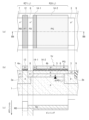
図2(a)及び(b)に示すように、第1導電型(p型)の基体領域1と、基体領域1の上部に埋め込まれた第2導電型(n型)の電荷生成埋込層5は、p-n接合によりフォトダイオード部PD(i,j)を構成する。フォトゲートPG(i,j)の透明電極を透過してフォトダイオード部PD(i,j)に光hνが入射することにより、フォトダイオード部PD(i,j)は信号電荷を生成する。また、電荷生成埋込層5の上面には、基体領域1よりも高不純物密度のp型のシールド層6が設けられている。シールド層6は、フォトゲート型の構造以外の光検出素子では「仮想電極」と呼ばれることがある。更に、シールド層6の上面には、フォトゲート絶縁膜(第1ゲート絶縁膜)4bと共にMOSキャパシタを構成する透明電極であるフォトゲートPG(i,j)が設けられている。図2(b)に示すように、リセットドレイン領域7、電荷読出領域8、電荷生成埋込層5、シールド層6及び接続領域3は、素子分離絶縁膜9によって額縁状に囲まれた活性領域の内部に収納されている。
2(a) and (b), the first conductive type (p-type)
素子分離絶縁膜9は、例えば浅溝分離(STI)構造によって、例えばシリコン酸化膜等で構成することが可能である。更に、図2(b)において、基体領域1よりも高不純物密度で第1導電型のウェル領域2a及び素子分離埋込領域2bが、基体領域1の上部の両側にそれぞれ埋め込まれている。製造工程を鑑みると、ウェル領域2aと同一の深さ、同一不純物密度で素子分離埋込領域2bが設けるのが好ましい。素子分離絶縁膜9と素子分離絶縁膜9の下を埋め込む素子分離埋込領域2bによって素子分離領域(画素分離領域)が構成されている。素子分離絶縁膜9によって囲まれた活性領域の内部において、リセットトランジスタRT(i,j)が、左側のウェル領域2aを用いて構成されている(図2(a)の表面図の表現ではリセットトランジスタRT(i,j)のゲート部分を「RT」と表示している。)。
The element
活性領域の範囲を規定する素子分離絶縁膜9は、基体領域1の右側に配置された素子分離埋込領域2bの上部の一部に埋め込まれている。また、素子分離埋込領域2bよりも高不純物密度のp+型の接続領域3が、素子分離埋込領域2bの上部の他の一部に素子分離絶縁膜9に接して設けられている。シールド層6は、右側の端部を素子分離埋込領域2bの上部で接続領域3に接され、左側の端部が電荷読出領域8に接続されるように、素子分離絶縁膜9で周辺を定義された活性領域の内部に配置されている。シールド層6の右側の端部は接続領域3を介して素子分離埋込領域2bに電気的に接続される。この結果、シールド層6の端部は接続領域3を介して基体領域1に電気的に短絡されて接地電位となる。
The element
リセットトランジスタRT(i,j)は、図2(a)及び(b)に示すように、電荷生成埋込層5よりも高不純物密度でn+型の電荷読出領域(リセットソース領域)8と、電荷生成埋込層5よりも高不純物密度でn+型のリセットドレイン領域7を備えている。更にリセットトランジスタRT(i,j)は、電荷読出領域8とリセットドレイン領域7の間のチャネル領域として機能するウェル領域2aの上面にリセットゲート絶縁膜(第2ゲート絶縁膜)4aを接し、絶縁膜・半導体界面を構成している。そして、リセットトランジスタRT(i,j)は、リセットゲート絶縁膜4aの上に、第2導電型(n+型)のDOPOSからなるリセットゲート電極12を備えている。図2(b)の例示的表現では、電荷読出領域8は、電荷生成埋込層5の端部の左側端部及びシールド層6の左側端部に接するように、活性領域の内部のウェル領域2aの上部及び基体領域1の上部に埋め込まれている。フォトゲートPG(i,j)は、リセットトランジスタRT(i,j)の電荷読出領域8側の端部に割り当てられた緩和領域部14-1と、電荷読出領域8側の反対側の接続領域3側に設けられた主透明電極層14-2の2つの領域に分割されている。連続した2つの領域に透明電極が分割されることにより、半導体界面の方向に沿って非一様に分布する静電ポテンシャルを生成する効果を奏している。緩和領域部14-1及び主透明電極層14-2のいずれも、入射光hνに対して透明な半導体電極であり、シールド層6に対して互いに異なる仕事関数の差を有している。
As shown in FIGS. 2A and 2B, the reset transistor RT(i,j) includes an n + type charge readout region (reset source region) 8 having a higher impurity density than the charge generation buried
第1実施形態に係る固体撮像装置では、半導体透明電極である緩和領域部14-1は、リセットトランジスタRT(i,j)のリセットゲート電極12と同じ第2導電型(n+型)の不純物元素を含む。一方、半導体透明電極である主透明電極層14-2は、リセットトランジスタRT(i,j)のリセットゲート電極12と逆の第1導電型(p+型)の不純物元素が添加されている。主透明電極層14-2は、透明電極であるフォトゲートPG(i,j)の主要部分を占め、その平面パターンで定義される面積(サイズ)は、図2(a)の平面パターンから分かるように緩和領域部14-1の面積よりも大きい。
In the solid-state imaging device according to the first embodiment, the relaxation region 14-1, which is a semiconductor transparent electrode, contains an impurity element of the second conductivity type (n + type) that is the same as that of the
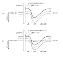
第1実施形態に係る光検出素子において、主透明電極層14-2の平面パターンの面積を、緩和領域部14-1の面積よりも大きく設定する理由を、フォトゲートPG(i,j)の透明電極が一様なn+DOPOSから構成される場合と一様なp+DOPOSから構成される場合に分けて説明する。但し、フォトゲートPG(i,j)の電位V(PG)は、基体領域1の電位(基板電位)と同じ0Vとする。図3(a)は、フォトゲートPG(i,j)の透明電極が一様な透明なn型半導体層である場合のフォトゲート光電変換部の伝導帯のバンド端Ec及び価電子帯のバンド端Evの深さ方向のプロファイルを示す。一方、図3(b)は、フォトゲートPG(i,j)の透明電極が一様な透明なp型半導体層である場合のフォトゲート光電変換部の伝導帯のバンド端Ec及び価電子帯のバンド端Evの深さ方向のプロファイルを示す。図3(a)及び(b)において、バンド中央の一点鎖線で示した曲線は、バンド中間点に位置する真性フェルミ準位Eiの深さ方向のプロファイルを示す。この時、図3(a)及び(b)に示すように、いずれの場合も、伝導帯のバンド端Ec、価電子帯のバンド端Ev及び真性フェルミ準位Eiを示す曲線が、電荷生成埋込層5を意味するn層のところで下に凸となるp-n-pフック構造をなしている。
In the photodetector according to the first embodiment, the reason for setting the area of the planar pattern of the main transparent electrode layer 14-2 larger than the area of the relaxation region 14-1 will be described separately for the case where the transparent electrode of the photogate PG(i,j) is made of uniform n + DOPOS and the case where it is made of uniform p + DOPOS. However, the potential V(PG) of the photogate PG(i,j) is set to 0 V, which is the same as the potential (substrate potential) of the
図3(a)及び(b)において、下に凸となる曲線でプロファイルを示した中央のn層の右側に示したp層(p基板)は基体領域1を意味し、n層の左側に示したp層は、シールド層6を意味している。シールド層6の更に左の平行四辺形はフォトゲート絶縁膜4bのバンド構造を示し、フォトゲート絶縁膜4bの更に左には、フォトゲートPG(i,j)の伝導帯のバンド端Ec及び価電子帯のバンド端Evを示している。図3(a)及び(b)のいずれの場合も、n層(電荷生成埋込層)の伝導帯のバンド端Ecを示す曲線が、フェルミレベルEf=0Vよりも下に位置して空乏化していることを示している。又、図3(a)及び(b)のいずれの場合も、p層(シールド層)の価電子帯のバンド端Evを示す曲線がフェルミレベルEf=0Vに近い位置に存在して中性化、即ち0Vにピンニングしている。
In Fig. 3(a) and (b), the p-layer (p-substrate) shown to the right of the central n-layer, whose profile is shown by a downwardly convex curve, means the
しかし、図3(a)に示すように、フォトゲートPG(i,j)の透明電極が一様なn+DOPOSで構成される場合には、シールド層6の伝導帯のバンド端Ec及び価電子帯のバンド端Evが、平行四辺形で示したフォトゲート絶縁膜4bとの半導体界面において、下向きに曲がっている。即ち、フォトゲートPG(i,j)の透明電極がn型の場合は、シールド層6のフォトゲートPG(i,j)側の半導体界面が僅かに空乏化する。図3(a)において、フォトゲート絶縁膜4bのバンド構造の左側にはn+DOPOSの伝導帯のバンド端EcがV(PG)=0Vに近づくことが示されている。n+DOPOSでフォトゲートPG(i,j)が構成される場合には、フォトゲートPG(i,j)側の真性フェルミ準位Eiとシールド層6の真性フェルミ準位Eiに差が生じて、フォトゲートPG(i,j) の仕事関数とシールド層6の仕事関数の間に差があるからである。
However, as shown in Fig. 3(a), when the transparent electrode of the photogate PG(i,j) is made of uniform n + DOPOS, the band edge Ec of the conduction band and the band edge Ev of the valence band of the
他方、フォトゲートPG(i,j)の透明電極が一様なp+DOPOSから構成される場合には、図3(b)に示すように、シールド層6の伝導帯のバンド端Ec及び価電子帯のバンド端Evが、平行四辺形で示したフォトゲート絶縁膜4bに向かって平坦なフラットバンドのプロファイルを維持している。図3(b)において、フォトゲート絶縁膜4bのバンド構造の左側にはp+DOPOSの価電子帯のバンド端EvがV(PG)=0Vに近づくことが示されている。p+DOPOSでフォトゲートPG(i,j)が構成される場合には、フォトゲートPG(i,j)側の真性フェルミ準位Eiとシールド層6の真性フェルミ準位Eiは、ほぼ同じレベルに出来るので、フォトゲートPG(i,j) の仕事関数とシールド層6の仕事関数の間の差は殆どない。更にp+DOPOSの不純物密度がシールドp層6の不純物密度より高密度であれば、シールド層6の真性フェルミ準位Eiの界面がやや上向きに引っ張られ、より一層ピンニング効果が高まる。
On the other hand, when the transparent electrode of the photogate PG(i,j) is made of uniform p + DOPOS, as shown in Fig. 3(b), the band edge Ec of the conduction band and the band edge Ev of the valence band of the
即ち、大きな仕事関数の差を伴うことなく、シールド層6の伝導帯のバンド端Ec及び価電子帯のバンド端Evが、深さ方向のフラットバンドのプロファイルを維持したまま、p-n-pフック構造の負方向に引っ張られるので、半導体界面には空乏化が生じない。図3(b)に示すような深さ方向の伝導帯のバンド端Ec及び価電子帯のバンド端Evが平坦なポテンシャル分布の形状では、シールド層6の半導体界面がシールド層6の多数キャリアである正孔(p型電荷)で埋められて強くピンニングしている。ピンニングされる正孔は、信号電荷である電子(n型電荷)とは逆極性の電荷である。
That is, without a large difference in work function, the band edge Ec of the conduction band and the band edge Ev of the valence band of the
したがって、シールド層6のフォトゲートPG(i,j)側の半導体界面における暗電流の発生については、半導体界面が多量の正孔で埋められるため不活性化されることを考慮すれば、フォトゲートPG(i,j)の透明電極が一様なp+DOPOSから構成される場合のほうが、フォトゲートPG(i,j)の透明電極が一様なn+DOPOSから構成される場合よりも抑えられることが分かる。半導体界面がシールド層6の多数キャリアである正孔(p型電荷)でピンニングされることは、放射線耐性に関しても、フォトゲートPG(i,j)の透明電極が一様なp+DOPOSから構成される場合のほうが、フォトゲートPG(i,j)の透明電極が一様なn+DOPOSから構成される場合よりも有利に働くことを意味する。なお、n層である電荷生成埋込層5に形成されるチャネル電位については、フォトゲートPG(i,j)の透明電極が一様なp+DOPOSから構成される場合、及び一様なn+DOPOSから構成される場合のいずれであっても、p層であるシールド層6が0Vにピンニングした状態を保持しているので、変わらない。
Therefore, considering that the semiconductor interface is inactivated because it is filled with a large number of holes, it is understood that the generation of dark current at the semiconductor interface on the photogate PG(i,j) side of the
以上の結果を考慮すると、図2(a)及び(b)に示すように、入射光hνに対して透明な半導体電極であるフォトゲートPG(i,j)の主透明電極層14-2をp型とし、リセットトランジスタRT(i,j)の電荷読出領域8側の緩和領域部14-1をn型とする構造は、面積を大きく設定した主透明電極層14-2における暗電流の発生を抑制するという効果の面で非常に優れたものとなる。また、暗電流抑制効果のみを考えると、透明電極であるフォトゲートPG(i,j)のすべてを一様なp型にすればよいとも考えられるが、透明電極のすべてを一様なp型として場合、図3(b)から明らかなように、フォトゲートPG(i,j)の電荷読出領域8側の端部において、シールド層6のフォトゲートPG(i,j)側の界面電位が強くピンニングする結果、一様なフォトゲートPG(i,j)と電荷読出領域8の間の電界集中を招き望ましくない。したがって、フォトゲートPG(i,j)を分割し、面積を大きく設定した主透明電極層14-2をp型とし、リセットトランジスタRT(i,j)の電荷読出領域8側の緩和領域部14-1をn型とする非一様な構造が最も理想的なものとなる。フォトゲートPG(i,j)の領域を複数の領域に分割してシールド層6に対して互いに異なる仕事関数の差をそれぞれ発生させ、半導体界面の方向に沿って非一様に分布する静電ポテンシャルを生成する効果を奏するという技術的特徴は、以下に述べる第2~第4実施形態に係る光検出器においても同様である。
Considering the above results, as shown in Figures 2(a) and (b), the structure in which the main transparent electrode layer 14-2 of the photogate PG(i,j), which is a semiconductor electrode transparent to the incident light hν, is p-type, and the relaxation region portion 14-1 on the
図2(b)に示した断面の方向に沿ったポテンシャル分布を、図2(c)に示す。図2(c)に示すように、リセットドレイン領域7の電位であるリセットドレイン電圧RDを、電荷生成埋込層5の空乏化電位より低い値に設定することにより、光電変換により発生した電荷を、電荷生成埋込層5及び電荷読出領域8に蓄積することができる。リセットドレイン電圧RDを空乏化電位より低くすることにより、信号電荷蓄積領域としての電荷生成埋込層5及び電荷読出領域8の電荷蓄積面積が電荷量Qsによらず一定に保たれ、電荷電圧変換ゲインを一定にすることができるという効果が得られる。なお、上述したように、電荷生成埋込層5に形成されるチャネル電位については、フォトゲートPG(i,j)の透明電極がp型であっても、n型であっても、シールド層6が0Vにピンニングした状態を保持しているので、変わることはなく等電位に保たれる。
The potential distribution along the direction of the cross section shown in FIG. 2(b) is shown in FIG. 2(c). As shown in FIG. 2(c), by setting the reset drain voltage RD, which is the potential of the
第1実施形態に係るフォトゲート型の光検出素子において、フォトゲートPG(i,j)は、フォトゲートPG(i,j)に入射する光hνの波長に対して透明な材料から選択することができる。例えば、フォトゲートPG(i,j)を燐(P)、砒素(As)等のn型の不純物元素がドープされたDOPOSから構成した場合、フォトゲートPG(i,j)と電荷読出領域8の位置合わせを自己整合的に行うことができるので、製造プロセス上便利となる。フォトゲートPG(i,j)は、DOPOS等の入射光hνの波長に対して透明な半導体の多結晶膜以外にも、 酸化錫(SnO2)でもよい。但し、錫(Sn)等を添加した酸化インジウム(ITO)は、Snがドナーとして働くのでn型になる。酸化錫は化学量論的組成に依存し、SnO2はn型、SnOはp型である。アルミニウム(Al)を添加した酸化亜鉛(AZO)、ガリウム(Ga)を添加した酸化亜鉛(GZO)、インジウム(In)を添加した酸化亜鉛(IZO)等の酸化物薄膜(透明導電性酸化物)等も化学量論的組成に依存するが、一般にn型半導体透明導電体である。
In the photogate type light detection element according to the first embodiment, the photogate PG(i,j) can be selected from materials transparent to the wavelength of light hν incident on the photogate PG(i,j). For example, when the photogate PG(i,j) is made of DOPOS doped with n-type impurity elements such as phosphorus (P) and arsenic (As), the photogate PG(i,j) and the
p型の透明導電体材料としては、ボロン(B)等のp型の不純物元素がドープされたDOPOSから構成するのが一般的であるが、シリコン以外に、酸化ニッケル(NiO)、酸化イリジウム(IrO)等が例示できる。更に、銅酸化アルミニウム(CuAlO2)、銅酸化ガリウム(CuGaO2)、銅酸化インジウム(CuInO2)等のCuMeO2デラフォサイト(Delafossite)構造を持つデラフォサイト型酸化物でもよい。CuFeO2:デラフォサイトは、Cu+とFeO2 -がc軸に垂直な2次元平面を構成し、これらが交互に積層した構造となっている。又、酸化銅ストロンチウム(SrCu2O2)、硫酸化銅ランタン(LaCuOS)等でもよい。「層状オキシカルコゲナイト:LnCuOCn」は、Ln=ランタニド、Ch=カルコゲナイト、Ln層とCuCh層がc軸に交互に積層されたものである。 The p-type transparent conductor material is generally composed of DOPOS doped with a p-type impurity element such as boron (B), but in addition to silicon, nickel oxide (NiO), iridium oxide (IrO), etc. can be exemplified. Furthermore, delafossite oxides having a CuMeO 2 delafossite structure such as copper aluminum oxide (CuAlO 2 ), copper gallium oxide (CuGaO 2 ), and copper indium oxide (CuInO 2 ) may be used. CuFeO 2 : Delafossite has a structure in which Cu + and FeO 2 - form a two-dimensional plane perpendicular to the c-axis, and these are alternately stacked. In addition, copper strontium oxide (SrCu 2 O 2 ), copper lanthanum sulfate (LaCuOS), etc. may be used. "Layered oxychalcogenide: LnCuOC n " is a compound in which Ln = lanthanide, Ch = chalcogenide, and Ln layers and CuCh layers are alternately laminated along the c-axis.
リセットゲート電極12についても、n+DOPOSから構成することにより、リセットゲート電極12と電荷読出領域8の位置合わせ、及びリセットゲート電極12とリセットドレイン領域7の位置合わせを自己整合的に行うことができるので、製造プロセス上便利となる。但し、フォトゲートPG(i,j)と同様に、リセットゲート電極12についても、i) 酸化錫(SnO2)、錫(Sn)等を添加した酸化インジウム(ITO)、ii) アルミニウム(Al)を添加した酸化亜鉛(AZO)、iii) ガリウム(Ga)を添加した酸化亜鉛(GZO)、iv) インジウム(In)を添加した酸化亜鉛(IZO)等の酸化物薄膜(透明導電性酸化物)から構成してもよい。
By forming the
フォトゲート絶縁膜4b及びリセットゲート絶縁膜4aとしては、単なるMOSトランジスタの場合のように、シリコン酸化膜に限定されるものではない。即ち、フォトゲート絶縁膜4b及びリセットゲート絶縁膜4aとしては、シリコン酸化膜の他、ストロンチウム酸化物(SrO)膜、シリコン窒化物(Si3N4)膜、アルミニウム酸化物(Al2O3)膜、マグネシウム酸化物(MgO)膜、イットリウム酸化物(Y2O3)膜、ハフニウム酸化物(HfO2)膜、ジルコニウム酸化物(ZrO2)膜、タンタル酸化物(Ta2O5)膜、ビスマス酸化物(Bi2O3)膜のいずれか1つの単層膜、或いはこれらの複数を積層した複合膜等を使用して、MISトランジスタを構成してもよい。但し、これらフォトゲート絶縁膜4b及びリセットゲート絶縁膜4aの材料としては、放射線に対して耐性があることが前提となる。
The photogate
図3(a)及び(b)では、基体領域1として、p型の半導体基板(Si基板)を用いる場合を例示しているが、半導体基板の代わりに、 i) p型の半導体基板上に、半導体基板よりも低不純物密度のp型のエピタキシャル成長層を形成して、エピタキシャル成長層を基体領域1として採用してもよく、ii) n型の半導体基板上に、n型のエピタキシャル成長層を形成して、エピタキシャル成長層を基体領域1として採用してもよく、iii) SOI構造のp型の半導体層(SOI層)を基体領域1として採用してもよい。
In Figs. 3(a) and (b), a p-type semiconductor substrate (Si substrate) is used as the
第1実施形態に係るフォトゲート型固体撮像装置の各画素Qijにおいては、電荷蓄積期間にフォトゲート光電変換部の光電変換により発生した信号電荷が、出力信号線Vsig(j)を介して読出回路50に読み出される。出力信号線Vsig(j)を介して読み出す時、透明電極であるフォトゲートPG(i,j)に0V近傍の一定値(DC値)であるフォトゲート電圧VPGを印加することにより、フォトゲートPG(i,j)のフォトゲート絶縁膜4bの直下のシールド層6の多数キャリアである正孔(ホール)でシールド層6の表面電位をピンニングすることができる。なお、緩和領域部14-1の直下のシールド層6の半導体界面部分と、主透明電極層14-2の直下のシールド層6の半導体界面部分でピンニングの状態が界面方向に沿って非一様に変化していることは、既に、図3(a)及び(b)で説明した通りである。
In each pixel Qij of the photogate type solid-state imaging device according to the first embodiment, a signal charge generated by photoelectric conversion of the photogate photoelectric conversion unit during a charge accumulation period is read out to the
第1実施形態に係る光検出素子によれば、X線やガンマ線等のイオン化放射線が照射されても、電荷生成埋込層5上のフォトゲート絶縁膜4bは4nm~10nm程度と薄いため、フォトゲート絶縁膜4b中に発生する電子正孔対は僅かである。従って、シールド層6の表面電位をピンニングすることによる暗電流の抑制効果と合わせて、耐放射線性能を向上させることができる。しかも、第1実施形態に係る光検出素子は、フォトゲートPG(i,j)の透明電極の主要部分をp型の主透明電極層14-2とし、リセットトランジスタRT(i,j)の電荷読出領域8側の端部をn型の緩和領域部14-1としている。よって、第1実施形態に係る光検出素子によれば、フォトゲートPG(i,j)と電荷読出領域8の間の電界集中を緩和しつつ、面積を大きく設定した主透明電極層14-2の直下のシールド層6の半導体界面の空乏化を抑え、暗電流抑圧を完全なものできる。したがって、第1実施形態に係る光検出素子を画素とした第1実施形態に係る固体撮像装置によれば、放射線環境下でも高感度かつ広ダイナミックレンジな撮像が可能になる。
According to the photodetector element of the first embodiment, even if ionizing radiation such as X-rays or gamma rays is irradiated, the
(第2実施形態)
本発明の第2実施形態に係る固体撮像装置についても、回路構成としては第1実施形態と基本的に同じである。即ち、第2実施形態に係る固体撮像装置は、図1に例示した構成と同様に、複数のフォトゲート型の画素Qijが二次元マトリクス状に配列された画素領域と、画素領域の周辺に配置され、RT走査回路20、SL走査回路30、及びPG走査回路40を含む周辺回路を備えている。第2実施形態に係る固体撮像装置の画素領域の内部の回路構成については、第1実施形態と同じであるので、重複する説明を省略し、二次元マトリクスを構成する画素である光検出素子の構造に注目して説明する。
Second Embodiment
The circuit configuration of the solid-state imaging device according to the second embodiment of the present invention is also basically the same as that of the first embodiment. That is, the solid-state imaging device according to the second embodiment includes a pixel region in which a plurality of photogate type pixels Qij are arranged in a two-dimensional matrix, and peripheral circuits arranged around the pixel region and including an
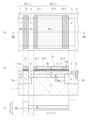
第2実施形態に係る光検出素子が、第1実施形態で説明した光検出素子10と異なる点は、光検出素子内の入射光hνに対して透明な半導体電極であるフォトゲートPG(i,j)の構造にある。光検出素子は、図4(a)及び(b)に示すように、電荷生成部として機能するフォトダイオード部PD(i,j)と、フォトゲートPG(i,j)と、リセットトランジスタRT(i,j)を備える。図4(a)に示す平面パターンにおいて、フォトゲートPG(i,j)とリセットトランジスタRT(i,j)は横並びに配置されている。リセットトランジスタRT(i,j)のリセットゲートRTを示す帯状のパターンの一方側(右側)、即ち、透明電極であるフォトゲートPG(i,j)側には、FDで示した電荷読出領域(電荷検出部)8が配置され、リセットゲートRTの他方側(左側)にはRDで示したリセットドレイン領域7が配置されている。
The photodetector according to the second embodiment differs from the
図4(b)に示すように、第1導電型(p型)の基体領域1と基体領域1の上部に埋め込まれた第2導電型(n型)の電荷生成埋込層5は、p-n接合によりフォトダイオード部PD(i,j)を構成する。フォトゲートPG(i,j)の透明電極を透過してフォトダイオード部PD(i,j)に光hνが入射することにより、フォトダイオード部PD(i,j)は信号電荷を生成する。図4(a)に示した電荷読出領域FDは、基体領域1の内部においてフォトダイオード部PD(i,j)を構成する第2導電型(n型)の電荷生成埋込層5に接続されている。また、電荷生成埋込層5の上面には、基体領域1よりも高不純物密度のp型のシールド層6が設けられている。
As shown in FIG. 4(b), the first conductive type (p-type)
そして、シールド層6の上面にフォトゲート絶縁膜(第1ゲート絶縁膜)4bが接して設けられることにより、シールド層6と絶縁膜・半導体界面が構成されている。そして、フォトゲート絶縁膜4bの上には入射光hνに対して透明な半導体電極であるフォトゲートPG(i,j)が設けられている。図4(a)に示すように、リセットドレイン領域7、電荷読出領域8、電荷生成埋込層5及び接続領域3は、素子分離絶縁膜9によって額縁状に囲まれた活性領域の敷地内に配置されている。図4(b)を見れば、シールド層6及び電荷生成埋込層5も、素子分離絶縁膜9によって周辺が定義された活性領域内に配置されていることが分かる。素子分離絶縁膜9は、例えばSTI構造によって、シリコン酸化膜等で構成することが可能である。
The photogate insulating film (first gate insulating film) 4b is provided on the upper surface of the
更に、図4(b)において、基体領域1よりも高不純物密度で第1導電型のウェル領域2a及び素子分離埋込領域2bが、基体領域1の上部の両側の位置にそれぞれ埋め込まれている。製造工程を鑑みると、ウェル領域2aと同一の深さ、同一不純物密度で素子分離埋込領域2bを設けて構わない。素子分離絶縁膜9と素子分離絶縁膜9の下を埋め込む素子分離埋込領域2bによって素子分離領域(画素分離領域)が構成される。
In addition, in FIG. 4(b), a first conductivity
リセットトランジスタRT(i,j)は、左側のウェル領域2a内に設けられている。活性領域の範囲を規定する素子分離絶縁膜9は、基体領域1の右側に配置された素子分離埋込領域2bの上部の一部に埋め込まれている。また、素子分離埋込領域2bよりも高不純物密度のp+型の接続領域3が、素子分離埋込領域2bの上部の他の一部に素子分離絶縁膜9に接して設けられている。よって、接続領域3も活性領域の内部に位置する。シールド層6も、活性領域の内部に位置するように、素子分離埋込領域2bの上部において接続領域3に接して設けられている。シールド層6の右側の端部が接続領域3を介して素子分離埋込領域2bに電気的に接続されるので、シールド層6は接続領域3を介して基体領域1に電気的に短絡されて接地電位となる。
The reset transistor RT(i,j) is provided in the
リセットトランジスタRT(i,j)は、電荷生成埋込層5よりも高不純物密度のn+型の電荷読出領域8をリセットソース領域として備え、更に電荷生成埋込層5よりも高不純物密度のn+型のリセットドレイン領域7を備えている。更にリセットトランジスタRT(i,j)は、電荷読出領域8とリセットドレイン領域7の間のチャネル領域として機能するウェル領域2aの上面にリセットゲート絶縁膜(第2ゲート絶縁膜)4aを接し、絶縁膜・半導体界面を構成している。そして、リセットゲート絶縁膜4aの上には第2導電型(n+型)のDOPOSからなるリセットゲート電極12を備えている。電荷読出領域8は、電荷生成埋込層5の端部及びシールド層6の端部に接するように、ウェル領域2aの上部の一部と基体領域1の上部の一部に埋め込まれている。
The reset transistor RT(i,j) includes an n + type
フォトゲートPG(i,j)の透明電極は、リセットトランジスタRT(i,j)の電荷読出領域8側となる左側端部に割り当てられた緩和領域部14-1と、接続領域3側となる右側端部に割り当てられた抵抗増大部14-3と、緩和領域部14-1と抵抗増大部14-3間に設けられた主透明電極層14-2の3つの領域に分割されている。連続した3つの領域に透明電極が分割されることにより、半導体界面の方向に沿って非一様に分布する静電ポテンシャルを生成する効果を奏している。図4(a)に示す平面パターンにおいては、左側の緩和領域部14-1と右側の抵抗増大部14-3は、互いに平行に対向する帯状のパターンとなっている。
The transparent electrode of the photogate PG(i,j) is divided into three regions: a relaxation region 14-1 allocated to the left end portion on the
第2実施形態に係る光検出器では、半導体透明電極である緩和領域部14-1及び抵抗増大部14-3は、リセットトランジスタRT(i,j)のリセットゲート電極12と同じ第2導電型(n+型)の不純物元素が添加されたDOPOSである。一方、半導体透明電極である主透明電極層14-2は、リセットゲート電極12と逆の第1導電型(p+型)の不純物元素が添加されたDOPOSである。このため、抵抗増大部14-3と主透明電極層14-2の間、及び主透明電極層14-2と緩和領域部14-1の間にそれぞれp-n接合が構成される。また、主透明電極層14-2は、透明電極であるフォトゲートPG(i,j)の主要部分を占め、その平面パターンで定義される面積(サイズ)は、緩和領域部14-1の面積及び抵抗増大部14-3の面積よりも大きい。また、透明電極であるフォトゲートPG(i,j)に印加する電圧は、抵抗増大部14-3を入力端とし、抵抗増大部14-3から主透明電極層14-2を経由して緩和領域部14-1に供給される。
In the photodetector according to the second embodiment, the relaxation region 14-1 and the resistance increase region 14-3, which are semiconductor transparent electrodes, are made of DOPOS doped with an impurity element of the same second conductivity type (n + type) as the
主透明電極層14-2を第1導電型(p+型)としているので、シールド層6の半導体表面(半導体界面)との間の仕事関数差により、シールド層6の半導体表面がより強く、シールド層6の多数キャリアである正孔でピニングされることは第1実施形態に係る光検出器と同様である。ピンニングされる正孔(p型電荷)は、信号電荷である電子(n型電荷)とは逆極性の電荷である。半導体表面(半導体界面)の正孔が強くピンニングされるので、第2実施形態に係る光検出器を画素として固体撮像装置を構成すれば、半導体界面を多量の正孔で埋めて不活性化して暗電流の抑圧を完全化でき、放射線環境下でも高感度かつ広ダイナミックレンジな撮像が可能となる。また、緩和領域部14-1を第2導電型(n+型)とすることにより、フォトゲートPG(i,j)と電荷読出領域8の間の電界集中を緩和することが可能となる。更に、第2導電型(n+型)の抵抗増大部14-3を、フォトゲートPG(i,j)に印加する電圧を与える入力端とすることで、抵抗増大部14-3から緩和領域部14-1までには2つのp-n接合が存在し、抵抗増大部14-3から緩和領域部14-1までの電気経路の抵抗が大きくなる。抵抗増大部14-3から主透明電極層14-2を経て緩和領域部14-1までの電気経路の抵抗が増大することにより、フォトゲートPG(i,j)と電荷読出領域8の間の電界集中を更に緩和することができる。
Since the main transparent electrode layer 14-2 is of the first conductivity type (p + type), the semiconductor surface of the
図4(b)に示した断面の方向に沿ったポテンシャル分布を、図4(c)に示す。第2実施形態に係る光検出器では、リセットドレイン領域7の電位であるリセットドレイン電圧RDを電荷生成埋込層5の空乏化電位より低い値に設定し、光電変換により発生した電荷を電荷生成埋込層5及び電荷読出領域8に蓄積する。リセットドレイン電圧RDを電荷生成埋込層5の空乏化電位より低い値に設定することにより、信号電荷蓄積領域としての電荷生成埋込層5及び電荷読出領域8の電荷蓄積面積が電荷量Qsによらず一定に保たれ、電荷電圧変換ゲインを一定にすることができるという効果が得られる。なお、電荷生成埋込層5に形成されるチャネル電位については、フォトゲートPG(i,j)の透明電極がp型であっても、n型であっても、シールド層6が0Vにピンニングした状態を保持しているので、変わることはなく等電位に保たれる。
The potential distribution along the direction of the cross section shown in FIG. 4(b) is shown in FIG. 4(c). In the photodetector according to the second embodiment, the reset drain voltage RD, which is the potential of the
第2実施形態に係る光検出器においても、X線やガンマ線等のイオン化放射線が照射されても、電荷生成埋込層5上のフォトゲート絶縁膜4bは4nm~10nm程度と薄いため、フォトゲート絶縁膜4b中に発生する電子正孔対は僅かである。従って、シールド層6の表面電位をピンニングすることによる暗電流の抑制効果と合わせて、耐放射線性能を向上させることができる。しかも、フォトゲートPG(i,j)の透明電極の主要部分をp型の主透明電極層14-2とし、リセットトランジスタRT(i,j)の電荷読出領域8側の端部をn型の緩和領域部14-1とし、更に接続領域3側の端部をn型の抵抗増大部14-3としている。図3(a)及び(b)で説明した通り、緩和領域部14-1及び抵抗増大部14-3の直下のシールド層6の半導体界面部分と、主透明電極層14-2の直下のシールド層6の半導体界面部分では、ピンニングの状態が界面方向に沿って非一様に変化している。このため、第2実施形態に係る光検出器によれば、フォトゲートPG(i,j)と電荷読出領域8の間の電界集中を緩和しつつ、面積を大きく設定した主透明電極層14-2の直下のシールド層6の半導体界面の空乏化を抑えることができ、暗電流抑圧を完全なものにできる。したがって、3つの領域に透明電極を分割した第2実施形態に係る光検出器を画素として、第2実施形態に係る固体撮像装置を構成すれば、暗電流が抑圧され、放射線環境下でも高感度かつ広ダイナミックレンジな撮像が可能になる。
Even in the photodetector according to the second embodiment, even if ionizing radiation such as X-rays or gamma rays is irradiated, the
(第3実施形態)
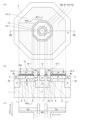
本発明の第3実施形態に係る固体撮像装置は、第1実施形態に係る固体撮像装置の応用例に対応する。第3実施形態に係る固体撮像装置を構成する画素として機能する光検出素子は、第1実施形態に係る光検出素子の平面レイアウトに対し工夫を加えている。即ち、第3実施形態に係る光検出素子は、ガンマ線照射により劣化し易い、シリコン酸化膜等の素子分離絶縁膜を、電荷生成埋込層5から遠ざけることで、放射線耐性をより一層高める。このため、第3実施形態に係る光検出器では、フォトゲートPG(i,j)及び電荷読出領域FDの平面レイアウトがいずれも同心環状であり、平面レイアウトの中央部に環状のリセットゲート電極12を有するリセットトランジスタRT(i,j)を配置している。図5(a)及び(b)に例示する第3実施形態に係る光検出器では、フォトゲートPG(i,j)及び電荷読出領域FDの平面レイアウトをいずれも八角形リング状とし、フォトゲートPG(i,j)の中央部に八角形リング状のリセットゲート電極12を有するリセットトランジスタRT(i,j)を配置している。
Third Embodiment
The solid-state imaging device according to the third embodiment of the present invention corresponds to an application example of the solid-state imaging device according to the first embodiment. The photodetecting elements functioning as pixels constituting the solid-state imaging device according to the third embodiment are modified in planar layout from the photodetecting element according to the first embodiment. That is, the photodetecting element according to the third embodiment further enhances radiation resistance by moving the element isolation insulating film such as a silicon oxide film, which is easily deteriorated by gamma ray irradiation, away from the charge generation buried
図1の光検出素子に相当する部分は、図5(a)及び(b)に示すように、電荷生成部であるフォトダイオード部PD(i,j)と、フォトゲートPG(i,j)と、リセットトランジスタRT(i,j)を備える。フォトゲートPG(i,j)は、リセットトランジスタRT(i,j)を環状に取り囲むレイアウトを有している。リセットトランジスタRT(i,j)のリセットゲートRTの外周側、即ち、透明電極であるフォトゲートPG(i,j)側には、FDで示した電荷読出領域(電荷検出部)8が配置され、内周側には、RDで示したリセットドレイン領域7が配置されている。図5(a)及び(b)に示すように、第3実施形態に係る光検出器は、RDで示したリセットドレイン領域7を中心として、これを八角形リング状のリセットゲート電極12が取り囲み、更に、リセットゲート電極12を電荷読出領域FD及びフォトゲートPG(i,j)が取り囲むレイアウトを有している。
As shown in FIGS. 5(a) and (b), the part corresponding to the photodetector element in FIG. 1 includes a photodiode portion PD(i,j) which is a charge generating portion, a photogate PG(i,j), and a reset transistor RT(i,j). The photogate PG(i,j) has a layout that surrounds the reset transistor RT(i,j) in a ring shape. A charge readout region (charge detection portion) 8 indicated by FD is arranged on the outer periphery side of the reset gate RT of the reset transistor RT(i,j), that is, on the side of the photogate PG(i,j) which is a transparent electrode, and a
図5(b)から分かるように、第1導電型(p型)の基体領域1と、基体領域1の上部の一部に埋め込まれた第2導電型(n型)の電荷生成埋込層5は、p-n接合によりフォトダイオード部PD(i,j)を構成する。フォトゲートPG(i,j)の透明電極を透過してフォトダイオード部PD(i,j)に光hνが入射することにより、フォトダイオード部PD(i,j)は信号電荷を生成する。図5(a)に示した電荷読出領域FDは、基体領域1の内部において電荷生成埋込層5に接続されている。また、基体領域1の上部の他の一部となる電荷生成埋込層5の上面には、基体領域1よりも高不純物密度のp型のシールド層6が設けられている。電荷生成埋込層5及びシールド層6は、例えば、八角形リング状等の環状を有している。シールド層6の上面にはフォトゲート絶縁膜(第1ゲート絶縁膜)4bが接して設けられ、絶縁膜・半導体界面が構成されている。
As can be seen from FIG. 5(b), the first conductive type (p type)
そして、シールド層6の上方となるフォトゲート絶縁膜4bの上には入射光hνに対して透明な半導体電極であるフォトゲートPG(i,j)が設けられている。また、基体領域1の上部となる中央部には、基体領域1よりも高不純物密度で第1導電型のウェル領域2aが埋め込まれている。更に、基体領域1の上部となる周辺部には、基体領域1よりも高不純物密度で第1導電型の素子分離埋込領域2bが埋め込まれている。製造工程を鑑みると、ウェル領域2aと同一の深さ、同一不純物密度で素子分離埋込領域2bを埋め込んでも構わない。リセットトランジスタRT(i,j)は、中央部のウェル領域2aの上部の一部に設けられている。更に、素子分離埋込領域2bよりも高不純物密度のp+型の接続領域3が外周側に設けられた素子分離埋込領域2bの上部の一部に設けられている。シールド層6は、素子分離埋込領域2b内の接続領域3に接して、基体領域1の上部の一部に設けられている。シールド層6の外周側の端部が接続領域3を介して素子分離埋込領域2bに電気的に接続されるので、シールド層6は接続領域3を介して基体領域1に電気的に短絡されて接地電位となる。
A photogate PG(i,j) which is a semiconductor electrode transparent to incident light hν is provided on the
図5(a)及び(b)では図示を省略しているが、正八角形の接続領域3を囲むように、更に外側となる基体領域1の上部には素子分離絶縁膜が配置されている。素子分離絶縁膜(図示省略)と素子分離絶縁膜の下を埋め込む素子分離埋込領域2bによって素子分離領域(画素分離領域)が構成される。第1及び第2実施形態に係る固体撮像装置と同様に、素子分離絶縁膜は、例えばSTI構造によって基体領域1の上部に埋め込むことが可能である。第3実施形態に係る光検出器では、素子分離絶縁膜(図示省略)が、光検出素子の最も外周側に位置する第1導電型の素子分離埋込領域2b又は接続領域3の、更に外側に存在するレイアウトを採用しているので、フォトゲート型固体撮像装置の各画素のそれぞれの放射線耐性を高めることができる。
Although not shown in FIGS. 5A and 5B, an element isolation insulating film is arranged on the top of the
第3実施形態に係る光検出器のリセットトランジスタRT(i,j)は、電荷生成埋込層5よりも高不純物密度のn+型のリセットドレイン領域7を、中央部のウェル領域2aの上部の中心に配置している。更に、図5(b)に示すように、電荷生成埋込層5よりも高不純物密度のn+型の電荷読出領域8をリセットドレイン領域7から離間して配置している。電荷読出領域8は、ウェル領域2aの上部の周辺部と、基体領域1の上部の一部に、ウェル領域2aの上部の周辺部から張り出すように埋め込んでいる。そして、リセットトランジスタRT(i,j)は、電荷読出領域8とリセットドレイン領域7の間に形成されるチャネル領域となるウェル領域2aの上部の一部が露出した箇所の上にリセットゲート絶縁膜(第2ゲート絶縁膜)4aを接し、絶縁膜・半導体界面を構成している。更に、図5(b)に示すように、リセットゲート絶縁膜4aの上に第2導電型(n+型)のDOPOSからなるリセットゲート電極12を配置している。
In the reset transistor RT(i,j) of the photodetector according to the third embodiment, an n + type reset drain region 7 having a higher impurity density than the charge generation buried layer 5 is disposed at the center of the upper part of the central well region 2a. Furthermore, as shown in FIG. 5B, an n+ type
図5(a)に示すように、電荷読出領域8は、リセットドレイン領域7を中心とする、例えば八角形リング状等の環状を有している。そして図5(b)に示すように、電荷生成埋込層5の内径側端部及びシールド層6の内径側端部に接して電荷読出領域8が埋め込まれている。電荷読出領域8が八角形リング状であれば、入射光hνに対して透明な半導体電極であるフォトゲートPG(i,j)も八角形リング状等の環状を有することが好ましい。フォトゲートPG(i,j)の透明電極は、図5(a)に示すようにリセットトランジスタRT(i,j)の電荷読出領域8側の端部に割り当てられた内周側の緩和領域部14-1と、緩和領域部14-1を囲んで主要部分として設けられた主透明電極層14-2の2つの領域に分割されている。連続した2つの領域に透明電極が分割されることにより、半導体界面の方向に沿って非一様に分布する静電ポテンシャルを生成する効果を奏している。
As shown in FIG. 5(a), the
第3実施形態に係る光検出器では、第1実施形態と同様に、半導体透明電極である内周側の緩和領域部14-1は、リセットトランジスタRT(i,j)のリセットゲート電極12と同じ第2導電型(n+型)の不純物元素が添加されたDOPOSである。一方、半導体透明電極である主透明電極層14-2は、リセットトランジスタRT(i,j)のリセットゲート電極12と逆の第1導電型(p+型)の不純物元素が添加されたDOPOSである。また、主透明電極層14-2は、透明電極であるフォトゲートPG(i,j)の主要部分としての機能をなすものであるので、その平面パターンで定義される面積(サイズ)は、緩和領域部14-1の面積よりも大きい。既に、図3(a)及び(b)で説明した通り、緩和領域部14-1の直下のシールド層6の半導体界面部分と、主透明電極層14-2の直下のシールド層6の半導体界面部分では、ピンニングの状態が界面方向に沿って非一様に変化している。
In the photodetector according to the third embodiment, similarly to the first embodiment, the relaxation region 14-1 on the inner periphery side, which is a semiconductor transparent electrode, is DOPOS doped with an impurity element of the same second conductivity type (n + type) as the
主透明電極層14-2を第1導電型(p+型)としているので、シールド層6の半導体表面(半導体界面)との間の仕事関数差により、シールド層6の半導体表面がより強く、シールド層6の多数キャリアである正孔でピニングされる現象は、第1実施形態に係る光検出素子と同様である。ピンニングされる正孔(p型電荷)は、信号電荷である電子(n型電荷)とは逆極性の電荷である。正孔のピンニングにより半導体界面を多量の正孔で埋めることにより暗電流を不活性化できるので、この光検出素子を各画素として配列した個体撮像装置は、放射線環境下でも高感度かつ広ダイナミックレンジな撮像が可能となる。また、緩和領域部14-1を第2導電型(n+型)とすることにより、フォトゲートPG(i,j)と電荷読出領域8の間の電界集中を緩和することが可能となる。更に、リセットドレイン領域7を中心にして、リセットゲート電極12、フォトゲートPG(i,j)、及び電荷読出領域FDがそれぞれ同心環状となるような平面レイアウトを有している。したがって、第3実施形態に係る固体撮像装置は、各画素の内部において、ガンマ線照射により劣化し易い素子分離絶縁膜が電荷生成埋込層5から遠い構造が容易に実現され、放射線耐性をより一層高めることができる。
Since the main transparent electrode layer 14-2 is of the first conductivity type (p + type), the semiconductor surface of the
図5(b)に示した断面の方向に沿ったポテンシャル分布を、図5(c)に示す。図5(c)において、リセットドレイン領域7の電位であるリセットドレイン電圧RDを電荷生成埋込層5の空乏化電位より低い値に設定することにより、光電変換により発生した電荷を電荷生成埋込層5及び電荷読出領域8に蓄積することができる。リセットドレイン電圧RDを空乏化電位より低い値に設定することにより、信号電荷蓄積領域としての電荷生成埋込層5及び電荷読出領域8の電荷蓄積面積が電荷量Qsによらず一定に保たれ、電荷電圧変換ゲインを一定にすることができるという効果が得られる。なお、電荷生成埋込層5に形成されるチャネル電位については、フォトゲートPG(i,j)の透明電極がp型であっても、n型であっても、シールド層6が0Vにピンニングした状態を保持しているので、変わることはなく等電位に保たれる。
The potential distribution along the direction of the cross section shown in FIG. 5(b) is shown in FIG. 5(c). In FIG. 5(c), the reset drain voltage RD, which is the potential of the
第3実施形態に係る光検出器においては、第1実施形態に係る光検出器と同様の効果、即ち、フォトゲートPG(i,j)と電荷読出領域8の間の電界集中を緩和しつつ、面積を大きく設定した主透明電極層14-2の直下のシールド層6の半導体界面の空乏化を抑え、暗電流抑圧を完全なものとすることができる。したがって第3実施形態に係る固体撮像装置によれば、放射線環境下でも高感度かつ広ダイナミックレンジな撮像を可能にする有利な効果を奏することができる。しかも、リセットドレイン領域7を中心にして、リセットゲート電極12、フォトゲートPG(i,j)、及び電荷読出領域FDが、それぞれ同心環状に囲む平面レイアウトの画素構造であるので、各画素の内部において、ガンマ線照射により劣化し易い素子分離絶縁膜を電荷生成埋込層5から遠ざけ、放射線耐性をより一層高めることができる。
The photodetector according to the third embodiment has the same effect as the photodetector according to the first embodiment, that is, it is possible to suppress depletion of the semiconductor interface of the
(第4実施形態)
本発明の第4実施形態に係る固体撮像装置は、第2実施形態に係る固体撮像装置の応用例に対応する。即ち、第2実施形態に係る固体撮像装置の各画素としてそれぞれ機能する光検出素子の平面レイアウトに対し工夫を加えている。第4実施形態に係る光検出素子は、ガンマ線照射により劣化し易い、シリコン酸化膜等の素子分離絶縁膜を電荷生成埋込層5から遠ざけることで、放射線耐性をより一層高め得る構造を提供する。即ち、第4実施形態に係る光検出器では、フォトゲートPG(i,j)及び電荷読出領域FDの平面レイアウトがいずれも同心環状であり、その中央部に環状のリセットゲート電極12を有するリセットトランジスタRT(i,j)を配置している。図6(a)及び(b)に示すように、フォトゲートPG(i,j)及び電荷読出領域FDの平面レイアウトが八角形リング状の場合は、その中央部に八角形リング状のリセットゲート電極12を有するリセットトランジスタRT(i,j)を配置するのが好ましい。
Fourth Embodiment
The solid-state imaging device according to the fourth embodiment of the present invention corresponds to an application example of the solid-state imaging device according to the second embodiment. That is, the planar layout of the photodetecting elements that function as each pixel of the solid-state imaging device according to the second embodiment is devised. The photodetecting element according to the fourth embodiment provides a structure that can further improve radiation resistance by moving the element isolation insulating film such as a silicon oxide film, which is easily deteriorated by gamma ray irradiation, away from the charge generation buried
図6(a)及び(b)に示すように、第4実施形態に係る光検出器は、電荷生成部であるフォトダイオード部PD(i,j)と、フォトゲートPG(i,j)と、リセットトランジスタRT(i,j)を備える点では図1に示した第1実施形態に係る光検出器と同様である。しかし、第1実施形態に係る光検出器とは異なり、フォトゲートPG(i,j)は、中心に位置するリセットトランジスタRT(i,j)を環状に取り囲むレイアウトを有している。リセットトランジスタRT(i,j)のリセットゲートRTの外周側、即ち、透明電極であるフォトゲートPG(i,j)側には、図6(a)にFDで示した電荷読出領域(電荷検出部)8が配置され、内周側には、RDで示したリセットドレイン領域7が配置されている。
As shown in Figs. 6(a) and (b), the photodetector according to the fourth embodiment is similar to the photodetector according to the first embodiment shown in Fig. 1 in that it includes a photodiode portion PD(i,j) which is a charge generating portion, a photogate PG(i,j), and a reset transistor RT(i,j). However, unlike the photodetector according to the first embodiment, the photogate PG(i,j) has a layout that surrounds the reset transistor RT(i,j) located at the center in an annular shape. A charge readout region (charge detection portion) 8 indicated by FD in Fig. 6(a) is arranged on the outer periphery of the reset gate RT of the reset transistor RT(i,j), i.e., on the side of the photogate PG(i,j) which is a transparent electrode, and a
図6(b)に示すように、第1導電型(p型)の基体領域1と、基体領域1の上部の一部に埋め込まれた第2導電型(n型)の電荷生成埋込層5は、p-n接合によりフォトダイオード部PD(i,j)を構成する。フォトゲートPG(i,j)の透明電極を透過してフォトダイオード部PD(i,j)に光hνが入射することにより、フォトダイオード部PD(i,j)は信号電荷を生成する。電荷読出領域FDは、基体領域1の内部において電荷生成埋込層5に接続されている。また、電荷生成埋込層5の上面となる基体領域1には、基体領域1よりも高不純物密度のp型のシールド層6が埋め込まれている。電荷生成埋込層5及びシールド層6は、例えば、八角形リング状等の環状を有している。シールド層6の上面にはフォトゲート絶縁膜(第1ゲート絶縁膜)4bが接して設けられ、シールド層6と絶縁膜・半導体界面が構成されている。そして、シールド層6の上方の位置において、フォトゲート絶縁膜4bの上には入射光hνに対して透明な半導体電極であるフォトゲートPG(i,j)が設けられている。
As shown in FIG. 6(b), the first conductive type (p-type)
また、基体領域1の上部となる中央部には、基体領域1よりも高不純物密度で第1導電型のウェル領域2aが埋め込まれ、基体領域1の上部となる周辺部には、基体領域1よりも高不純物密度で第1導電型の素子分離埋込領域2bが埋め込まれている。リセットトランジスタRT(i,j)は、ウェル領域2aの上部の一部に設けられている。更に、素子分離埋込領域2bよりも高不純物密度のp+型の接続領域3が素子分離埋込領域2bの上部に埋め込まれている。素子分離埋込領域2bは、ウェル領域2aと同一の深さ、同一不純物密度で構わない。シールド層6は、素子分離埋込領域2b内の接続領域3に接し、素子分離埋込領域2b内から内側の基体領域1の上部に張り出すように環状に設けられている。シールド層6の外周側の端部が接続領域3を介して素子分離埋込領域2bに電気的に接続されるので、シールド層6は接続領域3を介して基体領域1に電気的に短絡されて接地電位となる。
In addition, a first
図6(a)及び(b)では図示を省略しているが、正八角形の接続領域3を囲むように、更に外側となる基体領域1の上部には素子分離絶縁膜が配置されている。素子分離絶縁膜(図示省略)と素子分離絶縁膜の下を埋め込む素子分離埋込領域2bによって素子分離領域(画素分離領域)が構成される。第1~第3実施形態に係る光検出器と同様に、素子分離絶縁膜は、例えばSTI構造によって基体領域1の上部に埋め込むことが可能である。図6(a)及び(b)に示すように、第4実施形態に係る光検出器を構成する画素となる光検出素子は、RDで示したリセットドレイン領域7を中心として、これを八角形リング状のリセットゲート電極12が取り囲み、更に、リセットゲート電極12を、電荷読出領域FD及びフォトゲートPG(i,j)が取り囲むレイアウトを有している。第4実施形態に係る光検出器では、素子分離絶縁膜(図示せず)は、最も外周の素子分離埋込領域2b又は接続領域3の外側に存在する構造を採用しているので、フォトゲート型固体撮像装置を構成する各画素のそれぞれの放射線耐性を高めることができる。
Although not shown in FIGS. 6(a) and (b), an element isolation insulating film is arranged on the top of the
第4実施形態に係る光検出器のリセットトランジスタRT(i,j)は、電荷生成埋込層5よりも高不純物密度のn+型のリセットドレイン領域7を、中央部のウェル領域2aの上部の中心に配置している。更に、リセットトランジスタRT(i,j)は、電荷生成埋込層5よりも高不純物密度のn+型の電荷読出領域8をリセットソース領域として、リセットドレイン領域7から離間して配置している。電荷読出領域8は、ウェル領域2aの上部の周辺部と、基体領域1の上部の一部に、ウェル領域2aの上部の周辺部から外周側に張り出すように埋め込んでいる。そして、リセットトランジスタRT(i,j)は、電荷読出領域8とリセットドレイン領域7の間に形成されるチャネル領域となるウェル領域2aの上部の一部が露出した箇所の上にリセットゲート絶縁膜(第2ゲート絶縁膜)4aを接し、絶縁膜・半導体界面を構成している。更に、リセットトランジスタRT(i,j)は、リセットゲート絶縁膜4aの上に第2導電型(n+型)のDOPOSからなるリセットゲート電極12を配置している。
In the reset transistor RT(i,j) of the photodetector according to the fourth embodiment, an n + type reset drain region 7 having a higher impurity density than the charge generation buried layer 5 is disposed at the center of the upper part of the central well region 2a. Furthermore, the reset transistor RT(i,j) has an n+ type
図6(a)に例示したように、電荷読出領域8は、八角形リング状等の環状の形状で、リセットドレイン領域7を囲んでいる。図6(b)に示すように、電荷読出領域8は、基体領域1の内部において、電荷生成埋込層5の内径側端部及びシールド層6の内径側端部に接し、ウェル領域2aの上部から周辺の基体領域1の上部に渡る領域の一部に環状に埋め込まれている。フォトゲートPG(i,j)は、例えば、八角形リング状等の環状を有し、リセットトランジスタRT(i,j)の電荷読出領域8側の端部に割り当てられた内周側の緩和領域部14-1と、接続領域3側の端部に割り当てられた抵抗増大部14-3と、これら緩和領域部14-1及び抵抗増大部14-3間に設けられた主透明電極層14-2の3つの領域に分割されている。連続した3つの領域に透明電極が分割されることにより、半導体界面の方向に沿って非一様に分布する静電ポテンシャルを生成する効果を奏している。図3(a)及び(b)の説明から分かるように、緩和領域部14-1及び抵抗増大部14-3のそれぞれの直下のシールド層6の半導体界面部分と、主透明電極層14-2の直下のシールド層6の半導体界面部分でピンニングの状態が異なる。
As shown in FIG. 6(a), the
本発明の第4実施形態に係る光検出器では、第2実施形態に係る光検出器と同様に、緩和領域部14-1及び抵抗増大部14-3は、リセットトランジスタRT(i,j)のリセットゲート電極12と同じ第2導電型(n+型)の不純物元素が添加されたDOPOSである。一方、主透明電極層14-2は、リセットトランジスタRT(i,j)のリセットゲート電極12と逆の第1導電型(p+型)の不純物元素が添加されたDOPOSである。このため、緩和領域部14-1と主透明電極層14-2の間、及び主透明電極層14-2と抵抗増大部14-3との間にはそれぞれp-n接合が構成される。また、主透明電極層14-2は、透明電極であるフォトゲートPG(i,j)の主要部分としての機能をなすものであるので、図6(a)に示すように、主透明電極層14-2の同心環の半径方向の長さは、緩和領域部14-1又は抵抗増大部14-3の半径方向の長さよりも長く設定している。この結果、主透明電極層14-2の平面パターンで定義される面積(サイズ)は、緩和領域部14-1又は抵抗増大部14-3の面積よりも大きい。
In the photodetector according to the fourth embodiment of the present invention, similarly to the photodetector according to the second embodiment, the relaxation region 14-1 and the resistance increasing portion 14-3 are DOPOS doped with an impurity element of the same second conductivity type (n + type) as the
主透明電極層14-2が第1導電型(p+型)であるため、シールド層6の半導体表面(半導体界面)との間の仕事関数差により、シールド層6の半導体表面がより強く、シールド層6の多数キャリアである正孔でピニングされる現象は第2実施形態に係る光検出素子と同様である。ピンニングされる正孔(p型電荷)は、信号電荷である電子(n型電荷)とは逆極性の電荷である。正孔のピンニングにより暗電流抑圧が完全化されるので、第4実施形態に係る光検出素子を各画素として配列した個体撮像装置は、暗電流抑圧を完全にして、放射線環境下でも高感度かつ広ダイナミックレンジな撮像が可能となる。また、緩和領域部14-1を第2導電型(n+型)とすることにより、フォトゲートPG(i,j)と電荷読出領域8の間の電界集中を緩和できる。特に、第2導電型(n+型)の抵抗増大部14-3を入力端としてフォトゲートPG(i,j)に印加する電圧を与えるバイアス条件を採用することにより、主透明電極層14-2を経て緩和領域部14-1に至る2つのp-n接合を経由する電気的な電気経路の抵抗が大きくなる。
Since the main transparent electrode layer 14-2 is of the first conductivity type (p + type), the semiconductor surface of the
抵抗増大部14-3から主透明電極層14-2を経て緩和領域部14-1に至る電気経路の抵抗を増大させることにより、フォトゲートPG(i,j)と電荷読出領域8の間の電界集中を更に緩和することができる。更に、第4実施形態に係る光検出素子は、リセットドレイン領域7を中心にして、リセットゲート電極12、電荷読出領域FD及びフォトゲートPG(i,j)がそれぞれ同心環状となるような平面レイアウトを有している。環状レイアウトの光検出素子を個体撮像装置の各画素として同一半導体チップ上に配列することにより、各画素の内部において、ガンマ線照射により劣化し易い素子分離絶縁膜が電荷生成埋込層5から遠い構造が容易に実現され、放射線耐性をより一層高めることができる。
By increasing the resistance of the electrical path from the resistance increasing portion 14-3 through the main transparent electrode layer 14-2 to the relaxation region portion 14-1, the electric field concentration between the photogate PG(i,j) and the
図6(b)に示した断面の方向に沿ったポテンシャル分布を、図6(c)に示す。図6(c)において、リセットドレイン領域7の電位であるリセットドレイン電圧RDを電荷生成埋込層5の空乏化電位より低い値に設定することにより、光電変換により発生した電荷を電荷生成埋込層5及び電荷読出領域8に蓄積することができる。リセットドレイン電圧RDを空乏化電位より低い値に設定することにより、信号電荷蓄積領域としての電荷生成埋込層5及び電荷読出領域8の電荷蓄積面積が電荷量Qsによらず一定に保たれ、電荷電圧変換ゲインを一定にすることができるという効果が得られる。なお、電荷生成埋込層5に形成されるチャネル電位については、フォトゲートPG(i,j)の透明電極がp型であっても、n型であっても、シールド層6が0Vにピンニングした状態を保持しているので、変わることはなく等電位に保たれる。
The potential distribution along the direction of the cross section shown in FIG. 6(b) is shown in FIG. 6(c). In FIG. 6(c), the reset drain voltage RD, which is the potential of the
第4実施形態に係る光検出器においては、第2実施形態に係る光検出器と同様の効果、即ち、フォトゲートPG(i,j)と電荷読出領域8の間の電界集中を緩和しつつ、面積を大きく設定した主透明電極層14-2の直下のシールド層6の半導体界面の空乏化を抑え、暗電流抑圧を完全なものにできる。したがって、第4実施形態に係る光検出器を画素として配列した、第4実施形態に係る固体撮像装置によれば、放射線環境下でも高感度かつ広ダイナミックレンジな撮像を可能にする有利な効果を奏することができる。しかも、リセットドレイン領域7を中心にして、リセットゲート電極12、電荷読出領域FD及びフォトゲートPG(i,j)が、それぞれ同心環状に囲む平面レイアウトの画素構造であるので、各画素の内部において、ガンマ線照射により劣化し易い素子分離絶縁膜を電荷生成埋込層5から遠ざけ、放射線耐性をより一層高めることができる。
The photodetector according to the fourth embodiment has the same effect as the photodetector according to the second embodiment, that is, it is possible to suppress depletion of the semiconductor interface of the
(その他の実施形態)
本発明は、上記した第1~第4実施形態によって説明したが、この開示の一部をなす論述及び図面は本発明を限定するものであると理解すべきではない。この開示から当業者には様々な代替実施形態、実施例、及び運用技術が明らかとなろう。
Other Embodiments
Although the present invention has been described with reference to the first to fourth embodiments, the description and drawings forming part of this disclosure should not be understood as limiting the present invention. Various alternative embodiments, examples, and operating techniques will become apparent to those skilled in the art from this disclosure.
例えば、第3又は第4実施形態に係る画素(図1の光検出素子に相当する部分)について、リセットゲート電極12、フォトゲートPG(i,j)、及び電荷読出領域FDの平面レイアウトは、図面上、八角形リング状の場合を例示しているが、これに限られることはなく、四角形リング状、六角形リング状、又は十角以上の多角形リング状、円形リング状、楕円形リング状等であってもよい。また、リセットゲート電極12、フォトゲートPG(i,j)、及び電荷読出領域FDの平面レイアウトは、図面上、同心環状となっているが、これらのリングは、同心になっていなくてもよい。
For example, for a pixel (corresponding to the photodetector element in FIG. 1) according to the third or fourth embodiment, the planar layout of the
また、第1~第4実施形態の説明で第1導電型をp型、第2導電型をn型として説明したが、第1導電型をn型、第2導電型をp型としても構わない。例えば、第1~第4実施形態においては、信号電荷が電子(第1導電型電荷)で、ピンニングされる電荷が正孔(第2導電型電荷)で、画素内のトランジスタ、例えば、リセットトランジスタRT(i,j)がnMOSトランジスタである場合を例示した。しかし、信号電荷を正孔とし、画素内のトランジスタ、例えば、リセットトランジスタRT(i,j)をpMOSトランジスタとしても構わない。例えば、一例として、第1~第4実施形態における固体撮像装置の各要素の極性をすべて逆にするといった対応も可能である。また、画素内のトランジスタの種類についても、MOSFET等のMOSトランジスタに限られず、MISトランジスタ等を採用できる。 In the first to fourth embodiments, the first conductivity type is p-type and the second conductivity type is n-type, but the first conductivity type may be n-type and the second conductivity type may be p-type. For example, in the first to fourth embodiments, the signal charge is an electron (first conductivity type charge), the pinned charge is a hole (second conductivity type charge), and the transistor in the pixel, for example, the reset transistor RT(i,j), is an nMOS transistor. However, the signal charge may be a hole, and the transistor in the pixel, for example, the reset transistor RT(i,j), may be a pMOS transistor. For example, it is possible to reverse the polarity of all the elements of the solid-state imaging device in the first to fourth embodiments. The type of transistor in the pixel is not limited to a MOS transistor such as a MOSFET, and MIS transistors, etc. may be used.
更に、第1~第4実施形態においては、2次元フォトゲート型固体撮像装置(エリアセンサ)を例示的に説明したが、本発明は2次元フォトゲート型固体撮像装置に限定して解釈するべきではない。例えば、図1にその一部を例示的に示した二次元マトリクスの配列において、i=1又はj=1と固定し、画素Qijを一次元に配列した一次元フォトゲート型固体撮像装置(ラインセンサ)を構成してもよいことは、第1~第4実施形態で開示した技術的思想の内容から容易に理解できるはずである。 Furthermore, in the first to fourth embodiments, a two-dimensional photogate type solid-state imaging device (area sensor) has been described as an example, but the present invention should not be interpreted as being limited to a two-dimensional photogate type solid-state imaging device. For example, in the two-dimensional matrix arrangement, a part of which is illustratively shown in Figure 1, it should be easily understood from the contents of the technical ideas disclosed in the first to fourth embodiments that a one-dimensional photogate type solid-state imaging device (line sensor) may be configured in which pixels Qij are arranged one-dimensionally by fixing i = 1 or j = 1.
以上のとおり、本発明は上記において記載していない様々な実施形態等を含むとともに、本発明の技術的範囲は、上記の説明から妥当な特許請求の範囲に係る発明特定事項によってのみ定められるものである。 As described above, the present invention includes various embodiments not described above, and the technical scope of the present invention is determined only by the invention-specific matters related to the scope of the claims that are appropriate from the above explanation.
1…基体領域、2a…ウェル領域、2b…素子分離埋込領域、3…接続領域、4a…リセットゲート絶縁膜(第2ゲート絶縁膜)、4b…フォトゲート絶縁膜(第1ゲート絶縁膜)、5…電荷生成埋込層、6…シールド層、7…リセットドレイン領域、8…電荷読出領域(リセットソース領域)、9…素子分離絶縁膜、10…光検出素子、12…リセットゲート電極、14-1…緩和領域部、14-2…主透明電極層、14-3…抵抗増大部、20…リセットトランジスタ走査駆動回路(RT走査回路)、30…選択トランジスタ走査駆動回路(SL走査回路)、40…フォトゲート走査駆動回路(PG走査回路) 1...substrate region, 2a...well region, 2b...element isolation buried region, 3...connection region, 4a...reset gate insulating film (second gate insulating film), 4b...photogate insulating film (first gate insulating film), 5...charge generation buried layer, 6...shield layer, 7...reset drain region, 8...charge readout region (reset source region), 9...element isolation insulating film, 10...photodetector element, 12...reset gate electrode, 14-1...relaxation region portion, 14-2...main transparent electrode layer, 14-3...resistance increase portion, 20...reset transistor scan drive circuit (RT scan circuit), 30...selection transistor scan drive circuit (SL scan circuit), 40...photogate scan drive circuit (PG scan circuit)
Claims (7)
該基体領域の上部の一部に埋め込まれ、前記基体領域とのp-n接合で信号電荷を生成する第2導電型の電荷生成埋込層と、
該電荷生成埋込層の上面に接し、前記基体領域の上部の他の一部に埋め込まれた前記基体領域よりも高不純物密度で第1導電型のシールド層と、
前記基体領域の上部の更に他の一部に前記電荷生成埋込層に接して埋め込まれ、前記電荷生成埋込層よりも高不純物密度で第2導電型の電荷読出領域と、
前記シールド層の上面に接したフォトゲート絶縁膜と、
前記シールド層の一部の上方となる、前記フォトゲート絶縁膜の前記電荷読出領域側の端部の上に設けられた透明電極である第2導電型の緩和領域部と、
該緩和領域部に連続し、前記シールド層の他の一部の上方に位置する前記フォトゲート絶縁膜の上に設けられた透明電極である第1導電型の主透明電極層と、
を備え、前記主透明電極層の電位が、前記緩和領域部の電位よりも強く前記シールド層の半導体界面に第1導電型の電荷をピンニングすることを特徴とする光検出素子。 a substrate region of a first conductivity type;
a charge generating buried layer of a second conductivity type buried in a portion of the upper part of the substrate region and configured to generate signal charges at a p-n junction with the substrate region;
a shield layer of the first conductivity type and having a higher impurity density than the base region, the shield layer being in contact with an upper surface of the charge generating buried layer and buried in another part of the upper portion of the base region;
a charge readout region of a second conductivity type, the charge readout region being buried in contact with the charge generation buried layer in another part of the upper portion of the base region and having a higher impurity density than the charge generation buried layer;
a photogate insulating film in contact with an upper surface of the shield layer;
a relaxation region of a second conductivity type, which is a transparent electrode provided on an end of the photogate insulating film on the charge read region side, the end being above a portion of the shield layer;
a first conductive type main transparent electrode layer which is a transparent electrode provided on the photogate insulating film, the first conductive type main transparent electrode layer being continuous with the relaxation region and located above another part of the shield layer;
a potential of the main transparent electrode layer being stronger than a potential of the relaxation region portion, thereby pinning charges of a first conductivity type to a semiconductor interface of the shield layer.
該基体領域の上部の一部に埋め込まれ、前記基体領域とのp-n接合で信号電荷を生成する第2導電型の電荷生成埋込層と、
該電荷生成埋込層の上面に接し、前記基体領域の上部の他の一部に埋め込まれた前記基体領域よりも高不純物密度で第1導電型のシールド層と、
前記基体領域の上部の更に他の一部に前記電荷生成埋込層に接して埋め込まれ、前記電荷生成埋込層よりも高不純物密度で第2導電型の電荷読出領域と、
前記シールド層の上面に接したフォトゲート絶縁膜と、
前記シールド層の一部の上方となる、前記フォトゲート絶縁膜の前記電荷読出領域側の端部の上に設けられた透明電極である第2導電型の緩和領域部と、
該緩和領域部に連続し、前記シールド層の他の一部の上方に位置する前記フォトゲート絶縁膜の上に設けられた透明電極である第1導電型の主透明電極層と、
前記緩和領域部とは反対側で前記主透明電極層に連続し、前記シールド層の更に他の一部の上方となる前記フォトゲート絶縁膜の上に設けられた透明電極である第2導電型の抵抗増大部と、
を備え、前記主透明電極層の電位が、前記緩和領域部及び前記抵抗増大部の電位よりも強く前記シールド層の半導体界面に第1導電型の電荷をピンニングすることを特徴とする光検出素子。 a substrate region of a first conductivity type;
a charge generating buried layer of a second conductivity type buried in a portion of the upper part of the substrate region and configured to generate signal charges at a p-n junction with the substrate region;
a shield layer of the first conductivity type and having a higher impurity density than the base region, the shield layer being in contact with an upper surface of the charge generating buried layer and buried in another part of the upper portion of the base region;
a charge readout region of a second conductivity type, the charge readout region being buried in contact with the charge generation buried layer in another part of the upper portion of the base region and having a higher impurity density than the charge generation buried layer;
a photogate insulating film in contact with an upper surface of the shield layer;
a relaxation region of a second conductivity type, which is a transparent electrode provided on an end of the photogate insulating film on the charge read region side, the end being above a portion of the shield layer;
a first conductive type main transparent electrode layer which is a transparent electrode provided on the photogate insulating film, the first conductive type main transparent electrode layer being continuous with the relaxation region and located above another part of the shield layer;
a second conductivity type resistance increasing portion which is a transparent electrode provided on the photogate insulating film, the second conductivity type resistance increasing portion being continuous with the main transparent electrode layer on the side opposite to the relaxation region portion and above another part of the shield layer;
a potential of the main transparent electrode layer that is stronger than the potentials of the relaxation region and the resistance increase region, thereby pinning charges of a first conductivity type to a semiconductor interface of the shield layer.
前記電荷読出領域から離間して前記ウェル領域の上部の一部に埋め込まれ、前記電荷生成埋込層よりも高不純物密度で第2導電型のリセットドレイン領域と、
前記電荷読出領域と前記リセットドレイン領域との間の前記ウェル領域の上面に接したリセットゲート絶縁膜と、
該リセットゲート絶縁膜上に設けられたリセットゲート電極と、
を更に備えることを特徴とする請求項1又は2に記載の光検出素子。 a well region of a first conductivity type having a higher impurity concentration than the base region, the well region being partly overlapping a part of the charge readout region and being embedded in another part of the upper portion of the base region;
a reset drain region of a second conductivity type, the reset drain region being spaced apart from the charge readout region and embedded in a portion of the upper portion of the well region, and having a higher impurity concentration than the charge generation buried layer;
a reset gate insulating film in contact with an upper surface of the well region between the charge read region and the reset drain region;
a reset gate electrode provided on the reset gate insulating film;
3. The light detection element according to claim 1, further comprising:
該基体領域の上部の一部に埋め込まれ、前記基体領域とのp-n接合で信号電荷を生成する第2導電型の電荷生成埋込層と、
該電荷生成埋込層の上面に接し、前記基体領域の上部の他の一部に埋め込まれた前記基体領域よりも高不純物密度で第1導電型のシールド層と、
前記基体領域の上部の更に他の一部に前記電荷生成埋込層に接して埋め込まれ、前記電荷生成埋込層よりも高不純物密度で第2導電型の電荷読出領域と、
前記シールド層の上面に接したフォトゲート絶縁膜と、
前記シールド層の一部の上方となる、前記フォトゲート絶縁膜の前記電荷読出領域側の端部の上に設けられた透明電極である第2導電型の緩和領域部と、
該緩和領域部に連続し、前記シールド層の他の一部の上方に位置する前記フォトゲート絶縁膜の上に設けられた透明電極である第1導電型の主透明電極層と、
を備える画素の複数を配列し、前記画素のそれぞれの内部において、前記主透明電極層の電位が、前記緩和領域部の電位よりも強く前記シールド層の半導体界面に第1導電型の電荷をピンニングすることを特徴とする固体撮像装置。 a substrate region of a first conductivity type;
a charge generating buried layer of a second conductivity type buried in a portion of the upper part of the substrate region and configured to generate signal charges at a p-n junction with the substrate region;
a shield layer of the first conductivity type and having a higher impurity density than the base region, the shield layer being in contact with an upper surface of the charge generating buried layer and buried in another part of the upper portion of the base region;
a charge readout region of a second conductivity type, which is buried in contact with the charge generation buried layer in yet another part of the upper portion of the base region and has a higher impurity density than the charge generation buried layer;
a photogate insulating film in contact with an upper surface of the shield layer;
a relaxation region of a second conductivity type which is a transparent electrode provided on an end of the photogate insulating film on the charge read region side, the end being above a part of the shield layer;
a first conductive type main transparent electrode layer which is a transparent electrode provided on the photogate insulating film, the first conductive type main transparent electrode layer being continuous with the relaxation region and located above another part of the shield layer;
and within each of the pixels, a potential of the main transparent electrode layer is stronger than a potential of the relaxation region portion, thereby pinning a first conductivity type charge to a semiconductor interface of the shield layer.
該基体領域の上部の一部に埋め込まれ、前記基体領域とのp-n接合で信号電荷を生成する第2導電型の電荷生成埋込層と、
該電荷生成埋込層の上面に接し、前記基体領域の上部の他の一部に埋め込まれた前記基体領域よりも高不純物密度で第1導電型のシールド層と、
前記基体領域の上部の更に他の一部に前記電荷生成埋込層に接して埋め込まれ、前記電荷生成埋込層よりも高不純物密度で第2導電型の電荷読出領域と、
前記シールド層の上面に接したフォトゲート絶縁膜と、
前記シールド層の一部の上方となる、前記フォトゲート絶縁膜の前記電荷読出領域側の端部の上に設けられた透明電極である第2導電型の緩和領域部と、
該緩和領域部に連続し、前記シールド層の他の一部の上方に位置する前記フォトゲート絶縁膜の上に設けられた透明電極である第1導電型の主透明電極層と、
前記緩和領域部とは反対側で前記主透明電極層に連続し、前記シールド層の更に他の一部の上方となる前記フォトゲート絶縁膜の上に設けられた透明電極である第2導電型の抵抗増大部と、
を備える画素の複数を配列し、前記画素のそれぞれの内部において、前記主透明電極層の電位が、前記緩和領域部及び前記抵抗増大部の電位よりも強く前記シールド層の半導体界面に第1導電型の電荷をピンニングすることを特徴とする固体撮像装置。 a substrate region of a first conductivity type;
a charge generating buried layer of a second conductivity type buried in a portion of the upper part of the substrate region and configured to generate signal charges at a p-n junction with the substrate region;
a shield layer of the first conductivity type and having a higher impurity density than the base region, the shield layer being in contact with an upper surface of the charge generating buried layer and buried in another part of the upper portion of the base region;
a charge readout region of a second conductivity type, the charge readout region being buried in contact with the charge generation buried layer in another part of the upper portion of the base region and having a higher impurity density than the charge generation buried layer;
a photogate insulating film in contact with an upper surface of the shield layer;
a relaxation region of a second conductivity type which is a transparent electrode provided on an end of the photogate insulating film on the charge read region side, the end being above a part of the shield layer;
a first conductive type main transparent electrode layer which is a transparent electrode provided on the photogate insulating film, the first conductive type main transparent electrode layer being continuous with the relaxation region and located above another part of the shield layer;
a second conductivity type resistance increasing portion which is a transparent electrode provided on the photogate insulating film, the second conductivity type resistance increasing portion being continuous with the main transparent electrode layer on the side opposite to the relaxation region portion and above another part of the shield layer;
and within each of the pixels, a potential of the main transparent electrode layer is stronger than a potential of the relaxation region portion and the resistance increase portion, thereby pinning a first conductivity type charge to a semiconductor interface of the shield layer.
一部が前記電荷読出領域の一部の領域と重畳し、前記基体領域の上部の更に他の一部に埋め込まれた、前記基体領域よりも高不純物密度の第1導電型のウェル領域と、
前記電荷読出領域から離間して前記ウェル領域の上部の一部に埋め込まれ、前記電荷生成埋込層よりも高不純物密度で第2導電型のリセットドレイン領域と、
前記電荷読出領域と前記リセットドレイン領域との間の前記ウェル領域の上面に接したリセットゲート絶縁膜と、
該リセットゲート絶縁膜上に設けられたリセットゲート電極と、
を更に備えることを特徴とする請求項5又は6に記載の固体撮像装置。
Each of the pixels is
a well region of a first conductivity type having a higher impurity concentration than the base region, the well region being partly overlapping a part of the charge readout region and being embedded in another part of the upper portion of the base region;
a reset drain region of a second conductivity type, the reset drain region being spaced apart from the charge readout region and embedded in a portion of the upper portion of the well region, and having a higher impurity concentration than the charge generation buried layer;
a reset gate insulating film in contact with an upper surface of the well region between the charge read region and the reset drain region;
a reset gate electrode provided on the reset gate insulating film;
7. The solid-state imaging device according to claim 5, further comprising:
Priority Applications (1)
| Application Number | Priority Date | Filing Date | Title |
|---|---|---|---|
| JP2022135450A JP7572012B2 (en) | 2022-08-27 | 2022-08-27 | Photodetector and solid-state imaging device |
Applications Claiming Priority (1)
| Application Number | Priority Date | Filing Date | Title |
|---|---|---|---|
| JP2022135450A JP7572012B2 (en) | 2022-08-27 | 2022-08-27 | Photodetector and solid-state imaging device |
Publications (2)
| Publication Number | Publication Date |
|---|---|
| JP2024032005A JP2024032005A (en) | 2024-03-08 |
| JP7572012B2 true JP7572012B2 (en) | 2024-10-23 |
Family
ID=90107174
Family Applications (1)
| Application Number | Title | Priority Date | Filing Date |
|---|---|---|---|
| JP2022135450A Active JP7572012B2 (en) | 2022-08-27 | 2022-08-27 | Photodetector and solid-state imaging device |
Country Status (1)
| Country | Link |
|---|---|
| JP (1) | JP7572012B2 (en) |
Citations (6)
| Publication number | Priority date | Publication date | Assignee | Title |
|---|---|---|---|---|
| US20060001059A1 (en) | 2004-07-01 | 2006-01-05 | Chandra Mouli | Transparent conductor based pinned photodiode |
| JP2008166607A (en) | 2006-12-28 | 2008-07-17 | Sony Corp | Solid-state imaging device and manufacturing method thereof, and semiconductor device and manufacturing method thereof |
| US20110102620A1 (en) | 2009-10-30 | 2011-05-05 | Sony Corporation | Solid-state imaging device, manufacturing method thereof, camera, and electronic device |
| JP2013239866A (en) | 2012-05-15 | 2013-11-28 | Sharp Corp | Solid-state imaging device |
| JP2015512562A (en) | 2012-03-20 | 2015-04-27 | メサ・イメージング・アー・ゲーMesa Imaging Ag | Demodulated pixel with pn structure gate |
| JP2018182044A (en) | 2017-04-12 | 2018-11-15 | 株式会社ブルックマンテクノロジ | Light detection element, solid-state imaging device and driving method thereof |
Family Cites Families (1)
| Publication number | Priority date | Publication date | Assignee | Title |
|---|---|---|---|---|
| KR20130007121A (en) * | 2011-06-29 | 2013-01-18 | 삼성전자주식회사 | A unit pixel of depth sensor, 3d image sensor including the unit pixel and method of the same |
-
2022
- 2022-08-27 JP JP2022135450A patent/JP7572012B2/en active Active
Patent Citations (6)
| Publication number | Priority date | Publication date | Assignee | Title |
|---|---|---|---|---|
| US20060001059A1 (en) | 2004-07-01 | 2006-01-05 | Chandra Mouli | Transparent conductor based pinned photodiode |
| JP2008166607A (en) | 2006-12-28 | 2008-07-17 | Sony Corp | Solid-state imaging device and manufacturing method thereof, and semiconductor device and manufacturing method thereof |
| US20110102620A1 (en) | 2009-10-30 | 2011-05-05 | Sony Corporation | Solid-state imaging device, manufacturing method thereof, camera, and electronic device |
| JP2015512562A (en) | 2012-03-20 | 2015-04-27 | メサ・イメージング・アー・ゲーMesa Imaging Ag | Demodulated pixel with pn structure gate |
| JP2013239866A (en) | 2012-05-15 | 2013-11-28 | Sharp Corp | Solid-state imaging device |
| JP2018182044A (en) | 2017-04-12 | 2018-11-15 | 株式会社ブルックマンテクノロジ | Light detection element, solid-state imaging device and driving method thereof |
Also Published As
| Publication number | Publication date |
|---|---|
| JP2024032005A (en) | 2024-03-08 |
Similar Documents
| Publication | Publication Date | Title |
|---|---|---|
| JP7242527B2 (en) | Photodetector and manufacturing method thereof | |
| US8575662B2 (en) | Solid state imaging device having high pixel density | |
| US9923006B2 (en) | Optical detection element and solid-state image pickup device | |
| US12183767B2 (en) | Complementary metal-oxide-semiconductor image sensor and method of making | |
| US20100301442A1 (en) | Optical semiconductor device | |
| JP5971565B2 (en) | Solid-state imaging device | |
| CN102194845B (en) | Solid state imaging device | |
| JPWO2014002330A1 (en) | Solid-state imaging device | |
| TW202038462A (en) | Semiconductor device with low dark noise | |
| US10748951B2 (en) | Near ultraviolet photocell | |
| JP2018182044A (en) | Light detection element, solid-state imaging device and driving method thereof | |
| CN107634079A (en) | Photoelectric sensor and its manufacture method | |
| US7670864B2 (en) | CMOS image sensor and fabricating method thereof | |
| JP2013058505A (en) | Insulated gate semiconductor element and insulated gate semiconductor integrated circuit | |
| US12048171B2 (en) | Imaging device | |
| JP7572012B2 (en) | Photodetector and solid-state imaging device | |
| US20240194701A1 (en) | Light-receiving element, x-ray imaging element, and electronic apparatus | |
| US20240313030A1 (en) | Light-receiving element, x-ray imaging element, and electronic apparatus | |
| KR20240000482A (en) | Light receiving elements, X-ray imaging elements, and electronic devices | |
| JP7791190B2 (en) | Light receiving device, X-ray imaging device, and electronic device | |
| KR20240031244A (en) | Light receiving devices, X-ray imaging devices, and electronic devices | |
| JP2017183502A (en) | Photo detector and solid-state imaging apparatus | |
| JP2025092834A (en) | Semiconductor Device | |
| KR20230021300A (en) | Spad pixel structure of backside illuminated image sensor |
Legal Events
| Date | Code | Title | Description |
|---|---|---|---|
| A711 | Notification of change in applicant |
Free format text: JAPANESE INTERMEDIATE CODE: A712 Effective date: 20230523 |
|
| A621 | Written request for application examination |
Free format text: JAPANESE INTERMEDIATE CODE: A621 Effective date: 20240819 |
|
| A871 | Explanation of circumstances concerning accelerated examination |
Free format text: JAPANESE INTERMEDIATE CODE: A871 Effective date: 20240819 |
|
| TRDD | Decision of grant or rejection written | ||
| A01 | Written decision to grant a patent or to grant a registration (utility model) |
Free format text: JAPANESE INTERMEDIATE CODE: A01 Effective date: 20240910 |
|
| A61 | First payment of annual fees (during grant procedure) |
Free format text: JAPANESE INTERMEDIATE CODE: A61 Effective date: 20241002 |
|
| R150 | Certificate of patent or registration of utility model |
Ref document number: 7572012 Country of ref document: JP Free format text: JAPANESE INTERMEDIATE CODE: R150 |