JP7561663B2 - Gate Driver - Google Patents
Gate Driver Download PDFInfo
- Publication number
- JP7561663B2 JP7561663B2 JP2021041380A JP2021041380A JP7561663B2 JP 7561663 B2 JP7561663 B2 JP 7561663B2 JP 2021041380 A JP2021041380 A JP 2021041380A JP 2021041380 A JP2021041380 A JP 2021041380A JP 7561663 B2 JP7561663 B2 JP 7561663B2
- Authority
- JP
- Japan
- Prior art keywords
- gate
- semiconductor switching
- reference voltage
- timing
- voltage
- Prior art date
- Legal status (The legal status is an assumption and is not a legal conclusion. Google has not performed a legal analysis and makes no representation as to the accuracy of the status listed.)
- Active
Links
Images
Classifications
-
- Y—GENERAL TAGGING OF NEW TECHNOLOGICAL DEVELOPMENTS; GENERAL TAGGING OF CROSS-SECTIONAL TECHNOLOGIES SPANNING OVER SEVERAL SECTIONS OF THE IPC; TECHNICAL SUBJECTS COVERED BY FORMER USPC CROSS-REFERENCE ART COLLECTIONS [XRACs] AND DIGESTS
- Y02—TECHNOLOGIES OR APPLICATIONS FOR MITIGATION OR ADAPTATION AGAINST CLIMATE CHANGE
- Y02B—CLIMATE CHANGE MITIGATION TECHNOLOGIES RELATED TO BUILDINGS, e.g. HOUSING, HOUSE APPLIANCES OR RELATED END-USER APPLICATIONS
- Y02B70/00—Technologies for an efficient end-user side electric power management and consumption
- Y02B70/10—Technologies improving the efficiency by using switched-mode power supplies [SMPS], i.e. efficient power electronics conversion e.g. power factor correction or reduction of losses in power supplies or efficient standby modes
Landscapes
- Power Conversion In General (AREA)
- Electronic Switches (AREA)
Description
本発明は、ゲート駆動装置に関する。 The present invention relates to a gate drive device.
ゲート駆動型の半導体スイッチング素子として、例えばMOSトランジスタを上下アームに配置して構成し、それぞれのMOSトランジスタを交互に駆動することで負荷に給電するインバータや、直流電源の電圧変換をするコンバータなどがある。これらの構成では、上下アームのMOSトランジスタが同時にオンする状態を防止するために、2つのMOSトランジスタが共にオフ状態となるデッドタイムを設けている。 Examples of gate-driven semiconductor switching elements include inverters that are configured with MOS transistors arranged in upper and lower arms and supply power to a load by alternately driving each MOS transistor, and converters that convert the voltage of a DC power source. In these configurations, a dead time is provided during which both MOS transistors are off to prevent the MOS transistors in the upper and lower arms from being on at the same time.
しかしながら、デッドタイムを長くすることは、その期間中にボディダイオードに電流が流れて発生する損失が増加することとなるので、できるだけ短く設定することが求められる。デッドタイムを短縮するためには、正確にデッドタイムを検出することが必要となる。 However, extending the dead time increases the loss that occurs when current flows through the body diode during that period, so it is necessary to set it as short as possible. In order to shorten the dead time, it is necessary to detect the dead time accurately.
デッドタイム検出の方法として、上下アームのMOSトランジスタのゲート・ソース間電圧Vgsの変動を見てデッドタイムを検出する場合、従来ではしきい値電圧Vthをリファレンス値としてオンオフのタイミングを検出し、上下アームのMOSトランジスタのVgs変動タイミング差をデッドタイムとして検出していた。 When detecting dead time by observing fluctuations in the gate-source voltage Vgs of the MOS transistors in the upper and lower arms, conventionally the threshold voltage Vth is used as a reference value to detect the on/off timing, and the difference in the Vgs fluctuation timing of the MOS transistors in the upper and lower arms is detected as the dead time.
しかしながら、実際には制御対象としているMOSトランジスタのオンオフの切り替わりタイミングが、ゲート・ソース間電圧Vgsがしきい値電圧Vthと一致するタイミングとずれており、正確なデッドタイムを検出できなかった。このため、検出タイミングがずれる分、検出誤差として予めマージンを持ったデッドタイムの設定をすることとなり、検出誤差分のデッドタイムが短縮できないという課題があった。 However, in reality, the timing at which the MOS transistor being controlled switches on and off is shifted from the timing at which the gate-source voltage Vgs coincides with the threshold voltage Vth, making it impossible to detect the dead time accurately. As a result, the dead time must be set with a margin in advance to account for the shift in detection timing, creating the problem that the dead time cannot be shortened by the amount of the detection error.
本発明は、上記事情を考慮してなされたもので、その目的は、ゲート駆動型の半導体スイッチング素子のオンオフのタイミングを正確に検出することでデッドタイムの設定のマージンを短くすることができるようにしたゲート駆動装置を提供することにある。 The present invention was made in consideration of the above circumstances, and its purpose is to provide a gate drive device that can shorten the dead time setting margin by accurately detecting the on/off timing of a gate-driven semiconductor switching element.
請求項1に記載のゲート駆動装置は、上アームおよび下アームにそれぞれ配置され整流素子を備えたゲート駆動型の半導体スイッチング素子のゲート駆動を行うゲート駆動装置であって、前記上下アームのそれぞれの半導体スイッチング素子を交互に駆動するための駆動信号を送信する制御回路(20)と、前記制御回路からの駆動信号に応じて前記上下アームのそれぞれの半導体スイッチング素子のゲートを駆動する駆動回路(40a、40b)と、前記上下アームのそれぞれの半導体スイッチング素子についてゲート電圧が参照電圧と一致するタイミングを検出するゲート変動検出回路(60)と、前記半導体スイッチング素子の電流値に応じて前記ゲート変動検出回路の前記参照電圧を調整する参照電圧調整回路(50a、50b)とを備え、前記制御回路は、前記ゲート変動検出回路により検出される前記上下アームの前記半導体スイッチング素子のゲート電圧変動のタイミングからデッドタイムを算出し、次に駆動する側の駆動タイミングを調整するタイミング調整機能を備える。
The gate drive device according to
上記構成を採用することにより、参照電圧調整回路が、半導体スイッチング素子の電流値に応じて参照電圧を調整してゲート変動検出回路に設定するので、ゲート変動検出回路において、半導体スイッチング素子のゲート電圧が参照電圧と一致するタイミングを検出することで実際のオンあるいはオフのタイミングを検出することができる。 By adopting the above configuration, the reference voltage adjustment circuit adjusts the reference voltage according to the current value of the semiconductor switching element and sets it in the gate fluctuation detection circuit, so that the gate fluctuation detection circuit can detect the actual on or off timing by detecting the timing at which the gate voltage of the semiconductor switching element matches the reference voltage.
これにより、制御回路においては、ゲート変動検出回路により検出される上下アームの半導体スイッチング素子のゲート電圧変動のタイミングから実際のデッドタイムに相当する時間を正確に検出することができるので、電流値に依存した変動を含めたマージンを設定する必要がなくなり、半導体スイッチング素子に並列に接続された整流素子に電流が流れる時間を極力低減することができる。 As a result, the control circuit can accurately detect the time equivalent to the actual dead time from the timing of the gate voltage fluctuations of the semiconductor switching elements of the upper and lower arms detected by the gate fluctuation detection circuit, eliminating the need to set a margin that includes fluctuations that depend on the current value, and making it possible to minimize the time that current flows through the rectifier elements connected in parallel to the semiconductor switching elements.
(第1実施形態)
以下、本発明の第1実施形態について、図1~図3を参照して説明する。
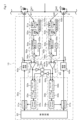
電気的構成を示す図1において、上下アームを構成する2つの半導体スイッチング素子であるNチャンネル型のMOSトランジスタ1、2は、直列接続された状態として電源端子間に接続されている。MOSトランジスタ1および2の共通接続点は負荷への出力端子となっている。また、MOSトランジスタ1はボディダイオード1aを有し、MOSトランジスタ2はボディダイオード2aを有する。
First Embodiment
A first embodiment of the present invention will now be described with reference to FIGS. 1 to 3. FIG.
In Fig. 1 showing the electrical configuration, N-
2個のMOSトランジスタ1、2は、ゲート駆動装置10によりオンオフの駆動制御が行われる。また、2個のMOSトランジスタ1、2には、それぞれ負荷電流であるドレイン電流Id1、Id2をモニタする電流センス機能が備えられている。この場合、電流センス素子を別途設ける構成としても良いし、通電経路に別途電流検出部を設けて検出する構成とすることもできる。
The two
ゲート駆動装置10は、制御回路20、デッドタイム設定回路30a、30b、駆動回路40a、40b、参照電圧調整回路50a、50b、ゲート変動検出回路60を備える。なお、ゲート駆動装置10の構成中、添字a、bを付したデッドタイム設定回路30a、30b、駆動回路40a、40b、参照電圧調整回路50a、50bは、それぞれMOSトランジスタ1、2に対応して個別に設けられたもので、それぞれが同等の内部構成を有している。以下の構成説明では、MOSトランジスタ1に対応する添字aを付した回路について説明し、添字bを付した回路についての説明を省略する。
The
制御回路20は、外部から与えられるオンオフの指示信号に応じて上下アームのMOSトランジスタ1、2に対して駆動信号を作成してオンオフの駆動制御を行う。この場合、制御回路20は、MOSトランジスタ1に対してデッドタイム設定回路30aを介して駆動回路40aに駆動信号を与え、MOSトランジスタ2に対してデッドタイム設定回路30bを介して駆動回路40bに駆動信号を与える。
The
デッドタイム設定回路30aは、検出されたデッドタイムの信号に基づいて指示信号に対して回路構成上で発生する誤差を考慮した所定のマージンを加えてデッドタイムを設定する。デッドタイム設定回路30aは、遅延回路31a、フェーズコンパレータ32a、F/Bゲイン回路33aおよびサンプルアンドホールド回路34aを備えている。
The dead
参照電圧調整回路50aは、MOSトランジスタ1のオンオフのタイミングを判定するための参照電圧Vgsm1を設定してゲート変動検出回路60を構成するコンパレータ61aの反転入力端子に出力する。参照電圧Vgsm1は、MOSトランジスタ1がオンまたはオフ動作中に、ゲート電圧Vgsがミラー期間に入ったときのミラー電圧を示しており、この電圧を超えて変化したときがオンオフのタイミングとなる。
The reference
このため、参照電圧調整回路50aは、次式(1)に基づいてドレイン電流Id1およびしきい値電圧Vthから参照電圧Vgsm1を算出するように回路が構成されている。
For this reason, the reference

なお、式(1)中、ドレイン電流Idはミラー期間中の飽和電流を示しており、そのドレイン電流Idの平方根の前にかかる係数は、MOSトランジスタ1、2のそれぞれのゲート長をL、ゲート幅をW、電子移動度をμn、単位面積あたりのゲート酸化膜容量をCoxとしており、これらは素子によって決まる一定の数値である。また、しきい値電圧Vthについても素子によって決まる一定の数値である。
In equation (1), the drain current Id indicates the saturation current during the mirror period, and the coefficients before the square root of the drain current Id are the gate length L, gate width W, electron mobility μn, and gate oxide film capacitance per unit area Cox of
この結果、しきい値電圧Vthにドレイン電流Idの平方根の値に比例した値を加算した値がミラー電圧Vgsmとなり、これがMOSトランジスタ1、2のオンオフのタイミングを決める参照電圧となる。したがって、負荷電流としてのドレイン電流Idが流れているレベルに応じて参照電圧Vgsmが変化する。
As a result, the mirror voltage Vgsm is calculated by adding a value proportional to the square root of the drain current Id to the threshold voltage Vth, and this becomes the reference voltage that determines the on/off timing of
参照電圧調整回路50aは、電流モニタ部51a、電流方向判定部52a、平方根演算部53a、比例係数乗算部54a、しきい値設定部55a、加算部56aを有する。電流モニタ部51aは、MOSトランジスタ1のドレイン電流Id1の検出信号を取り込み、電流方向判定部52aによりドレイン電流Id1が正の場合すなわちドレイン側からソース側に電流が流れている場合には、ドレイン電流Id1をそのまま出力し、ドレイン電流が負の場合にはゼロとして平方根演算部53aに出力する。
The reference
続いて、平方根演算部53aでドレイン電流Id1の値の平方根の値を演算し、比例係数演算部54aにて比例係数A1を乗じる。加算部56aでは、比例係数演算部54aからの出力と、しきい値設定部55aからのしきい値Vthとを加算して得た参照電圧Vgsm1をゲート変動検出回路60に出力する。
Then, the square root of the drain current Id1 is calculated by the square
ゲート変動検出回路60は、MOSトランジスタ1、2のそれぞれに対応するコンパレータ61a、61bを備えるとともに、それぞれの判定結果を対抗アームに反転して伝えるインバータ62a、62bおよび絶縁通信部63a、63bを備える。
The gate
コンパレータ61aは、MOSトランジスタ1のゲート電圧Vgs1と参照電圧調整回路50aにより設定された参照電圧Vgsm1とを比較し、ゲート電圧Vgs1が参照電圧Vgsm1を超えるとハイレベルの検出信号を出力する。この検出信号は、デッドタイム設定回路30aのフェーズコンパレータ32aに出力されるとともに、インバータ62aおよび絶縁通信部63aを通じて反転した信号がデッドタイム設定回路30bのフェーズコンパレータ32bに出力される。
The
コンパレータ61bについても、同様にして、MOSトランジスタ2のゲート電圧Vgs2と参照電圧調整回路50bにより設定された参照電圧Vgsm2とを比較し、ゲート電圧Vgs2が参照電圧Vgsm2を超えるとハイレベルの検出信号を出力する。この検出信号は、デッドタイム設定回路30bのフェーズコンパレータ32bに出力されるとともに、インバータ62bおよび絶縁通信部63bを通じて反転した信号がデッドタイム設定回路30aのフェーズコンパレータ32aに出力される。
Similarly, the
次に、上記構成の作用について図2および図3も参照して説明する。なお、ゲート駆動装置10の基本的な動作としては、制御回路20からMOSトランジスタ1、2を交互にオンオフ駆動する信号がそれぞれデッドタイム設定回路30a、30bに出力されると、遅延回路31a、31bに設定されているデッドタイムDTに従ったタイミングで駆動信号が生成され、駆動回路40a、40bに出力される。駆動回路40a、40bは、MOSトランジスタ1、2のゲートにゲート駆動信号を与えてオンオフの駆動を行う。
Next, the operation of the above configuration will be described with reference to Figures 2 and 3. The basic operation of the
MOSトランジスタ1、2に流れる負荷電流であるドレイン電流Id1、Id2はそれぞれ計測されており、参照電圧調整回路50a、50bに入力されている。参照電圧調整回路50a、50bにおいては、前述の式(1)に相当する演算処理を実行して参照電圧Vgsm1、Vgsm2を算出し、それぞれコンパレータ61a、61bに設定する。
The drain currents Id1 and Id2, which are the load currents flowing through
この場合、電流方向判定部52a、52bにおいては、ドレイン電流Id1、Id2が正の場合には、その大きさに対応する信号を生成し、負の場合には、電流値はゼロとして生成する。これにより、参照電圧Vgsm1、Vgsm2は、通常の駆動時にはドレイン電流Idに基づいた値が設定され、同期整流時にはしきい値Vth1、Vth2がそれぞれ設定される。
In this case, in the current
前述のように、MOSトランジスタ1、2のオンオフ切り替わり時のゲート電圧Vgs1、Vgs2の大きさは素子がオンオフ動作する過渡期に中間的な電圧が保持されるミラー電圧により決まっている。このため、ミラー電圧は、前述した式(1)に示すように、ドレイン電流Idとしきい値電圧Vthとにより表されている。
As mentioned above, the magnitude of the gate voltages Vgs1 and Vgs2 when
したがって、あらかじめMOSトランジスタ1、2の特性に対応した定数を求めておくことで、参照電圧調整回路50a、50bの比例係数乗算部54aおよびしきい値設定部55aのそれぞれに設定しておけば、ドレイン電流Idに対応したミラー電圧を得ることができる。そして、コンパレータ61a、61bにおいて、ドレイン電流Idに対応して設定したミラー電圧と比較することでオンオフのタイミングを正確に判定することができる。
Therefore, by determining in advance constants corresponding to the characteristics of
また、ドレイン電流Idが負の場合、すなわち同期整流側となっている場合には、オンオフの切り替わりタイミングとなるゲート電圧Vgsは、ドレイン電流Idに依存せず、しきい値電圧Vthとなる。そこで、この場合に対応できるように、参照電圧調整回路50a、50bにおいて、ドレイン電流Idが負となる場合には、電流方向判定部52a、52bが、ドレイン電流Idをゼロとして設定する。これにより、参照電圧はしきい値電圧Vthと等しくなる。
Also, when the drain current Id is negative, i.e., when the synchronous rectification side is selected, the gate voltage Vgs, which is the timing for switching on and off, is the threshold voltage Vth, independent of the drain current Id. Therefore, to accommodate this case, in the reference
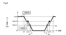
図2はゲート変動検出回路60のコンパレータ61a、61bにてMOSトランジスタ1、2のオンオフタイミングを検出する場合について、負荷電流すなわちドレイン電流Idが大きいレベルと小さいレベルとでゲート電圧Vgsのミラー電圧が異なり、これによって判定タイミングが異なることを示している。
Figure 2 shows that when the
例えばドレイン電流Idが大きいレベルIdHのときに、実線で示すミラー電圧VgsmHとなり、小さいレベルIdLのときに破線で示すミラー電圧VgsmLとなるものとする。コンパレータ61a、61bは、それぞれ、参照電圧Vgsm1、Vgsm2としてドレイン電流Idが大きい場合、小さい場合に応じて、電流値に応じたVgsmH、VgsmLが設定されている。なお、これらの参照電圧Vgsmは、式(1)に基づいて参照電圧調整回路50a、50bにより演算して設定されるものである。
For example, when the drain current Id is at a large level IdH, the mirror voltage VgsmH is shown by the solid line, and when the drain current Id is at a small level IdL, the mirror voltage VgsmL is shown by the dashed line.
MOSトランジスタ1、2がオン状態でゲート電圧Vgsが所定電圧VGSのレベルから時刻t0で下降し始めるとすると、途中のミラー電圧VgsmH、VgsmLで一定レベルとなり、この後、再び下降し始める時刻t1H、t1Lで、コンパレータ61a、61bは参照電圧よりも低下したとして出力信号をハイレベルからローレベルに変化させる。MOSトランジスタ1、2は、それぞれ時刻t1H、t1Lでオフ状態に変化している。
When
したがって、従来相当の参照電圧Vthで判定したタイミングが時刻t1であるとすると、小電流時には時刻t1に比べて若干早いタイミングt1L(図中白丸で示す)で出力信号が変化し、大電流時には時刻t1Lよりもさらに早いタイミングt1H(図中黒丸で示す)で出力が変化する。 Therefore, if the timing determined using the conventional reference voltage Vth is time t1, then when the current is small, the output signal changes at time t1L (shown by a white circle in the figure), which is slightly earlier than time t1, and when the current is large, the output changes at time t1H (shown by a black circle in the figure), which is even earlier than time t1L.
一方、MOSトランジスタ1、2がオフ状態でゲート電圧Vgsがゼロのレベルから時刻t2で上昇し始めるとすると、途中のミラー電圧VgsmL、VgsmHで一定レベルとなり、この後、再び上昇し始める時刻t3H、t3Lで、コンパレータ61a、61bは参照電圧に達したとして出力信号をローレベルからハイレベルに変化させる。MOSトランジスタ1、2は、それぞれ時刻t3L、t3Hでオン状態に変化している。
On the other hand, if the gate voltage Vgs starts to rise from zero level at time t2 while
したがって、従来相当の参照電圧Vthで判定したタイミングが時刻t3であるとすると、小電流時には時刻t3に比べて若干遅いタイミングt3L(図中白丸で示す)で出力信号が変化し、大電流時には時刻t3Lよりもさらに遅いタイミングt3H(図中黒丸で示す)で出力が変化する。 Therefore, if the timing determined using the conventional reference voltage Vth is time t3, then when the current is small, the output signal changes at time t3L (shown by a white circle in the figure), which is slightly later than time t3, and when the current is large, the output changes at time t3H (shown by a black circle in the figure), which is even later than time t3L.
この結果、ドレイン電流Idの大小に応じてオンオフのタイミングがずれるとともに、ドレイン電流Idが大きいほど、しきい値電圧Vthでの検出タイミングからの時間差が長くなっていることがわかる。 As a result, it can be seen that the on/off timing differs depending on the magnitude of the drain current Id, and the larger the drain current Id, the longer the time difference from the detection timing at the threshold voltage Vth.
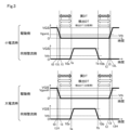
図3は、上記したゲート変動検出回路60のコンパレータ61a、61bにてMOSトランジスタ1、2のオンオフタイミングを検出する動作に基づいて、上下アームのMOSトランジスタ1、2が、一方が駆動側(上段に表示)、他方が同期整流側(下段に表示)となる場合のオンオフの動作について、ドレイン電流Idが大電流時と小電流時とで示している。
Figure 3 shows the on/off operation of the upper and lower
前述したように、小電流時は、参照電圧Vgsmが低いレベルであるVgsmLとなり、しきい値電圧Vthよりも少し大きい値となっている。また、大電流時には高いレベルであるVgsmHとなっている。 As mentioned above, when the current is small, the reference voltage Vgsm is at a low level, VgsmL, which is slightly larger than the threshold voltage Vth. When the current is large, the reference voltage Vgsm is at a high level, VgsmH.
まず、ドレイン電流Idが小電流時には、MOSトランジスタ1、2のうちの駆動側のものが時刻t0でオフ駆動されると、ゲート電圧Vgsが印加されていたVGSから下降していく。時刻t1Lで参照電圧VgsmLに達し、オフ状態に移行する。そして、この後時刻t1でしきい値電圧Vthに達する。
First, when the drain current Id is small, the driving one of the
ここで、デッドタイムDTの開始時点は、オフ状態に移行した時刻t1Lであり、実デッドタイムと検出デッドタイムDTの開始時刻はほぼ同じである。一方、しきい値電圧Vthで判定する従来方式の比較例では、少し遅れてオフタイミングが検出される。 Here, the start point of the dead time DT is the time t1L when the switch transitions to the off state, and the start times of the actual dead time and the detected dead time DT are almost the same. On the other hand, in a comparative example of the conventional method that uses the threshold voltage Vth for determination, the off timing is detected with a slight delay.
この後、デッドタイムDTが経過してMOSトランジスタ1、2のうちの同期整流側のものが時刻T0aでオン駆動されると、ゲート電圧Vgsが上昇し、時刻Taでしきい値電圧Vthに達してオン状態となり、この時刻Taが検出される。
After this, when the dead time DT has elapsed and the synchronous rectification side of the
これにより、このときの実デッドタイムは時刻t1Lから時刻Taまでとなり、検出デッドタイムDTとほぼ同じである。これに対して、比較例では、駆動側のオフ時刻がt1Lよりも遅れた時刻t1で検出されることで、少し短い検出デッドタイムとなるため、実デッドタイムとの差が発生している。 As a result, the actual dead time at this time is from time t1L to time Ta, which is approximately the same as the detected dead time DT. In contrast, in the comparative example, the drive side off time is detected at time t1, which is later than t1L, resulting in a slightly shorter detected dead time, which results in a difference from the actual dead time.
次に、ドレイン電流Idが大電流時には、MOSトランジスタ1、2のうちの駆動側のものが時刻t0でオフ駆動されると、ゲート電圧Vgsが印加されていたVGSから下降し始めて、時刻t1Hで参照電圧VgsmHに達し、オフ状態に移行する。そして、この後時刻t1でしきい値電圧Vthに達する。
Next, when the drain current Id is large, the driving one of the
ここでのデッドタイムDTの開始時点は、オフ状態に移行した時刻t1Hであり、実デッドタイムと検出デッドタイムDTの開始時刻はほぼ同じである。一方、しきい値電圧Vthで判定する従来方式の比較例では、遅れてオフタイミングが検出される。 The start time of the dead time DT here is the time t1H when the device transitions to the off state, and the start times of the actual dead time and the detected dead time DT are almost the same. On the other hand, in a comparative example of the conventional method that uses the threshold voltage Vth for determination, the off timing is detected with a delay.
この後、デッドタイムDTが経過してMOSトランジスタ1、2のうちの同期整流側のものが時刻T0aでオン駆動されると、ゲート電圧Vgsが上昇し、時刻Taでしきい値電圧Vthに達してオン状態となり、この時刻Taが検出される。
After this, when the dead time DT has elapsed and the synchronous rectification side of the
これにより、このときの実デッドタイムは時刻t1Hから時刻Taまでとなり、この場合においても検出デッドタイムDTとほぼ同じである。これに対して、比較例では、駆動側のオフ時刻がt1Hよりも遅れた時刻t1で検出されることで、少し短い検出デッドタイムとなるため、実デッドタイムとの差が大きく発生している。 As a result, the actual dead time at this time is from time t1H to time Ta, which is also approximately the same as the detected dead time DT. In contrast, in the comparative example, the drive side off time is detected at time t1, which is later than t1H, resulting in a slightly shorter detected dead time, and a large difference from the actual dead time occurs.
上記の検出誤差は、ドレイン電流Idが大きくなるほど大きくなる。このため、従来においては、このような検出誤差を考慮したマージンを加算してデッドタイムを設定していた。このため、ドレイン電流Idが小さい場合でも必要以上にデッドタイムが大きく設定されることとなっていた。 The above detection error increases as the drain current Id increases. For this reason, in the past, the dead time was set by adding a margin that took such detection errors into account. As a result, even when the drain current Id was small, the dead time was set longer than necessary.
このような本実施形態においては、参照電圧調整回路50a、50bにより、MOSトランジスタ1、2のオンオフのタイミングを負荷電流であるドレイン電流Id1、Id2の大きさに応じて参照電圧Vgsm1、Vgsm2として設定するようにした。これにより、ドレイン電流Id1、Id2が変動しても、実際にMOSトランジスタ1、2がオンオフするタイミングと、ゲート電圧Vgsの変動を検出するタイミングが一致させることができ、検出デッドタイムと実デッドタイムの長さを一致させることができる。
In this embodiment, the reference
この結果、ドレイン電流Id1、Id2の大きさに起因して変動する検出デッドタイムDTの変動分含めた状態で検出することができるようになり、このような変動分を考慮してデッドタイムにマージンを設定する必要が無くなり、その分、設定するデッドタイムの短縮を図ることができる。 As a result, it is possible to detect the detection dead time DT including the fluctuation caused by the magnitude of the drain currents Id1 and Id2, eliminating the need to set a margin in the dead time to take such fluctuations into account, and therefore making it possible to shorten the dead time to be set.
(第2実施形態)
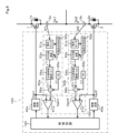
図4は第2実施形態を示すもので、以下、第1実施形態と異なる部分について説明する。この実施形態では、ゲート駆動装置100は、デッドタイム設定回路30a、30bの機能を制御回路120において実行する構成とされ、また、これによって、ゲート変動検出回路160はコンパレータ61a、61bを設ける構成としている。
Second Embodiment
4 shows the second embodiment, and the following describes the differences from the first embodiment. In this embodiment, the
また、この実施形態においては、MOSトランジスタ1、2の電流検出機能を用いるのではなく、それぞれの通電経路にドレイン電流Id1、Id2を検出するように、電流検出センサ3a、3bを設ける構成としている。参照電圧調整回路50a、50bの電流モニタ部51a、51bは、それぞれの電流検出センサ3a、3bから電流検出信号が入力されるように構成されている。
In addition, in this embodiment, instead of using the current detection function of
制御回路120は、ゲート変動検出回路160から出力されるMOSトランジスタ1、2のゲート電圧の変動の検出信号により実デッドタイムを算出し、マージンを加えてデッドタイムを設定した値に基づいて、駆動回路40a、40bに駆動信号を与える構成である。
したがって、このような第3実施形態においても第1実施形態と同様の作用効果を得ることができる。
The
Therefore, in the third embodiment as described above, the same effects as those in the first embodiment can be obtained.
(第3実施形態)
図5および図6は第3実施形態を示すもので、以下、第1実施形態と異なる部分について説明する。この実施形態では、ゲート駆動装置110は、参照電圧調整回路150a、150bとして、それぞれのMOSトランジスタ1、2の温度をモニタする機能を備えた構成としている。温度モニタの構成としては、例えば、検出部位にダイオードを配置し、これに一定電流を流す構成が設けられる。ダイオードに一定電流が流れたときの順方向電圧を検出することで温度を算出することができる。
Third Embodiment
5 and 6 show the third embodiment, and the following describes the differences from the first embodiment. In this embodiment, the
以下、参照電圧調整回路150a、150bは、同等の構成となっており、以下の説明では参照電圧調整回路150aについて説明する。温度モニタ部57aは、MOSトランジスタ1からの温度に対応した信号が入力されると、温度信号をしきい値設定部55aに出力する。しきい値設定部55aは、温度Tに対応したしきい値Vthの値を加算器56aに出力する。
The reference
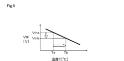
第1実施形態においては、前述した式(1)に示したしきい値電圧Vthの値は、MOSトランジスタ1、2のそれぞれの固有の値として扱っていたが、実際には使用環境温度やドレイン電流Idが流れることにより素子温度が変化すると、これに応じてしきい値電圧Vthについての変化する特性を有している。
In the first embodiment, the value of the threshold voltage Vth shown in the above-mentioned formula (1) was treated as a value specific to each of the
このしきい値電圧Vthの温度特性は、図6に示すように、温度Tが上昇するとこれに応じて例えば図示のように直線的に減少する関係にある。図6に示しているように、温度TがTaからTbに上昇すると、しきい値電圧Vthは、VthaからVthbに低下する。 As shown in FIG. 6, the temperature characteristic of this threshold voltage Vth is such that as the temperature T increases, the threshold voltage Vth decreases linearly, for example, as shown in the figure. As shown in FIG. 6, when the temperature T increases from Ta to Tb, the threshold voltage Vth decreases from Vtha to Vthb.
温度モニタ部57a、57bは、MOSトランジスタ1、2の温度Tの検出信号を入力して検出温度に対応した信号をしきい値設定部55a、55bに出力する。しきい値設定部55aは、あらかじめMOSトランジスタ1の温度特性に対応するデータが記憶されており、温度信号Tが入力されると、これに対応したしきい値Vth(T)を読み出して出力する。なお、図6に示す温度としきい値電圧との関係を数式として記憶し、算出して出力するようにしても良い。
The
これにより、参照電圧調整回路150aは、MOSトランジスタ1のドレイン電流Id1の大きさと温度Tとに応じて参照電圧Vgsm1をコンパレータ61aに設定することができる。
This allows the reference
この結果、MOSトランジスタ1、2がオンオフするタイミングをより正確に検出することができ、マージンの設定を回路中の誤差に起因するわずかな分だけ設定することができ、デッドタイムの検出を精度良く行うことができる。特に、同期整流時には、参照電圧としてしきい値電圧Vthが温度に対応して設定されるので、オンオフのタイミングを正確に検出することができるようになる。
As a result, the on/off timing of
このような本実施形態によれば、MOSトランジスタ1、2のドレイン電流Id1、Id2の大きさだけでなく、素子温度T1、T2にも対応して、オンオフのタイミングを検出するための参照電圧Vgsm1、Vgsm2を設定することができるようになる。
According to this embodiment, it is possible to set the reference voltages Vgsm1 and Vgsm2 for detecting the on/off timing in response not only to the magnitude of the drain currents Id1 and Id2 of the
なお、装置の使用環境や使用形態によっては、温度変化が少なくしきい値電圧Vthの変動も少ない場合には、一定値として設定する第1実施形態の構成を用いることでも支障はない。そして、この実施形態で扱うように、素子温度の変動に伴うしきい値電圧Vthの変化が大きくなる場合には、本実施形態を適用することでデッドタイムを精度良く検出することができる。 Depending on the environment and usage of the device, if there is little temperature change and little fluctuation in the threshold voltage Vth, there is no problem in using the configuration of the first embodiment in which the threshold voltage Vth is set to a constant value. And, in cases where the change in the threshold voltage Vth due to fluctuations in the element temperature becomes large, as in this embodiment, the dead time can be detected with high accuracy by applying this embodiment.
(他の実施形態)
なお、本発明は、上述した実施形態のみに限定されるものではなく、その要旨を逸脱しない範囲で種々の実施形態に適用可能であり、例えば、以下のように変形または拡張することができる。
Other Embodiments
The present invention is not limited to the above-described embodiment, but can be applied to various embodiments without departing from the spirit of the present invention, and can be modified or expanded as follows, for example.
半導体スイッチング素子として、MOSトランジスタは、一般的なシリコン(Si)製のもの以外に、炭化シリコン(SiC)のものを用いることもできるし、また、IGBT(Insulated Gate Bipolar Transistor)などのゲート駆動型のスイッチング素子に適用することができる。 As semiconductor switching elements, MOS transistors can be used that are made of silicon carbide (SiC) in addition to the typical silicon (Si) transistors, and can also be applied to gate-driven switching elements such as IGBTs (Insulated Gate Bipolar Transistors).
本開示は、実施例に準拠して記述されたが、本開示は当該実施例や構造に限定されるものではないと理解される。本開示は、様々な変形例や均等範囲内の変形をも包含する。加えて、様々な組み合わせや形態、さらには、それらに一要素のみ、それ以上、あるいはそれ以下、を含む他の組み合わせや形態をも、本開示の範疇や思想範囲に入るものである。 Although the present disclosure has been described with reference to the embodiment, it is understood that the present disclosure is not limited to the embodiment or structure. The present disclosure also encompasses various modifications and modifications within the scope of equivalents. In addition, various combinations and forms, as well as other combinations and forms including only one element, more than one element, or less than one element, are also within the scope and concept of the present disclosure.
図面中、1、2はMOSトランジスタ(ゲート駆動型の半導体スイッチング素子)、3a、3bは電流検出素子、10、100、110はゲート駆動装置、20は制御回路、30a、30bはデッドタイム設定回路、40a、40bは駆動回路、50a、50bは参照電圧調整回路、60はゲート変動検出回路、61a、61bはコンパレータである。 In the drawing, 1 and 2 are MOS transistors (gate-driven semiconductor switching elements), 3a and 3b are current detection elements, 10, 100, and 110 are gate drive devices, 20 is a control circuit, 30a and 30b are dead time setting circuits, 40a and 40b are drive circuits, 50a and 50b are reference voltage adjustment circuits, 60 is a gate fluctuation detection circuit, and 61a and 61b are comparators.
Claims (5)
前記上下アームのそれぞれの半導体スイッチング素子を交互に駆動するための駆動信号を送信する制御回路(20)と、
前記制御回路からの駆動信号に応じて前記上下アームのそれぞれの半導体スイッチング素子のゲートを駆動する駆動回路(40a、40b)と、
前記上下アームのそれぞれの半導体スイッチング素子についてゲート電圧が参照電圧と一致するタイミングを検出するゲート変動検出回路(60)と、
前記半導体スイッチング素子の電流値に応じて前記ゲート変動検出回路の前記参照電圧を調整する参照電圧調整回路(50a、50b)とを備え、
前記制御回路は、前記ゲート変動検出回路により検出される前記上下アームの前記半導体スイッチング素子のゲート電圧変動のタイミングからデッドタイムを算出し、次に駆動する側の駆動タイミングを調整するタイミング調整機能を備えるゲート駆動装置。 A gate drive device for driving gates of gate-driven semiconductor switching elements each having a rectifier element disposed on an upper arm and a lower arm, comprising:
A control circuit (20) that transmits drive signals for alternately driving the semiconductor switching elements of the upper and lower arms;
a drive circuit (40a, 40b) for driving gates of the semiconductor switching elements of the upper and lower arms in response to a drive signal from the control circuit;
a gate fluctuation detection circuit (60) for detecting a timing at which a gate voltage of each of the upper and lower arm semiconductor switching elements coincides with a reference voltage;
a reference voltage adjustment circuit (50a, 50b) that adjusts the reference voltage of the gate fluctuation detection circuit in accordance with a current value of the semiconductor switching element;
The control circuit is a gate drive device having a timing adjustment function that calculates a dead time from the timing of the gate voltage fluctuation of the semiconductor switching elements of the upper and lower arms detected by the gate fluctuation detection circuit, and adjusts the drive timing of the side to be driven next.
Priority Applications (1)
| Application Number | Priority Date | Filing Date | Title |
|---|---|---|---|
| JP2021041380A JP7561663B2 (en) | 2021-03-15 | 2021-03-15 | Gate Driver |
Applications Claiming Priority (1)
| Application Number | Priority Date | Filing Date | Title |
|---|---|---|---|
| JP2021041380A JP7561663B2 (en) | 2021-03-15 | 2021-03-15 | Gate Driver |
Publications (2)
| Publication Number | Publication Date |
|---|---|
| JP2022141181A JP2022141181A (en) | 2022-09-29 |
| JP7561663B2 true JP7561663B2 (en) | 2024-10-04 |
Family
ID=83403173
Family Applications (1)
| Application Number | Title | Priority Date | Filing Date |
|---|---|---|---|
| JP2021041380A Active JP7561663B2 (en) | 2021-03-15 | 2021-03-15 | Gate Driver |
Country Status (1)
| Country | Link |
|---|---|
| JP (1) | JP7561663B2 (en) |
Citations (3)
| Publication number | Priority date | Publication date | Assignee | Title |
|---|---|---|---|---|
| JP2002272131A (en) | 2001-03-07 | 2002-09-20 | Fuji Electric Co Ltd | Gate drive circuit for power semiconductor device |
| JP2010016937A (en) | 2008-07-02 | 2010-01-21 | Yaskawa Electric Corp | Power conversion device and dead time compensation method |
| JP2015216818A (en) | 2014-05-13 | 2015-12-03 | 株式会社デンソー | Switching element drive circuit |
-
2021
- 2021-03-15 JP JP2021041380A patent/JP7561663B2/en active Active
Patent Citations (3)
| Publication number | Priority date | Publication date | Assignee | Title |
|---|---|---|---|---|
| JP2002272131A (en) | 2001-03-07 | 2002-09-20 | Fuji Electric Co Ltd | Gate drive circuit for power semiconductor device |
| JP2010016937A (en) | 2008-07-02 | 2010-01-21 | Yaskawa Electric Corp | Power conversion device and dead time compensation method |
| JP2015216818A (en) | 2014-05-13 | 2015-12-03 | 株式会社デンソー | Switching element drive circuit |
Also Published As
| Publication number | Publication date |
|---|---|
| JP2022141181A (en) | 2022-09-29 |
Similar Documents
| Publication | Publication Date | Title |
|---|---|---|
| US9829387B2 (en) | System and method for temperature sensing | |
| US11025243B2 (en) | Power circuit | |
| JP5862434B2 (en) | Power transistor drive circuit | |
| US7969227B2 (en) | Temperature detection circuit | |
| US6838914B2 (en) | Semiconductor device | |
| US9929073B2 (en) | Semiconductor device | |
| CN112823469A (en) | Gate driving device | |
| JP6286899B2 (en) | Insulated gate type semiconductor device driving apparatus and power conversion apparatus | |
| US10050031B2 (en) | Power conventer and semiconductor device | |
| US20240291402A1 (en) | Semiconductor device and power conversion device | |
| US10256807B2 (en) | Driving device for semiconductor elements | |
| CN115211009B (en) | Gate drive device | |
| CN111512528B (en) | Power conversion device | |
| US10715136B2 (en) | Current sense devices and associated methods | |
| US11211924B2 (en) | Electronic circuit | |
| CN111880068A (en) | Circuit arrangement and method for controlling a power semiconductor switch | |
| WO1997033370A1 (en) | Temperature-compensated driver circuit | |
| JP7041887B2 (en) | Load drive | |
| JP7561663B2 (en) | Gate Driver | |
| US20240146179A1 (en) | Driving device for semiconductor element, and power conversion device | |
| WO2018096828A1 (en) | Gate drive device | |
| RU2754501C1 (en) | Control of metal-oxide-semiconductor field-effect transistor | |
| CN117728653A (en) | Electronic circuits, power conversion devices and inverters | |
| CN116893015A (en) | Semiconductor device |
Legal Events
| Date | Code | Title | Description |
|---|---|---|---|
| A621 | Written request for application examination |
Free format text: JAPANESE INTERMEDIATE CODE: A621 Effective date: 20231211 |
|
| A977 | Report on retrieval |
Free format text: JAPANESE INTERMEDIATE CODE: A971007 Effective date: 20240820 |
|
| TRDD | Decision of grant or rejection written | ||
| A01 | Written decision to grant a patent or to grant a registration (utility model) |
Free format text: JAPANESE INTERMEDIATE CODE: A01 Effective date: 20240827 |
|
| A61 | First payment of annual fees (during grant procedure) |
Free format text: JAPANESE INTERMEDIATE CODE: A61 Effective date: 20240924 |
|
| R150 | Certificate of patent or registration of utility model |
Ref document number: 7561663 Country of ref document: JP Free format text: JAPANESE INTERMEDIATE CODE: R150 |