JP7561579B2 - Etching method and etching apparatus - Google Patents
Etching method and etching apparatus Download PDFInfo
- Publication number
- JP7561579B2 JP7561579B2 JP2020188278A JP2020188278A JP7561579B2 JP 7561579 B2 JP7561579 B2 JP 7561579B2 JP 2020188278 A JP2020188278 A JP 2020188278A JP 2020188278 A JP2020188278 A JP 2020188278A JP 7561579 B2 JP7561579 B2 JP 7561579B2
- Authority
- JP
- Japan
- Prior art keywords
- film
- etching
- silicon oxide
- gas
- chamber
- Prior art date
- Legal status (The legal status is an assumption and is not a legal conclusion. Google has not performed a legal analysis and makes no representation as to the accuracy of the status listed.)
- Active
Links
Images


Classifications
-
- H—ELECTRICITY
- H10—SEMICONDUCTOR DEVICES; ELECTRIC SOLID-STATE DEVICES NOT OTHERWISE PROVIDED FOR
- H10P—GENERIC PROCESSES OR APPARATUS FOR THE MANUFACTURE OR TREATMENT OF DEVICES COVERED BY CLASS H10
- H10P50/00—Etching of wafers, substrates or parts of devices
- H10P50/20—Dry etching; Plasma etching; Reactive-ion etching
- H10P50/28—Dry etching; Plasma etching; Reactive-ion etching of insulating materials
- H10P50/282—Dry etching; Plasma etching; Reactive-ion etching of insulating materials of inorganic materials
- H10P50/283—Dry etching; Plasma etching; Reactive-ion etching of insulating materials of inorganic materials by chemical means
-
- H—ELECTRICITY
- H10—SEMICONDUCTOR DEVICES; ELECTRIC SOLID-STATE DEVICES NOT OTHERWISE PROVIDED FOR
- H10P—GENERIC PROCESSES OR APPARATUS FOR THE MANUFACTURE OR TREATMENT OF DEVICES COVERED BY CLASS H10
- H10P14/00—Formation of materials, e.g. in the shape of layers or pillars
- H10P14/60—Formation of materials, e.g. in the shape of layers or pillars of insulating materials
- H10P14/63—Formation of materials, e.g. in the shape of layers or pillars of insulating materials characterised by the formation processes
- H10P14/6326—Deposition processes
- H10P14/6328—Deposition from the gas or vapour phase
- H10P14/6334—Deposition from the gas or vapour phase using decomposition or reaction of gaseous or vapour phase compounds, i.e. chemical vapour deposition
- H10P14/6339—Deposition from the gas or vapour phase using decomposition or reaction of gaseous or vapour phase compounds, i.e. chemical vapour deposition deposition by cyclic CVD, e.g. ALD, ALE or pulsed CVD
-
- H—ELECTRICITY
- H10—SEMICONDUCTOR DEVICES; ELECTRIC SOLID-STATE DEVICES NOT OTHERWISE PROVIDED FOR
- H10P—GENERIC PROCESSES OR APPARATUS FOR THE MANUFACTURE OR TREATMENT OF DEVICES COVERED BY CLASS H10
- H10P14/00—Formation of materials, e.g. in the shape of layers or pillars
- H10P14/60—Formation of materials, e.g. in the shape of layers or pillars of insulating materials
- H10P14/66—Formation of materials, e.g. in the shape of layers or pillars of insulating materials characterised by the type of materials
- H10P14/662—Laminate layers, e.g. stacks of alternating high-k metal oxides
-
- H—ELECTRICITY
- H10—SEMICONDUCTOR DEVICES; ELECTRIC SOLID-STATE DEVICES NOT OTHERWISE PROVIDED FOR
- H10P—GENERIC PROCESSES OR APPARATUS FOR THE MANUFACTURE OR TREATMENT OF DEVICES COVERED BY CLASS H10
- H10P14/00—Formation of materials, e.g. in the shape of layers or pillars
- H10P14/60—Formation of materials, e.g. in the shape of layers or pillars of insulating materials
- H10P14/69—Inorganic materials
- H10P14/692—Inorganic materials composed of oxides, glassy oxides or oxide-based glasses
- H10P14/6921—Inorganic materials composed of oxides, glassy oxides or oxide-based glasses containing silicon
- H10P14/69215—Inorganic materials composed of oxides, glassy oxides or oxide-based glasses containing silicon the material being a silicon oxide, e.g. SiO2
-
- H—ELECTRICITY
- H10—SEMICONDUCTOR DEVICES; ELECTRIC SOLID-STATE DEVICES NOT OTHERWISE PROVIDED FOR
- H10P—GENERIC PROCESSES OR APPARATUS FOR THE MANUFACTURE OR TREATMENT OF DEVICES COVERED BY CLASS H10
- H10P14/00—Formation of materials, e.g. in the shape of layers or pillars
- H10P14/60—Formation of materials, e.g. in the shape of layers or pillars of insulating materials
- H10P14/69—Inorganic materials
- H10P14/692—Inorganic materials composed of oxides, glassy oxides or oxide-based glasses
- H10P14/6921—Inorganic materials composed of oxides, glassy oxides or oxide-based glasses containing silicon
- H10P14/6922—Inorganic materials composed of oxides, glassy oxides or oxide-based glasses containing silicon the material containing Si, O and at least one of H, N, C, F or other non-metal elements, e.g. SiOC, SiOC:H or SiONC
- H10P14/6927—Inorganic materials composed of oxides, glassy oxides or oxide-based glasses containing silicon the material containing Si, O and at least one of H, N, C, F or other non-metal elements, e.g. SiOC, SiOC:H or SiONC the material being a silicon oxynitride, e.g. SiON or SiON:H
-
- H—ELECTRICITY
- H10—SEMICONDUCTOR DEVICES; ELECTRIC SOLID-STATE DEVICES NOT OTHERWISE PROVIDED FOR
- H10P—GENERIC PROCESSES OR APPARATUS FOR THE MANUFACTURE OR TREATMENT OF DEVICES COVERED BY CLASS H10
- H10P14/00—Formation of materials, e.g. in the shape of layers or pillars
- H10P14/60—Formation of materials, e.g. in the shape of layers or pillars of insulating materials
- H10P14/69—Inorganic materials
- H10P14/694—Inorganic materials composed of nitrides
- H10P14/6943—Inorganic materials composed of nitrides containing silicon
- H10P14/69433—Inorganic materials composed of nitrides containing silicon the material being a silicon nitride not containing oxygen, e.g. SixNy or SixByNz
-
- H—ELECTRICITY
- H10—SEMICONDUCTOR DEVICES; ELECTRIC SOLID-STATE DEVICES NOT OTHERWISE PROVIDED FOR
- H10P—GENERIC PROCESSES OR APPARATUS FOR THE MANUFACTURE OR TREATMENT OF DEVICES COVERED BY CLASS H10
- H10P70/00—Cleaning of wafers, substrates or parts of devices
- H10P70/20—Cleaning during device manufacture
- H10P70/23—Cleaning during device manufacture during, before or after processing of insulating materials
-
- H—ELECTRICITY
- H10—SEMICONDUCTOR DEVICES; ELECTRIC SOLID-STATE DEVICES NOT OTHERWISE PROVIDED FOR
- H10P—GENERIC PROCESSES OR APPARATUS FOR THE MANUFACTURE OR TREATMENT OF DEVICES COVERED BY CLASS H10
- H10P72/00—Handling or holding of wafers, substrates or devices during manufacture or treatment thereof
- H10P72/04—Apparatus for manufacture or treatment
- H10P72/0402—Apparatus for fluid treatment
- H10P72/0418—Apparatus for fluid treatment for etching
- H10P72/0421—Apparatus for fluid treatment for etching for drying etching
Landscapes
- Drying Of Semiconductors (AREA)
Description
本開示は、エッチング方法およびエッチング装置に関する。 This disclosure relates to an etching method and an etching apparatus.
近時、半導体デバイスの製造過程で、チャンバー内でプラズマを生成することなく化学的にエッチングを行う化学的酸化物除去処理(Chemical Oxide Removal;COR)と呼ばれる手法が知られている。CORとしては、基板である半導体ウエハの表面に存在するシリコン酸化膜(SiO2膜)に、フッ素含有ガスであるフッ化水素(HF)ガスと塩基性ガスであるアンモニア(NH3)ガスを用いる技術が知られている(例えば特許文献1、2)。この技術では、HFガスとNH3ガスをシリコン酸化膜と反応させてケイフッ化アンモニウム((NH4)2SiF6;AFS)を生成させ、加熱によりこのケイフッ化アンモニウムを昇華させることにより、シリコン酸化膜がエッチングされる。
Recently, a method called Chemical Oxide Removal (COR) is known in which etching is performed chemically without generating plasma in a chamber during the manufacturing process of semiconductor devices. As a COR method, a technique is known in which hydrogen fluoride (HF) gas, which is a fluorine-containing gas, and ammonia (NH 3 ) gas, which is a basic gas, are used on a silicon oxide film (SiO 2 film) present on the surface of a semiconductor wafer, which is a substrate (see, for example,
本開示は、第1の酸化シリコン系膜と窒化シリコン系膜と第2の酸化シリコン系膜の3層積層膜を一括して除去することができるエッチング方法およびエッチング装置を提供する。 This disclosure provides an etching method and an etching apparatus that can simultaneously remove a three-layer stacked film consisting of a first silicon oxide film, a silicon nitride film, and a second silicon oxide film.
本開示の一態様に係るエッチング方法は、第1の酸化シリコン系膜と窒化シリコン系膜と第2の酸化シリコン系膜とを積層してなる3層積層膜を有する基板をチャンバー内に設ける工程と、前記チャンバー内で、HF-NH3系ガスを用い、前記3層積層膜を、各膜におけるガス比を調整しつつ一括してエッチングする工程と、を有する。 An etching method according to one aspect of the present disclosure includes the steps of: providing a substrate having a three-layer laminated film formed by laminating a first silicon oxide-based film, a silicon nitride-based film, and a second silicon oxide-based film in a chamber; and using an HF-NH3 - based gas in the chamber to etch the three-layer laminated film all at once while adjusting the gas ratio for each film.
本開示によれば、第1の酸化シリコン系膜と窒化シリコン系膜と第2の酸化シリコン系膜の3層積層膜を一括して除去することができるエッチング方法およびエッチング装置が提供される。 The present disclosure provides an etching method and an etching apparatus that can simultaneously remove a three-layer stacked film of a first silicon oxide film, a silicon nitride film, and a second silicon oxide film.
以下、図面を参照しながら、実施形態について説明する。 The following describes the embodiment with reference to the drawings.
<エッチング装置>
図1は、一実施形態のエッチング方法の実施に用いられるエッチング装置の一例を示す断面図である。
<Etching equipment>
FIG. 1 is a cross-sectional view showing an example of an etching apparatus used to carry out an etching method according to an embodiment of the present invention.
図1に示すように、エッチング装置1は、密閉構造のチャンバー10を備えており、チャンバー10の内部には、基板Wを略水平にした状態で載置させる載置台12が設けられている。
As shown in FIG. 1, the
また、エッチング装置1は、チャンバー10に処理ガスを供給するガス供給機構13、チャンバー10内を排気する排気機構14を備えている。
The
チャンバー10は、チャンバー本体21と蓋部22とによって構成されている。チャンバー本体21は、略円筒形状の側壁部21aと底部21bとを有し、上部は開口となっており、この開口が内部に凹部を有する蓋部22で閉止される。側壁部21aと蓋部22とは、シール部材(図示せず)により密閉されて、チャンバー10内の気密性が確保される。
The
蓋部22の内部には、載置台12に臨むようにガス導入部材であるシャワーヘッド26がはめ込まれている。シャワーヘッド26は円筒状をなす本体31と、本体31の底部に設けられたシャワープレート32とを有している。本体31とシャワープレート32とで形成される空間には、シャワープレート32と平行に中間プレート33が設けられており、本体31の上部壁31aと中間プレート33との間は第1の空間34aとなっており、中間プレート33とシャワープレート32との間は第2の空間34bとなっている。
A
第1の空間34aには、ガス供給機構13の第1のガス供給配管61が挿入されており、第1の空間34aに繋がる複数のガス通路35が中間プレート33から第2空間34bに設けられたスペーサ36を通ってシャワープレート32の上面まで延びている。このガス通路35は、シャワープレート32に形成された複数の第1のガス吐出孔37に繋がっている。一方、第2の空間34bには、ガス供給機構の第2のガス供給配管63が挿入されており、この第2の空間34bには、シャワープレート32に形成された複数の第2のガス吐出孔38が繋がっている。
A first
そして、第1のガス供給配管61から第1の空間34aに供給されたガスがガス通路35および第1のガス吐出孔37を経てチャンバー10内へ吐出される。また、第2のガス供給配管63から第2の空間34bに供給されたガスが第2のガス吐出孔38から吐出される。すなわち、第1のガス供給配管61から供給されたガスと、第2のガス供給配管63から供給されたガスがシャワーヘッド26から吐出した後に混合されるポストミックスタイプとなっている。
The gas supplied from the first
なお、第1のガス供給配管61から供給されたガスと、第2のガス供給配管63から供給されたガスがシャワーヘッド内で混合されるプレミックスタイプであってもよい。
In addition, the shower head may be of a premix type in which the gas supplied from the first
チャンバー本体21の側壁部21aには、基板Wを搬入出する搬入出口41が設けられており、この搬入出口41はゲートバルブ42により開閉可能となっており、隣接する他のモジュールとの間で基板Wが搬送可能となっている。
A loading/
載置台12は、平面視略円形をなしており、チャンバー10の底部21bに固定されている。載置台12の内部には、載置台12の温度を調節する温調器45が設けられている。温調器45は、例えば、温度を調節する温調媒体(例えば水など)が循環する温調媒体流路や、抵抗ヒーターで構成することができる。温調器45により載置台12が所望の温度に温調され、これにより載置台12に載置された基板Wの温度制御がなされる。
The mounting table 12 is generally circular in plan view and is fixed to the
ガス供給機構13は、HFガス供給源51、Arガス供給源52、NH3ガス供給源53、およびN2ガス供給源54を有している。
The
HFガス供給源51はHFガスを供給するものであり、NH3ガス供給源53はNH3ガスを供給するものである。Arガス供給源52およびN2ガス供給源54は、希釈ガス、パージガス、キャリアガスとしての機能を兼ね備えた不活性ガスとして、N2ガス、Arガスを供給するものである。ただし、両方ともArガスまたはN2ガスであってもよい。また、不活性ガスはArガスおよびN2ガスに限定されず、Heガス等の他の希ガスを用いることもできる。
The HF
これらガス供給源51~54には、それぞれ第1~第4のガス供給配管61~64の一端が接続されている。HFガス供給源51に接続された第1のガス供給配管61は、上述したようにその他端がシャワーヘッド26の第1の空間34aに挿入されている。Arガス供給源52に接続された第2のガス供給配管62は、その他端が第1のガス供給配管61に接続されている。NH3ガス供給源53に接続された第3のガス供給配管63は、上述したようにその他端がシャワーヘッド26の第2の空間34bに挿入されている。N2ガス供給源54に接続された第4のガス供給配管64は、その他端が第3のガス供給配管63に接続されている。
These
HFガスとNH3ガスは、それぞれ不活性ガスであるArガスおよびN2ガスとともに、それぞれシャワーヘッド26の第1の空間34aおよび第2の空間34bに至り、ガス吐出孔37およびガス吐出孔38からチャンバー10内に吐出される。
The HF gas and NH3 gas, together with the inert gases Ar gas and N2 gas, reach the
第1~第4のガス供給配管61~64には、流路の開閉動作および流量制御を行う流量制御部65が設けられている。流量制御部65は例えば開閉弁およびマスフローコントローラ(MFC)またはフローコントロールシステム(FCS)のような流量制御器により構成されている。
The first to fourth
排気機構14は、チャンバー10の底部21bに形成された排気口71に繋がる排気配管72を有しており、さらに、排気配管72に設けられた、チャンバー10内の圧力を制御するための自動圧力制御弁(APC)73およびチャンバー10内を排気するための真空ポンプ74を有している。
The
チャンバー10の側壁には、チャンバー10内の圧力制御のために高圧用および低圧用の2つのキャパシタンスマノメータ76a,76bが設けられている。載置台12に載置された基板Wの近傍には、基板Wの温度を検出する温度センサ(図示せず)が設けられている。
Two
エッチング装置1を構成するチャンバー10、シャワーヘッド26、載置台12は、アルミニウムのような金属材料で形成されている。これらの表面には酸化皮膜等の皮膜が形成されていてもよい。
The
エッチング装置1は、さらに制御部80を有している。制御部80はコンピュ
ータで構成されており、CPUを備えた主制御部と、入力装置、出力装置、表示装置、記憶装置(記憶媒体)を有している。主制御部は、エッチング装置1の各構成部の動作を制御する。主制御部による各構成部の制御は、記憶装置に内蔵された記憶媒体(ハードディスク、光デスク、半導体メモリ等)に記憶された制御プログラムに基づいてなされる。記憶媒体には、制御プログラムとして処理レシピが記憶されており、処理レシピに基づいてエッチング装置1の処理が実行される。
The
<エッチング方法>
次に、以上のように構成されるエッチング装置1において行われる一実施形態に係るエッチング方法について説明する。以下のエッチング方法は、制御部80による制御のもとで行われる。
<Etching Method>
Next, a description will be given of an etching method according to an embodiment of the present invention, which is performed in the
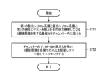
図2は、一実施形態に係るエッチング方法を示すフローチャートである。
まず、第1の酸化シリコン系膜と窒化シリコン系膜と第2の酸化シリコン系膜とをその順で積層してなる3層積層膜を有する基板Wをチャンバー10内に設ける(ステップST1)。
FIG. 2 is a flow chart illustrating an etching method according to one embodiment.
First, a substrate W having a three-layer laminated film formed by laminating a first silicon oxide film, a silicon nitride film, and a second silicon oxide film in that order is placed in the chamber 10 (step ST1).
次いで、チャンバー10内で、HF-NH3系ガスを用い、3層積層膜を各膜でガス比を調整しつつ一括してエッチングする(ステップST2)。
Next, in the
このとき、第1の酸化シリコン系膜、窒化シリコン系膜、および第2の酸化シリコン系膜のエッチングは、ローディングを最小限に抑制するために、各膜が良好な選択比で適切にエッチングされるように、ガス比を制御して実施される。また、各膜のエッチングは、載置台12の温度およびチャンバー10内の圧力を適切に制御して実施される。
At this time, the etching of the first silicon oxide film, the silicon nitride film, and the second silicon oxide film is performed by controlling the gas ratio so that each film is appropriately etched with a good selectivity ratio in order to minimize loading. In addition, the etching of each film is performed by appropriately controlling the temperature of the mounting table 12 and the pressure in the
酸化シリコン系膜および窒化シリコン系膜をHF-NH3系ガスでエッチングする際には、反応生成物としてケイフッ化アンモニウム(AFS)が生成される。このため、チャンバー10内で3層積層膜を構成する各膜を一括してエッチングするために、各膜のエッチングにおいて、HF-NH3系ガスを供給する操作と、チャンバー10内をパージする操作とを繰り返し行うサイクルエッチングを用いることが好ましい。これにより、HF-NH3系ガスを供給した際のAFSの生成と、パージによるAFSの昇華とが繰り返し行われ、エッチングを進行させることができる。繰り返し回数は、各膜の膜厚に応じて適宜設定される。
When etching a silicon oxide film and a silicon nitride film with HF-NH 3 -based gas, ammonium silicofluoride (AFS) is generated as a reaction product. Therefore, in order to collectively etch each film constituting the three-layer laminated film in the
以下、より具体的に説明する。
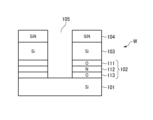
ステップST1において、基板Wは3層積層膜を有していればその構造は限定されないが、構造例として、例えば、図3に模式的に示すようなものを挙げることができる。図3の例では、基板Wは、基体(図示せず)上に、Si膜101が形成され、その上に、エッチング対象の3層積層膜であるONO積層膜102が形成されている。ONO積層膜102は、下から順に第2の酸化シリコン系膜113、窒化シリコン系膜112、および第1の酸化シリコン系膜111が積層して構成されている。第1の酸化シリコン系膜111、窒化シリコン系膜112、および第2の酸化シリコン系膜113のそれぞれの膜厚は、6~12nmの範囲であることが好ましい。ONO積層膜102の上には、Si膜103およびSiN膜104が形成され、Si膜103およびSiN膜104には、凹部(トレンチまたはホール)105が形成されている。なお、Si膜101,103はpoly-Si膜でもアモルファスSi膜(a-Si膜)でもよい。
This will be explained in more detail below.
In step ST1, the structure of the substrate W is not limited as long as it has a three-layer laminated film, but an example of the structure can be, for example, one as shown in FIG. 3. In the example of FIG. 3, the substrate W has a
図3の基板Wに、ステップST2の第1の酸化シリコン系膜111、窒化シリコン系膜112、および第2の酸化シリコン系膜113の一括エッチングを施すことにより、図4に示すように、下地のSi膜101が露出した状態となる。
By performing collective etching of the first
第1の酸化シリコン系膜111と第2の酸化シリコン系膜113は、SiとOとを主成分とし、添加物を含んでいてもよい。これらは同じ材料であってもよいが、異なる材料であることが好ましい。第1の酸化シリコン系膜としては、熱酸化膜(Th-SiO2膜)およびTEOS膜(CVD-SiO2膜)が例示される。TEOS膜とは、Siプリカーサとして、テトラエトキシシラン(TEOS)を用いてCVD法により形成された膜である。TEOS膜は、プラズマCVD法により形成したPTEOS膜であってもよい。第2の酸化シリコン系膜113としては、ALDにより成膜されたSiO2膜(ALD-SiO2膜)やSiON膜が例示される。これらは第1の酸化シリコン系膜111として用いる熱酸化膜やTEOS膜と比べて低密度の膜である。このように第2の酸化シリコン系膜113を第1の酸化シリコン系膜よりも低密度の膜とすることにより、第2の酸化シリコン系膜113を第1の酸化シリコン系膜111に対して選択的にエッチングすることができる。
The first
窒化シリコン系膜112は、SiとNとを主成分とし、添加物を含んでいてもよい。窒化シリコン系膜112としては、CVD法やALD法で成膜されたSiN膜(CVD-SiN膜、ALD-SiN膜)が例示される。
The
ステップST2においては、図5に示すように、第1の酸化シリコン系膜111をエッチングする段階(ST2-1)、窒化シリコン系膜112をエッチングする段階(ST2-2)、および第2の酸化シリコン系膜113をエッチングする段階(ST2-3)が実施される。これらの段階で所望のエッチングを行うために、酸化シリコン系膜をエッチングする段階であるST2-1およびST2-3と、窒化シリコン系膜をエッチングする段階であるST2-2とで、HF-NH3系ガスのガス比を調整する。 5, in step ST2, a stage of etching the first silicon oxide film 111 (ST2-1), a stage of etching the silicon nitride film 112 (ST2-2), and a stage of etching the second silicon oxide film 113 (ST2-3) are performed. In order to perform the desired etching in these stages, the gas ratio of the HF-NH 3 -based gas is adjusted in the stages ST2-1 and ST2-3 for etching the silicon oxide film and the stage ST2-2 for etching the silicon nitride film.
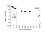
図6は、NH3ガスとHFガスの比率を変化させてSiO2膜(Th-SiO2膜)とSiN膜をエッチングした際の、HFガスおよびNH3ガスに対するHFガスの比(HFガス比;HF/(HF+NH3)×100(%)))と、SiNに対するSiO2の選択比(SiO2/SiN)との関係を示す図である。この図に示すように、SiO2膜は、NH3ガスがリッチの範囲においてエッチングが進行しやすく、HFガス比が20%以下で窒化シリコン膜に対して100以上の高選択比が得られることがわかる。ただし、HFガス比が3%未満になると反応が進行し難くなる。一方、SiN膜は、HFガスがリッチの範囲においてエッチングが進行しやすく、HFガス比が99%以上程度で高選択比が得られることがわかる。具体的には、HFガス比が100%でSiO2/SiNが0.01以下、つまりSiO2に対するSiNの選択比が100以上となっていることがわかる。
FIG. 6 is a diagram showing the relationship between the ratio of HF gas to HF gas and NH 3 gas (HF gas ratio; HF/(HF+NH 3 )×100(%)) and the selectivity of SiO 2 to SiN (SiO 2 /SiN) when etching a SiO 2 film (Th-SiO 2 film) and a SiN film by changing the ratio of
したがって、酸化シリコン系膜をエッチングする段階であるST2-1およびST2-3では、HFガス比が3~20%であることが好ましい。より好ましくは3~9%の範囲である。この範囲で選択比に加え十分なエッチング量を得ることができる。 Therefore, in the steps ST2-1 and ST2-3 where the silicon oxide film is etched, the HF gas ratio is preferably 3 to 20%. More preferably, it is in the range of 3 to 9%. In this range, a sufficient amount of etching can be obtained in addition to the selectivity ratio.
一方、窒化シリコン系膜をエッチングする段階であるST2-2では、HFガス比が99%以上であることが好ましい。より好ましくはHFガス比が100%である。 On the other hand, in ST2-2, which is the stage where the silicon nitride film is etched, it is preferable that the HF gas ratio is 99% or more. More preferably, the HF gas ratio is 100%.
ステップST2のエッチング工程において、第2の酸化シリコン系膜113をエッチングする段階であるST2-3を実施するに際しては、第1の酸化シリコン系膜111に対して選択的にエッチングされることが好ましい。第1の酸化シリコン系膜111がTh-SiO2膜またはCVD-SiO2膜で、第2の酸化シリコン系膜113がALD-SiO2膜またはSiON膜の場合には、以下により、第2の酸化シリコン系膜113を選択的にエッチングすることができる。すなわち、第2の酸化シリコン系膜113をエッチングする際のHFガスの比率を、第1の酸化シリコン系膜111のエッチングよりも減少させることにより、第2の酸化シリコン系膜113を第1の酸化シリコン系膜111に対して選択的にエッチングすることができる。
In the etching process of step ST2, when performing ST2-3, which is a stage of etching the second
以上のような好ましいガス比率で各膜をエッチングする際のガス流量は、以下のような範囲が好ましい。
・第1の酸化シリコン系膜111のエッチング段階(ST2-1)
HFガス:50~100sccm
NH3ガス:450~550sccm
N2ガス+Arガス:300~600sccm
・窒化シリコン系膜112のエッチング段階(ST2-2)
HFガス:800~1000sccm
NH3ガス:0~10sccm
N2ガス+Arガス:300~600sccm
・第2の酸化シリコン系膜113のエッチング段階(ST2-3)
HFガス:30~50sccm(第1の酸化シリコン系膜のエッチングの際よりも少なくする。)
NH3ガス:450~550sccm
N2ガス+Arガス:300~600sccm
The gas flow rates when etching each film with the above-mentioned preferable gas ratios are preferably in the following ranges.
Etching step of the first silicon oxide film 111 (ST2-1)
HF gas: 50 to 100 sccm
NH3 gas: 450 to 550 sccm
N2 gas + Ar gas: 300 to 600 sccm
Etching step of silicon nitride film 112 (ST2-2)
HF gas: 800 to 1000 sccm
NH3 gas: 0 to 10 sccm
N2 gas + Ar gas: 300 to 600 sccm
Etching step of the second silicon oxide film 113 (ST2-3)
HF gas: 30 to 50 sccm (less than that in the etching of the first silicon oxide film)
NH3 gas: 450 to 550 sccm
N2 gas + Ar gas: 300 to 600 sccm
ステップST2における圧力に関しては、第1および第2の酸化シリコン系膜111,113をエッチングする段階(ST2-1およびST2-3)においては、相対的に低圧にすることが好ましい。これにより、第1および第2の酸化シリコン系膜111,113を窒化シリコン系膜112に対して選択的にエッチングすることができる。一方、窒化シリコン系膜112をエッチングする段階(ST2-2)においては、相対的に高圧にすることが好ましい。これにより、窒化シリコン系膜112を第1および第2の酸化シリコン系膜111,113に対して選択的にエッチングすることができる。
Regarding the pressure in step ST2, it is preferable to set the pressure to a relatively low level in the stages (ST2-1 and ST2-3) in which the first and second
より好ましくは、第1および第2の酸化シリコン系膜111,113をエッチングする段階(ST2-1およびST2-3)においては5Torr(667Pa)以下であり、窒化シリコン系膜112をエッチングする段階(ST2-2)においては5~100Torr(667~13332Pa)である。
More preferably, the pressure is 5 Torr (667 Pa) or less in the steps (ST2-1 and ST2-3) of etching the first and second
窒化シリコン系膜112をエッチングする段階(ST2-2)の基板温度(載置台温度)は80~100℃が好ましく、90~100℃がより好ましい。温度をこの範囲にすることにより、窒化シリコン系膜112を現実的なエッチング量で第1および第2の酸化シリコン膜111,113に対して高選択比でエッチングすることができる。
The substrate temperature (mounting table temperature) in the step (ST2-2) of etching the
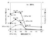
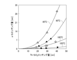
図7は、HFガス100%、圧力20Torrおよび50Torrで、ALD-SiN膜とTh-SiO2膜を、載置台温度を90~120℃で変化させてエッチングした際における、載置台温度と各膜のエッチング量との関係、およびALD-SiN膜のTh-SiO2膜に対する選択比を示す図である。この図に示すように、90~100℃において、SiN膜を現実的なエッチング量で、かつSiO2膜に対して高選択比でエッチング可能である。105℃においては、選択比は高いがエッチング量が少なくなってしまう。 7 is a diagram showing the relationship between the temperature of the mounting table and the etching amount of each film, and the selectivity of the ALD-SiN film to the Th-SiO 2 film, when an ALD-SiN film and a Th-SiO 2 film are etched with 100% HF gas at pressures of 20 Torr and 50 Torr and the mounting table temperature is changed from 90 to 120° C. As shown in this figure, at 90 to 100° C., it is possible to etch the SiN film with a realistic etching amount and with a high selectivity to the SiO 2 film. At 105° C., the selectivity is high, but the etching amount is small.
また、図3の構造の基板Wにおいては、ONO積層膜102の各膜のエッチングにおいてSi膜101および103に対する選択比が高いことが求められるが、温度が低いとSiがエッチングされてしまう。そのモデルは以下の通りである。図8はONO積層膜をエッチングする際にSiがエッチングされるモデルを示す図である。例えば、第1および第2の酸化シリコン系膜111,113をエッチングする際には、図8に示すように、HFガスおよびNH3ガスによりエッチングを行ってAFSが生成する過程でH2Oが発生する。そして、温度が低いとH2Oが残存し、H2Oと導入ガスであるNH3とが反応して、Siがアルカリエッチングされてしまう。この反応を抑制するためには、基板温度を上昇させてH2Oを除去することが好ましい。図9は、各温度でHFガスとNH3ガスによりTh-SiO2膜をエッチングしたときの、Th-SiO2膜のエッチング量とa-Si膜のエッチング量との関係を示す図である。この図に示すように、85℃ではTh-SiO2膜のa-Si膜に対する選択比が低い傾向にあるが、90℃においてはある程度高い選択比が得られており、温度が上昇するに従ってa-Siのエッチング量が低下している。したがって、ステップST2において各膜をSiに対して選択的にエッチングするためには、載置台温度(基板温度)は90℃以上が好ましい。上述したように、105℃ではSiN膜のエッチング量が少ないため、90~100℃が好ましい。
In addition, in the substrate W having the structure of FIG. 3, a high selectivity ratio to the
以上のSiN膜のSiO2膜に対する選択性およびSiO2膜のSi膜に対する選択性の結果を考慮すると、ステップST2のONO積層膜102のエッチングの際の基板温度(載置台温度)は、80~100℃が好ましく、90~100℃がより好ましい。この範囲内で各膜をエッチングする段階(ST2-1~ST2-3)で温度を変化させてもよいが、実質的に同一温度とすることが好ましい。
Considering the above results of the selectivity of the SiN film to the SiO 2 film and the selectivity of the SiO 2 film to the Si film, the substrate temperature (temperature of the mounting table) during etching of the ONO laminated
ステップST2における各膜をエッチングする段階(ST2-1~ST2-3)においては、上述したように、HF-NH3系ガスを供給して反応生成物を生成させる操作と、チャンバー10内をパージして反応生成物を昇華させる操作とを繰り返し実施するサイクルエッチングが好ましい。また、ONO積層膜102のエッチングが終了した後は、基板Wをチャンバー10から搬出して加熱装置により残渣除去のための加熱処理を行うことが好ましい。
In the stages (ST2-1 to ST2-3) of etching each film in step ST2, as described above, it is preferable to perform cycle etching in which an operation of supplying HF-NH 3 -based gas to generate a reaction product and an operation of purging the
各膜のサイクルエッチの際の1回のHF-NH3系ガスを供給する操作の時間は、20~60secの範囲が好ましい。また、1回のパージする操作の時間は、十分にAFSを除去する観点から3min以上が好ましく、3~5minの範囲がより好ましい。ただし、ONO積層膜102のエッチングが終了した後に残渣除去のための加熱処理を行う場合は、最後の第2の酸化シリコン系膜113をエッチングする段階(ST2-3)の際のパージ時間は短くてよく、30~60secの範囲が好ましい。
The time for one operation of supplying HF- NH3- based gas during cycle etching of each film is preferably in the range of 20 to 60 seconds. Also, the time for one purge operation is preferably 3 minutes or more from the viewpoint of sufficiently removing AFS, and more preferably in the range of 3 to 5 minutes. However, when a heat treatment for removing residue is performed after etching of the ONO laminated
また、パージする操作は、チャンバー10内を真空引きするのみであってもよいし、真空引きしながらパージガスを供給してもよい。パージガスとしては、Arガス供給源52および/またはN2ガス供給源54から供給されるArガスおよび/またはN2ガスを用いることができる。AFSを効果的に排出するためには真空引きのみを実施することが好ましい。
The purging operation may be performed by simply drawing a vacuum inside the
パージする操作の際には、基板Wに生成されたAFSの昇華が進行し得る温度になるように載置台12の温度が設定される。載置台12の温度が上述した80~100℃の温度範囲であれば、サイクルエッチングにおけるパージする操作で反応生成物であるAFSを十分に除去可能である。 During the purging operation, the temperature of the mounting table 12 is set to a temperature at which sublimation of the AFS generated on the substrate W can proceed. If the temperature of the mounting table 12 is within the above-mentioned temperature range of 80 to 100°C, the AFS, which is a reaction product, can be sufficiently removed by the purging operation in the cycle etching.
図3の構造の基板Wにおいては、ONO積層膜102をエッチングする際にSiN膜104に対する選択性も要求される。SiN膜104はONO積層膜102の窒化シリコン系膜112と同種の膜であるが、窒化シリコン系膜112をサイクルエッチングする際のパージ時間を長くしてAFSとH2Oを極力低減することにより、SiN膜104のロスを低減することができる。これにより、窒化シリコン系膜112をエッチングする際にSiN膜104に対する選択性も確保することができる。この際のパージ時間は3~5minの範囲であることが好ましい。
3, selectivity to the
各膜のエッチングが終了した後は、チャンバー10内をパージする。パージガスとしては、Arガス供給源52および/またはN2ガス供給源54から供給されるArガスおよび/またはN2ガスを用いることができる。第2の酸化シリコン系膜113のエッチングが終了した後、このようにチャンバーのパージを行い、その後、基板Wをチャンバー10から搬出する。
After etching of each film is completed, the
上述の特許文献1に示すように、SiO2膜をHFガスおよびNH3ガスによりガスエッチングすることは従来から知られている。一方、半導体装置の構造中には、本実施形態で対象とするようなONO積層膜が多用されており、ONO積層膜のエッチングが求められる。ONO積層膜のエッチングに際しては、ローディングを最小限に抑制するため、SiO2膜とSiN膜を高い選択性でエッチングする必要があり、従来、SiO2膜のガスエッチングとSiN膜のウエットエッチングが併用されてきた。
As shown in the above-mentioned
これに対し、本実施形態では、ONO積層膜を構成する第1の酸化シリコン系膜、窒化シリコン系膜、第2の酸化シリコン系膜のガス比率等の条件を最適化し、さらにサイクルエッチを適用することにより、ONO積層膜をガスエッチングによる一括エッチングでエッチングすることが可能となる。これにより、ONO積層を従来よりも簡易な工程により高スループットでエッチングすることができる。 In contrast, in this embodiment, the conditions such as the gas ratio of the first silicon oxide film, silicon nitride film, and second silicon oxide film that make up the ONO laminate film are optimized, and cycle etching is further applied, making it possible to etch the ONO laminate film in a single gas etching process. This allows the ONO laminate to be etched with a high throughput using a simpler process than before.
また、ONO積層膜に隣接する位置にSi膜が存在する場合には、Si膜に対して高選択比でONO積層膜をエッチングすることが要求される。特に、図3のように、ONO積層膜102の下地となるSi膜101は、トランジスタの機能部(チャネル等)となることが多く、ONO積層膜102をエッチングした際に極力エッチングされないことが要求される。これに対して、本実施形態では、上述したように、ONO積層膜をSi膜に対しても高選択比でエッチングすることができる。
In addition, when a Si film is present adjacent to the ONO laminate film, it is required to etch the ONO laminate film with a high selectivity to the Si film. In particular, as shown in FIG. 3, the
<他の適用>
以上、実施形態について説明したが、今回開示された実施形態は、全ての点で例示であって制限的なものではないと考えられるべきである。上記の実施形態は、添付の特許請求の範囲およびその主旨を逸脱することなく、様々な形態で省略、置換、変更されてもよい。
<Other applications>
Although the embodiments have been described above, the embodiments disclosed herein should be considered to be illustrative and not restrictive in all respects. The above-described embodiments may be omitted, substituted, or modified in various forms without departing from the scope and spirit of the appended claims.
例えば、上記実施形態の装置は例示に過ぎず、種々の構成の装置を適用することができる。また、基板として半導体ウエハを例示したが、FPD(フラットパネルディスプレイ)基板や、セラミックス基板等の他の基板であってもよい。 For example, the device in the above embodiment is merely an example, and devices of various configurations can be applied. Also, although a semiconductor wafer is exemplified as the substrate, other substrates such as an FPD (flat panel display) substrate or a ceramic substrate may also be used.
1;エッチング装置
10;チャンバー
12;載置台
13;ガス供給機構
14;排気機構
26;シャワーヘッド
45;温調器
51;HFガス供給源
53;NH3ガス供給源
80;制御部
101,103;Si膜
102;ONO積層膜
104;SiN膜
105;凹部
111;第1の酸化シリコン系膜
112;窒化シリコン系膜
113;第2の酸化シリコン系膜
W;基板
REFERENCE SIGNS
Claims (18)
前記チャンバー内で、HF-NH3系ガスを用い、前記3層積層膜を、各膜におけるガス比を調整しつつ一括してエッチングする工程と、
を有する、エッチング方法。 Providing a substrate having a three-layer laminated film formed by laminating a first silicon oxide film, a silicon nitride film, and a second silicon oxide film in a chamber;
a step of simultaneously etching the three-layer stacked film in the chamber using an HF-NH3 - based gas while adjusting the gas ratio for each film;
The etching method according to claim 1,
前記第1の酸化シリコン系膜および前記窒化シリコン系膜の前記パージする操作の時間を3~5minとし、前記第2の酸化シリコン系膜の前記パージする操作の時間を30~60secとする、請求項2に記載のエッチング方法。 The method further includes a step of removing the substrate from the chamber after the etching step, and a step of heating the removed substrate to remove residues,
3. The etching method according to claim 2, wherein the purging operation time for the first silicon oxide film and the silicon nitride film is 3 to 5 minutes, and the purging operation time for the second silicon oxide film is 30 to 60 seconds.
前記第1の酸化シリコン系膜は、熱酸化膜またはTEOS膜であり、前記第2の酸化シリコン系膜は、ALDで成膜された酸化シリコン膜、またはSiON膜である、請求項1から請求項10のいずれか一項に記載のエッチング方法。 Etching of the three-layer stacked film starts from the first silicon oxide film and ends at the second silicon oxide film;
11. The etching method according to claim 1, wherein the first silicon oxide-based film is a thermal oxide film or a TEOS film, and the second silicon oxide-based film is a silicon oxide film formed by ALD or a SiON film.
前記チャンバー内で前記基板を載置する載置台と、
前記チャンバー内に塩基性ガスとフッ素含有ガスを供給するガス供給部と、
前記チャンバー内を排気する排気部と、
前記載置台上の基板の温度を調節する温調部と、
制御部と、
を具備し、
前記制御部は、前記チャンバー内の前記載置台に載置された前記基板に対し、HF-NH3系ガスを用い、前記3層積層膜が、各膜におけるガス比を調整しつつ一括してエッチングされるように、前記ガス供給部と、前記排気部と、前記温調部とを制御する、エッチング装置。 a chamber for accommodating a substrate having a three-layer laminated film formed by laminating a first silicon oxide-based film, a silicon nitride-based film, and a second silicon oxide-based film;
a mounting table on which the substrate is placed within the chamber;
a gas supply unit for supplying a basic gas and a fluorine-containing gas into the chamber;
an exhaust unit that exhausts the inside of the chamber;
a temperature control unit for controlling the temperature of the substrate on the mounting table;
A control unit;
Equipped with
the control unit controls the gas supply unit, the exhaust unit, and the temperature adjustment unit so that the three-layer stacked film is etched all at once while adjusting the gas ratio for each film by using an HF- NH3- based gas for the substrate placed on the mounting table in the chamber.
前記制御部は、前記第2の酸化シリコン系膜のエッチングの際に、HFガス流量が前記第1の酸化シリコン系膜のエッチングの際よりも少なくなるように制御する、請求項13から請求項17のいずれか一項に記載のエッチング装置。
Etching of the three-layer stacked film starts from the first silicon oxide film and ends at the second silicon oxide film, the first silicon oxide film is a thermal oxide film or a TEOS film, and the second silicon oxide film is a silicon oxide film formed by ALD or a SiON film,
18. The etching apparatus according to claim 13, wherein the control unit controls a HF gas flow rate during etching of the second silicon oxide-based film to be lower than a flow rate during etching of the first silicon oxide-based film.
Priority Applications (7)
| Application Number | Priority Date | Filing Date | Title |
|---|---|---|---|
| JP2020188278A JP7561579B2 (en) | 2020-11-11 | 2020-11-11 | Etching method and etching apparatus |
| KR1020257035567A KR20250158820A (en) | 2020-11-11 | 2021-10-28 | Etching method and etching apparatus |
| KR1020237011149A KR102877738B1 (en) | 2020-11-11 | 2021-10-28 | Etching method and etching device |
| PCT/JP2021/039777 WO2022102421A1 (en) | 2020-11-11 | 2021-10-28 | Etching method and etching apparatus |
| US18/247,669 US12381090B2 (en) | 2020-11-11 | 2021-10-28 | Etching method and etching apparatus |
| CN202180066737.1A CN116325081A (en) | 2020-11-11 | 2021-10-28 | Etching method and etching apparatus |
| US19/262,194 US20250336682A1 (en) | 2020-11-11 | 2025-07-08 | Etching method and etching apparatus |
Applications Claiming Priority (1)
| Application Number | Priority Date | Filing Date | Title |
|---|---|---|---|
| JP2020188278A JP7561579B2 (en) | 2020-11-11 | 2020-11-11 | Etching method and etching apparatus |
Publications (2)
| Publication Number | Publication Date |
|---|---|
| JP2022077419A JP2022077419A (en) | 2022-05-23 |
| JP7561579B2 true JP7561579B2 (en) | 2024-10-04 |
Family
ID=81601106
Family Applications (1)
| Application Number | Title | Priority Date | Filing Date |
|---|---|---|---|
| JP2020188278A Active JP7561579B2 (en) | 2020-11-11 | 2020-11-11 | Etching method and etching apparatus |
Country Status (5)
| Country | Link |
|---|---|
| US (2) | US12381090B2 (en) |
| JP (1) | JP7561579B2 (en) |
| KR (2) | KR20250158820A (en) |
| CN (1) | CN116325081A (en) |
| WO (1) | WO2022102421A1 (en) |
Families Citing this family (5)
| Publication number | Priority date | Publication date | Assignee | Title |
|---|---|---|---|---|
| KR102779338B1 (en) * | 2021-10-06 | 2025-03-12 | 주식회사 테스 | Method of processing substrate |
| JP2024062579A (en) * | 2022-10-25 | 2024-05-10 | 東京エレクトロン株式会社 | SUBSTRATE PROCESSING METHOD AND SUBSTRATE PROCESSING APPARATUS |
| CN118525355A (en) * | 2022-12-19 | 2024-08-20 | 株式会社日立高新技术 | Etching method |
| WO2025150427A1 (en) * | 2024-01-09 | 2025-07-17 | 東京エレクトロン株式会社 | Etching method and plasma processing system |
| JP2026044293A (en) * | 2024-08-30 | 2026-03-12 | 東京エレクトロン株式会社 | Etching method and etching apparatus |
Citations (3)
| Publication number | Priority date | Publication date | Assignee | Title |
|---|---|---|---|---|
| JP2014060220A (en) | 2012-09-14 | 2014-04-03 | Tokyo Electron Ltd | Etching apparatus and etching method |
| JP2016154209A (en) | 2015-02-16 | 2016-08-25 | 東京エレクトロン株式会社 | Substrate processing method and substrate processing apparatus |
| JP2018207088A (en) | 2017-05-30 | 2018-12-27 | 東京エレクトロン株式会社 | Etching method |
Family Cites Families (7)
| Publication number | Priority date | Publication date | Assignee | Title |
|---|---|---|---|---|
| JP3897518B2 (en) * | 2000-05-31 | 2007-03-28 | 芝浦メカトロニクス株式会社 | Etching method of silicon nitride film |
| JP4833512B2 (en) | 2003-06-24 | 2011-12-07 | 東京エレクトロン株式会社 | To-be-processed object processing apparatus, to-be-processed object processing method, and to-be-processed object conveyance method |
| JP5084250B2 (en) | 2006-12-26 | 2012-11-28 | 東京エレクトロン株式会社 | Gas processing apparatus, gas processing method, and storage medium |
| TW201108324A (en) * | 2009-03-24 | 2011-03-01 | Tokyo Electron Ltd | A method for processing a substrate |
| JP6080166B2 (en) * | 2011-08-25 | 2017-02-15 | 株式会社Screenホールディングス | Pattern formation method |
| JP5968130B2 (en) | 2012-07-10 | 2016-08-10 | 東京エレクトロン株式会社 | Plasma processing method and plasma processing apparatus |
| JP6405958B2 (en) * | 2013-12-26 | 2018-10-17 | 東京エレクトロン株式会社 | Etching method, storage medium, and etching apparatus |
-
2020
- 2020-11-11 JP JP2020188278A patent/JP7561579B2/en active Active
-
2021
- 2021-10-28 WO PCT/JP2021/039777 patent/WO2022102421A1/en not_active Ceased
- 2021-10-28 CN CN202180066737.1A patent/CN116325081A/en active Pending
- 2021-10-28 US US18/247,669 patent/US12381090B2/en active Active
- 2021-10-28 KR KR1020257035567A patent/KR20250158820A/en active Pending
- 2021-10-28 KR KR1020237011149A patent/KR102877738B1/en active Active
-
2025
- 2025-07-08 US US19/262,194 patent/US20250336682A1/en active Pending
Patent Citations (3)
| Publication number | Priority date | Publication date | Assignee | Title |
|---|---|---|---|---|
| JP2014060220A (en) | 2012-09-14 | 2014-04-03 | Tokyo Electron Ltd | Etching apparatus and etching method |
| JP2016154209A (en) | 2015-02-16 | 2016-08-25 | 東京エレクトロン株式会社 | Substrate processing method and substrate processing apparatus |
| JP2018207088A (en) | 2017-05-30 | 2018-12-27 | 東京エレクトロン株式会社 | Etching method |
Also Published As
| Publication number | Publication date |
|---|---|
| WO2022102421A1 (en) | 2022-05-19 |
| US20250336682A1 (en) | 2025-10-30 |
| KR102877738B1 (en) | 2025-10-28 |
| KR20230058504A (en) | 2023-05-03 |
| US20240006187A1 (en) | 2024-01-04 |
| KR20250158820A (en) | 2025-11-06 |
| CN116325081A (en) | 2023-06-23 |
| JP2022077419A (en) | 2022-05-23 |
| US12381090B2 (en) | 2025-08-05 |
Similar Documents
| Publication | Publication Date | Title |
|---|---|---|
| JP7561579B2 (en) | Etching method and etching apparatus | |
| US12494364B2 (en) | Method of manufacturing semiconductor device, substrate processing method, substrate processing apparatus, and recording medium | |
| KR102368311B1 (en) | Method of manufacturing semiconductor device, substrate processing method, substrate processing apparatus, and program | |
| US11735442B2 (en) | Method of operating substrate processing apparatus, method of manufacturing semiconductor device, substrate processing apparatus, and recording medium | |
| CN110783188B (en) | Etching method and etching device | |
| KR102288228B1 (en) | Method of manufacturing semiconductor device, substrate processing apparatus, and program | |
| JP7778183B2 (en) | Etching method and etching apparatus | |
| TW201624564A (en) | Etching method and storage medium | |
| TW202234553A (en) | Substrate processing apparatus, plasma generating device, method of manufacturing semiconductor device, and substrate processing method | |
| TW201941283A (en) | Etching method | |
| JPWO2019012797A1 (en) | Semiconductor device manufacturing method, substrate processing apparatus, and program | |
| JPWO2019186637A1 (en) | Semiconductor device manufacturing methods, substrate processing devices and programs | |
| US20240035155A1 (en) | Cleaning method, method of manufacturing semiconductor device, substrate processing apparatus, and recording medium | |
| JP2023065305A (en) | Deposition method and deposition system | |
| JP7822166B2 (en) | Gas treatment method and gas treatment device | |
| WO2023127137A1 (en) | Substrate processing method, production method for semiconductor device, substrate processing device, and program |
Legal Events
| Date | Code | Title | Description |
|---|---|---|---|
| A621 | Written request for application examination |
Free format text: JAPANESE INTERMEDIATE CODE: A621 Effective date: 20230814 |
|
| TRDD | Decision of grant or rejection written | ||
| A01 | Written decision to grant a patent or to grant a registration (utility model) |
Free format text: JAPANESE INTERMEDIATE CODE: A01 Effective date: 20240827 |
|
| A61 | First payment of annual fees (during grant procedure) |
Free format text: JAPANESE INTERMEDIATE CODE: A61 Effective date: 20240924 |
|
| R150 | Certificate of patent or registration of utility model |
Ref document number: 7561579 Country of ref document: JP Free format text: JAPANESE INTERMEDIATE CODE: R150 |