JP7547526B2 - 複数計算における高スループットのためのシステムおよび方法 - Google Patents
複数計算における高スループットのためのシステムおよび方法 Download PDFInfo
- Publication number
- JP7547526B2 JP7547526B2 JP2023033382A JP2023033382A JP7547526B2 JP 7547526 B2 JP7547526 B2 JP 7547526B2 JP 2023033382 A JP2023033382 A JP 2023033382A JP 2023033382 A JP2023033382 A JP 2023033382A JP 7547526 B2 JP7547526 B2 JP 7547526B2
- Authority
- JP
- Japan
- Prior art keywords
- unit
- data
- gpu
- axi
- dsdu
- Prior art date
- Legal status (The legal status is an assumption and is not a legal conclusion. Google has not performed a legal analysis and makes no representation as to the accuracy of the status listed.)
- Active
Links
Images


Classifications
-
- G—PHYSICS
- G06—COMPUTING OR CALCULATING; COUNTING
- G06F—ELECTRIC DIGITAL DATA PROCESSING
- G06F13/00—Interconnection of, or transfer of information or other signals between, memories, input/output devices or central processing units
- G06F13/14—Handling requests for interconnection or transfer
-
- G—PHYSICS
- G06—COMPUTING OR CALCULATING; COUNTING
- G06F—ELECTRIC DIGITAL DATA PROCESSING
- G06F8/00—Arrangements for software engineering
- G06F8/40—Transformation of program code
- G06F8/41—Compilation
- G06F8/44—Encoding
- G06F8/441—Register allocation; Assignment of physical memory space to logical memory space
-
- G—PHYSICS
- G06—COMPUTING OR CALCULATING; COUNTING
- G06F—ELECTRIC DIGITAL DATA PROCESSING
- G06F9/00—Arrangements for program control, e.g. control units
- G06F9/06—Arrangements for program control, e.g. control units using stored programs, i.e. using an internal store of processing equipment to receive or retain programs
- G06F9/30—Arrangements for executing machine instructions, e.g. instruction decode
- G06F9/30003—Arrangements for executing specific machine instructions
- G06F9/3004—Arrangements for executing specific machine instructions to perform operations on memory
- G06F9/30043—LOAD or STORE instructions; Clear instruction
-
- G—PHYSICS
- G06—COMPUTING OR CALCULATING; COUNTING
- G06F—ELECTRIC DIGITAL DATA PROCESSING
- G06F9/00—Arrangements for program control, e.g. control units
- G06F9/06—Arrangements for program control, e.g. control units using stored programs, i.e. using an internal store of processing equipment to receive or retain programs
- G06F9/30—Arrangements for executing machine instructions, e.g. instruction decode
- G06F9/30098—Register arrangements
-
- G—PHYSICS
- G06—COMPUTING OR CALCULATING; COUNTING
- G06F—ELECTRIC DIGITAL DATA PROCESSING
- G06F9/00—Arrangements for program control, e.g. control units
- G06F9/06—Arrangements for program control, e.g. control units using stored programs, i.e. using an internal store of processing equipment to receive or retain programs
- G06F9/30—Arrangements for executing machine instructions, e.g. instruction decode
- G06F9/38—Concurrent instruction execution, e.g. pipeline or look ahead
- G06F9/3836—Instruction issuing, e.g. dynamic instruction scheduling or out of order instruction execution
- G06F9/3851—Instruction issuing, e.g. dynamic instruction scheduling or out of order instruction execution from multiple instruction streams, e.g. multistreaming
-
- G—PHYSICS
- G06—COMPUTING OR CALCULATING; COUNTING
- G06F—ELECTRIC DIGITAL DATA PROCESSING
- G06F9/00—Arrangements for program control, e.g. control units
- G06F9/06—Arrangements for program control, e.g. control units using stored programs, i.e. using an internal store of processing equipment to receive or retain programs
- G06F9/30—Arrangements for executing machine instructions, e.g. instruction decode
- G06F9/38—Concurrent instruction execution, e.g. pipeline or look ahead
- G06F9/3877—Concurrent instruction execution, e.g. pipeline or look ahead using a slave processor, e.g. coprocessor
-
- G—PHYSICS
- G06—COMPUTING OR CALCULATING; COUNTING
- G06F—ELECTRIC DIGITAL DATA PROCESSING
- G06F9/00—Arrangements for program control, e.g. control units
- G06F9/06—Arrangements for program control, e.g. control units using stored programs, i.e. using an internal store of processing equipment to receive or retain programs
- G06F9/30—Arrangements for executing machine instructions, e.g. instruction decode
- G06F9/38—Concurrent instruction execution, e.g. pipeline or look ahead
- G06F9/3885—Concurrent instruction execution, e.g. pipeline or look ahead using a plurality of independent parallel functional units
- G06F9/3888—Concurrent instruction execution, e.g. pipeline or look ahead using a plurality of independent parallel functional units controlled by a single instruction for multiple threads [SIMT] in parallel
-
- G—PHYSICS
- G06—COMPUTING OR CALCULATING; COUNTING
- G06T—IMAGE DATA PROCESSING OR GENERATION, IN GENERAL
- G06T1/00—General purpose image data processing
- G06T1/20—Processor architectures; Processor configuration, e.g. pipelining
-
- G—PHYSICS
- G06—COMPUTING OR CALCULATING; COUNTING
- G06T—IMAGE DATA PROCESSING OR GENERATION, IN GENERAL
- G06T1/00—General purpose image data processing
- G06T1/60—Memory management
-
- G—PHYSICS
- G06—COMPUTING OR CALCULATING; COUNTING
- G06F—ELECTRIC DIGITAL DATA PROCESSING
- G06F12/00—Accessing, addressing or allocating within memory systems or architectures
- G06F12/02—Addressing or allocation; Relocation
- G06F12/08—Addressing or allocation; Relocation in hierarchically structured memory systems, e.g. virtual memory systems
- G06F12/0802—Addressing of a memory level in which the access to the desired data or data block requires associative addressing means, e.g. caches
- G06F12/0806—Multiuser, multiprocessor or multiprocessing cache systems
-
- G—PHYSICS
- G06—COMPUTING OR CALCULATING; COUNTING
- G06F—ELECTRIC DIGITAL DATA PROCESSING
- G06F13/00—Interconnection of, or transfer of information or other signals between, memories, input/output devices or central processing units
- G06F13/14—Handling requests for interconnection or transfer
- G06F13/20—Handling requests for interconnection or transfer for access to input/output bus
- G06F13/28—Handling requests for interconnection or transfer for access to input/output bus using burst mode transfer, e.g. direct memory access DMA, cycle steal
- G06F13/30—Handling requests for interconnection or transfer for access to input/output bus using burst mode transfer, e.g. direct memory access DMA, cycle steal with priority control
-
- G—PHYSICS
- G06—COMPUTING OR CALCULATING; COUNTING
- G06F—ELECTRIC DIGITAL DATA PROCESSING
- G06F13/00—Interconnection of, or transfer of information or other signals between, memories, input/output devices or central processing units
- G06F13/38—Information transfer, e.g. on bus
- G06F13/40—Bus structure
- G06F13/4004—Coupling between buses
- G06F13/4022—Coupling between buses using switching circuits, e.g. switching matrix, connection or expansion network
-
- G—PHYSICS
- G06—COMPUTING OR CALCULATING; COUNTING
- G06F—ELECTRIC DIGITAL DATA PROCESSING
- G06F2212/00—Indexing scheme relating to accessing, addressing or allocation within memory systems or architectures
- G06F2212/62—Details of cache specific to multiprocessor cache arrangements
- G06F2212/621—Coherency control relating to peripheral accessing, e.g. from DMA or I/O device
Landscapes
- Engineering & Computer Science (AREA)
- Theoretical Computer Science (AREA)
- Software Systems (AREA)
- Physics & Mathematics (AREA)
- General Physics & Mathematics (AREA)
- General Engineering & Computer Science (AREA)
- Multimedia (AREA)
- Image Processing (AREA)
- Memory System Of A Hierarchy Structure (AREA)
- Multi Processors (AREA)
- Advance Control (AREA)
- Mathematical Physics (AREA)
- Computer Hardware Design (AREA)
Description
Claims (6)
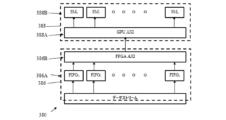
- データのストリームを受信するように構成され、前記データのストリームを、データ部分に分割し、前記データ部分の各々を、複数の先入れ先出し(FIFO)レジスタの1つを通過させるように構成された、複数の前記FIFOレジスタを備えたアレイと、
前記データ部分を受信するように構成された、第1のアドバンスト・イクステンシブル・インタフェース(AXI)ユニットと、
を備えたデータ・ストリーム・デバイダ・ユニット(DSDU)(304)と、
前記第1のAXIユニットからデータ部分を受信するように構成された、第2のアドバンスト・イクステンシブル・インタフェース(AXI)ユニットと、
それぞれのFIFOレジスタから各データ部分を受信するように構成され、前記受信したデータ部分を処理するように構成された、複数のストリーミングマルチプロセッサ(SM)と、
を備えたグラフィックプロセッシングユニット(GPU)と、
を備えた、GPUでの処理がまだ施されていない未処理データを処理する回路。 - 前記DSDU内のFIFOレジスタは、前記DSDU内の、前記FIFOレジスタに割り当てられた第1のAXIユニットと、前記GPU内の、前記FIFOレジスタに割り当てられた第2のAXIユニットを介して前記GPU内の、前記FIFOレジスタに割り当てられたSMに接続される、請求項1に記載の回路。
- 前記DSDU内の、前記FIFOレジスタの各々は、前記DSDU内の、第1の共通AXIユニット、および前記GPU内の、共通AXIユニットを介して、前記GPU内の、前記FIFOレジスタに割り当てられたSMに接続される、請求項1に記載の回路。
- グラフィックプロセッサユニット(GPU)での処理がまだ施されていない未処理データのストリームを受信するステップと、
前記ストリームを複数のデータ部分に分割するステップと、
データストリームデバイダユニット(DSDU)の特定のFIFOレジスタを介して各データ部分を通過させるステップと、
前記特定のFIFOレジスタからのデータ部分を、処理のためにグラフィックプロセッサユニット(GPU)内の、前記特定のFIFOレジスタに割り当てられたストリーミングマルチプロセッサ(SM)に転送するステップと、
を備え、
前記データ部分は、前記DSDU内の、第1のアドバンスト・イクステンシブル・インタフェース(AXI)ユニットと、前記GPU内の、第2のアドバンスト・イクステンシブル・インタフェース(AXI)ユニットを介して転送される、
大容量のデータを効率的に処理する方法。 - 特定のFIFOレジスタから受信したデータ部分は、前記DSDU内の、前記FIFOレジスタに割り当てられた第1のAXIユニットと、前記GPU内の、前記FIFOレジスタに割り当てられた第2のAXIユニットを介して前記GPU内の、前記特定のFIFOレジスタに割り当てられたSMに転送される、請求項4に記載の方法。
- FIFOレジスタから受信した前記データ部分の各々は、前記DSDU内の、共通の第1のAXIユニットと、前記GPU内の、共通の第2のAXIユニットを介して、前記GPU内の、前記特定のFIFOレジスタに割り当てられたSMに転送される、請求項4に記載の方法。
Applications Claiming Priority (4)
| Application Number | Priority Date | Filing Date | Title |
|---|---|---|---|
| US201762552475P | 2017-08-31 | 2017-08-31 | |
| US62/552,475 | 2017-08-31 | ||
| JP2020512508A JP2020532795A (ja) | 2017-08-31 | 2018-08-30 | 複数計算における高スループットのためのシステムおよび方法 |
| PCT/IL2018/050965 WO2019043710A1 (en) | 2017-08-31 | 2018-08-30 | SYSTEM AND METHOD FOR IMPROVING FLOW IN NUMEROUS CALCULATIONS |
Related Parent Applications (1)
| Application Number | Title | Priority Date | Filing Date |
|---|---|---|---|
| JP2020512508A Division JP2020532795A (ja) | 2017-08-31 | 2018-08-30 | 複数計算における高スループットのためのシステムおよび方法 |
Publications (2)
| Publication Number | Publication Date |
|---|---|
| JP2023078204A JP2023078204A (ja) | 2023-06-06 |
| JP7547526B2 true JP7547526B2 (ja) | 2024-09-09 |
Family
ID=65527276
Family Applications (2)
| Application Number | Title | Priority Date | Filing Date |
|---|---|---|---|
| JP2020512508A Pending JP2020532795A (ja) | 2017-08-31 | 2018-08-30 | 複数計算における高スループットのためのシステムおよび方法 |
| JP2023033382A Active JP7547526B2 (ja) | 2017-08-31 | 2023-03-06 | 複数計算における高スループットのためのシステムおよび方法 |
Family Applications Before (1)
| Application Number | Title | Priority Date | Filing Date |
|---|---|---|---|
| JP2020512508A Pending JP2020532795A (ja) | 2017-08-31 | 2018-08-30 | 複数計算における高スループットのためのシステムおよび方法 |
Country Status (4)
| Country | Link |
|---|---|
| US (2) | US10942746B2 (ja) |
| EP (1) | EP3676710B1 (ja) |
| JP (2) | JP2020532795A (ja) |
| WO (1) | WO2019043710A1 (ja) |
Families Citing this family (2)
| Publication number | Priority date | Publication date | Assignee | Title |
|---|---|---|---|---|
| US11204819B2 (en) | 2018-12-21 | 2021-12-21 | Samsung Electronics Co., Ltd. | System and method for offloading application functions to a device |
| US20220147320A1 (en) * | 2020-11-09 | 2022-05-12 | Vizzio Technologies Pte Ltd | Highly parallel processing system |
Citations (5)
| Publication number | Priority date | Publication date | Assignee | Title |
|---|---|---|---|---|
| JP2003502958A (ja) | 1999-06-23 | 2003-01-21 | ジェネラル・インスツルメント・コーポレイション | 多重プログラマブル・プロセッサを使用する多重チャネルmpegビデオ・トランスコーダの実行アーキテクチャー |
| JP2006091982A (ja) | 2004-09-21 | 2006-04-06 | Canon Inc | オンチップバスシステム |
| JP2012146323A (ja) | 2007-11-30 | 2012-08-02 | Imagination Technologies Ltd | タイルベース・レンダリング・システムにおけるマルチコアの形状処理 |
| JP2012150735A (ja) | 2011-01-21 | 2012-08-09 | Sony Corp | 相互接続装置 |
| JP2015156645A (ja) | 2014-02-20 | 2015-08-27 | 三星電子株式会社Samsung Electronics Co.,Ltd. | システムオンチップ、バスインターフェイス回路及びバスインターフェイス方法 |
Family Cites Families (17)
| Publication number | Priority date | Publication date | Assignee | Title |
|---|---|---|---|---|
| JPH0258153A (ja) * | 1988-08-24 | 1990-02-27 | Mitsubishi Electric Corp | 情報処理装置 |
| JPH06324997A (ja) * | 1993-05-10 | 1994-11-25 | Nippon Steel Corp | 複数のfifoメモリを内蔵したfifo記憶装置 |
| JP2001134490A (ja) * | 1999-11-01 | 2001-05-18 | Fujitsu Ltd | キャッシュメモリの制御方法及びその方法を実現する計算機 |
| JP4043225B2 (ja) * | 2001-12-10 | 2008-02-06 | 株式会社ルネサステクノロジ | キャッシュ装置および方法 |
| CN101849227A (zh) | 2005-01-25 | 2010-09-29 | 透明信息技术有限公司 | 在单片构造的硅芯片上采用多个图形核心的图形处理和显示系统 |
| JP4904802B2 (ja) * | 2005-02-01 | 2012-03-28 | セイコーエプソン株式会社 | キャッシュメモリ及びプロセッサ |
| JP4837305B2 (ja) * | 2005-05-10 | 2011-12-14 | ルネサスエレクトロニクス株式会社 | マイクロプロセッサ及びマイクロプロセッサの制御方法 |
| US8400458B2 (en) * | 2009-09-09 | 2013-03-19 | Hewlett-Packard Development Company, L.P. | Method and system for blocking data on a GPU |
| US9639479B2 (en) * | 2009-09-23 | 2017-05-02 | Nvidia Corporation | Instructions for managing a parallel cache hierarchy |
| JP5487882B2 (ja) * | 2009-10-27 | 2014-05-14 | セイコーエプソン株式会社 | 画像処理装置および画像処理方法 |
| JP5648465B2 (ja) * | 2010-12-17 | 2015-01-07 | 富士通セミコンダクター株式会社 | グラフィックスプロセッサ |
| US9092267B2 (en) * | 2011-06-20 | 2015-07-28 | Qualcomm Incorporated | Memory sharing in graphics processing unit |
| US8954599B2 (en) * | 2011-10-28 | 2015-02-10 | Hewlett-Packard Development Company, L.P. | Data stream operations |
| EP2795472A1 (en) | 2011-12-23 | 2014-10-29 | Intel Corporation | Methods and apparatus for efficient communication between caches in hierarchical caching design |
| US9720829B2 (en) | 2011-12-29 | 2017-08-01 | Intel Corporation | Online learning based algorithms to increase retention and reuse of GPU-generated dynamic surfaces in outer-level caches |
| US9244683B2 (en) * | 2013-02-26 | 2016-01-26 | Nvidia Corporation | System, method, and computer program product for implementing large integer operations on a graphics processing unit |
| US9086813B2 (en) * | 2013-03-15 | 2015-07-21 | Qualcomm Incorporated | Method and apparatus to save and restore system memory management unit (MMU) contexts |
-
2018
- 2018-08-30 JP JP2020512508A patent/JP2020532795A/ja active Pending
- 2018-08-30 WO PCT/IL2018/050965 patent/WO2019043710A1/en not_active Ceased
- 2018-08-30 US US16/642,026 patent/US10942746B2/en active Active
- 2018-08-30 EP EP18850323.9A patent/EP3676710B1/en active Active
-
2021
- 2021-02-03 US US17/167,077 patent/US20210191729A1/en not_active Abandoned
-
2023
- 2023-03-06 JP JP2023033382A patent/JP7547526B2/ja active Active
Patent Citations (5)
| Publication number | Priority date | Publication date | Assignee | Title |
|---|---|---|---|---|
| JP2003502958A (ja) | 1999-06-23 | 2003-01-21 | ジェネラル・インスツルメント・コーポレイション | 多重プログラマブル・プロセッサを使用する多重チャネルmpegビデオ・トランスコーダの実行アーキテクチャー |
| JP2006091982A (ja) | 2004-09-21 | 2006-04-06 | Canon Inc | オンチップバスシステム |
| JP2012146323A (ja) | 2007-11-30 | 2012-08-02 | Imagination Technologies Ltd | タイルベース・レンダリング・システムにおけるマルチコアの形状処理 |
| JP2012150735A (ja) | 2011-01-21 | 2012-08-09 | Sony Corp | 相互接続装置 |
| JP2015156645A (ja) | 2014-02-20 | 2015-08-27 | 三星電子株式会社Samsung Electronics Co.,Ltd. | システムオンチップ、バスインターフェイス回路及びバスインターフェイス方法 |
Also Published As
| Publication number | Publication date |
|---|---|
| US20200183698A1 (en) | 2020-06-11 |
| JP2020532795A (ja) | 2020-11-12 |
| US20210191729A1 (en) | 2021-06-24 |
| EP3676710A1 (en) | 2020-07-08 |
| JP2023078204A (ja) | 2023-06-06 |
| WO2019043710A1 (en) | 2019-03-07 |
| EP3676710A4 (en) | 2021-07-28 |
| EP3676710C0 (en) | 2025-05-14 |
| US10942746B2 (en) | 2021-03-09 |
| EP3676710B1 (en) | 2025-05-14 |
Similar Documents
| Publication | Publication Date | Title |
|---|---|---|
| US11768601B2 (en) | System and method for accelerated data processing in SSDS | |
| US11625807B2 (en) | Low power and low latency GPU coprocessor for persistent computing | |
| US9075764B2 (en) | Multiprocessor system-on-a-chip for machine vision algorithms | |
| CN103221935B (zh) | 从simd寄存器文件向通用寄存器文件移动数据的方法和装置 | |
| KR101661720B1 (ko) | 복수의 셰이더 엔진들을 구비한 처리 유닛 | |
| US9164690B2 (en) | System, method, and computer program product for copying data between memory locations | |
| JP7547526B2 (ja) | 複数計算における高スループットのためのシステムおよび方法 | |
| US20140115195A1 (en) | Dma vector buffer | |
| US10838868B2 (en) | Programmable data delivery by load and store agents on a processing chip interfacing with on-chip memory components and directing data to external memory components | |
| DE112020006536T5 (de) | Erweiterte Speicherkommunikation | |
| EP4634787A1 (en) | Fused data generation and associated communication | |
| US20200387444A1 (en) | Extended memory interface | |
| Jeong et al. | Performance of Kepler GTX Titan GPUs and Xeon Phi System | |
| CN106201931B (zh) | 一种超速矩阵运算协处理器系统 | |
| JP2010272066A (ja) | ヘテロジニアスマルチコアプロセッサ | |
| US9824413B2 (en) | Sort-free threading model for a multi-threaded graphics pipeline | |
| US20240069965A1 (en) | Systems and methods for executing compute functions | |
| CN104615557A (zh) | 一种用于gpdsp的多核细粒度同步的dma传输方法 | |
| US20180095877A1 (en) | Processing scattered data using an address buffer |
Legal Events
| Date | Code | Title | Description |
|---|---|---|---|
| A521 | Request for written amendment filed |
Free format text: JAPANESE INTERMEDIATE CODE: A523 Effective date: 20230315 |
|
| A621 | Written request for application examination |
Free format text: JAPANESE INTERMEDIATE CODE: A621 Effective date: 20230315 |
|
| A977 | Report on retrieval |
Free format text: JAPANESE INTERMEDIATE CODE: A971007 Effective date: 20240229 |
|
| A131 | Notification of reasons for refusal |
Free format text: JAPANESE INTERMEDIATE CODE: A131 Effective date: 20240326 |
|
| A521 | Request for written amendment filed |
Free format text: JAPANESE INTERMEDIATE CODE: A523 Effective date: 20240618 |
|
| TRDD | Decision of grant or rejection written | ||
| A01 | Written decision to grant a patent or to grant a registration (utility model) |
Free format text: JAPANESE INTERMEDIATE CODE: A01 Effective date: 20240730 |
|
| A61 | First payment of annual fees (during grant procedure) |
Free format text: JAPANESE INTERMEDIATE CODE: A61 Effective date: 20240828 |
|
| R150 | Certificate of patent or registration of utility model |
Ref document number: 7547526 Country of ref document: JP Free format text: JAPANESE INTERMEDIATE CODE: R150 |