JP7547526B2 - Systems and methods for high throughput in multiple computations - Patents.com - Google Patents
Systems and methods for high throughput in multiple computations - Patents.com Download PDFInfo
- Publication number
- JP7547526B2 JP7547526B2 JP2023033382A JP2023033382A JP7547526B2 JP 7547526 B2 JP7547526 B2 JP 7547526B2 JP 2023033382 A JP2023033382 A JP 2023033382A JP 2023033382 A JP2023033382 A JP 2023033382A JP 7547526 B2 JP7547526 B2 JP 7547526B2
- Authority
- JP
- Japan
- Prior art keywords
- unit
- data
- gpu
- axi
- dsdu
- Prior art date
- Legal status (The legal status is an assumption and is not a legal conclusion. Google has not performed a legal analysis and makes no representation as to the accuracy of the status listed.)
- Active
Links
Images


Classifications
-
- G—PHYSICS
- G06—COMPUTING OR CALCULATING; COUNTING
- G06F—ELECTRIC DIGITAL DATA PROCESSING
- G06F13/00—Interconnection of, or transfer of information or other signals between, memories, input/output devices or central processing units
- G06F13/14—Handling requests for interconnection or transfer
-
- G—PHYSICS
- G06—COMPUTING OR CALCULATING; COUNTING
- G06F—ELECTRIC DIGITAL DATA PROCESSING
- G06F8/00—Arrangements for software engineering
- G06F8/40—Transformation of program code
- G06F8/41—Compilation
- G06F8/44—Encoding
- G06F8/441—Register allocation; Assignment of physical memory space to logical memory space
-
- G—PHYSICS
- G06—COMPUTING OR CALCULATING; COUNTING
- G06F—ELECTRIC DIGITAL DATA PROCESSING
- G06F9/00—Arrangements for program control, e.g. control units
- G06F9/06—Arrangements for program control, e.g. control units using stored programs, i.e. using an internal store of processing equipment to receive or retain programs
- G06F9/30—Arrangements for executing machine instructions, e.g. instruction decode
- G06F9/30003—Arrangements for executing specific machine instructions
- G06F9/3004—Arrangements for executing specific machine instructions to perform operations on memory
- G06F9/30043—LOAD or STORE instructions; Clear instruction
-
- G—PHYSICS
- G06—COMPUTING OR CALCULATING; COUNTING
- G06F—ELECTRIC DIGITAL DATA PROCESSING
- G06F9/00—Arrangements for program control, e.g. control units
- G06F9/06—Arrangements for program control, e.g. control units using stored programs, i.e. using an internal store of processing equipment to receive or retain programs
- G06F9/30—Arrangements for executing machine instructions, e.g. instruction decode
- G06F9/30098—Register arrangements
-
- G—PHYSICS
- G06—COMPUTING OR CALCULATING; COUNTING
- G06F—ELECTRIC DIGITAL DATA PROCESSING
- G06F9/00—Arrangements for program control, e.g. control units
- G06F9/06—Arrangements for program control, e.g. control units using stored programs, i.e. using an internal store of processing equipment to receive or retain programs
- G06F9/30—Arrangements for executing machine instructions, e.g. instruction decode
- G06F9/38—Concurrent instruction execution, e.g. pipeline or look ahead
- G06F9/3836—Instruction issuing, e.g. dynamic instruction scheduling or out of order instruction execution
- G06F9/3851—Instruction issuing, e.g. dynamic instruction scheduling or out of order instruction execution from multiple instruction streams, e.g. multistreaming
-
- G—PHYSICS
- G06—COMPUTING OR CALCULATING; COUNTING
- G06F—ELECTRIC DIGITAL DATA PROCESSING
- G06F9/00—Arrangements for program control, e.g. control units
- G06F9/06—Arrangements for program control, e.g. control units using stored programs, i.e. using an internal store of processing equipment to receive or retain programs
- G06F9/30—Arrangements for executing machine instructions, e.g. instruction decode
- G06F9/38—Concurrent instruction execution, e.g. pipeline or look ahead
- G06F9/3877—Concurrent instruction execution, e.g. pipeline or look ahead using a slave processor, e.g. coprocessor
-
- G—PHYSICS
- G06—COMPUTING OR CALCULATING; COUNTING
- G06F—ELECTRIC DIGITAL DATA PROCESSING
- G06F9/00—Arrangements for program control, e.g. control units
- G06F9/06—Arrangements for program control, e.g. control units using stored programs, i.e. using an internal store of processing equipment to receive or retain programs
- G06F9/30—Arrangements for executing machine instructions, e.g. instruction decode
- G06F9/38—Concurrent instruction execution, e.g. pipeline or look ahead
- G06F9/3885—Concurrent instruction execution, e.g. pipeline or look ahead using a plurality of independent parallel functional units
- G06F9/3888—Concurrent instruction execution, e.g. pipeline or look ahead using a plurality of independent parallel functional units controlled by a single instruction for multiple threads [SIMT] in parallel
-
- G—PHYSICS
- G06—COMPUTING OR CALCULATING; COUNTING
- G06T—IMAGE DATA PROCESSING OR GENERATION, IN GENERAL
- G06T1/00—General purpose image data processing
- G06T1/20—Processor architectures; Processor configuration, e.g. pipelining
-
- G—PHYSICS
- G06—COMPUTING OR CALCULATING; COUNTING
- G06T—IMAGE DATA PROCESSING OR GENERATION, IN GENERAL
- G06T1/00—General purpose image data processing
- G06T1/60—Memory management
-
- G—PHYSICS
- G06—COMPUTING OR CALCULATING; COUNTING
- G06F—ELECTRIC DIGITAL DATA PROCESSING
- G06F12/00—Accessing, addressing or allocating within memory systems or architectures
- G06F12/02—Addressing or allocation; Relocation
- G06F12/08—Addressing or allocation; Relocation in hierarchically structured memory systems, e.g. virtual memory systems
- G06F12/0802—Addressing of a memory level in which the access to the desired data or data block requires associative addressing means, e.g. caches
- G06F12/0806—Multiuser, multiprocessor or multiprocessing cache systems
-
- G—PHYSICS
- G06—COMPUTING OR CALCULATING; COUNTING
- G06F—ELECTRIC DIGITAL DATA PROCESSING
- G06F13/00—Interconnection of, or transfer of information or other signals between, memories, input/output devices or central processing units
- G06F13/14—Handling requests for interconnection or transfer
- G06F13/20—Handling requests for interconnection or transfer for access to input/output bus
- G06F13/28—Handling requests for interconnection or transfer for access to input/output bus using burst mode transfer, e.g. direct memory access DMA, cycle steal
- G06F13/30—Handling requests for interconnection or transfer for access to input/output bus using burst mode transfer, e.g. direct memory access DMA, cycle steal with priority control
-
- G—PHYSICS
- G06—COMPUTING OR CALCULATING; COUNTING
- G06F—ELECTRIC DIGITAL DATA PROCESSING
- G06F13/00—Interconnection of, or transfer of information or other signals between, memories, input/output devices or central processing units
- G06F13/38—Information transfer, e.g. on bus
- G06F13/40—Bus structure
- G06F13/4004—Coupling between buses
- G06F13/4022—Coupling between buses using switching circuits, e.g. switching matrix, connection or expansion network
-
- G—PHYSICS
- G06—COMPUTING OR CALCULATING; COUNTING
- G06F—ELECTRIC DIGITAL DATA PROCESSING
- G06F2212/00—Indexing scheme relating to accessing, addressing or allocation within memory systems or architectures
- G06F2212/62—Details of cache specific to multiprocessor cache arrangements
- G06F2212/621—Coherency control relating to peripheral accessing, e.g. from DMA or I/O device
Landscapes
- Engineering & Computer Science (AREA)
- Theoretical Computer Science (AREA)
- Software Systems (AREA)
- Physics & Mathematics (AREA)
- General Physics & Mathematics (AREA)
- General Engineering & Computer Science (AREA)
- Multimedia (AREA)
- Image Processing (AREA)
- Memory System Of A Hierarchy Structure (AREA)
- Multi Processors (AREA)
- Advance Control (AREA)
- Mathematical Physics (AREA)
- Computer Hardware Design (AREA)
Description
膨大の量のグラフィックデータおよび計算を操作/処理するのに適したコンピューティングシステムは、典型的に、中央処理装置(CPU)は別として、必要なデータを操作し、処理するために適合および指定された、GPU、GPGPU、DSP、SIMDベースプロセッシングユニット、VLIWベース処理ユニットを備える。そのような計算システムの構造は、この分野においてよく知られている。この構造は、典型的にCPUとMPUとの間で計算タスクを分割するので、重たい計算は、MPUに割り当てられ、残りの計算タスクは、CPUが操作するように残される。 Computing systems suitable for manipulating/processing huge amounts of graphic data and calculations typically comprise, apart from a central processing unit (CPU), a GPU, a GPGPU, a DSP, a SIMD-based processing unit, a VLIW-based processing unit adapted and designated to manipulate and process the required data. The structure of such computing systems is well known in the art. This structure typically divides the computational tasks between the CPU and the MPU, so that the heavy computations are assigned to the MPU and the remaining computational tasks are left for the CPU to handle.
しかしながら、よく知られた構造は、大量の図形データが含まれる場合、CPUとMPUとの間で双方向に(back-and-forth)図形データの転送を管理するのに必要な大量のハンドリングリソースにより、効率が低下する。いくつかの場合、CPU-MPU計算構造におけるデータ計算に使用可能なネット時間は、5%未満の可能性がある。たとえば、Nvidia(登録商標)コンピューティング・ユニファイド・デバイス・アーキテクチャ(Computing Unified Device Architecture)(CUDA)並列コンピューティングプラットフォームと、アプリケーションプログラミングインターフェイスモデルの場合、グラフィックデータの処理に費やされる一般的な時間部分は、CPU環境からGPU環境(CUDAメモリなど)にグラフィックデータを転送する場合49%、グラフィックデータをGPU環境からCPU環境(CUDAメモリ)に返送する場合、47%であり、グラフィック計算の場合には、4%未満である。このような非常に低いグラフィック計算効率は、グラフィックデータが、プロセッサ間で転送される方法を定義する共通の構造から来る。 However, well-known structures become less efficient when large amounts of graphics data are involved due to the large amount of handling resources required to manage the transfer of graphics data back-and-forth between the CPU and the MPU. In some cases, the net time available for data computation in a CPU-MPU computing structure can be less than 5%. For example, in the case of the Nvidia® Computing Unified Device Architecture (CUDA) parallel computing platform and application programming interface model, the typical portion of time spent processing graphics data is 49% when transferring graphics data from the CPU environment to the GPU environment (e.g., CUDA memory), 47% when transferring graphics data back from the GPU environment to the CPU environment (CUDA memory), and less than 4% for graphics computation. Such very low graphics computation efficiency comes from the common structures that define how graphics data is transferred between processors.
グラフィック計算に割り当てられた時間を、実質的に上昇させる、MPU効率の実質的上昇を可能にする必要性がある。 There is a need to enable a substantial increase in MPU efficiency, which will substantially increase the time allocated to graphics calculations.
ストリーミングマルチプロセッサを介したグラフィックデータソースと、グラフィック処理ユニット(GPU)との間で交換されるグラフィックデータスループットを高める方法が開示される。GPUは、プロセッシングコアユニット(PCU)、レジスタファイルユニット、複数のキャッシュユニット、シェアドメモリユニット、統合キャッシュユニットおよびインタフェースキャッシュユニットを備えることができる。この方法は、インタフェースキャッシュユニットを介して、および複数のキャッシュユニットを介して、および統合されたキャッシュユニットを介して、グラフィックデータのストリームを、レジスタファイルユニットに転送するステップと、レジスタファイルユニットからのグラフィックデータの第2のストリームを、プロセッシングコアユニットに転送するステップと、レジスタファイルユニットを介してデータの頻繁に使用される部分をシェアドメモリに記憶し、受信するステップとを備えることができる。 A method is disclosed for increasing the throughput of graphics data exchanged between a graphics data source via a streaming multiprocessor and a graphics processing unit (GPU). The GPU may include a processing core unit (PCU), a register file unit, a plurality of cache units, a shared memory unit, a unified cache unit, and an interface cache unit. The method may include transferring a stream of graphics data to the register file unit via the interface cache unit, via the plurality of cache units, and via the unified cache unit, transferring a second stream of graphics data from the register file unit to the processing core unit, and storing and receiving frequently used portions of the data in the shared memory via the register file unit.
いくつかの実施形態において、レジスタファイルユニットは、PCUにより処理されたデータを、そのデータを使用する頻度のレベルに応じて、さらにデータを受信することができる限り、シェアドメモリに仕向けるように構成される。いくつかの実施形態において、使用する頻度のレベルは、PCUにより決定される。 In some embodiments, the register file unit is configured to direct data processed by the PCU to the shared memory as long as it is able to receive more data depending on the level of frequency of use of the data. In some embodiments, the level of frequency of use is determined by the PCU.
グラフィックデータを処理するように構成されるプロセッシングコアユニット(PCU)と、PCUからグラフィックデータを供給し、PCUからの処理したグラフィックデータを受信して一時的に記憶するように構成された、レジスタファイルユニットと、レジスタファイルユニットからグラフィックデータを供給し、前記レジスタファイルユニットからの処理されたグラフィカルデータを受信し、一時的に記憶するように構成された、複数のキャッシュユニットと、レジスタファイルユニットからグラフィックデータを供給し、レジスタファイルユニットから処理されたグラフィックデータを受信し一時的に記憶するように構成されたシェアドメモリユニットと、レジスタファイルユニットからグラフィックデータを供給し、レジスタファイルユニットからの処理されたグラフィックデータを受信し一時的に記憶するように構成された、統合キャッシュユニットと、そして、高速でグラフィック処理のためのグラフィックデータを受信し、共有メモリユニットと統合キャッシュユニットの少なくとも一方に、グラフィックデータを提供し、統合キャッシュユニットから処理済みグラフィックデータを受信し、 処理されたグラフィックデータを外部処理ユニットに供給する。 A processing core unit (PCU) configured to process graphics data; a register file unit configured to provide graphics data from the PCU and to receive and temporarily store the processed graphics data from the PCU; a plurality of cache units configured to provide graphics data from the register file unit and to receive and temporarily store the processed graphics data from the register file unit; a shared memory unit configured to provide graphics data from the register file unit and to receive and temporarily store the processed graphics data from the register file unit; a unified cache unit configured to provide graphics data from the register file unit and to receive and temporarily store the processed graphics data from the register file unit; and a processor configured to receive graphics data for graphics processing at high speed, provide graphics data to at least one of the shared memory unit and the unified cache unit, receive the processed graphics data from the unified cache unit, and provide the processed graphics data to an external processing unit.
いくつかの実施形態では、グラフィックデータ要素の少なくともいくつかは、PCUによる近い呼び出し(close call)の確率に関連付けられた優先度に基づいて、共有メモリユニット内のPCUによる処理の前および/または後に格納される。いくつかの実施形態において、優先度は確率が高くなるにつれ高くなる。 In some embodiments, at least some of the graphical data elements are stored before and/or after processing by the PCU in a shared memory unit based on a priority associated with the probability of a close call by the PCU. In some embodiments, the priority increases with increasing probability.
データストリーム分割ユニット(DSDU)およびグラフィクス処理ユニット(GPU)を備えた、未処理データを処理する回路が開示される。DSDUは、データのストリームを受信し、データの一部に分割し、データの一部の各々を、複数の先入れ先出し(FIFO)レジスタの1つを介して通過させるように構成された、複数のFIFOレジスタと、前記データ部分を受信するように構成された、アドバンス・トイクステンシブル・インタフェース(Advanced Extensible Interface)(AXI)とを備える。GPUは、第1のAXIユニットからデータ部分を受信するように構成された、第2のアドバンスト・イクステンシブル・インタフェース(AXI)ユニットと、それぞれのFIFOレジスタから各データ部分を受信するように構成され、受信したデータ部分を処理する複数のストリーミングマルチプロセッサ(SM)を備える。 A circuit for processing raw data is disclosed that includes a data stream splitting unit (DSDU) and a graphics processing unit (GPU). The DSDU includes a plurality of first-in-first-out (FIFO) registers configured to receive a stream of data, split the data into portions, and pass each of the portions of data through one of the FIFO registers, and an Advanced Extensible Interface (AXI) configured to receive the data portions. The GPU includes a second Advanced Extensible Interface (AXI) unit configured to receive the data portions from the first AXI unit, and a plurality of streaming multiprocessors (SMs) configured to receive each data portion from a respective FIFO register and process the received data portions.
いくつかの実施形態において、DSDU内の特定のFIFOレジスタは、DSDU内に割り当てられた第1のAXIユニットを介して、およびGPU内に割り当てられた第2のAXIユニットを介して、GPU内に割り当てられたSMに接続される。いくつかの実施形態において、DSDU内のFIFOレジスタの各々は、DSDU内の第1のAXIユニット、およびGPU内の共通AXIユニットを介してGPU内に割り当てられたSMに接続される。 In some embodiments, a particular FIFO register in the DSDU is connected to an SM allocated in the GPU through a first AXI unit allocated in the DSDU and through a second AXI unit allocated in the GPU. In some embodiments, each of the FIFO registers in the DSDU is connected to an SM allocated in the GPU through a first AXI unit in the DSDU and a common AXI unit in the GPU.
未処理データのストリームを受信するステップと、前記ストリームを複数のデータ部分に分割するステップと、各データ部分をデータストリームデバイダユニット(DSDU)内の特定のFIFOレジスタを介して通過させるステップと、前記特定のFIFOレジスタからの前記データ部分を、処理のために、グラフィクスプロセッサユニット(GPU)内に割り当てられたストリーミングマルチプロセッサ(SM)に転送するステップと、を備えた、大量のデータを効率よく処理するための方法が開示される。いくつかの実施形態において、データ部分は、DSDU内の第1の特定のアドバンストイクステンシブルインタフェース(AXI)と、GPU内の第2の特定のアドバンストイクステンシブルインタフェース(AXI)を介して転送される。 A method is disclosed for efficiently processing large amounts of data, comprising receiving a stream of raw data, dividing the stream into a number of data portions, passing each data portion through a specific FIFO register in a data stream divider unit (DSDU), and forwarding the data portions from the specific FIFO register to an assigned streaming multiprocessor (SM) in a graphics processor unit (GPU) for processing. In some embodiments, the data portions are forwarded through a first specific advanced extensible interface (AXI) in the DSDU and a second specific advanced extensible interface (AXI) in the GPU.
いくつかの実施形態において、特定のFIFOレジスタから受信したデータ部分は、DSDU内に割当てられた第1のAXIユニットと、GPU内に割り当てられた第2のAXIユニットに転送される。いくつかの実施形態において、DSDU内のFIFOレジスタから受信したデータ部分の各々は、DSDU内の共通の第1のAXIユニット、およびGPU内の共通の第2のAXIユニットを介して、GPUに割り当てられたSMに転送される。この発明としてみなされる主題は、明細書の結論部分で特に指摘され、明確に特許請求の範囲に記載される。しかしながら、この発明は、動作の組織および方法の両方に関して、それらのオブジェクト、特徴および利点と一緒に、添付した図面と共に読むとき以下の詳細な記載によって最もよく理解することができる。 In some embodiments, data portions received from a particular FIFO register are forwarded to a first AXI unit allocated in the DSDU and a second AXI unit allocated in the GPU. In some embodiments, each of the data portions received from the FIFO registers in the DSDU is forwarded to the SM allocated to the GPU via a common first AXI unit in the DSDU and a common second AXI unit in the GPU. The subject matter which is regarded as the invention is particularly pointed out and distinctly claimed in the concluding portion of the specification. However, the invention, together with its objects, features and advantages, both as to organization and method of operation, may best be understood by the following detailed description when read in conjunction with the accompanying drawings.
以下の詳細な記載において、この発明の完全な理解を提供するために、多くの特定の詳細が述べられる。しかしながら、当業者には、この発明は、これらの特定の詳細なしに実施可能であることが理解されるであろう。他のインスタンスにおいて、よく知られた方法、手続およびコンポーネントは、この発明を不明瞭にしないように詳細に記載していない。既知のコンピューティングシステムにおけるCPU-GPU相互動作のボトルネックは、大部分が、CPUによってグラフィック関連データをGPUに仕向け、および処理したグラフィックデータをGPUから受信するのに使用される、データ転送チャネルにある。典型的に、CPUとGPUプロセッサは、標準のコンピューティング環境で動作し通信する。 In the following detailed description, numerous specific details are set forth in order to provide a thorough understanding of the present invention. However, it will be understood by those skilled in the art that the present invention may be practiced without these specific details. In other instances, well-known methods, procedures and components have not been described in detail so as not to obscure the present invention. The bottleneck of CPU-GPU interaction in known computing systems is largely in the data transfer channel used by the CPU to direct graphics related data to the GPU and to receive processed graphics data from the GPU. Typically, the CPU and GPU processors operate and communicate in a standard computing environment.
図1を参照すると、GPUを用いてコンピューティングユニット100のデータフローを概略的に説明する。コンピューティングユニット100は、CPU111、CPUダイナミックRAM(DRAM)111A、(メインボードチップセット)のようなコンピューティングユニット周辺制御ユニット112を備える。ユニット100はさらに、ユニット112を介してCPUとデータを通信するGPUユニット150を備える。GPUユニット150は、典型的に、ユニット112とGPUプロセッサとの間でデータをインタフェースするGPU DRAMユニット154、GPU処理ユニットのためのデータをキャッシュするように適合したGPUキャッシュユニット156(例えば、L2キャッシュユニット)、およびGPU処理ユニット158(例えば、ストリーミングマルチプロセッサ/SM)を備える。
Referring to FIG. 1, the data flow of a
処理ユニット100に入力され、GPU150により処理されるように意図されるグラフィックデータのフローは、データフロー(DF)の矢印により記載される。第1のデータフローDF1は、コンピューティングユニット100へのデータのフローを描画し、DPU111は、DF2のフローを、周辺制御ユニット(PCU)112を介してDRAM111Aに仕向け、そこから戻って、DF3-PCU112-DF4を介してGPU150に仕向ける。GPU150において、データは、DRAMユニット154を通り、キャッシュユニット156を通って、複数のストリーミングマルチプロセッサ(SMs)ユニット158に到達し、そこで、グラフィック処理が行われる。出来るだけデータフローボトルネックを無くすことは、この発明に従う方法と構造のターゲットである。
The flow of graphic data entering the
図2を参照すると、GPUユニット内の典型的ストリーミングマルチプロセッサの概略ブロック図である。SM200は、プロセッシングコアユニット210(コンピュート・ユニファイド・デバイス・アーキテクチャ(CUDA)コアと呼ばれるときもある)と、コア201とキャッシュユニット230(コンスタントキャッシュ)、250(ユニファイドキャッシュ)、およびシェアドメモリ240を備える。SM200に入ってくるデータおよびそこから出ていくデータは、図1のGPUキャッシュユニット256(例えば、キャッシュユニット156(L2))を用いて交換される。グラフィック処理が既知の方法で実行されると、GPUユニットは、処理されるデータ量全体が、グラフィック処理が開始される前にいくつかのSM200ユニットのメモリユニットにロードされるまで待つであろう。
2, which is a schematic block diagram of a typical streaming multiprocessor in a GPU unit. The SM 200 includes a processing core unit 210 (sometimes called a Compute Unified Device Architecture (CUDA) core), a core 201, cache units 230 (constant cache), 250 (unified cache), and a shared memory 240. Data coming into and going out of the SM 200 is exchanged using the GPU cache unit 256 (e.g., cache unit 156 (L2)) of FIG. 1. When graphics processing is performed in a known manner, the GPU unit will wait until the entire amount of data to be processed is loaded into the memory units of some
データ転送時間を低減する1つの方法は、データ転送を最小に低減することである。例えば、コア210により計算された中間結果は、DRAMに記憶する代わりにレジスタファイル220に記憶することができる。さらに、シェアドメモリ240は、通常行われるようにアウトバウンド(outbound)で循環させる代わりに、SM200内で頻繁に使用されるデータを記憶するために使用することができる。いくつかの実施形態において、使用頻度のレベルは、PCUにより決定される。さらに、コンスタントメモリユニットおよび/またはキャッシュメモリユニットは、SM210で定義することができる。この発明のさらなる実施形態によれば、CPUコンピューティング環境とGPUコンピューティングとの間のデータフローボトルネックは、CPUを、グラフィック関連データをすべて処理するように特に構成されたコンピューティングユニットと置き換えることにより、低減することができるか、または消去することができる。
One way to reduce data transfer times is to reduce data transfers to a minimum. For example, intermediate results calculated by the
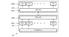
図3Aを参照すると、この発明の実施形態に従って、構成され、動作可能な未処理データ(UPD)ハンドリングユニット(UPDHU)300を描画する概略ブロック図であり、図3Bおよび図3Cは、図3AのUPDHU300のようなUPDHUの2つの異なる実施形態350および380の概略ブロック図である。ここで使用される「未処理データ」という用語は、処理しようとしているデータの大きなストリームに関連し、典型的には、大きな計算容量を必要とし、例えば、仮想的に「リアルタイム」で(すなわち、できるだけ小さい待ち時間で)処理する必要がある、グラフィックデータの高速ストリーム(例えば、4Kビデオカメラから受信された)である。図3Aに描画されるUPDHU300のアーキテクチャは、CPU-GPUの既知のアーキテクチャに典型的な、データストリームの固有のボトルネックを克服するように設計され、データ獲得の入力ストリームは、最初に、CPUにより処理され、次に、一時的にCPUに関連付けられたCPUメモリ、および/またはRAMに記憶され、次に、(例えば、周辺コンポーネント相互接続イクスプレス(PCIe)バスを介して)GPUに再び転送され、GPUの一部である複数のストリーミングプロセッサに送信される前に、GPUプロセッサにより再び処理される。
3A is a schematic block diagram illustrating a raw data (UPD) handling unit (UPDHU) 300 constructed and operable in accordance with an embodiment of the present invention, and FIGS. 3B and 3C are schematic block diagrams of two
図3Aに関して、ここで記載された例は、アドバンスト・イクステンシブル・インタフェース(AXI)に従って、動作するようにプログラムされたフィールドプログラマブルゲートアレイ(FPGA)の使用を示しているが、当業者には、ここに記載した動作の方法は、それぞれのGPUとインタフェースするように適合し、および高いスループットで、グラフィック関連データを大量に転送するのに適した、他のコンピューティングユニットを用いて具現化することができる。 With respect to FIG. 3A, the examples described herein illustrate the use of a field programmable gate array (FPGA) programmed to operate in accordance with an Advanced Extensible Interface (AXI), however, those skilled in the art will appreciate that the methods of operation described herein may be implemented using other computing units adapted to interface with respective GPUs and suitable for transferring large amounts of graphics-related data at high throughput.
この発明の実施形態によれば、データストリーム・デバイダ・ユニット(DSDU)304は、例えば、大量のストリーミングUPD、例えばカメラからのビデオストリームを受信し、それを複数のより小さなストリームに分散し、GPUのSMsに転送するようにプログラムされた、FPGAを用いて具現化することができる。FPGAとGPUは、さらに、GPUの複数のSMsの、少なくとも1つのSMが完全にロードされるやいなや、GPUが、転送されたグラフィックデータの処理を開始するように動作するようにプログラムすることができる。ほとんどの場合、完全にロードされたSMsは、フルデータファイルよりも小さいデータ量を保持し、それゆえ、GPUによる処理は、この実施形態に従って開始され、データファイル全体がGPUにロードされた後で、処理を開始する一般的に知られている実施形態に比べて、はるかに速い。 According to an embodiment of the invention, the data stream divider unit (DSDU) 304 can be embodied, for example, with an FPGA programmed to receive a large amount of streaming UPD, e.g., a video stream from a camera, and distribute it into multiple smaller streams and forward them to the SMs of the GPU. The FPGA and the GPU can be further programmed to operate such that the GPU starts processing the transferred graphic data as soon as at least one of the SMs of the GPU is fully loaded. In most cases, a fully loaded SM holds a smaller amount of data than a full data file, and therefore processing by the GPU is started according to this embodiment much faster than commonly known embodiments that start processing after the entire data file is loaded into the GPU.
一例示実施形態において、UPDHU300は、複数の先入れ先出し(FIFO)レジスタ/ストレージユニットアレイ304A(FIFOユニットは、個別に示されていない)を備えたDSDU304を備え、そのうちの1つのFIFOユニットを、GPU320のSMs318の各々に割当てることができる。いくつかの実施形態において、DSDU304により受信されるUPDストリームは、複数のデータユニットに分割され、FIFOユニット304Aを介して、GPU320に転送することができ、AXIインタフェースのようなインタフェースユニットを介して、GPUにブロードキャストすることができ、それにより、各FIFO304Aのデータユニットが、関連するSM318に転送され、それにより、例えば、シングルアクション・マルチデータ(SEVID)コンピューティングを可能にする。GPU320の各(単一でも)SM318は、AXIインタフェースを介して、関連するFIFO304Aから受信した未処理データのそれぞれの部分がロードされるとき、GPU320は、処理を開始することができ、UPDファイル全体がロードされるまで待つ必要はない。
In one example embodiment, the
MSU310は、長いストリームのグラフィックデータを受信するように構成された、未処理データインタフェースユニット302を備えることができる。インタフェースユニット302を介して受信した大量の未処理データは、より小さなサイズの複数の数のデータユニットに分割され、FIFOユニット304A内の割り当てられたFIFOユニットを介して転送され、次に、AXIチャネル315で、GPU AXIインタフェースを介して、GPU320の割り当てられたSM318に転送される。SMs318のそれぞれのSMにより処理されたデータユニットは、次に、AXI接続を介して、MSUに転送することができる。上記のように、上述した実施形態では、CPU-GPUアーキテクチャにおいて、典型的に大きなオーバヘッドが節約される。
The
図3Bおよび3Cは、この発明の実施形態に従う、図3AのMSU310を具現化する2つのオプションのアーキテクチャの概略ブロック図を描画する。図3Bは、MSU350がFIU356とGPU358を備えることを描画する。FIU356は、複数のFIFOユニット(集合的に356Aと名前が付けられている)-FIFO0、FIFOi・・・FIFOnを備える。各FIFOユニットは、割り当てられたFPGA AXI(F-AXI)ユニット-F-AXI0、F-AXIi・・・F-AXIn(集合的に356Bと名前が付けられている)とアクティブ通信中であり得る。別個のF-AXIユニットの各々は、間接的に、割り当てられたGPU AXI(G-AXI)ユニット-G-AXI0、G-AXIi・・・G-AXInとダイレクトに接続し得る。G-AXIインタフェースユニットの各々は、割り当てられたSM-SM0、SMi・・・SMnとアクティブに接続することができ、データを供給することができる。
3B and 3C depict schematic block diagrams of two optional architectures embodying the
さらに他の実施形態によれば、図3Cに示すように、MSU380は、FIU386とGPU388を備える。FIU386は、複数のFIFOユニット(集合的に386Aの名前がつけられている)-FIFO0、FIFOi・・・FIFOnを備えることができる。各FIFOユニットは、複数のFIFOユニットから単一のAXIストリームへのデータストリームの管理を制御するように構成することが出来るFPGA AXI(F-AXI)ユニットとアクティブに通信することができる。AXIストリームは、GPU388のAXIインタフェースに送信して、次にそれぞれのSMsユニット-SM0、SMi、・・・SMnに分割することができる。図3Bに描画されるアーキテクチャは、より高速な全体性能を提供することができるが、(記載した回路を具現化する集積回路(IC)のために)より多くのピンと、より多くのワイヤ/導管(conduits)を必要とする場合がある。図3Cに描画される、アーキテクチャは、相対的により遅い全体性能を提供するが、(記載した回路を具現化する集積回路(IC)のために)より少ないピンと、より少ないワイヤ/導管(conduits)しか必要としない。
According to yet another embodiment, as shown in FIG. 3C,
上述した、デバイス、構造、および方法は、既知のアーキテクチャおよび方法に比べて、大量の未処理データの処理を加速することができる。例えば、既知の実施形態において、処理/アルゴリズムがHPU上で開始できる前に、画像全体を転送する必要がある。画像サイズが1GBの場合、GPUへデータを転送するPCI-Eバスの理論上のスループットは、32GB/sであり、待ち時間は、1GB/(32GB/s)=1/32s=31.125ms≒31.3msである。それに反して、この発明の実施形態に従うFPGAを用いると、すべてのSMユニットをフルにロードする必要があるだけである。たとえば、Tesla P100 GPUには、56個のSMユニットがあり、各SMには、32ビット(単精度モード)をサポートする64コアまたは64ビット(拡張精度モード)をサポートする32コアがあるため、完全にロードされたGPUのデータサイズ(単精度モードまたは拡張精度モードで同じ結果)は、56*322*64=114688ビット=14.336M Mバイトである。FPGAからGPU AXIストリームへの理論的スループットは、896MB/S(56レーンの場合)であり、待ち時間は、14.336MB(896MB/s)=14.336/896s=16msであり、これは実質半分の待ち時間である。 The above-mentioned devices, structures and methods can accelerate the processing of large amounts of raw data compared to known architectures and methods. For example, in known embodiments, the entire image needs to be transferred before the processing/algorithms can start on the HPU. For an image size of 1 GB, the theoretical throughput of the PCI-E bus transferring data to the GPU is 32 GB/s, and the latency is 1 GB/(32 GB/s) = 1/32 s = 31.125 ms ≈ 31.3 ms. In contrast, with an FPGA according to an embodiment of the present invention, all SM units only need to be fully loaded. For example, a Tesla P100 GPU has 56 SM units, each with 64 cores supporting 32-bit (single precision mode) or 32 cores supporting 64-bit (extended precision mode), so the data size of a fully loaded GPU (same results in single or extended precision mode) is 56*322*64=114688 bits=14.336MB. The theoretical throughput from the FPGA to the GPU AXI stream is 896MB/S (for 56 lanes), and the latency is 14.336MB (896MB/s) = 14.336/896s = 16ms, which is effectively half the latency.
本明細書では、本発明の特定の特徴を例示および説明してきたが、多くの修正、置換、変更、および同等物が当業者に思い浮かぶであろう。したがって、添付の特許請求の範囲は、本発明の真の精神の範囲内に、あるそのようなすべての修正および変更を網羅することを意図していることを理解されたい。 While certain features of the invention have been illustrated and described herein, many modifications, substitutions, changes, and equivalents will occur to those skilled in the art. It is therefore to be understood that the appended claims are intended to cover all such modifications and changes that fall within the true spirit of the invention.
Claims (6)
前記データ部分を受信するように構成された、第1のアドバンスト・イクステンシブル・インタフェース(AXI)ユニットと、
を備えたデータ・ストリーム・デバイダ・ユニット(DSDU)(304)と、
前記第1のAXIユニットからデータ部分を受信するように構成された、第2のアドバンスト・イクステンシブル・インタフェース(AXI)ユニットと、
それぞれのFIFOレジスタから各データ部分を受信するように構成され、前記受信したデータ部分を処理するように構成された、複数のストリーミングマルチプロセッサ(SM)と、
を備えたグラフィックプロセッシングユニット(GPU)と、
を備えた、GPUでの処理がまだ施されていない未処理データを処理する回路。 an array including a plurality of first-in, first-out (FIFO) registers configured to receive a stream of data, divide the stream of data into data portions, and pass each of the data portions through one of a plurality of FIFO registers;
a first Advanced Extensible Interface (AXI) unit configured to receive the data portion;
A data stream divider unit (DSDU) (304) comprising:
a second Advanced Extensible Interface (AXI) unit configured to receive data portions from the first AXI unit; and
a plurality of streaming multiprocessors (SMs) configured to receive respective data portions from respective FIFO registers and configured to process said received data portions;
A graphic processing unit (GPU) having
A circuit for processing raw data that has not yet been processed by a GPU , comprising:
前記ストリームを複数のデータ部分に分割するステップと、
データストリームデバイダユニット(DSDU)の特定のFIFOレジスタを介して各データ部分を通過させるステップと、
前記特定のFIFOレジスタからのデータ部分を、処理のためにグラフィックプロセッサユニット(GPU)内の、前記特定のFIFOレジスタに割り当てられたストリーミングマルチプロセッサ(SM)に転送するステップと、
を備え、
前記データ部分は、前記DSDU内の、第1のアドバンスト・イクステンシブル・インタフェース(AXI)ユニットと、前記GPU内の、第2のアドバンスト・イクステンシブル・インタフェース(AXI)ユニットを介して転送される、
大容量のデータを効率的に処理する方法。 receiving a stream of raw data that has not yet been processed by a graphics processor unit (GPU) ;
dividing the stream into a number of data portions;
passing each data portion through a specific FIFO register of a data stream divider unit (DSDU);
transferring the data portion from the particular FIFO register to a streaming multiprocessor (SM) in a graphics processor unit (GPU) assigned to the particular FIFO register for processing;
Equipped with
the data portion is transferred via a first Advanced Extensible Interface (AXI) unit in the DSDU and a second Advanced Extensible Interface (AXI) unit in the GPU;
How to process large amounts of data efficiently.
Applications Claiming Priority (4)
| Application Number | Priority Date | Filing Date | Title |
|---|---|---|---|
| US201762552475P | 2017-08-31 | 2017-08-31 | |
| US62/552,475 | 2017-08-31 | ||
| JP2020512508A JP2020532795A (en) | 2017-08-31 | 2018-08-30 | Systems and methods for high throughput in multiple computations |
| PCT/IL2018/050965 WO2019043710A1 (en) | 2017-08-31 | 2018-08-30 | System and method for high throughput in multiple computations |
Related Parent Applications (1)
| Application Number | Title | Priority Date | Filing Date |
|---|---|---|---|
| JP2020512508A Division JP2020532795A (en) | 2017-08-31 | 2018-08-30 | Systems and methods for high throughput in multiple computations |
Publications (2)
| Publication Number | Publication Date |
|---|---|
| JP2023078204A JP2023078204A (en) | 2023-06-06 |
| JP7547526B2 true JP7547526B2 (en) | 2024-09-09 |
Family
ID=65527276
Family Applications (2)
| Application Number | Title | Priority Date | Filing Date |
|---|---|---|---|
| JP2020512508A Pending JP2020532795A (en) | 2017-08-31 | 2018-08-30 | Systems and methods for high throughput in multiple computations |
| JP2023033382A Active JP7547526B2 (en) | 2017-08-31 | 2023-03-06 | Systems and methods for high throughput in multiple computations - Patents.com |
Family Applications Before (1)
| Application Number | Title | Priority Date | Filing Date |
|---|---|---|---|
| JP2020512508A Pending JP2020532795A (en) | 2017-08-31 | 2018-08-30 | Systems and methods for high throughput in multiple computations |
Country Status (4)
| Country | Link |
|---|---|
| US (2) | US10942746B2 (en) |
| EP (1) | EP3676710B1 (en) |
| JP (2) | JP2020532795A (en) |
| WO (1) | WO2019043710A1 (en) |
Families Citing this family (2)
| Publication number | Priority date | Publication date | Assignee | Title |
|---|---|---|---|---|
| US11204819B2 (en) | 2018-12-21 | 2021-12-21 | Samsung Electronics Co., Ltd. | System and method for offloading application functions to a device |
| US20220147320A1 (en) * | 2020-11-09 | 2022-05-12 | Vizzio Technologies Pte Ltd | Highly parallel processing system |
Citations (5)
| Publication number | Priority date | Publication date | Assignee | Title |
|---|---|---|---|---|
| JP2003502958A (en) | 1999-06-23 | 2003-01-21 | ジェネラル・インスツルメント・コーポレイション | Execution architecture of a multi-channel MPEG video transcoder using multiple programmable processors |
| JP2006091982A (en) | 2004-09-21 | 2006-04-06 | Canon Inc | On-chip bus system |
| JP2012146323A (en) | 2007-11-30 | 2012-08-02 | Imagination Technologies Ltd | Multi-core geometry processing in tile based rendering system |
| JP2012150735A (en) | 2011-01-21 | 2012-08-09 | Sony Corp | Interconnect equipment |
| JP2015156645A (en) | 2014-02-20 | 2015-08-27 | 三星電子株式会社Samsung Electronics Co.,Ltd. | System on chip, bus interface circuit, and bus interface method |
Family Cites Families (17)
| Publication number | Priority date | Publication date | Assignee | Title |
|---|---|---|---|---|
| JPH0258153A (en) * | 1988-08-24 | 1990-02-27 | Mitsubishi Electric Corp | information processing equipment |
| JPH06324997A (en) * | 1993-05-10 | 1994-11-25 | Nippon Steel Corp | FIFO storage device incorporating a plurality of FIFO memories |
| JP2001134490A (en) * | 1999-11-01 | 2001-05-18 | Fujitsu Ltd | Cache memory control method and computer realizing the method |
| JP4043225B2 (en) * | 2001-12-10 | 2008-02-06 | 株式会社ルネサステクノロジ | Cache apparatus and method |
| CN101849227A (en) | 2005-01-25 | 2010-09-29 | 透明信息技术有限公司 | Graphics processing and display system employing multiple graphics cores on a silicon chip of monolithic construction |
| JP4904802B2 (en) * | 2005-02-01 | 2012-03-28 | セイコーエプソン株式会社 | Cache memory and processor |
| JP4837305B2 (en) * | 2005-05-10 | 2011-12-14 | ルネサスエレクトロニクス株式会社 | Microprocessor and control method of microprocessor |
| US8400458B2 (en) * | 2009-09-09 | 2013-03-19 | Hewlett-Packard Development Company, L.P. | Method and system for blocking data on a GPU |
| US9639479B2 (en) * | 2009-09-23 | 2017-05-02 | Nvidia Corporation | Instructions for managing a parallel cache hierarchy |
| JP5487882B2 (en) * | 2009-10-27 | 2014-05-14 | セイコーエプソン株式会社 | Image processing apparatus and image processing method |
| JP5648465B2 (en) * | 2010-12-17 | 2015-01-07 | 富士通セミコンダクター株式会社 | Graphics processor |
| US9092267B2 (en) * | 2011-06-20 | 2015-07-28 | Qualcomm Incorporated | Memory sharing in graphics processing unit |
| US8954599B2 (en) * | 2011-10-28 | 2015-02-10 | Hewlett-Packard Development Company, L.P. | Data stream operations |
| EP2795472A1 (en) | 2011-12-23 | 2014-10-29 | Intel Corporation | Methods and apparatus for efficient communication between caches in hierarchical caching design |
| US9720829B2 (en) | 2011-12-29 | 2017-08-01 | Intel Corporation | Online learning based algorithms to increase retention and reuse of GPU-generated dynamic surfaces in outer-level caches |
| US9244683B2 (en) * | 2013-02-26 | 2016-01-26 | Nvidia Corporation | System, method, and computer program product for implementing large integer operations on a graphics processing unit |
| US9086813B2 (en) * | 2013-03-15 | 2015-07-21 | Qualcomm Incorporated | Method and apparatus to save and restore system memory management unit (MMU) contexts |
-
2018
- 2018-08-30 JP JP2020512508A patent/JP2020532795A/en active Pending
- 2018-08-30 WO PCT/IL2018/050965 patent/WO2019043710A1/en not_active Ceased
- 2018-08-30 US US16/642,026 patent/US10942746B2/en active Active
- 2018-08-30 EP EP18850323.9A patent/EP3676710B1/en active Active
-
2021
- 2021-02-03 US US17/167,077 patent/US20210191729A1/en not_active Abandoned
-
2023
- 2023-03-06 JP JP2023033382A patent/JP7547526B2/en active Active
Patent Citations (5)
| Publication number | Priority date | Publication date | Assignee | Title |
|---|---|---|---|---|
| JP2003502958A (en) | 1999-06-23 | 2003-01-21 | ジェネラル・インスツルメント・コーポレイション | Execution architecture of a multi-channel MPEG video transcoder using multiple programmable processors |
| JP2006091982A (en) | 2004-09-21 | 2006-04-06 | Canon Inc | On-chip bus system |
| JP2012146323A (en) | 2007-11-30 | 2012-08-02 | Imagination Technologies Ltd | Multi-core geometry processing in tile based rendering system |
| JP2012150735A (en) | 2011-01-21 | 2012-08-09 | Sony Corp | Interconnect equipment |
| JP2015156645A (en) | 2014-02-20 | 2015-08-27 | 三星電子株式会社Samsung Electronics Co.,Ltd. | System on chip, bus interface circuit, and bus interface method |
Also Published As
| Publication number | Publication date |
|---|---|
| US20200183698A1 (en) | 2020-06-11 |
| JP2020532795A (en) | 2020-11-12 |
| US20210191729A1 (en) | 2021-06-24 |
| EP3676710A1 (en) | 2020-07-08 |
| JP2023078204A (en) | 2023-06-06 |
| WO2019043710A1 (en) | 2019-03-07 |
| EP3676710A4 (en) | 2021-07-28 |
| EP3676710C0 (en) | 2025-05-14 |
| US10942746B2 (en) | 2021-03-09 |
| EP3676710B1 (en) | 2025-05-14 |
Similar Documents
| Publication | Publication Date | Title |
|---|---|---|
| US11768601B2 (en) | System and method for accelerated data processing in SSDS | |
| US11625807B2 (en) | Low power and low latency GPU coprocessor for persistent computing | |
| US9075764B2 (en) | Multiprocessor system-on-a-chip for machine vision algorithms | |
| CN103221935B (en) | The method and apparatus moving data to general-purpose register file from simd register file | |
| KR101661720B1 (en) | A processing unit with a plurality of shader engines | |
| US9164690B2 (en) | System, method, and computer program product for copying data between memory locations | |
| JP7547526B2 (en) | Systems and methods for high throughput in multiple computations - Patents.com | |
| US20140115195A1 (en) | Dma vector buffer | |
| US10838868B2 (en) | Programmable data delivery by load and store agents on a processing chip interfacing with on-chip memory components and directing data to external memory components | |
| DE112020006536T5 (en) | Advanced memory communication | |
| EP4634787A1 (en) | Fused data generation and associated communication | |
| US20200387444A1 (en) | Extended memory interface | |
| Jeong et al. | Performance of Kepler GTX Titan GPUs and Xeon Phi System | |
| CN106201931B (en) | A kind of hypervelocity matrix operation coprocessor system | |
| JP2010272066A (en) | Heterogeneous multi-core processor | |
| US9824413B2 (en) | Sort-free threading model for a multi-threaded graphics pipeline | |
| US20240069965A1 (en) | Systems and methods for executing compute functions | |
| CN104615557A (en) | Multi-core fine grit synchronous DMA transmission method used for GPDSP | |
| US20180095877A1 (en) | Processing scattered data using an address buffer |
Legal Events
| Date | Code | Title | Description |
|---|---|---|---|
| A521 | Request for written amendment filed |
Free format text: JAPANESE INTERMEDIATE CODE: A523 Effective date: 20230315 |
|
| A621 | Written request for application examination |
Free format text: JAPANESE INTERMEDIATE CODE: A621 Effective date: 20230315 |
|
| A977 | Report on retrieval |
Free format text: JAPANESE INTERMEDIATE CODE: A971007 Effective date: 20240229 |
|
| A131 | Notification of reasons for refusal |
Free format text: JAPANESE INTERMEDIATE CODE: A131 Effective date: 20240326 |
|
| A521 | Request for written amendment filed |
Free format text: JAPANESE INTERMEDIATE CODE: A523 Effective date: 20240618 |
|
| TRDD | Decision of grant or rejection written | ||
| A01 | Written decision to grant a patent or to grant a registration (utility model) |
Free format text: JAPANESE INTERMEDIATE CODE: A01 Effective date: 20240730 |
|
| A61 | First payment of annual fees (during grant procedure) |
Free format text: JAPANESE INTERMEDIATE CODE: A61 Effective date: 20240828 |
|
| R150 | Certificate of patent or registration of utility model |
Ref document number: 7547526 Country of ref document: JP Free format text: JAPANESE INTERMEDIATE CODE: R150 |