JP7540407B2 - Laser emitting device and optical distance measuring device - Google Patents
Laser emitting device and optical distance measuring device Download PDFInfo
- Publication number
- JP7540407B2 JP7540407B2 JP2021140693A JP2021140693A JP7540407B2 JP 7540407 B2 JP7540407 B2 JP 7540407B2 JP 2021140693 A JP2021140693 A JP 2021140693A JP 2021140693 A JP2021140693 A JP 2021140693A JP 7540407 B2 JP7540407 B2 JP 7540407B2
- Authority
- JP
- Japan
- Prior art keywords
- switch
- diode
- laser
- power supply
- boost
- Prior art date
- Legal status (The legal status is an assumption and is not a legal conclusion. Google has not performed a legal analysis and makes no representation as to the accuracy of the status listed.)
- Active
Links
Images


Classifications
-
- G—PHYSICS
- G01—MEASURING; TESTING
- G01S—RADIO DIRECTION-FINDING; RADIO NAVIGATION; DETERMINING DISTANCE OR VELOCITY BY USE OF RADIO WAVES; LOCATING OR PRESENCE-DETECTING BY USE OF THE REFLECTION OR RERADIATION OF RADIO WAVES; ANALOGOUS ARRANGEMENTS USING OTHER WAVES
- G01S7/00—Details of systems according to groups G01S13/00, G01S15/00, G01S17/00
- G01S7/48—Details of systems according to groups G01S13/00, G01S15/00, G01S17/00 of systems according to group G01S17/00
- G01S7/483—Details of pulse systems
- G01S7/484—Transmitters
-
- G—PHYSICS
- G01—MEASURING; TESTING
- G01S—RADIO DIRECTION-FINDING; RADIO NAVIGATION; DETERMINING DISTANCE OR VELOCITY BY USE OF RADIO WAVES; LOCATING OR PRESENCE-DETECTING BY USE OF THE REFLECTION OR RERADIATION OF RADIO WAVES; ANALOGOUS ARRANGEMENTS USING OTHER WAVES
- G01S17/00—Systems using the reflection or reradiation of electromagnetic waves other than radio waves, e.g. lidar systems
- G01S17/02—Systems using the reflection of electromagnetic waves other than radio waves
- G01S17/06—Systems determining position data of a target
- G01S17/08—Systems determining position data of a target for measuring distance only
- G01S17/10—Systems determining position data of a target for measuring distance only using transmission of interrupted, pulse-modulated waves
-
- H—ELECTRICITY
- H01—ELECTRIC ELEMENTS
- H01S—DEVICES USING THE PROCESS OF LIGHT AMPLIFICATION BY STIMULATED EMISSION OF RADIATION [LASER] TO AMPLIFY OR GENERATE LIGHT; DEVICES USING STIMULATED EMISSION OF ELECTROMAGNETIC RADIATION IN WAVE RANGES OTHER THAN OPTICAL
- H01S5/00—Semiconductor lasers
- H01S5/04—Processes or apparatus for excitation, e.g. pumping, e.g. by electron beams
- H01S5/042—Electrical excitation ; Circuits therefor
- H01S5/0428—Electrical excitation ; Circuits therefor for applying pulses to the laser
-
- H—ELECTRICITY
- H02—GENERATION; CONVERSION OR DISTRIBUTION OF ELECTRIC POWER
- H02M—APPARATUS FOR CONVERSION BETWEEN AC AND AC, BETWEEN AC AND DC, OR BETWEEN DC AND DC, AND FOR USE WITH MAINS OR SIMILAR POWER SUPPLY SYSTEMS; CONVERSION OF DC OR AC INPUT POWER INTO SURGE OUTPUT POWER; CONTROL OR REGULATION THEREOF
- H02M3/00—Conversion of DC power input into DC power output
- H02M3/02—Conversion of DC power input into DC power output without intermediate conversion into AC
- H02M3/04—Conversion of DC power input into DC power output without intermediate conversion into AC by static converters
- H02M3/10—Conversion of DC power input into DC power output without intermediate conversion into AC by static converters using discharge tubes with control electrode or semiconductor devices with control electrode
- H02M3/145—Conversion of DC power input into DC power output without intermediate conversion into AC by static converters using discharge tubes with control electrode or semiconductor devices with control electrode using devices of a triode or transistor type requiring continuous application of a control signal
- H02M3/155—Conversion of DC power input into DC power output without intermediate conversion into AC by static converters using discharge tubes with control electrode or semiconductor devices with control electrode using devices of a triode or transistor type requiring continuous application of a control signal using semiconductor devices only
- H02M3/156—Conversion of DC power input into DC power output without intermediate conversion into AC by static converters using discharge tubes with control electrode or semiconductor devices with control electrode using devices of a triode or transistor type requiring continuous application of a control signal using semiconductor devices only with automatic control of output voltage or current, e.g. switching regulators
- H02M3/158—Conversion of DC power input into DC power output without intermediate conversion into AC by static converters using discharge tubes with control electrode or semiconductor devices with control electrode using devices of a triode or transistor type requiring continuous application of a control signal using semiconductor devices only with automatic control of output voltage or current, e.g. switching regulators including plural semiconductor devices as final control devices for a single load
- H02M3/1584—Conversion of DC power input into DC power output without intermediate conversion into AC by static converters using discharge tubes with control electrode or semiconductor devices with control electrode using devices of a triode or transistor type requiring continuous application of a control signal using semiconductor devices only with automatic control of output voltage or current, e.g. switching regulators including plural semiconductor devices as final control devices for a single load with a plurality of power processing stages connected in parallel
-
- H—ELECTRICITY
- H10—SEMICONDUCTOR DEVICES; ELECTRIC SOLID-STATE DEVICES NOT OTHERWISE PROVIDED FOR
- H10H—INORGANIC LIGHT-EMITTING SEMICONDUCTOR DEVICES HAVING POTENTIAL BARRIERS
- H10H20/00—Individual inorganic light-emitting semiconductor devices having potential barriers, e.g. light-emitting diodes [LED]
- H10H20/80—Constructional details
Landscapes
- Physics & Mathematics (AREA)
- Engineering & Computer Science (AREA)
- General Physics & Mathematics (AREA)
- Electromagnetism (AREA)
- Computer Networks & Wireless Communication (AREA)
- Radar, Positioning & Navigation (AREA)
- Remote Sensing (AREA)
- Power Engineering (AREA)
- Condensed Matter Physics & Semiconductors (AREA)
- Optics & Photonics (AREA)
- Semiconductor Lasers (AREA)
- Optical Radar Systems And Details Thereof (AREA)
Description
本開示は、レーザ発光装置および光測距装置に関する。 This disclosure relates to a laser emitting device and an optical distance measuring device.
レーザ光を対象物に向けて照射して、対象物からの反射光を受光し、照射から受光までの時間を計測することで、対象物までの距離を測定する測距装置が知られている。測距性能を向上させるためには、高出力のレーザ光を照射することが求められる。そして、高出力のレーザ光を照射させるためには、レーザ光を発光するレーザダイオードに高い電圧を印加する必要がある。レーザダイオードに高い電圧を印加するために、昇圧回路を用いることが考えられる。特許文献1には、チョッパ昇圧回路を備えるレーザ発光装置が記載されている。
Distance measuring devices are known that measure the distance to an object by irradiating the object with laser light, receiving the reflected light from the object, and measuring the time between irradiation and reception. In order to improve distance measuring performance, it is necessary to irradiate a high-power laser light. And to irradiate a high-power laser light, it is necessary to apply a high voltage to the laser diode that emits the laser light. In order to apply a high voltage to the laser diode, it is possible to use a boost circuit.
レーザダイオードに短時間で大電流を流すと、配線の寄生インダクタンスにより、レーザダイオードが目標とする発光の後に、意図せず発光する場合がある。チョッパ昇圧回路が有するコイルの通電・非通電を切り替えるためのスイッチ用トランジスタのボディダイオードにより、レーザダイオードに電流が流れる経路が形成されるためである。レーザダイオードが意図せず発光すると測距精度が低下するおそれがある。 When a large current is passed through a laser diode in a short period of time, the parasitic inductance of the wiring can cause the laser diode to emit light unintentionally after the intended light emission. This is because the body diode of the switching transistor, which switches the coil in the chopper boost circuit between energized and de-energized, forms a path through which current flows through the laser diode. If the laser diode emits light unintentionally, there is a risk of reduced distance measurement accuracy.
本開示は、以下の形態として実現することが可能である。 This disclosure can be realized in the following forms:
本開示の第1の形態によれば、レーザ発光装置(10)が提供される。このレーザ発光装置は、直流電源(V1)により供給される直流電圧を昇圧する昇圧回路(11)であって、コイル(L1)と第1ダイオード(D1)とが直列に接続された第1直列接続体(DC1)と、前記コイルの通電・非通電を切り替えるための第1スイッチ(Q1)と、コンデンサ(C1)と、を有する昇圧回路と、前記昇圧回路により昇圧された電圧が供給されるレーザダイオード(LD)と、前記レーザダイオードの通電・非通電を切り替えるための第2スイッチ(Q2)と、を有する駆動回路(12)と、前記第1スイッチと直列に接続される第2ダイオード(D2)であって、前記直流電源に対して順方向接続される第2ダイオードと、前記昇圧回路と前記駆動回路とを制御する発光駆動部(13)と、を備え、前記第1直列接続体の一端は前記直流電源の正極に接続されており、前記第1ダイオードは前記直流電源に対して順方向接続されており、前記第1直列接続体の他端と、前記直流電源の負極との間に、前記第1スイッチと前記第2ダイオードとが接続されている。 According to a first aspect of the present disclosure, there is provided a laser light emitting device (10). This laser light emitting device includes a boost circuit (11) for boosting a DC voltage supplied by a DC power supply (V1), the boost circuit having a first series connection (DC1) in which a coil (L1) and a first diode (D1) are connected in series, a first switch (Q1) for switching the coil between energized and de-energized, and a capacitor (C1), a laser diode (LD) to which the voltage boosted by the boost circuit is supplied, and a second switch (Q2) for switching the laser diode between energized and de-energized. the first switch is connected in series to the positive electrode of the DC power supply , and the first diode is connected in a forward direction to the DC power supply; and a light-emitting drive unit (13) that controls the boost circuit and the drive circuit , one end of the first series-connected body is connected to the positive electrode of the DC power supply, the first diode is connected in a forward direction to the DC power supply, and the first switch and the second diode are connected between the other end of the first series-connected body and the negative electrode of the DC power supply.
この形態のレーザ発光装置によれば、レーザ発光装置において、配線の寄生インダクタンスにより発生する、目標の発光の後に、意図せず発光する場合の電流経路の電流の流れる向きに対して、第2ダイオードは、逆方向に接続されている。このため、第2ダイオードにより、電流経路における電流の流れは遮られるため、レーザダイオードの意図しない発光を抑制することができる。よって、測距精度の低下を抑制することができる。 In this form of laser emission device, the second diode is connected in the opposite direction to the direction of current flow in the current path in the case of unintentional emission after target emission, which occurs due to parasitic inductance in the wiring. Therefore, the second diode blocks the current flow in the current path, making it possible to suppress unintentional emission of the laser diode. This makes it possible to suppress a decrease in distance measurement accuracy.
本開示の第2の形態によれば、光測距装置(100)が提供される。この光測距装置は、直流電源(V1)により供給される直流電圧を昇圧する昇圧回路(11)であって、コイル(L1)と第1ダイオード(D1)とが直列に接続された第1直列接続体(DC1)と、前記コイルの通電・非通電を切り替えるための第1スイッチ(Q1)と、コンデンサ(C1)と、を有する昇圧回路と、前記昇圧回路により昇圧された電圧が供給されるレーザダイオード(LD)と、前記レーザダイオードの通電・非通電を切り替えるための第2スイッチ(Q2)と、を有する駆動回路(12)と、前記第1スイッチと直列に接続される第2ダイオード(D2)であって、前記直流電源に対して順方向接続される第2ダイオードと、前記昇圧回路と前記駆動回路とを制御する発光駆動部(13)と、を備え、前記第1直列接続体の一端は前記直流電源の正極に接続されており、前記第1ダイオードは前記直流電源に対して順方向接続されており、前記第1直列接続体の他端と、前記直流電源の負極との間に、前記第1スイッチと前記第2ダイオードとが接続されている、レーザ発光装置(10)と、前記レーザダイオードから発光されたレーザ光(IL)が対象物(OB)により反射された反射光(RL)を受光する受光部(30)と、前記レーザ光が発光されてから前記反射光が受光されるまでの時間を用いて前記対象物までの距離を算出する算出部(62)と、を備える。 According to a second aspect of the present disclosure, there is provided an optical distance measuring device (100). The optical distance measuring device includes a boost circuit (11) for boosting a DC voltage supplied by a DC power source (V1), the boost circuit having a first series connection (DC1) in which a coil (L1) and a first diode (D1) are connected in series, a first switch (Q1) for switching the coil between energized and de-energized, and a capacitor (C1), a laser diode (LD) to which the voltage boosted by the boost circuit is supplied, and a drive circuit (12) having a second switch (Q2) for switching the laser diode between energized and de-energized, and a second diode (D2) connected in series with the first switch and forward-connected to the DC power source. a light emission driving unit (13) that controls the boost circuit and the driving circuit , one end of the first series connection being connected to the positive electrode of the DC power supply, the first diode being forward connected to the DC power supply, and the first switch and the second diode being connected between the other end of the first series connection and the negative electrode of the DC power supply; a light receiving unit (30) that receives reflected light (RL) of laser light (IL) emitted from the laser diode and reflected by an object (OB); and a calculation unit (62) that calculates the distance to the object using the time from when the laser light is emitted to when the reflected light is received.
この形態の光測距装置によれば、レーザダイオードの意図しない発光が抑制されたレーザ発光装置を用いることにより、測距精度が向上した光測距装置を提供することができる。 With this type of optical distance measuring device, it is possible to provide an optical distance measuring device with improved distance measuring accuracy by using a laser emitting device that suppresses unintended emission of light from the laser diode.
A.第1実施形態:
A1.光測距装置の構成:
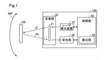
図1に示す光測距装置100は、レーザ光ILを発光し、対象物OBによって反射された反射光RLを受光することによって、対象物OBまでの距離を検出する。光測距装置100は、例えば、車両に搭載されて用いられる。本実施形態において、光測距装置100は、LiDAR(Light Detection And Ranging)である。光測距装置100は、レーザ発光装置10と、走査部20と、受光部30と、制御部60とを備える。レーザ発光装置10は、測距のためのレーザ光ILを発光する。
A. First embodiment:
A1. Configuration of the optical distance measuring device:
The optical
制御部60は、CPUおよびメモリを備えるコンピュータとして構成されている。制御部60は、レーザ発光装置10と、走査部20と、受光部30との動作を制御する。制御部60は、さらに、算出部62を備える。算出部62は、対象物OBまでの距離を算出する。算出部62は、メモリに記憶されたプログラムをCPUが実行することにより実現されてもよく、電子回路により実現されてもよい。
The
レーザ発光装置10は、パルス状のレーザ光ILを発光する後述のレーザダイオードLDを備える。レーザダイオードLDから発せられたレーザ光ILは、図示しないコリメートレンズにより平行光にされ、走査部20に入る。
The
走査部20は、予め定められた測定範囲MR内でレーザ光ILを走査する。走査部20は、レーザ光ILを反射するミラー21と、ミラー21を駆動する図示しないロータリソレノイドとを備える。ロータリソレノイドが、予め定められた角度範囲内で正転および逆転を繰り返すことにより、レーザ光ILは、測定範囲MR内で走査される。
The
受光部30は、レーザダイオードLDから発光されたレーザ光ILが対象物OBにより反射された反射光RLを受光する。受光部30は、受光した光の強度に応じた検出信号を算出部62に出力する。
The light
算出部62は、受光部30から入力された検出信号を用いて、対象物OBまでの距離を算出する。具体的には、算出部62は、レーザ光ILが発光されてから反射光RLが受光されるまでの時間である飛行時間(TOF:Time of Flight)を用いて、対象物OBまでの距離を算出する。
The
A2.レーザ発光装置の回路構成:
図2に示すように、レーザ発光装置10は、直流電源V1と、昇圧回路11と、駆動回路12と、第2ダイオードD2と、発光駆動部13とを有する。昇圧回路11は、直流電源V1により供給される直流電圧を昇圧する。昇圧回路11は、コイルL1と、第1ダイオードD1と、第1スイッチQ1と、コンデンサC1とを有する。第1スイッチQ1は、コイルL1の通電・非通電を切り替える。第1ダイオードD1は、直流電源V1に対して順方向接続されている。本実施形態では、コイルL1と第1ダイオードD1とが直列に接続されて、第1直列接続体DC1を構成している。本実施形態では、コイルL1および第1ダイオードD1は、直流電源V1の正極から負極に向かってコイルL1、第1ダイオードD1の順に接続されている。第1直列接続体DC1の一端は、直流電源V1の正極に接続されている。第1直列接続体DC1の他端と、直流電源V1の負極との間に、コンデンサC1が接続されている。
A2. Circuit configuration of the laser emitting device:
As shown in FIG. 2, the laser
第2ダイオードD2は、第1スイッチQ1と直列に接続されると共に、直流電源V1に対して順方向接続されている。本実施形態では、第2ダイオードD2と、第1スイッチQ1とが直列に接続された接続体が、コンデンサC1に並列接続されている。つまり、第1直列接続体DC1の他端と、直流電源V1の負極との間に、第2ダイオードD2と第1スイッチQ1とが接続されている。本実施形態では、第2ダイオードD2および第1スイッチQ1は、直流電源V1の正極から負極に向かって、第2ダイオードD2、第1スイッチQ1の順に接続されている。 The second diode D2 is connected in series with the first switch Q1 and is connected in the forward direction to the DC power source V1. In this embodiment, the connection in which the second diode D2 and the first switch Q1 are connected in series is connected in parallel to the capacitor C1. In other words, the second diode D2 and the first switch Q1 are connected between the other end of the first series connection DC1 and the negative electrode of the DC power source V1. In this embodiment, the second diode D2 and the first switch Q1 are connected in this order from the positive electrode to the negative electrode of the DC power source V1.
駆動回路12は、昇圧回路11により昇圧された電圧が供給されるレーザダイオードLDと、レーザダイオードLDの通電・非通電を切り替えるための第2スイッチQ2とを有する。具体的には、レーザダイオードLDと、第2スイッチQ2とが直列に接続された接続体が、コンデンサC1に並列接続されている。本実施形態では、第2スイッチQ2およびレーザダイオードLDは、直流電源V1の正極から負極に向かって第2スイッチQ2、レーザダイオードLDの順に接続されている。直流電源V1の負極は、グランドに接続されている。発光駆動部13は、電子回路により実現されており、昇圧回路11と駆動回路12とを制御する。
The
本実施形態において、第2スイッチQ2および第1スイッチQ1は、NチャネルIGFET(Insulated Gate Field Effect Transistor)である。第1スイッチQ1のゲートには、発光駆動部13から出力される第1ゲート信号SG1が入力される。第2スイッチQ2のゲートには、発光駆動部13から出力される第2ゲート信号SG2が入力される。
In this embodiment, the second switch Q2 and the first switch Q1 are N-channel IGFETs (Insulated Gate Field Effect Transistors). The first gate signal SG1 output from the light
後述するように、第1スイッチQ1により、コイルL1の導通・非導通が切り替えられることにより、コンデンサC1の電圧であるコンデンサ電圧VCは、直流電源V1の直流電圧よりも高くなる。そして、第2スイッチQ2がオン状態となることにより、コンデンサC1に蓄積された電荷がレーザダイオードLDに供給され、レーザダイオードLDは発光する。 As described below, the first switch Q1 switches the coil L1 between conductive and non-conductive states, so that the capacitor voltage VC of the capacitor C1 becomes higher than the DC voltage of the DC power supply V1. Then, when the second switch Q2 is turned on, the charge stored in the capacitor C1 is supplied to the laser diode LD, causing the laser diode LD to emit light.
他の実施形態として、コイルL1および第1ダイオードD1は、直流電源V1の正極から負極に向かって第1ダイオードD1、コイルL1の順に接続されてもよい。第2スイッチQ2およびレーザダイオードLDは、直流電源V1の正極から負極に向かってレーザダイオードLD、第2スイッチQ2の順に接続されてもよい。第2ダイオードD2および第1スイッチQ1は、直流電源V1の正極から負極に向かって、第1スイッチQ1、第2ダイオードD2の順に接続されてもよい。第2スイッチQ2および第1スイッチQ1は、IGFET以外のFET(Field Effect Transistor)でもよい。IGFET以外のFETとして、例えば、窒化ガリウム(GaN)を用いたHEMT(High Electron Mobility Transistor)を挙げることができる。なお、HEMTは、HFET(Heterostructure Field-Effect Transistor)とも呼ばれる。さらに、第1スイッチQ1および第2スイッチQ2は、バイポーラトランジスタでもよく、集積回路により構成されてもよい。第1スイッチQ1および第2スイッチQ2は、PチャネルIGFETでもよい。なお、第1スイッチQ1がPチャネルIGFETの場合、第2ダイオードD2および第1スイッチQ1は、直流電源V1の正極から負極に向かって、第1スイッチQ1、第2ダイオードD2の順に接続するとよい。 In another embodiment, the coil L1 and the first diode D1 may be connected in the order of the first diode D1 and the coil L1 from the positive electrode to the negative electrode of the DC power supply V1. The second switch Q2 and the laser diode LD may be connected in the order of the laser diode LD and the second switch Q2 from the positive electrode to the negative electrode of the DC power supply V1. The second diode D2 and the first switch Q1 may be connected in the order of the first switch Q1 and the second diode D2 from the positive electrode to the negative electrode of the DC power supply V1. The second switch Q2 and the first switch Q1 may be FETs (Field Effect Transistors) other than IGFETs. As an example of an FET other than IGFETs, a HEMT (High Electron Mobility Transistor) using gallium nitride (GaN) can be mentioned. The HEMT is also called an HFET (Heterostructure Field-Effect Transistor). Furthermore, the first switch Q1 and the second switch Q2 may be bipolar transistors or may be configured by an integrated circuit. The first switch Q1 and the second switch Q2 may be P-channel IGFETs. When the first switch Q1 is a P-channel IGFET, the second diode D2 and the first switch Q1 should be connected in the order of the first switch Q1 and the second diode D2 from the positive electrode to the negative electrode of the DC power supply V1.
図3に示すように、レーザ発光装置10の各素子を接続する配線には、寄生インダクタンスLpがある。また、第2スイッチQ2および第1スイッチQ1は、IGFETであるためボディダイオードDbが形成されている。このため、レーザ発光装置10が第2ダイオードD2を有さない場合には、レーザダイオードLD、第1スイッチQ1のボディダイオードDb、オン状態の第2スイッチQ2を通る電流経路CPが形成される。したがって、レーザダイオードLDを発光させるために第2スイッチQ2がオン状態となった後、コンデンサC1に蓄積されていた電荷が無くなるのに伴い、レーザダイオードLDを通る電流の流れが無くなると、急激な電流変化に伴い、寄生インダクタンスLpの電磁誘導により、電流経路CPに電流が流れる。電流経路CPに電流が流れると、目標の発光の後に、意図しない発光が行われる。目標の発光を1次発光とも呼ぶのに対して、この意図しない発光を2次発光とも呼ぶ。2次発光は、1次発光に対してレーザダイオードLDに流れる電流は小さい。そこで、本実施形態では、電流経路CPに、レーザダイオードLDが発光する電流の流れとは逆向きに第2ダイオードD2が挿入されている。これにより、2次発光を抑制することができる。なお、2次発光を抑制するために、電流経路CPにダンピング抵抗を挿入する方法も考えられる。しかし、この場合、昇圧動作において流れる電流が大きいため、以下の課題が生じ得る。例えば、ダンピング抵抗による発熱が課題となる。電流値に応じて、複数のダンピング抵抗を配置する必要が生じ、体格が大きくなってしまう点が課題となる。ダンピング抵抗が焼損した場合には、キックバックにより第1スイッチQ1が波及故障する課題がある。この点、本実施形態によれば、ダンピング抵抗を挿入することによる課題を回避することができる。
As shown in FIG. 3, the wiring connecting each element of the laser
A3.レーザ発光装置の駆動方法:
発光駆動部13は、制御部60が行う対象物OBまでの距離を測定する測距処理に合わせて、図4に示す発光処理を行う。発光駆動部13は、第1ステップS1にて、第2スイッチQ2に、駆動オフ信号SDFを出力している期間に、第1スイッチQ1に第1昇圧オン信号SBN1を出力した後、第1スイッチQ1に第1昇圧オフ信号SBF1を出力する。
A3. Method for driving a laser emitting device:
4 in accordance with the distance measurement process for measuring the distance to the object OB performed by the
第1ステップS1では、具体的には、第2スイッチQ2のゲートには、時刻t1から時刻t3まで、駆動オフ信号SDFとしてのロウレベルLの第1ゲート信号SG1が入力される。そして、第1スイッチQ1のゲートには、時刻t1から時刻t2まで、第1昇圧オン信号SBN1としてのハイレベルHの第2ゲート信号SG2が入力された後、時刻t2から時刻t3まで、第1昇圧オフ信号SBF1としてのロウレベルLの第2ゲート信号SG2が入力される。 In the first step S1, specifically, the first gate signal SG1 of low level L as the drive-off signal SDF is input to the gate of the second switch Q2 from time t1 to time t3. Then, the second gate signal SG2 of high level H as the first boost-on signal SBN1 is input to the gate of the first switch Q1 from time t1 to time t2, and then the second gate signal SG2 of low level L as the first boost-off signal SBF1 is input to the gate of the first switch Q1 from time t2 to time t3.
時刻t1から時刻t2までの期間では、第1スイッチQ1はオン状態となるため、コイルL1に電流が流れる。そして、時刻t2で、第1スイッチQ1がオフ状態となると、第1スイッチQ1を通る電流経路は遮断されるため、コイルL1のインダクタンスに応じて、コイルL1に電流が流れる。また、コンデンサC1には、コイルL1を流れる電流により電荷が蓄積されるため、コンデンサ電圧VCは、直流電源V1の直流電圧よりも高い目標電圧Vaまで上昇する。 During the period from time t1 to time t2, the first switch Q1 is in the ON state, so that a current flows through the coil L1. Then, when the first switch Q1 is turned OFF at time t2, the current path through the first switch Q1 is interrupted, so that a current flows through the coil L1 according to the inductance of the coil L1. Also, a charge is accumulated in the capacitor C1 due to the current flowing through the coil L1, so that the capacitor voltage VC rises to the target voltage Va, which is higher than the DC voltage of the DC power supply V1.
発光駆動部13は、第2ステップS2にて、第1スイッチQ1に第2昇圧オフ信号SBF2を出力している期間に、第2スイッチQ2に第1駆動オン信号SDN1を出力する。
In the second step S2, the light
第2ステップS2では、具体的には、時刻t3から時刻t4まで、第1スイッチQ1には、第2昇圧オフ信号SBF2としてのロウレベルLの第1ゲート信号SG1が出力される。そして、第2スイッチQ2には、第1駆動オン信号SDN1としてのハイレベルHの第2ゲート信号SG2が出力される。時刻t3にて、第2スイッチQ2がオン状態となると、レーザダイオードLDには、目標電圧Vaに応じた電圧が印加される。 In the second step S2, specifically, from time t3 to time t4, the first switch Q1 outputs a first gate signal SG1 of low level L as the second boost off signal SBF2. The second switch Q2 outputs a second gate signal SG2 of high level H as the first drive on signal SDN1. When the second switch Q2 is turned on at time t3, a voltage corresponding to the target voltage Va is applied to the laser diode LD.
コンデンサC1に蓄積された電荷は、オン状態の第2スイッチQ2およびレーザダイオードLDを介してグランドに流れる。これに伴い、レーザダイオードLDは、コンデンサC1に蓄積された電荷に応じた期間、発光する。これにより、レーザダイオードLDは、パルス状のレーザ光ILを発光する。コンデンサC1は、放電され、コンデンサ電圧VCは、0Vとなる。レーザダイオードLDに流れる電流は、10A以上、100A以下程度である。パルス幅は、1ns以上10ns以下程度である。光出力は、数10W以上、数100W以下程度である。 The charge stored in the capacitor C1 flows to ground via the second switch Q2, which is in the on state, and the laser diode LD. As a result, the laser diode LD emits light for a period of time according to the charge stored in the capacitor C1. This causes the laser diode LD to emit a pulsed laser light IL. The capacitor C1 is discharged, and the capacitor voltage VC becomes 0 V. The current flowing through the laser diode LD is approximately 10 A or more and 100 A or less. The pulse width is approximately 1 ns or more and 10 ns or less. The optical output is approximately several tens of W or more and several hundreds of W or less.
第3ステップS3では、発光駆動部13は、時刻t4から時刻t5まで、第1スイッチQ1のゲートにハイレベルHの第1ゲート信号SG1を出力すると共に、第2スイッチQ2にハイレベルHの第2ゲート信号SG2が出力される。これにより、第2スイッチQ2および第1スイッチQ1は共にオン状態となる。第1ステップS1から第3ステップS3までが、単位期間UP内に行われる。制御部60が測距処理を終了するまで、第1ステップS1~第3ステップS3が繰り返し行われる。単位期間UPは、数μs程度である。
In the third step S3, the light
以上説明した第1実施形態によれば、レーザ発光装置10は、昇圧回路11と、昇圧回路11により昇圧された電圧が供給されるレーザダイオードLDを有する駆動回路12と、第2ダイオードD2と、昇圧回路11と駆動回路12とを制御する発光駆動部13とを備える。第2ダイオードD2は、昇圧回路11が有する第1スイッチQ1に直列に接続されている。レーザ発光装置10の配線の寄生インダクタンスLpにより発生する、目標の発光の後に発光する2次発光の電流経路CPにおける電流の流れる向きに対して、第2ダイオードD2は、逆方向に接続されている。このため、2次発光を生じさせる電流経路CPにおける電流の流れは第2ダイオードD2により遮られるため、レーザダイオードLDのニ次発光を抑制することができる。よって、レーザ発光装置10の測距性能を向上させることができる。
According to the first embodiment described above, the laser
第1スイッチQ1と第2ダイオードD2とは、コイルL1と第1ダイオードD1とが直列に接続された第1直列接続体DC1の他端と、直流電源V1の負極との間に接続されている。発光駆動部13は、コンデンサC1を充電するための第1ステップS1と、レーザダイオードLDを発光させるための第2ステップS2とを単位期間UP内に、それぞれ1回実行する。第1ステップS1にて、発光駆動部13は、第2スイッチQ2に駆動オフ信号SDFを出力している期間に、第1スイッチQ1に第1昇圧オン信号SBN1を出力した後、第1昇圧オフ信号SBF1を出力する。第2ステップS2では、発光駆動部13は、第1スイッチQ1に第2昇圧オフ信号SBF2を出力している期間に、第2スイッチQ2に第1駆動オン信号SDN1を出力する。これにより、第1ステップS1により、コンデンサ電圧VCを昇圧させることができる。そして、第2ステップS2では、第2スイッチQ2がオン状態とされることにより、コンデンサC1の電荷はレーザダイオードLDに流れ、レーザダイオードLDを発光させることができる。
The first switch Q1 and the second diode D2 are connected between the other end of the first series connection DC1, in which the coil L1 and the first diode D1 are connected in series, and the negative pole of the DC power supply V1. The light
光測距装置100は、レーザダイオードLDから発光されたレーザ光ILが対象物OBにより反射された反射光RLを受光する受光部30と、レーザ光ILが発光されてから反射光RLが受光されるまでの時間を用いて対象物OBまでの距離を算出する算出部62とを備える。2次発光を抑制したレーザ発光装置10を用いることにより、測距精度が向上した光測距装置100を提供することができる。
The optical
B.第2実施形態:
図5に示すように、第2実施形態に係るレーザ発光装置10では、第1スイッチQ1および第2ダイオードD2の接続位置が、第1実施形態とは異なる。具体的には、第1スイッチQ1と第2ダイオードD2は、コイルL1と第1ダイオードD1との接続点と、直流電源V1の負極との間に接続されている。その他の回路構成は、第1実施形態と同様であるため、同じ構成には同じ符号を付し、説明は省略する。
B. Second embodiment:
As shown in Fig. 5, in the laser
他の実施形態として、第2スイッチQ2およびレーザダイオードLDは、直流電源V1の正極から負極に向かってレーザダイオードLD、第2スイッチQ2の順に接続されてもよい。第2ダイオードD2および第1スイッチQ1は、直流電源V1の正極から負極に向かって、第1スイッチQ1、第2ダイオードD2の順に接続されてもよい。 In another embodiment, the second switch Q2 and the laser diode LD may be connected in the order of the laser diode LD and the second switch Q2 from the positive electrode to the negative electrode of the DC power supply V1. The second diode D2 and the first switch Q1 may be connected in the order of the first switch Q1 and the second diode D2 from the positive electrode to the negative electrode of the DC power supply V1.
本実施形態でも、レーザ発光装置10は、第1実施形態に係る駆動方法と同じ駆動方法により駆動される。他の実施形態として、単位期間UPにおいて、第1ステップS1が複数回実行された後に、第2ステップS2が実行されてもよい。この場合、複数の第1ステップS1の実行により、コンデンサ電圧VCは、目標電圧Vaにまで昇圧される。
In this embodiment, the laser
以上説明した第2実施形態によれば、第1スイッチQ1と第2ダイオードD2とは、昇圧回路11のコイルL1と昇圧回路11の第1ダイオードD1との接続点と、直流電源V1の負極との間に接続されている。発光駆動部13は、単位期間UP内に、コンデンサC1を充電するための第1ステップS1を少なくとも1回実行し、レーザダイオードLDを発光させるための第2ステップS2を1回実行する。これにより、第1ステップS1により、コンデンサ電圧VCを昇圧させることができる。そして、第2ステップS2では、第2スイッチQ2がオン状態とされることにより、コンデンサC1の電荷はレーザダイオードLDに流れ、レーザダイオードLDを発光させることができる。
According to the second embodiment described above, the first switch Q1 and the second diode D2 are connected between the connection point between the coil L1 of the
C.第3実施形態:
図6に示すように、第3実施形態に係るレーザ発光装置10は、レーザダイオードLDに並列接続される第2直列接続体DC2を有する点が第1実施形態に係るレーザ発光装置10と異なる。その他の回路構成は、第1実施形態と同様であるため、同じ構成には同じ符号を付し、説明は省略する。第2直列接続体DC2は、整流部としての第3ダイオードD3と、抵抗R1とが直列に接続されて構成されている。本実施形態では、レーザダイオードLDのアノードに抵抗R1の一端が接続されている。抵抗R1の他端に第3ダイオードD3のカソードが接続されている。第3ダイオードD3のアノードは、レーザダイオードLDのカソードと接続されている。第3ダイオードD3は、レーザダイオードLDのカソードからアノードに向けて電流を流す整流作用を有する。第2直列接続体DC2を有することにより、レーザダイオードLDの2次発光の抑制効果を向上させることができる。
C. Third embodiment:
As shown in FIG. 6, the laser
上記の様に、レーザダイオードLDを発光させるために第2スイッチQ2がオン状態となった後、コンデンサC1に蓄積されていた電荷が無くなるのに伴い、レーザダイオードLDを通る電流の流れが無くなると、寄生インダクタンスLpによりレーザダイオードLDのカソードにサージ電圧が発生する場合がある。そこで、レーザダイオードLDと並列に、かつ逆方向に第3ダイオードD3が接続されていることにより、レーザダイオードLDのカソードへのサージ電圧の印加を回避することができる。さらに、抵抗R1が接続されていることにより、第3ダイオードD3を流れる電流の電流値は制限されるため、レーザダイオードLDの2次発光を抑制することができる。仮に、レーザ発光装置10が抵抗R1を有さない場合、サージ電圧により、第3ダイオードD3およびオン状態の第2スイッチQ2を介して流れた電流により、コンデンサC1が充電されてしまう。そして、コンデンサC1のレーザダイオードLDを介した放電に伴い、レーザダイオードLDが2次発光してしまう。この点、本実施形態では、抵抗R1により、サージ電圧の発生に伴う第3ダイオードD3を通る電流の電流値は制限される。これにより、コンデンサC1の充電は抑制されるため、レーザダイオードLDの2次発光を抑制することができる。
As described above, after the second switch Q2 is turned on to make the laser diode LD emit light, when the charge stored in the capacitor C1 disappears and the current flow through the laser diode LD disappears, a surge voltage may occur at the cathode of the laser diode LD due to the parasitic inductance Lp. Therefore, by connecting the third diode D3 in parallel with the laser diode LD and in the reverse direction, it is possible to avoid the application of the surge voltage to the cathode of the laser diode LD. Furthermore, by connecting the resistor R1, the current value of the current flowing through the third diode D3 is limited, so that the secondary emission of the laser diode LD can be suppressed. If the
他の実施形態として、第3ダイオードD3に代えて、トランジスタに形成された逆導通部が、整流部として用いられてもよい。具体的には、IGFETの場合には、逆導通部として、IGFETのボディダイオートを用いてもよい。また、窒化ガリウム(GaN)を用いたHEMTの場合では、ソースからドレインに電流が流れる内部構造を、逆導通部として用いてもよい。第3ダイオードD3に代えて接続されるトランジスタは、発光駆動部13または制御部60を構成するトランジスタでもよい。
In another embodiment, instead of the third diode D3, a reverse conduction section formed in a transistor may be used as the rectifier. Specifically, in the case of an IGFET, the body diode of the IGFET may be used as the reverse conduction section. In addition, in the case of a HEMT using gallium nitride (GaN), the internal structure in which current flows from the source to the drain may be used as the reverse conduction section. The transistor connected in place of the third diode D3 may be a transistor constituting the light
以上説明した第3実施形態によれば、レーザ発光装置10は、レーザダイオードLDに並列接続される第2直列接続体DC2を有する。第2直列接続体DC2は、逆方向接続される第3ダイオードD3と、抵抗R1とが直列に接続されて構成されている。よって、第3ダイオードD3が接続されていることにより、寄生インダクタンスLpにより発生するサージ電圧のレーザダイオードLDのカソードへの印加を抑制することができる。さらに、抵抗R1により、サージ電圧によるコンデンサC1の充電は抑制されるため、2次発光を抑制することができる。
According to the third embodiment described above, the laser
D.他の実施形態:
本開示は、上述の実施形態や変形例に限られるものではなく、その趣旨を逸脱しない範囲において種々の構成で実現することができる。例えば、発明の概要の欄に記載した各形態中の技術的特徴に対応する実施形態、変形例中の技術的特徴は、上述の課題の一部又は全部を解決するために、あるいは、上述の効果の一部又は全部を達成するために、適宜、差し替えや、組み合わせを行うことが可能である。また、その技術的特徴が本明細書中に必須なものとして説明されていなければ、適宜、削除することが可能である。
D. Other embodiments:
The present disclosure is not limited to the above-mentioned embodiments and modifications, and can be realized in various configurations without departing from the spirit of the present disclosure. For example, the technical features in the embodiments and modifications corresponding to the technical features in each form described in the Summary of the Invention column can be appropriately replaced or combined in order to solve some or all of the above-mentioned problems or to achieve some or all of the above-mentioned effects. Furthermore, if a technical feature is not described as essential in this specification, it can be appropriately deleted.
10…レーザ発光装置、11…昇圧回路、12…駆動回路、13…発光駆動部、30…受光部、62…算出部、100…光測距装置、C1…コンデンサ、D1…第1ダイオード、D2…第2ダイオード、IL…レーザ光、L1…コイル、LD…レーザダイオード、OB…対象物、Q1…第1スイッチ、Q2…第2スイッチ、RL…反射光、V1…直流電源 10...laser emitting device, 11...booster circuit, 12...drive circuit, 13...light emitting drive unit, 30...light receiving unit, 62...calculation unit, 100...optical distance measuring device, C1...capacitor, D1...first diode, D2...second diode, IL...laser light, L1...coil, LD...laser diode, OB...object, Q1...first switch, Q2...second switch, RL...reflected light, V1...DC power supply
Claims (6)
前記昇圧回路により昇圧された電圧が供給されるレーザダイオード(LD)と、前記レーザダイオードの通電・非通電を切り替えるための第2スイッチ(Q2)と、を有する駆動回路(12)と、
前記第1スイッチと直列に接続される第2ダイオード(D2)であって、前記直流電源に対して順方向接続される第2ダイオードと、
前記昇圧回路と前記駆動回路とを制御する発光駆動部(13)と、を備え、
前記第1直列接続体の一端は前記直流電源の正極に接続されており、前記第1ダイオードは前記直流電源に対して順方向接続されており、
前記第1直列接続体の他端と、前記直流電源の負極との間に、前記第1スイッチと前記第2ダイオードとが接続されている、レーザ発光装置(10)。 A boost circuit (11) for boosting a DC voltage supplied by a DC power supply (V1), the boost circuit having a first series connection (DC1) in which a coil (L1) and a first diode (D1) are connected in series, a first switch (Q1) for switching between energized and de-energized states of the coil , and a capacitor (C1);
a drive circuit (12) including a laser diode (LD) to which the voltage boosted by the boost circuit is supplied, and a second switch (Q2) for switching between energization and de-energization of the laser diode;
a second diode (D2) connected in series with the first switch and forward-connected to the DC power source;
a light emission driving unit (13) that controls the boost circuit and the driving circuit ,
One end of the first series connection is connected to a positive electrode of the DC power supply, and the first diode is forward-connected with respect to the DC power supply,
The laser light emitting device (10) , wherein the first switch and the second diode are connected between the other end of the first series connection and the negative electrode of the DC power supply .
前記発光駆動部は、
前記コンデンサを充電するための第1ステップ(S1)であって、前記第2スイッチに駆動オフ信号(SDF)を出力している期間に、前記第1スイッチに第1昇圧オン信号(SBN1)を出力した後、第1昇圧オフ信号(SBF1)を出力する第1ステップと、
前記レーザダイオードを発光させるための第2ステップ(S2)であって、前記第1スイッチに第2昇圧オフ信号(SBF2)を出力している期間に、前記第2スイッチに第1駆動オン信号(SDN1)を出力する第2ステップと、を単位期間(UP)内に、それぞれ1回実行する、レーザ発光装置。 2. The laser emitting device according to claim 1 ,
The light emission driving unit is
a first step (S1) for charging the capacitor, the first step including outputting a first boost-on signal (SBN1) to the first switch during a period in which a drive-off signal (SDF) is output to the second switch, and then outputting a first boost-off signal (SBF1);
a second step (S2) for causing the laser diode to emit light, the second step being to output a first drive on signal (SDN1) to the second switch during a period in which a second boost off signal (SBF2) is output to the first switch; and a second step (S3) for causing the laser diode to emit light, the second step being executed once within a unit period (UP).
前記昇圧回路により昇圧された電圧が供給されるレーザダイオード(LD)と、前記レーザダイオードの通電・非通電を切り替えるための第2スイッチ(Q2)と、を有する駆動回路(12)と、
前記第1スイッチと直列に接続される第2ダイオード(D2)であって、前記直流電源に対して順方向接続される第2ダイオードと、
前記昇圧回路と前記駆動回路とを制御する発光駆動部(13)と、を備え、
前記コイルと前記第1ダイオードのアノードとの接続点と、前記直流電源の負極との間に、前記第1スイッチと前記第2ダイオードとが接続されており、
前記発光駆動部は、
前記コンデンサを充電するための第1ステップ(S1)であって、前記第2スイッチに駆動オフ信号(SDF)を出力している期間に、前記第1スイッチに第1昇圧オン信号(SBN1)を出力した後、第1昇圧オフ信号(SBF1)を出力する第1ステップを単位期間(UP)内に少なくとも1回実行し、
前記レーザダイオードを発光させるための第2ステップ(S2)であって、前記第1スイッチに第2昇圧オフ信号(SBF2)を出力している期間に、前記第2スイッチに第1駆動オン信号(SDN1)を出力する第2ステップを前記単位期間内に1回実行する、レーザ発光装置。 A boost circuit (11) for boosting a DC voltage supplied by a DC power supply (V1), the boost circuit having a coil (L1), a first switch (Q1) for switching between energized and de-energized states of the coil, a first diode (D1) forward-connected to the DC power supply, and a capacitor (C1);
a drive circuit (12) including a laser diode (LD) to which the voltage boosted by the boost circuit is supplied, and a second switch (Q2) for switching between energization and de-energization of the laser diode;
a second diode (D2) connected in series with the first switch and forward-connected to the DC power source;
a light emission driving unit (13) that controls the boost circuit and the driving circuit,
the first switch and the second diode are connected between a connection point between the coil and the anode of the first diode and a negative electrode of the DC power supply,
The light emission driving unit is
a first step (S1) for charging the capacitor, the first step of outputting a first boost-on signal (SBN1) to the first switch and then outputting a first boost-off signal (SBF1) to the first switch during a period in which a drive-off signal (SDF) is output to the second switch, is executed at least once within a unit period (UP);
A laser emission device, comprising: a second step (S2) for causing the laser diode to emit light, the second step of outputting a first drive on signal (SDN1) to the second switch during a period in which a second boost off signal (SBF2) is output to the first switch, the second step being executed once within the unit period.
前記レーザダイオードに並列接続される第2直列接続体(DC2)であって、前記レーザダイオードのカソードからアノードに向けて電流を流す整流作用を有する整流部(D3)と、抵抗(R1)とが直列に接続された第2直列接続体を有する、レーザ発光装置。 The laser light emitting device according to any one of claims 1 to 3, further comprising:
A laser light emitting device having a second series connection (DC2) connected in parallel to the laser diode, the second series connection including a rectification section (D3) having a rectification function for flowing current from the cathode to the anode of the laser diode, and a resistor (R1) connected in series.
前記整流部は、トランジスタの逆導通部である、レーザ発光装置。 5. The laser emitting device according to claim 4,
The rectification section is a reverse conducting section of a transistor.
前記レーザダイオードから発光されたレーザ光(IL)が対象物(OB)により反射された反射光(RL)を受光する受光部(30)と、
前記レーザ光が発光されてから前記反射光が受光されるまでの時間を用いて前記対象物までの距離を算出する算出部(62)と、を備える、光測距装置(100)。 A boost circuit (11) for boosting a DC voltage supplied by a DC power source (V1), the boost circuit having a first series connection (DC1) in which a coil (L1) and a first diode (D1) are connected in series, a first switch (Q1) for switching the coil between energized and de-energized, and a capacitor (C1); a drive circuit (12) having a laser diode (LD) to which the voltage boosted by the boost circuit is supplied, and a second switch (Q2) for switching the laser diode between energized and de-energized; a second diode (D2) connected in series with the first switch, the second diode being forward-connected to the DC power supply; and a light-emitting drive unit (13) that controls the boost circuit and the drive circuit , wherein one end of the first series-connected body is connected to a positive electrode of the DC power supply, the first diode is forward-connected to the DC power supply, and the first switch and the second diode are connected between the other end of the first series-connected body and a negative electrode of the DC power supply;
a light receiving unit (30) that receives reflected light (RL) of a laser beam (IL) emitted from the laser diode and reflected by an object (OB);
and a calculation unit (62) that calculates the distance to the object using the time from when the laser light is emitted to when the reflected light is received.
Priority Applications (3)
| Application Number | Priority Date | Filing Date | Title |
|---|---|---|---|
| JP2021140693A JP7540407B2 (en) | 2021-08-31 | 2021-08-31 | Laser emitting device and optical distance measuring device |
| PCT/JP2022/028335 WO2023032505A1 (en) | 2021-08-31 | 2022-07-21 | Laser light emitting device and optical distance measurement device |
| US18/428,065 US20240168137A1 (en) | 2021-08-31 | 2024-01-31 | Laser emitter and optical ranging apparatus |
Applications Claiming Priority (1)
| Application Number | Priority Date | Filing Date | Title |
|---|---|---|---|
| JP2021140693A JP7540407B2 (en) | 2021-08-31 | 2021-08-31 | Laser emitting device and optical distance measuring device |
Publications (2)
| Publication Number | Publication Date |
|---|---|
| JP2023034444A JP2023034444A (en) | 2023-03-13 |
| JP7540407B2 true JP7540407B2 (en) | 2024-08-27 |
Family
ID=85412105
Family Applications (1)
| Application Number | Title | Priority Date | Filing Date |
|---|---|---|---|
| JP2021140693A Active JP7540407B2 (en) | 2021-08-31 | 2021-08-31 | Laser emitting device and optical distance measuring device |
Country Status (3)
| Country | Link |
|---|---|
| US (1) | US20240168137A1 (en) |
| JP (1) | JP7540407B2 (en) |
| WO (1) | WO2023032505A1 (en) |
Families Citing this family (1)
| Publication number | Priority date | Publication date | Assignee | Title |
|---|---|---|---|---|
| TWI876346B (en) * | 2023-05-19 | 2025-03-11 | 台亞半導體股份有限公司 | Solid-state lidar device |
Citations (5)
| Publication number | Priority date | Publication date | Assignee | Title |
|---|---|---|---|---|
| JP2016127214A (en) | 2015-01-08 | 2016-07-11 | 株式会社リコー | Light source drive unit, light source device, distance measurement device, mobile device, laser processing machine and light source drive method |
| JP2019068528A (en) | 2017-09-28 | 2019-04-25 | 株式会社リコー | Step-up circuit, power supply circuit, light source drive circuit and distance measuring device |
| JP2020506399A (en) | 2016-12-30 | 2020-02-27 | パノセンス インコーポレイテッド | Rider system |
| WO2020068837A1 (en) | 2018-09-26 | 2020-04-02 | Efficient Power Conversion Corporation | Multi-channel pulse current generator with charging |
| JP2021019194A (en) | 2019-07-18 | 2021-02-15 | 株式会社デンソー | Light-emitting element drive device and optical ranging device |
Family Cites Families (2)
| Publication number | Priority date | Publication date | Assignee | Title |
|---|---|---|---|---|
| JPH05160485A (en) * | 1991-12-03 | 1993-06-25 | Mitsubishi Electric Corp | Pulse generator for pulse laser |
| US9368936B1 (en) * | 2013-09-30 | 2016-06-14 | Google Inc. | Laser diode firing system |
-
2021
- 2021-08-31 JP JP2021140693A patent/JP7540407B2/en active Active
-
2022
- 2022-07-21 WO PCT/JP2022/028335 patent/WO2023032505A1/en not_active Ceased
-
2024
- 2024-01-31 US US18/428,065 patent/US20240168137A1/en active Pending
Patent Citations (5)
| Publication number | Priority date | Publication date | Assignee | Title |
|---|---|---|---|---|
| JP2016127214A (en) | 2015-01-08 | 2016-07-11 | 株式会社リコー | Light source drive unit, light source device, distance measurement device, mobile device, laser processing machine and light source drive method |
| JP2020506399A (en) | 2016-12-30 | 2020-02-27 | パノセンス インコーポレイテッド | Rider system |
| JP2019068528A (en) | 2017-09-28 | 2019-04-25 | 株式会社リコー | Step-up circuit, power supply circuit, light source drive circuit and distance measuring device |
| WO2020068837A1 (en) | 2018-09-26 | 2020-04-02 | Efficient Power Conversion Corporation | Multi-channel pulse current generator with charging |
| JP2021019194A (en) | 2019-07-18 | 2021-02-15 | 株式会社デンソー | Light-emitting element drive device and optical ranging device |
Also Published As
| Publication number | Publication date |
|---|---|
| WO2023032505A1 (en) | 2023-03-09 |
| US20240168137A1 (en) | 2024-05-23 |
| JP2023034444A (en) | 2023-03-13 |
Similar Documents
| Publication | Publication Date | Title |
|---|---|---|
| CN112868148B (en) | Fast-Pulse, High-Current Laser Driver | |
| CN109378704B (en) | Circuit and method for driving a laser diode | |
| JP6569236B2 (en) | Laser diode drive circuit and laser radar device | |
| CN116544776A (en) | Light emitting device, and measuring apparatus | |
| US9973188B2 (en) | Switch driving device and switch driving method | |
| US20230178961A1 (en) | Light source system | |
| US20170276771A1 (en) | Method for controlling laser radar device and laser light-emitting circuit | |
| US11563304B2 (en) | Lighting module, distance measuring device, movable body, and light source drive circuit | |
| US9128500B2 (en) | Switching circuits with voltage valley detection | |
| JP7540407B2 (en) | Laser emitting device and optical distance measuring device | |
| EP1560321A2 (en) | Power supply circuit and power supply control method therein | |
| JP7505462B2 (en) | Laser emitting device and optical distance measuring device | |
| US11095201B2 (en) | Drive device and method for controlling drive device | |
| US12399258B2 (en) | Light emitting device | |
| US11495941B1 (en) | Controlling optical pulse shape of a solid-state emitter | |
| JP7823559B2 (en) | Laser emitting device and optical distance measuring device | |
| JP3860902B2 (en) | Flash device | |
| CN119561410B (en) | Constant current transmitting circuit and lidar | |
| JP2023180193A (en) | light emitting device | |
| US20250338374A1 (en) | Light-emitting device | |
| JP2584051B2 (en) | Strobe device | |
| CN119561376A (en) | Constant voltage transmitting circuit and laser radar | |
| WO2023032922A1 (en) | Drive circuit for light-emitting element, active sensor, and object identification system | |
| CN119812934A (en) | Electronic circuits and laser scanners |
Legal Events
| Date | Code | Title | Description |
|---|---|---|---|
| A621 | Written request for application examination |
Free format text: JAPANESE INTERMEDIATE CODE: A621 Effective date: 20230620 |
|
| A131 | Notification of reasons for refusal |
Free format text: JAPANESE INTERMEDIATE CODE: A131 Effective date: 20240305 |
|
| A521 | Request for written amendment filed |
Free format text: JAPANESE INTERMEDIATE CODE: A523 Effective date: 20240425 |
|
| TRDD | Decision of grant or rejection written | ||
| A01 | Written decision to grant a patent or to grant a registration (utility model) |
Free format text: JAPANESE INTERMEDIATE CODE: A01 Effective date: 20240716 |
|
| A61 | First payment of annual fees (during grant procedure) |
Free format text: JAPANESE INTERMEDIATE CODE: A61 Effective date: 20240729 |
|
| R150 | Certificate of patent or registration of utility model |
Ref document number: 7540407 Country of ref document: JP Free format text: JAPANESE INTERMEDIATE CODE: R150 |