JP7522136B2 - Display substrate, display method, and display device - Google Patents
Display substrate, display method, and display device Download PDFInfo
- Publication number
- JP7522136B2 JP7522136B2 JP2021570495A JP2021570495A JP7522136B2 JP 7522136 B2 JP7522136 B2 JP 7522136B2 JP 2021570495 A JP2021570495 A JP 2021570495A JP 2021570495 A JP2021570495 A JP 2021570495A JP 7522136 B2 JP7522136 B2 JP 7522136B2
- Authority
- JP
- Japan
- Prior art keywords
- pixel
- display
- display area
- region
- columns
- Prior art date
- Legal status (The legal status is an assumption and is not a legal conclusion. Google has not performed a legal analysis and makes no representation as to the accuracy of the status listed.)
- Active
Links
- 239000000758 substrate Substances 0.000 title claims description 159
- 238000000034 method Methods 0.000 title claims description 40
- XUIMIQQOPSSXEZ-UHFFFAOYSA-N Silicon Chemical compound [Si] XUIMIQQOPSSXEZ-UHFFFAOYSA-N 0.000 claims description 81
- 229910052710 silicon Inorganic materials 0.000 claims description 81
- 239000010703 silicon Substances 0.000 claims description 81
- 230000007547 defect Effects 0.000 claims description 71
- 239000010410 layer Substances 0.000 description 211
- 239000010408 film Substances 0.000 description 36
- 230000008569 process Effects 0.000 description 25
- 239000010409 thin film Substances 0.000 description 23
- 239000000463 material Substances 0.000 description 19
- 238000010586 diagram Methods 0.000 description 18
- 238000004519 manufacturing process Methods 0.000 description 16
- 238000000059 patterning Methods 0.000 description 12
- 238000004806 packaging method and process Methods 0.000 description 9
- 230000006870 function Effects 0.000 description 7
- 230000005525 hole transport Effects 0.000 description 7
- 229910052751 metal Inorganic materials 0.000 description 7
- 239000002184 metal Substances 0.000 description 7
- 239000000565 sealant Substances 0.000 description 7
- WFKWXMTUELFFGS-UHFFFAOYSA-N tungsten Chemical compound [W] WFKWXMTUELFFGS-UHFFFAOYSA-N 0.000 description 7
- 229910052721 tungsten Inorganic materials 0.000 description 7
- 239000010937 tungsten Substances 0.000 description 7
- 239000003990 capacitor Substances 0.000 description 5
- 239000002131 composite material Substances 0.000 description 4
- 238000005516 engineering process Methods 0.000 description 4
- 239000011241 protective layer Substances 0.000 description 4
- 238000003860 storage Methods 0.000 description 4
- 230000003190 augmentative effect Effects 0.000 description 3
- 238000000576 coating method Methods 0.000 description 3
- 239000010949 copper Substances 0.000 description 3
- 238000000151 deposition Methods 0.000 description 3
- 239000007769 metal material Substances 0.000 description 3
- 230000002093 peripheral effect Effects 0.000 description 3
- 230000004044 response Effects 0.000 description 3
- 238000007789 sealing Methods 0.000 description 3
- VYPSYNLAJGMNEJ-UHFFFAOYSA-N Silicium dioxide Chemical compound O=[Si]=O VYPSYNLAJGMNEJ-UHFFFAOYSA-N 0.000 description 2
- 239000000853 adhesive Substances 0.000 description 2
- 230000001070 adhesive effect Effects 0.000 description 2
- 239000000956 alloy Substances 0.000 description 2
- QVGXLLKOCUKJST-UHFFFAOYSA-N atomic oxygen Chemical compound [O] QVGXLLKOCUKJST-UHFFFAOYSA-N 0.000 description 2
- 239000011248 coating agent Substances 0.000 description 2
- 230000008021 deposition Effects 0.000 description 2
- 230000000694 effects Effects 0.000 description 2
- 230000002708 enhancing effect Effects 0.000 description 2
- 238000005530 etching Methods 0.000 description 2
- 238000005429 filling process Methods 0.000 description 2
- 238000002347 injection Methods 0.000 description 2
- 239000007924 injection Substances 0.000 description 2
- 238000003475 lamination Methods 0.000 description 2
- 239000011159 matrix material Substances 0.000 description 2
- 229910044991 metal oxide Inorganic materials 0.000 description 2
- 150000004706 metal oxides Chemical class 0.000 description 2
- 229910052760 oxygen Inorganic materials 0.000 description 2
- 239000001301 oxygen Substances 0.000 description 2
- 229920002120 photoresistant polymer Polymers 0.000 description 2
- 238000007517 polishing process Methods 0.000 description 2
- 239000004065 semiconductor Substances 0.000 description 2
- 229910052814 silicon oxide Inorganic materials 0.000 description 2
- 239000002356 single layer Substances 0.000 description 2
- XLYOFNOQVPJJNP-UHFFFAOYSA-N water Chemical compound O XLYOFNOQVPJJNP-UHFFFAOYSA-N 0.000 description 2
- RYGMFSIKBFXOCR-UHFFFAOYSA-N Copper Chemical compound [Cu] RYGMFSIKBFXOCR-UHFFFAOYSA-N 0.000 description 1
- ZOKXTWBITQBERF-UHFFFAOYSA-N Molybdenum Chemical compound [Mo] ZOKXTWBITQBERF-UHFFFAOYSA-N 0.000 description 1
- 229910001257 Nb alloy Inorganic materials 0.000 description 1
- 229910000583 Nd alloy Inorganic materials 0.000 description 1
- 239000004642 Polyimide Substances 0.000 description 1
- 229910052581 Si3N4 Inorganic materials 0.000 description 1
- BQCADISMDOOEFD-UHFFFAOYSA-N Silver Chemical compound [Ag] BQCADISMDOOEFD-UHFFFAOYSA-N 0.000 description 1
- 206010047571 Visual impairment Diseases 0.000 description 1
- NIXOWILDQLNWCW-UHFFFAOYSA-N acrylic acid group Chemical group C(C=C)(=O)O NIXOWILDQLNWCW-UHFFFAOYSA-N 0.000 description 1
- 229910052782 aluminium Inorganic materials 0.000 description 1
- XAGFODPZIPBFFR-UHFFFAOYSA-N aluminium Chemical compound [Al] XAGFODPZIPBFFR-UHFFFAOYSA-N 0.000 description 1
- UBSJOWMHLJZVDJ-UHFFFAOYSA-N aluminum neodymium Chemical compound [Al].[Nd] UBSJOWMHLJZVDJ-UHFFFAOYSA-N 0.000 description 1
- 230000015572 biosynthetic process Effects 0.000 description 1
- 238000005229 chemical vapour deposition Methods 0.000 description 1
- 230000000295 complement effect Effects 0.000 description 1
- 229910052802 copper Inorganic materials 0.000 description 1
- 238000005336 cracking Methods 0.000 description 1
- 238000005520 cutting process Methods 0.000 description 1
- 238000001514 detection method Methods 0.000 description 1
- 230000006866 deterioration Effects 0.000 description 1
- 238000001312 dry etching Methods 0.000 description 1
- 238000001704 evaporation Methods 0.000 description 1
- 230000008020 evaporation Effects 0.000 description 1
- 230000005669 field effect Effects 0.000 description 1
- AMGQUBHHOARCQH-UHFFFAOYSA-N indium;oxotin Chemical compound [In].[Sn]=O AMGQUBHHOARCQH-UHFFFAOYSA-N 0.000 description 1
- 238000009434 installation Methods 0.000 description 1
- 230000010354 integration Effects 0.000 description 1
- 238000012986 modification Methods 0.000 description 1
- 230000004048 modification Effects 0.000 description 1
- 229910052750 molybdenum Inorganic materials 0.000 description 1
- 239000011733 molybdenum Substances 0.000 description 1
- DTSBBUTWIOVIBV-UHFFFAOYSA-N molybdenum niobium Chemical compound [Nb].[Mo] DTSBBUTWIOVIBV-UHFFFAOYSA-N 0.000 description 1
- 229910021421 monocrystalline silicon Inorganic materials 0.000 description 1
- -1 polyethylene terephthalate Polymers 0.000 description 1
- 229920000139 polyethylene terephthalate Polymers 0.000 description 1
- 239000005020 polyethylene terephthalate Substances 0.000 description 1
- 229920001721 polyimide Polymers 0.000 description 1
- 230000009993 protective function Effects 0.000 description 1
- HQVNEWCFYHHQES-UHFFFAOYSA-N silicon nitride Chemical compound N12[Si]34N5[Si]62N3[Si]51N64 HQVNEWCFYHHQES-UHFFFAOYSA-N 0.000 description 1
- 229910052709 silver Inorganic materials 0.000 description 1
- 239000004332 silver Substances 0.000 description 1
- 239000000243 solution Substances 0.000 description 1
- 238000004528 spin coating Methods 0.000 description 1
- 238000005507 spraying Methods 0.000 description 1
- 238000004544 sputter deposition Methods 0.000 description 1
- 239000007858 starting material Substances 0.000 description 1
- 238000001039 wet etching Methods 0.000 description 1
- YVTHLONGBIQYBO-UHFFFAOYSA-N zinc indium(3+) oxygen(2-) Chemical compound [O--].[Zn++].[In+3] YVTHLONGBIQYBO-UHFFFAOYSA-N 0.000 description 1
Images


Classifications
-
- G—PHYSICS
- G09—EDUCATION; CRYPTOGRAPHY; DISPLAY; ADVERTISING; SEALS
- G09G—ARRANGEMENTS OR CIRCUITS FOR CONTROL OF INDICATING DEVICES USING STATIC MEANS TO PRESENT VARIABLE INFORMATION
- G09G3/00—Control arrangements or circuits, of interest only in connection with visual indicators other than cathode-ray tubes
- G09G3/20—Control arrangements or circuits, of interest only in connection with visual indicators other than cathode-ray tubes for presentation of an assembly of a number of characters, e.g. a page, by composing the assembly by combination of individual elements arranged in a matrix no fixed position being assigned to or needed to be assigned to the individual characters or partial characters
- G09G3/22—Control arrangements or circuits, of interest only in connection with visual indicators other than cathode-ray tubes for presentation of an assembly of a number of characters, e.g. a page, by composing the assembly by combination of individual elements arranged in a matrix no fixed position being assigned to or needed to be assigned to the individual characters or partial characters using controlled light sources
- G09G3/30—Control arrangements or circuits, of interest only in connection with visual indicators other than cathode-ray tubes for presentation of an assembly of a number of characters, e.g. a page, by composing the assembly by combination of individual elements arranged in a matrix no fixed position being assigned to or needed to be assigned to the individual characters or partial characters using controlled light sources using electroluminescent panels
- G09G3/32—Control arrangements or circuits, of interest only in connection with visual indicators other than cathode-ray tubes for presentation of an assembly of a number of characters, e.g. a page, by composing the assembly by combination of individual elements arranged in a matrix no fixed position being assigned to or needed to be assigned to the individual characters or partial characters using controlled light sources using electroluminescent panels semiconductive, e.g. using light-emitting diodes [LED]
- G09G3/3208—Control arrangements or circuits, of interest only in connection with visual indicators other than cathode-ray tubes for presentation of an assembly of a number of characters, e.g. a page, by composing the assembly by combination of individual elements arranged in a matrix no fixed position being assigned to or needed to be assigned to the individual characters or partial characters using controlled light sources using electroluminescent panels semiconductive, e.g. using light-emitting diodes [LED] organic, e.g. using organic light-emitting diodes [OLED]
- G09G3/3225—Control arrangements or circuits, of interest only in connection with visual indicators other than cathode-ray tubes for presentation of an assembly of a number of characters, e.g. a page, by composing the assembly by combination of individual elements arranged in a matrix no fixed position being assigned to or needed to be assigned to the individual characters or partial characters using controlled light sources using electroluminescent panels semiconductive, e.g. using light-emitting diodes [LED] organic, e.g. using organic light-emitting diodes [OLED] using an active matrix
- G09G3/3233—Control arrangements or circuits, of interest only in connection with visual indicators other than cathode-ray tubes for presentation of an assembly of a number of characters, e.g. a page, by composing the assembly by combination of individual elements arranged in a matrix no fixed position being assigned to or needed to be assigned to the individual characters or partial characters using controlled light sources using electroluminescent panels semiconductive, e.g. using light-emitting diodes [LED] organic, e.g. using organic light-emitting diodes [OLED] using an active matrix with pixel circuitry controlling the current through the light-emitting element
-
- G—PHYSICS
- G09—EDUCATION; CRYPTOGRAPHY; DISPLAY; ADVERTISING; SEALS
- G09F—DISPLAYING; ADVERTISING; SIGNS; LABELS OR NAME-PLATES; SEALS
- G09F9/00—Indicating arrangements for variable information in which the information is built-up on a support by selection or combination of individual elements
- G09F9/30—Indicating arrangements for variable information in which the information is built-up on a support by selection or combination of individual elements in which the desired character or characters are formed by combining individual elements
- G09F9/33—Indicating arrangements for variable information in which the information is built-up on a support by selection or combination of individual elements in which the desired character or characters are formed by combining individual elements being semiconductor devices, e.g. diodes
-
- G—PHYSICS
- G09—EDUCATION; CRYPTOGRAPHY; DISPLAY; ADVERTISING; SEALS
- G09G—ARRANGEMENTS OR CIRCUITS FOR CONTROL OF INDICATING DEVICES USING STATIC MEANS TO PRESENT VARIABLE INFORMATION
- G09G3/00—Control arrangements or circuits, of interest only in connection with visual indicators other than cathode-ray tubes
- G09G3/20—Control arrangements or circuits, of interest only in connection with visual indicators other than cathode-ray tubes for presentation of an assembly of a number of characters, e.g. a page, by composing the assembly by combination of individual elements arranged in a matrix no fixed position being assigned to or needed to be assigned to the individual characters or partial characters
- G09G3/22—Control arrangements or circuits, of interest only in connection with visual indicators other than cathode-ray tubes for presentation of an assembly of a number of characters, e.g. a page, by composing the assembly by combination of individual elements arranged in a matrix no fixed position being assigned to or needed to be assigned to the individual characters or partial characters using controlled light sources
- G09G3/30—Control arrangements or circuits, of interest only in connection with visual indicators other than cathode-ray tubes for presentation of an assembly of a number of characters, e.g. a page, by composing the assembly by combination of individual elements arranged in a matrix no fixed position being assigned to or needed to be assigned to the individual characters or partial characters using controlled light sources using electroluminescent panels
- G09G3/32—Control arrangements or circuits, of interest only in connection with visual indicators other than cathode-ray tubes for presentation of an assembly of a number of characters, e.g. a page, by composing the assembly by combination of individual elements arranged in a matrix no fixed position being assigned to or needed to be assigned to the individual characters or partial characters using controlled light sources using electroluminescent panels semiconductive, e.g. using light-emitting diodes [LED]
- G09G3/3208—Control arrangements or circuits, of interest only in connection with visual indicators other than cathode-ray tubes for presentation of an assembly of a number of characters, e.g. a page, by composing the assembly by combination of individual elements arranged in a matrix no fixed position being assigned to or needed to be assigned to the individual characters or partial characters using controlled light sources using electroluminescent panels semiconductive, e.g. using light-emitting diodes [LED] organic, e.g. using organic light-emitting diodes [OLED]
- G09G3/3266—Details of drivers for scan electrodes
-
- G—PHYSICS
- G09—EDUCATION; CRYPTOGRAPHY; DISPLAY; ADVERTISING; SEALS
- G09G—ARRANGEMENTS OR CIRCUITS FOR CONTROL OF INDICATING DEVICES USING STATIC MEANS TO PRESENT VARIABLE INFORMATION
- G09G3/00—Control arrangements or circuits, of interest only in connection with visual indicators other than cathode-ray tubes
- G09G3/20—Control arrangements or circuits, of interest only in connection with visual indicators other than cathode-ray tubes for presentation of an assembly of a number of characters, e.g. a page, by composing the assembly by combination of individual elements arranged in a matrix no fixed position being assigned to or needed to be assigned to the individual characters or partial characters
- G09G3/22—Control arrangements or circuits, of interest only in connection with visual indicators other than cathode-ray tubes for presentation of an assembly of a number of characters, e.g. a page, by composing the assembly by combination of individual elements arranged in a matrix no fixed position being assigned to or needed to be assigned to the individual characters or partial characters using controlled light sources
- G09G3/30—Control arrangements or circuits, of interest only in connection with visual indicators other than cathode-ray tubes for presentation of an assembly of a number of characters, e.g. a page, by composing the assembly by combination of individual elements arranged in a matrix no fixed position being assigned to or needed to be assigned to the individual characters or partial characters using controlled light sources using electroluminescent panels
- G09G3/32—Control arrangements or circuits, of interest only in connection with visual indicators other than cathode-ray tubes for presentation of an assembly of a number of characters, e.g. a page, by composing the assembly by combination of individual elements arranged in a matrix no fixed position being assigned to or needed to be assigned to the individual characters or partial characters using controlled light sources using electroluminescent panels semiconductive, e.g. using light-emitting diodes [LED]
- G09G3/3208—Control arrangements or circuits, of interest only in connection with visual indicators other than cathode-ray tubes for presentation of an assembly of a number of characters, e.g. a page, by composing the assembly by combination of individual elements arranged in a matrix no fixed position being assigned to or needed to be assigned to the individual characters or partial characters using controlled light sources using electroluminescent panels semiconductive, e.g. using light-emitting diodes [LED] organic, e.g. using organic light-emitting diodes [OLED]
- G09G3/3275—Details of drivers for data electrodes
- G09G3/3283—Details of drivers for data electrodes in which the data driver supplies a variable data current for setting the current through, or the voltage across, the light-emitting elements
-
- G—PHYSICS
- G09—EDUCATION; CRYPTOGRAPHY; DISPLAY; ADVERTISING; SEALS
- G09G—ARRANGEMENTS OR CIRCUITS FOR CONTROL OF INDICATING DEVICES USING STATIC MEANS TO PRESENT VARIABLE INFORMATION
- G09G5/00—Control arrangements or circuits for visual indicators common to cathode-ray tube indicators and other visual indicators
- G09G5/14—Display of multiple viewports
-
- G—PHYSICS
- G09—EDUCATION; CRYPTOGRAPHY; DISPLAY; ADVERTISING; SEALS
- G09G—ARRANGEMENTS OR CIRCUITS FOR CONTROL OF INDICATING DEVICES USING STATIC MEANS TO PRESENT VARIABLE INFORMATION
- G09G5/00—Control arrangements or circuits for visual indicators common to cathode-ray tube indicators and other visual indicators
- G09G5/36—Control arrangements or circuits for visual indicators common to cathode-ray tube indicators and other visual indicators characterised by the display of a graphic pattern, e.g. using an all-points-addressable [APA] memory
- G09G5/38—Control arrangements or circuits for visual indicators common to cathode-ray tube indicators and other visual indicators characterised by the display of a graphic pattern, e.g. using an all-points-addressable [APA] memory with means for controlling the display position
-
- H—ELECTRICITY
- H10—SEMICONDUCTOR DEVICES; ELECTRIC SOLID-STATE DEVICES NOT OTHERWISE PROVIDED FOR
- H10H—INORGANIC LIGHT-EMITTING SEMICONDUCTOR DEVICES HAVING POTENTIAL BARRIERS
- H10H20/00—Individual inorganic light-emitting semiconductor devices having potential barriers, e.g. light-emitting diodes [LED]
- H10H20/80—Constructional details
- H10H20/85—Packages
- H10H20/857—Interconnections, e.g. lead-frames, bond wires or solder balls
-
- H—ELECTRICITY
- H10—SEMICONDUCTOR DEVICES; ELECTRIC SOLID-STATE DEVICES NOT OTHERWISE PROVIDED FOR
- H10K—ORGANIC ELECTRIC SOLID-STATE DEVICES
- H10K59/00—Integrated devices, or assemblies of multiple devices, comprising at least one organic light-emitting element covered by group H10K50/00
- H10K59/10—OLED displays
- H10K59/12—Active-matrix OLED [AMOLED] displays
- H10K59/121—Active-matrix OLED [AMOLED] displays characterised by the geometry or disposition of pixel elements
-
- H—ELECTRICITY
- H10—SEMICONDUCTOR DEVICES; ELECTRIC SOLID-STATE DEVICES NOT OTHERWISE PROVIDED FOR
- H10K—ORGANIC ELECTRIC SOLID-STATE DEVICES
- H10K59/00—Integrated devices, or assemblies of multiple devices, comprising at least one organic light-emitting element covered by group H10K50/00
- H10K59/30—Devices specially adapted for multicolour light emission
- H10K59/38—Devices specially adapted for multicolour light emission comprising colour filters or colour changing media [CCM]
-
- H—ELECTRICITY
- H10—SEMICONDUCTOR DEVICES; ELECTRIC SOLID-STATE DEVICES NOT OTHERWISE PROVIDED FOR
- H10K—ORGANIC ELECTRIC SOLID-STATE DEVICES
- H10K59/00—Integrated devices, or assemblies of multiple devices, comprising at least one organic light-emitting element covered by group H10K50/00
- H10K59/80—Constructional details
- H10K59/88—Dummy elements, i.e. elements having non-functional features
-
- H—ELECTRICITY
- H10—SEMICONDUCTOR DEVICES; ELECTRIC SOLID-STATE DEVICES NOT OTHERWISE PROVIDED FOR
- H10K—ORGANIC ELECTRIC SOLID-STATE DEVICES
- H10K71/00—Manufacture or treatment specially adapted for the organic devices covered by this subclass
-
- H—ELECTRICITY
- H10—SEMICONDUCTOR DEVICES; ELECTRIC SOLID-STATE DEVICES NOT OTHERWISE PROVIDED FOR
- H10K—ORGANIC ELECTRIC SOLID-STATE DEVICES
- H10K71/00—Manufacture or treatment specially adapted for the organic devices covered by this subclass
- H10K71/70—Testing, e.g. accelerated lifetime tests
-
- H—ELECTRICITY
- H10—SEMICONDUCTOR DEVICES; ELECTRIC SOLID-STATE DEVICES NOT OTHERWISE PROVIDED FOR
- H10K—ORGANIC ELECTRIC SOLID-STATE DEVICES
- H10K77/00—Constructional details of devices covered by this subclass and not covered by groups H10K10/80, H10K30/80, H10K50/80 or H10K59/80
- H10K77/10—Substrates, e.g. flexible substrates
-
- G—PHYSICS
- G09—EDUCATION; CRYPTOGRAPHY; DISPLAY; ADVERTISING; SEALS
- G09G—ARRANGEMENTS OR CIRCUITS FOR CONTROL OF INDICATING DEVICES USING STATIC MEANS TO PRESENT VARIABLE INFORMATION
- G09G2300/00—Aspects of the constitution of display devices
- G09G2300/04—Structural and physical details of display devices
- G09G2300/0404—Matrix technologies
- G09G2300/0413—Details of dummy pixels or dummy lines in flat panels
-
- G—PHYSICS
- G09—EDUCATION; CRYPTOGRAPHY; DISPLAY; ADVERTISING; SEALS
- G09G—ARRANGEMENTS OR CIRCUITS FOR CONTROL OF INDICATING DEVICES USING STATIC MEANS TO PRESENT VARIABLE INFORMATION
- G09G2300/00—Aspects of the constitution of display devices
- G09G2300/04—Structural and physical details of display devices
- G09G2300/0421—Structural details of the set of electrodes
- G09G2300/0426—Layout of electrodes and connections
-
- G—PHYSICS
- G09—EDUCATION; CRYPTOGRAPHY; DISPLAY; ADVERTISING; SEALS
- G09G—ARRANGEMENTS OR CIRCUITS FOR CONTROL OF INDICATING DEVICES USING STATIC MEANS TO PRESENT VARIABLE INFORMATION
- G09G2300/00—Aspects of the constitution of display devices
- G09G2300/08—Active matrix structure, i.e. with use of active elements, inclusive of non-linear two terminal elements, in the pixels together with light emitting or modulating elements
- G09G2300/0809—Several active elements per pixel in active matrix panels
- G09G2300/0842—Several active elements per pixel in active matrix panels forming a memory circuit, e.g. a dynamic memory with one capacitor
-
- G—PHYSICS
- G09—EDUCATION; CRYPTOGRAPHY; DISPLAY; ADVERTISING; SEALS
- G09G—ARRANGEMENTS OR CIRCUITS FOR CONTROL OF INDICATING DEVICES USING STATIC MEANS TO PRESENT VARIABLE INFORMATION
- G09G2310/00—Command of the display device
- G09G2310/08—Details of timing specific for flat panels, other than clock recovery
-
- G—PHYSICS
- G09—EDUCATION; CRYPTOGRAPHY; DISPLAY; ADVERTISING; SEALS
- G09G—ARRANGEMENTS OR CIRCUITS FOR CONTROL OF INDICATING DEVICES USING STATIC MEANS TO PRESENT VARIABLE INFORMATION
- G09G2320/00—Control of display operating conditions
- G09G2320/02—Improving the quality of display appearance
- G09G2320/029—Improving the quality of display appearance by monitoring one or more pixels in the display panel, e.g. by monitoring a fixed reference pixel
- G09G2320/0295—Improving the quality of display appearance by monitoring one or more pixels in the display panel, e.g. by monitoring a fixed reference pixel by monitoring each display pixel
-
- G—PHYSICS
- G09—EDUCATION; CRYPTOGRAPHY; DISPLAY; ADVERTISING; SEALS
- G09G—ARRANGEMENTS OR CIRCUITS FOR CONTROL OF INDICATING DEVICES USING STATIC MEANS TO PRESENT VARIABLE INFORMATION
- G09G2320/00—Control of display operating conditions
- G09G2320/04—Maintaining the quality of display appearance
- G09G2320/043—Preventing or counteracting the effects of ageing
-
- G—PHYSICS
- G09—EDUCATION; CRYPTOGRAPHY; DISPLAY; ADVERTISING; SEALS
- G09G—ARRANGEMENTS OR CIRCUITS FOR CONTROL OF INDICATING DEVICES USING STATIC MEANS TO PRESENT VARIABLE INFORMATION
- G09G2330/00—Aspects of power supply; Aspects of display protection and defect management
- G09G2330/08—Fault-tolerant or redundant circuits, or circuits in which repair of defects is prepared
-
- G—PHYSICS
- G09—EDUCATION; CRYPTOGRAPHY; DISPLAY; ADVERTISING; SEALS
- G09G—ARRANGEMENTS OR CIRCUITS FOR CONTROL OF INDICATING DEVICES USING STATIC MEANS TO PRESENT VARIABLE INFORMATION
- G09G2330/00—Aspects of power supply; Aspects of display protection and defect management
- G09G2330/10—Dealing with defective pixels
-
- G—PHYSICS
- G09—EDUCATION; CRYPTOGRAPHY; DISPLAY; ADVERTISING; SEALS
- G09G—ARRANGEMENTS OR CIRCUITS FOR CONTROL OF INDICATING DEVICES USING STATIC MEANS TO PRESENT VARIABLE INFORMATION
- G09G2340/00—Aspects of display data processing
- G09G2340/04—Changes in size, position or resolution of an image
- G09G2340/0464—Positioning
-
- G—PHYSICS
- G09—EDUCATION; CRYPTOGRAPHY; DISPLAY; ADVERTISING; SEALS
- G09G—ARRANGEMENTS OR CIRCUITS FOR CONTROL OF INDICATING DEVICES USING STATIC MEANS TO PRESENT VARIABLE INFORMATION
- G09G3/00—Control arrangements or circuits, of interest only in connection with visual indicators other than cathode-ray tubes
- G09G3/006—Electronic inspection or testing of displays and display drivers, e.g. of LED or LCD displays
-
- H—ELECTRICITY
- H10—SEMICONDUCTOR DEVICES; ELECTRIC SOLID-STATE DEVICES NOT OTHERWISE PROVIDED FOR
- H10K—ORGANIC ELECTRIC SOLID-STATE DEVICES
- H10K59/00—Integrated devices, or assemblies of multiple devices, comprising at least one organic light-emitting element covered by group H10K50/00
- H10K59/10—OLED displays
- H10K59/12—Active-matrix OLED [AMOLED] displays
- H10K59/1201—Manufacture or treatment
-
- H—ELECTRICITY
- H10—SEMICONDUCTOR DEVICES; ELECTRIC SOLID-STATE DEVICES NOT OTHERWISE PROVIDED FOR
- H10K—ORGANIC ELECTRIC SOLID-STATE DEVICES
- H10K71/00—Manufacture or treatment specially adapted for the organic devices covered by this subclass
- H10K71/861—Repairing
-
- Y—GENERAL TAGGING OF NEW TECHNOLOGICAL DEVELOPMENTS; GENERAL TAGGING OF CROSS-SECTIONAL TECHNOLOGIES SPANNING OVER SEVERAL SECTIONS OF THE IPC; TECHNICAL SUBJECTS COVERED BY FORMER USPC CROSS-REFERENCE ART COLLECTIONS [XRACs] AND DIGESTS
- Y02—TECHNOLOGIES OR APPLICATIONS FOR MITIGATION OR ADAPTATION AGAINST CLIMATE CHANGE
- Y02E—REDUCTION OF GREENHOUSE GAS [GHG] EMISSIONS, RELATED TO ENERGY GENERATION, TRANSMISSION OR DISTRIBUTION
- Y02E10/00—Energy generation through renewable energy sources
- Y02E10/50—Photovoltaic [PV] energy
- Y02E10/549—Organic PV cells
Landscapes
- Engineering & Computer Science (AREA)
- Physics & Mathematics (AREA)
- General Physics & Mathematics (AREA)
- Theoretical Computer Science (AREA)
- Computer Hardware Design (AREA)
- Manufacturing & Machinery (AREA)
- Geometry (AREA)
- Microelectronics & Electronic Packaging (AREA)
- Electroluminescent Light Sources (AREA)
- Control Of Indicators Other Than Cathode Ray Tubes (AREA)
- Devices For Indicating Variable Information By Combining Individual Elements (AREA)
- Control Of El Displays (AREA)
Description
本開示は表示技術分野に関するが、それに限らず、特に表示基板及び表示方法、表示装置に関する。 This disclosure relates to the field of display technology, but is not limited thereto, and in particular to a display substrate, a display method, and a display device.
拡張現実/仮想現実(VR/AR、Virtual Reality/Augmented Reality)技術の日々進歩及び市場の急速な成長に伴い、VR/AR分野に適用されるディスプレイパネルも急速に小型化、高画素密度(PPI、Pixels Per Inch)、高速応答及び高色域の方向へ発展しており、シリコン系有機発光ダイオード(OLED、Organic Light-Emitting Diode)マイクロディスプレイパネルはその中の目立つ方向である。シリコン系OLEDマイクロディスプレイ技術は遅れて始まるが、その小型化及び高PPIの利点に頼って、表示分野の新しい注目技術となっている。 With the daily advancement of augmented reality/virtual reality (VR/AR) technology and the rapid growth of the market, display panels applied in the VR/AR field are also rapidly developing in the direction of miniaturization, high pixel density (PPI, Pixels Per Inch), fast response and wide color gamut, with silicon-based organic light-emitting diode (OLED) microdisplay panels being a prominent trend. Silicon-based OLED microdisplay technology is a late starter, but it has become a new hot technology in the display field thanks to its advantages of miniaturization and high PPI.
以下は本明細書に詳しく説明される主題の概要である。本概要は特許請求の範囲を制限するためのものではない。 The following is a summary of the subject matter described in detail in this specification. This summary is not intended to limit the scope of the claims.
本開示の実施例は表示基板を提供し、表示領域と、表示領域を取り囲むオフセット領域とを備え、前記表示基板の位置する平面に垂直な方向において、前記表示基板は、シリコン系基板と、シリコン系基板に設置される発光構造層と、前記発光構造層の前記シリコン系基板から離れる側に設置されるパッケージ層とを備え、前記表示領域のシリコン系基板に第1画素駆動回路が集積され、前記オフセット領域のシリコン系基板に第2画素駆動回路が集積され、前記第1画素駆動回路は前記表示領域の発光構造層に接続され、少なくとも一部の前記第1画素駆動回路は、正常に表示するとき、前記第1画素駆動回路に電気的に接続される発光構造層に駆動信号を提供するように構成され、前記第2画素駆動回路は前記オフセット領域の発光構造層に接続され、少なくとも一部の前記第2画素駆動回路は、正常に表示するとき、前記第2画素駆動回路に電気的に接続される発光構造層に駆動信号を提供しないように構成される。 An embodiment of the present disclosure provides a display substrate, comprising a display region and an offset region surrounding the display region. In a direction perpendicular to a plane on which the display substrate is located, the display substrate comprises a silicon-based substrate, a light-emitting structure layer disposed on the silicon-based substrate, and a package layer disposed on the side of the light-emitting structure layer away from the silicon-based substrate. A first pixel driving circuit is integrated on the silicon-based substrate of the display region, and a second pixel driving circuit is integrated on the silicon-based substrate of the offset region. The first pixel driving circuit is connected to the light-emitting structure layer of the display region, and at least a portion of the first pixel driving circuit is configured to provide a driving signal to the light-emitting structure layer electrically connected to the first pixel driving circuit when displaying normally, and the second pixel driving circuit is connected to the light-emitting structure layer of the offset region, and at least a portion of the second pixel driving circuit is configured not to provide a driving signal to the light-emitting structure layer electrically connected to the second pixel driving circuit when displaying normally.
いくつかの可能な実現方式では、すべての前記第1画素駆動回路は、いずれも前記第1画素駆動回路に電気的に接続される発光構造層に駆動信号を提供するように構成される。 In some possible implementations, all of the first pixel drive circuits are configured to provide drive signals to light-emitting structure layers that are all electrically connected to the first pixel drive circuits.
いくつかの可能な実現方式では、前記オフセット領域は左側オフセット領域、右側オフセット領域及び/又は上側オフセット領域及び下側オフセット領域を備え、前記左側オフセット領域及び右側オフセット領域に含まれる画素ユニット列数の差分は10行を超えず、前記上側オフセット領域及び下側オフセット領域に含まれる画素ユニット行数の差分は10行を超えない。 In some possible implementations, the offset region comprises a left offset region, a right offset region, and/or an upper offset region and a lower offset region, wherein the difference in the number of pixel unit columns included in the left offset region and the right offset region does not exceed 10 rows, and the difference in the number of pixel unit rows included in the upper offset region and the lower offset region does not exceed 10 rows.
いくつかの可能な実現方式では、前記左側オフセット領域及び右側オフセット領域に含まれる画素ユニット列数は同じであり、前記上側オフセット領域及び下側オフセット領域に含まれる画素ユニット行数は同じである。 In some possible implementations, the left offset region and the right offset region include the same number of pixel unit columns, and the top offset region and the bottom offset region include the same number of pixel unit rows.
いくつかの可能な実現方式では、前記左側オフセット領域又は右側オフセット領域の画素ユニットの列数と前記表示領域の画素ユニットの列数との比率は1%以上であり、前記上側オフセット領域又は下側オフセット領域の画素ユニットの行数と表示領域の画素ユニットの行数との比率は1%以上である。 In some possible implementations, the ratio of the number of columns of pixel units in the left offset region or the right offset region to the number of columns of pixel units in the display region is 1% or more, and the ratio of the number of rows of pixel units in the upper offset region or the lower offset region to the number of rows of pixel units in the display region is 1% or more.
いくつかの可能な実現方式では、前記表示基板は、前記パッケージ層の前記発光構造層から離れる側に設置されるカラーフィルム層を更に備え、前記表示領域及びオフセット領域のカラーフィルム層は、それぞれアレイ状に設置される第1色ユニット、第2色ユニット及び第3色ユニットを備える。 In some possible implementations, the display substrate further comprises a color film layer disposed on the side of the package layer away from the light-emitting structure layer, and the color film layers in the display area and offset area respectively comprise a first color unit, a second color unit and a third color unit arranged in an array.
いくつかの可能な実現方式では、前記表示基板はオフセット領域を少なくとも部分的に取り囲むダミー画素領域を更に備え、前記表示基板の位置する平面に垂直な方向において、前記ダミー画素領域は、シリコン系基板と、シリコン系基板に設置される発光構造層と、前記発光構造層の前記シリコン系基板から離れる側に設置されるパッケージ層とを備える。 In some possible implementations, the display substrate further comprises a dummy pixel region that at least partially surrounds the offset region, and in a direction perpendicular to the plane in which the display substrate is located, the dummy pixel region comprises a silicon-based substrate, a light-emitting structure layer disposed on the silicon-based substrate, and a packaging layer disposed on the side of the light-emitting structure layer that faces away from the silicon-based substrate.
本開示の実施例は更に表示装置を提供し、上記いずれか1項に記載の表示基板を備え、ゲートドライバ、ソースドライバ及びタイミングコントローラを更に備え、前記ゲートドライバは、タイミングコントローラから出力されたゲート制御信号を受信し、走査信号を生成して走査線を介して表示基板における実際表示領域に伝送するように構成され、前記実際表示領域は前記表示基板における画素ユニットの画素欠点の位置及び数に基づいて調整し、前記ソースドライバは、タイミングコントローラから出力されたデータ電圧及びソース制御信号を受信し、対応のデータ電圧信号を生成してデータ線を介して表示基板における実際表示領域に出力するように構成され、前記タイミングコントローラは、外部から入力された赤緑青データ及びタイミング制御信号を受信し、赤緑青データ及びタイミング制御信号に基づいてデータ電圧及びソース制御信号を生成してソースドライバに出力し、ゲート駆動信号を生成してゲートドライバに出力するように構成される。 An embodiment of the present disclosure further provides a display device, comprising the display substrate according to any one of the above claims, further comprising a gate driver, a source driver and a timing controller, the gate driver being configured to receive a gate control signal output from the timing controller, generate a scanning signal and transmit it to an actual display area on the display substrate via a scanning line, the actual display area being adjusted based on the position and number of pixel defects of the pixel units on the display substrate, the source driver being configured to receive a data voltage and a source control signal output from the timing controller, generate a corresponding data voltage signal and output it to the actual display area on the display substrate via the data line, the timing controller being configured to receive red, green and blue data and a timing control signal input from the outside, generate a data voltage and a source control signal based on the red, green and blue data and the timing control signal and output it to the source driver, and generate a gate drive signal and output it to the gate driver.
いくつかの可能な実現方式では、前記実際表示領域が前記表示基板における画素ユニットの画素欠点の位置及び数に基づいて調整することは、
初期表示の時、前記ゲートドライバ及びソースドライバがA行目~B行目、C列目~D列目の画素ユニットを駆動して表示させることと、
前記表示領域の左側縁部に近接するC列目~(C+N)列目の画素ユニットには第2所定比率を超える画素欠点が含まれる場合、前記ゲートドライバ及びソースドライバがA行目~B行目、(C+N+1)列目~(D+N+1)列目の画素ユニットを駆動して表示させることと、
前記表示領域の右側縁部に近接する(D-N)列目~D列目の画素ユニットには第2所定比率を超える画素欠点が含まれる場合、前記ゲートドライバ及びソースドライバがA行目~B行目、(C-N-1)列目~(D-N-1)列目の画素ユニットを駆動して表示させることと、
前記表示領域の上側縁部に近接するA行目~(A+M)行目の画素ユニットには第2所定比率を超える画素欠点が含まれる場合、前記ゲートドライバ及びソースドライバが(A+M+1)行目~(B+M+1)行目、C列目~D列目の画素ユニットを駆動して表示させることと、
前記表示領域の下側縁部に近接する(B-M)行目~B行目の画素ユニットには第2所定比率を超える画素欠点が含まれる場合、前記ゲートドライバ及びソースドライバが(A-M-1)行目~(B-M-1)行目、C列目~D列目の画素ユニットを駆動して表示させることと、を含み、
A、B、C、D、N及びMがいずれも1以上の自然数であり、且つA<B、C<D、N<C、M<Aである。
In some possible implementations, the actual display area is adjusted according to the position and number of pixel defects of the pixel units on the display substrate;
During initial display, the gate driver and the source driver drive the pixel units in rows A to B and columns C to D to display;
When the pixel units in columns C to (C+N) adjacent to a left edge of the display area include pixel defects exceeding a second predetermined ratio, the gate driver and the source driver drive the pixel units in rows A to B and columns (C+N+1) to (D+N+1) to display.
When the pixel units in the (D-N)th column to the (D-N)th column adjacent to the right edge of the display area include pixel defects exceeding a second predetermined ratio, the gate driver and the source driver drive the pixel units in the Ath row to the Bth row and the (C-N-1)th column to the (D-N-1)th column to display.
When the pixel units in rows A to (A+M) adjacent to an upper edge of the display area include pixel defects exceeding a second predetermined ratio, the gate driver and the source driver drive the pixel units in rows (A+M+1) to (B+M+1) and columns C to D to display.
When the pixel units in rows (B-M) to B adjacent to a lower edge of the display area include pixel defects exceeding a second predetermined ratio, the gate driver and the source driver drive the pixel units in rows (A-M-1) to (B-M-1) and columns C to D to display;
A, B, C, D, N, and M are all natural numbers greater than or equal to 1, and A<B, C<D, N<C, and M<A.
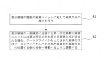
本開示の実施例は更に表示方法を提供し、表示領域の複数の画素ユニットに対して画素欠点の検出を行うことと、表示領域の一側縁部に近接する第1所定個数の画素ユニットには第2所定比率を超える画素欠点が含まれる場合、ゲートドライバから出力された画素行又はソースドライバから出力された画素列が画素欠点の位置する側の対側へ移動するように調整することと、を含む。 An embodiment of the present disclosure further provides a display method, including detecting pixel defects for a plurality of pixel units in a display area, and, when a first predetermined number of pixel units adjacent to one side edge of the display area include pixel defects exceeding a second predetermined ratio, adjusting a pixel row output from a gate driver or a pixel column output from a source driver to move to an opposite side to the side where the pixel defects are located.
いくつかの可能な実現方式では、前記表示領域の一側縁部に近接する第1所定個数の画素ユニットには第2所定比率を超える画素欠点が含まれる場合、ゲートドライバから出力された画素行又はソースドライバから出力された画素列が画素欠点の位置する側の対側へ移動するように調整することは、
初期表示の時、前記ゲートドライバ及びソースドライバがA行目~B行目、C列目~D列目の画素ユニットを駆動して表示させることと、
前記表示領域の左側縁部に近接するC列目~(C+N)列目の画素ユニットには第2所定比率を超える画素欠点が含まれる場合、ソースドライバから出力された画素列を(C+N+1)列目~(D+N+1)列目に調整することと、
前記表示領域の右側縁部に近接する(D-N)列目~D列目の画素ユニットには第2所定比率を超える画素欠点が含まれる場合、ソースドライバから出力された画素列を(C-N-1)列目~(D-N-1)列目に調整することと、
前記表示領域の上側縁部に近接するA行目~(A+M)行目の画素ユニットには第2所定比率を超える画素欠点が含まれる場合、ゲートドライバから出力された画素行を(A+M+1)行目~(B+M+1)行目に調整することと、
前記表示領域の下側縁部に近接する(B-M)行目~B行目の画素ユニットには第2所定比率を超える画素欠点が含まれる場合、ゲートドライバから出力された画素行を(A-M-1)行目~(B-M-1)行目に調整することと、を含み、
A、B、C、D、N及びMがいずれも1以上の自然数であり、且つA<B、C<D、N<C、M<Aである。
In some possible implementations, when a first predetermined number of pixel units adjacent to one side edge of the display area include pixel defects exceeding a second predetermined ratio, adjusting pixel rows output from a gate driver or pixel columns output from a source driver to move to an opposite side of the pixel defects;
During initial display, the gate driver and the source driver drive the pixel units in rows A to B and columns C to D to display;
When the pixel units in columns C to (C+N) adjacent to the left edge of the display area include pixel defects exceeding a second predetermined ratio, the pixel columns output from the source driver are adjusted to columns C+N+1 to (D+N+1);
When the pixel units in the (D-N)th to (D)th columns adjacent to the right edge of the display area include pixel defects exceeding a second predetermined ratio, the pixel columns output from the source driver are adjusted to the (C-N-1)th to (D-N-1)th columns;
When the pixel units in the Ath row to the (A+M)th row adjacent to the upper edge of the display area include pixel defects exceeding a second predetermined ratio, the pixel rows output from the gate driver are adjusted to the (A+M+1)th row to the (B+M+1)th row;
When the pixel units in the (B-M)th row to the (B-M)th row adjacent to the lower edge of the display area include pixel defects exceeding a second predetermined ratio, adjusting the pixel rows output from the gate driver to the (A-M-1)th row to the (B-M-1)th row;
A, B, C, D, N, and M are all natural numbers greater than or equal to 1, and A<B, C<D, N<C, and M<A.
いくつかの可能な実現方式では、前記表示領域の複数の画素ユニットに対して画素欠点の検出を行うことは、前記表示領域の複数の画素ユニットをグループ分けすることと、複数のグループを駆動して順次発光させることと、各グループが発光するとき、該グループにおける画素ユニットが発光するかどうかによって、該グループに画素欠点が含まれるかどうか及び含まれる画素欠点の数を決定することと、を含む。 In some possible implementations, detecting pixel defects for a plurality of pixel units of the display area includes grouping the plurality of pixel units of the display area, driving the plurality of groups to emit light sequentially, and when each group emits light, determining whether the group contains pixel defects and the number of pixel defects contained therein depending on whether the pixel units in the group emit light.
図面の概要及び本開示の実施形態を閲覧して理解した後、他の態様を分かることができる。 After reviewing and understanding the outline drawings and embodiments of the present disclosure, other aspects can be understood.
本開示の目的、技術案及び利点をより明確にするために、以下に図面を参照しながら本開示の実施例を詳しく説明する。実施形態は複数の異なる形式で実施されてもよい。当業者が容易に理解できる事実は、本開示の趣旨及びその範囲を逸脱せずに、方式及び内容を様々な形式に変換することができることである。従って、本開示は下記実施形態に記載の内容のみに限定されると解釈されるべきではない。衝突しない限り、本開示の実施例及び実施例の特徴は互いに任意に組み合わせられることができる。 In order to clarify the objectives, technical solutions and advantages of the present disclosure, the following detailed description of the embodiments of the present disclosure is provided with reference to the drawings. The embodiments may be implemented in a number of different forms. Those skilled in the art can easily understand that the manner and content of the present disclosure can be transformed into various forms without departing from the spirit and scope of the present disclosure. Therefore, the present disclosure should not be construed as being limited to only the contents described in the following embodiments. The embodiments and features of the embodiments of the present disclosure can be combined with each other in any combination, unless there is a conflict.
図面において、明確にするために、各構成要素のサイズ、層の厚さ又は領域を拡大して示す場合がある。従って、本開示の実施形態は該サイズに限定されるとは限らず、図面における各部材の形状及びサイズは真の比率を反映しない。また、図面に理想的な例を模式的に示すが、本開示の実施形態は図面に示される形状又は数値に限定されるものではない。 In the drawings, the size, layer thickness, or area of each component may be enlarged for clarity. Therefore, the embodiments of the present disclosure are not necessarily limited to the sizes, and the shapes and sizes of each member in the drawings do not reflect true proportions. In addition, although the drawings show ideal examples in a schematic manner, the embodiments of the present disclosure are not limited to the shapes or values shown in the drawings.
本明細書における「第1」、「第2」、「第3」等の序数用語は構成要素の混同を回避するために設定されたものであり、数の面で限定するためのものではない。 In this specification, ordinal terms such as "first," "second," and "third" are used to avoid confusion between components and are not intended to be limiting in terms of number.
本明細書において、便宜上、「中央部」、「上」、「下」、「前」、「後」、「鉛直」、「水平」、「頂」、「底」、「内」、「外」等の方位又は位置関係を示す言葉を使用して図面を参照しながら構成要素の位置関係を説明することは、本明細書を説明しやすくして説明を簡素化するためのものに過ぎず、指す装置又は素子が必ず特定の方位を有し、特定の方位で構成及び操作しなければならないことを指示又は暗示するものではなく、従って、本開示を制限するものと理解されるべきではない。構成要素の位置関係は各構成要素を説明する方向によって適切に変化する。従って、明細書に説明される言葉に限定されず、状況に応じて適切に取り替えることができる。 In this specification, for convenience, the positional relationship of components is described with reference to the drawings using words indicating orientation or positional relationship such as "center," "upper," "lower," "front," "rear," "vertical," "horizontal," "top," "bottom," "inside," and "outer." This is merely for the purpose of making this specification easier to explain and simplifying the description, and does not indicate or imply that the device or element referred to necessarily has a specific orientation and must be configured and operated in a specific orientation, and therefore should not be understood as limiting the present disclosure. The positional relationship of components changes appropriately depending on the direction in which each component is described. Therefore, it is not limited to the words described in the specification, and can be appropriately replaced depending on the situation.
本明細書において、特に明確に規定及び限定しない限り、用語の「取付」、「接続」、「連結」は広義的に理解されるべきである。例えば、固定接続、又は取り外し可能な接続、又は一体接続であってもよく、機械的接続、又は接続であってもよく、直接接続、又は中間素子による間接接続、又は2つの素子の内部の連通であってもよい。当業者であれば、具体的な状況に応じて上記用語の本開示における具体的な意味を理解することができる。 In this specification, unless otherwise clearly specified and limited, the terms "attached," "connected," and "coupled" should be understood in a broad sense. For example, they may be fixedly connected, or detachably connected, or integrally connected, or may be mechanically connected or connected, or may be direct connected, or indirectly connected through an intermediate element, or internally connected between two elements. Those skilled in the art can understand the specific meaning of the above terms in this disclosure according to the specific circumstances.
本明細書において、トランジスタとは少なくともゲート電極、ドレイン電極及びソース電極の3つの端子を備える素子を指す。トランジスタはドレイン電極(ドレイン電極端子、ドレイン領域又はドレイン電極)とソース電極(ソース電極端子、ソース領域又はソース電極)との間にチャネル領域を有し、且つ電流はドレイン電極、チャネル領域及びソース電極を流れることができる。本明細書において、チャネル領域とは電流が主に流れる領域を指す。 In this specification, a transistor refers to an element having at least three terminals: a gate electrode, a drain electrode, and a source electrode. A transistor has a channel region between a drain electrode (drain electrode terminal, drain region, or drain electrode) and a source electrode (source electrode terminal, source region, or source electrode), and a current can flow through the drain electrode, the channel region, and the source electrode. In this specification, a channel region refers to a region through which a current mainly flows.
本明細書において、第1極がドレイン電極であり、第2極がソース電極であることであってもよく、又は、第1極がソース電極であり、第2極がドレイン電極であることであってもよい。極性が反対であるトランジスタを使用する場合又は回路動作中の電流方向が変化する場合等に、「ソース電極」及び「ドレイン電極」の機能は互いに交換される場合がある。従って、本明細書において、「ソース電極」及び「ドレイン電極」は互いに交換されることができる。 In this specification, the first pole may be a drain electrode and the second pole may be a source electrode, or the first pole may be a source electrode and the second pole may be a drain electrode. The functions of "source electrode" and "drain electrode" may be interchanged, such as when using transistors of opposite polarity or when the current direction during circuit operation changes. Thus, in this specification, "source electrode" and "drain electrode" may be interchanged.
本明細書において、「接続」は構成要素が、ある電気的作用を有する素子により一体に接続される状況を含む。「ある電気的作用を有する素子」は接続される構成要素間の電気信号の授受を行うことができる限り、特に制限しない。「ある電気的作用を有する素子」の例は電極及び配線のほか、更にトランジスタ等のスイッチング素子、抵抗器、インダクタ、コンデンサ、他の様々な機能を持つ素子等を含む。 In this specification, "connection" includes a situation in which components are connected together by an element having a certain electrical function. There are no particular limitations on the "element having a certain electrical function" as long as it is possible to transmit and receive electrical signals between the components being connected. Examples of "elements having a certain electrical function" include electrodes and wiring, as well as switching elements such as transistors, resistors, inductors, capacitors, and other elements with various functions.
本明細書において、「平行」とは2つの直線がなす角度が-10°以上且つ10°以下の状態を指し、従って、該角度が-5°以上且つ5°以下の状態も含む。また、「垂直」とは2つの直線がなす角度が80°以上且つ100°以下の状態を指し、従って、85°以上且つ95°以下の角度の状態も含む。 In this specification, "parallel" refers to a state in which the angle between two lines is greater than or equal to -10° and less than or equal to 10°, and therefore includes a state in which the angle is greater than or equal to -5° and less than or equal to 5°. Also, "perpendicular" refers to a state in which the angle between two lines is greater than or equal to 80° and less than or equal to 100°, and therefore includes a state in which the angle is greater than or equal to 85° and less than or equal to 95°.
本明細書において、「フィルム」及び「層」は互いに交換されることができる。例えば、「導電層」を「導電フィルム」に置換できる場合がある。それと同様に、「絶縁フィルム」を「絶縁層」に置換できる場合がある。 In this specification, the terms "film" and "layer" may be interchanged. For example, a "conductive layer" may be substituted for a "conductive film." Similarly, an "insulating film" may be substituted for an "insulating layer."
シリコン系OLEDマイクロディスプレイの製造過程において、パッケージ、表面実装等のプロセスにより表示モジュールのある辺の表示エリアの一部の画素が破損され、更に表示時に実際に表示する画素点数が予め設計された画素点数より少ないことをもたらす場合がある。 During the manufacturing process of silicon-based OLED microdisplays, some pixels in the display area on one side of the display module may be damaged due to packaging, surface mounting, and other processes, which may result in the number of pixels actually displayed being less than the number of pixels designed in advance.
本開示の少なくとも1つの実施例は表示基板を提供し、該表示基板は表示領域と、表示領域を取り囲むオフセット領域とを備え、表示基板の位置する平面に垂直な方向において、表示基板はシリコン系基板と、シリコン系基板に設置される発光構造層と、発光構造層のシリコン系基板から離れる側に設置されるパッケージ層とを備え、表示領域のシリコン系基板に第1画素駆動回路が集積され、オフセット領域のシリコン系基板に第2画素駆動回路が集積され、第1画素駆動回路は表示領域の発光構造層に接続され、少なくとも一部の第1画素駆動回路は正常に表示するとき、第1画素駆動回路に電気的に接続される発光構造層に駆動信号を提供するように構成され、第2画素駆動回路はオフセット領域の発光構造層に接続され、少なくとも一部の第2画素駆動回路は正常に表示するとき、第2画素駆動回路に電気的に接続される発光構造層に駆動信号を提供しないように構成される。 At least one embodiment of the present disclosure provides a display substrate, the display substrate having a display region and an offset region surrounding the display region, and in a direction perpendicular to a plane on which the display substrate is located, the display substrate has a silicon-based substrate, a light-emitting structure layer disposed on the silicon-based substrate, and a package layer disposed on the side of the light-emitting structure layer away from the silicon-based substrate, a first pixel driving circuit is integrated on the silicon-based substrate of the display region, a second pixel driving circuit is integrated on the silicon-based substrate of the offset region, the first pixel driving circuit is connected to the light-emitting structure layer of the display region, and at least a part of the first pixel driving circuit is configured to provide a driving signal to the light-emitting structure layer electrically connected to the first pixel driving circuit when displaying normally, and the second pixel driving circuit is connected to the light-emitting structure layer of the offset region, and at least a part of the second pixel driving circuit is configured not to provide a driving signal to the light-emitting structure layer electrically connected to the second pixel driving circuit when displaying normally.
本開示のいくつかの実施例は上記表示基板に対応する表示装置及び表示方法を更に提供する。 Some embodiments of the present disclosure further provide a display device and a display method corresponding to the above-mentioned display substrate.
本開示の上記実施例に係る表示基板によれば、オフセット領域を設置することにより、パッケージ、表面実装等のプロセスにより表示モジュールのある縁部の表示領域の一部の画素ユニットが破損される場合、実際表示領域の位置がオフセット領域へ移動するように調整して、パッケージ・表面実装により破損された画素ユニットを避けることができ、それにより実際に表示する画素点数が予め設計された画素点数に一致するように確保する。 According to the display substrate of the above embodiment of the present disclosure, by providing an offset region, if some pixel units in the display region at an edge of the display module are damaged due to processes such as packaging and surface mounting, the position of the actual display region can be adjusted to move to the offset region to avoid the pixel units damaged by packaging and surface mounting, thereby ensuring that the number of pixels actually displayed matches the number of pixels designed in advance.
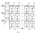
図1は本開示の表示基板の構造模式図である。図1に示すように、本実施例では、該表示基板は表示領域100と、表示領域100を取り囲むオフセット領域200とを備え、表示基板の位置する平面に垂直な方向において、表示基板は、シリコン系基板と、シリコン系基板に設置される発光構造層と、発光構造層のシリコン系基板から離れる側に設置されるパッケージ層とを備え、表示領域のシリコン系基板に第1画素駆動回路が集積され、オフセット領域のシリコン系基板に第2画素駆動回路が集積され、第1画素駆動回路は表示領域の発光構造層に接続され、少なくとも一部の第1画素駆動回路は、正常に表示するとき、第1画素駆動回路に電気的に接続される発光構造層に駆動信号を提供するように構成され、第2画素駆動回路はオフセット領域の発光構造層に接続され、少なくとも一部の第2画素駆動回路は、正常に表示するとき、第2画素駆動回路に電気的に接続される発光構造層に駆動信号を提供しないように構成される。
Figure 1 is a structural schematic diagram of a display substrate of the present disclosure. As shown in Figure 1, in this embodiment, the display substrate includes a
1つの例示的な実施例では、すべての第1画素駆動回路は、いずれも第1画素駆動回路に電気的に接続される発光構造層に駆動信号を提供するように構成される。 In one exemplary embodiment, all of the first pixel driving circuits are configured to provide driving signals to light-emitting structure layers that are all electrically connected to the first pixel driving circuits.
1つの例示的な実施例では、図1に示すように、表示基板はオフセット領域200を少なくとも部分的に取り囲むダミー画素領域300を更に備えてもよく、表示基板の位置する平面に垂直な方向において、ダミー画素領域300は、シリコン系基板と、シリコン系基板に設置される発光構造層と、前記発光構造層のシリコン系基板から離れる側に設置されるパッケージ層とを備えてもよい。
In one exemplary embodiment, as shown in FIG. 1, the display substrate may further include a
1つの例示的な実施例では、図1に示すように、表示基板はダミー画素領域300を取り囲む陰極リング400を更に備えてもよく、表示基板の位置する平面に垂直な方向において、陰極リング400はシリコン系基板に設置される給電電極層と、給電電極層のシリコン系基板から離れる側に設置される反射層と、反射層の給電電極層から離れる側に設置される陽極層と、陽極層の反射層から離れる側に設置される陰極層とを備えてもよい。
In one exemplary embodiment, as shown in FIG. 1, the display substrate may further include a
1つの例示的な実施例では、図1に示すように、表示領域100は複数の第1画素ユニット101を備え、オフセット領域200は複数の第2画素ユニット201を備え、第2画素ユニット201は第1画素ユニット101の予備画素ユニットとして構成される。
In one exemplary embodiment, as shown in FIG. 1, the
1つの例示的な実施例では、該表示基板はシリコン系OLEDマイクロディスプレイ基板又は他のいかなるタイプの表示基板であってもよい。シリコン系OLEDマイクロディスプレイ基板は単結晶シリコンウエハをアクティブ駆動バックプレートとして用い、高PPI、高度に集積され、体積が小さく、持ちやすく、耐震性が高く、超低消費電力等の優れた特性を有する。 In one exemplary embodiment, the display substrate may be a silicon-based OLED microdisplay substrate or any other type of display substrate. The silicon-based OLED microdisplay substrate uses a single crystal silicon wafer as an active driving backplate, and has excellent properties such as high PPI, high integration, small volume, easy to hold, high vibration resistance, and ultra-low power consumption.
1つの例示的な実施例では、オフセット領域200は左側オフセット領域、右側オフセット領域、上側オフセット領域及び下側オフセット領域のうちのいずれか1つ又は複数を含んでもよく、左側オフセット領域及び右側オフセット領域に含まれる画素ユニット列数の差分は10行を超えず、上側オフセット領域及び下側オフセット領域に含まれる画素ユニット行数の差分は10行を超えない。
In one exemplary embodiment, the offset
1つの例示的な実施例では、左側オフセット領域及び右側オフセット領域に含まれる画素ユニット列数は同じであってもよい。 In one exemplary embodiment, the number of pixel unit columns included in the left offset region and the right offset region may be the same.
図2に示すように、表示領域100の左側縁部に近接する第1画素ユニット101には第2所定比率を超える画素欠点102が含まれる場合、ソースドライバから出力された画素列が右側へ移動するように調整し、即ち実際表示領域は右へ移動する。同様に、表示領域100の右側縁部に近接する第1画素ユニット101には第2所定比率を超える画素欠点102が含まれる場合、ソースドライバから出力された画素列が左側へ移動するように調整し、即ち実際表示領域は左へ移動する。
As shown in FIG. 2, if the
1つの例示的な実施例では、左側オフセット領域の第2画素ユニットの列数と表示領域の第1画素ユニットの列数との比率は1%以上であり、右側オフセット領域の第2画素ユニットの列数と表示領域の第1画素ユニットの列数との比率は1%以上である。例示的に、表示領域に1920行*1080列の第1画素ユニットが含まれる場合、左側オフセット領域に含まれる第2画素ユニットの列数は0列~16列であり、右側オフセット領域に含まれる第2画素ユニットの列数は0列~16列である。合理的な数の第2画素ユニットを設置することにより、表示基板の実際表示空間が浪費されないようにするとともに、一定の候補表示空間を保持させ、所定表示領域の第1画素ユニットの縁部が破損される場合に使用に備える。 In one exemplary embodiment, the ratio of the number of columns of the second pixel units in the left offset region to the number of columns of the first pixel units in the display region is 1% or more, and the ratio of the number of columns of the second pixel units in the right offset region to the number of columns of the first pixel units in the display region is 1% or more. Exemplarily, when the display region includes first pixel units of 1920 rows x 1080 columns, the number of columns of the second pixel units included in the left offset region is 0 to 16 columns, and the number of columns of the second pixel units included in the right offset region is 0 to 16 columns. By providing a reasonable number of second pixel units, the actual display space of the display substrate is not wasted, and a certain candidate display space is maintained to prepare for use when the edge of the first pixel units in a given display region is damaged.
1つの例示的な実施例では、上側オフセット領域及び下側オフセット領域に含まれる画素ユニット行数は同じであってもよい。 In one exemplary embodiment, the number of pixel unit rows included in the upper offset region and the lower offset region may be the same.
図3に示すように、表示領域100の下側縁部に近接する第1画素ユニット101には第2所定比率を超える画素欠点102が含まれる場合、ゲートドライバから出力された画素行が上側へ移動するように調整し、即ち実際表示領域は上へ移動する。同様に、表示領域100の上側縁部に近接する第1画素ユニット101には第2所定比率を超える画素欠点102が含まれる場合、ゲートドライバから出力された画素行が下側へ移動するように調整し、即ち実際表示領域は下へ移動する。
As shown in FIG. 3, if the
1つの例示的な実施例では、上側オフセット領域の第2画素ユニットの行数と表示領域の第1画素ユニットの行数との比率は1%以上であり、下側オフセット領域の第2画素ユニットの行数と表示領域の第1画素ユニットの行数との比率は1%以上である。例示的に、表示領域に1920行*1080列の第1画素ユニットが含まれる場合、上側オフセット領域に含まれる第2画素ユニットの行数は0行~16行であり、下側オフセット領域に含まれる第2画素ユニットの行数は0行~16行である。合理的な数の第2画素ユニットを設置することにより、表示基板の実際表示空間が浪費されないようにするとともに、一定の候補表示空間を保持させ、所定表示領域の第1画素ユニットの縁部が破損される場合に使用に備える。 In one exemplary embodiment, the ratio of the number of rows of the second pixel units in the upper offset region to the number of rows of the first pixel units in the display region is 1% or more, and the ratio of the number of rows of the second pixel units in the lower offset region to the number of rows of the first pixel units in the display region is 1% or more. For example, if the display region includes 1920 rows x 1080 columns of first pixel units, the number of rows of the second pixel units included in the upper offset region is 0 to 16 rows, and the number of rows of the second pixel units included in the lower offset region is 0 to 16 rows. By providing a reasonable number of second pixel units, the actual display space of the display substrate is not wasted, and a certain candidate display space is maintained to prepare for use when the edge of the first pixel units in a given display region is damaged.
本実施例では、図4に示すように、表示基板に垂直な平面において、表示基板の表示領域100及びオフセット領域200は、それぞれシリコン系基板10と、シリコン系基板10に設置される発光構造層20と、発光構造層20に設置されるパッケージ層40と、パッケージ層40に設置されるカラーフィルム層50とを備える。表示基板の表示領域100及びオフセット領域200のシリコン系基板10には、駆動信号を生成するための画素駆動回路、ゲート駆動信号を生成するためのゲート駆動回路、及びデータ信号を生成するためのデータ駆動回路が集積される。発光構造層20は、シリコン系基板10に積層される反射層、陽極層、有機発光層及び陰極層を備え、反射層は陰極層とマイクロキャビティ構造を構成することに用いられ、有機発光層から直接射出された光と反射層により反射された光とを互いに干渉させ、射出光の色域を向上させ、射出光の輝度を強化する。例示的な実施形態では、発光構造層20は更に画素定義層又は平坦層等の構造フィルム層を備えてもよい。パッケージ層40が発光構造層20を包むことは、パッケージ層40が発光構造層20のシリコン系基板10から離れる側の上面に設置され、及び発光構造層20のすべての側面に設置され、パッケージ層40とシリコン系基板10により密閉されたチャンバーが構成され、発光構造層20が該密閉されたチャンバー内に設置されることを意味する。シリコン系基板10に平行する平面及びシリコン系基板10に垂直な平面において、パッケージ層40のシリコン系基板10での正投影は、発光構造層20のシリコン系基板10での正投影を含む。
In this embodiment, as shown in FIG. 4, in a plane perpendicular to the display substrate, the
1つの例示的な実施例では、表示領域100及びオフセット領域200のカラーフィルム層50は、それぞれアレイ状に設置される第1色ユニット53、第2色ユニット54及び第3色ユニット55を備え、第1色ユニット53、第2色ユニット54及び第3色ユニット55は、それぞれ赤(R)色カラーフィルタユニット(CF、Color Filter)、緑(G)色カラーフィルタユニット及び青(B)色カラーフィルタユニットのうちの1つであってもよい。いくつかの可能な実現方式では、カラーフィルム層50における色ユニットは互いにオーバーラップしてブラックマトリックスとされてもよく、又は色ユニットの間にブラックマトリックスを設置する。本開示は白色光+カラーフィルムの方式を用いて、2000より大きな高解像度を実現することができ、VR/ARニーズを満足することができる。
In one exemplary embodiment, the
1つの例示的な実施例では、有機発光層33のうちの少なくとも1層は全面的に設置されてもよく、又は独立して各画素領域に応じて設置されてもよく、各画素領域における各色の発光層が積層されて白色光を発することができればよい。
In one exemplary embodiment, at least one of the organic light-emitting
1つの例示的な実施例では、有機発光層33は、赤、緑、青の3つの色の発光層がそれぞれアレイ状に配置されるものであってもよく、各画素領域から独立して赤色光、青色光、緑色光を発する。
In one exemplary embodiment, the organic light-emitting
1つの例示的な実施例では、ダミー画素領域300がカラーフィルム構造を備えず、例えば基板におけるある側のオフセット領域200における表示ユニットが使用されていない場合、オフセット領域200における表示ユニットの上方のカラーフィルム層はダミーカラーフィルムとして、カラーフィルム層の製造時の露光・現像の不均一による不均一問題を緩和することができる。
In one exemplary embodiment, when the
1つの例示的な実施例では、ダミー画素領域300はカラーフィルム構造を備えてもよく、表示領域におけるカラーフィルム層の設置方式と同じであってもよく、本実施例では詳細な説明は省略する。
In one exemplary embodiment, the
1つの例示的な実施例では、陰極リング400の上方にカラーフィルム層が設置されてもよく、該領域のカラーフィルム層は外周領域に延在してもよい。
In one exemplary embodiment, a color film layer may be placed over the
1つの例示的な実施例では、表示基板は更にカバープレート70を備えてもよく、カバープレート70はカラーフィルム層50の上方に設置され、カラーフィルム層50への保護機能を実現することができる。例示的な実施形態では、カバープレート70はシーラントによりシリコン系基板10に接続され、シーラントはシリコン系基板10とカバープレート70との間に設置され、水蒸気と酸素の侵入を阻止するために保障を提供することができ、シリコン系OLED表示基板の耐用年数を大幅に延ばす。他の例示的な実施形態では、シーラントはカバープレート70の側面に設置されてもよく、カバープレート70の周りの側面とシリコン系基板10との間がシーラントにより密封され、シーラントのシリコン系基板10から離れる側の端面は、カバープレート70のシリコン系基板10に隣接する側の表面とカバープレート70のシリコン系基板10から離れる側の表面との間に位置し、これにより、密封効果を確保することができるだけではなく、シーラントがカバープレート70より高いことによる表示基板の厚さの増加を防止することもできる。例示的な実施形態では、カバープレート70は表示領域100に設置され、位置合わせ及び密封を良く実現し、切断過程におけるカバープレート70の割れを回避することができる。
In one exemplary embodiment, the display substrate may further include a cover plate 70, which is disposed above the
1つの例示的な実施例では、表示基板は更に保護層60を備えてもよく、保護層60はカラーフィルム層50とカバープレート70との間に設置され、保護層60はカラーフィルム層50を被覆する。例示的な実施形態では、保護層60はSiC又はSiCNxを用いてもよく、SiC又はSiCNxが無機特性を有する傾向があるため、カラーフィルム層50を保護することができ、カラーフィルム層50の劣化損傷を減少させ、耐用年数を延ばす一方、平坦表面を形成することができ、後続のカバープレートの貼合プロセスにおける接着剤のレベリングを容易にし、カバープレートの貼合品質を向上させる。
In one exemplary embodiment, the display substrate may further include a
図5は本開示のシリコン系基板の回路原理の模式図である。シリコン系基板10は表示領域100(AAエリア)及びオフセット領域200に位置する複数の表示ユニットと、外周領域に位置する制御回路とを備え、表示領域100における複数の表示ユニットは規則的に配置され、複数の表示行及び複数の表示列を形成し、各表示ユニットは画素駆動回路103と、画素駆動回路103に接続される発光デバイス104とを備え、画素駆動回路103は少なくとも駆動トランジスタを備える。制御回路は少なくとも複数の電圧制御回路110を備え、各電圧制御回路110は複数の画素駆動回路103に接続される。例えば、1つの電圧制御回路110は1つの表示行における画素駆動回路103に接続され、該表示行の画素駆動回路103における駆動トランジスタの第1極は共同で該電圧制御回路110に接続され、各駆動トランジスタの第2極はこの表示ユニットの発光デバイス104の陽極に接続され、発光デバイス104の陰極は第2電源信号VSSの入力端子に接続される。電圧制御回路110はそれぞれ第1電源信号VDDの入力端子、初期化信号Vinitの入力端子、リセット制御信号REの入力端子及び発光制御信号EMの入力端子に接続され、電圧制御回路110は、リセット制御信号REに応答して、初期化信号Vinitを駆動トランジスタの第1極に出力して、対応の発光デバイス104をリセットするように制御するように構成される。電圧制御回路110は更に、発光制御信号EMに応答して、第1電源信号VDDを駆動トランジスタの第1極に出力して、発光デバイス104を駆動して発光させるように構成される。1つの表示行における画素駆動回路103は共同で電圧制御回路110に接続されることにより、表示領域100における各画素駆動回路103の構造を簡素化し、表示領域100における画素駆動回路103の占有面積を低減することができ、これにより、より多くの画素駆動回路103及び発光デバイス104を表示領域100に設置し、高PPI表示を実現する。電圧制御回路110は、リセット制御信号REの制御によって初期化信号Vinitを駆動トランジスタの第1極に出力し、対応の発光デバイス104をリセットするように制御し、前のフレームが発光する際に発光デバイス104に印加した電圧の次のフレームによる発光への影響を回避することができ、残影現象を改善することができる。
5 is a schematic diagram of the circuit principle of the silicon-based substrate of the present disclosure. The silicon-based
例示的な実施形態では、3つの異なる色の表示ユニットにより1つの画素ユニットが構成され(該画素ユニットは第1画素ユニットであってもよく、又は第2画素ユニットであってもよい)、3つの表示ユニットはそれぞれ赤色表示ユニット、緑色表示ユニット及び青色表示ユニットであってもよい。いくつかの可能な実現方式では、1つの画素ユニットは4つ、5つまたはより多くの表示ユニットを備えてもよく、実際の応用環境に応じて設計して決定されてもよく、ここで制限しない。いくつかの可能な実現方式では、1つの電圧制御回路110は、同一の表示行における2つの隣接する表示ユニットの画素駆動回路103に接続されてもよく、又は同一の表示行における3つまたはより多くの表示ユニットの画素駆動回路103に接続されてもよく、ここで制限しない。
In an exemplary embodiment, one pixel unit is composed of three different color display units (the pixel unit may be the first pixel unit or the second pixel unit), and the three display units may be a red display unit, a green display unit and a blue display unit, respectively. In some possible implementations, one pixel unit may have four, five or more display units, which may be designed and determined according to the actual application environment, and is not limited here. In some possible implementations, one
図6は本開示の電圧制御回路及び画素駆動回路の回路実現の模式図である。図6に示すように、発光デバイスはOLEDを備えてもよく、OLEDの陽極は駆動トランジスタM0の第2極Dに接続され、OLEDの陰極は第2電源信号VSSの入力端子に接続され、第2電源信号VSSの電圧は一般的に負電圧又は接地電圧VGND(一般的に0Vである)であり、初期化信号Vinitの電圧は接地電圧VGNDとして設定されてもよい。例示的な実施形態では、OLEDはMicro-OLED又はMini-OLEDであってもよく、高PPI表示を実現することに役立つ。 6 is a schematic diagram of a circuit implementation of the voltage control circuit and pixel driving circuit of the present disclosure. As shown in FIG. 6, the light emitting device may include an OLED, the anode of the OLED is connected to the second pole D of the driving transistor M0, and the cathode of the OLED is connected to the input terminal of the second power supply signal VSS, the voltage of the second power supply signal VSS is generally a negative voltage or a ground voltage VGND (generally 0V), and the voltage of the initialization signal Vinit may be set as the ground voltage VGND . In an exemplary embodiment, the OLED may be a Micro-OLED or Mini-OLED, which is useful for realizing a high PPI display.
例示的な実施形態では、電圧制御回路110は1つの表示行における2つの画素駆動回路103に接続され、画素駆動回路103は駆動トランジスタM0、第3トランジスタM3、第4トランジスタM4及び蓄電コンデンサCstを備え、電圧制御回路110は第1トランジスタM1及び第2トランジスタM2を備える。駆動トランジスタM0、第1トランジスタM1、第2トランジスタM2、第3トランジスタM3、第4トランジスタM4は、いずれもシリコン系基板に製造された金属酸化物半導体電界効果トランジスタ(MOS、Metal Oxide Semiconductor)である。
In an exemplary embodiment, the
第1トランジスタM1の制御電極はリセット制御信号REの入力端子に接続され、リセット制御信号REを受信することに用いられ、第1トランジスタM1の第1極は初期化信号Vinitの入力端子に接続され、初期化信号Vinitを受信することに用いられ、第1トランジスタM1の第2極はそれぞれ対応の駆動トランジスタM0の第1極S及び第2トランジスタM2の第2極に接続される。第2トランジスタM2の制御電極は発光制御信号EMの入力端子に接続され、発光制御信号EMを受信することに用いられ、第2トランジスタM2の第1極は第1電源信号VDDの入力端子に接続され、第1電源信号VDDを受信することに用いられ、第2トランジスタM2の第2極はそれぞれ対応の駆動トランジスタM0の第1極S及び第1トランジスタM1の第2極に接続される。例示的な実施形態では、第1トランジスタM1及び第2トランジスタM2のタイプは異なってもよく、例えば、第1トランジスタM1はN型トランジスタであり、第2トランジスタM2はP型トランジスタであり、又は、第1トランジスタM1はP型トランジスタであり、第2トランジスタM2はN型トランジスタである。いくつかの可能な実現方式では、第1トランジスタM1及び第2トランジスタM2のタイプは同じであってもよく、実際の応用環境に応じて設計して決定されてもよく、ここで制限しない。 The control electrode of the first transistor M1 is connected to the input terminal of the reset control signal RE and is used to receive the reset control signal RE, the first pole of the first transistor M1 is connected to the input terminal of the initialization signal Vinit and is used to receive the initialization signal Vinit, and the second pole of the first transistor M1 is connected to the first pole S of the corresponding driving transistor M0 and the second pole of the second transistor M2. The control electrode of the second transistor M2 is connected to the input terminal of the light emission control signal EM and is used to receive the light emission control signal EM, the first pole of the second transistor M2 is connected to the input terminal of the first power signal VDD and is used to receive the first power signal VDD, and the second pole of the second transistor M2 is connected to the first pole S of the corresponding driving transistor M0 and the second pole of the first transistor M1. In an exemplary embodiment, the types of the first transistor M1 and the second transistor M2 may be different, for example, the first transistor M1 is an N-type transistor and the second transistor M2 is a P-type transistor, or the first transistor M1 is a P-type transistor and the second transistor M2 is an N-type transistor. In some possible implementations, the types of the first transistor M1 and the second transistor M2 may be the same, and may be determined by design according to the actual application environment, and are not limited here.
画素駆動回路103は駆動トランジスタM0、第3トランジスタM3、第4トランジスタM4及び蓄電コンデンサCstを備える。駆動トランジスタM0の制御電極G、駆動トランジスタM0の第1極Sは第1トランジスタM1の第2極及び第2トランジスタM2の第2極に接続され、駆動トランジスタM0の第2極DはOLEDの陽極に接続される。第3トランジスタM3の制御電極は第1制御電極走査信号S1の入力端子に接続され、第1制御電極走査信号S1を受信することに用いられ、第3トランジスタM3の第1極はデータ信号DAの入力端子に接続され、データ信号DAを受信することに用いられ、第3トランジスタM3の第2極は駆動トランジスタM0の制御電極Gに接続される。第4トランジスタM4の制御電極は第2制御電極走査信号S2の入力端子に接続され、第2制御電極走査信号S2を受信することに用いられ、第4トランジスタM4の第1極はデータ信号DAの入力端子に接続され、データ信号DAを受信することに用いられ、第4トランジスタM4の第2極は駆動トランジスタM0の制御電極Gに接続される。蓄電コンデンサCstの第1端子は駆動トランジスタM0の制御電極Gに接続され、蓄電コンデンサCstの第2端子は接地端子GNDに接続される。例示的な実施形態では、駆動トランジスタM0はN型トランジスタであってもよく、第3トランジスタM3及び第4トランジスタM4のタイプは異なってもよく、例えば、第3トランジスタM3はN型トランジスタであり、第4トランジスタM4はP型トランジスタである。データ信号DAの電圧が高グレースケールに対応する電圧である場合、P型の第4トランジスタM4をオンにすることによりデータ信号DAを駆動トランジスタM0の制御電極Gに伝送し、データ信号DAの電圧が例えばN型の第3トランジスタM3の閾値電圧から影響を受けることを回避することができる。データ信号DAの電圧が低グレースケールに対応する電圧である場合、N型の第3トランジスタM3をオンにすることによりデータ信号DAを駆動トランジスタM0の制御電極Gに伝送し、データ信号DAの電圧がP型の第4トランジスタM4の閾値電圧から影響を受けることを回避することができる。そうすると、駆動トランジスタM0の制御電極Gに入力された電圧範囲を広げることができる。いくつかの可能な実現方式では、第3トランジスタM3及び第4トランジスタM4のタイプについて、第3トランジスタM3はP型トランジスタであってもよく、第4トランジスタM4はN型トランジスタであってもよい。いくつかの可能な実現方式では、画素駆動回路は3T1C、5T1C又は7T1C回路構造であってもよく、又は内部補償又は外部補償機能を有する回路構造であってもよく、本開示はこれを制限しない。
The
以下、表示基板の製造過程の例によって表示基板の構造について説明する。本開示の所謂「パターニングプロセス」はフィルム層の堆積、フォトレジストのコーティング、マスクの露光、現像、エッチング及びフォトレジストの剥離処理を含む。堆積はスパッタリング、蒸着及び化学気相堆積のうちのいずれか1つ又は複数を用いてもよく、コーティングはスプレー及びスピンコートのうちのいずれか1つ又は複数を用いてもよく、エッチングはドライエッチング及びウェットエッチングのうちのいずれか1つ又は複数を用いてもよい。「薄膜」とはある材料を基板に堆積又はコーティングプロセスにより製造した1層の薄膜を指す。製造過程全体において該「薄膜」がパターニングプロセスを行う必要がない場合、該「薄膜」は更に「層」と称されてもよい。製造過程全体において該「薄膜」がパターニングプロセスを行う必要がある場合、パターニングプロセスの前に「薄膜」と称され、パターニングプロセスの後で「層」と称される。パターニングプロセスを経た後の「層」には少なくとも1つの「パターン」が含まれる。本開示で言われる「AとBが同一層に設置される」とは、AとBが同一のパターニングプロセスにより同時に形成されることを意味する。本開示で言われる「Aの正投影がBの正投影を含む」とは、Bの正投影がAの正投影範囲内に位置し、又はAの正投影がBの正投影を被覆することを意味する。 The structure of the display substrate will be described below by taking an example of the manufacturing process of the display substrate. The so-called "patterning process" of the present disclosure includes deposition of a film layer, coating of a photoresist, mask exposure, development, etching, and photoresist stripping. The deposition may be any one or more of sputtering, evaporation, and chemical vapor deposition, the coating may be any one or more of spraying and spin coating, and the etching may be any one or more of dry etching and wet etching. A "thin film" refers to a layer of a thin film produced by depositing a material on a substrate or by a coating process. If the "thin film" does not need to undergo a patterning process during the entire manufacturing process, the "thin film" may further be referred to as a "layer". If the "thin film" needs to undergo a patterning process during the entire manufacturing process, it is referred to as a "thin film" before the patterning process and as a "layer" after the patterning process. The "layer" after the patterning process includes at least one "pattern". In this disclosure, "A and B are disposed in the same layer" means that A and B are formed simultaneously by the same patterning process. In this disclosure, "the orthogonal projection of A includes the orthogonal projection of B" means that the orthogonal projection of B is located within the orthogonal projection range of A, or the orthogonal projection of A covers the orthogonal projection of B.
(1)シリコン系基板10を製造し、図7に示すように、シリコン系基板10は表示領域100と、表示領域100を取り囲む外周領域とを備え、外周領域はオフセット領域200、ダミー画素領域300及び陰極リング400を備え、表示領域100及びオフセット領域200のシリコン系基板10にいずれも画素駆動回路が集積され、陰極リング400のシリコン系基板10に給電回路が集積される。例示的な説明として、図7には表示領域100の3つの表示ユニット、即ち第1最優先表示ユニット、第2最優先表示ユニット及び第3最優先表示ユニットを示し、オフセット領域200の3つの表示ユニット、即ち第1候補表示ユニット、第2候補表示ユニット及び第3候補表示ユニットを示し、画素駆動回路に含まれる駆動トランジスタ11を示し、陰極リング400の給電電極401を示す。例示的な実施形態では、表示領域100及びオフセット領域200の駆動薄膜トランジスタはそれぞれ活性層、ゲート電極、ソース電極、ドレイン電極及びゲート接続電極を備え、ソース電極及びドレイン電極はそれぞれ導電性ピラーによって活性層に接続され、ゲート接続電極は導電性ピラーによってゲート電極に接続される。シリコン系基板10の製造は成熟したCMOS集積回路プロセスを用いてもよく、本開示はこれを制限しない。製造が完了した後、シリコン系基板10の表面には表示領域100のソース電極、ドレイン電極及びゲート接続電極、オフセット領域200のソース電極、ドレイン電極及びゲート接続電極、陰極リング400の給電電極401が露出する。
(1) A silicon-based
(2)シリコン系基板10に第1絶縁薄膜を堆積し、パターニングプロセスにより第1絶縁薄膜をパターニングして、シリコン系基板10を被覆する第1絶縁層12のパターンを形成し、表示領域100及びオフセット領域200の第1絶縁層12にそれぞれ複数の第1ビアを形成し、陰極リング400の第1絶縁層12に少なくとも1つの第2ビアを形成し、複数の第1ビアがそれぞれ各表示ユニットのドレイン電極を露出させ、第2ビアが給電電極401を露出させる。その後、図8に示すように、第1絶縁層12における第1ビア及び第2ビア内に複数の第1導電性ピラー13を形成し、第1ビアにおける第1導電性ピラー13はその位置する表示ユニットのドレイン電極に接続され、第2ビアにおける第1導電性ピラー13は陰極リング400の給電電極401に接続される。例示的な実施形態では、第1導電性ピラー13は金属材料により製造されてもよく、充填処理により第1導電性ピラー13を形成した後、更に研磨処理することができ、研磨プロセスにより第1絶縁層12及び第1導電性ピラー13の表面を腐食して摩擦して、第1絶縁層12及び第1導電性ピラー13の一部の厚さを除去し、第1絶縁層12及び第1導電性ピラー13に面一の表面を形成させる。いくつかの可能な実現方式では、第1導電性ピラー13は金属タングステン(W)を用いてもよく、タングステン金属で充填されるビアはタングステンビア(W-via)と称される。第1絶縁層12の厚さが比較的大きい場合、タングステンビアを用いることにより導電通路の安定性を確保することができる。タングステンビアの製造プロセスが成熟したため、得られた第1絶縁層12の表面平坦度が高く、接触抵抗の低減に役立つ。タングステンビアはシリコン系基板10と反射層との接続に適用されるだけではなく、反射層と陽極層との接続及び他の配線層間の接続にも適用される。
(2) A first insulating thin film is deposited on the silicon-based
(3)図9に示すように、上記構造が形成されるシリコン系基板10に第1金属薄膜を堆積し、パターニングプロセスにより第1金属薄膜をパターニングし、第1絶縁層12に反射層のパターンを形成し、反射層は表示領域100、オフセット領域200、ダミー画素領域300及び陰極リング400内に設置される複数の反射電極14を備え、各表示ユニットにおいて、反射電極14は第1導電性ピラー13によってドレイン電極に接続され、陰極リング400において、反射電極14は第1導電性ピラー13によって給電電極401に接続される。例示的な実施形態では、各表示ユニットの反射電極14は後続形成される陰極とマイクロキャビティ構造を構成することに用いられ、反射電極の高反射効果を利用して、有機発光層から直接射出された光と反射電極により反射された光とを互いに干渉させ、射出光の色域を向上させ、射出光の輝度を強化する。
(3) As shown in FIG. 9, a first metal thin film is deposited on the silicon-based
(4)上記構造が形成されるシリコン系基板10に第2絶縁薄膜を堆積し、パターニングプロセスにより第2絶縁薄膜をパターニングして、シリコン系基板10を被覆する第2絶縁層15のパターンを形成し、表示領域100及びオフセット領域200の第2絶縁層15にそれぞれ複数の第3ビアを形成し、ダミー画素領域300の第2絶縁層15に複数の第4ビアを形成し、陰極リング400の第2絶縁層15に少なくとも1つの第5ビアを形成し、複数の第3ビアがそれぞれ各表示ユニットの反射電極14を露出させ、複数の第4ビアがそれぞれ各ダミー画素領域300の反射電極14を露出させ、第5ビアが陰極リング400の反射電極14を露出させる。その後、図10に示すように、第2絶縁層15における第3ビア、第4ビア及び第5ビア内に複数の第2導電性ピラー16を形成し、第3ビアにおける第2導電性ピラー16はその位置する表示ユニットの反射電極14に接続され、第4ビアにおける第2導電性ピラー16はダミー画素領域300の反射電極14に接続され、第5ビアにおける第2導電性ピラー16は陰極リング400の反射電極14に接続される。例示的な実施形態では、第2導電性ピラー16は金属材料により製造されてもよく、充填処理により第2導電性ピラー16を形成した後、更に研磨処理することができ、研磨プロセスにより第2絶縁層15及び第2導電性ピラー16の表面を腐食して摩擦して、第2絶縁層15及び第2導電性ピラー16の一部の厚さを除去し、第2絶縁層15及び第2導電性ピラー16に面一の表面を形成させる。いくつかの可能な実現方式では、第2導電性ピラー16は金属タングステン(W)を用いてもよい。
(4) A second insulating thin film is deposited on the silicon-based
(5)図11に示すように、上記構造が形成されるシリコン系基板10に透明導電薄膜を堆積し、パターニングプロセスにより透明導電薄膜をパターニングし、表示領域100、オフセット領域200、ダミー画素領域300及び陰極リング400の第2絶縁層15にそれぞれ陽極層のパターンを形成し、陽極層は表示領域100、オフセット領域200、ダミー画素領域300及び陰極リング400に設置される複数の陽極31を備え、陽極31は第2導電性ピラー16によって反射電極14に接続される。本開示では、陽極31は第2導電性ピラー16によって反射電極14に接続され、反射電極14は第1導電性ピラー13によって駆動薄膜トランジスタ11のドレイン電極に接続され、そうすると、画素駆動回路の提供する電気信号は反射電極14を介して陽極31に伝送され、反射電極14は画素駆動回路と陽極との間の導電通路を形成する一方、マイクロキャビティ構造を形成し、画素駆動回路の発光デバイスに対する制御に役立つだけではなく、表示基板の構造をよりコンパクトにし、シリコン系OLED表示装置の小型化にも役立つ。
(5) As shown in FIG. 11, a transparent conductive thin film is deposited on the silicon-based
(6)上記構造が形成されるシリコン系基板10に画素定義薄膜をコーティングし、マスク、露光、現像プロセスにより表示領域100、オフセット領域200、ダミー画素領域300及び陰極リング400に画素定義層(PDL)32のパターンを形成し、各表示ユニットにおいて、画素定義層32に画素開口が開設され、画素開口が陽極31の表面を露出させる。その後、図12に示すように、表示領域100、オフセット領域200及びダミー画素領域300に有機発光層33及び陰極34を順次形成し、各表示ユニットにおいて、有機発光層33はその位置する表示ユニットの陽極31に接続され、面状の陰極34は各表示ユニットの有機発光層33に接続され、陰極リング400に陰極34を形成し、陰極リング400の陰極34は画素開口によって陽極31に接続される。例示的な実施形態では、陰極34は半透過半反射電極であり、上記形成される反射電極14とマイクロキャビティ構造を構成する。
(6) A pixel definition thin film is coated on the silicon-based
上記製造過程において、第1絶縁薄膜及び第2絶縁薄膜はシリコン酸化物(SiOx)、シリコン窒化物(SiNx)又は酸窒化ケイ素(SiON)を用いてもよく、単層構造であってもよく、又は多層複合構造であってもよい。第1金属薄膜は金属材料、例えば銀(Ag)、銅(Cu)、アルミニウム(Al)又はモリブデン(Mo)等を用いてもよく、又は金属からなる合金材料、例えばアルミニウムネオジム合金(AlNd)又はモリブデンニオブ合金(MoNb)等を用いてもよく、合金材料は単層構造であってもよく、又は多層複合構造例えばMo/Cu/Moの複合構造であってもよい。透明導電薄膜は酸化インジウムスズ(ITO)又は酸化インジウム亜鉛(IZO)、又はITO/Ag/ITOの複合構造を用いてもよく、画素定義層はポリイミド、アクリル又はポリエチレンテレフタレート等を用いてもよい。 In the above manufacturing process, the first insulating thin film and the second insulating thin film may be made of silicon oxide (SiOx), silicon nitride (SiNx) or silicon oxynitride (SiON), and may be a single-layer structure or a multi-layer composite structure. The first metal thin film may be made of a metal material, such as silver (Ag), copper (Cu), aluminum (Al) or molybdenum (Mo), or may be made of an alloy material made of a metal, such as an aluminum neodymium alloy (AlNd) or a molybdenum niobium alloy (MoNb), and the alloy material may be a single-layer structure or a multi-layer composite structure, such as a Mo/Cu/Mo composite structure. The transparent conductive thin film may be made of indium tin oxide (ITO) or indium zinc oxide (IZO), or a composite structure of ITO/Ag/ITO, and the pixel definition layer may be made of polyimide, acrylic, or polyethylene terephthalate, etc.
(7)図13に示すように、上記構造が形成されるシリコン系基板10において、表示領域100、オフセット領域200、ダミー画素領域300及び陰極リング400にパッケージ層のパターンを形成し、パッケージ層40は薄膜パッケージ構造である。
(7) As shown in FIG. 13, in the silicon-based
(8)図14に示すように、上記構造が形成されるシリコン系基板10において、表示領域100、オフセット領域200、ダミー画素領域300及び陰極リング400にカラーフィルム層50のパターンを形成し、表示領域100及びオフセット領域200のカラーフィルム層50は、互いに間隔を置いて設置され又は互いにオーバーラップして設置される第1色ユニット53、第2色ユニット54及び第3色ユニット55を備え、ダミー画素領域300及び陰極リング400のカラーフィルム層50は、パッケージ層において下から上まで順次積層設置される第1色ユニット53及び第2色ユニット54を備える。例示的な実施形態では、第1色ユニットは緑色ユニットGであってもよく、第2色ユニットは赤色ユニットRであってもよく、第3色ユニットは青色ユニットBであってもよい。いくつかの可能な実現方式では、カラーフィルム層50の製造過程は、まず青色ユニットBを形成し、次に赤色ユニットRを形成し、それから緑色ユニットGを形成することを含む。青色カラーフィルムの接着性が比較的大きく、青色ユニットBを先に形成することによりカラーフィルム層50が陰極から剥離する可能性を低下させることができる。赤色ユニットRの接着性が比較的小さいが、流動性が高いため、赤色ユニットRの形成過程において、青色ユニットB及び赤色ユニットRの陰極から離れる側の表面の気泡数を減少させることができ、それにより青色ユニットB及び赤色ユニットRの両方のオーバーラップ位置での膜厚の均一性を向上させることができる。緑色ユニットGの基材と赤色ユニットRの基材がほぼ同じであるため、緑色ユニットGと赤色ユニットRとの間の接着力が比較的大きく、カラーフィルム層50が陰極から剥離する可能性を低下させることができる。いくつかの可能な実現方式では、カラーフィルム層50は他の色ユニット、例えば白色又は黄色のもの等を備えてもよい。
(8) As shown in FIG. 14, in the silicon-based
後続のプロセスにおいて、密封プロセスを用いてカバープレート70を形成し、カバープレート70とシリコン系基板10はシーラントにより固定される。シリコン系基板10、カバープレート70及びシーラントは密閉された空間を形成するため、水蒸気と酸素を阻止する保障を提供し、シリコン系OLED表示基板の耐用年数を大幅に延ばす。その後、形成された表示マザーボードを切断して、独立した表示基板を形成する。
In the subsequent process, a sealing process is used to form the cover plate 70 , and the cover plate 70 and the silicon-based
図15は本開示の有機発光層の構造模式図である。図15に示すように、本開示の有機発光層の構造は、陽極と陰極との間に順次積層される第1発光サブ層331、第1電荷発生層332、第2発光サブ層333、第2電荷発生層334及び第3発光サブ層335を備える。第1発光サブ層331は第1色光を射出するように設定され、順次積層される第1正孔輸送層(HTL)3311、第1発光材料層(EML)3312及び第1電子輸送層(ETL)3313を備える。第2発光サブ層333は第2色光を射出するように設定され、順次積層される第2正孔輸送層3331、第2発光材料層3332及び第2電子輸送層3333を備える。第3発光サブ層335は第3色光を射出するように設定され、順次積層される第3正孔輸送層3351、第3発光材料層3352及び第3電子輸送層3353を備える。第1電荷発生層332は第1発光サブ層331と第2発光サブ層333との間に設置され、2つの発光サブ層を直列接続してキャリアの伝達を実現することに用いられる。第2電荷発生層334は第2発光サブ層333と第3発光サブ層335との間に設置され、2つの発光サブ層を直列接続してキャリアの伝達を実現することに用いられる。本開示の有機発光層は第1色光を射出する第1発光材料層と、第2色光を射出する第2発光材料層と、第3色光を射出する第3発光材料層とを備えるため、有機発光層が最終的に射出した光は混合光である。例えば、第1発光材料層が赤色光を射出する赤色光材料層であり、第2発光材料層が緑色光を射出する緑色光材料層であり、第3発光材料層が青色光を射出する青色光材料層であるように設定してもよく、従って、有機発光層は最終的に白色光を射出する。
15 is a schematic diagram of the structure of the organic light-emitting layer of the present disclosure. As shown in FIG. 15, the structure of the organic light-emitting layer of the present disclosure includes a first light-emitting
例示的な実施形態では、図15に示される有機発光層は例示的な構造に過ぎず、本開示はこれを制限しない。実際に実施するとき、実際の必要に応じて有機発光層の構造を設計することができる。例えば、各発光サブ層において、電子及び正孔を発光材料層に注入する効率を向上させるために、更に正孔注入層(HIL)及び電子注入層(EIL)を設置してもよい。更に例えば、有機発光層の構造を簡素化するために、第1電子輸送層3313、第1電荷発生層332及び第2正孔輸送層3331をキャンセルしてもよく、即ち第2発光材料層3332は直接に第1発光材料層3312に設置されてもよい。
In the exemplary embodiment, the organic light-emitting layer shown in FIG. 15 is only an exemplary structure, and the present disclosure is not limited thereto. When actually implemented, the structure of the organic light-emitting layer can be designed according to actual needs. For example, in each light-emitting sublayer, a hole injection layer (HIL) and an electron injection layer (EIL) can be further installed to improve the efficiency of injecting electrons and holes into the light-emitting material layer. For example, in order to simplify the structure of the organic light-emitting layer, the first
いくつかの可能な実現方式では、有機発光層は第1色光を射出する有機発光層及び第1色光の相補光を射出する有機発光層を用いてもよく、該2つの有機発光層はシリコン系基板に対して順次積層され、それにより全体的に白色光を発し、本開示はこれを制限せず、白色光を発することを実現できればよい。 In some possible implementations, the organic light-emitting layer may be an organic light-emitting layer that emits a first color light and an organic light-emitting layer that emits the complementary light of the first color light, and the two organic light-emitting layers are sequentially stacked on a silicon-based substrate, thereby emitting white light overall; the present disclosure is not limited to this, and it is sufficient to realize the emission of white light.
本開示の表示基板の構造及びその製造過程から分かるように、オフセット領域を設置することにより、パッケージ、表面実装等のプロセスにより表示モジュールのある縁部の表示領域の一部の第1画素ユニットが破損される場合、実際表示領域の位置がオフセット領域へ移動するように調整して、パッケージ・表面実装により破損された画素ユニットを避けることができ、それにより実際に表示する画素点数が予め設計された画素点数に一致するように確保する。 As can be seen from the structure and manufacturing process of the display substrate disclosed herein, by providing an offset region, if a first pixel unit in a part of the display area at an edge of the display module is damaged due to processes such as packaging and surface mounting, the position of the actual display area can be adjusted to move to the offset region to avoid the pixel unit damaged by packaging and surface mounting, thereby ensuring that the number of pixels actually displayed matches the number of pixels designed in advance.
本開示の製造プロセスは成熟した製造装置を利用して実現されることができ、プロセスへの改良が比較的小さく、互換性が高く、プロセスフローが簡単であり、装置を周期的にメンテナンスすることが容易であり、生産効率が高く、生産コストが低く、歩留まりが高く、大規模な量産に役立ち、製造された表示基板は仮想現実装置又は拡張表示装置に適用でき、又は他のタイプの表示装置に適用され、高い利用可能性を有する。 The manufacturing process of the present disclosure can be realized using mature manufacturing equipment, requires relatively small improvements to the process, has high compatibility, a simple process flow, is easy to periodically maintain the equipment, has high production efficiency, low production costs, high yields, and is conducive to large-scale mass production, and the manufactured display substrate can be applied to a virtual reality device or an augmented display device, or can be applied to other types of display devices, and has high applicability.
本開示の構造及びその製造過程は例示的な説明に過ぎず、例示的な実施形態では、実際の必要に応じて対応構造を変更し及びパターニングプロセスを追加又は削除することができる。例えば、各表示ユニットのマイクロキャビティ構造の長さは同じであってもよく、又は異なってもよい。更に例えば、表示領域に反射電極を形成するプロセスにおいて、ボンディングエリアに対応のボンディングパッドを形成してもよく、本開示はここで具体的に制限しない。 The structure and its manufacturing process of the present disclosure are merely exemplary descriptions, and in the exemplary embodiments, the corresponding structure can be modified and the patterning process can be added or deleted according to actual needs. For example, the length of the micro-cavity structure of each display unit can be the same or different. Further, for example, in the process of forming a reflective electrode in the display area, a corresponding bonding pad can be formed in the bonding area, and the present disclosure is not specifically limited thereto.
本開示は更に表示方法を提供し、図16に示すように、該表示方法はステップS1~ステップS2を含む。 The present disclosure further provides a display method, which includes steps S1 and S2, as shown in FIG. 16.
ステップS1は、表示領域の複数の画素ユニットに対して画素欠点の検出を行うことを含む。 Step S1 involves detecting pixel defects for a number of pixel units in the display area.
1つの例示的な実施例では、前記表示領域の複数の画素ユニットに対して画素欠点の検出を行うことは、
表示領域の複数の画素ユニットをグループ分けすることと、
複数のグループを駆動して順次発光させることと、
各グループが発光するとき、該グループにおける画素ユニットが発光するかどうかによって、該グループに画素欠点が含まれるかどうか及び含まれる画素欠点の数を決定することと、を含む。
In one exemplary embodiment, performing pixel defect detection for a plurality of pixel units of the display area includes:
Grouping a plurality of pixel units in a display area;
Driving the plurality of groups to emit light in sequence;
determining whether and how many pixel defects are included in each group according to whether the pixel units in the group are emitting light when the group is emitting light.
ステップS2は、表示領域の一側縁部に近接する第1所定個数の画素ユニットには第2所定比率を超える画素欠点が含まれる場合、ゲートドライバから出力された画素行又はソースドライバから出力された画素列が画素欠点の位置する側の対側へ移動するように調整することを含む。 Step S2 includes adjusting the pixel row output from the gate driver or the pixel column output from the source driver to move to the opposite side of the pixel defect when a first predetermined number of pixel units adjacent to one side edge of the display area include pixel defects exceeding a second predetermined ratio.
1つの例示的な実施例では、ゲートドライバから出力された画素行又はソースドライバから出力された画素列が画素欠点の位置する側の対側へ移動するように調整することは、
初期表示の時、ゲートドライバ及びソースドライバがA行目~B行目、C列目~D列目の画素ユニットを駆動して表示させることと、
表示領域の左側縁部に近接するC列目~(C+N)列目の画素ユニットには第2所定比率を超える画素欠点が含まれる場合、ソースドライバから出力された画素列を(C+N+1)列目~(D+N+1)列目に調整することと、
表示領域の右側縁部に近接する(D-N)列目~D列目の画素ユニットには第2所定比率を超える画素欠点が含まれる場合、ソースドライバから出力された画素列を(C-N-1)列目~(D-N-1)列目に調整することと、
表示領域の上側縁部に近接するA行目~(A+M)行目の画素ユニットには第2所定比率を超える画素欠点が含まれる場合、ゲートドライバから出力された画素行を(A+M+1)行目~(B+M+1)行目に調整することと、
表示領域の下側縁部に近接する(B-M)行目~B行目の画素ユニットには第2所定比率を超える画素欠点が含まれる場合、ゲートドライバから出力された画素行を(A-M-1)行目~(B-M-1)行目に調整することと、を含み、
A、B、C、D、N及びMがいずれも1以上の自然数であり、且つA<B、C<D、N<C、M<Aである。
In one exemplary embodiment, adjusting the pixel row output from the gate driver or the pixel column output from the source driver to move to the opposite side of the side where the pixel defect is located includes:
At the time of initial display, the gate driver and the source driver drive the pixel units in rows A to B and columns C to D to display;
When the pixel units in columns C to (C+N) adjacent to the left edge of the display area include pixel defects exceeding a second predetermined ratio, the pixel columns output from the source driver are adjusted to columns C+N+1 to (D+N+1);
When the pixel units in the (D-N)th to (D)th columns adjacent to the right edge of the display area include pixel defects exceeding a second predetermined ratio, the pixel columns output from the source driver are adjusted to the (C-N-1)th to (D-N-1)th columns;
When the pixel units in the Ath row to the (A+M)th row adjacent to the upper edge of the display area include pixel defects exceeding a second predetermined ratio, the pixel rows output from the gate driver are adjusted to the (A+M+1)th row to the (B+M+1)th row;
When the pixel units in the (B-M)th row to the (B-M)th row adjacent to the lower edge of the display area include pixel defects exceeding a second predetermined ratio, adjusting the pixel rows output from the gate driver to the (A-M-1)th row to the (B-M-1)th row;
A, B, C, D, N, and M are all natural numbers greater than or equal to 1, and A<B, C<D, N<C, and M<A.
例示的に、A=17、B=1937、C=17、D=1097であり、左側オフセット領域及び右側オフセット領域に含まれる画素ユニット列数はいずれも16列であり、上側オフセット領域及び下側オフセット領域に含まれる画素ユニット行数はいずれも16行であり、第2所定比率は50%であり、表示領域の左側縁部に近接する17列目~20列目の画素ユニットには50%を超える画素欠点が含まれる場合、ソースドライバから出力された画素列を21列目~1101列目に調整し、表示領域の右側縁部に近接する1094列目~1097列目の画素ユニットには50%を超える画素欠点が含まれる場合、ソースドライバから出力された画素列を13列目~1093列目に調整し、表示領域の上側縁部に近接する17行目~20行目の画素ユニットには50%を超える画素欠点が含まれる場合、ゲートドライバから出力された画素行を21行目~1941行目に調整し、表示領域の下側縁部に近接する1934行目~1937行目の画素ユニットには50%を超える画素欠点が含まれる場合、ゲートドライバから出力された画素行を13行目~1933行目に調整する。
For example, A=17, B=1937, C=17, and D=1097, the number of pixel unit columns included in the left offset region and the right offset region is 16, the number of pixel unit rows included in the upper offset region and the lower offset region is 16, the second predetermined ratio is 50%, and when the pixel units in the 17th to 20th columns adjacent to the left edge of the display region include pixel defects of more than 50%, the pixel columns output from the source driver are adjusted to the 21st to 1101st columns, and the pixel units in the 1094th to 1103rd columns adjacent to the right edge of the display region include pixel defects of more than 50%. If the pixel unit in column 1097 contains more than 50% pixel defects, the pixel column output from the source driver is adjusted to
本実施例の表示方法によれば、表示領域の一側縁部に近接する第1所定個数の第1画素ユニットには第2所定比率を超える画素欠点が含まれる場合、ゲートドライバから出力された画素行又はソースドライバから出力された画素列が画素欠点の位置する側の対側へ移動するように調整することにより、パッケージ、表面実装等のプロセスにより表示モジュールのある辺の表示エリアの一部の画素ユニットが破損される場合、実際表示領域の位置を調整して、パッケージ・表面実装により破損された画素を避けることができ、それにより実際に表示する画素点数が予め設計された画素点数に一致するように確保する。 According to the display method of this embodiment, when a first predetermined number of first pixel units adjacent to one side edge of the display area include pixel defects exceeding a second predetermined ratio, the pixel row output from the gate driver or the pixel column output from the source driver is adjusted to move to the opposite side of the side where the pixel defects are located. If some pixel units on a display area on a side of the display module are damaged due to processes such as packaging and surface mounting, the position of the actual display area can be adjusted to avoid the pixels damaged by packaging and surface mounting, thereby ensuring that the number of pixels actually displayed matches the pre-designed number of pixels.
本開示は上記表示基板を備える表示装置を更に提供する。表示装置は仮想現実装置、拡張現実装置又はニアアイ表示装置であってもよく、又は携帯電話、タブレットコンピュータ、テレビ、ディスプレイ、ノートパソコン、デジタルフォトフレーム又はカーナビゲーション、又はいかなる他の表示機能を有する製品又は部材であってもよい。該表示装置は更にゲートドライバ、ソースドライバ及びタイミングコントローラを備え、
ゲートドライバは、行走査線GLによって表示基板に接続され、タイミングコントローラから出力されたゲート制御信号GCSを受信し、走査信号を生成し、且つ該走査信号を走査線GLによって表示基板における実際表示領域に伝送するように構成され、実際表示領域が表示基板における第1画素ユニットの画素欠点の位置及び数に基づいて調整し、
ソースドライバは、タイミングコントローラから出力されたデータ電圧Vdata及びソース制御信号SCSを受信し、対応のデータ(data)電圧信号を生成してデータ線DLを介して表示基板における実際表示領域に出力するように構成され、実際表示領域が表示基板における画素ユニットの画素欠点の位置及び数に基づいて調整し、
タイミングコントローラは、外部から入力されたRGB(赤緑青)データ及びタイミング制御(Timing Control)信号を受信し、RGBデータ、タイミング制御信号及び出力しようとする画素列に基づいてデータ電圧Vdata及びソース制御信号SCSを生成してソースドライバに出力し、出力しようとする画素行に基づいてゲート駆動信号GCSを生成し、且つ該ゲート駆動信号GCSをゲートドライバに出力するように構成される。
The present disclosure further provides a display device comprising the above display substrate. The display device may be a virtual reality device, an augmented reality device or a near-eye display device, or may be a mobile phone, a tablet computer, a television, a display, a notebook computer, a digital photo frame or a car navigation system, or any other product or component having a display function. The display device further comprises a gate driver, a source driver and a timing controller,
The gate driver is connected to the display substrate by the row scanning line GL, and is configured to receive the gate control signal GCS output from the timing controller, generate a scanning signal, and transmit the scanning signal to an actual display area of the display substrate by the scanning line GL, and the actual display area is adjusted according to the position and the number of pixel defects of the first pixel unit on the display substrate;
The source driver is configured to receive the data voltage Vdata and the source control signal SCS output from the timing controller, generate a corresponding data voltage signal, and output the data voltage signal to an actual display area of the display substrate through the data line DL, and adjust the actual display area according to the position and number of pixel defects of the pixel unit on the display substrate;
The timing controller is configured to receive RGB (red, green, blue) data and a timing control signal input from the outside, generate a data voltage Vdata and a source control signal SCS based on the RGB data, the timing control signal, and a pixel column to be output, and output the data voltage Vdata and the source control signal SCS to the source driver, generate a gate driving signal GCS based on a pixel row to be output, and output the gate driving signal GCS to the gate driver.
1つの例示的な実施例では、実際表示領域が表示基板における第1画素ユニットの画素欠点の位置及び数に基づいて調整することは、
初期表示の時、ゲートドライバ及びソースドライバがA行目~B行目、C列目~D列目の画素ユニットを駆動して表示させることと、
表示領域の左側縁部に近接するC列目~(C+N)列目の画素ユニットには第2所定比率を超える画素欠点が含まれる場合、ゲートドライバ及びソースドライバがA行目~B行目、(C+N+1)列目~(D+N+1)列目の画素ユニットを駆動して表示させることと、
表示領域の右側縁部に近接する(D-N)列目~D列目の画素ユニットには第2所定比率を超える画素欠点が含まれる場合、ゲートドライバ及びソースドライバがA行目~B行目、(C-N-1)列目~(D-N-1)列目の画素ユニットを駆動して表示させることと、
表示領域の上側縁部に近接するA行目~(A+M)行目の画素ユニットには第2所定比率を超える画素欠点が含まれる場合、ゲートドライバ及びソースドライバが(A+M+1)行目~(B+M+1)行目、C列目~D列目の画素ユニットを駆動して表示させることと、
表示領域の下側縁部に近接する(B-M)行目~B行目の画素ユニットには第2所定比率を超える画素欠点が含まれる場合、ゲートドライバ及びソースドライバが(A-M-1)行目~(B-M-1)行目、C列目~D列目の画素ユニットを駆動して表示させることと、を含み、
A、B、C、D、N及びMがいずれも1以上の自然数であり、且つA<B、C<D、N<C、M<Aである。
In one exemplary embodiment, adjusting the actual display area according to the positions and the number of pixel defects of the first pixel unit on the display substrate includes:
At the time of initial display, the gate driver and the source driver drive the pixel units in rows A to B and columns C to D to display;
When the pixel units in columns C to (C+N) adjacent to the left edge of the display area include pixel defects exceeding a second predetermined ratio, the gate driver and the source driver drive the pixel units in rows A to B and columns (C+N+1) to (D+N+1) to display;
When the pixel units in the (D-N)th column to the (D-N)th column adjacent to the right edge of the display area include pixel defects exceeding a second predetermined ratio, the gate driver and the source driver drive the pixel units in the Ath row to the Bth row and the (C-N-1)th column to the (D-N-1)th column to display;
When the pixel units in rows A to (A+M) adjacent to an upper edge of the display area include pixel defects exceeding a second predetermined ratio, the gate driver and the source driver drive the pixel units in rows (A+M+1) to (B+M+1) and columns C to D to display;
When the pixel units in rows (B-M) to B adjacent to the lower edge of the display area include pixel defects exceeding a second predetermined ratio, the gate driver and the source driver drive the pixel units in rows (A-M-1) to (B-M-1) and columns C to D to display;
A, B, C, D, N, and M are all natural numbers greater than or equal to 1, and A<B, C<D, N<C, and M<A.
例示的に、A=17、B=1937、C=17、D=1097であり、左側オフセット領域及び右側オフセット領域に含まれる画素ユニット列数はいずれも16列であり、上側オフセット領域及び下側オフセット領域に含まれる画素ユニット行数はいずれも16行であり、第2所定比率は50%であり、表示領域の左側縁部に近接する17列目~20列目の画素ユニットには50%を超える画素欠点が含まれる場合、ソースドライバから出力された画素列は21列目~1101列目であり、表示領域の右側縁部に近接する1094列目~1097列目の画素ユニットには50%を超える画素欠点が含まれる場合、ソースドライバから出力された画素列は13列目~1093列目であり、表示領域の上側縁部に近接する17行目~20行目の画素ユニットには50%を超える画素欠点が含まれる場合、ゲートドライバから出力された画素行は21行目~1941行目であり、表示領域の下側縁部に近接する1934行目~1937行目の画素ユニットには50%を超える画素欠点が含まれる場合、ゲートドライバから出力された画素行は13行目~1933行目である。
For example, A=17, B=1937, C=17, and D=1097. The number of pixel unit columns included in the left offset region and the right offset region is 16. The number of pixel unit rows included in the upper offset region and the lower offset region is 16. The second predetermined ratio is 50%. In the case where the pixel units in the 17th to 20th columns adjacent to the left edge of the display region have pixel defects exceeding 50%, the pixel columns output from the source driver are the 21st to 1101st columns, and the pixel units in the 1094th column adjacent to the right edge of the display region have pixel defects exceeding 50%. When pixel units in columns 17 to 20 adjacent to the upper edge of the display area contain pixel defects of more than 50%, the pixel columns output from the source driver are
以上は本開示に開示される実施形態であって、本開示を理解しやすくするために用いた実施形態に過ぎず、本開示を制限するためのものではない。当業者であれば、本開示に開示される趣旨や範囲を逸脱せずに、実施形態及び細部に対していかなる修正や変更を行うことができるが、本開示の特許保護範囲は依然として添付の特許請求の範囲に限定される範囲に準じるべきである。 The above are embodiments disclosed in the present disclosure, which are merely used to facilitate understanding of the present disclosure and are not intended to limit the present disclosure. A person skilled in the art may make any modifications or changes to the embodiments and details without departing from the spirit and scope disclosed in the present disclosure, but the patent protection scope of the present disclosure should still conform to the scope limited by the appended claims.
100 表示領域
200 オフセット領域
300 ダミー画素領域
400 陰極リング
101 第1画素ユニット
102 画素欠点
201 第2画素ユニット
103 画素駆動回路
104 発光デバイス
110 電圧制御回路
10 シリコン系基板
11 駆動薄膜トランジスタ
12 第1絶縁層
13 第1導電性ピラー
14 反射電極
15 第2絶縁層
16 第2導電性ピラー
20 発光構造層
31 陽極
32 画素定義層
33 有機発光層
34 陰極
40 パッケージ層
50 カラーフィルム層
53 第1色ユニット
54 第2色ユニット
55 第3色ユニット
60 保護層
70 カバープレート
401 給電電極
331 第1発光サブ層
332 第1電荷発生層
333 第2発光サブ層
334 第2電荷発生層
335 第3発光サブ層
3311 第1正孔輸送層
3312 第1発光材料層
3313 第1電子輸送層
3331 第2正孔輸送層
3332 第2発光材料層
3333 第2電子輸送層
3351 第3正孔輸送層
3352 第3発光材料層
3353 第3電子輸送層
100
Claims (12)
表示領域と、表示領域を取り囲むオフセット領域とを備え、前記表示基板の位置する平面に垂直な方向において、前記表示基板は、シリコン系基板と、シリコン系基板に設置される発光構造層と、前記発光構造層の前記シリコン系基板から離れる側に設置されるパッケージ層とを備え、前記表示領域のシリコン系基板に第1画素駆動回路が集積され、前記オフセット領域のシリコン系基板に第2画素駆動回路が集積され、
前記第1画素駆動回路は前記表示領域の発光構造層に接続され、少なくとも一部の前記第1画素駆動回路は、正常に表示するとき、前記第1画素駆動回路に電気的に接続される発光構造層に駆動信号を提供するように構成され、
前記第2画素駆動回路は前記オフセット領域の発光構造層に接続され、少なくとも一部の前記第2画素駆動回路は、正常に表示するとき、前記第2画素駆動回路に電気的に接続される発光構造層に駆動信号を提供しないように構成され、
前記表示領域が正常に動作する場合、前記オフセット領域における表示ユニットは動作せず、
前記表示領域が前記オフセット領域に移動する場合、前記表示領域が移動で到達したオフセット領域の表示ユニットのみが動作し、前記オフセット領域の残りの表示ユニットは動作しない、表示基板。 A display substrate,
a display region and an offset region surrounding the display region, the display substrate including a silicon-based substrate, a light-emitting structure layer disposed on the silicon-based substrate, and a package layer disposed on a side of the light-emitting structure layer away from the silicon-based substrate in a direction perpendicular to a plane on which the display substrate is located, a first pixel drive circuit being integrated on the silicon-based substrate of the display region, and a second pixel drive circuit being integrated on the silicon-based substrate of the offset region;
The first pixel driving circuit is connected to a light emitting structure layer of the display area, and at least a part of the first pixel driving circuit is configured to provide a driving signal to a light emitting structure layer electrically connected to the first pixel driving circuit when displaying normally;
The second pixel driving circuit is connected to the light emitting structure layer of the offset region, and at least a part of the second pixel driving circuit is configured not to provide a driving signal to the light emitting structure layer electrically connected to the second pixel driving circuit when displaying normally;
When the display area operates normally, the display unit in the offset area does not operate;
When the display region moves to the offset region, only the display units in the offset region that the display region reaches by the movement of the display region operate, and the remaining display units in the offset region do not operate .
前記ゲートドライバは、タイミングコントローラから出力されたゲート制御信号を受信し、走査信号を生成して走査線を介して表示基板における実際表示領域に伝送するように構成され、前記実際表示領域は前記表示基板における画素ユニットの画素欠点の位置及び数に基づいて調整し、
前記ソースドライバは、タイミングコントローラから出力されたデータ電圧及びソース制御信号を受信し、対応のデータ電圧信号を生成してデータ線を介して表示基板における実際表示領域に出力するように構成され、
前記タイミングコントローラは、外部から入力された赤緑青データ及びタイミング制御信号を受信し、赤緑青データ及びタイミング制御信号に基づいてデータ電圧及びソース制御信号を生成してソースドライバに出力し、ゲート駆動信号を生成してゲートドライバに出力するように構成される、表示装置。 A display device comprising the display substrate according to any one of claims 1 to 7, further comprising a gate driver, a source driver, and a timing controller;
the gate driver is configured to receive a gate control signal output from a timing controller, generate a scan signal, and transmit the scan signal to an actual display area of a display substrate through a scan line, the actual display area being adjusted based on a position and a number of pixel defects of pixel units on the display substrate;
the source driver is configured to receive data voltages and source control signals output from a timing controller, generate corresponding data voltage signals, and output the corresponding data voltage signals to an actual display area of a display substrate through data lines;
The timing controller is configured to receive red, green, and blue data and timing control signals input from an external source, generate data voltages and source control signals based on the red, green, and blue data and the timing control signals, output the data voltages and source control signals to a source driver, and generate gate driving signals and output the gate driver.
初期表示の時、前記ゲートドライバ及びソースドライバがA行目~B行目、C列目~D列目の画素ユニットを駆動して表示させることと、
前記表示領域の左側縁部に近接するC列目~(C+N)列目の画素ユニットには第2所定比率を超える画素欠点が含まれる場合、前記ゲートドライバ及びソースドライバがA行目~B行目、(C+N+1)列目~(D+N+1)列目の画素ユニットを駆動して表示させることと、
前記表示領域の右側縁部に近接する(D-N)列目~D列目の画素ユニットには第2所定比率を超える画素欠点が含まれる場合、前記ゲートドライバ及びソースドライバがA行目~B行目、(C-N-1)列目~(D-N-1)列目の画素ユニットを駆動して表示させることと、
前記表示領域の上側縁部に近接するA行目~(A+M)行目の画素ユニットには第2所定比率を超える画素欠点が含まれる場合、前記ゲートドライバ及びソースドライバが(A+M+1)行目~(B+M+1)行目、C列目~D列目の画素ユニットを駆動して表示させることと、
前記表示領域の下側縁部に近接する(B-M)行目~B行目の画素ユニットには第2所定比率を超える画素欠点が含まれる場合、前記ゲートドライバ及びソースドライバが(A-M-1)行目~(B-M-1)行目、C列目~D列目の画素ユニットを駆動して表示させることと、を含み、
A、B、C、D、N及びMがいずれも1以上の自然数であり、且つA<B、C<D、N<C、M<Aである、請求項8に記載の表示装置。 The actual display area is adjusted according to the positions and the number of pixel defects of the pixel units on the display substrate.
During initial display, the gate driver and the source driver drive the pixel units in rows A to B and columns C to D to display;
When the pixel units in columns C to (C+N) adjacent to a left edge of the display area include pixel defects exceeding a second predetermined ratio, the gate driver and the source driver drive the pixel units in rows A to B and columns (C+N+1) to (D+N+1) to display.
When the pixel units in the (D-N)th column to the (D-N)th column adjacent to the right edge of the display area include pixel defects exceeding a second predetermined ratio, the gate driver and the source driver drive the pixel units in the Ath row to the Bth row and the (C-N-1)th column to the (D-N-1)th column to display.
When the pixel units in rows A to (A+M) adjacent to an upper edge of the display area include pixel defects exceeding a second predetermined ratio, the gate driver and the source driver drive the pixel units in rows (A+M+1) to (B+M+1) and columns C to D to display.
When the pixel units in rows (B-M) to B adjacent to a lower edge of the display area include pixel defects exceeding a second predetermined ratio, the gate driver and the source driver drive the pixel units in rows (A-M-1) to (B-M-1) and columns C to D to display;
9. The display device according to claim 8, wherein A, B, C, D, N and M are all natural numbers of 1 or more, and A<B, C<D, N<C and M<A.
前記表示領域の複数の画素ユニットに対して画素欠点の検出を行うことと、
前記表示領域の一側縁部に近接する第1所定個数の画素ユニットには第2所定比率を超える画素欠点が含まれる場合、ゲートドライバから出力された画素行又はソースドライバから出力された画素列が画素欠点の位置する側の対側のオフセット領域へ移動するように調整することと、を含み、
前記ゲートドライバから出力された画素行又はソースドライバから出力された画素列が移動で到達した、画素欠点の位置する側の対側のオフセット領域の表示ユニットのみが動作し、前記オフセット領域の残りの表示ユニットは動作しない、表示方法。 A display method applied to a display substrate, the display substrate having a display area and an offset area surrounding the display area, the display method comprising:
detecting pixel defects for a plurality of pixel units of the display area;
When a first predetermined number of pixel units adjacent to one side edge of the display area include pixel defects exceeding a second predetermined ratio, adjusting the pixel rows output from the gate driver or the pixel columns output from the source driver to move to an offset area opposite to the side where the pixel defects are located;
A display method in which only the display unit in an offset area opposite to the side where a pixel defect is located, where the pixel row output from the gate driver or the pixel column output from the source driver reaches during movement, operates, and the remaining display units in the offset area do not operate .
初期表示の時、前記ゲートドライバ及びソースドライバがA行目~B行目、C列目~D列目の画素ユニットを駆動して表示させることと、
前記表示領域の左側縁部に近接するC列目~(C+N)列目の画素ユニットには第2所定比率を超える画素欠点が含まれる場合、ソースドライバから出力された画素列を(C+N+1)列目~(D+N+1)列目に調整することと、
前記表示領域の右側縁部に近接する(D-N)列目~D列目の画素ユニットには第2所定比率を超える画素欠点が含まれる場合、ソースドライバから出力された画素列を(C-N-1)列目~(D-N-1)列目に調整することと、
前記表示領域の上側縁部に近接するA行目~(A+M)行目の画素ユニットには第2所定比率を超える画素欠点が含まれる場合、ゲートドライバから出力された画素行を(A+M+1)行目~(B+M+1)行目に調整することと、
前記表示領域の下側縁部に近接する(B-M)行目~B行目の画素ユニットには第2所定比率を超える画素欠点が含まれる場合、ゲートドライバから出力された画素行を(A-M-1)行目~(B-M-1)行目に調整することと、を含み、
A、B、C、D、N及びMがいずれも1以上の自然数であり、且つA<B、C<D、N<C、M<Aである、請求項10に記載の表示方法。 When a first predetermined number of pixel units adjacent to one side edge of a display area include pixel defects exceeding a second predetermined ratio, adjusting the pixel row output from the gate driver or the pixel column output from the source driver to move to the opposite side of the pixel defects;
During initial display, the gate driver and the source driver drive the pixel units in rows A to B and columns C to D to display;
When the pixel units in columns C to (C+N) adjacent to the left edge of the display area include pixel defects exceeding a second predetermined ratio, the pixel columns output from the source driver are adjusted to columns C+N+1 to (D+N+1);
When the pixel units in the (D-N)th to (D)th columns adjacent to the right edge of the display area include pixel defects exceeding a second predetermined ratio, the pixel columns output from the source driver are adjusted to the (C-N-1)th to (D-N-1)th columns;
When the pixel units in the Ath row to the (A+M)th row adjacent to the upper edge of the display area include pixel defects exceeding a second predetermined ratio, the pixel rows output from the gate driver are adjusted to the (A+M+1)th row to the (B+M+1)th row;
When the pixel units in the (B-M)th row to the (B-M)th row adjacent to the lower edge of the display area include pixel defects exceeding a second predetermined ratio, adjusting the pixel rows output from the gate driver to the (A-M-1)th row to the (B-M-1)th row;
11. The display method according to claim 10, wherein A, B, C, D, N and M are all natural numbers of 1 or more, and A<B, C<D, N<C and M<A.
前記表示領域の複数の画素ユニットをグループ分けすることと、
複数のグループを駆動して順次発光させることと、
各グループが発光するとき、該グループにおける画素ユニットが発光するかどうかによって、該グループに画素欠点が含まれるかどうか及び含まれる画素欠点の数を決定することと、を含む請求項10に記載の表示方法。 Detecting pixel defects for a plurality of pixel units in the display area includes:
grouping a plurality of pixel units of the display area;
Driving the plurality of groups to emit light in sequence;
The display method of claim 10, further comprising: determining whether the group contains pixel defects and the number of pixel defects contained therein according to whether the pixel units in each group emit light when the group emits light.
Applications Claiming Priority (1)
| Application Number | Priority Date | Filing Date | Title |
|---|---|---|---|
| PCT/CN2020/081857 WO2021189485A1 (en) | 2020-03-27 | 2020-03-27 | Display substrate, display method, and display apparatus |
Publications (2)
| Publication Number | Publication Date |
|---|---|
| JP2023528699A JP2023528699A (en) | 2023-07-06 |
| JP7522136B2 true JP7522136B2 (en) | 2024-07-24 |
Family
ID=77889903
Family Applications (1)
| Application Number | Title | Priority Date | Filing Date |
|---|---|---|---|
| JP2021570495A Active JP7522136B2 (en) | 2020-03-27 | 2020-03-27 | Display substrate, display method, and display device |
Country Status (5)
| Country | Link |
|---|---|
| US (1) | US11475837B2 (en) |
| EP (1) | EP4131224A4 (en) |
| JP (1) | JP7522136B2 (en) |
| CN (1) | CN113748452B (en) |
| WO (1) | WO2021189485A1 (en) |
Families Citing this family (3)
| Publication number | Priority date | Publication date | Assignee | Title |
|---|---|---|---|---|
| CN114784082B (en) * | 2022-06-15 | 2022-09-30 | 京东方科技集团股份有限公司 | Display substrate and display device |
| CN117652226A (en) * | 2022-06-30 | 2024-03-05 | 京东方科技集团股份有限公司 | Display substrate, preparation method thereof and display device |
| US12347365B2 (en) * | 2022-11-24 | 2025-07-01 | Industry-University Cooperation Foundation Hanyang University Erica Campus | Pixel circuit, display device using the same and manufacturing method thereof |
Citations (11)
| Publication number | Priority date | Publication date | Assignee | Title |
|---|---|---|---|---|
| JP2004304135A (en) | 2003-04-01 | 2004-10-28 | Nikon Corp | Exposure device, exposing method and manufacturing method of micro-device |
| JP2005004130A (en) | 2003-06-16 | 2005-01-06 | Toray Ind Inc | Color filter for liquid crystal display device, and the liquid crystal display device |
| JP2011210531A (en) | 2010-03-30 | 2011-10-20 | Casio Computer Co Ltd | Manufacturing method of organic el light-emitting device, plasma treatment device, and electronic equipment |
| JP2012008405A (en) | 2010-06-25 | 2012-01-12 | Panasonic Corp | Organic el display device and manufacturing method for the same |
| US20140320437A1 (en) | 2013-04-26 | 2014-10-30 | Samsung Electronics Co., Ltd. | Method for displaying and electronic device thereof |
| JP2017219669A (en) | 2016-06-07 | 2017-12-14 | 三菱電機株式会社 | Liquid crystal display panel and liquid crystal display including liquid crystal display panel |
| JP2019021450A (en) | 2017-07-13 | 2019-02-07 | パナソニック液晶ディスプレイ株式会社 | Backlight and liquid crystal display device |
| US20190288245A1 (en) | 2016-12-02 | 2019-09-19 | PlayNitride Inc. | Repair method |
| JP2019530906A (en) | 2016-07-22 | 2019-10-24 | 京東方科技集團股▲ふん▼有限公司Boe Technology Group Co.,Ltd. | OLED display device and pressure-sensitive touch driving method thereof |
| US20200051482A1 (en) | 2018-08-13 | 2020-02-13 | X-Celeprint Limited | Redundant pixel layouts |
| JP2020027753A (en) | 2018-08-13 | 2020-02-20 | セイコーエプソン株式会社 | Light-emitting device and electronic apparatus |
Family Cites Families (20)
| Publication number | Priority date | Publication date | Assignee | Title |
|---|---|---|---|---|
| JP2847360B2 (en) * | 1996-08-09 | 1999-01-20 | 岡谷電機産業株式会社 | LED display |
| KR102050383B1 (en) * | 2012-12-28 | 2019-11-29 | 엘지디스플레이 주식회사 | Organic Light Emitting Display Device |
| KR102059943B1 (en) * | 2013-10-16 | 2019-12-30 | 삼성디스플레이 주식회사 | Organic light emitting display |
| KR20150113388A (en) * | 2014-03-28 | 2015-10-08 | 삼성디스플레이 주식회사 | Display device |
| US9093023B1 (en) * | 2014-11-19 | 2015-07-28 | Lg Display Co., Ltd. | Organic light emitting display device and pixel repairing method |
| TWI536130B (en) * | 2014-12-05 | 2016-06-01 | 群創光電股份有限公司 | Display panel and electronic display device |
| CN104461763B (en) * | 2014-12-17 | 2018-09-11 | 广东欧珀移动通信有限公司 | A kind of display methods and device of terminal screen |
| CN105185816A (en) * | 2015-10-15 | 2015-12-23 | 京东方科技集团股份有限公司 | Array substrate, manufacturing method, and display device |
| CN108288661B (en) * | 2017-01-10 | 2021-05-11 | 英属开曼群岛商錼创科技股份有限公司 | Micro LED chip and display panel |
| KR102324219B1 (en) * | 2017-04-24 | 2021-11-12 | 삼성디스플레이 주식회사 | Display device and manufacturing method of the same |
| US10388258B2 (en) * | 2017-06-21 | 2019-08-20 | International Business Machines Corporation | Remapping software elements to increase the usability of a device with a damaged screen |
| CN107799660B (en) * | 2017-09-28 | 2020-03-17 | 京东方科技集团股份有限公司 | Display substrate, manufacturing method and driving method thereof, display panel and display device |
| CN109283996B (en) * | 2018-10-24 | 2021-06-01 | Oppo(重庆)智能科技有限公司 | Display control method and related product |
| CN109828688B (en) | 2019-01-23 | 2023-06-30 | 努比亚技术有限公司 | Screen damage processing method, mobile terminal and computer readable storage medium |
| CN109976021B (en) * | 2019-04-29 | 2024-02-13 | 武汉华星光电技术有限公司 | Display panels and display devices |
| CN110211508A (en) * | 2019-05-31 | 2019-09-06 | 上海天马微电子有限公司 | Display panel and display device |
| CN110610975B (en) * | 2019-09-23 | 2022-04-08 | 京东方科技集团股份有限公司 | Display substrate, preparation method thereof and display device |
| CN110660337B (en) * | 2019-10-15 | 2021-11-23 | 京东方科技集团股份有限公司 | Backboard, display panel and method for processing bad points of micro light-emitting diodes |
| JP7370806B2 (en) * | 2019-10-17 | 2023-10-30 | キヤノン株式会社 | Light-emitting devices, display devices, photoelectric conversion devices, electronic equipment, lighting devices, and moving objects |
| CN112928229B (en) * | 2019-12-05 | 2023-08-22 | 上海和辉光电股份有限公司 | Broken wire repairing method, array substrate and active matrix display device |
-
2020
- 2020-03-27 JP JP2021570495A patent/JP7522136B2/en active Active
- 2020-03-27 US US17/257,843 patent/US11475837B2/en active Active
- 2020-03-27 WO PCT/CN2020/081857 patent/WO2021189485A1/en active Application Filing
- 2020-03-27 EP EP20897647.2A patent/EP4131224A4/en active Pending
- 2020-03-27 CN CN202080000420.3A patent/CN113748452B/en active Active
Patent Citations (11)
| Publication number | Priority date | Publication date | Assignee | Title |
|---|---|---|---|---|
| JP2004304135A (en) | 2003-04-01 | 2004-10-28 | Nikon Corp | Exposure device, exposing method and manufacturing method of micro-device |
| JP2005004130A (en) | 2003-06-16 | 2005-01-06 | Toray Ind Inc | Color filter for liquid crystal display device, and the liquid crystal display device |
| JP2011210531A (en) | 2010-03-30 | 2011-10-20 | Casio Computer Co Ltd | Manufacturing method of organic el light-emitting device, plasma treatment device, and electronic equipment |
| JP2012008405A (en) | 2010-06-25 | 2012-01-12 | Panasonic Corp | Organic el display device and manufacturing method for the same |
| US20140320437A1 (en) | 2013-04-26 | 2014-10-30 | Samsung Electronics Co., Ltd. | Method for displaying and electronic device thereof |
| JP2017219669A (en) | 2016-06-07 | 2017-12-14 | 三菱電機株式会社 | Liquid crystal display panel and liquid crystal display including liquid crystal display panel |
| JP2019530906A (en) | 2016-07-22 | 2019-10-24 | 京東方科技集團股▲ふん▼有限公司Boe Technology Group Co.,Ltd. | OLED display device and pressure-sensitive touch driving method thereof |
| US20190288245A1 (en) | 2016-12-02 | 2019-09-19 | PlayNitride Inc. | Repair method |
| JP2019021450A (en) | 2017-07-13 | 2019-02-07 | パナソニック液晶ディスプレイ株式会社 | Backlight and liquid crystal display device |
| US20200051482A1 (en) | 2018-08-13 | 2020-02-13 | X-Celeprint Limited | Redundant pixel layouts |
| JP2020027753A (en) | 2018-08-13 | 2020-02-20 | セイコーエプソン株式会社 | Light-emitting device and electronic apparatus |
Also Published As
| Publication number | Publication date |
|---|---|
| WO2021189485A1 (en) | 2021-09-30 |
| US11475837B2 (en) | 2022-10-18 |
| JP2023528699A (en) | 2023-07-06 |
| CN113748452B (en) | 2022-12-09 |
| EP4131224A1 (en) | 2023-02-08 |
| EP4131224A4 (en) | 2023-07-19 |
| CN113748452A (en) | 2021-12-03 |
| US20220130330A1 (en) | 2022-04-28 |
Similar Documents
| Publication | Publication Date | Title |
|---|---|---|
| US11805677B2 (en) | Display substrate, display panel, and manufacturing method of display substrate | |
| US20240431163A1 (en) | Display substrate and display apparatus | |
| JP7525512B2 (en) | Display substrate and its manufacturing method, display device | |
| US11871625B2 (en) | Display substrate, preparation method thereof, and display apparatus | |
| JP7547384B2 (en) | Display substrate and its manufacturing method, display device | |
| US12016232B2 (en) | Display substrate and preparation method thereof, and display apparatus | |
| CN113748534B (en) | Display substrate, manufacturing method thereof and display device | |
| JP7522136B2 (en) | Display substrate, display method, and display device | |
| US11950486B2 (en) | Display device and manufacturing method thereof, electronic apparatus | |
| US20220416202A1 (en) | Display substrate, preparation method therefor, and display apparatus | |
| US20240276817A1 (en) | Display Substrate, Manufacturing Method Therefor and Display Device | |
| US20240381712A1 (en) | Display Substrate and Display Apparatus | |
| WO2023000215A1 (en) | Display substrate and display apparatus | |
| EP4131446A1 (en) | Display substrate, preparation method therefor, and display device | |
| WO2024250987A1 (en) | Display substrate and preparation method therefor, and display apparatus | |
| GB2622732A (en) | Display substrate and preparation method therefor, and display device |
Legal Events
| Date | Code | Title | Description |
|---|---|---|---|
| A621 | Written request for application examination |
Free format text: JAPANESE INTERMEDIATE CODE: A621 Effective date: 20230322 |
|
| A131 | Notification of reasons for refusal |
Free format text: JAPANESE INTERMEDIATE CODE: A131 Effective date: 20231120 |
|
| A521 | Request for written amendment filed |
Free format text: JAPANESE INTERMEDIATE CODE: A523 Effective date: 20240216 |
|
| A131 | Notification of reasons for refusal |
Free format text: JAPANESE INTERMEDIATE CODE: A131 Effective date: 20240318 |
|
| A521 | Request for written amendment filed |
Free format text: JAPANESE INTERMEDIATE CODE: A523 Effective date: 20240607 |
|
| TRDD | Decision of grant or rejection written | ||
| A01 | Written decision to grant a patent or to grant a registration (utility model) |
Free format text: JAPANESE INTERMEDIATE CODE: A01 Effective date: 20240701 |
|
| A61 | First payment of annual fees (during grant procedure) |
Free format text: JAPANESE INTERMEDIATE CODE: A61 Effective date: 20240711 |
|
| R150 | Certificate of patent or registration of utility model |
Ref document number: 7522136 Country of ref document: JP Free format text: JAPANESE INTERMEDIATE CODE: R150 |