JP7466460B2 - Process kit geometries for particle reduction in PVD processes - Patents.com - Google Patents
Process kit geometries for particle reduction in PVD processes - Patents.com Download PDFInfo
- Publication number
- JP7466460B2 JP7466460B2 JP2020562069A JP2020562069A JP7466460B2 JP 7466460 B2 JP7466460 B2 JP 7466460B2 JP 2020562069 A JP2020562069 A JP 2020562069A JP 2020562069 A JP2020562069 A JP 2020562069A JP 7466460 B2 JP7466460 B2 JP 7466460B2
- Authority
- JP
- Japan
- Prior art keywords
- shield
- wall
- cover ring
- gas
- substrate
- Prior art date
- Legal status (The legal status is an assumption and is not a legal conclusion. Google has not performed a legal analysis and makes no representation as to the accuracy of the status listed.)
- Active
Links
- 238000000034 method Methods 0.000 title claims description 111
- 239000002245 particle Substances 0.000 title description 8
- 239000000758 substrate Substances 0.000 claims description 150
- 238000012545 processing Methods 0.000 claims description 78
- 238000000151 deposition Methods 0.000 claims description 28
- 230000008021 deposition Effects 0.000 claims description 28
- 238000004544 sputter deposition Methods 0.000 claims description 28
- 238000005477 sputtering target Methods 0.000 claims description 23
- 238000000576 coating method Methods 0.000 claims description 15
- 239000011248 coating agent Substances 0.000 claims description 14
- 230000000903 blocking effect Effects 0.000 claims 3
- 239000007789 gas Substances 0.000 description 104
- 239000000463 material Substances 0.000 description 19
- 230000002093 peripheral effect Effects 0.000 description 12
- 238000004901 spalling Methods 0.000 description 10
- 238000005240 physical vapour deposition Methods 0.000 description 6
- NJPPVKZQTLUDBO-UHFFFAOYSA-N novaluron Chemical compound C1=C(Cl)C(OC(F)(F)C(OC(F)(F)F)F)=CC=C1NC(=O)NC(=O)C1=C(F)C=CC=C1F NJPPVKZQTLUDBO-UHFFFAOYSA-N 0.000 description 5
- 238000009825 accumulation Methods 0.000 description 4
- 238000004458 analytical method Methods 0.000 description 4
- 238000005229 chemical vapour deposition Methods 0.000 description 3
- 238000004140 cleaning Methods 0.000 description 3
- 238000007493 shaping process Methods 0.000 description 3
- XKRFYHLGVUSROY-UHFFFAOYSA-N Argon Chemical compound [Ar] XKRFYHLGVUSROY-UHFFFAOYSA-N 0.000 description 2
- 238000010586 diagram Methods 0.000 description 2
- 230000014759 maintenance of location Effects 0.000 description 2
- 239000004065 semiconductor Substances 0.000 description 2
- 238000012546 transfer Methods 0.000 description 2
- 229910052721 tungsten Inorganic materials 0.000 description 2
- 239000010937 tungsten Substances 0.000 description 2
- -1 tungsten nitride Chemical class 0.000 description 2
- 238000010146 3D printing Methods 0.000 description 1
- RYGMFSIKBFXOCR-UHFFFAOYSA-N Copper Chemical compound [Cu] RYGMFSIKBFXOCR-UHFFFAOYSA-N 0.000 description 1
- 229910000831 Steel Inorganic materials 0.000 description 1
- RTAQQCXQSZGOHL-UHFFFAOYSA-N Titanium Chemical compound [Ti] RTAQQCXQSZGOHL-UHFFFAOYSA-N 0.000 description 1
- NRTOMJZYCJJWKI-UHFFFAOYSA-N Titanium nitride Chemical compound [Ti]#N NRTOMJZYCJJWKI-UHFFFAOYSA-N 0.000 description 1
- 230000002411 adverse Effects 0.000 description 1
- XAGFODPZIPBFFR-UHFFFAOYSA-N aluminium Chemical compound [Al] XAGFODPZIPBFFR-UHFFFAOYSA-N 0.000 description 1
- 229910052782 aluminium Inorganic materials 0.000 description 1
- 229910052786 argon Inorganic materials 0.000 description 1
- QVGXLLKOCUKJST-UHFFFAOYSA-N atomic oxygen Chemical compound [O] QVGXLLKOCUKJST-UHFFFAOYSA-N 0.000 description 1
- 239000011324 bead Substances 0.000 description 1
- 230000015572 biosynthetic process Effects 0.000 description 1
- 238000005422 blasting Methods 0.000 description 1
- 239000006227 byproduct Substances 0.000 description 1
- 230000000295 complement effect Effects 0.000 description 1
- 239000010949 copper Substances 0.000 description 1
- 229910052802 copper Inorganic materials 0.000 description 1
- 238000005336 cracking Methods 0.000 description 1
- 239000003989 dielectric material Substances 0.000 description 1
- 230000003628 erosive effect Effects 0.000 description 1
- 238000005530 etching Methods 0.000 description 1
- 230000005284 excitation Effects 0.000 description 1
- 239000003574 free electron Substances 0.000 description 1
- 238000007689 inspection Methods 0.000 description 1
- 239000011810 insulating material Substances 0.000 description 1
- 238000004969 ion scattering spectroscopy Methods 0.000 description 1
- 150000002500 ions Chemical class 0.000 description 1
- 238000000608 laser ablation Methods 0.000 description 1
- 238000011068 loading method Methods 0.000 description 1
- 238000004519 manufacturing process Methods 0.000 description 1
- 230000013011 mating Effects 0.000 description 1
- 230000007246 mechanism Effects 0.000 description 1
- 238000002156 mixing Methods 0.000 description 1
- 239000000203 mixture Substances 0.000 description 1
- 238000012544 monitoring process Methods 0.000 description 1
- QJGQUHMNIGDVPM-UHFFFAOYSA-N nitrogen group Chemical group [N] QJGQUHMNIGDVPM-UHFFFAOYSA-N 0.000 description 1
- TWNQGVIAIRXVLR-UHFFFAOYSA-N oxo(oxoalumanyloxy)alumane Chemical compound O=[Al]O[Al]=O TWNQGVIAIRXVLR-UHFFFAOYSA-N 0.000 description 1
- 239000001301 oxygen Substances 0.000 description 1
- 229910052760 oxygen Inorganic materials 0.000 description 1
- 229910001220 stainless steel Inorganic materials 0.000 description 1
- 239000010935 stainless steel Substances 0.000 description 1
- 239000010959 steel Substances 0.000 description 1
- 229910052715 tantalum Inorganic materials 0.000 description 1
- GUVRBAGPIYLISA-UHFFFAOYSA-N tantalum atom Chemical compound [Ta] GUVRBAGPIYLISA-UHFFFAOYSA-N 0.000 description 1
- MZLGASXMSKOWSE-UHFFFAOYSA-N tantalum nitride Chemical compound [Ta]#N MZLGASXMSKOWSE-UHFFFAOYSA-N 0.000 description 1
- 239000013077 target material Substances 0.000 description 1
- 238000012360 testing method Methods 0.000 description 1
- 230000008646 thermal stress Effects 0.000 description 1
- 239000010936 titanium Substances 0.000 description 1
- 229910052719 titanium Inorganic materials 0.000 description 1
- 230000007723 transport mechanism Effects 0.000 description 1
- WFKWXMTUELFFGS-UHFFFAOYSA-N tungsten Chemical compound [W] WFKWXMTUELFFGS-UHFFFAOYSA-N 0.000 description 1
- 229910052724 xenon Inorganic materials 0.000 description 1
- FHNFHKCVQCLJFQ-UHFFFAOYSA-N xenon atom Chemical compound [Xe] FHNFHKCVQCLJFQ-UHFFFAOYSA-N 0.000 description 1
Images


Classifications
-
- H—ELECTRICITY
- H01—ELECTRIC ELEMENTS
- H01L—SEMICONDUCTOR DEVICES NOT COVERED BY CLASS H10
- H01L21/00—Processes or apparatus adapted for the manufacture or treatment of semiconductor or solid state devices or of parts thereof
- H01L21/67—Apparatus specially adapted for handling semiconductor or electric solid state devices during manufacture or treatment thereof; Apparatus specially adapted for handling wafers during manufacture or treatment of semiconductor or electric solid state devices or components ; Apparatus not specifically provided for elsewhere
- H01L21/683—Apparatus specially adapted for handling semiconductor or electric solid state devices during manufacture or treatment thereof; Apparatus specially adapted for handling wafers during manufacture or treatment of semiconductor or electric solid state devices or components ; Apparatus not specifically provided for elsewhere for supporting or gripping
- H01L21/687—Apparatus specially adapted for handling semiconductor or electric solid state devices during manufacture or treatment thereof; Apparatus specially adapted for handling wafers during manufacture or treatment of semiconductor or electric solid state devices or components ; Apparatus not specifically provided for elsewhere for supporting or gripping using mechanical means, e.g. chucks, clamps or pinches
- H01L21/68714—Apparatus specially adapted for handling semiconductor or electric solid state devices during manufacture or treatment thereof; Apparatus specially adapted for handling wafers during manufacture or treatment of semiconductor or electric solid state devices or components ; Apparatus not specifically provided for elsewhere for supporting or gripping using mechanical means, e.g. chucks, clamps or pinches the wafers being placed on a susceptor, stage or support
- H01L21/68728—Apparatus specially adapted for handling semiconductor or electric solid state devices during manufacture or treatment thereof; Apparatus specially adapted for handling wafers during manufacture or treatment of semiconductor or electric solid state devices or components ; Apparatus not specifically provided for elsewhere for supporting or gripping using mechanical means, e.g. chucks, clamps or pinches the wafers being placed on a susceptor, stage or support characterised by a plurality of separate clamping members, e.g. clamping fingers
-
- H—ELECTRICITY
- H01—ELECTRIC ELEMENTS
- H01J—ELECTRIC DISCHARGE TUBES OR DISCHARGE LAMPS
- H01J37/00—Discharge tubes with provision for introducing objects or material to be exposed to the discharge, e.g. for the purpose of examination or processing thereof
- H01J37/32—Gas-filled discharge tubes
- H01J37/34—Gas-filled discharge tubes operating with cathodic sputtering
- H01J37/3411—Constructional aspects of the reactor
- H01J37/3441—Dark space shields
-
- C—CHEMISTRY; METALLURGY
- C23—COATING METALLIC MATERIAL; COATING MATERIAL WITH METALLIC MATERIAL; CHEMICAL SURFACE TREATMENT; DIFFUSION TREATMENT OF METALLIC MATERIAL; COATING BY VACUUM EVAPORATION, BY SPUTTERING, BY ION IMPLANTATION OR BY CHEMICAL VAPOUR DEPOSITION, IN GENERAL; INHIBITING CORROSION OF METALLIC MATERIAL OR INCRUSTATION IN GENERAL
- C23C—COATING METALLIC MATERIAL; COATING MATERIAL WITH METALLIC MATERIAL; SURFACE TREATMENT OF METALLIC MATERIAL BY DIFFUSION INTO THE SURFACE, BY CHEMICAL CONVERSION OR SUBSTITUTION; COATING BY VACUUM EVAPORATION, BY SPUTTERING, BY ION IMPLANTATION OR BY CHEMICAL VAPOUR DEPOSITION, IN GENERAL
- C23C14/00—Coating by vacuum evaporation, by sputtering or by ion implantation of the coating forming material
- C23C14/22—Coating by vacuum evaporation, by sputtering or by ion implantation of the coating forming material characterised by the process of coating
- C23C14/34—Sputtering
- C23C14/3407—Cathode assembly for sputtering apparatus, e.g. Target
-
- C—CHEMISTRY; METALLURGY
- C23—COATING METALLIC MATERIAL; COATING MATERIAL WITH METALLIC MATERIAL; CHEMICAL SURFACE TREATMENT; DIFFUSION TREATMENT OF METALLIC MATERIAL; COATING BY VACUUM EVAPORATION, BY SPUTTERING, BY ION IMPLANTATION OR BY CHEMICAL VAPOUR DEPOSITION, IN GENERAL; INHIBITING CORROSION OF METALLIC MATERIAL OR INCRUSTATION IN GENERAL
- C23C—COATING METALLIC MATERIAL; COATING MATERIAL WITH METALLIC MATERIAL; SURFACE TREATMENT OF METALLIC MATERIAL BY DIFFUSION INTO THE SURFACE, BY CHEMICAL CONVERSION OR SUBSTITUTION; COATING BY VACUUM EVAPORATION, BY SPUTTERING, BY ION IMPLANTATION OR BY CHEMICAL VAPOUR DEPOSITION, IN GENERAL
- C23C14/00—Coating by vacuum evaporation, by sputtering or by ion implantation of the coating forming material
- C23C14/22—Coating by vacuum evaporation, by sputtering or by ion implantation of the coating forming material characterised by the process of coating
- C23C14/56—Apparatus specially adapted for continuous coating; Arrangements for maintaining the vacuum, e.g. vacuum locks
- C23C14/564—Means for minimising impurities in the coating chamber such as dust, moisture, residual gases
-
- H—ELECTRICITY
- H01—ELECTRIC ELEMENTS
- H01J—ELECTRIC DISCHARGE TUBES OR DISCHARGE LAMPS
- H01J37/00—Discharge tubes with provision for introducing objects or material to be exposed to the discharge, e.g. for the purpose of examination or processing thereof
- H01J37/32—Gas-filled discharge tubes
- H01J37/32431—Constructional details of the reactor
- H01J37/32623—Mechanical discharge control means
- H01J37/32651—Shields, e.g. dark space shields, Faraday shields
-
- H—ELECTRICITY
- H01—ELECTRIC ELEMENTS
- H01L—SEMICONDUCTOR DEVICES NOT COVERED BY CLASS H10
- H01L21/00—Processes or apparatus adapted for the manufacture or treatment of semiconductor or solid state devices or of parts thereof
- H01L21/67—Apparatus specially adapted for handling semiconductor or electric solid state devices during manufacture or treatment thereof; Apparatus specially adapted for handling wafers during manufacture or treatment of semiconductor or electric solid state devices or components ; Apparatus not specifically provided for elsewhere
- H01L21/683—Apparatus specially adapted for handling semiconductor or electric solid state devices during manufacture or treatment thereof; Apparatus specially adapted for handling wafers during manufacture or treatment of semiconductor or electric solid state devices or components ; Apparatus not specifically provided for elsewhere for supporting or gripping
- H01L21/687—Apparatus specially adapted for handling semiconductor or electric solid state devices during manufacture or treatment thereof; Apparatus specially adapted for handling wafers during manufacture or treatment of semiconductor or electric solid state devices or components ; Apparatus not specifically provided for elsewhere for supporting or gripping using mechanical means, e.g. chucks, clamps or pinches
- H01L21/68714—Apparatus specially adapted for handling semiconductor or electric solid state devices during manufacture or treatment thereof; Apparatus specially adapted for handling wafers during manufacture or treatment of semiconductor or electric solid state devices or components ; Apparatus not specifically provided for elsewhere for supporting or gripping using mechanical means, e.g. chucks, clamps or pinches the wafers being placed on a susceptor, stage or support
- H01L21/68721—Apparatus specially adapted for handling semiconductor or electric solid state devices during manufacture or treatment thereof; Apparatus specially adapted for handling wafers during manufacture or treatment of semiconductor or electric solid state devices or components ; Apparatus not specifically provided for elsewhere for supporting or gripping using mechanical means, e.g. chucks, clamps or pinches the wafers being placed on a susceptor, stage or support characterised by edge clamping, e.g. clamping ring
-
- H—ELECTRICITY
- H01—ELECTRIC ELEMENTS
- H01L—SEMICONDUCTOR DEVICES NOT COVERED BY CLASS H10
- H01L21/00—Processes or apparatus adapted for the manufacture or treatment of semiconductor or solid state devices or of parts thereof
- H01L21/67—Apparatus specially adapted for handling semiconductor or electric solid state devices during manufacture or treatment thereof; Apparatus specially adapted for handling wafers during manufacture or treatment of semiconductor or electric solid state devices or components ; Apparatus not specifically provided for elsewhere
- H01L21/683—Apparatus specially adapted for handling semiconductor or electric solid state devices during manufacture or treatment thereof; Apparatus specially adapted for handling wafers during manufacture or treatment of semiconductor or electric solid state devices or components ; Apparatus not specifically provided for elsewhere for supporting or gripping
- H01L21/687—Apparatus specially adapted for handling semiconductor or electric solid state devices during manufacture or treatment thereof; Apparatus specially adapted for handling wafers during manufacture or treatment of semiconductor or electric solid state devices or components ; Apparatus not specifically provided for elsewhere for supporting or gripping using mechanical means, e.g. chucks, clamps or pinches
- H01L21/68714—Apparatus specially adapted for handling semiconductor or electric solid state devices during manufacture or treatment thereof; Apparatus specially adapted for handling wafers during manufacture or treatment of semiconductor or electric solid state devices or components ; Apparatus not specifically provided for elsewhere for supporting or gripping using mechanical means, e.g. chucks, clamps or pinches the wafers being placed on a susceptor, stage or support
- H01L21/68735—Apparatus specially adapted for handling semiconductor or electric solid state devices during manufacture or treatment thereof; Apparatus specially adapted for handling wafers during manufacture or treatment of semiconductor or electric solid state devices or components ; Apparatus not specifically provided for elsewhere for supporting or gripping using mechanical means, e.g. chucks, clamps or pinches the wafers being placed on a susceptor, stage or support characterised by edge profile or support profile
-
- H—ELECTRICITY
- H01—ELECTRIC ELEMENTS
- H01L—SEMICONDUCTOR DEVICES NOT COVERED BY CLASS H10
- H01L21/00—Processes or apparatus adapted for the manufacture or treatment of semiconductor or solid state devices or of parts thereof
- H01L21/67—Apparatus specially adapted for handling semiconductor or electric solid state devices during manufacture or treatment thereof; Apparatus specially adapted for handling wafers during manufacture or treatment of semiconductor or electric solid state devices or components ; Apparatus not specifically provided for elsewhere
- H01L21/683—Apparatus specially adapted for handling semiconductor or electric solid state devices during manufacture or treatment thereof; Apparatus specially adapted for handling wafers during manufacture or treatment of semiconductor or electric solid state devices or components ; Apparatus not specifically provided for elsewhere for supporting or gripping
- H01L21/687—Apparatus specially adapted for handling semiconductor or electric solid state devices during manufacture or treatment thereof; Apparatus specially adapted for handling wafers during manufacture or treatment of semiconductor or electric solid state devices or components ; Apparatus not specifically provided for elsewhere for supporting or gripping using mechanical means, e.g. chucks, clamps or pinches
- H01L21/68714—Apparatus specially adapted for handling semiconductor or electric solid state devices during manufacture or treatment thereof; Apparatus specially adapted for handling wafers during manufacture or treatment of semiconductor or electric solid state devices or components ; Apparatus not specifically provided for elsewhere for supporting or gripping using mechanical means, e.g. chucks, clamps or pinches the wafers being placed on a susceptor, stage or support
- H01L21/68785—Apparatus specially adapted for handling semiconductor or electric solid state devices during manufacture or treatment thereof; Apparatus specially adapted for handling wafers during manufacture or treatment of semiconductor or electric solid state devices or components ; Apparatus not specifically provided for elsewhere for supporting or gripping using mechanical means, e.g. chucks, clamps or pinches the wafers being placed on a susceptor, stage or support characterised by the mechanical construction of the susceptor, stage or support
-
- H—ELECTRICITY
- H01—ELECTRIC ELEMENTS
- H01J—ELECTRIC DISCHARGE TUBES OR DISCHARGE LAMPS
- H01J2237/00—Discharge tubes exposing object to beam, e.g. for analysis treatment, etching, imaging
- H01J2237/32—Processing objects by plasma generation
- H01J2237/33—Processing objects by plasma generation characterised by the type of processing
- H01J2237/332—Coating
Description
本原理の実施形態は、一般に、半導体プロセスに関し、より詳細には、物理的気相堆積プロセスにおける粒子低減のためのプロセスキットの形状寸法に関する。 Embodiments of the present principles relate generally to semiconductor processing, and more particularly to process kit geometries for particle reduction in physical vapor deposition processes.
集積回路およびディスプレイの製造では、半導体ウエハまたはディスプレイパネルなどの基板が基板処理チャンバ内に配置され、基板上に材料を堆積またはエッチングするためにチャンバ内で処理条件が設定される。典型的なプロセスチャンバは、プロセスゾーンを取り囲むエンクロージャ壁と、チャンバ内にプロセスガスを供給するガス供給と、プロセスガスを励起して基板を処理するガスエナジャイザーと、使用済みガスを除去し、チャンバ内のガス圧を維持するガス排気装置と、基板を保持するための基板支持体と、を含むチャンバ部品を備える。そのようなチャンバは、例えば、スパッタリング(PVD)、化学気相堆積(CVD)、およびエッチングチャンバを含むことができる。PVDチャンバでは、ターゲットが、励起されたガスによってスパッタされて、ターゲット材料がスパッタされ、次いで、このターゲット材料がターゲットに面する基板上に堆積する。 In integrated circuit and display manufacturing, a substrate, such as a semiconductor wafer or display panel, is placed in a substrate processing chamber and processing conditions are established in the chamber to deposit or etch material on the substrate. A typical process chamber includes chamber components including enclosure walls surrounding a process zone, a gas supply that supplies process gas into the chamber, a gas energizer that excites the process gas to process the substrate, a gas exhaust that removes spent gas and maintains gas pressure in the chamber, and a substrate support for holding the substrate. Such chambers can include, for example, sputtering (PVD), chemical vapor deposition (CVD), and etch chambers. In a PVD chamber, a target is sputtered by an excited gas to sputter target material, which is then deposited on a substrate facing the target.
スパッタリングプロセスでは、ターゲットからスパッタされた材料は、ターゲットを取り囲むチャンバ部品のエッジにも堆積し、これは望ましくない。周辺ターゲット領域は、暗空間領域を有し、この領域では暗空間領域でのイオン散乱の結果としてスパッタされた材料が再堆積する。暗空間領域でのスパッタされた材料の蓄積および付着は、そのような蓄積された堆積物が、ターゲットおよび周囲の構成要素の分解と洗浄または交換を必要とし、プラズマの短絡をもたらすことがあり、ターゲットとチャンバ壁との間でアーク放電をもたらすことがあるため、望ましくない。これらの堆積物はまた、しばしば熱応力のために剥離して剥がれ落ちて、チャンバおよび関連付けられた構成要素の内部に落下して汚染する。 In sputtering processes, material sputtered from the target also deposits on the edges of chamber components surrounding the target, which is undesirable. The peripheral target area has dark space regions where the sputtered material redeposits as a result of ion scattering in the dark space regions. The accumulation and adhesion of sputtered material in the dark space regions is undesirable because such accumulated deposits require disassembly and cleaning or replacement of the target and surrounding components, can result in plasma shorting, and can result in arcing between the target and the chamber walls. These deposits also often flake off and break off due to thermal stresses, falling into and contaminating the interior of the chamber and associated components.
基板支持体およびチャンバ側壁の周りに配置されたシールドおよびカバーリングを含むプロセスキットは、過剰なスパッタ材料を受け取って、チャンバ壁および他の構成要素表面の保護および堆積を防止するためにしばしば使用される。プロセスチャンバの内面に形成されるスパッタ堆積物の量を低減させ、スパッタ堆積物の剥離を低減させるように互いに関連して成形および配置されたプロセスキット構成要素が開示される。 Process kits that include shields and coverings positioned around the substrate support and chamber sidewalls are often used to receive excess sputter material to protect and prevent deposition on the chamber walls and other component surfaces. Disclosed are process kit components that are shaped and positioned relative to one another to reduce the amount of sputter deposits that form on the interior surfaces of the process chamber and to reduce spalling of the sputter deposits.
本明細書では、物理的気相堆積プロセスにおける粒子低減のためのプロセスキットシールドおよびプロセスキット形状寸法の実施形態が開示される。 Disclosed herein are embodiments of process kit shields and process kit geometries for particle reduction in physical vapor deposition processes.
本原理による一部の実施形態では、基板処理チャンバ内の基板支持体に面するスパッタリングターゲットを取り囲むためのシールドは、スパッタリングターゲットを取り囲むように構成された頂壁および基板支持体を取り囲むように構成された底壁を有する円筒形バンドと、円筒形バンドの底壁から下向きかつ半径方向内向きに延在する傾斜壁であって、実質的に直線のプロファイルを有する傾斜壁と、プロセスガスを通過させることができるように傾斜壁に位置する少なくとも1つのガス孔と、を含む。 In some embodiments according to the present principles, a shield for surrounding a sputtering target facing a substrate support in a substrate processing chamber includes a cylindrical band having a top wall configured to surround the sputtering target and a bottom wall configured to surround the substrate support, a sloped wall extending downwardly and radially inwardly from the bottom wall of the cylindrical band, the sloped wall having a substantially linear profile, and at least one gas hole located in the sloped wall to allow process gas to pass therethrough.
本原理による一部の実施形態では、基板処理チャンバ内のスパッタリングターゲットおよび基板支持体の周りに配置するためのプロセスキットは、スパッタリングターゲットおよびリングアセンブリを取り囲むように構成されたシールドを含む。一部の実施形態では、シールドは、スパッタリングターゲットを取り囲むように構成された頂壁および基板支持体を取り囲むように構成された底壁を有する円筒形バンドと、円筒形バンドの底壁から下向きかつ半径方向内向きに延在する傾斜壁であって、実質的に直線のプロファイルを有する傾斜壁と、プロセスガスを通過させることができるように傾斜壁に位置する少なくとも1つのガス孔と、を含む。 In some embodiments according to the present principles, a process kit for placement around a sputtering target and a substrate support in a substrate processing chamber includes a shield configured to surround the sputtering target and a ring assembly. In some embodiments, the shield includes a cylindrical band having a top wall configured to surround the sputtering target and a bottom wall configured to surround the substrate support, a sloped wall extending downwardly and radially inwardly from the bottom wall of the cylindrical band, the sloped wall having a substantially linear profile, and at least one gas hole located in the sloped wall to allow process gas to pass therethrough.
一部の実施形態では、リングアセンブリは、基板支持体を取り囲むように構成されたカバーリングであって、基板支持体の周りに傾斜した頂面を含み、傾斜した頂面が内周および外周を有する環状ウェッジと、傾斜した頂面の外周の周りの球状突起と、傾斜した頂面から下向きに延在するフーチングと、傾斜した頂面の内周の周りの突出縁部と、環状ウェッジから下向きに延在する内側および外側の円筒形バンドと、を含むカバーリングを備える。 In some embodiments, the ring assembly includes a cover ring configured to surround a substrate support, the cover ring including a sloped top surface around the substrate support, the sloped top surface including an annular wedge having an inner periphery and an outer periphery, a spherical protrusion around the outer periphery of the sloped top surface, a footing extending downwardly from the sloped top surface, a protruding edge around the inner periphery of the sloped top surface, and inner and outer cylindrical bands extending downwardly from the annular wedge.
一部の実施形態では、カバーリングの球状突起は、シールド上の少なくとも1つのガス孔と基板処理チャンバのチャンバ本体キャビティへの入り口との間の見通し線を遮断する。 In some embodiments, the spherical protrusion of the cover ring blocks the line of sight between at least one gas hole on the shield and an entrance to the chamber body cavity of the substrate processing chamber.
本原理による一部の実施形態では、基板を処理するための装置は、プロセスキャビティおよびチャンバ本体キャビティを有するプロセスチャンバと、プロセスキャビティ内に配置された基板支持体と、プロセスキャビティ内で基板支持体の反対側に配置されたターゲットと、基板支持体およびターゲットの周りに位置するプロセスキットと、を含む。 In some embodiments according to the present principles, an apparatus for processing a substrate includes a process chamber having a process cavity and a chamber body cavity, a substrate support disposed within the process cavity, a target disposed in the process cavity on an opposite side of the substrate support, and a process kit positioned around the substrate support and the target.
一部の実施形態では、プロセスキットは、ターゲットを取り囲むシールドと、リングアセンブリと、を含む。一部の実施形態では、シールドは、スパッタリングターゲットを取り囲む頂壁および基板支持体を取り囲む底壁を有する円筒形バンドと、円筒形バンドの底壁から半径方向内向きに延在する傾斜壁であって、実質的に直線のプロファイルを有する傾斜壁と、プロセスガスを通過させることができるように傾斜壁に位置する少なくとも1つのガス孔と、を含む。 In some embodiments, the process kit includes a shield surrounding the target and a ring assembly. In some embodiments, the shield includes a cylindrical band having a top wall surrounding the sputtering target and a bottom wall surrounding the substrate support, a sloping wall extending radially inward from the bottom wall of the cylindrical band, the sloping wall having a substantially straight profile, and at least one gas hole located in the sloping wall to allow process gas to pass therethrough.
一部の実施形態では、リングアセンブリは、基板支持体の周りに位置するカバーリングであって、基板支持体の周りに傾斜した頂面を含み、傾斜した頂面が内周および外周を有する環状ウェッジと、傾斜した頂面の外周の周りの球状突起と、傾斜した頂面から下向きに延在するフーチングと、傾斜した頂面の内周の周りの突出縁部と、環状ウェッジから下向きに延在する内側および外側の円筒形バンドと、を含むカバーリングを含む。 In some embodiments, the ring assembly includes a cover ring positioned about the substrate support, the cover ring including a sloped top surface about the substrate support, the sloped top surface including an annular wedge having an inner periphery and an outer periphery, a spherical protrusion about the outer periphery of the sloped top surface, a footing extending downwardly from the sloped top surface, a protruding edge about the inner periphery of the sloped top surface, and inner and outer cylindrical bands extending downwardly from the annular wedge.
一部の実施形態では、カバーリングの球状突起は、シールド上の少なくとも1つのガス孔と基板処理チャンバのチャンバ本体キャビティへの入り口との間の見通し線を遮断する。 In some embodiments, the spherical protrusion of the cover ring blocks the line of sight between at least one gas hole on the shield and an entrance to the chamber body cavity of the substrate processing chamber.
本原理の他のおよびさらなる実施形態が以下に記載される。 Other and further embodiments of the present principles are described below.
上で簡潔に要約し、以下でより詳細に論じる本原理の実施形態は、添付の図面に示す本原理の例示的な実施形態を参照することによって理解することができる。しかしながら、添付の図面は、本原理の典型的な実施形態のみを示しており、したがって、本原理が他の等しく効果的な実施形態を受け入れることができるため、範囲を限定していると考えられるべきではない。 Embodiments of the present principles, briefly summarized above and discussed in more detail below, can be understood by reference to exemplary embodiments of the present principles as illustrated in the accompanying drawings. The accompanying drawings, however, depict only typical embodiments of the present principles and therefore should not be considered limiting in scope, as the present principles are open to other equally effective embodiments.
理解を容易にするために、各図に共通の同一の要素を指定するために、可能な場合は、同一の参照数字が使用された。図は、縮尺通りには描かれておらず、明瞭にするために簡略化されることがある。一実施形態の要素および特徴は、さらに詳説することなく他の実施形態に有益に組み込まれることがある。 For ease of understanding, the same reference numerals have been used, where possible, to designate identical elements common to each figure. The figures are not drawn to scale and may be simplified for clarity. Elements and features of one embodiment may be beneficially incorporated in other embodiments without further elaboration.
以下の詳細な説明では、本明細書で説明される例示的な実施形態または他の例の完全な理解を提供するために、数多くの特定の詳細が示されている。しかしながら、これらの実施形態および例は、特定の詳細なしで実施されてもよい。さらに、開示された実施形態は、例示目的のみのためであり、他の実施形態は、開示された実施形態の代わりに、または開示された実施形態と組み合わせて使用されてもよい。 In the following detailed description, numerous specific details are set forth in order to provide a thorough understanding of the exemplary embodiments or other examples described herein. However, these embodiments and examples may be practiced without the specific details. Additionally, the disclosed embodiments are for illustrative purposes only, and other embodiments may be used in place of or in combination with the disclosed embodiments.
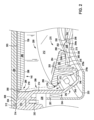
図1は、本原理のある実施形態による基板処理チャンバの高レベルのブロック図を示す。基板処理チャンバ100は、カリフォルニア州サンタクララのアプライドマテリアルズ社から市販されているCLEANW(商標)チャンバを代表するものである。しかしながら、他のプロセスチャンバもまた、本原理と併せて使用することができる。図1の基板処理チャンバ100は、例示的に、プロセスキャビティ108を取り囲むエンクロージャ壁106を備える。壁106は、側壁116、底壁120、および天井124を含む。基板処理チャンバ100は、様々なチャンバ間で基板104を移送するロボットアームなどの基板移送機構によって接続された相互接続されたチャンバのクラスタを有するマルチチャンバプラットフォーム(図示せず)の一部とすることができる。図1に示す実施形態では、基板処理チャンバ100は、例示的に、アルミニウム、銅、タンタル、タンタル窒化物、チタン、チタン窒化物、タングステン、およびタングステン窒化物のうちの1つまたは複数などの材料を基板104上にスパッタ堆積させることができる物理的気相堆積またはPVDチャンバとしても知られているスパッタ堆積チャンバである。
FIG. 1 illustrates a high-level block diagram of a substrate processing chamber according to one embodiment of the present principles. The
基板処理チャンバ100は、基板104を支持するためのペデスタル134を備える基板支持体130を備える。ペデスタル134は、オーバーヘッドスパッタリングターゲット140のスパッタリング表面139に実質的に平行な平面を有する基板受け面138を有する。ペデスタル134の基板受け面138は、処理中に基板104を受けて、支持する。ペデスタル134は、静電チャック、または電気抵抗ヒータもしくは熱交換器などのヒータを含むことができる。動作において、基板104は、基板処理チャンバ100の側壁116の基板装填入り口142を通して基板処理チャンバ100内に導入され、基板支持体130上に配置される。支持体130は、支持体リフトベローズによって昇降可能であり、ロボットアームによって基板104を基板支持体130上に配置する間に、リフトフィンガアセンブリを使用して、基板104を支持体130上に昇降させることができる。ペデスタル134は、プラズマ動作中に電気的に浮遊電位に維持されてもよく、または接地されてもよい。
The
図2は、本原理のある実施形態によるプロセスキット200を含む図1の基板処理チャンバ100の斜視図を示す。図1および図2を相互に参照すると、スパッタリングターゲット140は、バッキング板284に取り付けられたスパッタリング板280を含む。スパッタリング板280は、基板104上にスパッタされる材料を含む。スパッタリング板280は、基板104の平面に平行な平面を形成するスパッタリング表面139を有する中央円筒形メサ286を含むことができる。環状傾斜リム288は、円筒形メサ286を取り囲む。環状リム288は、少なくとも約80度、例えば、約100度~約200度の角度で、円筒形メサ286の平面に対して傾斜させることができる。
2 shows a perspective view of the
環状傾斜リム288、および基板処理チャンバ100内のシールド201の頂壁216に隣接する側壁の複雑な形状は、暗空間領域、すなわち、自由電子が高度に枯渇した、真空としてモデル化することができる領域を含む渦巻き状の間隙300形成する。暗空間領域は、プラズマの侵入、アーク放電、不安定性を防止するように制御される。間隙300の形状は、間隙300を通るスパッタされたプラズマ核種の通路を妨げる迷路として作用し、したがって、スパッタされた堆積物の周辺ターゲット領域の表面への蓄積を低減させる。
The annular
バッキング板284は、スパッタリング板280を支持するための支持表面303と、スパッタリング板280の半径を超えて延在する周辺レッジ304と、を有する。バッキング板284の周辺レッジ304は、基板処理チャンバ100内のアイソレータ310上に戴置された外側フーチング308を備える。周辺レッジ304は、真空シールを形成するためにOリング314が配置されたOリング溝312を含む。アイソレータ310は、バッキング板284を基板処理チャンバ100から電気的に絶縁および分離し、典型的には、アルミニウム酸化物などの誘電体または絶縁材料から形成されたリングである。周辺レッジ304は、ターゲット140とアイソレータ310との間の間隙300を通るスパッタされた材料およびプラズマ核種の流れまたは移動を阻止し、間隙300へのスパッタされた堆積物の侵入を妨げるように成形されている。
The
スパッタリングターゲット140は、ターゲット140にバイアス電圧を印加するターゲット電源320に接続されている。ターゲット電源320がターゲット140に電力を供給している間に、ガスエナジャイザー324がスパッタリングガスを励起して、スパッタリングガスのプラズマを形成する。ガスエナジャイザー324は、コイル326を通る電流の印加によって電力が供給されるソースコイル326を備えることができる。形成されたプラズマは、ターゲット140のスパッタリング表面139に激しくぶつかり、衝突し、材料をスパッタリング表面139から引き離して基板104上にスパッタリングする。
The sputtering
基板処理チャンバ100は、ターゲット140のスパッタリングを改善するためにターゲット140の周りの磁場を成形するための磁場発生器330を備えることができる。容量的に生成されたプラズマは、例えば、永久磁石または電磁コイルが、基板処理チャンバ100内で、基板104の平面に対して平行に回転する軸を有する回転磁場を有する磁場を提供することができる磁場発生器330によって増強させることができる。磁場発生器330は、基板処理チャンバ100のターゲット140の近くに磁場を生成して、ターゲット140に隣接する高密度プラズマ領域のイオン密度を増加させて、ターゲット140材料のスパッタリングを改善することができる。磁場は、実質的に非磁性ターゲット140を通って基板処理チャンバ100内に延在する。
The
スパッタリングガスは、ガス供給システム332を介して基板処理チャンバ100内に導入され、ガス供給システム332は、質量流量コントローラなどのガス流量制御バルブ338を有する導管336を介してガス供給334からガスを供給し、設定された流量のガスを通過させる。ガスは、ミキシングマニホールド(図示せず)に供給され、そこでガスが混合されて所望のプロセスガス組成物が形成され、ガス出口を有するガス分配器340に供給されて、ガスを基板処理チャンバ100内に導入する。プロセスガスは、アルゴンまたはキセノンなどの非反応性ガスを含むことができ、このガスがターゲット140に激しくぶつかり、材料をスパッタリングすることができる。プロセスガスは、反応性ガス、例えば、スパッタされた材料と反応して基板104上に層を形成することができる酸素含有ガスおよび窒素含有ガスのうちの1つまたは複数を含むこともできる。次いで、ガスは、ガスエナジャイザー324によって励起されて、プラズマを形成し、スパッタリングターゲット140をスパッタする。使用済みプロセスガスおよび副産物は、排気システム342を通して基板処理チャンバ100から排気される。排気システム342は、使用済みプロセスガスを受け取り、使用済みガスを、基板処理チャンバ100内のガスの圧力を制御するためのスロットルバルブを有する排気導管346に渡す排気口344を備える。排気導管346は、1つまたは複数の排気ポンプ348に接続されている。
Sputtering gas is introduced into the
基板処理チャンバ100は、基板104を処理するために基板処理チャンバ100の構成要素を動作させる命令セットを有するプログラムコードを含むコントローラ350によって制御することができる。例えば、コントローラ350は、基板支持体130および基板移送機構を動作させるための基板位置決め命令セットと、基板処理チャンバ100へのスパッタリングガスの流量を設定するためにガス流量制御バルブを動作させるためのガス流量制御命令セットと、基板処理チャンバ100内の圧力を維持するために排気スロットルバルブを動作させるためのガス圧力制御命令セットと、ガス励起電力レベルを設定するためにガスエナジャイザー324を動作させるためのガスエナジャイザー制御命令セットと、基板処理チャンバ100内のプロセスをモニタするためのプロセスモニタ命令セットと、を含むプログラムコードを含むことができる。
The
図1および図2の実施形態では、プロセスキット200は、シールド201と、基板104の張り出したエッジ206の手前で終端する基板支持体130の周壁204の周りに配置するためのリングアセンブリ202と、を備える。リングアセンブリ202は、堆積リング208およびカバーリング212を含む。堆積リング208は、支持体130を取り囲む環状バンド215を含む。カバーリング212は、堆積リング208を少なくとも部分的に覆う。堆積リング208およびカバーリング212は、互いに協働して、支持体130の周壁204および基板104の張り出したエッジ206上のスパッタ堆積物の形成を低減させる。
1 and 2, the
図2に示し上述したように、堆積リング208は、支持体130の周壁204の周りに延在し、この周壁を取り囲む環状バンド215を備える。環状バンド215は、環状バンド215から横方向に延在し、支持体130の周壁204に対して実質的に平行な内側リップ250を含む。内側リップ250は、基板104の張り出したエッジ206の直下で終端する。内側リップ250は、基板104および基板支持体130の周辺部を取り囲む堆積リング208の内周を画定して、処理中に基板104によって覆われていない基板支持体130の領域を保護する。例えば、内側リップ250は、普通ならば処理環境にさらされる支持体130の周壁204を取り囲み、少なくとも部分的に覆って、周壁204へのスパッタリング堆積物の堆積を低減させるか、または完全に排除さえする。堆積リング208は、支持体130の露出した側面を保護して、励起されたプラズマ核種による浸食を低減させる働きもすることができる。
As shown in FIG. 2 and described above, the
図1および図2に示す実施形態では、堆積リング208の環状バンド215は、環状バンド215の中央部分に沿って延在する半円形突起252を有し、この半円形突起252の両側に半径方向内向きの窪み254a、bがある。半径方向内向きの窪み254aは、カバーリング212から離間して、それらの間に円弧形間隙256を形成し、この円弧形間隙が迷路として作用して、プラズマ核種の円弧形間隙256への侵入を低減させる。開いた内側チャネル258は、内側リップ250と半円形突起252との間に位置する。開いた内側チャネル258は、半径方向内向きに延在して、基板104の張り出したエッジ206の下で少なくとも部分的に終端する。開いた内側チャネル258は、堆積リング208の洗浄中にこれらの部分からのスパッタリング堆積物の除去を容易にする。堆積リング208は、外側に延在し、半円形突起252の半径方向外向きに位置するレッジ260も有する。レッジ260は、カバーリング212を支持するのに役立つ。
In the embodiment shown in FIGS. 1 and 2, the
図2に示し上述したように、カバーリング212は、堆積リング208を取り囲み、堆積リング208を受け入れるように少なくとも部分的に覆い、したがって、スパッタリング堆積物の大部分から堆積リング208を遮る。カバーリング212は、半径方向内向きに傾斜し、基板支持体130を取り囲む傾斜した頂面264を含む環状ウェッジ262を備える。カバーリング212の傾斜した頂面264の角度は、例えば、基板104の張り出したエッジ206に最も近いスパッタ堆積物の蓄積を最小化するように設計されており、そうでなければ、基板104全体にわたって得られる堆積均一性に悪影響を及ぼす。
2 and described above, the
環状ウェッジ262の傾斜した頂面264は、内周266および外周268を有する。内周266は、堆積リング208の開いた内側チャネル258を含む半径方向内向きの窪み254aの上を覆う突出縁部270を含む。突出縁部270は、堆積リング208の開いた内側チャネル258上へのスパッタリング堆積物の堆積を低減させる。突出縁部270は、堆積リング208で形成された円弧状の間隙256の幅の少なくとも約半分に相当する距離突出する。突出縁部270は、円弧状の間隙256と協働し補完して、カバーリング212と堆積リング208との間に、周壁204へのプロセス堆積物の流れを阻止する渦巻き状の狭窄した流路を形成するように、サイズ調整され、成形され、位置決めされている。狭い間隙256の狭窄した流路は、堆積リング208とカバーリング212の合わせ面上での低エネルギースパッタ堆積物の蓄積を制限しており、そうでなければ、堆積物を互いに、または基板104の周囲の張り出したエッジ206に付着させることになる。
The sloped
傾斜した頂面264の外周268の周りには、球状突起272がある。図2の実施形態では、球状突起272は、シールド201とともに円弧状の間隙を形成する楕円形の円周面274を含む。
Around the
カバーリング212は、環状ウェッジ262の傾斜した頂面264から下向きに延在して、堆積リング208のレッジ260上に戴置されるフーチング276を備える。フーチング276は、ウェッジ262から下向きに延在して、堆積リング208を実質的に亀裂または破断させることなく、堆積リング208を押圧する。カバーリング212は、環状ウェッジ262から下向きに延在し、間に間隙を有する内側および外側の円筒形バンド278a、bをさらに備える。一部の実施形態では、内側および外側の円筒形バンド278a、bは、実質的に垂直である。円筒形バンド278a、bは、ウェッジ262のフーチング276の半径方向外向きに位置する。内側円筒形バンド278aは、外側円筒形バンド278bよりも高さが低い。
The
カバーリング212は、調整可能とすることができ、シールド201のガスコンダクタンス孔249を異なる高さの範囲で効果的にシールドする。例えば、カバーリング212は、チャンバ内の基板支持体130との関係でカバーリング212の高さを調整するために上げ下げすることができる。
The
図2に示すように、プロセスキット200のシールド201は、基板支持体130に面するスパッタリングターゲット140のスパッタリング表面139、および基板支持体130の外周を取り囲む。シールド201は、基板処理チャンバ100の側壁116を覆い、かつ遮って、スパッタリングターゲット140のスパッタリング表面139に由来するスパッタリング堆積物がシールド201の背後の構成要素および表面上に堆積するのを低減させる。例えば、シールド201は、支持体130の表面、基板104の張り出したエッジ206、基板処理チャンバ100の側壁116および底壁120を保護することができる。
2, the
図2に示す実施形態では、シールド201は、スパッタリングターゲット140のスパッタリング表面139および基板支持体130を取り囲むようにサイズ調整された直径を有する円筒形バンド214を含む。円筒形バンド214は、スパッタリングターゲット140のスパッタリング表面139を取り囲む頂壁216を有する。シールド201の環状アダプタ226は、基板処理チャンバ100の側壁116を取り囲む。複数のピン230は、アダプタ226に沿って円形または円形の配置に沿って離間して配置されている。一部の実施形態では、少なくとも3つのピン230が、アダプタ226上で円形に配置されている。各ピン230は、例えば鋼、または例えばステンレス鋼などの材料から構成された剛性部材を含むことができる。
In the embodiment shown in FIG. 2, the
シールド201は、基板支持体130を取り囲む底壁242を備える。傾斜壁244は、円筒形バンド214の底壁242から内向きに延在し、基板支持体130を取り囲む。図2に示す実施形態では、傾斜壁244は、実質的に直線のプロファイルを含む。すなわち、本発明者らは、傾斜壁244が、シールドの下方部分に傾斜した段差を含むBKMプロセスチャンバと比較して、実質的に直線のプロファイルを含む場合、シールド201上に堆積するスパッタ材料の剥離が低減されると判断した。したがって、傾斜壁244を傾斜した段差と比較してより直線的にすることにより、シールド201上に堆積したスパッタされた材料の剥離が低減される。
The
シールド201の傾斜壁244は、プロセスガスを通過させることができる少なくとも1つのガスコンダクタンス孔249を有するチャネル246の外側区間を形成する。チャネル246は、傾斜壁244から離間された内側の第2の区間253も備える。シールド201により、基板処理チャンバ100からのガスがガスコンダクタンス孔249を通過し、チャネル246を通って循環し、プロセスキャビティ108(例えば、処理容積)に入るのが可能になる。図2に示す実施形態では、傾斜壁244のガスコンダクタンス孔249は実質的に矩形状であるが、本原理による他の実施形態では、傾斜壁244のガスコンダクタンス孔は実質的に任意の形状に従うことができる。加えて、図2に示す実施形態では、ガスコンダクタンス孔249は、例示的に傾斜壁244の中央部分に位置しているが、代替の実施形態では、ガスコンダクタンス孔249は、カバーリング212が、シールド201のガスコンダクタンス孔249を通過するガスが間隙300への直接の見通し線を有するのを防止することができる限り、傾斜壁244に沿った実質的に任意の場所に位置することができる。例えば、一部の実施形態では、ガスコンダクタンス孔249は、傾斜壁244の下方部分に位置することができる。
The
本原理の実施形態によると、カバーリング212の球状突起272、シールド201の傾斜壁244の角度および長さ、ならびにシールド201上のガスコンダクタンス孔249のサイズ、形状、および位置は、プロセスキット構成要素上に堆積したスパッタ材料の剥離を低減させ、見通し線堆積物がプロセスキャビティ108を出てチャンバ本体キャビティ(例えば、非処理容積)に入るのを遮断するように設計され、協働する。より具体的には、カバーリング212の球状突起272、シールド201の傾斜壁244の角度および長さ、ならびにシールド201上のガスコンダクタンス孔249の形状および位置は、プロセスキット構成要素上のスパッタ堆積物の剥離を低減させ、シールド201のガスコンダクタンス孔249を通過するガスがターゲット140とアイソレータ310との間の間隙300への直接の見通し線を有すること防止するように設計され、プラズマをプロセスキャビティ108内に閉じ込め、そのためプラズマによって運ばれたスパッタ堆積物が間隙300に入るのを防止する。
According to an embodiment of the present principles, the
本発明者らは、傾斜壁244が実質的に直線のプロファイルを含む場合、シールド201上に堆積したスパッタ材料の剥離が低減すると判断した。より具体的には、シールド201の下方部分の傾斜壁244を実質的に直線にすることにより、結果として、スパッタ堆積物のシールド201上への膜接着が良好になり、スパッタ堆積物の剥離が少なくなる。本発明者らは、カバーリング212の突起272がシールド201のガスコンダクタンス孔249と、ターゲット140とアイソレータ310間の間隙300との間の見通し線を遮断することができるように傾斜壁244に角度を付ける必要があるとさらに判断した。加えて、傾斜壁244の長さは、シールド201のガスコンダクタンス孔249と、ターゲット140とアイソレータ310間の間隙300との間の見通し線を、カバーリング212の突起272によって遮断することができるように、ガスコンダクタンス孔249が傾斜壁244上に位置することができるような長さでなければならない。本発明の原理による一部の実施形態では、ガスコンダクタンス孔249は、BKMプロセスキットのガスコンダクタンスよりも典型的には低い位置でシールド201の傾斜壁244上に位置し、そのためガスコンダクタンス孔249は、カバーリング212のより近くに位置する。一実施形態では、本原理によるプロセスキットは、幅が約0.45インチ、例えば約0.2インチ~約0.8インチ、長さが約1.6インチ、例えば約1インチ~約2インチのコンダクタンス孔249を有するシールド201を含む。シールド201は、約25度、例えば約15度~約45度の角度を有する傾斜壁244をさらに含むことができる。そのような構成により、本原理によるプロセスキット200は、結果としてシールド201からのスパッタ堆積物の剥離を少なくする。加えて、シールド201のガスコンダクタンス孔249と、ターゲット140とアイソレータ310間の間隙300との間の見通し線は、カバーリング212の球状突起272によって遮断され、プラズマによって運ばれるスパッタ堆積物が間隙300に入るのを防止する。
The inventors have determined that spalling of sputtered material deposited on the
図2において、ターゲット140とアイソレータ310との間の間隙300に始まり、カバーリング212の突起272に向かって延在する点線299は、シールド201のガスコンダクタンス孔249と間隙300との間の見通し線を表す。図2に示すように、カバーリング212の球状突起272、シールド201の傾斜壁244の角度および長さ、ならびにシールド201上のガスコンダクタンス孔249は、シールド201のガスコンダクタンス孔249と、ターゲット140とアイソレータ310間の間隙300との間の見通し線を遮断し、少なくともシールド201上のスパッタ堆積物の剥離を低減させるように、互いに関係して成形され、配置されている。
In FIG. 2, the dotted
本原理によるプロセスキット200では、ガスコンダクタンス孔249は、シールド201およびシールド201の傾斜壁244の下方に位置し、コンダクタンス孔が円筒形バンド214の表面に平行で、シールドの上方に位置する最もよく知られた方法(BKM)のプロセスキットとは異なる。本原理によるプロセスキット200の形状寸法は、プラズマを閉じ込めるために、プロセスキット200のライナー203がさらに内向きに延在することを必要とする。すなわち、図2に戻って参照すると、プロセスキット200は、ライナー203をさらに備えることができる。図2のライナー203は、例示的に、アダプタ226とシールド201との間に位置し、シールド201の基部のレベルまで延在し、BKMプロセスキットと比較して内向きに移動して、シールド201の底部の傾斜壁244上に位置する、BKMプロセスキットと比較してカバーリング212に相対的に近いシールド201のガスコンダクタンス孔249を遮る。
In the
シールド接地ユニットを備えるプロセスチャンバでは、本発明の原理に従って、シールド接地ユニットをより小さくして、プロセスキットのライナーを内向きに移動させることができる。図4は、本原理の代替の実施形態によるプロセスキット400を含む図1の基板処理チャンバ100の斜視図を示す。図4の基板処理チャンバ100は、プロセスキット400、ライナー203、およびシールド接地ユニット402を含む。図4のプロセスキット400は、シールド201、カバーリング212、および堆積リング208を備える。図4に示すように、シールド接地ユニット402は、シールド201の下に位置し、シールド201を接地するように実装されている。図4に示すシールド接地ユニット402は、プロセスキット400のライナー203を内向きに移動させて、プラズマを効果的に閉じ込めることができるようにサイズが縮小されている。図4のシールド接地ユニット404の点線部分406は、シールド201のガスコンダクタンス孔249を遮り、プラズマを閉じ込めるために、シールド201に対してライナー203の配置を適応させるように除去されたシールド接地ユニット404の部分を表す。
In a process chamber with a shield ground unit, the shield ground unit can be made smaller to move the liner of the process kit inward in accordance with the principles of the present invention. FIG. 4 shows a perspective view of the
図4に示すように、シールド接地ユニット404のサイズが縮小しているため、シールド201は、シールド接地ユニット402にわずかしか接触しない。そのため、図4の実施形態では、シールド201の内側の第2の区間253は、例示的に、シールド接地ユニット402と接触するためのフランジ404を備える。上述したように、サイズを縮小させたシールド接地ユニット402は、シールド201のコンダクタンス孔249を適切に遮り、プラズマを閉じ込めるために、ライナー203を内向きに移動させることができる。
As shown in FIG. 4, due to the reduced size of the
本原理による一部の実施形態では、プロセスチャンバ内のガスコンダクタンスは、カバーリング212の少なくとも球状突起272、シールド201の傾斜壁244の角度および長さ、ならびにシールド201上のガスコンダクタンス孔249を互いに関連させて成形および配置する際に考慮に入れられる。より具体的には、図1の基板処理チャンバ100などの基板処理チャンバでは、必要なプロセスガスをプロセスキャビティに供給し、使用済みプロセスガスを適切に排気するために、高コンダクタンスのガス流路が必要である。本原理による一部の実施形態では、カバーリング212の球状突起272、シールド201の傾斜壁244の角度および長さ、ならびにシールド201上のガスコンダクタンス孔249を互いに関連させて成形および配置して、シールド201のガスコンダクタンス孔249とターゲット140とアイソレータ310間の間隙300との間の見通し線を遮断し、スパッタ堆積物の剥離を低減させることに加えて、カバーリング212の球状突起272、シールド201の傾斜壁244の角度および長さ、ならびにシールド201上のガスコンダクタンス孔249を、さらに成形および配置して、基板処理チャンバ100内のガスコンダクタンスを最大化させるように、または最もよく知られている方法(BKM)のガスコンダクタンスと少なくとも一致させるように試みる。
In some embodiments according to the present principles, the gas conductance in the process chamber is taken into consideration when shaping and positioning at least the
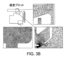
図3Aは、コンピュータ支援エンジニアリング(CAE)分析を使用して生成されたBKM基板処理チャンバのガス流速のプロットを示す。図3Bは、CAE分析を使用して生成された、図1の基板処理チャンバ100などの本原理による基板処理チャンバのガス流速のプロットを示す。図3Aと図3Bのプロットの比較から判断することができるように、本原理による処理チャンバのガスコンダクタンスの最大速度は、BKM処理チャンバと一致している。図3Aと図3Bのプロットの比較は、図1の基板処理チャンバ100のシールド201の傾斜壁244におけるガスコンダクタンス孔249の周りのガスの速度が、BKM基板処理チャンバのガスコンダクタンススロット周辺のガスの速度よりも低いことをさらに示す。そのため、本原理による基板処理チャンバ100内の基板の表面上の粒子付着物は、少なくとも、より低速のガスにより、プロセスキャビティ108の表面上のスパッタ堆積物の剥離が少なくなり、より低速のガスにより、はがれたスパッタ粒子を運ぶことが少なくなるため、少なくなる。
3A shows a plot of gas flow rates for a BKM substrate processing chamber generated using computer-aided engineering (CAE) analysis. FIG. 3B shows a plot of gas flow rates for a substrate processing chamber according to present principles, such as the
本原理による一部の実施形態では、シールド201、堆積リング208、およびカバーリング212のうちの少なくとも1つの露出表面は、コーティングで処理されて、基板処理中に露出表面上に堆積させた膜の粒子保持を改善する。コーティングは、一般に、露出表面にミクロまたはマクロのテクスチャリングを提供する突起を含む。一実施形態では、コーティングは、カリフォルニア州サンタクララのアプライドマテリアルズ社から入手可能なLavaCoatまたはLavaCoatIIコーティングを含むことができる。一部の実施形態では、コーティングは、丸みを帯びた粒子、半円形の突起を含むことができ、ならびに/または他の形状および形状寸法を含むことができる。コーティングの突起は、隣接する突起から分離した離散的な突起を含むことができる。代替としてまたは加えて、コーティングの表面テクスチャリングは、粒子接着を改善するために波形プロファイルを含むことができる。コーティングの波形プロファイルは、エッチング、ビーズもしくはグリット、ブラスト、レーザアブレーション、または3D印刷によって形成することができる。一部の実施形態では、コーティングは、基板処理チャンバ100およびプロセスキット200の露出表面全体に塗布することができ、または代替として基板処理チャンバ100およびプロセスキット200の露出表面の一部のみに塗布することができる。一部の他の実施形態では、基板処理チャンバ100の構成要素のいずれかの露出表面は、コーティングで処理されて、上述したように、基板処理中に露出表面に堆積させた膜の粒子保持を改善する。
In some embodiments according to the present principles, the exposed surface of at least one of the
本発明者らは、上述したような、本原理によるプロセスキットに対してモル分率分析試験を行って、反応性ガスを用いたプロセス条件がBKMプロセスキットとどれだけよく一致するかを判定した。プロセスキャビティの領域を綿密に調べると、いくつかの相違が認められたが、本原理によるプロセスキットの反応性ガスを用いたプロセス条件は、マクロレベルでよく一致している。 The inventors performed mole fraction analysis testing on the process kit according to the present principles, as described above, to determine how well the reactive gas process conditions matched the BKM process kit. Although close inspection of the process cavity area revealed some differences, the reactive gas process conditions of the process kit according to the present principles matched well at a macro level.
上述したプロセスキット200は、基板処理チャンバ100のプロセスサイクル数および処理時間を大幅に増加させ、洗浄間の時間量を増加させる。このような利点は、基板104の周囲の構成要素上に形成されるスパッタリング堆積物の剥離の量を減らすこと、およびターゲット140とアイソレータ310との間の間隙300に向かってガスによって運ばれるスパッタリング堆積物の量を減らすことによって達成される。
The
前述の事項は、本原理の実施形態を対象としているが、他のおよびさらなる実施形態が、その基本的な範囲から逸脱することなく考案され得る。例えば、プロセスキット200またはその構成要素は、当業者には明らかなように、他のタイプの用途、例えば、エッチング、CVD、およびエッチングチャンバで使用することができる。したがって、添付の特許請求の範囲の精神および範囲は、本明細書に含まれる実施形態の説明に限定されるべきではない。
While the foregoing is directed to embodiments of the present principles, other and further embodiments may be devised without departing from the basic scope thereof. For example, the
Claims (10)
前記スパッタリングターゲットを取り囲むように構成された頂壁および前記基板支持体を取り囲むように構成された底壁を有する円筒形バンドと、
前記円筒形バンドの前記底壁から下向きかつ半径方向内向きに延在する傾斜壁であり、実質的に直線のプロファイルを有する、傾斜壁と、
プロセスガスを通過させることができるように前記傾斜壁の下方部分に位置する少なくとも1つのガス孔と、
を備え、
前記少なくとも1つのガス孔は、前記傾斜壁の下方部分に配置され、プロセスガスがそこを通過できるようにし、前記カバーリングの前記球状突起が、前記基板処理チャンバに取り付けられると、前記カバーリングの前記球状突起が、前記シールド上の前記少なくとも1つのガス孔と前記基板処理チャンバのチャンバ本体キャビティへの入り口との間の見通し線を遮断するように、前記少なくとも1つのガス孔は、前記傾斜壁の下方部分に配置され、
前記カバーリングの前記球状突起によって前記見通し線を遮断することで、プラズマによって運ばれる前記スパッタ堆積物が前記チャンバ本体キャビティに入るのを防止し、
前記傾斜壁の前記少なくとも1つのガス孔が、約0.2インチ~約0.8インチの幅、および約1インチ~2インチの長さを含み、
前記傾斜壁が約15度~45度の角度を含む、プロセスキットシールド。 1. A process kit shield configured to surround a sputtering target facing a substrate support in a substrate processing chamber including a cover ring disposed about the substrate support, the cover ring including an annular wedge about the substrate support including a sloped top surface, the sloped top surface having an inner periphery and an outer periphery, the sloped top surface having a spherical protrusion on the outer periphery, the process kit shield comprising:
a cylindrical band having a top wall configured to surround the sputtering target and a bottom wall configured to surround the substrate support;
a sloped wall extending downwardly and radially inwardly from the bottom wall of the cylindrical band, the sloped wall having a substantially straight profile;
at least one gas hole located in a lower portion of said inclined wall for allowing a process gas to pass therethrough;
Equipped with
the at least one gas hole is disposed in a lower portion of the sloped wall to allow process gas to pass therethrough, the at least one gas hole being disposed in a lower portion of the sloped wall such that, when the spherical protrusion of the cover ring is attached to the substrate processing chamber , the spherical protrusion of the cover ring blocks a line of sight between the at least one gas hole on the shield and an entrance to a chamber body cavity of the substrate processing chamber ;
blocking the line of sight with the spherical protrusion of the cover ring to prevent the sputter deposits carried by the plasma from entering the chamber body cavity ;
the at least one gas hole in the angled wall comprises a width of about 0.2 inches to about 0.8 inches and a length of about 1 inch to 2 inches;
The process kit shield, wherein the angled wall comprises an angle of about 15 degrees to 45 degrees .
前記スパッタリングターゲットを取り囲むように構成されたシールドであり、
前記スパッタリングターゲットを取り囲むように構成された頂壁および前記基板支持体を取り囲むように構成された底壁を有する円筒形バンド、
前記円筒形バンドの前記底壁から下向きかつ半径方向内向きに延在する傾斜壁で、実質的に直線のプロファイルを有する、傾斜壁、および
プロセスガスを通過させることができるように前記傾斜壁の下方部分に位置する少なくとも1つのガス孔、
を備える、シールドと、
リングアセンブリであり、
前記基板支持体を取り囲むように構成されたカバーリングで、前記基板支持体の周りに傾斜した頂面を含む環状ウェッジを備え、前記傾斜した頂面が内周および外周を有するカバーリング、前記傾斜した頂面の外周の周りの球状突起、前記傾斜した頂面から下向きに延在するフーチング、前記傾斜した頂面の内周の周りの突出縁部、および前記環状ウェッジから下向きに延在する内側および外側の円筒形バンド、
を備える、リングアセンブリと、
を備え、
前記少なくとも1つのガス孔は、前記傾斜壁の下方部分に配置され、プロセスガスがそこを通過できるようにし、前記カバーリングの前記球状突起が、前記基板処理チャンバに取り付けられると、前記カバーリングの前記球状突起が、前記少なくとも1つのガス孔と前記基板処理チャンバのチャンバ本体キャビティへの入り口との間の見通し線を遮断するように、前記傾斜壁の下方部分に配置され、
前記カバーリングの前記球状突起によって前記見通し線を遮断することで、プラズマによって運ばれる前記スパッタ堆積物が前記チャンバ本体キャビティに入るのを防止し、
前記シールドの前記傾斜壁の下方部分の前記少なくとも1つのガス孔が、約0.2インチ~約0.8インチの幅、および約1インチ~2インチの長さを含み、
前記シールドの前記傾斜壁が、約15度~45度の角度を含む、プロセスキット。 1. A process kit configured for placement around a sputtering target and a substrate support in a substrate processing chamber, comprising:
a shield configured to surround the sputtering target;
a cylindrical band having a top wall configured to surround the sputtering target and a bottom wall configured to surround the substrate support;
a sloping wall extending downwardly and radially inwardly from the bottom wall of the cylindrical band, the sloping wall having a substantially linear profile; and at least one gas hole located in a lower portion of the sloping wall to allow a process gas to pass therethrough.
a shield;
A ring assembly,
a cover ring configured to surround the substrate support, the cover ring comprising an annular wedge including a sloped top surface around the substrate support, the sloped top surface having an inner periphery and an outer periphery; a spherical protrusion around the outer periphery of the sloped top surface; a footing extending downwardly from the sloped top surface; a protruding lip around an inner periphery of the sloped top surface; and inner and outer cylindrical bands extending downwardly from the annular wedge;
a ring assembly comprising:
Equipped with
the at least one gas hole is disposed in a lower portion of the sloped wall to allow process gas to pass therethrough, and the spherical protrusion of the cover ring is disposed in a lower portion of the sloped wall such that, when the spherical protrusion of the cover ring is attached to the substrate processing chamber, the spherical protrusion of the cover ring blocks a line of sight between the at least one gas hole and an entrance to a chamber body cavity of the substrate processing chamber;
blocking the line of sight with the spherical protrusion of the cover ring to prevent the sputter deposits carried by the plasma from entering the chamber body cavity ;
the at least one gas hole in the lower portion of the angled wall of the shield comprises a width of about 0.2 inches to about 0.8 inches and a length of about 1 inch to 2 inches;
The process kit, wherein the angled wall of the shield comprises an angle of between about 15 degrees and 45 degrees .
前記プロセスキャビティ内に配置された基板支持体と、
前記プロセスキャビティ内で前記基板支持体の反対側に配置されたスパッタリングターゲットと、
前記基板支持体および前記スパッタリングターゲットの周り配置されたプロセスキットと、
を備える、基板を処理するためのスパッタリング装置であって、前記プロセスキットが、
前記スパッタリングターゲットを取り囲むシールドであり、
前記スパッタリングターゲットを取り囲む頂壁および前記基板支持体を取り囲む底壁を有する円筒形バンド、
前記円筒形バンドの前記底壁から半径方向内向きに延在する傾斜壁で、実質的に直線のプロファイルを有する傾斜壁、および
プロセスガスを通過させることができるように前記傾斜壁の下方部分に位置する少なくとも1つのガス孔
を備える、シールド
ならびに
リングアセンブリであり、
前記基板支持体の周りに位置するカバーリングで、
前記基板支持体の周りに傾斜した頂面を含む環状ウェッジで、前記傾斜した頂面が内周および外周を有する、環状ウェッジ、
前記傾斜した頂面の外周の周りの球状突起、
前記傾斜した頂面から下向きに延在するフーチング、
前記傾斜した頂面の内周の周りの突出縁部、および
前記環状ウェッジから下向きに延在する内側および外側の円筒形バンド、
を備える、カバーリング
を備える、リングアセンブリ
を備え、
前記カバーリングの前記球状突起が、前記シールド上の前記少なくとも1つのガス孔と前記プロセスチャンバの前記チャンバ本体キャビティへの入り口との間の見通し線を遮断するように、前記少なくとも1つのガス孔は、前記傾斜壁の下方部分に位置し、
前記カバーリングの前記球状突起によって前記見通し線を遮断することで、プラズマによって運ばれる前記スパッタ堆積物が前記チャンバ本体キャビティに入るのを防止し、
前記傾斜壁の前記少なくとも1つのガス孔が、約0.2インチ~約0.8インチの幅、および約1インチ~2インチの長さを含み、
前記傾斜壁が約15度~45度の角度を含む、装置。 a process chamber having a process cavity and a chamber body cavity;
a substrate support disposed within the process cavity;
a sputtering target disposed within the process cavity opposite the substrate support;
a process kit disposed around the substrate support and the sputtering target;
1. A sputtering apparatus for processing a substrate, comprising:
a shield surrounding the sputtering target;
a cylindrical band having a top wall surrounding said sputtering target and a bottom wall surrounding said substrate support;
a sloping wall extending radially inward from the bottom wall of the cylindrical band, the sloping wall having a substantially straight profile; and at least one gas hole located in a lower portion of the sloping wall to allow a process gas to pass therethrough; and a ring assembly,
a cover ring positioned around the substrate support;
an annular wedge including a sloped top surface about said substrate support, said sloped top surface having an inner periphery and an outer periphery;
a spherical protrusion around the periphery of said inclined top surface;
a footing extending downwardly from said sloping top surface;
a protruding edge around an inner periphery of said sloped top surface; and inner and outer cylindrical bands extending downwardly from said annular wedge.
comprising a cover ring; comprising a ring assembly;
the at least one gas hole is located in a lower portion of the sloped wall such that the spherical protrusion of the cover ring blocks a line of sight between the at least one gas hole on the shield and an entrance to the chamber body cavity of the process chamber ;
blocking the line of sight with the spherical protrusion of the cover ring to prevent the sputter deposits carried by the plasma from entering the chamber body cavity ;
the at least one gas hole in the angled wall comprises a width of about 0.2 inches to about 0.8 inches and a length of about 1 inch to 2 inches;
The apparatus , wherein the angled wall comprises an angle of about 15 degrees to 45 degrees .
Applications Claiming Priority (3)
| Application Number | Priority Date | Filing Date | Title |
|---|---|---|---|
| US201862623081P | 2018-01-29 | 2018-01-29 | |
| US62/623,081 | 2018-01-29 | ||
| PCT/US2019/014207 WO2019147493A1 (en) | 2018-01-29 | 2019-01-18 | Process kit geometry for particle reduction in pvd processes |
Publications (3)
| Publication Number | Publication Date |
|---|---|
| JP2021511443A JP2021511443A (en) | 2021-05-06 |
| JPWO2019147493A5 JPWO2019147493A5 (en) | 2022-01-26 |
| JP7466460B2 true JP7466460B2 (en) | 2024-04-12 |
Family
ID=67393674
Family Applications (1)
| Application Number | Title | Priority Date | Filing Date |
|---|---|---|---|
| JP2020562069A Active JP7466460B2 (en) | 2018-01-29 | 2019-01-18 | Process kit geometries for particle reduction in PVD processes - Patents.com |
Country Status (6)
| Country | Link |
|---|---|
| US (1) | US11935732B2 (en) |
| JP (1) | JP7466460B2 (en) |
| KR (1) | KR20200105955A (en) |
| CN (1) | CN111602235A (en) |
| TW (1) | TWI808120B (en) |
| WO (1) | WO2019147493A1 (en) |
Families Citing this family (4)
| Publication number | Priority date | Publication date | Assignee | Title |
|---|---|---|---|---|
| CN112011759B (en) * | 2020-08-24 | 2022-06-21 | 宁波中骏森驰汽车零部件股份有限公司 | PVD vacuum coating machine |
| CN113445017B (en) * | 2021-06-01 | 2022-12-09 | 北京北方华创微电子装备有限公司 | Semiconductor chamber and semiconductor processing equipment |
| CN115747733A (en) * | 2022-11-25 | 2023-03-07 | 宁波江丰电子材料股份有限公司 | Deposition ring for sputtering and application thereof |
| CN116288182A (en) * | 2022-11-25 | 2023-06-23 | 宁波江丰电子材料股份有限公司 | Protective ring for sputtering and application thereof |
Citations (3)
| Publication number | Priority date | Publication date | Assignee | Title |
|---|---|---|---|---|
| JP2007277649A (en) | 2006-04-07 | 2007-10-25 | Nec Electronics Corp | Vacuum treatment apparatus |
| JP2008261047A (en) | 2007-01-29 | 2008-10-30 | Applied Materials Inc | Treatment kit for substrate treatment chamber |
| JP2010163690A5 (en) | 2010-03-02 | 2011-05-26 |
Family Cites Families (12)
| Publication number | Priority date | Publication date | Assignee | Title |
|---|---|---|---|---|
| US6673198B1 (en) | 1999-12-22 | 2004-01-06 | Lam Research Corporation | Semiconductor processing equipment having improved process drift control |
| EP1524682B1 (en) * | 2003-10-17 | 2011-10-05 | Tosoh Corporation | Component for vacuum apparatus, production method thereof and apparatus using the same |
| US8435379B2 (en) | 2007-05-08 | 2013-05-07 | Applied Materials, Inc. | Substrate cleaning chamber and cleaning and conditioning methods |
| KR101939640B1 (en) | 2008-04-16 | 2019-01-17 | 어플라이드 머티어리얼스, 인코포레이티드 | Wafer processing deposition shielding components |
| JP4580040B2 (en) | 2008-07-31 | 2010-11-10 | キヤノンアネルバ株式会社 | Plasma processing apparatus and electronic device manufacturing method |
| US9834840B2 (en) | 2010-05-14 | 2017-12-05 | Applied Materials, Inc. | Process kit shield for improved particle reduction |
| US8647485B2 (en) | 2012-03-30 | 2014-02-11 | Applied Materials, Inc. | Process kit shield for plasma enhanced processing chamber |
| US20130277203A1 (en) | 2012-04-24 | 2013-10-24 | Applied Materials, Inc. | Process kit shield and physical vapor deposition chamber having same |
| US10546733B2 (en) | 2014-12-31 | 2020-01-28 | Applied Materials, Inc. | One-piece process kit shield |
| US9953812B2 (en) | 2015-10-06 | 2018-04-24 | Applied Materials, Inc. | Integrated process kit for a substrate processing chamber |
| WO2017091334A1 (en) | 2015-11-24 | 2017-06-01 | Applied Materials, Inc. | Pre-coated shield for use in vhf-rf pvd chambers |
| US11114289B2 (en) | 2016-04-27 | 2021-09-07 | Applied Materials, Inc. | Non-disappearing anode for use with dielectric deposition |
-
2019
- 2019-01-18 KR KR1020207024374A patent/KR20200105955A/en not_active Application Discontinuation
- 2019-01-18 CN CN201980008457.8A patent/CN111602235A/en active Pending
- 2019-01-18 JP JP2020562069A patent/JP7466460B2/en active Active
- 2019-01-18 WO PCT/US2019/014207 patent/WO2019147493A1/en active Application Filing
- 2019-01-18 US US16/251,716 patent/US11935732B2/en active Active
- 2019-01-28 TW TW108103042A patent/TWI808120B/en active
Patent Citations (3)
| Publication number | Priority date | Publication date | Assignee | Title |
|---|---|---|---|---|
| JP2007277649A (en) | 2006-04-07 | 2007-10-25 | Nec Electronics Corp | Vacuum treatment apparatus |
| JP2008261047A (en) | 2007-01-29 | 2008-10-30 | Applied Materials Inc | Treatment kit for substrate treatment chamber |
| JP2010163690A5 (en) | 2010-03-02 | 2011-05-26 |
Also Published As
| Publication number | Publication date |
|---|---|
| TWI808120B (en) | 2023-07-11 |
| US20190237311A1 (en) | 2019-08-01 |
| WO2019147493A1 (en) | 2019-08-01 |
| TW201932630A (en) | 2019-08-16 |
| CN111602235A (en) | 2020-08-28 |
| JP2021511443A (en) | 2021-05-06 |
| US11935732B2 (en) | 2024-03-19 |
| KR20200105955A (en) | 2020-09-09 |
Similar Documents
| Publication | Publication Date | Title |
|---|---|---|
| JP7466460B2 (en) | Process kit geometries for particle reduction in PVD processes - Patents.com | |
| JP5563197B2 (en) | Substrate processing chamber processing kit | |
| CN109585251B (en) | One-piece process kit shield | |
| CN108028184B (en) | One-piece process kit shield for reducing electric field effects near a substrate | |
| JP7402253B2 (en) | Physical vapor deposition (PVD) chamber with in-situ chamber cleaning capability | |
| JP5611350B2 (en) | Process kit for RF physical vapor deposition | |
| US8668815B2 (en) | Process kit for RF physical vapor deposition | |
| WO2017007729A1 (en) | Process kit having tall deposition ring and deposition ring clamp | |
| KR20100017278A (en) | Cooling shield for substrate processing chamber | |
| US11961723B2 (en) | Process kit having tall deposition ring for PVD chamber | |
| US11339466B2 (en) | Heated shield for physical vapor deposition chamber | |
| WO2017044791A1 (en) | One-piece process kit shield for reducing the impact of an electric field near the substrate | |
| US11581167B2 (en) | Process kit having tall deposition ring and smaller diameter electrostatic chuck (ESC) for PVD chamber | |
| US20240093355A1 (en) | Glassy Carbon Shutter Disk For Physical Vapor Deposition (PVD) Chamber | |
| KR20240046791A (en) | Shutter disks for physical vapor deposition (PVD) chambers |
Legal Events
| Date | Code | Title | Description |
|---|---|---|---|
| A521 | Request for written amendment filed |
Free format text: JAPANESE INTERMEDIATE CODE: A523 Effective date: 20220118 |
|
| A621 | Written request for application examination |
Free format text: JAPANESE INTERMEDIATE CODE: A621 Effective date: 20220118 |
|
| A977 | Report on retrieval |
Free format text: JAPANESE INTERMEDIATE CODE: A971007 Effective date: 20221226 |
|
| A131 | Notification of reasons for refusal |
Free format text: JAPANESE INTERMEDIATE CODE: A131 Effective date: 20230105 |
|
| A521 | Request for written amendment filed |
Free format text: JAPANESE INTERMEDIATE CODE: A523 Effective date: 20230405 |
|
| A131 | Notification of reasons for refusal |
Free format text: JAPANESE INTERMEDIATE CODE: A131 Effective date: 20230718 |
|
| A601 | Written request for extension of time |
Free format text: JAPANESE INTERMEDIATE CODE: A601 Effective date: 20231018 |
|
| A521 | Request for written amendment filed |
Free format text: JAPANESE INTERMEDIATE CODE: A523 Effective date: 20231215 |
|
| TRDD | Decision of grant or rejection written | ||
| A01 | Written decision to grant a patent or to grant a registration (utility model) |
Free format text: JAPANESE INTERMEDIATE CODE: A01 Effective date: 20240304 |
|
| A61 | First payment of annual fees (during grant procedure) |
Free format text: JAPANESE INTERMEDIATE CODE: A61 Effective date: 20240402 |
|
| R150 | Certificate of patent or registration of utility model |
Ref document number: 7466460 Country of ref document: JP Free format text: JAPANESE INTERMEDIATE CODE: R150 |