JP7450607B2 - Coil and its manufacturing method - Google Patents
Coil and its manufacturing method Download PDFInfo
- Publication number
- JP7450607B2 JP7450607B2 JP2021510725A JP2021510725A JP7450607B2 JP 7450607 B2 JP7450607 B2 JP 7450607B2 JP 2021510725 A JP2021510725 A JP 2021510725A JP 2021510725 A JP2021510725 A JP 2021510725A JP 7450607 B2 JP7450607 B2 JP 7450607B2
- Authority
- JP
- Japan
- Prior art keywords
- layer
- coil
- region
- multilayer film
- along
- Prior art date
- Legal status (The legal status is an assumption and is not a legal conclusion. Google has not performed a legal analysis and makes no representation as to the accuracy of the status listed.)
- Active
Links
- 238000004519 manufacturing process Methods 0.000 title description 14
- 239000010410 layer Substances 0.000 claims description 440
- 239000012790 adhesive layer Substances 0.000 claims description 63
- 229910052751 metal Inorganic materials 0.000 claims description 49
- 239000002184 metal Substances 0.000 claims description 49
- 238000012876 topography Methods 0.000 description 88
- 230000005291 magnetic effect Effects 0.000 description 62
- XEEYBQQBJWHFJM-UHFFFAOYSA-N Iron Chemical compound [Fe] XEEYBQQBJWHFJM-UHFFFAOYSA-N 0.000 description 42
- 230000035699 permeability Effects 0.000 description 34
- 229910045601 alloy Inorganic materials 0.000 description 31
- 239000000956 alloy Substances 0.000 description 31
- 230000000875 corresponding effect Effects 0.000 description 26
- 239000011295 pitch Substances 0.000 description 26
- 238000005520 cutting process Methods 0.000 description 24
- 239000002245 particle Substances 0.000 description 22
- 229910052742 iron Inorganic materials 0.000 description 21
- 239000000853 adhesive Substances 0.000 description 20
- 230000001070 adhesive effect Effects 0.000 description 20
- 239000000463 material Substances 0.000 description 18
- 238000000034 method Methods 0.000 description 15
- PXHVJJICTQNCMI-UHFFFAOYSA-N Nickel Chemical compound [Ni] PXHVJJICTQNCMI-UHFFFAOYSA-N 0.000 description 14
- 239000002131 composite material Substances 0.000 description 14
- 230000003287 optical effect Effects 0.000 description 12
- 239000004593 Epoxy Substances 0.000 description 11
- 229910003460 diamond Inorganic materials 0.000 description 11
- 239000010432 diamond Substances 0.000 description 11
- 229910052710 silicon Inorganic materials 0.000 description 11
- 239000010703 silicon Substances 0.000 description 11
- RYGMFSIKBFXOCR-UHFFFAOYSA-N Copper Chemical compound [Cu] RYGMFSIKBFXOCR-UHFFFAOYSA-N 0.000 description 10
- 230000000737 periodic effect Effects 0.000 description 10
- 229910052802 copper Inorganic materials 0.000 description 9
- 239000010949 copper Substances 0.000 description 9
- ZOXJGFHDIHLPTG-UHFFFAOYSA-N Boron Chemical compound [B] ZOXJGFHDIHLPTG-UHFFFAOYSA-N 0.000 description 8
- 229910052796 boron Inorganic materials 0.000 description 8
- 229910000859 α-Fe Inorganic materials 0.000 description 8
- 239000000696 magnetic material Substances 0.000 description 7
- 229910052759 nickel Inorganic materials 0.000 description 7
- 238000004804 winding Methods 0.000 description 7
- 229910000881 Cu alloy Inorganic materials 0.000 description 6
- -1 NiFeMo Inorganic materials 0.000 description 6
- XUIMIQQOPSSXEZ-UHFFFAOYSA-N Silicon Chemical compound [Si] XUIMIQQOPSSXEZ-UHFFFAOYSA-N 0.000 description 6
- 239000011230 binding agent Substances 0.000 description 6
- 229910017052 cobalt Inorganic materials 0.000 description 6
- 239000010941 cobalt Substances 0.000 description 6
- GUTLYIVDDKVIGB-UHFFFAOYSA-N cobalt atom Chemical compound [Co] GUTLYIVDDKVIGB-UHFFFAOYSA-N 0.000 description 6
- 239000011231 conductive filler Substances 0.000 description 5
- 150000002739 metals Chemical class 0.000 description 5
- 229910052758 niobium Inorganic materials 0.000 description 5
- 239000010955 niobium Substances 0.000 description 5
- GUCVJGMIXFAOAE-UHFFFAOYSA-N niobium atom Chemical compound [Nb] GUCVJGMIXFAOAE-UHFFFAOYSA-N 0.000 description 5
- 229920001187 thermosetting polymer Polymers 0.000 description 5
- GUZNCVHTRQTJCT-UHFFFAOYSA-N [Si].[B].[Nb].[Cu].[Fe] Chemical compound [Si].[B].[Nb].[Cu].[Fe] GUZNCVHTRQTJCT-UHFFFAOYSA-N 0.000 description 4
- 238000010586 diagram Methods 0.000 description 4
- CWYNVVGOOAEACU-UHFFFAOYSA-N Fe2+ Chemical compound [Fe+2] CWYNVVGOOAEACU-UHFFFAOYSA-N 0.000 description 3
- ZOKXTWBITQBERF-UHFFFAOYSA-N Molybdenum Chemical compound [Mo] ZOKXTWBITQBERF-UHFFFAOYSA-N 0.000 description 3
- 229910052782 aluminium Inorganic materials 0.000 description 3
- XAGFODPZIPBFFR-UHFFFAOYSA-N aluminium Chemical compound [Al] XAGFODPZIPBFFR-UHFFFAOYSA-N 0.000 description 3
- 229920006332 epoxy adhesive Polymers 0.000 description 3
- 239000011810 insulating material Substances 0.000 description 3
- 238000005304 joining Methods 0.000 description 3
- 239000002923 metal particle Substances 0.000 description 3
- 229910052750 molybdenum Inorganic materials 0.000 description 3
- 239000011733 molybdenum Substances 0.000 description 3
- 229910001289 Manganese-zinc ferrite Inorganic materials 0.000 description 2
- 229910001053 Nickel-zinc ferrite Inorganic materials 0.000 description 2
- 229910000676 Si alloy Inorganic materials 0.000 description 2
- JIYIUPFAJUGHNL-UHFFFAOYSA-N [O--].[O--].[O--].[O--].[O--].[O--].[O--].[O--].[O--].[O--].[O--].[O--].[O--].[O--].[O--].[O--].[O--].[O--].[O--].[O--].[Mn++].[Mn++].[Mn++].[Fe+3].[Fe+3].[Fe+3].[Fe+3].[Fe+3].[Fe+3].[Fe+3].[Fe+3].[Fe+3].[Fe+3].[Zn++].[Zn++] Chemical compound [O--].[O--].[O--].[O--].[O--].[O--].[O--].[O--].[O--].[O--].[O--].[O--].[O--].[O--].[O--].[O--].[O--].[O--].[O--].[O--].[Mn++].[Mn++].[Mn++].[Fe+3].[Fe+3].[Fe+3].[Fe+3].[Fe+3].[Fe+3].[Fe+3].[Fe+3].[Fe+3].[Fe+3].[Zn++].[Zn++] JIYIUPFAJUGHNL-UHFFFAOYSA-N 0.000 description 2
- 229910000808 amorphous metal alloy Inorganic materials 0.000 description 2
- 125000003700 epoxy group Chemical group 0.000 description 2
- 239000000203 mixture Substances 0.000 description 2
- 230000000877 morphologic effect Effects 0.000 description 2
- 229920000647 polyepoxide Polymers 0.000 description 2
- 229910000702 sendust Inorganic materials 0.000 description 2
- 229910000640 Fe alloy Inorganic materials 0.000 description 1
- 229910002546 FeCo Inorganic materials 0.000 description 1
- 229910005347 FeSi Inorganic materials 0.000 description 1
- 229910001030 Iron–nickel alloy Inorganic materials 0.000 description 1
- 229910003962 NiZn Inorganic materials 0.000 description 1
- MUBKMWFYVHYZAI-UHFFFAOYSA-N [Al].[Cu].[Zn] Chemical compound [Al].[Cu].[Zn] MUBKMWFYVHYZAI-UHFFFAOYSA-N 0.000 description 1
- 150000001252 acrylic acid derivatives Chemical class 0.000 description 1
- 230000006978 adaptation Effects 0.000 description 1
- 238000000137 annealing Methods 0.000 description 1
- 230000005290 antiferromagnetic effect Effects 0.000 description 1
- 230000005540 biological transmission Effects 0.000 description 1
- 230000001413 cellular effect Effects 0.000 description 1
- 239000000919 ceramic Substances 0.000 description 1
- 230000000052 comparative effect Effects 0.000 description 1
- 239000012141 concentrate Substances 0.000 description 1
- 239000004020 conductor Substances 0.000 description 1
- 238000005260 corrosion Methods 0.000 description 1
- 230000007797 corrosion Effects 0.000 description 1
- 230000008878 coupling Effects 0.000 description 1
- 238000010168 coupling process Methods 0.000 description 1
- 238000005859 coupling reaction Methods 0.000 description 1
- 229920006037 cross link polymer Polymers 0.000 description 1
- 239000013078 crystal Substances 0.000 description 1
- 239000000428 dust Substances 0.000 description 1
- 230000000694 effects Effects 0.000 description 1
- 230000005672 electromagnetic field Effects 0.000 description 1
- 230000005293 ferrimagnetic effect Effects 0.000 description 1
- 230000005294 ferromagnetic effect Effects 0.000 description 1
- 239000000945 filler Substances 0.000 description 1
- 238000010438 heat treatment Methods 0.000 description 1
- 230000006698 induction Effects 0.000 description 1
- 230000001939 inductive effect Effects 0.000 description 1
- VAWNDNOTGRTLLU-UHFFFAOYSA-N iron molybdenum nickel Chemical compound [Fe].[Ni].[Mo] VAWNDNOTGRTLLU-UHFFFAOYSA-N 0.000 description 1
- UGKDIUIOSMUOAW-UHFFFAOYSA-N iron nickel Chemical compound [Fe].[Ni] UGKDIUIOSMUOAW-UHFFFAOYSA-N 0.000 description 1
- 230000001788 irregular Effects 0.000 description 1
- 239000011133 lead Substances 0.000 description 1
- 229910001004 magnetic alloy Inorganic materials 0.000 description 1
- 239000006249 magnetic particle Substances 0.000 description 1
- 229910001092 metal group alloy Inorganic materials 0.000 description 1
- 229910052752 metalloid Inorganic materials 0.000 description 1
- 150000002738 metalloids Chemical class 0.000 description 1
- 239000002159 nanocrystal Substances 0.000 description 1
- 239000002707 nanocrystalline material Substances 0.000 description 1
- 230000006911 nucleation Effects 0.000 description 1
- 238000010899 nucleation Methods 0.000 description 1
- 229910000889 permalloy Inorganic materials 0.000 description 1
- 230000000704 physical effect Effects 0.000 description 1
- 229920000642 polymer Polymers 0.000 description 1
- 239000004814 polyurethane Substances 0.000 description 1
- 229920002635 polyurethane Polymers 0.000 description 1
- 229910052709 silver Inorganic materials 0.000 description 1
- 239000004332 silver Substances 0.000 description 1
- 239000002356 single layer Substances 0.000 description 1
- 239000007779 soft material Substances 0.000 description 1
- 238000005476 soldering Methods 0.000 description 1
- 229910001220 stainless steel Inorganic materials 0.000 description 1
- 229910000601 superalloy Inorganic materials 0.000 description 1
Images


Classifications
-
- H—ELECTRICITY
- H01—ELECTRIC ELEMENTS
- H01Q—ANTENNAS, i.e. RADIO AERIALS
- H01Q7/00—Loop antennas with a substantially uniform current distribution around the loop and having a directional radiation pattern in a plane perpendicular to the plane of the loop
-
- H04B5/72—
-
- H—ELECTRICITY
- H01—ELECTRIC ELEMENTS
- H01F—MAGNETS; INDUCTANCES; TRANSFORMERS; SELECTION OF MATERIALS FOR THEIR MAGNETIC PROPERTIES
- H01F27/00—Details of transformers or inductances, in general
- H01F27/006—Details of transformers or inductances, in general with special arrangement or spacing of turns of the winding(s), e.g. to produce desired self-resonance
-
- H—ELECTRICITY
- H01—ELECTRIC ELEMENTS
- H01F—MAGNETS; INDUCTANCES; TRANSFORMERS; SELECTION OF MATERIALS FOR THEIR MAGNETIC PROPERTIES
- H01F27/00—Details of transformers or inductances, in general
- H01F27/28—Coils; Windings; Conductive connections
-
- H—ELECTRICITY
- H01—ELECTRIC ELEMENTS
- H01F—MAGNETS; INDUCTANCES; TRANSFORMERS; SELECTION OF MATERIALS FOR THEIR MAGNETIC PROPERTIES
- H01F27/00—Details of transformers or inductances, in general
- H01F27/28—Coils; Windings; Conductive connections
- H01F27/2823—Wires
-
- H—ELECTRICITY
- H01—ELECTRIC ELEMENTS
- H01F—MAGNETS; INDUCTANCES; TRANSFORMERS; SELECTION OF MATERIALS FOR THEIR MAGNETIC PROPERTIES
- H01F27/00—Details of transformers or inductances, in general
- H01F27/28—Coils; Windings; Conductive connections
- H01F27/2871—Pancake coils
-
- H—ELECTRICITY
- H01—ELECTRIC ELEMENTS
- H01F—MAGNETS; INDUCTANCES; TRANSFORMERS; SELECTION OF MATERIALS FOR THEIR MAGNETIC PROPERTIES
- H01F27/00—Details of transformers or inductances, in general
- H01F27/28—Coils; Windings; Conductive connections
- H01F27/30—Fastening or clamping coils, windings, or parts thereof together; Fastening or mounting coils or windings on core, casing, or other support
-
- H—ELECTRICITY
- H01—ELECTRIC ELEMENTS
- H01F—MAGNETS; INDUCTANCES; TRANSFORMERS; SELECTION OF MATERIALS FOR THEIR MAGNETIC PROPERTIES
- H01F27/00—Details of transformers or inductances, in general
- H01F27/34—Special means for preventing or reducing unwanted electric or magnetic effects, e.g. no-load losses, reactive currents, harmonics, oscillations, leakage fields
- H01F27/36—Electric or magnetic shields or screens
- H01F27/366—Electric or magnetic shields or screens made of ferromagnetic material
-
- H—ELECTRICITY
- H01—ELECTRIC ELEMENTS
- H01F—MAGNETS; INDUCTANCES; TRANSFORMERS; SELECTION OF MATERIALS FOR THEIR MAGNETIC PROPERTIES
- H01F38/00—Adaptations of transformers or inductances for specific applications or functions
- H01F38/14—Inductive couplings
-
- H—ELECTRICITY
- H01—ELECTRIC ELEMENTS
- H01F—MAGNETS; INDUCTANCES; TRANSFORMERS; SELECTION OF MATERIALS FOR THEIR MAGNETIC PROPERTIES
- H01F41/00—Apparatus or processes specially adapted for manufacturing or assembling magnets, inductances or transformers; Apparatus or processes specially adapted for manufacturing materials characterised by their magnetic properties
- H01F41/02—Apparatus or processes specially adapted for manufacturing or assembling magnets, inductances or transformers; Apparatus or processes specially adapted for manufacturing materials characterised by their magnetic properties for manufacturing cores, coils, or magnets
- H01F41/04—Apparatus or processes specially adapted for manufacturing or assembling magnets, inductances or transformers; Apparatus or processes specially adapted for manufacturing materials characterised by their magnetic properties for manufacturing cores, coils, or magnets for manufacturing coils
- H01F41/06—Coil winding
- H01F41/064—Winding non-flat conductive wires, e.g. rods, cables or cords
- H01F41/066—Winding non-flat conductive wires, e.g. rods, cables or cords with insulation
-
- H—ELECTRICITY
- H01—ELECTRIC ELEMENTS
- H01F—MAGNETS; INDUCTANCES; TRANSFORMERS; SELECTION OF MATERIALS FOR THEIR MAGNETIC PROPERTIES
- H01F5/00—Coils
- H01F5/003—Printed circuit coils
-
- H—ELECTRICITY
- H01—ELECTRIC ELEMENTS
- H01Q—ANTENNAS, i.e. RADIO AERIALS
- H01Q1/00—Details of, or arrangements associated with, antennas
- H01Q1/36—Structural form of radiating elements, e.g. cone, spiral, umbrella; Particular materials used therewith
- H01Q1/38—Structural form of radiating elements, e.g. cone, spiral, umbrella; Particular materials used therewith formed by a conductive layer on an insulating support
-
- H—ELECTRICITY
- H01—ELECTRIC ELEMENTS
- H01Q—ANTENNAS, i.e. RADIO AERIALS
- H01Q7/00—Loop antennas with a substantially uniform current distribution around the loop and having a directional radiation pattern in a plane perpendicular to the plane of the loop
- H01Q7/06—Loop antennas with a substantially uniform current distribution around the loop and having a directional radiation pattern in a plane perpendicular to the plane of the loop with core of ferromagnetic material
-
- H—ELECTRICITY
- H02—GENERATION; CONVERSION OR DISTRIBUTION OF ELECTRIC POWER
- H02J—CIRCUIT ARRANGEMENTS OR SYSTEMS FOR SUPPLYING OR DISTRIBUTING ELECTRIC POWER; SYSTEMS FOR STORING ELECTRIC ENERGY
- H02J50/00—Circuit arrangements or systems for wireless supply or distribution of electric power
- H02J50/10—Circuit arrangements or systems for wireless supply or distribution of electric power using inductive coupling
-
- H04B5/79—
-
- H—ELECTRICITY
- H01—ELECTRIC ELEMENTS
- H01F—MAGNETS; INDUCTANCES; TRANSFORMERS; SELECTION OF MATERIALS FOR THEIR MAGNETIC PROPERTIES
- H01F41/00—Apparatus or processes specially adapted for manufacturing or assembling magnets, inductances or transformers; Apparatus or processes specially adapted for manufacturing materials characterised by their magnetic properties
- H01F41/02—Apparatus or processes specially adapted for manufacturing or assembling magnets, inductances or transformers; Apparatus or processes specially adapted for manufacturing materials characterised by their magnetic properties for manufacturing cores, coils, or magnets
- H01F41/04—Apparatus or processes specially adapted for manufacturing or assembling magnets, inductances or transformers; Apparatus or processes specially adapted for manufacturing materials characterised by their magnetic properties for manufacturing cores, coils, or magnets for manufacturing coils
- H01F41/041—Printed circuit coils
- H01F41/046—Printed circuit coils structurally combined with ferromagnetic material
Description
アンテナに使用されるコイルが知られている。コイル間の誘導結合は、無線電力システムに使用することができる。この手法では、1つのデバイス内の送信器コイルが、短い距離で別のデバイス内の受信器コイルに電力を伝送する。 Coils used in antennas are known. Inductive coupling between coils can be used in wireless power systems. In this approach, a transmitter coil in one device transfers power over a short distance to a receiver coil in another device.
本説明のいくつかの態様では、情報又はエネルギーを伝達するためのアンテナが提供される。アンテナは、導電性磁気絶縁性の第1の層であって、幅W、厚さTを有し、第1の層の長手方向の第1の端部と第2の端部との間で第1の層の長さLに沿って長手方向に延びる、第1の層と、第1の層の長さに沿って第1の層に接合された導磁性の第2の層とを含む。第1の層及び第2の層は、実質的に同心状の複数のループを形成するように巻かれている。第2の層の幅及び長さが、第1の層の長さに沿って第1の層の互いに反対側にある長手方向縁面を露出させるように、第1の層の対応する幅及び長さと実質的に同一の広がりを有する。 In some aspects of this description, an antenna is provided for transmitting information or energy. The antenna is a conductive magnetically insulating first layer having a width W and a thickness T between a first longitudinal end and a second longitudinal end of the first layer. a first layer extending longitudinally along a length L of the first layer; and a magnetically conductive second layer joined to the first layer along the length of the first layer. . The first layer and the second layer are wound to form a plurality of substantially concentric loops. Corresponding widths and lengths of the first layer are such that the width and length of the second layer expose opposite longitudinal edge surfaces of the first layer along the length of the first layer. substantially coextensive with length.
本説明のいくつかの態様では、実質的に同心状の複数のループを形成するように巻かれた多層フィルムを含むコイルが提供される。多層フィルムは、導磁性の第1の層と、第1の層に配置及び接合された複数の交互する第2の層及び第3の層とを含む。第2の層は、導電性かつ磁気絶縁性である。第3の層は、電気絶縁性かつ磁気絶縁性である。第1の層、第2の層、及び第3の層の幅及び長さが、第2の層の長手方向縁面が第3の層又は第1の層のいずれによっても覆われないように、実質的に互いに同一の広がりを有する。 In some aspects of the present description, a coil is provided that includes a multilayer film wound to form a plurality of substantially concentric loops. The multilayer film includes a magnetically conductive first layer and a plurality of alternating second and third layers disposed and bonded to the first layer. The second layer is electrically conductive and magnetically insulating. The third layer is electrically and magnetically insulating. The width and length of the first layer, the second layer, and the third layer are such that the longitudinal edge surface of the second layer is not covered by either the third layer or the first layer. , substantially coextensive with each other.
本説明のいくつかの態様では、実質的に同心状の複数のループを含むコイルが提供される。各ループは、隣接するループと実質的に垂直な縁面を含む。縁面は、ループの長手方向と角度θをなす第1の方向に沿って延びる規則的パターンを含む。θは、ループの長手方向に沿って変化する。 In some aspects of the present description, a coil is provided that includes a plurality of substantially concentric loops. Each loop includes an edge surface that is substantially perpendicular to an adjacent loop. The edge surface includes a regular pattern extending along a first direction at an angle θ with the longitudinal direction of the loop. θ varies along the length of the loop.
本説明のいくつかの態様では、実質的に同心状の複数のループを含むコイルが提供される。各ループは、隣接するループと実質的に垂直な縁面を含む。縁面は、縁面にわたって実質的に横方向に延びる規則的パターンを含む。隣接する少なくとも複数のループの縁面の規則的パターンは、実質的に互いに位置合わせされている。 In some aspects of the present description, a coil is provided that includes a plurality of substantially concentric loops. Each loop includes an edge surface that is substantially perpendicular to an adjacent loop. The edge surface includes a regular pattern extending substantially laterally across the edge surface. The regular pattern of edge surfaces of at least a plurality of adjacent loops are substantially aligned with each other.
本説明のいくつかの態様では、実質的に同心状の複数のループを含むコイルが提供される。各ループは、少なくとも1つの軟磁性層と実質的に同心状である実質的に同心状の複数の金属層を含み、平面図において、コイルが、実質的に同心状の複数のループのうちの隣接する少なくとも複数のループにわたって延びる、実質的に平行な溝の規則的パターンを含むようになっている。 In some aspects of the present description, a coil is provided that includes a plurality of substantially concentric loops. Each loop includes a plurality of substantially concentric metal layers substantially concentric with the at least one soft magnetic layer, and in plan view, the coil is one of the plurality of substantially concentric loops. It is adapted to include a regular pattern of substantially parallel grooves extending over at least a plurality of adjacent loops.
本説明のいくつかの態様では、実質的に同心状の複数のループを含むコイルが提供される。各ループは、実質的に同心状の複数の交互する金属層及び第1の接着剤層を含む。第2の接着剤層が、隣接するループの間に配置され、隣接するループを接合する。第2の接着剤層は、第1の接着剤層よりも厚い。 In some aspects of the present description, a coil is provided that includes a plurality of substantially concentric loops. Each loop includes a plurality of substantially concentric alternating metal layers and a first adhesive layer. A second adhesive layer is disposed between adjacent loops and joins the adjacent loops. The second adhesive layer is thicker than the first adhesive layer.
本説明のいくつかの態様では、実質的に同心状の複数のループを含むコイルが提供される。各ループは金属層を含む。平面図において、コイルは、実質的にコイルの全体にわたって、同じ第1の方向に実質的に沿って延びる、規則的パターンを含む。規則的パターンは、コイルの第1の領域における第1の平均ピッチと、コイルの異なる第2の領域における異なる第2の平均ピッチとを有する。 In some aspects of the present description, a coil is provided that includes a plurality of substantially concentric loops. Each loop includes a metal layer. In plan view, the coil includes a regular pattern that extends substantially along the same first direction throughout substantially the entire coil. The regular pattern has a first average pitch in a first region of the coil and a different second average pitch in a different second region of the coil.
本説明のいくつかの態様では、実質的に同心状の複数のループを含むコイルが提供される。各ループは金属層を含む。平面図において、コイルは、実質的にコイルの全体にわたって、同じ第1の方向に実質的に沿って延びる、規則的パターンを含む。規則的パターンのフーリエ変換が、コイルの第1の領域における第1の空間周波数でのピークと、コイルの異なる第2の領域における異なる第2の空間周波数でのピークとを有する。 In some aspects of the present description, a coil is provided that includes a plurality of substantially concentric loops. Each loop includes a metal layer. In plan view, the coil includes a regular pattern that extends substantially along the same first direction throughout substantially the entire coil. A Fourier transform of the regular pattern has a peak at a first spatial frequency in a first region of the coil and a peak at a different second spatial frequency in a different second region of the coil.
本説明のいくつかの態様では、情報又はエネルギーを伝達するためのアンテナが提供される。アンテナは、実質的に同心状の複数のループを含み、各ループは金属層を含み、平面図及びアンテナの少なくとも1つの第1の領域において、アンテナが、第1の方向に沿った光学的かつトポグラフィ的(topographical)である規則的パターンと、直交する第2の方向に沿った光学的であるがトポグラフィ的でない規則的パターンとを含むようになっている。 In some aspects of this description, an antenna is provided for transmitting information or energy. The antenna includes a plurality of substantially concentric loops, each loop including a metal layer, and in plan view and at least one first region of the antenna, the antenna includes an optical A regular pattern that is topographical and a regular pattern that is optical but not topographical along a second orthogonal direction.
本説明のいくつかの態様では、情報又はエネルギーを伝達するためのアンテナが提供される。アンテナは、互いに反対側にある主面と、互いに反対側にある主面を接続する互いに反対側にある縁面とを有する導電性磁気絶縁性の第1の層と、第1の層に配置及び接合され、第1の層の縁面を覆わないように第1の層の長さ及び幅と実質的に同一の広がりを有する、導磁性の第2の層とを含む。第1の層及び第2の層は、実質的に同心状の複数のループを形成するように巻かれている。 In some aspects of this description, an antenna is provided for transmitting information or energy. The antenna includes a conductive magnetically insulating first layer having opposing major surfaces and opposing edge surfaces connecting the opposing major surfaces; and a magnetically conductive second layer joined together and substantially coextensive with the length and width of the first layer so as not to cover the edge surfaces of the first layer. The first layer and the second layer are wound to form a plurality of substantially concentric loops.
本説明のいくつかの態様では、情報又はエネルギーを伝達するための実質的に平面状のコイルが提供される。コイルは、導電性磁気絶縁性の第1の層と、第1の層に配置及び接合され、第1の層の縁面を覆わないように第1の層の長さ及び幅と実質的に同一の広がりを有する、導磁性の第2の層とを含む。 Some aspects of this description provide substantially planar coils for transmitting information or energy. The coil is disposed and bonded to a conductive magnetically insulative first layer and has a length and width substantially equal to the length and width of the first layer so as not to cover an edge surface of the first layer. a coextensive, magnetically conductive second layer.
本説明のいくつかの態様では、実質的に同心状の複数のループを形成するように巻かれた多層フィルムを含むコイルが提供される。多層フィルムは、導電性磁気絶縁性の第1の層と、第1の層に配置及び接合された導磁性の第2の層であって、第1の層及び第2の層の対応する縁面が、実質的に同一平面上にある、第2の層とを含む。 In some aspects of the present description, a coil is provided that includes a multilayer film wound to form a plurality of substantially concentric loops. The multilayer film includes an electrically conductive magnetically insulating first layer and a magnetically conductive second layer disposed and bonded to the first layer, with corresponding edges of the first layer and the second layer. a second layer, the surfaces of which are substantially coplanar.
本説明のいくつかの態様では、複数のループを含むコイル又はアンテナが提供される。各ループは、少なくとも1つの導電層及び少なくとも1つの他の層を含む。各ループは、複数の接着剤層と交互し得る複数の導電層を含んでもよい。少なくとも1つの他の層は、1つ以上の導磁性かつ/又は磁気的に軟質の層を含んでもよい。本説明のいくつかの態様では、コイル又はアンテナを製造する方法が提供される。方法は、アセンブリを切断又はスライスして、コイル又はアンテナを含むアセンブリの分離部分を提供することを含む。 Some aspects of the present description provide a coil or antenna that includes multiple loops. Each loop includes at least one conductive layer and at least one other layer. Each loop may include multiple conductive layers that may alternate with multiple adhesive layers. The at least one other layer may include one or more magnetically permeable and/or magnetically soft layers. In some aspects of the present description, a method of manufacturing a coil or antenna is provided. The method includes cutting or slicing the assembly to provide separate portions of the assembly that include the coil or antenna.
本説明のいくつかの態様では、ロッドと、ロッドと実質的に同心状に連続して複数回巻かれた多層フィルムとを含むアセンブリが提供される。多層フィルムは、複数の交互する金属層及び第1の接着剤層と、複数の交互する金属層及び第1の接着剤層に配置及び接合された導磁性の第2の層とを含む。 In some aspects of the present description, an assembly is provided that includes a rod and a multilayer film that is wrapped in a plurality of consecutive turns substantially concentrically with the rod. The multilayer film includes a plurality of alternating metal layers and a first adhesive layer and a magnetically conductive second layer disposed and bonded to the plurality of alternating metal layers and first adhesive layer.
本説明のいくつかの態様では、コイルを製造する方法が提供される。方法は、ロッドを供給することと、導電性の第1の層と、第1の層に配置された導磁性の第2の層とを含む多層フィルムを供給することと、ロッドに多層フィルムを巻き付けて、ロッドと、ロッドと実質的に同心状の多層フィルムの複数のループとを含むアセンブリを形成することと、アセンブリを実質的に横方向に切断して、アセンブリの分離部分を形成することと、を含む。アセンブリの分離部分は、コイルを含む。コイルは、多層フィルムの分離部分の実質的に同心状の複数のループを含む。 In some aspects of the present description, a method of manufacturing a coil is provided. The method includes providing a rod, providing a multilayer film including an electrically conductive first layer and a magnetically conductive second layer disposed on the first layer, and applying the multilayer film to the rod. wrapping to form an assembly including a rod and a plurality of loops of multilayer film substantially concentric with the rod; and cutting the assembly substantially laterally to form separate portions of the assembly. and, including. A separate portion of the assembly includes a coil. The coil includes a plurality of substantially concentric loops of separate portions of the multilayer film.
本説明のいくつかの態様では、コイルを製造する方法が提供される。方法は、ロッドを供給することと、多層フィルムを供給することであって、多層フィルムが、複数の交互する導電層及び第1の接着剤層を含み、かつ多層フィルムの最も外側の主面を含む第2の接着剤層を含む、供給することと、ロッドに多層フィルムを巻き付けて、ロッドと、ロッドと実質的に同心状の多層フィルムの複数のループとを含むアセンブリを形成することであって、各ループが、隣接するループに第2の接着剤層によって接合される、形成することと、アセンブリを実質的に横方向に切断して、アセンブリの分離部分を形成することと、を含む。アセンブリの分離部分は、コイルを含む。コイルは、多層フィルムの分離部分の実質的に同心状の複数のループを含む。 In some aspects of the present description, a method of manufacturing a coil is provided. The method includes providing a rod and providing a multilayer film, the multilayer film including a plurality of alternating conductive layers and a first adhesive layer, and comprising an outermost major surface of the multilayer film. and wrapping the multilayer film around the rod to form an assembly including the rod and a plurality of loops of the multilayer film substantially concentric with the rod. each loop being joined to an adjacent loop by a second adhesive layer; and cutting the assembly substantially laterally to form separate portions of the assembly. . A separate portion of the assembly includes a coil. The coil includes a plurality of substantially concentric loops of separate portions of the multilayer film.
本説明のいくつかの態様では、複数のコイルを製造する方法が提供される。方法は、ロッドを供給することと、導電性の第1の層と、第1の層に配置及び接合された第2の層とを含む多層フィルムを供給することと、ロッドに多層フィルムを巻き付けて、ロッドと、ロッドと実質的に同心状の多層フィルムの複数のループとを含むアセンブリを形成することと、間隔を空けた複数の切断ワイヤを使用してアセンブリを実質的に横方向にスライスして、アセンブリの複数の分離部分を形成することであって、アセンブリの各分離部分が、複数のコイルのうちのコイルを含み、各コイルが、多層フィルムの分離部分の実質的に同心状の複数のループを含む、形成することと、を含む。 In some aspects of the present description, a method of manufacturing a plurality of coils is provided. The method includes providing a rod, providing a multilayer film including a first conductive layer and a second layer disposed and bonded to the first layer, and wrapping the multilayer film around the rod. forming an assembly including a rod and a plurality of loops of multilayer film substantially concentric with the rod; and slicing the assembly substantially laterally using a plurality of spaced cutting wires. to form a plurality of separate portions of the assembly, each separate portion of the assembly including a coil of the plurality of coils, each coil forming a substantially concentric portion of the separate portion of the multilayer film; including or forming a plurality of loops.
本説明のいくつかの態様では、コイルを製造する方法が提供される。方法は、ロッドと、ロッドと実質的に同心状に連続して複数回巻かれたフィルムとを含むアセンブリを供給することであって、フィルムが導電性の第1の層を含む、供給することと、少なくとも1つの切断ワイヤを使用してアセンブリを実質的に横方向にスライスして、コイルを含むアセンブリの分離部分を形成することであって、コイルが、フィルムの分離部分の実質的に同心状の複数のループを含む、形成することと、を含む。 In some aspects of the present description, a method of manufacturing a coil is provided. The method includes providing an assembly including a rod and a plurality of successive turns of film substantially concentric with the rod, the film including an electrically conductive first layer. and slicing the assembly substantially laterally using at least one cutting wire to form a separated portion of the assembly including a coil, the coil being substantially concentric with the separated portion of the film. and forming a plurality of loops.
以下の説明では、本明細書の一部を構成し、様々な実施形態が実例として示される、添付図面が参照される。図面は、必ずしも正確な比率の縮尺ではない。本開示の範囲又は趣旨から逸脱することなく、他の実施形態が想到され、実施可能である点を理解されたい。したがって、以下の発明を実施するための形態は、限定的な意味では解釈されないものとする。 In the following description, reference is made to the accompanying drawings, which form a part hereof, and in which the various embodiments are illustrated by way of illustration. The drawings are not necessarily to scale. It is to be understood that other embodiments may be devised and made without departing from the scope or spirit of this disclosure. Therefore, the following detailed description shall not be interpreted in a limiting sense.
本明細書で説明するコイルは、情報(例えば、デジタル若しくはアナログデータ)又はエネルギー(例えば、無線充電用エネルギー)を伝達するために有用であり得る。導電層と共に導磁性及び/又は磁気的に軟質の層を組み込んだコイルが、情報又はエネルギーを効率的に伝達することが望ましい用途に有用であることが見出されている。例えば、コイルは、セルラー電話などの電子デバイスに電力供給するバッテリの無線充電に有用であり得る。コイルは、例えば、無線充電中に磁場を導くように、バッテリ及び/若しくは電子デバイスの他の構成要素を電磁場から遮蔽するように、磁場によって誘導される渦電流を低減するように、かつ/又は無線充電システムの伝達効率及び/若しくはQファクターを向上させるように機能することができる。アンテナという用語は、例えば、情報又はエネルギーを伝達するように構成されたコイルを指すために使用され得る。 The coils described herein may be useful for transmitting information (eg, digital or analog data) or energy (eg, energy for wireless charging). Coils incorporating magnetically conductive and/or magnetically soft layers along with electrically conductive layers have been found to be useful in applications where it is desirable to efficiently transfer information or energy. For example, the coil may be useful for wireless charging of batteries that power electronic devices such as cellular phones. The coil may be configured, for example, to direct the magnetic field during wireless charging, to shield the battery and/or other components of the electronic device from the electromagnetic field, to reduce eddy currents induced by the magnetic field, and/or It can function to improve the transmission efficiency and/or Q-factor of the wireless charging system. The term antenna may be used, for example, to refer to a coil configured to transmit information or energy.
より高い透磁率の材料及びより低い透磁率の材料が(例えば、コイル内で)一緒に使用される場合、磁場線が、より高い透磁率の材料に集中しやすく、低い透磁率の材料に集中しにくい傾向があるので、(例えば、真空透磁率よりも著しく高い)高透磁率の材料を導磁性として、また(例えば、真空透磁率と同等の)低透磁率の材料を磁気絶縁性として説明することができる。 When a higher permeability material and a lower permeability material are used together (e.g. in a coil), magnetic field lines tend to concentrate in the higher permeability material and less in the lower permeability material. Therefore, materials with high magnetic permeability (e.g., significantly higher than vacuum permeability) are described as magnetically conductive, and materials with low magnetic permeability (e.g., equivalent to vacuum permeability) are described as magnetically insulating. can do.
導磁性の材料又は層は、少なくとも2の比透磁率を有する材料又は層であり、磁気絶縁性の材料又は層は、1.5以下の比透磁率を有する材料又は層である。いくつかの実施形態では、導磁性層は、2超、10超、又は100超の比透磁率を有する。いくつかの実施形態では、磁気絶縁層は、1.5未満、1.4未満、1.2未満、1.1未満、又は1.05未満の比透磁率を有する。いくつかの実施形態では、磁気絶縁層は、例えば、0.99~1.05の範囲内の比透磁率を有する。いくつかの実施形態では、コイルは、各ループが磁気絶縁層及び導磁性層を含む複数のループを含む。いくつかの実施形態では、導磁性層の比透磁率は、磁気絶縁層の比透磁率の少なくとも10倍又は少なくとも100倍である。別段の指示がない限り、比透磁率は、複素比透磁率の実数部分を指す。 A magnetically permeable material or layer is a material or layer that has a relative magnetic permeability of at least 2, and a magnetically insulating material or layer is a material or layer that has a relative magnetic permeability of 1.5 or less. In some embodiments, the magnetically permeable layer has a relative permeability of greater than 2, greater than 10, or greater than 100. In some embodiments, the magnetic insulating layer has a relative magnetic permeability of less than 1.5, less than 1.4, less than 1.2, less than 1.1, or less than 1.05. In some embodiments, the magnetic insulating layer has a relative magnetic permeability within the range of, for example, 0.99 to 1.05. In some embodiments, the coil includes multiple loops, each loop including a magnetically insulating layer and a magnetically conductive layer. In some embodiments, the relative magnetic permeability of the magnetically conductive layer is at least 10 times or at least 100 times the relative magnetic permeability of the magnetic insulating layer. Unless otherwise indicated, relative permeability refers to the real part of complex relative permeability.
実質的に非磁性の金属は、1に近い(例えば、0.98~1.1、0.99~1.05、又は0.99~1.01の範囲内の)比透磁率を有し、安定した磁気秩序相を有していない金属である。安定した相は、別段の指示がない限り、磁場が適用されていない場合に20℃で熱力学的に安定した巨視的相である。磁気秩序相としては、強磁性相、反強磁性相、及びフェリ磁性相が挙げられる。 The substantially non-magnetic metal has a relative magnetic permeability close to 1 (e.g., within the range of 0.98 to 1.1, 0.99 to 1.05, or 0.99 to 1.01). , a metal that does not have a stable magnetically ordered phase. A stable phase is a macroscopic phase that is thermodynamically stable at 20° C. in the absence of an applied magnetic field, unless otherwise indicated. Magnetic ordered phases include ferromagnetic, antiferromagnetic, and ferrimagnetic phases.
軟磁性の材料又は層は、1000A/m以下の保磁力を有する材料又は層である。保磁力は、材料を消磁するために必要な磁場強度の尺度である。低保磁力を有する軟磁性材料又は磁性材料を、容易に消磁される磁性材料として説明することができる。いくつかの実施形態では、軟磁性層は、1000A/m未満、100A/m未満、50A/m未満、又は20A/m未満の保磁力を有する。 A soft magnetic material or layer is a material or layer having a coercive force of 1000 A/m or less. Coercivity is a measure of the magnetic field strength required to demagnetize a material. Soft magnetic or magnetic materials with low coercivity can be described as easily demagnetized magnetic materials. In some embodiments, the soft magnetic layer has a coercivity of less than 1000 A/m, less than 100 A/m, less than 50 A/m, or less than 20 A/m.
いくつかの実施形態では、導磁性層は磁気的に軟質である。そのような層は、2超、10超、又は100超の比透磁率と、1000A/m未満、100A/m未満、50A/m未満、又は20A/m未満の保磁力とを有してもよい。 In some embodiments, the magnetically conductive layer is magnetically soft. Such layers may have a relative permeability of greater than 2, greater than 10, or greater than 100 and a coercivity less than 1000 A/m, less than 100 A/m, less than 50 A/m, or less than 20 A/m. good.
導磁性層又は軟磁性層は、導電性(例えば、200μΩcm以下の電気抵抗率)又は電気絶縁性(例えば、少なくとも100Ωmの電気抵抗率)であってもよい。いくつかの実施形態では、電気絶縁層(例えば、導磁性電気絶縁層又は電気絶縁性の軟磁性層)は、100Ωm超、200Ωm超、500Ωm超、又は1000Ωm超の電気抵抗率を有する。いくつかの実施形態では、導電層(例えば、磁気絶縁導電層、又は導磁性導電層、又は導電性の軟磁性層)は、200μΩcm未満、100μΩcm未満、50μΩcm未満、20μΩcm未満、又は10μΩcm未満の電気抵抗率を有する。いくつかの実施形態では、導磁性及び/又は磁気的に軟質の材料は、導電性である。導電層は、そのような磁性材料の連続層として形成することができる。電気絶縁層は、層を通る電気的に連続した経路が形成されない濃度で、そのような磁性材料の粒子を電気絶縁性のバインダ中に分散させることによって形成することができる。より高い濃度では、層は導電性になることがある。いくつかの実施形態では、複合層が、一部の粒子が導電性であり、他の粒子が電気絶縁性である、異なる種類の軟磁性粒子を含む。抵抗率は、導電性粒子の体積割合を調節することによって調節することができる。電気抵抗率は、別段の指示がない限り、固有の電気抵抗率を指す。 The magnetically conductive or soft magnetic layer may be electrically conductive (eg, electrical resistivity of 200 μΩm or less) or electrically insulating (eg, electrical resistivity of at least 100 Ωm). In some embodiments, the electrically insulating layer (eg, a magnetically permeable electrically insulating layer or an electrically insulating soft magnetic layer) has an electrical resistivity of greater than 100 Ωm, greater than 200 Ωm, greater than 500 Ωm, or greater than 1000 Ωm. In some embodiments, the conductive layer (e.g., a magnetically insulating conductive layer, or a magnetically conductive conductive layer, or a conductive soft magnetic layer) has an electrical It has resistivity. In some embodiments, the magnetically permeable and/or magnetically soft material is electrically conductive. The conductive layer can be formed as a continuous layer of such magnetic material. Electrically insulating layers can be formed by dispersing particles of such magnetic material in an electrically insulating binder at a concentration that does not form an electrically continuous path through the layer. At higher concentrations, the layer may become conductive. In some embodiments, the composite layer includes different types of soft magnetic particles, with some particles being electrically conductive and other particles being electrically insulating. Resistivity can be adjusted by adjusting the volume fraction of the conductive particles. Electrical resistivity refers to inherent electrical resistivity unless otherwise indicated.
磁気及び電気特性(例えば、比透磁率、保磁力、電気抵抗率)は、別段の指示がない限り、低周波数(例えば、約1kHz以下)で評価されるか又は静的に(直流)評価される、対応する特性を指し、別段の指示がない限り、20℃で決定される。 Magnetic and electrical properties (e.g., relative permeability, coercivity, electrical resistivity) are evaluated at low frequencies (e.g., below about 1 kHz) or statically (direct current), unless otherwise indicated. refers to the corresponding properties determined at 20°C, unless otherwise indicated.
導磁性及び/又は軟磁性の層のために、好適な任意の磁性材料を使用することができる。鉄、コバルト、又はニッケルのうちの任意の2つ又は3つ全てを含む結晶合金を使用することができる。例えば、磁歪、抵抗率、透磁率、飽和磁気誘導、保磁力、残留磁気、及び/又は腐食などの特性を変化させるために、追加の元素を任意選択的に追加することができる。そのような合金の例としては、NiFe、NiFeMo、FeSi、FeAlSi、及びFeCoが挙げられる。非晶質合金を使用してもよい。例えば、ケイ素及びホウ素などの半金属と共にコバルト及び/又は鉄を含む、非晶質合金を使用してもよい。そのような合金は、当該技術分野において知られている。ナノ結晶合金などのナノ結晶材料を使用してもよい。例えば、鉄、ケイ素、及び/又はホウ素を含むナノ結晶合金と、焼きなまし時のナノ結晶の核形成及び成長を制御するために追加される他の任意選択的な元素とを使用してもよい。これらの合金の多くは、鉄、ケイ素、ホウ素、ニオブ、及び銅を含む。有用なFeSiBNbCu合金としては、VACUUMSCHMELZE GmbH & Co.から商品名VITROPERMとして入手可能なもの、及びHitachi Metals,Ltd.から商品名FINEMETとして入手可能なものが挙げられる。フェライトもまた使用することができる。フェライトは、鉄の酸化物及び少なくとも1つの他の金属を含む。有用なフェライトの例としては、MnZnフェライト又はNiZnフェライトなどの軟質の立方体フェライト材料が挙げられる。そのような材料は、Ferroxcubeなどの多くの供給元から入手可能である。 Any suitable magnetic material can be used for the magnetically permeable and/or soft magnetic layer. Crystalline alloys containing any two or all three of iron, cobalt, or nickel can be used. Additional elements can optionally be added to change properties such as, for example, magnetostriction, resistivity, permeability, saturation magnetic induction, coercivity, remanence, and/or corrosion. Examples of such alloys include NiFe, NiFeMo, FeSi, FeAlSi, and FeCo. Amorphous alloys may also be used. For example, amorphous alloys containing cobalt and/or iron with metalloids such as silicon and boron may be used. Such alloys are known in the art. Nanocrystalline materials such as nanocrystalline alloys may also be used. For example, nanocrystalline alloys containing iron, silicon, and/or boron with other optional elements added to control nanocrystal nucleation and growth during annealing may be used. Many of these alloys include iron, silicon, boron, niobium, and copper. Useful FeSiBNbCu alloys include those manufactured by VACUUMSCHMELZE GmbH & Co. available under the trade name VITROPERM from Hitachi Metals, Ltd. Examples include those available under the trade name FINEMET. Ferrites can also be used. Ferrites include oxides of iron and at least one other metal. Examples of useful ferrites include soft cubic ferrite materials such as MnZn ferrite or NiZn ferrite. Such materials are available from many sources such as Ferroxcube.
いくつかの実施形態では、導磁性及び/又は軟磁性の層は、例えば合金などの金属を含む。いくつかの実施形態では、合金は鉄合金である。いくつかの実施形態では、合金は、鉄と、ケイ素、アルミニウム、ホウ素、ニオブ、銅、コバルト、ニッケル、又はモリブデンのうちの少なくとも1つとを含む。いくつかの実施形態では、合金は、鉄と、ケイ素、ホウ素、ニオブ、又は銅のうちの少なくとも1つとを含む。いくつかの実施形態では、合金は、鉄、ケイ素、及びホウ素を含み、いくつかの実施形態では、合金は、ニオブ及び銅を更に含む。いくつかの実施形態では、合金は、鉄と、ケイ素及びアルミニウムの少なくとも一方とを含む。いくつかの実施形態では、合金は、鉄、アルミニウム、及びケイ素を含む。いくつかの実施形態では、合金は、ニッケル及び鉄を含む。いくつかの実施形態では、合金は、鉄、コバルト、及びニッケルを含む。いくつかの実施形態では、合金は、ニッケル、鉄、及びモリブデンを含む。いくつかの実施形態では、合金は、鉄及びケイ素を含む。いくつかの実施形態では、合金は、ニッケル、鉄、及びモリブデンを含む。いくつかの実施形態では、合金は結晶合金である。いくつかの実施形態では、結晶合金は、鉄、コバルト、及びニッケルから選択される少なくとも2つの異なる金属を含む。いくつかの実施形態では、合金はナノ結晶合金である。いくつかの実施形態では、ナノ結晶合金は、鉄、ケイ素、ホウ素、ニオブ、及び銅を含む。いくつかの実施形態では、合金は非晶質合金である。いくつかの実施形態では、非晶質合金は、コバルト又は鉄の少なくとも一方と、ケイ素又はホウ素の少なくとも一方とを含む。いくつかの実施形態では、導磁性及び/又は軟磁性の層は、マンガン-亜鉛フェライト又はニッケル-亜鉛フェライトなどのフェライトを含む。 In some embodiments, the magnetically conductive and/or soft magnetic layer comprises a metal, such as an alloy. In some embodiments, the alloy is a ferrous alloy. In some embodiments, the alloy includes iron and at least one of silicon, aluminum, boron, niobium, copper, cobalt, nickel, or molybdenum. In some embodiments, the alloy includes iron and at least one of silicon, boron, niobium, or copper. In some embodiments, the alloy includes iron, silicon, and boron, and in some embodiments, the alloy further includes niobium and copper. In some embodiments, the alloy includes iron and at least one of silicon and aluminum. In some embodiments, the alloy includes iron, aluminum, and silicon. In some embodiments, the alloy includes nickel and iron. In some embodiments, the alloy includes iron, cobalt, and nickel. In some embodiments, the alloy includes nickel, iron, and molybdenum. In some embodiments, the alloy includes iron and silicon. In some embodiments, the alloy includes nickel, iron, and molybdenum. In some embodiments, the alloy is a crystalline alloy. In some embodiments, the crystalline alloy includes at least two different metals selected from iron, cobalt, and nickel. In some embodiments, the alloy is a nanocrystalline alloy. In some embodiments, the nanocrystalline alloy includes iron, silicon, boron, niobium, and copper. In some embodiments, the alloy is an amorphous alloy. In some embodiments, the amorphous alloy includes at least one of cobalt or iron and at least one of silicon or boron. In some embodiments, the magnetically conductive and/or soft magnetic layer comprises a ferrite, such as a manganese-zinc ferrite or a nickel-zinc ferrite.
いくつかの実施形態では、鉄合金の連続した導電層が、導磁性及び/又は軟磁性の層として使用される。いくつかの実施形態では、導磁性層又は軟磁性層は、バインダ(例えば、熱硬化性接着剤、エポキシ、又はエポキシを含む混合物のうちの少なくとも1つ)中に分散した粒子(例えば、導磁性フィラー)を含む。導磁性フィラーは、上記の磁性材料のうちのいずれかの粒子とすることができる、又はそれらの粒子を含むことができる。いくつかの実施形態では、粒子は、鉄-ケイ素-ホウ素-ニオブ-銅合金であり得るか又はそれを含み得る、例えば、鉄-アルミニウム-ケイ素合金(例えば、センダスト)であり得るか又はそれを含み得る、金属粒子である。いくつかの実施形態では、粒子は、マンガン-亜鉛フェライト粒子又はニッケル-亜鉛フェライト粒子などのフェライト粒子である。粒子又は連続的な導磁性及び/若しくは軟磁性の層の好適な他の材料としては、鉄ニッケル磁性合金(permalloy)、モリブデン鉄ニッケル磁性合金、及び超合金が挙げられる。異なる粒子の組み合わせを使用してもよい。いくつかの実施形態では、粒子は、鉄-ケイ素-ホウ素-ニオブ-銅合金又は鉄-アルミニウム-ケイ素合金の少なくとも一方を含む、金属粒子を含む。粒子は、好適な任意の形状及びサイズを有することができる。いくつかの実施形態では、粒子は薄片である。薄片は、薄片の最大横寸法と比べて小さな(例えば、少なくとも4倍小さい又は少なくとも8倍小さい)厚さを有してもよく、例えば、不規則な縁部形状を有してもよい。 In some embodiments, a continuous conductive layer of iron alloy is used as the magnetically conductive and/or soft magnetic layer. In some embodiments, the magnetically conductive layer or the soft magnetic layer comprises particles (e.g., magnetically conductive) dispersed in a binder (e.g., at least one of a thermosetting adhesive, an epoxy, or a mixture comprising an epoxy). filler). The magnetically conductive filler can be or include particles of any of the magnetic materials described above. In some embodiments, the particles may be or include an iron-silicon-boron-niobium-copper alloy, such as an iron-aluminum-silicon alloy (e.g., Sendust). may contain metal particles. In some embodiments, the particles are ferrite particles, such as manganese-zinc ferrite particles or nickel-zinc ferrite particles. Other suitable materials for the grains or continuous magnetically permeable and/or soft magnetic layers include iron-nickel permalloy, molybdenum-iron-nickel magnetic alloy, and superalloys. Combinations of different particles may also be used. In some embodiments, the particles include metal particles that include at least one of an iron-silicon-boron-niobium-copper alloy or an iron-aluminum-silicon alloy. The particles can have any suitable shape and size. In some embodiments, the particles are flakes. The flakes may have a thickness that is small (eg, at least 4 times smaller or at least 8 times smaller) compared to the largest lateral dimension of the flake, and may have, for example, an irregular edge shape.
有用な導電性磁気絶縁材料としては、例えば、非鉄金属及びオーステナイト系ステンレス鋼などの実質的に非磁性の金属が挙げられる。非鉄金属は、元素金属、又は相当量の鉄を含まない(例えば、鉄なし、又は金属の磁気特性に著しい影響を及ぼさない少量のみ(例えば、微量)の鉄)金属合金であり得る、金属である。有用な非鉄金属としては、例えば、アルミニウム、銅、亜鉛、鉛、銀、及びそれらの合金が挙げられる。いくつかの実施形態では、アンテナ又はコイルに使用される導電性磁気絶縁層は、例えば、銅若しくは銅合金であり得るか又はそれを含み得る、金属であるか又はそれを含む。 Useful conductive magnetically insulating materials include, for example, substantially non-magnetic metals such as non-ferrous metals and austenitic stainless steels. Non-ferrous metals are metals that can be elemental metals or metal alloys that do not contain significant amounts of iron (e.g., no iron or only small amounts (e.g., trace amounts) of iron that do not significantly affect the magnetic properties of the metal). be. Useful non-ferrous metals include, for example, aluminum, copper, zinc, lead, silver, and alloys thereof. In some embodiments, the conductive magnetic insulating layer used in the antenna or coil is or includes a metal, which may be, for example, copper or a copper alloy.
本説明のいくつかの態様では、コイル又はアンテナを効率的に製造する方法が記載される。いくつかの実施形態では、コイル又はアンテナを製造する方法は、本明細書の他の箇所で更に説明するように、少なくとも1つの導電層を有するフィルムをロッドに巻き付けてアセンブリを形成する工程を含む。フィルムは、例えば、1つ以上の金属層を含んでもよい。より薄い複数の金属層を使用することにより、ロッドにフィルムを巻き付けて、ロッドと実質的に同心状のループ又は巻きを形成することを、例えば、(例えば、長さに沿って実質的に同じ低周波数抵抗を提供するために)全体厚さが同じ単一の金属層を使用する場合よりも、容易に実施することができる。場合によっては、より薄い複数の層が、より高い周波数でのスキン深さの減少によるコイルの実効電気抵抗の蓄積を低減させる表面積の増加をもたらすために、有利に使用される。いくつかの実施形態では、コイル又はアンテナを製造する方法は、1つ以上のダイヤモンドワイヤによってアセンブリをスライスして、アセンブリのコイル又はアンテナを含むセクションを形成することを含む。このスライス又は他の方法により、コイル又はアンテナの片側又は両側に規則的パターン(例えば、実質的に平行な溝の規則的パターン)を生成することができる。そのような規則的パターンについては、本明細書の他の箇所で更に説明する。 Some aspects of this description describe methods for efficiently manufacturing coils or antennas. In some embodiments, a method of manufacturing a coil or antenna includes wrapping a film having at least one conductive layer around a rod to form an assembly, as further described elsewhere herein. . The film may include, for example, one or more metal layers. For example, by using multiple thinner metal layers, wrapping the film around the rod to form loops or wraps that are substantially concentric with the rod (e.g. (to provide low frequency resistance) can be more easily implemented than using a single metal layer with the same overall thickness. In some cases, thinner layers are advantageously used to provide increased surface area that reduces the build-up of effective electrical resistance in the coil due to reduced skin depth at higher frequencies. In some embodiments, a method of manufacturing a coil or antenna includes slicing an assembly with one or more diamond wires to form a section of the assembly that includes the coil or antenna. This slicing or other method can produce a regular pattern (eg, a regular pattern of substantially parallel grooves) on one or both sides of the coil or antenna. Such regular patterns are further described elsewhere herein.
実質的に同心状の物体(例えば、コイル内の実質的に同心状のループ)は、同じか又は近い(例えば、最大横寸法(例えば、最も外側のループの直径)の20%以内、10%以内、又は5%以内で中心に置かれた)中心を有する。実質的に同心状のループは、例えば、実質的に円形、楕円形、又は丸みを帯びた矩形の形状を有することができる。 Substantially concentric objects (e.g., substantially concentric loops within a coil) are the same or close (e.g., within 20% of the largest lateral dimension (e.g., diameter of the outermost loop), 10% or within 5% of the center). Substantially concentric loops can have, for example, a substantially circular, oval, or rounded rectangular shape.
多層フィルムは、接着剤層によって互いに接合された隣接する層を含むことができ、コイル又はアンテナの隣接するループは、接着剤層によって互いに接合することができる。有用な接着剤は、例えば、熱硬化性接着剤、エポキシ、アクリレート、又はポリウレタンのうちの1つ以上であり得る。 A multilayer film can include adjacent layers bonded to each other by an adhesive layer, and adjacent loops of a coil or antenna can be bonded to each other by an adhesive layer. Useful adhesives can be, for example, one or more of thermosetting adhesives, epoxies, acrylates, or polyurethanes.
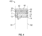
図1A及び図1Bは、いくつかの実施形態によるコイル100の概略上面図及び概略側面図である。コイル100は、情報又はエネルギーを伝達するためのアンテナであってもよく、又はアンテナに使用されてもよい。コイル又はアンテナ100は、幅W、厚さTを有する第1の層10であって、第1の層10の長手方向の第1の端部11と第2の端部12との間で第1の層10の長さに沿って長手方向に延びる第1の層を含む。アンテナ100は、第1の層10の長さに沿って第1の層10に接合された第2の層20を更に含む。第1の層10及び第2の層20は、実質的に同心状の複数のループ110を形成するように巻かれている。第2の層の幅W1及び長さは、第1の層10の互いに反対側にある長手方向縁面13及び14を第1の層10の長さに沿って露出させるように、第1の層の対応する幅W及び長さと実質的に同一の広がりを有する。いくつかの実施形態では、第1の層10は導電性磁気絶縁層であり、第2の層20は導磁性層である。第2の層20は、第2の層20の長さに沿って互いに反対側にある長手方向縁面21及び26を有し、長手方向の第1の端部27及び第2の端部28を有する。層の長手方向縁面は、層の長手方向(例えば、図3Aに示す長手方向123)に延び、層の長手方向端部は、層の長手方向に互いに反対側にある端部に配置される。
1A and 1B are schematic top and side views of a
第1の層の第1の長さ又は幅が第2の層の第1の長さ又は幅と実質的に同一の広がりを有する場合、対応する長さ又は幅は、実質的に互いに重なり合う(例えば、第1の長さ又は幅は、第2の長さ又は幅の少なくとも80%、少なくとも90%、又は少なくとも95%と重なり合い、第1の長さ又は幅は、第1の長さ又は幅の少なくとも80%、少なくとも90%、又は少なくとも95%と重なり合う)。 When the first length or width of the first layer is substantially coextensive with the first length or width of the second layer, the corresponding lengths or widths substantially overlap each other ( For example, the first length or width overlaps at least 80%, at least 90%, or at least 95% of the second length or width, and the first length or width overlaps the first length or width. overlap with at least 80%, at least 90%, or at least 95%).
いくつかの実施形態では、アンテナ又はコイル100は、第1の層10の長さに沿って第1の層10に接合された少なくとも1つの第3の層17を更に含む。各第3の層17は、第1の層10の対応する幅及び長さと実質的に同一の広がりを有する幅及び長さを有する。第1の層10、第2の層20、及び少なくとも1つの第3の層17は、実質的に同心状の複数のループ110を形成するように巻かれている。各第3の層17は、第2の層20の長さに沿って互いに反対側にある長手方向縁面33及び34を有し、長手方向の第1の端部18及び第2の端部19を有する。
In some embodiments, the antenna or
いくつかの実施形態では、コイル100は、第1の層10と少なくとも1つの第3の層17とを接合する第1の接着剤層30を含み、隣接するループ110の間に配置され、隣接するループを接合する第2の接着剤層42を含む。いくつかの実施形態では、第2の接着剤層42は、第1の接着剤層30よりも(例えば、少なくとも1.5又は2倍)厚い。コイル100は、第1の層10を第2の層20に接合する第3の接着剤層40を更に含む。いくつかの実施形態では、第3の接着剤層40は、第1の接着剤層30よりも(例えば、少なくとも1.5又は2倍)厚い。いくつかの実施形態では、少なくとも1つの第3の層117は、少なくとも1つの導電性磁気絶縁層を含む。いくつかの実施形態では、少なくとも1つの第3の層117は、少なくとも1つの導磁性層を含む。
In some embodiments, the
場合によっては、第1の層10と各第3の層17は、例えば、組成、形状、又は機能において類似する。そのような場合又は他の場合には、1つ以上の第3の層17と共に第1の層10を複数の第1の層として説明してもよい。様々な層について代替的な命名法を使用できることが理解されるであろう。例えば、層20を第1の層として説明してもよく、1つ以上の第3の層17と共に層10を複数の第2の層として説明してもよい。
In some cases, the
様々な層の厚さ及び幅を、好適な任意の値となるように選択してもよい。いくつかの実施形態では、より薄い第1の層10及び/又は第3の層17が、コイル又はアンテナをより高い周波数で動作させることが望ましい場合に選択され、より厚い第1の層10及び/又は第3の層17が、コイル又はアンテナをより低い周波数で動作させることが望ましい場合に選択される。より高い周波数では、電流は、導体の表面でスキン層に部分的に閉じ込められる可能性があり、コイルの実効電気抵抗を増加させる傾向がある。複数の第1の層10及び/又は第3の層17を使用することで、電流をより多くの面に分散させ、コイルの実効電気抵抗に対する低減されたスキン深さの影響を低減させることができる。いくつかの実施形態では、第1の層10及び/又は第3の層17はそれぞれ、少なくとも5マイクロメートル、少なくとも10マイクロメートル、少なくとも20マイクロメートル、又は少なくとも40マイクロメートルの厚さを有する。いくつかの実施形態では、第1の層10及び/又は第3の層17はそれぞれ、2000マイクロメートル以下、1000マイクロメートル以下、500マイクロメートル以下、又は250マイクロメートル以下の厚さを有する。例えば、いくつかの実施形態では、1000マイクロメートル≧T≧10マイクロメートルである。層の幅(例えば、W又はW1)は、層の厚さと比べて、小さくてもよく、同等でもよく(例えば、20%以内若しくは10%以内で等しい)、又は大きくてもよい。いくつかの実施形態では、第1の層10の幅の厚さに対する比は、少なくとも0.1、少なくとも1、又は少なくとも5である(すなわち、いくつかの実施形態では、W/T≧0.1、W/T≧1、又はW/T≧5である)。例えば、いくつかの実施形態では、1000≧W/T≧0.1である。第2の層20は厚さT1を有する。いくつかの実施形態では、第2の層20の幅の厚さに対する比は、少なくとも0.1、少なくとも1、少なくとも5、又は少なくとも10である(すなわち、いくつかの実施形態では、W1/T1≧0.1、W1/T1≧1、W1/T1≧5、又はW1/T1≧10である)。例えば、いくつかの実施形態では、1000≧W1/T1≧0.1である。いくつかの実施形態では、第1の層10の厚さTは、第2の層20の厚さT1よりも大きい。他の実施形態では、第1の層10の厚さTは、第2の層20の厚さT1よりも小さい。いくつかの実施形態では、第1の層10の厚さTと第2の層20の厚さT1は、ほぼ等しい。層のうちのいずれかの長さは、層の幅又は厚さよりも実質的に長くてもよい(例えば、長さは、幅及び厚さの一方又は両方の少なくとも5倍又は少なくとも10倍であってもよい)。
The thicknesses and widths of the various layers may be selected to be any suitable values. In some embodiments, a thinner
いくつかの実施形態では、アンテナ又はコイル100を、実質的に同心状の複数のループ110を形成するように巻かれた多層フィルム202を含むものとして説明することができ、多層フィルム202は、第1の層20と、第1の層20に配置及び接合された複数の第2の層(10及び17)とを含む。第1の層10及び少なくとも1つの第3の層17は、第2の層20の同じ側に配置されてもよく、又は、第1の層10及び少なくとも1つの第3の層17のうちの1つ以上は、第2の層20の一方の同じ側に配置されてもよく、第1の層10及び少なくとも1つの第3の層17のうちの残りの層は、第2の層20の反対側に配置されてもよい。
In some embodiments, the antenna or
いくつかの実施形態では、多層フィルム202は、第1の層(例えば、層20)と、第1の層に配置及び接合された、複数の交互する第2の層(例えば、層10及び17)及び第3の層(例えば、層30)とを含む。いくつかの実施形態では、第1の層は導磁性層であり、第2の層は導電性磁気絶縁層であり、第3の層は電気絶縁性かつ磁気絶縁性である。第1の層は、導磁性層について本明細書の他の箇所で説明する範囲のうちのいずれかの比透磁率を有してもよい。第1の層は、導電性であってもよく、又は電気絶縁性であってもよい。第2及び/又は第3の層は、磁気絶縁層について本明細書の他の箇所で説明する範囲のうちのいずれかの比透磁率を有してもよい。各第3の層は、接着剤(例えば、熱硬化性接着剤及び/又はエポキシ)であり得る。いくつかの実施形態では、第1、第2、及び第3の層の幅及び長さは、第2の層の長手方向縁面(例えば、縁面13及び14)が第3の層又は第1の層のいずれによっても覆われないように、実質的に互いに同一の広がりを有する。
In some embodiments,
アンテナ又はコイル100は、互いに反対側にある主面76及び77を含む。主面76及び77の一方又は両方は、本明細書の他の箇所で更に説明するように、規則的パターン(例えば、実質的に平行な溝の規則的パターン)を含んでもよい。例えば、いくつかの実施形態では、規則的パターンを、以下の方法のうちの任意の1つ以上で説明してもよい。規則的パターンは、実質的にコイル全体にわたって、同じ第1の方向に実質的に沿って延びてもよい。規則的パターンは、ループの長手方向と角度θをなす第1の方向に沿って延びてもよく、θは、ループの長手方向に沿って変化する。多層フィルムの分離部分の隣接する少なくとも複数のループの縁面の規則的パターンは、実質的に互いに位置合わせされていてもよい。規則的パターンは、多層フィルムの分離部分の隣接する少なくとも複数のループにわたって延びる、実質的に平行な溝のパターンを含んでもよい。規則的パターンは、コイルの第1の領域における第1の平均ピッチと、コイルの異なる第2の領域における異なる第2の平均ピッチとを有してもよい。規則的パターンのフーリエ変換が、コイルの第1の領域における第1の空間周波数でのピークと、コイルの異なる第2の領域における異なる第2の空間周波数でのピークとを有してもよい。コイルは、コイルの少なくとも1つの第1の領域において、第1の方向に沿った光学的かつトポグラフィ的である規則的パターンと、直交する第2の方向に沿った光学的であるがトポグラフィ的でない規則的パターンとを含んでもよい。
Antenna or
図1Cは、ループ110の長手方向と垂直な断面における多層フィルム202の概略断面図である。多層フィルム202は、実質的に矩形の断面を有する。例えば、断面は名目上矩形であってもよく、又は、フィルムの厚さと比べて(例えば、少なくとも5倍、少なくとも10倍、若しくは少なくとも20倍)大きな曲率半径を有する丸みを帯びたコーナーを除いて、及び/又は20度以下、10度以下、若しくは5度以下で平行からずれた互いに反対の側を有することを除いて、矩形であってもよい。矩形は、様々な層の幅及び厚さに応じて、x方向をy方向よりも長く、又は短くすることができる。正方形は矩形の特殊な場合と見なすことができるため、実質的に矩形の断面はまた、実質的に正方形の断面も含む。いくつかの実施形態では、実質的に同心状の複数のループ110のうちの各ループについて、多層フィルム202は、ループの長手方向と垂直な平面において実質的に矩形の断面を有する。いくつかの実施形態では、同心状の複数のループ110のうちの各ループは、ループの長手方向と垂直な平面において実質的に矩形の断面を有する。
FIG. 1C is a schematic cross-sectional view of
図1Dは、コイル100及びロッド37を含むアセンブリ101の概略上面図である。本明細書の他の箇所で更に説明するように、アセンブリ101は、ロッドに多層フィルムを巻き付け、得られたアセンブリを、切断によって分離されたアセンブリの部分が所望の幅をもたらすように切断する(例えば、ワイヤソーでスライスする)ことによって製造することができる。ロッド37は、アセンブリ101を形成する際に使用された初期ロッドのスライスされたセグメントであってもよい。
FIG. ID is a schematic top view of assembly 101 including
第1の層10及び任意選択的な少なくとも1つの第3の層17はそれぞれ、導電性磁気絶縁層、金属層、非鉄金属層、又は実質的に非磁性の金属層のうちの1つ以上であってもよく、本明細書の他の箇所で説明する対応する範囲のうちのいずれかの伝導率及び/又は比透磁率を有してもよく、本明細書の他の箇所で説明する対応する材料(例えば、銅又は銅合金)で作られてもよい。第2の層20は、導磁性層又は軟磁性層の1つ以上であってもよく、本明細書の他の箇所で説明する対応する範囲のうちのいずれかの比透磁率及び/又は保磁力を有してもよく、本明細書の他の箇所で説明する対応する材料(例えば、バインダ中の鉄-ケイ素-ホウ素-ニオブ-銅合金の粒子)で作られてもよい。いくつかの実施形態では、各ループは、1.1未満の比透磁率を有する少なくとも1つの金属層(例えば、層10)と、少なくとも10の比透磁率を有する少なくとも1つの層(例えば、層20)とを含む。いくつかの実施形態では、各ループ110は、少なくとも1つの実質的に非磁性の金属層(例えば、層10)と、少なくとも1つの軟磁性層(例えば、層20)とを含む。いくつかの実施形態では、各ループ110は、少なくとも1つの導電性磁気絶縁層(例えば、層10)と、少なくとも1つの導磁性層(例えば、層20)とを含む。いくつかの実施形態では、各ループ110は、100μΩcm未満の電気抵抗率及び1.4未満の比透磁率を有する少なくとも1つの第1の層(例えば、層10及び/又は17)と、2超の比透磁率及び1000A/m未満の保磁力を有する少なくとも1つの第2の層(例えば、層20)とを含む。いくつかの実施形態では、各ループは、100μΩcm未満の電気抵抗率及び1.1未満の比透磁率を有する少なくとも1つの第1の層(例えば、層10及び/又は17)と、10超の比透磁率及び100A/m未満の保磁力を有する少なくとも1つの第2の層(例えば、層20)とを含む。
The
いくつかの実施形態では、情報又はエネルギーを伝達するためのコイル又はアンテナ100は、導電性磁気絶縁性の第1の層10であって、互いに反対側にある主面15及び16と、互いに反対側にある主面15及び16を接続する互いに反対側にある縁面13及び14とを含む第1の層10と、第1の層10に配置及び接合され、第1の層の縁面13及び14を覆わないように第1の層10の長さ及び幅と実質的に同一の広がりを有する、導磁性の第2の層20であって、第1の層10及び第2の層20が、実質的に同心状の複数のループ110を形成するように巻かれている、第2の層とを含む。
In some embodiments, a coil or
いくつかの実施形態では、コイル100は、実質的に平面状である。例えば、コイル100は、図示するx-y-z座標系を基準とする図1A~図1Dのx-y平面と平行な平面に主に配置されてもよく、コイルの平面と垂直な平面におけるコイルの断面の任意の曲率半径が、コイルの直径又は最大横寸法と比べて(例えば、少なくとも5倍、少なくとも10倍、又は少なくとも20倍)大きい。
In some embodiments,
いくつかの実施形態では、情報又はエネルギーを伝達するための実質的に平面状のコイル100が、導電性磁気絶縁性の第1の層10と、第1の層10に配置及び接合され、第1の層10の縁面13及び14を覆わないように第1の層の長さ及び幅と実質的に同一の広がりを有する、導磁性の第2の層20とを含む。
In some embodiments, a substantially
アンテナ又はコイル100のいくつかの実施形態では、第1の層10及び第2の層20の対応する縁面(13、21及び14、22)は、実質的に同一平面(例えば、図4及び図5Aに示す平面S1及びS2を参照)上にある。本明細書の他の箇所で説明する方法は、いくつかの実施形態では、第2の層20が、第1の層10の縁面13及び14を覆わないように第1の層の長さ及び幅と実質的に同一の広がりを有することを確実にすることができ、いくつかの実施形態では、実質的に同一平面上にある第1の層10及び第2の層20の対応する縁面を形成することができる。
In some embodiments of the antenna or
コイル100は、第2の層20を第1の層10の外側にしてループに巻かれている。コイルは、代わりに、第1の層10を第2の層20の外側にしてループに巻かれてもよい。図2は、第1の層10を第2の層20の外側にして巻かれたアンテナ又はコイル200の概略上面図である。図示した実施形態では、コイル200は、第1の層10が第2の層20と少なくとも1つの第3の層17との間に配置された、少なくとも1つの第3の層17を含む。
The
図3A及び図3Bは、第1の層10の互いに反対側にある長手方向縁面の少なくとも一方が規則的パターン120を含む、アンテナ又はコイル300の概略上面図である。図3Cは、いくつかの実施形態によるアンテナ又はコイル300の概略下面図である。規則的パターン120は、例えば、溝の規則的パターンであり得る。いくつかの実施形態では、長手方向縁面13は、第1の規則的パターン(例えば、上平面図に規則的パターン120として現れる)を含み、長手方向縁面14は、第2の規則的パターン(例えば、下平面図に規則的パターン120bとして現れる)を含む。他の実施形態では、規則的パターンは、上平面図及び下平面図の一方又は他方にのみ存在する。コイル100及び/又は200は、例えばコイル300について説明した規則的パターンを含んでもよい。
3A and 3B are schematic top views of an antenna or coil 300 in which at least one of the opposing longitudinal edge surfaces of the
いくつかの実施形態では、実質的に同心状の複数のループ110のうちの各ループ110aは、隣接するループ110bと実質的に垂直な(例えば、垂直に対して20度以内、10度以内、又は5度以内で)縁面111を有し、規則的パターン120を含む。いくつかの実施形態では、規則的パターン120は、ループ110の長手方向123と角度θをなす第1の方向122に沿って延び、θは、ループ110の長手方向123に沿って変化する。いくつかの実施形態では、規則的パターン120は、((例えば、x-y平面と平行な)縁面111を含むコイルの主面の平面の20度以内、10度以内、5度以内、又は3度以内で)縁面111にわたって実質的に横方向に延びる。いくつかの実施形態では、規則的パターン120は、縁面111にわたって実質的に横方向に、同じ第1の方向122に実質的に沿って延びる。いくつかの実施形態では、隣接する少なくとも複数のループ110の縁面111の規則的パターン120は、実質的に互いに位置合わせされている。いくつかの実施形態では、各ループは、縁面111(第1の縁面)とは反対側の第2の縁面111b(例えば、図3Cを参照)を含み、第2の縁面111bは、第2の縁面111bにわたって実質的に横方向に延びてもよく、第1の方向122に沿って延びてもよい、第2の規則的パターン120bを含む。
In some embodiments, each loop 110a of the plurality of substantially
第2の規則的パターン120bは、規則的パターン120について本明細書の他の箇所で更に説明する属性のうちのいずれを有してもよい。例えば、第2の規則的パターン120bは、実質的に同心状の複数のループのうちの隣接する少なくとも複数のループにわたって延びる、実質的に平行な溝の規則的パターンであってもよい。 Second regular pattern 120b may have any of the attributes further described for regular pattern 120 elsewhere herein. For example, the second regular pattern 120b may be a regular pattern of substantially parallel grooves extending across at least a plurality of adjacent loops of the plurality of substantially concentric loops.
いくつかの実施形態では、実質的に同心状のループは、例えば、多層フィルムのループを指す。各ループ110は、隣接する層10及び17のループを含んでもよく、縁面111は、組み合わされた隣接する層10及び17の縁面であってもよい。いくつかの実施形態では、実質的に同心状のループは、例えば、多層フィルム内の個々の層のループを指す。例えば、第1の層10は、実質的に同心状のループに巻かれている。そのような場合、縁面111は、例えば、第1の層10の縁面(例えば、縁面13)であってもよい。
In some embodiments, substantially concentric loops refer to, for example, loops of a multilayer film. Each
いくつかの実施形態では、各ループ110は、軟磁性層及び/又は磁気絶縁層である少なくとも1つの層(例えば、層20)と、金属層などの導電層である少なくとも1つの層(例えば、層10及び/又は17)とを含む。いくつかの実施形態では、任意選択的な少なくとも1つの第3の層17は省略される。いくつかの実施形態では、各ループは、複数の導電性又は金属性の層(例えば、層10及び17)を含む。いくつかの実施形態では、各ループは、2つ以上の軟磁性及び/又は磁気絶縁性の層を含む。
In some embodiments, each
いくつかの実施形態では、コイル300は、実質的に同心状の複数のループ110を含み、各ループは、少なくとも1つの軟磁性層20と実質的に同心状である実質的に同心状の複数の金属層(10及び17)を含み、平面図(例えば、図3A又は図3Bの上平面図及び/又は図3Cの下平面図)において、コイル300が、実質的に同心状の複数のループ110のうちの隣接する少なくとも複数のループにわたって延びる、実質的に平行な溝121の規則的パターン120を含むようになっている。いくつかの実施形態では、上平面図において、コイルは規則的パターン120(第1の規則的パターン)を含み、下平面図において、コイルは規則的パターン120b(第2の規則的パターン)を含む。いくつかの実施形態では、第1及び第2の規則的パターンはそれぞれ、実質的に平行な溝のパターンを含む。いくつかの実施形態では、第1及び第2の規則的パターンは、実質的に同じ第1の方向122に延びる。
In some embodiments, the coil 300 includes a plurality of substantially
いくつかの実施形態では、各ループの少なくとも1つの軟磁性層は、ループの実質的に同心状の複数の金属層と、隣接するループの実質的に同心状の複数の金属層との間に配置される。いくつかの実施形態では、第1の接着剤層30が、実質的に同心状の複数の金属層のうちの隣接する金属層の間に配置され、隣接する金属層を接合し、第2の接着剤層42が、隣接するループの間に配置され、隣接するループを接合する。いくつかの実施形態では、第2の接着剤層42は、第1の接着剤層30よりも厚い。
In some embodiments, the at least one soft magnetic layer of each loop is between the substantially concentric plurality of metal layers of the loop and the substantially concentric plurality of metal layers of an adjacent loop. Placed. In some embodiments, a first adhesive layer 30 is disposed between adjacent metal layers of the plurality of substantially concentric metal layers to bond the adjacent metal layers and An
いくつかの実施形態では、各ループ内の実質的に同心状の複数の金属層は、互いに電気的に接続される。例えば、コイルが、例えばはんだ付けにより、電気ケーブルに接続されるときに、各ループ内の金属層は、ループの一方若しくは両方の端部で一緒に溶接されてもよく、又はループの一方若しくは両方の端部で互いに電気的に接続されてもよい。溶接部15が、図3Bに概略的に示されている。層10及び17の反対側の端部も、層間に電気的接続をもたらすために、任意選択的に溶接又ははんだ付けされてもよい。
In some embodiments, the substantially concentric metal layers within each loop are electrically connected to each other. For example, when the coil is connected to an electrical cable, for example by soldering, the metal layers within each loop may be welded together at one or both ends of the loop, or at one or both ends of the loop. may be electrically connected to each other at their ends. A
いくつかの実施形態では、アンテナ又はコイル300は、実質的に同心状の複数のループ110を含み、各ループは金属層(例えば、層10)を含む。各ループは、少なくとも1つの軟磁性層を更に含んでもよく、かつ/又は、本明細書の他の箇所で更に説明するように、複数の交互する金属層及び第1の接着剤層を含んでもよい。いくつかの実施形態では、平面図(例えば、図3Aの上平面図)において、コイル300は、実質的にコイル300の全体にわたって(例えば、コイルの面積の少なくとも80%、少なくとも90%、又は少なくとも95%にわたって)、同じ第1の方向122に実質的に沿って延びる(例えば、第1の方向122の20度以内、10度以内、又は5度以内で第1の方向122に沿って延びる)、規則的パターン120を含む。様々な領域における平均ピッチの観点、及び/又は様々な領域における規則的パターンのフーリエ変換の観点から、規則的パターン120を説明することができる。いくつかの実施形態では、規則的パターンは、コイルの第1の領域125における第1の平均ピッチP1と、コイルの異なる第2の領域130における異なる第2の平均ピッチP2とを有する。いくつかの実施形態では、第1の平均ピッチと第2の平均ピッチとの間の差が、約10マイクロメートル超、約15マイクロメートル超、約20マイクロメートル超、約30マイクロメートル超、約40マイクロメートル超、又は約50マイクロメートル超である。例えば、第1の平均ピッチP1は、約60マイクロメートル~約100マイクロメートルの範囲内であってもよく、第2の平均ピッチP2は、約120マイクロメートル~約200マイクロメートルの範囲内であってもよい。いくつかの実施形態では、第1及び第2の平均ピッチの一方又は両方は、5マイクロメートル、10マイクロメートル、20マイクロメートル、又は40マイクロメートル~2000マイクロメートル、1000マイクロメートル、500マイクロメートル、又は250マイクロメートルの範囲内である。
In some embodiments, the antenna or coil 300 includes a plurality of substantially
いくつかの実施形態では、規則的パターンのフーリエ変換が、コイルの第1の領域125における第1の空間周波数(例えば、図14に示すF1を参照)でのピークと、コイルの異なる第2の領域130における異なる第2の空間周波数(例えば、図21に示すF2を参照)でのピークとを有する。フーリエ変換のピークは、規則的パターンの平均ピッチに対応してもよい(例えば、F1は約1/P1であってもよく、F2は約1/P2であってもよい)。いくつかの実施形態では、第1及び第2の空間周波数の一方又は両方は、1/(2000マイクロメートル)、1/(1000マイクロメートル)、1/(500マイクロメートル)、又は1/(250マイクロメートル)~1/(5マイクロメートル)、1/(10マイクロメートル)、1/(20マイクロメートル)、又は1/(40マイクロメートル)の範囲内である。いくつかの実施形態では、第1の空間周波数と第2の空間周波数との間の差が、約0.001毎マイクロメートル超、約0.002毎マイクロメートル超、約0.004毎マイクロメートル超、約0.01毎マイクロメートル超、約0.02毎マイクロメートル超、約0.05毎マイクロメートル超、又は約0.1毎マイクロメートル超である。 In some embodiments, the Fourier transform of the regular pattern has a peak at a first spatial frequency in the first region 125 of the coil (e.g., see F1 shown in FIG. and a peak at a different second spatial frequency in region 130 (see, for example, F2 shown in FIG. 21). The peaks of the Fourier transform may correspond to the average pitch of the regular pattern (eg, F1 may be about 1/P1 and F2 may be about 1/P2). In some embodiments, one or both of the first and second spatial frequencies are 1/(2000 micrometers), 1/(1000 micrometers), 1/(500 micrometers), or 1/(250 micrometers). micrometers) to 1/(5 micrometers), 1/(10 micrometers), 1/(20 micrometers), or 1/(40 micrometers). In some embodiments, the difference between the first spatial frequency and the second spatial frequency is greater than about 0.001 per micrometer, greater than about 0.002 per micrometer, or greater than about 0.004 per micrometer. greater than about 0.01 per micrometer, greater than about 0.02 per micrometer, greater than about 0.05 per micrometer, or greater than about 0.1 per micrometer.
第3の領域131及び第4の領域139もまた、図3Bに示されている。ピッチ及びフーリエ変換は、本明細書の他の箇所で更に説明するように、これらの領域のそれぞれで評価することができる。 A third region 131 and a fourth region 139 are also shown in FIG. 3B. Pitch and Fourier transforms can be evaluated in each of these regions, as further described elsewhere herein.
いくつかの実施形態では、本説明のコイル又はアンテナ(例えば、100、200、又は300)を、実質的に同心状の複数のループ(例えば、ループ110)を形成するように巻かれた多層フィルムを含むものとして説明することができる。 In some embodiments, a coil or antenna (e.g., 100, 200, or 300) of the present description is wrapped in a multilayer film wound to form a plurality of substantially concentric loops (e.g., loop 110). It can be described as including.
図4は、第1の層10及び第2の層20を含む多層フィルム402の実施形態の概略端面図である。第1の層10は導電性磁気絶縁層であってもよく、第2の層20は導磁性層及び/又は軟磁性層であってもよい。いくつかの実施形態では、第1の層10及び第2の層20は、接着剤40によって互いに接合される。いくつかの実施形態では、多層フィルムが、一方のフィルムの接着剤42が他方のフィルムの第1の層10に接続された、2つの多層フィルム402を含む。そのような実施形態では、多層フィルムは、2つの第1の層10及び2つの第2の層20を含む。いくつかの実施形態では、アンテナ又はコイルが、複数のループに巻かれた多層フィルム402を含む。いくつかの実施形態では、接着剤42は、隣接するループを互いに接合する。
FIG. 4 is a schematic end view of an embodiment of a
いくつかの実施形態では、多層フィルム402は、導電性磁気絶縁性の第1の層10と、第1の層10に配置及び接合された導磁性の第2の層20とを含み、第1の層10及び第2の層20の対応する縁面は、実質的に同一平面上にある(例えば、共通平面からのずれが多層フィルムの厚さの0.3倍未満、0.2倍未満、0.1倍未満、又は0.05倍未満以内の同一平面上にある)。図示した実施形態では、第1の層10の縁面13及び第2の層20の縁面21は、平面S1の対応する縁面であり、第1の層10の縁面14及び第2の層20の縁面24は、平面S2の対応する縁面である。
In some embodiments, the
いくつかの実施形態では、多層フィルムが、追加の第1の層10及び/又は追加の第2の層20を含む。図5Aは、第1の層20と、複数の交互する第2の層10及び第3の層30とを含む多層フィルム502の概略端面図である。図5Bは、多層フィルム502の概略側面図である。いくつかの実施形態では、多層フィルム502は、導磁性の第1の層20と、第1の層20に配置及び接合された複数の交互する第2の層10及び第3の層30とを含み、第2の層10は導電性かつ磁気絶縁性であり、第3の層30は電気絶縁性かつ磁気絶縁性である。いくつかの実施形態では、第1の層20、第2の層10、及び第3の層30の幅(W1、W、W2)及び長さ(L1、L、L2)が、第2の層10の長手方向縁面(13、14)が第3の層30又は第1の層20のいずれによっても覆われないように、実質的に互いに同一の広がりを有する。いくつかの実施形態では、第1の層20の幅の厚さに対する比が、少なくとも0.1、少なくとも1、又は少なくとも5である。
In some embodiments, the multilayer film includes an additional
いくつかの実施形態では、コイルが、実質的に同心状の複数のループ(例えば、ループ110)を形成するように巻かれた多層フィルム(例えば、202、402、又は502)を含む。いくつかの実施形態では、多層フィルムは、複数の交互する導電層10及び第1の接着剤層30を含み、多層フィルムの最も外側の主面44を含む第2の接着剤層42を含む。第2の接着剤層42は、任意選択的に、図4~図5Bに示すものとは反対側の最も外側の主面に配置することができる。いくつかの実施形態では、本明細書の他の箇所で更に説明するように、コイルを製造する方法が、ロッドに多層フィルムを巻き付けて、ロッドと、ロッドと実質的に同心状の多層フィルムの複数のループとを含むアセンブリであって、各ループが第2の接着剤層42によって隣接するループに接合される、アセンブリを形成することを含む。
In some embodiments, the coil includes a multilayer film (eg, 202, 402, or 502) wound to form a plurality of substantially concentric loops (eg, loop 110). In some embodiments, the multilayer film includes a plurality of alternating
フィルムが、第3の寸法よりもはるかに大きな2つの寸法を有してもよい。フィルムストリップを、ストリップが他の2つの寸法よりもはるかに大きな1つの寸法を有するように、フィルムから切り出すことができる。本説明のコイル又はアンテナに使用される多層フィルムが、フィルムストリップ又はフィルムストリップの一部分であってもよい。 The film may have two dimensions that are much larger than the third dimension. Film strips can be cut from the film such that the strip has one dimension that is much larger than the other two dimensions. The multilayer film used in the coil or antenna described herein may be a filmstrip or a portion of a filmstrip.
図6は、コイル600と、ロッド又はロッドセクション637とを含むアセンブリ601の上面図である。コイル600は、実質的に同心状の複数のループ110を含む。図7Aは、150倍率のZ20レンズを取り付けたKeyence VHX-5000デジタル顕微鏡を使用して得られた、コイル600に対応するコイルの一部分のレーザー強度画像である。図7Bは、コイル600に対応し得るコイルの一部分の概略上平面図である。図7Bのコイルは、曲率が図7Bの概略図に示されないような、図示した部分のサイズと比べて大き曲率を有するとみなされる。
FIG. 6 is a top view of an assembly 601 that includes a coil 600 and a rod or rod section 637. Coil 600 includes a plurality of substantially
いくつかの実施形態では、コイルは、実質的に同心状の複数のループを含み、各ループは多層フィルムのループである(例えば、図7Bに示すループ110は、複数の層10及び30を含む)。いくつかの実施形態では、コイルは、実質的に同心状の複数のループを含み、各ループは、第1の層のループである(例えば、図7A又は図7Bに示すループ10a及び10bは、単一層10の各ループである)。いくつかの実施形態では、コイル600が、実質的に同心状の複数のループ110を含み、各ループは、実質的に同心状の複数の交互する金属層10及び第1の接着剤層30を含む(例えば、図7A又は図7Bに示す各ループ110a及び110bはそれぞれ、交互する層10及び30を含む)。いくつかの実施形態では、各金属層は、非鉄金属を含み、かつ/又は磁気絶縁性であり、かつ/又は実質的に非磁性である。
In some embodiments, the coil includes a plurality of substantially concentric loops, each loop being a loop of multilayer film (e.g.,
第2の接着剤層41が、隣接するループ110の間に配置され、隣接するループを接合する。いくつかの実施形態では、第2の接着剤層41は、第1の接着剤層30よりも厚い。いくつかの実施形態では、第2の接着剤層41は、少なくとも2倍又は少なくとも4倍、第1の接着剤層よりも厚い。いくつかの実施形態では、第2の接着剤層41は、バインダ中に分散した導磁性フィラーを含む。
A second adhesive layer 41 is placed between
いくつかの実施形態では、第2の接着剤層41は、複合部分20の互いに反対側にある主面に、互いに反対側にある第1の接着剤部分40及び第2の接着剤部分42を含む。複合部分20は、導磁性フィラーの粒子であり得る、バインダ(例えば、エポキシ)中に分散した粒子43を含む。いくつかの実施形態では、接着剤部分40及び42並びに複合部分20はそれぞれ、共通の種類の接着剤材料を含む。例えば、いくつかの実施形態では、接着剤部分40及び42並びに複合部分20はそれぞれ、エポキシを含む。いくつかの実施形態では、複合部分20は、例えば、複合部分20の比透磁率を高めるために、複合部分20の全体に分散した導磁性フィラーの粒子を含む。粒子43は、例えば、鉄-ケイ素-ホウ素-ニオブ-銅合金を含み得る、好適な任意の形状(例えば、薄片、板、球、楕円、不規則形状の粒子のうちの少なくとも1つ)を有し得る、金属粒子であってもよい。
In some embodiments, the second adhesive layer 41 includes opposing first and second
いくつかの実施形態では、アンテナ又はコイルが、実質的に同心状の複数のループ110を含み、各ループは、実質的に同心状の複数の交互する金属層10及び第1の接着剤層30を含み、第2の接着剤層41は、隣接するループの間に配置され、隣接するループを接合する。いくつかの実施形態では、第2の接着剤層は、第1の接着剤層よりも(例えば、少なくとも2倍又は4倍)厚い。いくつかの実施形態では、第1の接着剤部分40及び第2の接着剤部分42はそれぞれ、各第1の接着剤層30よりも厚い。いくつかの実施形態では、複合部分20は、第1の接着剤部分40及び第2の接着剤部分42のそれぞれよりも厚い。いくつかの実施形態では、第1の接着剤部分40及び第2の接着剤部分42は、実質的に同じ(例えば、20%以内、10%以内、又は5%以内までの)厚さを有する。
In some embodiments, the antenna or coil includes a plurality of substantially
いくつかの実施形態では、アンテナ又はコイルは、実質的に同心状の複数のループを形成するように巻かれた多層フィルムを含み、多層フィルムは、導磁性の第1の層20と、複数の交互する第2の層10及び第3の層30とを含む。第1の層20は、複数の交互する第2の層10及び第3の層30に接着剤層40によって接合される。隣接するループが、接着剤層42によって一緒に接合される。いくつかの実施形態では、接着剤層42は、各層30よりも厚い。いくつかの実施形態では、接着剤層42は、各層30よりも少なくとも1.5倍又は少なくとも2倍、厚い。
In some embodiments, the antenna or coil includes a multilayer film wound to form a plurality of substantially concentric loops, the multilayer film comprising a magnetically conductive
図8A及び図8Bはそれぞれ、Keyence VK-X200共焦点顕微鏡を20倍率対物レンズと共に使用して、(例えば、図8に示すx-y-z座標系を基準とするx-y平面の)上平面図において得られた、アンテナ800の第1の領域(例えば、図3Bに示す第1の領域125に対応する)におけるコイル又はアンテナ800のレーザー強度画像及びトポグラフィマップである。いくつかの実施形態では、アンテナ800は、情報又はエネルギーを伝達するためのものであり、実質的に同心状の複数のループ110を含み、各ループは金属層10を含む。いくつかの実施形態では、各ループ110は、複数の金属層10(例えば、図示した実施形態では、4つの金属層10)を含む。コイル又はアンテナ800は、10マイクロメートル厚のエポキシ接着剤層30によって一緒に接合された4つの銅層と、約60マイクロメートルの厚さを有し、20マイクロメートル厚のエポキシ接着剤層(例えば、図7Bに示す層40に対応する)によって銅層に接合され、多層フィルムの隣接するループを一緒に接合するための20マイクロメートル厚のエポキシ接着剤層(例えば、図7Bに示す層42に対応する)を有する、複合層(例えば、図7Bに示す層20に対応する)を含む接着剤層41とを含む多層フィルムから製造された。銅層の厚さは、約105マイクロメートルであった。複合層は、エポキシ中に分散した磁性金属(センダスト)の薄片を含んでいた。コイル又はアンテナ800は、本明細書の他の箇所で更に説明するように、ロッドに多層フィルムを巻き付けて、実質的に同心状の複数のループを形成し、得られたアセンブリからコイル又はアンテナ800をダイヤモンドワイヤソーを使用してスライスすることにより製造された。
FIGS. 8A and 8B are images taken using a Keyence VK-X200 confocal microscope with a 20x objective, respectively (e.g., in the xy plane relative to the xyz coordinate system shown in FIG. 8). 3B is a laser intensity image and topography map of the coil or antenna 800 in a first region of the antenna 800 (e.g., corresponding to the first region 125 shown in FIG. 3B) taken in plan view. In some embodiments, the antenna 800 is for transmitting information or energy and includes a plurality of substantially
図9は、Keyence VK-X200共焦点顕微鏡を使用して得られた、第1の領域の一部分のトポグラフィマップである。図10は、x方向に沿ったトポグラフィ(基準平面に対する表面高さ)のプロットであり、図11は、第1の領域におけるy方向に沿ったトポグラフィ(高さ)のプロットである。Keyence VK-X200共焦点顕微鏡を使用して得られた形態(topological)マップから、図10及び図11のプロットを抽出した。x方向及びy方向の両方に光学パターンが存在することを図8A~図9に見ることができる。図10では、複数の金属層にわたってy方向に沿ってトポグラフィ的なパターンが実質的に存在しないことが分かる。図11では、複数の金属層にわたってy方向に沿って実質的なトポグラフィ的なパターンが存在することが分かる。第1の領域における形態パターンは、y方向で約89マイクロメートルの平均ピッチP1(対応するフーリエ変換ピーク周波数の逆数として平均ピッチを近似することによって決定された)を有していた。いくつかの実施形態では、(例えば、x-y平面内の)平面図及びアンテナ又はコイルの少なくとも1つの第1の領域125において、アンテナ又はコイルは、第1の方向(y方向)に沿った光学的かつトポグラフィ的である規則的パターン120と、直交する第2の方向(x方向)に沿った光学的であるがトポグラフィ的でない規則的パターンとを含む。いくつかの実施形態では、上平面図及びアンテナ又はコイルの少なくとも1つの第1の領域125において、アンテナ又はコイルは、第1の方向(y方向)に沿った光学的かつトポグラフィ的な第1の規則的パターン120と、直交する第2の方向(x方向)に沿った光学的であるがトポグラフィ的でない第1の規則的パターンとを含み、下平面図及びアンテナ又はコイルの少なくとも1つの第1の領域125において、アンテナ又はコイルは、第1の方向に沿った光学的かつトポグラフィ的である第2の規則的パターン120b(図3Cに概略的に示す)と、直交する第2の方向に沿った光学的であるがトポグラフィ的でない第2の規則的パターンとを含む。 FIG. 9 is a topography map of a portion of the first region obtained using a Keyence VK-X200 confocal microscope. FIG. 10 is a plot of the topography (surface height relative to the reference plane) along the x direction, and FIG. 11 is a plot of the topography (height) along the y direction in the first region. The plots in Figures 10 and 11 were extracted from topological maps obtained using a Keyence VK-X200 confocal microscope. The presence of optical patterns in both the x and y directions can be seen in FIGS. 8A-9. In FIG. 10, it can be seen that there is virtually no topographical pattern along the y-direction across the metal layers. In FIG. 11, it can be seen that there is a substantial topographical pattern along the y-direction across multiple metal layers. The morphology pattern in the first region had an average pitch P1 (determined by approximating the average pitch as the reciprocal of the corresponding Fourier transform peak frequency) of approximately 89 micrometers in the y direction. In some embodiments, in a plan view (e.g., in the xy plane) and at least one first region 125 of the antenna or coil, the antenna or coil is aligned It includes a regular pattern 120 that is both optical and topographical and a regular pattern that is optical but not topographical along a second orthogonal direction (the x direction). In some embodiments, in the top plan view and at least one first region 125 of the antenna or coil, the antenna or coil has an optical and topographic first region along a first direction (y-direction). a regular pattern 120 and a first optical but non-topographical regular pattern along an orthogonal second direction (x-direction); In the region 125, the antenna or coil forms a second regular pattern 120b (schematically shown in FIG. 3C) that is both optical and topographical along a first direction and along a second orthogonal direction. a second regular pattern that is optical but non-topographical;
いくつかの実施形態では、光学的かつトポグラフィ的である規則的パターン120及び/又は120bは、第2の方向に沿って延び、第1の方向に沿って間隔を空けた、実質的に平行な溝の規則的パターンを含む。いくつかの実施形態では、実質的に平行な溝の規則的パターンは、実質的にアンテナ又はコイルの全体にわたって延び、実質的に平行な溝の規則的パターンは、アンテナ又はコイルの第1の領域における第1の平均ピッチを有し、アンテナ又はコイルの異なる第2の領域における異なる第2の平均ピッチを有する。いくつかの実施形態では、実質的に平行な溝の規則的パターンは、実質的にアンテナの全体にわたって延び、実質的に平行な溝の規則的パターンのフーリエ変換が、アンテナの第1の領域における第1の空間周波数でのピークと、アンテナの異なる第2の領域における異なる第2の空間周波数でのピークとを有する。 In some embodiments, the regular optical and topographical patterns 120 and/or 120b extend along the second direction and include substantially parallel, spaced apart patterns along the first direction. Contains a regular pattern of grooves. In some embodiments, the regular pattern of substantially parallel grooves extends substantially throughout the antenna or coil, and the regular pattern of substantially parallel grooves extends across a first region of the antenna or coil. and a different second average pitch in a different second region of the antenna or coil. In some embodiments, the regular pattern of substantially parallel grooves extends substantially throughout the antenna, and the Fourier transform of the regular pattern of substantially parallel grooves in the first region of the antenna is It has a peak at a first spatial frequency and a peak at a different second spatial frequency in a different second region of the antenna.
図12は、第1の領域における表面トポグラフィの2次元フーリエ変換の大きさのプロットである。図13は、x方向に沿ったフーリエ変換の大きさのプロットであり、図14は、第1の領域におけるy方向に沿ったフーリエ変換の大きさのプロットである。y方向に沿ったフーリエ変換は、空間周波数F1でのピークK1を有する。ピークK1は、図11に示す周期的パターンを示す。ピークK1は、隣接する任意のピークから実質的に間隔を空けている。図13に示すx方向に沿ったフーリエ変換は、隣接する任意のピークから実質的に間隔を空けた非ゼロ空間周波数でのピークを有していない。このことは、x方向に沿った形態パターンの欠如を示す。 FIG. 12 is a plot of the two-dimensional Fourier transform magnitude of the surface topography in the first region. FIG. 13 is a plot of the Fourier transform magnitude along the x direction, and FIG. 14 is a plot of the Fourier transform magnitude along the y direction in the first region. The Fourier transform along the y direction has a peak K1 at spatial frequency F1. Peak K1 indicates the periodic pattern shown in FIG. Peak K1 is substantially spaced apart from any adjacent peaks. The Fourier transform along the x direction shown in FIG. 13 has no peaks at non-zero spatial frequencies that are substantially spaced apart from any adjacent peaks. This indicates a lack of morphological pattern along the x direction.
図15A及び図15Bはそれぞれ、Keyence VK-X200共焦点顕微鏡を使用して上平面図において得られた、コイル又はアンテナ800の第2の領域(例えば、図3Bに示す第2の領域130に対応する)におけるコイル又はアンテナ800のレーザー強度画像及びトポグラフィマップである。図16は、第2の領域の一部分のトポグラフィマップである。図17は、x方向に沿った高さのプロットであり、図18は、第2の領域におけるy方向に沿った高さのプロットである。第2の領域における形態パターンは、y方向で約152マイクロメートルの平均ピッチP2を有していた。 15A and 15B each correspond to a second region of the coil or antenna 800 (e.g., second region 130 shown in FIG. 3B) obtained in top plan view using a Keyence VK-X200 confocal microscope. FIG. 8 is a laser intensity image and topography map of a coil or antenna 800 in FIG. FIG. 16 is a topography map of a portion of the second region. FIG. 17 is a plot of height along the x direction, and FIG. 18 is a plot of height along the y direction in the second region. The feature pattern in the second region had an average pitch P2 of approximately 152 micrometers in the y direction.
図19は、第2の領域における表面トポグラフィのフーリエ変換の大きさのプロットである。図20は、x方向に沿ったフーリエ変換の大きさのプロットであり、図21は、第2の領域におけるy方向に沿ったフーリエ変換の大きさのプロットである。y方向に沿ったフーリエ変換は、空間周波数F2でのピークK2を有する。ピークK2は、図18に示す周期的パターンを示す。ピークK2は、同様の大きさを有する隣接する任意のピークから実質的に間隔を空けている。図20に示すx方向に沿ったフーリエ変換は、そのような任意のピークを有しておらず、このことは、x方向に沿った形態パターンの実質的な不在を示す。 FIG. 19 is a plot of the Fourier transform magnitude of the surface topography in the second region. FIG. 20 is a plot of the Fourier transform magnitude along the x direction, and FIG. 21 is a plot of the Fourier transform magnitude along the y direction in the second region. The Fourier transform along the y direction has a peak K2 at spatial frequency F2. Peak K2 shows the periodic pattern shown in FIG. Peak K2 is substantially spaced apart from any adjacent peak of similar magnitude. The Fourier transform along the x-direction shown in FIG. 20 does not have any such peaks, indicating a substantial absence of morphological patterns along the x-direction.
図22A及び図22Bはそれぞれ、Keyence VK-X200共焦点顕微鏡を使用して上平面図において得られた、コイル又はアンテナ800の第3の領域(例えば、図3Bに示す第3の領域131に対応する)におけるコイル又はアンテナ800のレーザー強度画像及びトポグラフィマップである。図23は、y方向に沿った高さのプロットである。y方向で約97.1マイクロメートルの平均ピッチを有する周期構造を見ることができる。図24は、第3の領域における表面トポグラフィのフーリエ変換の大きさのプロットである。図25は、x方向に沿ったフーリエ変換の大きさのプロットであり、図26は、第3の領域におけるy方向に沿ったフーリエ変換の大きさのプロットである。図26の周波数0でのピークの近くの大きなピークの対は、y方向に沿った周期構造を示す。
22A and 22B each correspond to a third region of the coil or antenna 800 (e.g., third region 131 shown in FIG. 3B) obtained in top plan view using a Keyence VK-X200 confocal microscope. FIG. 8 is a laser intensity image and topography map of a coil or antenna 800 in FIG. FIG. 23 is a plot of height along the y direction. A periodic structure with an average pitch of about 97.1 micrometers in the y direction can be seen. FIG. 24 is a plot of the Fourier transform magnitude of the surface topography in the third region. FIG. 25 is a plot of the Fourier transform magnitude along the x direction, and FIG. 26 is a plot of the Fourier transform magnitude along the y direction in the third region. The pair of large peaks near the peak at
図27A及び図27Bはそれぞれ、Keyence VK-X200共焦点顕微鏡を使用して上平面図において得られた、コイル又はアンテナ800の第4の領域(例えば、図3Bに示す第3の領域139に対応する)におけるコイル又はアンテナ800のレーザー強度画像及びトポグラフィマップである。図28は、y方向に沿った高さのプロットである。y方向で約139マイクロメートルの平均ピッチを有する周期構造を見ることができる。図29は、第4の領域における表面トポグラフィのフーリエ変換の大きさのプロットである。図30は、x方向に沿ったフーリエ変換のプロットであり、図31は、第4の領域におけるy方向に沿ったフーリエ変換の大きさのプロットである。図31の周波数0でのピークの近くの大きなピークの対は、y方向に沿った周期構造を示す。
27A and 27B each correspond to a fourth region (e.g., third region 139 shown in FIG. 3B) of the coil or antenna 800 obtained in top plan view using a Keyence VK-X200 confocal microscope. FIG. 8 is a laser intensity image and topography map of a coil or antenna 800 in FIG. FIG. 28 is a plot of height along the y direction. A periodic structure with an average pitch of about 139 micrometers in the y direction can be seen. FIG. 29 is a plot of the Fourier transform magnitude of the surface topography in the fourth region. FIG. 30 is a plot of the Fourier transform along the x direction, and FIG. 31 is a plot of the magnitude of the Fourier transform along the y direction in the fourth region. The pair of large peaks near the peak at
図32は、丸みを帯びた矩形の形状を有するコイル3300の上平面図である。コイルの第1の領域125及び第2の領域130が示されている。図32に示す形状寸法を有し、銅線ベースの巻コイルの代表例である、Worth Electronicsから部品番号760308103202として入手可能な比較コイル3300を分析した。 FIG. 32 is a top plan view of a coil 3300 having a rounded rectangular shape. A first region 125 and a second region 130 of the coil are shown. A comparison coil 3300, available from Worth Electronics as part number 760308103202, having the geometry shown in FIG. 32 and being a representative example of a copper wire-based wound coil, was analyzed.
図33A及び図33Bはそれぞれ、Keyence VK-X200共焦点顕微鏡を使用して上平面図において得られた、比較コイル3300の第1の領域125におけるコイル3300のレーザー強度画像及びトポグラフィマップである。図34は、第1の領域125の一部分のトポグラフィマップである。図35A及び図35Bはそれぞれ、より小さな及びより大きなx座標長スケールでのx方向に沿った高さのプロットであり、図36は、第1の領域125におけるy方向に沿った高さのプロットである。x方向で約336マイクロメートルの平均ピッチを有する周期構造を見ることができる。図37は、第1の領域における表面トポグラフィのフーリエ変換の大きさのプロットである。図38は、x方向に沿ったフーリエ変換の大きさのプロットであり、図39は、第1の領域125におけるy方向に沿ったフーリエ変換の大きさのプロットである。 33A and 33B are laser intensity images and topography maps, respectively, of the coil 3300 in the first region 125 of the comparison coil 3300 obtained in top plan view using a Keyence VK-X200 confocal microscope. FIG. 34 is a topography map of a portion of the first region 125. 35A and 35B are plots of height along the x direction at smaller and larger x coordinate length scales, respectively, and FIG. 36 is a plot of height along the y direction in the first region 125. It is. A periodic structure with an average pitch of about 336 micrometers in the x direction can be seen. FIG. 37 is a plot of the Fourier transform magnitude of the surface topography in the first region. FIG. 38 is a plot of the Fourier transform magnitude along the x direction, and FIG. 39 is a plot of the Fourier transform magnitude along the y direction in the first region 125.
図40A及び図40Bはそれぞれ、Keyence VK-X200共焦点顕微鏡を使用して上平面図において得られた、比較コイル3300の第2の領域130におけるコイル3300のレーザー強度画像及びトポグラフィマップである。図41は、第2の領域130の一部分のトポグラフィマップである。図42は、x方向に沿った高さのプロットである。図43A及び図43Bはそれぞれ、より小さな及びより大きなy座標長スケールでの、第2の領域130におけるy方向に沿った高さのプロットである。y方向で約334マイクロメートルの平均ピッチを有する周期構造を見ることができる。図44は、第2の領域における表面トポグラフィのフーリエ変換の大きさのプロットである。図45は、x方向に沿ったフーリエ変換のプロットであり、図46は、Keyence VK-X200共焦点顕微鏡を使用して得られた、第2の領域130におけるy方向に沿ったフーリエ変換のプロットである。 40A and 40B are laser intensity images and topography maps, respectively, of the coil 3300 in the second region 130 of the comparison coil 3300 obtained in top plan view using a Keyence VK-X200 confocal microscope. FIG. 41 is a topography map of a portion of the second region 130. FIG. 42 is a plot of height along the x direction. 43A and 43B are plots of the height along the y-direction in the second region 130 at smaller and larger y-coordinate length scales, respectively. A periodic structure with an average pitch of about 334 micrometers in the y direction can be seen. FIG. 44 is a plot of the Fourier transform magnitude of the surface topography in the second region. FIG. 45 is a plot of the Fourier transform along the x direction and FIG. 46 is a plot of the Fourier transform along the y direction in the second region 130 obtained using a Keyence VK-X200 confocal microscope. It is.
図33A及び図46は、比較コイル3300の形態パターンが、第1の領域125におけるx方向の周期性及び第2の領域130におけるy方向の周期性を有していたことを示す。それぞれの場合において、形態パターンは、第1及び第2の領域において半径方向の周期性を有し、2つの領域において同じ方向に延びていなかった。 33A and 46 show that the morphology pattern of comparison coil 3300 had periodicity in the x direction in the first region 125 and periodicity in the y direction in the second region 130. In each case, the morphology pattern had radial periodicity in the first and second regions and did not extend in the same direction in the two regions.
図47は、実質的に円形の形状を有するコイル4700の上平面図である。図47に示す形状を有し、フレキシブルプリント回路コイルの代表例である、Samsung Electronics Co.Ltd.(韓国)から入手可能な比較コイル4700を分析した。 FIG. 47 is a top plan view of a coil 4700 having a substantially circular shape. Samsung Electronics Co., Ltd., which has the shape shown in FIG. 47 and is a typical example of a flexible printed circuit coil. Ltd. A comparative coil 4700 available from Korea (South Korea) was analyzed.
図48A及び図48Bはそれぞれ、Keyence VK-X200共焦点顕微鏡を使用して上平面図において得られた、比較コイル4700の第1の領域125におけるコイル4700のレーザー強度画像及びトポグラフィマップである。図48Cは、第1の領域125の一部分のトポグラフィマップである。図49A及び図49Bはそれぞれ、より小さな及びより大きなx座標長スケールでの、x方向に沿った高さのプロットであり、図50は、第1の領域125におけるy方向に沿った高さのプロットである。x方向で約941マイクロメートルの平均ピッチを有する周期構造を見ることができる。図51は、第1の領域125における表面トポグラフィのフーリエ変換の大きさのプロットである。図52は、x方向に沿ったフーリエ変換の大きさのプロットであり、図53は、第1の領域125におけるy方向に沿ったフーリエ変換のプロットである。 48A and 48B are laser intensity images and topography maps, respectively, of the coil 4700 in the first region 125 of the comparison coil 4700 obtained in top plan view using a Keyence VK-X200 confocal microscope. FIG. 48C is a topography map of a portion of first region 125. 49A and 49B are plots of the height along the x direction at smaller and larger x coordinate length scales, respectively, and FIG. 50 is a plot of the height along the y direction in the first region 125. It's a plot. A periodic structure with an average pitch of approximately 941 micrometers in the x direction can be seen. FIG. 51 is a plot of the Fourier transform magnitude of the surface topography in the first region 125. 52 is a plot of the magnitude of the Fourier transform along the x direction, and FIG. 53 is a plot of the Fourier transform along the y direction in the first region 125.
図54A及び図54Bはそれぞれ、Keyence VK-X200共焦点顕微鏡を使用して上平面図において得られた、比較コイル4700の第2の領域130におけるコイル3300のレーザー強度画像及びトポグラフィマップである。図55は、第2の領域130の一部分のトポグラフィマップである。図56は、x方向に沿った高さのプロットである。図57A及び図57Bはそれぞれ、より小さな及びより大きなy座標長スケールでの、第2の領域130におけるy方向に沿った高さのプロットである。x方向で約929マイクロメートルの平均ピッチを有する周期構造を見ることができる。図58は、第2の領域130における表面トポグラフィのフーリエ変換の大きさのプロットである。図59は、x方向に沿ったフーリエ変換のプロットであり、図60は、第2の領域130におけるy方向に沿ったフーリエ変換のプロットである。 54A and 54B are laser intensity images and topography maps, respectively, of coil 3300 in second region 130 of comparison coil 4700 obtained in top plan view using a Keyence VK-X200 confocal microscope. FIG. 55 is a topography map of a portion of the second region 130. FIG. 56 is a plot of height along the x direction. 57A and 57B are plots of the height along the y-direction in the second region 130 at smaller and larger y-coordinate length scales, respectively. A periodic structure with an average pitch of approximately 929 micrometers in the x direction can be seen. FIG. 58 is a plot of the Fourier transform magnitude of the surface topography in the second region 130. FIG. 59 is a plot of the Fourier transform along the x direction, and FIG. 60 is a plot of the Fourier transform along the y direction in the second region 130.
図48A~図60は、比較コイル4700の形態パターンが、第1の領域125におけるx方向の周期性及び第2の領域130におけるy方向の周期性を有していたことを示す。それぞれの場合において、形態パターンは、第1及び第2の領域において半径方向の周期性を有し、2つの領域において同じ方向に延びていなかった。 48A-60 show that the morphology pattern of comparison coil 4700 had periodicity in the x direction in the first region 125 and periodicity in the y direction in the second region 130. In each case, the morphology pattern had radial periodicity in the first and second regions and did not extend in the same direction in the two regions.
いくつかの実施形態では、コイル又はアンテナを製造する方法が、ロッドを供給することと、フィルム(例えば、少なくとも1つの導電層を含む多層フィルム、又は本明細書の他の箇所で説明する多層フィルムのうちのいずれか)を供給することと、ロッドにフィルムを巻き付けてアセンブリ(例えば、ロッドと実質的に同心状のフィルムの、連続した複数の巻き又は実質的に同心状のループを含む)を形成することと、アセンブリを実質的に横方向に切断してコイル又はアンテナを形成することと、を含む。例えば、アセンブリのセグメントをアセンブリから切断してもよく、このセグメントは、任意選択的に取り外せるロッドのセグメントに巻き付けられたコイル又はアンテナを含む。切断する工程は、コイル又はアンテナの互いに反対の側の一方又は両方に、(例えば、間隔を空けた平行なダイヤモンドワイヤによってアセンブリをスライスすることにより、)本明細書の他の箇所で説明する規則的パターンのうちのいずれかを作り出すことができる。 In some embodiments, a method of manufacturing a coil or antenna includes providing a rod and a film (e.g., a multilayer film including at least one conductive layer, or a multilayer film as described elsewhere herein). ) and winding the film around the rod to form an assembly (e.g., comprising a plurality of successive turns or substantially concentric loops of the film substantially concentric with the rod). and cutting the assembly substantially laterally to form a coil or antenna. For example, a segment of the assembly may be cut from the assembly, the segment including a coil or antenna wrapped around a segment of an optionally removable rod. The cutting step may be performed on one or both of the opposite sides of the coil or antenna (e.g., by slicing the assembly with spaced parallel diamond wires) according to the rules described elsewhere herein. You can create any of the following patterns.
ロッドは、軸線に沿って延びてもよく、軸線と直交する好適な任意の形状(例えば、円形、楕円形、又は(例えば、コイル3300の内部領域の丸みを帯びた矩形の形状に対応する)丸みを帯びた矩形)の断面を有してもよい。ロッドは、好適な任意の材料で構成することができる。好適な材料としては、硬質ポリマー、架橋ポリマー、及びエポキシのうちの少なくとも1つが挙げられ得る。例えば、ロッドはエポキシを含んでもよい(例えば、ロッドはエポキシロッドであってもよい)。 The rods may extend along an axis and have any suitable shape perpendicular to the axis (e.g., circular, oval, or (e.g., corresponding to the rounded rectangular shape of the interior region of coil 3300) It may have a rounded rectangular cross section. The rod can be constructed of any suitable material. Suitable materials may include at least one of rigid polymers, crosslinked polymers, and epoxies. For example, the rod may include epoxy (eg, the rod may be an epoxy rod).
図61~図64は、本説明のコイル又はアンテナを製造するための方法を概略的に示す。 61-64 schematically illustrate a method for manufacturing a coil or antenna of the present description.
ロッド410と、多層フィルムであり得る、かつ/又は少なくとも1つの導電層を有するフィルムであり得る、フィルム420とが供給される。いくつかの実施形態では、ロッド410は、フィルム420の端部434を受け入れるためのスリット438を含む。いくつかの実施形態では、フィルム420の端部434は、図61に概略的に示すようにスリット438内に配置され、フィルム420は、図62に概略的に示すように、ロッド410に複数回巻き付けられて、図63に概略的に示すアセンブリ401を形成する。フィルム420は、例えば、ロッド410を回転させることにより、ロッド410に巻き付けることができる。ロッド410を回転させながら、縁部436に沿って張力をもたらすことができる。フィルム420は、例えば、本明細書で説明する多層フィルム(例えば、多層フィルム202、又は402、又は502)のうちのいずれかに対応し得る。いくつかの実施形態では、フィルム420は、複数の交互する金属層10及び第1の接着剤層30と、例えば、複数の交互する金属層10及び第1の接着剤層30に配置及び接合された導磁性の第2の層20とを含む。フィルム420は、いずれの向きでもロッド410に巻き付けることができる。例えば、フィルム420が、フィルム420の一方の最も外側の主面に、他方の最も外側の主面よりも近い導磁性又は軟磁性層20を含む実施形態では、フィルム420は、層20をロッド410の方に向けて又はロッドから離れる方向に向けて巻くことができる。
A
いくつかの実施形態では、フィルム420は多層フィルムである。いくつかの実施形態では、アセンブリ401は、ロッド410と、ロッド410と実質的に同心状に連続して複数回巻かれた多層フィルム420とを含む。いくつかの実施形態では、ロッド410の長さL3は、多層フィルム420の横方向幅W3よりも大きい。いくつかの実施形態では、ロッド410は、多層フィルム420の少なくとも一方の横方向縁部421を越えて延びる。
In some embodiments,
いくつかの実施形態では、方法は、アセンブリ401を所望のコイル幅を有するセクションに切断することを更に含む。図64は、(例えば、ロッドの軸線と45度未満、30度未満、20度未満、10度未満、又は5度未満の角度をなす垂線を有する平面6496で)アセンブリを実質的に横方向に切断して、多層フィルム420の分離部分の実質的に同心状の複数のループを含むコイル又はアンテナを含むアセンブリの分離部分を形成することを概略的に示す。いくつかの実施形態では、分離部分は、実質的に一様な(例えば、幅の変化が平均幅の20%未満、10%未満、又は5%未満の)幅を有する。いくつかの実施形態では、アセンブリの分離部分は、フィルム420の層(例えば、第1の層10、第2の層20、及び第3の層30)の幅に実質的に等しい(例えば、20%以内、10%以内、又は5%以内で)実質的に一様な幅を有する。
In some embodiments, the method further includes cutting
いくつかの実施形態では、コイルを製造する方法が、ロッド410を供給することと、多層フィルム420を供給することと、ロッドに多層フィルムを巻き付けて、ロッドと、ロッドと実質的に同心状の多層フィルムの複数のループとを含むアセンブリ401を形成することと、アセンブリを実質的に横方向に切断して、アセンブリの分離部分6400を形成することであって、アセンブリの分離部分がコイルを含み、コイルが、多層フィルムの分離部分の実質的に同心状の複数のループであるか、又はそれを含む、形成することと、を含む。いくつかの実施形態では、ロッド410に多層フィルムを巻き付けることは、ロッドの軸線を中心にロッドを回転させることを含む。いくつかの実施形態では、アセンブリの分離部分は、互いに反対側にある主面と、それらの間の実質的に一様な(例えば、20%未満、10%未満、又は5%未満で変化する)幅(例えば、図1Bに示す幅W又はW1)とを有する。いくつかの実施形態では、切断する工程は、ダイヤモンドワイヤソーを使用して、アセンブリを実質的に横方向に切断又はスライスすることを含む。いくつかの実施形態では、アセンブリを実質的に横方向に切断することは、間隔を空けた複数の切断ワイヤを使用して、アセンブリの複数の分離部分を形成することであって、アセンブリの各分離部分が、複数のコイルのうちのコイルを含み、各コイルが、多層フィルムの分離部分の実質的に同心状の複数のループを含む、形成することと、を含む。
In some embodiments, a method of manufacturing a coil includes providing a
いくつかの実施形態では、フィルム420は、本明細書の他の箇所で説明するいずれかの多層フィルムに対応する多層フィルムである。例えば、いくつかの実施形態では、多層フィルム420は、導電性の第1の層10と、第1の層に配置された導磁性の第2の層20とを含む。いくつかの実施形態では、第1の層10は磁気絶縁性である。いくつかの実施形態では、多層フィルムは、第1の層10に配置された導電性の少なくとも1つの第3の層17を更に含む。いくつかの実施形態では、少なくとも1つの第3の層17は磁気絶縁性である。いくつかの実施形態では、第2の層20の比透磁率が、第1の層10の比透磁率の少なくとも10倍又は少なくとも100倍である。
In some embodiments,
いくつかの実施形態では、多層フィルム420は、複数の交互する導電層10及び第1の接着剤層30を含み、多層フィルムの最も外側の主面44を含む第2の接着剤層41を含む。いくつかの実施形態では、第2の接着剤層41は、第1の接着剤層30よりも(例えば、少なくとも2倍又は4倍)厚い。いくつかの実施形態では、第2の接着剤層41は、複合部分20と、複合部分20の互いに反対側にある主面に配置された互いに反対側にある第1の接着剤部分40及び第2の接着剤部分42とを含む。いくつかの実施形態では、複合部分は、バインダ中に分散した導磁性フィラー43を含む。
In some embodiments, the
いくつかの実施形態では、フィルム420は、導電性の第1の層10であるか、又はそれを含む。いくつかの実施形態では、フィルム420は、導電性の第1の層10と、第1の層に配置及び接合された第2の層(例えば、20、30、40、41、又は42)とを含む多層フィルムである。
In some embodiments,
いくつかの実施形態では、多層フィルムを巻く前に、多層フィルムは、第2の層を第1の層に接合する、硬化していない部分的に硬化した第1の接着剤層(例えば、30、40、41、又は42)を含む。いくつかの実施形態では、多層フィルムを巻く前に、多層フィルムは、多層フィルムの最も外側の主面44を含む、硬化していないか又は部分的に硬化した第2の接着剤層(例えば、41又は42)を含む。いくつかの実施形態では、多層フィルムを巻く工程は、複数のループのうちの隣接するループを第2の接着剤層によって接合することを含む。いくつかの実施形態では、方法は、第1及び第2の接着剤層を完全に硬化させることを含む。例えば、第1及び第2の接着剤層は、熱的に硬化し得る熱硬化性接着剤層(例えば、熱硬化性エポキシ)であってもよい。いくつかの実施形態では、完全に硬化させる工程は、巻く工程の後かつ切断する工程の前に実施される。いくつかの実施形態では、完全に硬化させる工程は、巻く工程及び切断する工程の後に実施される。 In some embodiments, prior to winding the multilayer film, the multilayer film is coated with an uncured, partially cured first adhesive layer (e.g., 30 , 40, 41, or 42). In some embodiments, prior to winding the multilayer film, the multilayer film is coated with an uncured or partially cured second adhesive layer (e.g., 41 or 42). In some embodiments, winding the multilayer film includes joining adjacent loops of the plurality of loops with a second adhesive layer. In some embodiments, the method includes fully curing the first and second adhesive layers. For example, the first and second adhesive layers may be thermally curable thermosetting adhesive layers (eg, thermosetting epoxy). In some embodiments, the fully curing step is performed after the winding step and before the cutting step. In some embodiments, fully curing is performed after the winding and cutting steps.
いくつかの実施形態では、切断又はスライスする工程は、多層フィルムの分離部分の各ループ110の縁面111を作り出し、縁面は規則的パターン120を含む。いくつかの実施形態では、切断する工程は、多層フィルムの分離部分の各ループの互いに反対側にある縁面を作り出し、互いに反対側にある縁面はそれぞれ、規則的パターン(例えば、それぞれ120及び120b)を含む。いくつかの実施形態では、コイルを製造する方法が、ロッド410と、ロッド410と実質的に同心状に連続して複数回巻かれたフィルム420とを含むアセンブリ401を供給することであって、フィルムが導電性の第1の層10を含む、供給することと、少なくとも1つの切断ワイヤを使用してアセンブリを実質的に横方向にスライスして、アセンブリの分離部分を形成することであって、アセンブリの分離部分がコイルを含み、コイルが、フィルム420の分離部分の実質的に同心状の複数のループを含む、形成することと、を含み、スライスする工程が、第1の規則的パターン120を含む、フィルムの分離部分の各ループ110の第1の縁面111を作り出す。いくつかの実施形態では、第1の規則的パターン120は、実質的にコイルの全体にわたって、同じ第1の方向に実質的に沿って延びる。いくつかの実施形態では、スライスする工程は、対応する第1の規則的パターン120及び第2の規則的パターン120bを含む、フィルムの分離部分の各ループの互いに反対側にある第1の縁面111及び第2の縁面111bを作り出す。いくつかの実施形態では、第1の規則的パターン120及び第2の規則的パターン120bはそれぞれ、実質的にコイルの全体にわたって、同じ第1の方向に実質的に沿って延びる。
In some embodiments, the cutting or slicing process creates an edge surface 111 of each
規則的パターン120及び/又は120bは、本説明のコイル又はアンテナについて本明細書の他の箇所で説明する任意の規則的パターンとすることができる。例えば、いくつかの実施形態では、規則的パターンは、実質的にコイルの全体にわたって、同じ第1の方向に実質的に沿って延びる。いくつかの実施形態では、規則的パターンは、ループの長手方向と角度θをなす第1の方向に沿って延び、θは、ループの長手方向に沿って変化する。いくつかの実施形態では、多層フィルムの分離部分の隣接する少なくとも複数のループの縁面の規則的パターンは、実質的に互いに位置合わせされている。いくつかの実施形態では、規則的パターンは、多層フィルムの分離部分の隣接する少なくとも複数のループにわたって延びる、実質的に平行な溝のパターンを含む。いくつかの実施形態では、規則的パターンは、コイルの第1の領域における第1の平均ピッチと、コイルの異なる第2の領域における異なる第2の平均ピッチとを有する。いくつかの実施形態では、規則的パターンのフーリエ変換が、コイルの第1の領域における第1の空間周波数でのピークと、コイルの異なる第2の領域における異なる第2の空間周波数でのピークとを有する。いくつかの実施形態では、コイルの少なくとも1つの第1の領域において、コイルは、第1の方向に沿った光学的かつトポグラフィ的である規則的パターンと、直交する第2の方向に沿った光学的であるがトポグラフィ的でない規則的パターンとを含む。 Regular pattern 120 and/or 120b may be any regular pattern described elsewhere herein for the coil or antenna described herein. For example, in some embodiments, the regular pattern extends substantially along the same first direction throughout substantially the entire coil. In some embodiments, the regular pattern extends along a first direction at an angle θ with the length of the loop, and θ varies along the length of the loop. In some embodiments, the regular pattern of edge surfaces of at least a plurality of adjacent loops of the separated portions of the multilayer film are substantially aligned with each other. In some embodiments, the regular pattern includes a pattern of substantially parallel grooves extending across at least a plurality of adjacent loops of the separated portions of the multilayer film. In some embodiments, the regular pattern has a first average pitch in a first region of the coil and a different second average pitch in a different second region of the coil. In some embodiments, the Fourier transform of the regular pattern has a peak at a first spatial frequency in a first region of the coil and a peak at a different second spatial frequency in a different second region of the coil. has. In some embodiments, in at least one first region of the coil, the coil has a regular pattern that is optically and topographically along a first direction and an optically topographical pattern along an orthogonal second direction. regular patterns that are regular but not topographical.
いくつかの実施形態では、方法が、アセンブリ401を供給する工程を含む。いくつかの実施形態では、アセンブリ401を供給する工程は、ロッド410を供給することと、フィルム420を供給することと、ロッド410にフィルム420を巻き付けてアセンブリ401を形成することと、を含む。方法は、フィルム420を巻く前にフィルム420の端部434をスリット438に挿入することを更に含むことができ、かつ/又は、アセンブリを加熱して、硬化していないか又は部分的に硬化した任意の接着剤層を硬化させることを更に含むことができる。
In some embodiments, a method includes providing an
いくつかの実施形態では、アセンブリ401を切断又はスライスするために、ワイヤソー6494が使用される。いくつかの実施形態では、ワイヤソー6494は、アセンブリ401の複数の分離部分(6400a及び6400b)を形成するための間隔を空けた複数の切断ワイヤ6495を含む。いくつかの実施形態では、各分離部分は、複数のコイルのうちのコイルを含み、各コイルは、フィルム420(例えば、多層フィルム)の分離部分の実質的に同心状の複数のループを含む。いくつかの実施形態では、アセンブリの各分離部分は、実質的に一様な幅を有する。いくつかの実施形態では、アセンブリ401のフィルム420は、導電性の第1の層10を含む。いくつかの実施形態では、アセンブリの各分離部分は、フィルムの対応する分離部分の実質的に同心状の複数のループを含む。
In some embodiments, a wire saw 6494 is used to cut or
いくつかの実施形態では、アセンブリをスライスするために使用される切断ワイヤは、ダイヤモンドワイヤである。ダイヤモンド切断ワイヤは、ダイヤモンドダストを含浸させたワイヤを含むことができ、例えば、セラミックスをスライスするために使用されている。図65は、ダイヤモンド粒子6597を含むダイヤモンドワイヤ6595の概略図である。好適なダイヤモンドワイヤソーは、例えば、Crystal Systems Innovations(Salem,MA)から入手可能である。
In some embodiments, the cutting wire used to slice the assembly is a diamond wire. Diamond cutting wires can include wires impregnated with diamond dust and are used, for example, to slice ceramics. FIG. 65 is a schematic diagram of a
本説明のコイル又はアンテナは、情報(例えば、デジタル若しくはアナログデータ)又は(例えば、無線再充電用の)エネルギーを伝達するために使用することができる。図66は、コイル又はアンテナ6100と、コイル又はアンテナ6100に通電するための第1の電源6310とを含む送受信器303の概略側面図である。コイル又はアンテナ6100は、本説明の任意のコイル又はアンテナとすることができる。
The coils or antennas of this description can be used to transfer information (eg, digital or analog data) or energy (eg, for wireless recharging). FIG. 66 is a schematic side view of a
フィーチャのサイズ、量、及び物理的性質を表す量に適用されるような「約」の使用が、本明細書に使用され記載されている文脈において、当業者にとって明らかではない場合、「約」は、指定された量の10パーセント以内であるが、厳密に指定された量も含むことを意味すると理解することができる。例えば、本発明の記載に使用され記載されている文脈において、当業者にとって明らかではない場合、約1の値を有する量は、0.9~1.1の値を有するが、ちょうど1の値も含むことを意味する。 When the use of "about" as applied to quantities describing sizes, quantities, and physical properties of features is not obvious to a person skilled in the art in the context of its use and description herein, "about" can be understood to mean within 10 percent of the specified amount, but also to include the exact specified amount. For example, in the context used and described in the description of the present invention, if it is not clear to a person skilled in the art, a quantity having a value of about 1 may have a value of 0.9 to 1.1, but a value of exactly 1. This means that it also includes.
前述の参照文献、特許、又は特許出願はいずれも一貫した方法でそれらの全体を参照することにより本明細書に組み込まれる。組み込まれた参照文献の一部と本出願との間に不一致又は矛盾がある場合、前述の記載における情報が優先するものとする。 Any references, patents, or patent applications mentioned above are incorporated herein by reference in their entirety in a consistent manner. In the event of any discrepancy or inconsistency between some of the incorporated references and this application, the information in the foregoing description shall prevail.
図中の要素の説明は、別段の指示がない限り、他の図中の対応する要素に等しく適用されるものと理解されたい。具体的な実施形態を本明細書において例示し記述したが、様々な代替及び/又は同等の実施により、図示及び記載した具体的な実施形態を、本開示の範囲を逸脱することなく置き換え可能であることが、当業者には理解されるであろう。本出願は、本明細書において説明した具体的な実施形態のあらゆる適合例又は変形例を包含することを意図する。したがって、本開示は、特許請求の範囲及びその同等物によってのみ限定されるものとする。
Descriptions of elements in the figures should be understood to apply equally to corresponding elements in other figures, unless indicated otherwise. Although specific embodiments have been illustrated and described herein, various alternatives and/or equivalent implementations may be substituted for the specific embodiments illustrated and described without departing from the scope of this disclosure. Those skilled in the art will understand that. This application is intended to cover any adaptations or variations of the specific embodiments discussed herein. Accordingly, the present disclosure is intended to be limited only by the claims and their equivalents.
Claims (5)
導電性磁気絶縁性の第1の層であって、幅W、厚さTを有し、前記第1の層の長手方向の第1の端部と第2の端部との間で前記第1の層の長さLに沿って長手方向に延びる、第1の層と、
前記第1の層の前記長さに沿って前記第1の層に接合された導磁性の第2の層であって、前記第1の層及び前記第2の層が巻かれて、実質的に同心状の複数のループを形成しており、前記第2の層の幅及び長さが、前記第1の層の前記長さに沿って前記第1の層の互いに反対側にある長手方向縁面を露出させるように、前記第1の層の対応する前記幅及び前記長さと実質的に同一である、第2の層と、
を備える、アンテナ。 An antenna for transmitting information or energy,
a conductive magnetically insulating first layer having a width W and a thickness T, the first layer having a width W and a thickness T between a first longitudinal end and a second longitudinal end of the first layer; a first layer extending longitudinally along a length L of the first layer;
a magnetically conductive second layer joined to the first layer along the length of the first layer, the first layer and the second layer being wound to substantially forming a plurality of concentric loops, the width and length of the second layer being on opposite sides of the first layer along the length of the first layer; a second layer substantially identical to the corresponding width and length of the first layer so as to expose an edge surface;
An antenna.
導磁性の第1の層と、
前記第1の層に配置及び接合された複数の交互する第2の層及び第3の層であって、前記第2の層が導電性かつ磁気絶縁性であり、前記第3の層が電気絶縁性かつ磁気絶縁性であり、前記第1の層、前記第2の層、及び前記第3の層の幅及び長さが、前記第2の層の長手方向縁面が第3の層又は前記第1の層のいずれによっても覆われないように、実質的に互いに同一である、第2の層及び第3の層と、を含む、コイル。 A coil comprising a multilayer film wound to form a plurality of substantially concentric loops, the multilayer film comprising:
a magnetically conductive first layer;
a plurality of alternating second and third layers disposed and bonded to the first layer, the second layer being electrically conductive and magnetically insulating; and the third layer being electrically conductive and magnetically insulating; The width and length of the first layer, the second layer, and the third layer are such that the longitudinal edge surface of the second layer is insulating and magnetically insulating, and the width and length of the first layer, the second layer, and the third layer are such that the longitudinal edge surface of the second layer is a second layer and a third layer that are substantially identical to each other such that they are not covered by any of the first layers.
ロッドと、
前記ロッドと実質的に同心状に連続して複数回巻かれた多層フィルムであって、
複数の交互する金属層及び第1の接着剤層と、
前記複数の交互する金属層及び第1の接着剤層に配置及び接合された導磁性の第2の層とを含む、多層フィルムと、
を備える、アセンブリ。 An assembly,
rod and
A multilayer film that is continuously wound a plurality of times substantially concentrically with the rod,
a plurality of alternating metal layers and a first adhesive layer;
a multilayer film comprising the plurality of alternating metal layers and a magnetically conductive second layer disposed and bonded to the first adhesive layer;
An assembly comprising:
Applications Claiming Priority (3)
| Application Number | Priority Date | Filing Date | Title |
|---|---|---|---|
| US201862725649P | 2018-08-31 | 2018-08-31 | |
| US62/725,649 | 2018-08-31 | ||
| PCT/IB2019/057157 WO2020044203A1 (en) | 2018-08-31 | 2019-08-26 | Coil and method of making same |
Publications (3)
| Publication Number | Publication Date |
|---|---|
| JP2021536688A JP2021536688A (en) | 2021-12-27 |
| JPWO2020044203A5 JPWO2020044203A5 (en) | 2022-09-02 |
| JP7450607B2 true JP7450607B2 (en) | 2024-03-15 |
Family
ID=69642354
Family Applications (1)
| Application Number | Title | Priority Date | Filing Date |
|---|---|---|---|
| JP2021510725A Active JP7450607B2 (en) | 2018-08-31 | 2019-08-26 | Coil and its manufacturing method |
Country Status (6)
| Country | Link |
|---|---|
| US (1) | US11664850B2 (en) |
| JP (1) | JP7450607B2 (en) |
| KR (1) | KR20200026165A (en) |
| CN (2) | CN110875524B (en) |
| TW (1) | TW202019016A (en) |
| WO (1) | WO2020044203A1 (en) |
Families Citing this family (5)
| Publication number | Priority date | Publication date | Assignee | Title |
|---|---|---|---|---|
| JP7450607B2 (en) * | 2018-08-31 | 2024-03-15 | スリーエム イノベイティブ プロパティズ カンパニー | Coil and its manufacturing method |
| US11962367B2 (en) | 2020-02-28 | 2024-04-16 | 3M Innovative Properties Company | Antenna for transfer of information or energy |
| KR20220055762A (en) * | 2020-10-27 | 2022-05-04 | 쓰리엠 이노베이티브 프로퍼티즈 캄파니 | Coil and electrical system including the same |
| US20220340409A1 (en) * | 2021-04-23 | 2022-10-27 | Ipro Technology Inc. | Electromagnetic microspeaker, its coil module, speaker/coil module array and preparation method thereof |
| KR20230014444A (en) * | 2021-07-21 | 2023-01-30 | 쓰리엠 이노베이티브 프로퍼티즈 캄파니 | Coil, electrical system including the same and method of making coil |
Citations (1)
| Publication number | Priority date | Publication date | Assignee | Title |
|---|---|---|---|---|
| JP2006202266A (en) | 2004-12-20 | 2006-08-03 | Toppan Forms Co Ltd | Contactless data receiver/transmitter |
Family Cites Families (32)
| Publication number | Priority date | Publication date | Assignee | Title |
|---|---|---|---|---|
| KR100459839B1 (en) * | 1995-08-22 | 2005-02-07 | 미쓰비시 마테리알 가부시키가이샤 | Antennas and transponders for transponders |
| EP1417691B1 (en) * | 2001-08-09 | 2009-12-16 | Nxp B.V. | Planar inductive component and a planar transformer |
| WO2003030300A1 (en) | 2001-09-28 | 2003-04-10 | Mitsubishi Materials Corporation | Antenna coil and rfid-use tag using it, transponder-use antenna |
| JP4196554B2 (en) * | 2001-09-28 | 2008-12-17 | 三菱マテリアル株式会社 | Tag antenna coil and RFID tag using the same |
| US7212173B2 (en) * | 2003-06-30 | 2007-05-01 | Schlumberger Technology Corporation | Flex (or printed) circuit axial coils for a downhole logging tool |
| US8072387B2 (en) * | 2005-07-07 | 2011-12-06 | Toda Kogyo Corporation | Magnetic antenna and board mounted with the same |
| US20100013345A1 (en) * | 2006-06-26 | 2010-01-21 | Battelle Energy Alliance, Llc | Bi-metal coil |
| JP4960710B2 (en) * | 2007-01-09 | 2012-06-27 | ソニーモバイルコミュニケーションズ株式会社 | Non-contact power transmission coil, portable terminal, terminal charging device, planar coil magnetic layer forming apparatus and magnetic layer forming method |
| KR20130081620A (en) * | 2012-01-09 | 2013-07-17 | 주식회사 케이더파워 | The reciving set for the wireless charging system |
| KR101449123B1 (en) | 2012-09-13 | 2014-10-08 | 엘지이노텍 주식회사 | Coil and wireless power device and terminal |
| WO2013141653A1 (en) * | 2012-03-23 | 2013-09-26 | Lg Innotek Co., Ltd. | Wireless power apparatus |
| KR101984790B1 (en) * | 2012-04-30 | 2019-05-31 | 엘지이노텍 주식회사 | Magnetic sheet and Fabricating method of the same, Electric device for wireless charging using the same |
| FR2992761B1 (en) * | 2012-07-02 | 2015-05-29 | Inside Secure | METHOD FOR MANUFACTURING CONTACTLESS MICROCIRCUIT |
| CN204424454U (en) * | 2013-02-06 | 2015-06-24 | 株式会社村田制作所 | Coil device and antenna assembly |
| JP2014183193A (en) * | 2013-03-19 | 2014-09-29 | Dexerials Corp | Antenna device and electronic equipment |
| KR20140130837A (en) * | 2013-05-02 | 2014-11-12 | 엘지이노텍 주식회사 | Wireless power receiver |
| CN105934804B (en) | 2013-11-25 | 2019-07-12 | A.K.冲压有限公司 | Wireless charging coil |
| CN105098365B (en) * | 2014-05-14 | 2018-08-10 | 3M创新有限公司 | Near-field communication module |
| TWI618325B (en) * | 2014-10-29 | 2018-03-11 | 台灣東電化股份有限公司 | A wlc (a4wp) and nfc dual coils pcb structure |
| US20160277872A1 (en) * | 2015-03-16 | 2016-09-22 | Shao-Chieh Ting | Downsized near field communication ring device |
| KR101622557B1 (en) | 2015-03-27 | 2016-05-20 | 주식회사 모비너스 | Thin spiral antenna |
| KR101548277B1 (en) | 2015-04-28 | 2015-08-28 | 주식회사 아모센스 | Antenna Device for Wireless Charging and NFC |
| JP6825189B2 (en) * | 2015-07-29 | 2021-02-03 | サムソン エレクトロ−メカニックス カンパニーリミテッド. | Coil parts and their manufacturing methods |
| US9960628B2 (en) * | 2015-08-07 | 2018-05-01 | Nucurrent, Inc. | Single structure multi mode antenna having a single layer structure with coils on opposing sides for wireless power transmission using magnetic field coupling |
| KR101926594B1 (en) | 2015-08-20 | 2018-12-10 | 주식회사 아모텍 | Antenna unit for a wireless charging and wireless charging module having the same |
| EP3369183A4 (en) * | 2015-10-27 | 2019-06-05 | Cochlear Limited | Inductance coil with varied geometry |
| CN106898473B (en) | 2017-01-18 | 2018-06-15 | 佛山市南海科盈华电子有限公司 | A kind of lattice coil |
| US11177695B2 (en) * | 2017-02-13 | 2021-11-16 | Nucurrent, Inc. | Transmitting base with magnetic shielding and flexible transmitting antenna |
| US20180342345A1 (en) * | 2017-05-24 | 2018-11-29 | Samsung Electro-Mechanics Co., Ltd. | Coil module for wireless communications and method of manufacturing the same |
| KR101973439B1 (en) * | 2017-09-05 | 2019-04-29 | 삼성전기주식회사 | Coil component |
| CN114520547A (en) | 2017-11-20 | 2022-05-20 | 华为技术有限公司 | Coil, wireless charging receiving device, transmitting device and system |
| JP7450607B2 (en) | 2018-08-31 | 2024-03-15 | スリーエム イノベイティブ プロパティズ カンパニー | Coil and its manufacturing method |
-
2019
- 2019-08-26 JP JP2021510725A patent/JP7450607B2/en active Active
- 2019-08-26 WO PCT/IB2019/057157 patent/WO2020044203A1/en active Application Filing
- 2019-08-28 CN CN201910807111.6A patent/CN110875524B/en active Active
- 2019-08-28 US US16/553,476 patent/US11664850B2/en active Active
- 2019-08-28 CN CN201921419874.5U patent/CN211045735U/en active Active
- 2019-08-30 TW TW108131226A patent/TW202019016A/en unknown
- 2019-09-02 KR KR1020190108024A patent/KR20200026165A/en not_active Application Discontinuation
Patent Citations (1)
| Publication number | Priority date | Publication date | Assignee | Title |
|---|---|---|---|---|
| JP2006202266A (en) | 2004-12-20 | 2006-08-03 | Toppan Forms Co Ltd | Contactless data receiver/transmitter |
Also Published As
| Publication number | Publication date |
|---|---|
| CN110875524A (en) | 2020-03-10 |
| TW202019016A (en) | 2020-05-16 |
| US11664850B2 (en) | 2023-05-30 |
| JP2021536688A (en) | 2021-12-27 |
| KR20200026165A (en) | 2020-03-10 |
| US20200076232A1 (en) | 2020-03-05 |
| CN110875524B (en) | 2023-01-06 |
| CN211045735U (en) | 2020-07-17 |
| WO2020044203A1 (en) | 2020-03-05 |
Similar Documents
| Publication | Publication Date | Title |
|---|---|---|
| JP7450607B2 (en) | Coil and its manufacturing method | |
| JP3896965B2 (en) | Reader / writer antenna and reader / writer equipped with the antenna | |
| US5625366A (en) | Flat flexible antenna | |
| WO2014077098A1 (en) | Multi-coil module and electronic device | |
| JP2009535804A (en) | Flux channel type high current inductor | |
| JP2006295981A (en) | Antenna for reader/writer and reader/writer equipped with antenna | |
| JP6245043B2 (en) | Noise suppression cable | |
| JP2004511898A (en) | High performance bulk metal magnetic components | |
| US20140266532A1 (en) | Line, spiral inductor, meander inductor, and solenoid coil | |
| JP2006060432A (en) | Radio wave transmitting and receiving antenna | |
| JP2005006263A (en) | Core member and antenna for rfid using the same | |
| US11962367B2 (en) | Antenna for transfer of information or energy | |
| JPH1126981A (en) | Shield member | |
| US10396463B2 (en) | Antenna device | |
| US20220375683A1 (en) | Variable magnetic layer for wireless charging | |
| CN213583308U (en) | Magnetic film | |
| JP2021068279A (en) | Magnetic sheet and wireless communication tag | |
| JPH1187989A (en) | Shield | |
| KR20180090078A (en) | Wireless communication antenna | |
| US20230035952A1 (en) | Coil, planar coil and method for making coil | |
| US11430603B2 (en) | Inductor | |
| KR20000068543A (en) | coil | |
| JP7092091B2 (en) | Inductor | |
| KR20160080745A (en) | Inductor and Method of Fabricating the Same | |
| JP2003209011A (en) | Magnetic circuit and transformer using the same |
Legal Events
| Date | Code | Title | Description |
|---|---|---|---|
| RD03 | Notification of appointment of power of attorney |
Free format text: JAPANESE INTERMEDIATE CODE: A7423 Effective date: 20220530 |
|
| A521 | Request for written amendment filed |
Free format text: JAPANESE INTERMEDIATE CODE: A523 Effective date: 20220825 |
|
| A621 | Written request for application examination |
Free format text: JAPANESE INTERMEDIATE CODE: A621 Effective date: 20220825 |
|
| A131 | Notification of reasons for refusal |
Free format text: JAPANESE INTERMEDIATE CODE: A131 Effective date: 20230815 |
|
| A521 | Request for written amendment filed |
Free format text: JAPANESE INTERMEDIATE CODE: A523 Effective date: 20231114 |
|
| TRDD | Decision of grant or rejection written | ||
| A01 | Written decision to grant a patent or to grant a registration (utility model) |
Free format text: JAPANESE INTERMEDIATE CODE: A01 Effective date: 20240206 |
|
| A61 | First payment of annual fees (during grant procedure) |
Free format text: JAPANESE INTERMEDIATE CODE: A61 Effective date: 20240305 |
|
| R150 | Certificate of patent or registration of utility model |
Ref document number: 7450607 Country of ref document: JP Free format text: JAPANESE INTERMEDIATE CODE: R150 |