JP7410951B2 - Method for manufacturing optical devices using electron beam equipment - Google Patents
Method for manufacturing optical devices using electron beam equipment Download PDFInfo
- Publication number
- JP7410951B2 JP7410951B2 JP2021533791A JP2021533791A JP7410951B2 JP 7410951 B2 JP7410951 B2 JP 7410951B2 JP 2021533791 A JP2021533791 A JP 2021533791A JP 2021533791 A JP2021533791 A JP 2021533791A JP 7410951 B2 JP7410951 B2 JP 7410951B2
- Authority
- JP
- Japan
- Prior art keywords
- substrate
- electrode
- segmented
- pedestal
- angled
- Prior art date
- Legal status (The legal status is an assumption and is not a legal conclusion. Google has not performed a legal analysis and makes no representation as to the accuracy of the status listed.)
- Active
Links
- 238000000034 method Methods 0.000 title claims description 54
- 238000004519 manufacturing process Methods 0.000 title claims description 16
- 238000010894 electron beam technology Methods 0.000 title description 27
- 230000003287 optical effect Effects 0.000 title description 3
- 239000000758 substrate Substances 0.000 claims description 79
- NJPPVKZQTLUDBO-UHFFFAOYSA-N novaluron Chemical compound C1=C(Cl)C(OC(F)(F)C(OC(F)(F)F)F)=CC=C1NC(=O)NC(=O)C1=C(F)C=CC=C1F NJPPVKZQTLUDBO-UHFFFAOYSA-N 0.000 claims description 38
- 238000012545 processing Methods 0.000 claims description 32
- 238000005530 etching Methods 0.000 claims description 26
- 230000008569 process Effects 0.000 claims description 25
- 238000009826 distribution Methods 0.000 claims description 10
- 238000010884 ion-beam technique Methods 0.000 description 91
- 150000002500 ions Chemical class 0.000 description 48
- 239000000463 material Substances 0.000 description 47
- 238000010168 coupling process Methods 0.000 description 19
- 238000005859 coupling reaction Methods 0.000 description 19
- 230000008878 coupling Effects 0.000 description 17
- 239000007789 gas Substances 0.000 description 16
- VYPSYNLAJGMNEJ-UHFFFAOYSA-N Silicium dioxide Chemical compound O=[Si]=O VYPSYNLAJGMNEJ-UHFFFAOYSA-N 0.000 description 8
- 230000001629 suppression Effects 0.000 description 7
- 238000004891 communication Methods 0.000 description 4
- 238000013461 design Methods 0.000 description 4
- 239000012530 fluid Substances 0.000 description 4
- 238000010849 ion bombardment Methods 0.000 description 4
- XUIMIQQOPSSXEZ-UHFFFAOYSA-N Silicon Chemical compound [Si] XUIMIQQOPSSXEZ-UHFFFAOYSA-N 0.000 description 3
- 238000013459 approach Methods 0.000 description 3
- 230000003190 augmentative effect Effects 0.000 description 3
- 239000003989 dielectric material Substances 0.000 description 3
- TWNQGVIAIRXVLR-UHFFFAOYSA-N oxo(oxoalumanyloxy)alumane Chemical compound O=[Al]O[Al]=O TWNQGVIAIRXVLR-UHFFFAOYSA-N 0.000 description 3
- 230000001902 propagating effect Effects 0.000 description 3
- 229910052710 silicon Inorganic materials 0.000 description 3
- 239000010703 silicon Substances 0.000 description 3
- 235000012239 silicon dioxide Nutrition 0.000 description 3
- 229910052814 silicon oxide Inorganic materials 0.000 description 3
- XKRFYHLGVUSROY-UHFFFAOYSA-N Argon Chemical compound [Ar] XKRFYHLGVUSROY-UHFFFAOYSA-N 0.000 description 2
- OKTJSMMVPCPJKN-UHFFFAOYSA-N Carbon Chemical compound [C] OKTJSMMVPCPJKN-UHFFFAOYSA-N 0.000 description 2
- 229910052581 Si3N4 Inorganic materials 0.000 description 2
- NRTOMJZYCJJWKI-UHFFFAOYSA-N Titanium nitride Chemical compound [Ti]#N NRTOMJZYCJJWKI-UHFFFAOYSA-N 0.000 description 2
- 230000008901 benefit Effects 0.000 description 2
- 229910052799 carbon Inorganic materials 0.000 description 2
- 229910010293 ceramic material Inorganic materials 0.000 description 2
- 230000005684 electric field Effects 0.000 description 2
- 230000004907 flux Effects 0.000 description 2
- 239000011521 glass Substances 0.000 description 2
- 239000011261 inert gas Substances 0.000 description 2
- 239000011810 insulating material Substances 0.000 description 2
- SIWVEOZUMHYXCS-UHFFFAOYSA-N oxo(oxoyttriooxy)yttrium Chemical compound O=[Y]O[Y]=O SIWVEOZUMHYXCS-UHFFFAOYSA-N 0.000 description 2
- RVTZCBVAJQQJTK-UHFFFAOYSA-N oxygen(2-);zirconium(4+) Chemical compound [O-2].[O-2].[Zr+4] RVTZCBVAJQQJTK-UHFFFAOYSA-N 0.000 description 2
- 230000000149 penetrating effect Effects 0.000 description 2
- HBMJWWWQQXIZIP-UHFFFAOYSA-N silicon carbide Chemical compound [Si+]#[C-] HBMJWWWQQXIZIP-UHFFFAOYSA-N 0.000 description 2
- 229910010271 silicon carbide Inorganic materials 0.000 description 2
- 239000000377 silicon dioxide Substances 0.000 description 2
- HQVNEWCFYHHQES-UHFFFAOYSA-N silicon nitride Chemical compound N12[Si]34N5[Si]62N3[Si]51N64 HQVNEWCFYHHQES-UHFFFAOYSA-N 0.000 description 2
- WKBOTKDWSSQWDR-UHFFFAOYSA-N Bromine atom Chemical compound [Br] WKBOTKDWSSQWDR-UHFFFAOYSA-N 0.000 description 1
- ZAMOUSCENKQFHK-UHFFFAOYSA-N Chlorine atom Chemical compound [Cl] ZAMOUSCENKQFHK-UHFFFAOYSA-N 0.000 description 1
- VYZAMTAEIAYCRO-UHFFFAOYSA-N Chromium Chemical compound [Cr] VYZAMTAEIAYCRO-UHFFFAOYSA-N 0.000 description 1
- YCKRFDGAMUMZLT-UHFFFAOYSA-N Fluorine atom Chemical compound [F] YCKRFDGAMUMZLT-UHFFFAOYSA-N 0.000 description 1
- BQCADISMDOOEFD-UHFFFAOYSA-N Silver Chemical compound [Ag] BQCADISMDOOEFD-UHFFFAOYSA-N 0.000 description 1
- GWEVSGVZZGPLCZ-UHFFFAOYSA-N Titan oxide Chemical compound O=[Ti]=O GWEVSGVZZGPLCZ-UHFFFAOYSA-N 0.000 description 1
- 229910021542 Vanadium(IV) oxide Inorganic materials 0.000 description 1
- XLOMVQKBTHCTTD-UHFFFAOYSA-N Zinc monoxide Chemical compound [Zn]=O XLOMVQKBTHCTTD-UHFFFAOYSA-N 0.000 description 1
- QCWXUUIWCKQGHC-UHFFFAOYSA-N Zirconium Chemical compound [Zr] QCWXUUIWCKQGHC-UHFFFAOYSA-N 0.000 description 1
- MCMNRKCIXSYSNV-UHFFFAOYSA-N ZrO2 Inorganic materials O=[Zr]=O MCMNRKCIXSYSNV-UHFFFAOYSA-N 0.000 description 1
- 229910045601 alloy Inorganic materials 0.000 description 1
- 239000000956 alloy Substances 0.000 description 1
- 229910052782 aluminium Inorganic materials 0.000 description 1
- XAGFODPZIPBFFR-UHFFFAOYSA-N aluminium Chemical compound [Al] XAGFODPZIPBFFR-UHFFFAOYSA-N 0.000 description 1
- PNEYBMLMFCGWSK-UHFFFAOYSA-N aluminium oxide Inorganic materials [O-2].[O-2].[O-2].[Al+3].[Al+3] PNEYBMLMFCGWSK-UHFFFAOYSA-N 0.000 description 1
- 229910052786 argon Inorganic materials 0.000 description 1
- 230000000712 assembly Effects 0.000 description 1
- 238000000429 assembly Methods 0.000 description 1
- QVGXLLKOCUKJST-UHFFFAOYSA-N atomic oxygen Chemical compound [O] QVGXLLKOCUKJST-UHFFFAOYSA-N 0.000 description 1
- GDTBXPJZTBHREO-UHFFFAOYSA-N bromine Substances BrBr GDTBXPJZTBHREO-UHFFFAOYSA-N 0.000 description 1
- 229910052794 bromium Inorganic materials 0.000 description 1
- 230000008859 change Effects 0.000 description 1
- 239000000460 chlorine Substances 0.000 description 1
- 229910052801 chlorine Inorganic materials 0.000 description 1
- 229910052804 chromium Inorganic materials 0.000 description 1
- 239000011651 chromium Substances 0.000 description 1
- 229910052681 coesite Inorganic materials 0.000 description 1
- 238000010276 construction Methods 0.000 description 1
- 229910052593 corundum Inorganic materials 0.000 description 1
- 229910052906 cristobalite Inorganic materials 0.000 description 1
- 238000005516 engineering process Methods 0.000 description 1
- 229910052731 fluorine Inorganic materials 0.000 description 1
- 239000011737 fluorine Substances 0.000 description 1
- 239000001307 helium Substances 0.000 description 1
- 229910052734 helium Inorganic materials 0.000 description 1
- SWQJXJOGLNCZEY-UHFFFAOYSA-N helium atom Chemical compound [He] SWQJXJOGLNCZEY-UHFFFAOYSA-N 0.000 description 1
- AMGQUBHHOARCQH-UHFFFAOYSA-N indium;oxotin Chemical compound [In].[Sn]=O AMGQUBHHOARCQH-UHFFFAOYSA-N 0.000 description 1
- 229910044991 metal oxide Inorganic materials 0.000 description 1
- 150000004706 metal oxides Chemical class 0.000 description 1
- 239000001301 oxygen Substances 0.000 description 1
- 229910052760 oxygen Inorganic materials 0.000 description 1
- BPUBBGLMJRNUCC-UHFFFAOYSA-N oxygen(2-);tantalum(5+) Chemical compound [O-2].[O-2].[O-2].[O-2].[O-2].[Ta+5].[Ta+5] BPUBBGLMJRNUCC-UHFFFAOYSA-N 0.000 description 1
- DUSYNUCUMASASA-UHFFFAOYSA-N oxygen(2-);vanadium(4+) Chemical compound [O-2].[O-2].[V+4] DUSYNUCUMASASA-UHFFFAOYSA-N 0.000 description 1
- 230000000644 propagated effect Effects 0.000 description 1
- 239000010453 quartz Substances 0.000 description 1
- 229910052709 silver Inorganic materials 0.000 description 1
- 239000004332 silver Substances 0.000 description 1
- 239000010935 stainless steel Substances 0.000 description 1
- 229910001220 stainless steel Inorganic materials 0.000 description 1
- 229910052682 stishovite Inorganic materials 0.000 description 1
- MZLGASXMSKOWSE-UHFFFAOYSA-N tantalum nitride Chemical compound [Ta]#N MZLGASXMSKOWSE-UHFFFAOYSA-N 0.000 description 1
- PBCFLUZVCVVTBY-UHFFFAOYSA-N tantalum pentoxide Inorganic materials O=[Ta](=O)O[Ta](=O)=O PBCFLUZVCVVTBY-UHFFFAOYSA-N 0.000 description 1
- 229910052905 tridymite Inorganic materials 0.000 description 1
- 229910001845 yogo sapphire Inorganic materials 0.000 description 1
- 229910052726 zirconium Inorganic materials 0.000 description 1
- 229910001928 zirconium oxide Inorganic materials 0.000 description 1
Images


Classifications
-
- G—PHYSICS
- G02—OPTICS
- G02B—OPTICAL ELEMENTS, SYSTEMS OR APPARATUS
- G02B5/00—Optical elements other than lenses
- G02B5/18—Diffraction gratings
- G02B5/1847—Manufacturing methods
- G02B5/1857—Manufacturing methods using exposure or etching means, e.g. holography, photolithography, exposure to electron or ion beams
-
- H—ELECTRICITY
- H01—ELECTRIC ELEMENTS
- H01J—ELECTRIC DISCHARGE TUBES OR DISCHARGE LAMPS
- H01J37/00—Discharge tubes with provision for introducing objects or material to be exposed to the discharge, e.g. for the purpose of examination or processing thereof
- H01J37/30—Electron-beam or ion-beam tubes for localised treatment of objects
- H01J37/305—Electron-beam or ion-beam tubes for localised treatment of objects for casting, melting, evaporating or etching
- H01J37/3053—Electron-beam or ion-beam tubes for localised treatment of objects for casting, melting, evaporating or etching for evaporating or etching
-
- G—PHYSICS
- G02—OPTICS
- G02B—OPTICAL ELEMENTS, SYSTEMS OR APPARATUS
- G02B6/00—Light guides; Structural details of arrangements comprising light guides and other optical elements, e.g. couplings
- G02B6/10—Light guides; Structural details of arrangements comprising light guides and other optical elements, e.g. couplings of the optical waveguide type
- G02B6/12—Light guides; Structural details of arrangements comprising light guides and other optical elements, e.g. couplings of the optical waveguide type of the integrated circuit kind
- G02B6/13—Integrated optical circuits characterised by the manufacturing method
-
- H—ELECTRICITY
- H01—ELECTRIC ELEMENTS
- H01J—ELECTRIC DISCHARGE TUBES OR DISCHARGE LAMPS
- H01J37/00—Discharge tubes with provision for introducing objects or material to be exposed to the discharge, e.g. for the purpose of examination or processing thereof
- H01J37/02—Details
- H01J37/04—Arrangements of electrodes and associated parts for generating or controlling the discharge, e.g. electron-optical arrangement, ion-optical arrangement
- H01J37/06—Electron sources; Electron guns
-
- H—ELECTRICITY
- H01—ELECTRIC ELEMENTS
- H01J—ELECTRIC DISCHARGE TUBES OR DISCHARGE LAMPS
- H01J37/00—Discharge tubes with provision for introducing objects or material to be exposed to the discharge, e.g. for the purpose of examination or processing thereof
- H01J37/02—Details
- H01J37/04—Arrangements of electrodes and associated parts for generating or controlling the discharge, e.g. electron-optical arrangement, ion-optical arrangement
- H01J37/08—Ion sources; Ion guns
-
- H—ELECTRICITY
- H01—ELECTRIC ELEMENTS
- H01J—ELECTRIC DISCHARGE TUBES OR DISCHARGE LAMPS
- H01J37/00—Discharge tubes with provision for introducing objects or material to be exposed to the discharge, e.g. for the purpose of examination or processing thereof
- H01J37/30—Electron-beam or ion-beam tubes for localised treatment of objects
- H01J37/3002—Details
-
- H—ELECTRICITY
- H01—ELECTRIC ELEMENTS
- H01J—ELECTRIC DISCHARGE TUBES OR DISCHARGE LAMPS
- H01J37/00—Discharge tubes with provision for introducing objects or material to be exposed to the discharge, e.g. for the purpose of examination or processing thereof
- H01J37/30—Electron-beam or ion-beam tubes for localised treatment of objects
- H01J37/305—Electron-beam or ion-beam tubes for localised treatment of objects for casting, melting, evaporating or etching
- H01J37/3053—Electron-beam or ion-beam tubes for localised treatment of objects for casting, melting, evaporating or etching for evaporating or etching
- H01J37/3056—Electron-beam or ion-beam tubes for localised treatment of objects for casting, melting, evaporating or etching for evaporating or etching for microworking, e.g. etching of gratings, trimming of electrical components
-
- H—ELECTRICITY
- H01—ELECTRIC ELEMENTS
- H01J—ELECTRIC DISCHARGE TUBES OR DISCHARGE LAMPS
- H01J37/00—Discharge tubes with provision for introducing objects or material to be exposed to the discharge, e.g. for the purpose of examination or processing thereof
- H01J37/32—Gas-filled discharge tubes
- H01J37/32009—Arrangements for generation of plasma specially adapted for examination or treatment of objects, e.g. plasma sources
- H01J37/32082—Radio frequency generated discharge
- H01J37/32091—Radio frequency generated discharge the radio frequency energy being capacitively coupled to the plasma
-
- H—ELECTRICITY
- H01—ELECTRIC ELEMENTS
- H01J—ELECTRIC DISCHARGE TUBES OR DISCHARGE LAMPS
- H01J37/00—Discharge tubes with provision for introducing objects or material to be exposed to the discharge, e.g. for the purpose of examination or processing thereof
- H01J37/32—Gas-filled discharge tubes
- H01J37/32009—Arrangements for generation of plasma specially adapted for examination or treatment of objects, e.g. plasma sources
- H01J37/32366—Localised processing
-
- H—ELECTRICITY
- H01—ELECTRIC ELEMENTS
- H01J—ELECTRIC DISCHARGE TUBES OR DISCHARGE LAMPS
- H01J37/00—Discharge tubes with provision for introducing objects or material to be exposed to the discharge, e.g. for the purpose of examination or processing thereof
- H01J37/32—Gas-filled discharge tubes
- H01J37/32009—Arrangements for generation of plasma specially adapted for examination or treatment of objects, e.g. plasma sources
- H01J37/32422—Arrangement for selecting ions or species in the plasma
-
- H—ELECTRICITY
- H01—ELECTRIC ELEMENTS
- H01J—ELECTRIC DISCHARGE TUBES OR DISCHARGE LAMPS
- H01J37/00—Discharge tubes with provision for introducing objects or material to be exposed to the discharge, e.g. for the purpose of examination or processing thereof
- H01J37/32—Gas-filled discharge tubes
- H01J37/32431—Constructional details of the reactor
- H01J37/32532—Electrodes
- H01J37/32541—Shape
-
- H—ELECTRICITY
- H01—ELECTRIC ELEMENTS
- H01L—SEMICONDUCTOR DEVICES NOT COVERED BY CLASS H10
- H01L21/00—Processes or apparatus adapted for the manufacture or treatment of semiconductor or solid state devices or of parts thereof
- H01L21/02—Manufacture or treatment of semiconductor devices or of parts thereof
- H01L21/04—Manufacture or treatment of semiconductor devices or of parts thereof the devices having at least one potential-jump barrier or surface barrier, e.g. PN junction, depletion layer or carrier concentration layer
- H01L21/18—Manufacture or treatment of semiconductor devices or of parts thereof the devices having at least one potential-jump barrier or surface barrier, e.g. PN junction, depletion layer or carrier concentration layer the devices having semiconductor bodies comprising elements of Group IV of the Periodic System or AIIIBV compounds with or without impurities, e.g. doping materials
- H01L21/30—Treatment of semiconductor bodies using processes or apparatus not provided for in groups H01L21/20 - H01L21/26
- H01L21/302—Treatment of semiconductor bodies using processes or apparatus not provided for in groups H01L21/20 - H01L21/26 to change their surface-physical characteristics or shape, e.g. etching, polishing, cutting
- H01L21/306—Chemical or electrical treatment, e.g. electrolytic etching
- H01L21/3065—Plasma etching; Reactive-ion etching
-
- G—PHYSICS
- G02—OPTICS
- G02B—OPTICAL ELEMENTS, SYSTEMS OR APPARATUS
- G02B6/00—Light guides; Structural details of arrangements comprising light guides and other optical elements, e.g. couplings
- G02B6/10—Light guides; Structural details of arrangements comprising light guides and other optical elements, e.g. couplings of the optical waveguide type
- G02B6/12—Light guides; Structural details of arrangements comprising light guides and other optical elements, e.g. couplings of the optical waveguide type of the integrated circuit kind
- G02B2006/12083—Constructional arrangements
- G02B2006/12107—Grating
-
- G—PHYSICS
- G02—OPTICS
- G02B—OPTICAL ELEMENTS, SYSTEMS OR APPARATUS
- G02B6/00—Light guides; Structural details of arrangements comprising light guides and other optical elements, e.g. couplings
- G02B6/10—Light guides; Structural details of arrangements comprising light guides and other optical elements, e.g. couplings of the optical waveguide type
- G02B6/12—Light guides; Structural details of arrangements comprising light guides and other optical elements, e.g. couplings of the optical waveguide type of the integrated circuit kind
- G02B2006/12166—Manufacturing methods
- G02B2006/12176—Etching
-
- G—PHYSICS
- G02—OPTICS
- G02B—OPTICAL ELEMENTS, SYSTEMS OR APPARATUS
- G02B27/00—Optical systems or apparatus not provided for by any of the groups G02B1/00 - G02B26/00, G02B30/00
- G02B27/01—Head-up displays
- G02B27/017—Head mounted
- G02B27/0172—Head mounted characterised by optical features
-
- G—PHYSICS
- G02—OPTICS
- G02B—OPTICAL ELEMENTS, SYSTEMS OR APPARATUS
- G02B6/00—Light guides; Structural details of arrangements comprising light guides and other optical elements, e.g. couplings
- G02B6/10—Light guides; Structural details of arrangements comprising light guides and other optical elements, e.g. couplings of the optical waveguide type
- G02B6/12—Light guides; Structural details of arrangements comprising light guides and other optical elements, e.g. couplings of the optical waveguide type of the integrated circuit kind
- G02B6/12007—Light guides; Structural details of arrangements comprising light guides and other optical elements, e.g. couplings of the optical waveguide type of the integrated circuit kind forming wavelength selective elements, e.g. multiplexer, demultiplexer
-
- G—PHYSICS
- G02—OPTICS
- G02B—OPTICAL ELEMENTS, SYSTEMS OR APPARATUS
- G02B6/00—Light guides; Structural details of arrangements comprising light guides and other optical elements, e.g. couplings
- G02B6/10—Light guides; Structural details of arrangements comprising light guides and other optical elements, e.g. couplings of the optical waveguide type
- G02B6/12—Light guides; Structural details of arrangements comprising light guides and other optical elements, e.g. couplings of the optical waveguide type of the integrated circuit kind
- G02B6/122—Basic optical elements, e.g. light-guiding paths
- G02B6/124—Geodesic lenses or integrated gratings
-
- G—PHYSICS
- G06—COMPUTING; CALCULATING OR COUNTING
- G06T—IMAGE DATA PROCESSING OR GENERATION, IN GENERAL
- G06T19/00—Manipulating 3D models or images for computer graphics
- G06T19/006—Mixed reality
-
- H—ELECTRICITY
- H01—ELECTRIC ELEMENTS
- H01J—ELECTRIC DISCHARGE TUBES OR DISCHARGE LAMPS
- H01J2237/00—Discharge tubes exposing object to beam, e.g. for analysis treatment, etching, imaging
- H01J2237/04—Means for controlling the discharge
- H01J2237/045—Diaphragms
- H01J2237/0451—Diaphragms with fixed aperture
- H01J2237/0453—Diaphragms with fixed aperture multiple apertures
-
- H—ELECTRICITY
- H01—ELECTRIC ELEMENTS
- H01J—ELECTRIC DISCHARGE TUBES OR DISCHARGE LAMPS
- H01J2237/00—Discharge tubes exposing object to beam, e.g. for analysis treatment, etching, imaging
- H01J2237/06—Sources
- H01J2237/061—Construction
-
- H—ELECTRICITY
- H01—ELECTRIC ELEMENTS
- H01J—ELECTRIC DISCHARGE TUBES OR DISCHARGE LAMPS
- H01J2237/00—Discharge tubes exposing object to beam, e.g. for analysis treatment, etching, imaging
- H01J2237/06—Sources
- H01J2237/065—Source emittance characteristics
-
- H—ELECTRICITY
- H01—ELECTRIC ELEMENTS
- H01J—ELECTRIC DISCHARGE TUBES OR DISCHARGE LAMPS
- H01J2237/00—Discharge tubes exposing object to beam, e.g. for analysis treatment, etching, imaging
- H01J2237/06—Sources
- H01J2237/083—Beam forming
-
- H—ELECTRICITY
- H01—ELECTRIC ELEMENTS
- H01J—ELECTRIC DISCHARGE TUBES OR DISCHARGE LAMPS
- H01J2237/00—Discharge tubes exposing object to beam, e.g. for analysis treatment, etching, imaging
- H01J2237/30—Electron or ion beam tubes for processing objects
- H01J2237/303—Electron or ion optical systems
-
- H—ELECTRICITY
- H01—ELECTRIC ELEMENTS
- H01J—ELECTRIC DISCHARGE TUBES OR DISCHARGE LAMPS
- H01J2237/00—Discharge tubes exposing object to beam, e.g. for analysis treatment, etching, imaging
- H01J2237/32—Processing objects by plasma generation
- H01J2237/33—Processing objects by plasma generation characterised by the type of processing
- H01J2237/334—Etching
-
- H—ELECTRICITY
- H01—ELECTRIC ELEMENTS
- H01J—ELECTRIC DISCHARGE TUBES OR DISCHARGE LAMPS
- H01J37/00—Discharge tubes with provision for introducing objects or material to be exposed to the discharge, e.g. for the purpose of examination or processing thereof
- H01J37/02—Details
- H01J37/04—Arrangements of electrodes and associated parts for generating or controlling the discharge, e.g. electron-optical arrangement, ion-optical arrangement
- H01J37/05—Electron or ion-optical arrangements for separating electrons or ions according to their energy or mass
-
- H—ELECTRICITY
- H01—ELECTRIC ELEMENTS
- H01J—ELECTRIC DISCHARGE TUBES OR DISCHARGE LAMPS
- H01J37/00—Discharge tubes with provision for introducing objects or material to be exposed to the discharge, e.g. for the purpose of examination or processing thereof
- H01J37/02—Details
- H01J37/04—Arrangements of electrodes and associated parts for generating or controlling the discharge, e.g. electron-optical arrangement, ion-optical arrangement
- H01J37/06—Electron sources; Electron guns
- H01J37/073—Electron guns using field emission, photo emission, or secondary emission electron sources
-
- H—ELECTRICITY
- H01—ELECTRIC ELEMENTS
- H01J—ELECTRIC DISCHARGE TUBES OR DISCHARGE LAMPS
- H01J37/00—Discharge tubes with provision for introducing objects or material to be exposed to the discharge, e.g. for the purpose of examination or processing thereof
- H01J37/02—Details
- H01J37/04—Arrangements of electrodes and associated parts for generating or controlling the discharge, e.g. electron-optical arrangement, ion-optical arrangement
- H01J37/147—Arrangements for directing or deflecting the discharge along a desired path
- H01J37/1472—Deflecting along given lines
-
- H—ELECTRICITY
- H01—ELECTRIC ELEMENTS
- H01J—ELECTRIC DISCHARGE TUBES OR DISCHARGE LAMPS
- H01J37/00—Discharge tubes with provision for introducing objects or material to be exposed to the discharge, e.g. for the purpose of examination or processing thereof
- H01J37/30—Electron-beam or ion-beam tubes for localised treatment of objects
- H01J37/304—Controlling tubes by information coming from the objects or from the beam, e.g. correction signals
- H01J37/3045—Object or beam position registration
-
- H—ELECTRICITY
- H01—ELECTRIC ELEMENTS
- H01J—ELECTRIC DISCHARGE TUBES OR DISCHARGE LAMPS
- H01J37/00—Discharge tubes with provision for introducing objects or material to be exposed to the discharge, e.g. for the purpose of examination or processing thereof
- H01J37/32—Gas-filled discharge tubes
- H01J37/32431—Constructional details of the reactor
- H01J37/3244—Gas supply means
- H01J37/32449—Gas control, e.g. control of the gas flow
Description
[0001]本開示の実施形態は、概して、光学装置製造のための装置及び方法に関する。より具体的には、本開示の実施形態は、イオンビーム及び電子ビーム導波器製造のための装置及び方法に関する。 [0001] Embodiments of the present disclosure generally relate to apparatus and methods for optical device manufacturing. More specifically, embodiments of the present disclosure relate to apparatus and methods for ion beam and electron beam waveguide manufacturing.
[0002]仮想現実は、概して、ユーザが見かけ上の物理的存在を有するコンピュータが生成したシミュレート環境であると考えられる。仮想現実体験は、3次元(3D)で生成され、実際の環境に取って代わる仮想現実環境を表示するためのレンズとしてのニアアイディスプレイパネルを有する眼鏡又は他の着用可能なディスプレイデバイスなどのヘッドマウントディスプレイ(HMD)で見ることができる。 [0002] Virtual reality is generally considered to be a computer-generated simulated environment in which a user has an apparent physical presence. Virtual reality experiences are created in three dimensions (3D) and are created using a head such as glasses or other wearable display devices that have a near-eye display panel as a lens for displaying a virtual reality environment that replaces the real environment. It can be viewed on a mounted display (HMD).
[0003]しかしながら、拡張現実は、ユーザが、眼鏡又は他のHMDデバイスのディスプレイレンズを通して周囲環境をなおも見ることができるが、また表示のために生成され、環境の一部として現れる仮想物体の画像を見ることもできる体験を可能にする。拡張現実は、オーディオ及び触覚入力のような任意のタイプの入力、並びにユーザが経験する環境を強化又は拡張する虚像、グラフィック及びビデオを含みうる。新たな技術として、拡張現実には多くの課題と設計上の制約が存在する。 [0003] Augmented reality, however, allows the user to still see the surrounding environment through the display lenses of glasses or other HMD devices, but also of virtual objects that are generated for display and appear as part of the environment. It enables an experience where you can also view images. Augmented reality can include any type of input, such as audio and tactile input, as well as virtual images, graphics, and video that enhance or extend the environment experienced by the user. As an emerging technology, augmented reality presents many challenges and design constraints.
[0004]そのような課題の1つは、周囲環境に重ね合わされた虚像を表示することである。導波器は、画像の重ね合わせを補助するために使用される。生成された光は、光が導波器から出て周囲環境に重ね合わされるまで、導波器を通って伝搬される。導波器の製造は、導波器が不均一な特性を有する傾向があるため、困難でありうる。従って、当該技術分野で必要とされるのは、導波器製造の改良された方法及びシステムである。 [0004] One such challenge is displaying virtual images superimposed on the surrounding environment. Waveguides are used to assist in image registration. The generated light is propagated through the waveguide until the light exits the waveguide and is superimposed on the surrounding environment. Manufacturing waveguides can be difficult because waveguides tend to have non-uniform properties. Accordingly, what is needed in the art are improved methods and systems for waveguide manufacturing.
[0005]1つの実施形態では、導波器製造方法が提供される。この方法は、チャンバの処理空間内のペデスタル上に基板を位置付けることと、電極のセグメント化された表面に対向してペデスタルを位置付けることとを含む。セグメント化された表面は、複数の角度付けされた表面を含み、電子は、1つ又は複数の直角でない角度で、電極のセグメント化された表面から基板に向かって投射され、基板上に角度付けされたフィンを形成する。 [0005] In one embodiment, a method of manufacturing a waveguide is provided. The method includes positioning a substrate on a pedestal within a processing volume of a chamber and positioning the pedestal opposite a segmented surface of an electrode. The segmented surface includes a plurality of angled surfaces, and electrons are projected from the segmented surface of the electrode toward the substrate at one or more non-orthogonal angles and angled onto the substrate. form a fin.
[0006]別の実施形態では、導波器の製造方法が提供される。この方法は、チャンバの処理空間内のペデスタル上に基板を位置付けることと、電極のセグメント化された表面に対向してペデスタルを位置付けることとを含む。セグメント化された表面は、実質的に均一な形態を有する複数の角度付けされた表面を含む。プラズマが処理空間内で生成され、電子が、1つ又は複数の直角でない角度で、電極のセグメント化された表面から基板に向かって投射され、基板上に角度付けされたフィンを形成する。 [0006] In another embodiment, a method of manufacturing a waveguide is provided. The method includes positioning a substrate on a pedestal within a processing volume of a chamber and positioning the pedestal opposite a segmented surface of an electrode. The segmented surface includes a plurality of angled surfaces having a substantially uniform morphology. A plasma is generated within the processing space and electrons are projected from the segmented surface of the electrode toward the substrate at one or more non-orthogonal angles to form angled fins on the substrate.
[0007]更に別の実施形態では、導波器の製造方法が提供される。この方法は、チャンバの処理空間内のペデスタル上に基板を位置付けることと、電極のセグメント化された表面に対向してペデスタルを位置付けることとを含む。セグメント化された表面は、異なる形態を有し、かつセグメント化された表面にわたるサイズ、形状、間隔、密度、又は分布のうちの少なくとも1つが異なる、複数の角度付けされた表面を含む。プラズマが処理空間内で生成され、電子が、1つ又は複数の直角でない角度で、電極のセグメント化された表面から基板に向かって投射され、基板上に角度付けされたフィンを形成する。 [0007] In yet another embodiment, a method of manufacturing a waveguide is provided. The method includes positioning a substrate on a pedestal within a processing volume of a chamber and positioning the pedestal opposite a segmented surface of an electrode. The segmented surface includes a plurality of angled surfaces having different morphologies and differing in at least one of size, shape, spacing, density, or distribution across the segmented surface. A plasma is generated within the processing space and electrons are projected from the segmented surface of the electrode toward the substrate at one or more non-orthogonal angles to form angled fins on the substrate.
[0008]本開示の上記の特徴を詳細に理解することができるように、上記で簡単に要約した本開示のより具体的な説明を、実施形態を参照することによって行うことができ、それらのいくつかを添付図面に示す。しかしながら、添付図面は例示的な実施形態を示しているにすぎず、従って、本開示の範囲を限定すると見なされるべきではなく、その他の等しく有効な実施形態を許容しうることに留意されたい。 [0008] In order that the above features of the present disclosure may be understood in detail, a more specific description of the present disclosure briefly summarized above can be made by reference to the embodiments, the following: Some are shown in the accompanying drawings. It should be noted, however, that the accompanying drawings depict only exemplary embodiments and therefore should not be considered as limiting the scope of the disclosure, which may allow other equally valid embodiments.
[0022]理解を容易にするために、図面に共通する同一の要素を示すのに、可能であれば、同一の参照番号を使用した。1つの実施形態の要素及び特徴は、更なる記述がなくとも、他の実施形態に有益に組み込まれうると想定される。 [0022] Where possible, the same reference numbers have been used to refer to the same elements common to the drawings to facilitate understanding. It is envisioned that elements and features of one embodiment may be beneficially incorporated into other embodiments without further description.
[0023]本開示の態様は、拡張現実感/バーチャルリアリティ(AR/VR)及びスマートウィンドウのためのヘッドセットといった種々のデバイスに使用するための、導波器、導波結合器、角度付けされた格子、及びメタレンズなどのナノ構造光学装置の製造のための装置に関する。1つの例では、イオンを基板に向かって投射し、角度付けされた格子を含む導波器を形成するために、角度付けされたイオン源が利用される。別の例では、電子を基板に向かって投射し、角度付けされた格子を含む導波器を形成するために、角度付けされた電子ビーム源が利用される。本開示の更なる態様は、角度付けされたイオンビーム源及び角度付けされた電子ビーム源を利用して、導波器上に角度付けされた格子を形成する方法を提供する。 [0023] Aspects of the present disclosure provide waveguides, waveguide couplers, angled The present invention relates to an apparatus for the production of nanostructured optical devices such as nanostructured gratings and metalenses. In one example, an angled ion source is utilized to project ions toward a substrate to form a waveguide that includes an angled grating. In another example, an angled electron beam source is utilized to project electrons toward a substrate to form a waveguide that includes an angled grating. A further aspect of the present disclosure provides a method of forming an angled grating on a waveguide utilizing an angled ion beam source and an angled electron beam source.
[0024]図1は、本開示の1つの実施形態による導波結合器100の平面図を示す。以下に記載される導波結合器100は、例示的な導波結合器であり、異なる設計を有する他の導波結合器は、本明細書に記載の実施形態から利益を得ることができると理解されたい。導波結合器100は、複数の格子108によって画定された入力カップリング領域102と、複数の格子110によって画定された中間領域104と、複数の格子112によって画定された出力カップリング領域106とを含む。入力カップリング領域102は、マイクロディスプレイから、強度を有する光(虚像)の入射ビームを受け取る。複数の格子108の、フィン構造などの各格子は、入射ビームを複数のモードに分割し、各ビームはモードを有している。ゼロ次モード(T0)ビームは、反射して戻されるか、又は導波結合器100を透過し、正の一次モード(T1)ビームは、導波結合器100を通して中間領域104に連結され、負の一次モード(T-1)ビームは、導波結合器100内をT1ビームとは反対方向に伝搬する。理想的には、入射ビームは、虚像を中間領域104に方向付けるために、入射ビームの強度の全てを有するT1ビームに分割される。入射ビームの強度の全てを有するT1ビームに入射ビームを分割する1つの手法は、T-1ビーム及びT0ビームを抑制するために勾配角度を有する格子108を含むフィンを利用することである。T1ビームは、中間領域104内の複数の格子110に接触するまで、導波結合器100を通して全内部反射(TIR)を受ける。入力カップリング領域102の一部は、入力カップリング領域102の隣接部分からの格子108の勾配角度とは異なる勾配角度を有する格子108を有しうる。
[0024] FIG. 1 illustrates a top view of a
[0025]T1ビームは、複数の格子110のフィンに接触する。T1ビームは、導波結合器100で屈折して戻る又は失われるT0ビーム、T1ビームが複数の格子110の別のフィンに接触するまで中間領域104でTIRを受けるT1ビーム、及び導波結合器100を通して出力カップリング領域106に連結されるT-1ビームに分割される。中間領域104でTIRを受けたT1ビームは、導波結合器100を通して中間領域104に連結されたT1ビームの強度が空乏化するまで、又は中間領域104を伝搬する残りのT1ビームが中間領域104の端部に到達するまで、複数の格子110の格子に接触し続ける。
[0025] The T1 beam contacts the fins of the plurality of
[0026]複数の格子110は、導波結合器100を通して中間領域104に連結されたT1ビームを制御するように調整され、出力カップリング領域106に連結されたT-1ビームの強度を制御して、マイクロディスプレイから生成された虚像の視野をユーザの視点から変調し、ユーザが虚像を見ることができる視野角を増加させる。導波結合器100を介して中間領域104に連結されたT1ビームを制御する1つの手法は、出力カップリング領域106に連結されたT-1ビームの強度を制御するために、複数の格子110の各フィンの勾配角度を最適化することである。中間領域104の一部は、中間領域104の隣接部分からの格子110の勾配角度とは異なる勾配角度を有する格子110を有しうる。更に、格子110は、格子108のフィンの勾配角度とは異なる勾配角度を有するフィンを有しうる。
[0026] The plurality of
[0027]導波結合器100を介して出力カップリング領域106に連結されたT-1ビームは、T-1ビームが複数の格子112の格子に接触するまで、導波結合器100内でTIRを受け、そこで、T-1ビームは、導波結合器100内で屈折して戻るか又は失われるT0ビームに分割される。T1ビームは、複数の格子112の別のフィン及び導波結合器100から連結されたT-1ビームに接触するまで、出力カップリング領域106においてTIRを受ける。出力カップリング領域106でTIRを受けるT1ビームは、導波結合器100を通して出力カップリング領域106に連結されるT-1ビームの強度が空乏化するか、又は出力カップリング領域106を伝搬する残りのT1ビームが出力カップリング領域106の端に到達してしまうかのどちらかまで、複数の格子112のフィンに接触し続ける。複数の格子112は、導波結合器100を通して出力カップリング領域106に連結されたT-1ビームを制御するように調整され、導波結合器100から連結されたT-1ビームの強度を制御して、マイクロディスプレイから生成された虚像の視野をユーザの視点から更に変調し、ユーザが虚像を見ることができる視野角を更に増加させる。
[0027] The T-1 beam coupled to the
[0028]導波結合器100を通して出力カップリング領域106に連結されたT-1ビームを制御する1つの手法は、複数の格子112の各フィンの勾配角度を最適化して視野を更に変調し、視野角を増加させることである。中間領域104の一部は、中間領域104の隣接部分からの格子110のフィンの勾配角度とは異なるフィンの勾配角度を有する格子110を有しうる。更に、格子112は、格子108及び格子110のフィンの勾配角度と異なるフィンの勾配角度を有しうる。
[0028] One approach to controlling the T-1 beam coupled to the
[0029]図2は、本開示の実施形態による、角度付けされたエッチングシステム200の概略側面図を示す。以下に記載される角度付けされたエッチングシステム200は、例示的な角度付けされたエッチングシステムであり、他の角度付けされたエッチングシステムが、本開示の実施形態に従って、導波結合器と使用されてもよく、又は導波結合器を製造するために修正されてもよいと理解されたい。
[0029] FIG. 2 depicts a schematic side view of an
[0030]勾配角度を有するフィンを形成するために、基板210上に配置された格子材料212が、角度付けされたエッチングシステム200によってエッチングされる。1つの実施形態では、格子材料212は、基板210上に配置されたエッチング停止層211上に配置され、パターニングされたハードマスク213は、格子材料212の上に配置される。格子材料212の材料は、各フィンの勾配角度θ’及び基板210の屈折率に基づいて選択され、光のインカップリング及びアウトカップリングを制御し、導波結合器を通る光伝播を容易にする。別の実施形態では、格子材料212は、オキシ炭化ケイ素(SiOC)、二酸化チタン(TiO2)、二酸化ケイ素(SiO2)、酸化バナジウム(IV)(VOx)、酸化アルミニウム(Al2O3)、酸化インジウムスズ(ITO)、酸化亜鉛(ZnO)、五酸化タンタル(Ta2O5)、窒化ケイ素(Si3N4)、窒化チタン(TiN)、及び/又は二酸化ジルコニウム(ZrO2)含有材料を含む。格子材料212は、約1.5と約2.65との間の屈折率を有する。
[0030] Grating
[0031]本明細書に記載の他の実施形態と組み合わせることができる別の実施形態では、パターニングされたハードマスク213は、導波結合器が形成された後に除去される不透明なハードマスクである。例えば、不透明なハードマスクは、クロム材料、銀材料、窒化チタン材料、窒化タンタル材料、窒化ケイ素材料、又は酸化ケイ素材料などの反射材料を含む。別の実施形態では、パターニングされたハードマスク213は、透明なハードマスクである。本明細書に記載の他の実施形態と組み合わせることができる1つの実施形態では、エッチング停止層211は、導波結合器が形成された後に除去される不透明なエッチング停止層である。本明細書に記載の他の実施形態と組み合わせることができる別の実施形態では、エッチング停止層211は、透明なエッチング停止層である。
[0031] In another embodiment that can be combined with other embodiments described herein, patterned
[0032]角度付けされたエッチングシステム200は、イオンビーム源204を収容するイオンビームチャンバ202を含む。イオンビーム源204は、スポットビーム、リボンビーム、又はフル基板サイズのビームといったイオンビーム216を生成するように構成される。イオンビームチャンバ202は、基板210に直角に配向されたデータム面218に対して角度αでイオンビーム216を方向付けるように構成される。例えば、システム200はまた、セグメント化された源230を含む。セグメント化された源230は、格子材料212内のフィンを製造するために利用される角度αを達成するために、イオンビーム216の角度を変調する。各々が1つ又は複数の電極を含む複数のセグメントを含みうるセグメント化された源230が、図3及び図4A-4Cに関して詳細に説明される。
[0032]
[0033]基板210は、第1のアクチュエータ208に連結されたプラテン206上に保持される。第1のアクチュエータ208は、線形アクチュエータ、回転アクチュエータ、ステッピングモータなどでありうるが、プラテン206をy方向及び/又はz方向に沿って走査運動で移動させるように構成される。1つの実施形態では、第1のアクチュエータ208は、基板210がイオンビームチャンバ202のx軸に対して傾斜角度βで位置付けられるように、プラテン206を傾斜させるように更に構成される。角度α及び傾斜角度βは、データム面218に対してイオンビーム角度θをもたらす。データム面218に対して勾配角度θ’を有するフィンを形成するために、イオンビーム源204は、イオンビーム216を生成し、イオンビームチャンバ202は、イオンビーム216を、セグメント化された源230を通って基板210に向かって角度αで方向付ける。第1のアクチュエータ208は、イオンビーム216が格子材料212にイオンビーム角度θで接触し、格子材料212の所望の部分上に勾配角度θ’を有するフィンをエッチングするように、プラテン206を位置付ける。また、基体210をプラテン206のx軸の周りで回転させて、格子の勾配角度θ’を制御するために、プラテン206に第2のアクチュエータ220が連結されてもよい。有利には、基板210の様々な異なる領域は、イオンビームチャンバ202の装置を他の方法で変更せずに、基板210を回転させることによって、イオンビーム216に曝露されてもよい。
[0033] A
[0034]図3は、本開示の実施形態による電極アセンブリ300の側断面図を示す。1つの実施形態では、電極アセンブリ300は、傾斜レンズ構成(graded lens configuration)として適合されうる。他の実施形態と組み合わせることができる別の実施形態では、電極アセンブリ300は、電極の1つ又は複数のアセンブリを含む。例えば、電極アセンブリ300は、1セットの入口電極302と、1つ又は複数のセットの抑制電極304(又は集束電極)と、1セットの出口電極306とを含みうる。出口電極306は、接地電極と呼ばれることがある。各セットの電極302、304、306は、イオンビーム216(例えば、リボンビーム、スポットビーム、又はフル基板サイズのビーム)が通過できる空間又は間隙を備えて位置付けられうる。
[0034] FIG. 3 depicts a side cross-sectional view of an
[0035]いくつかの実施形態では、入口電極302、抑制電極304、及び出口電極306は、ハウジング308内に設けられる。ポンプ310は、ハウジング308に直接又は間接的に結合されうる。ポンプ310は、高真空環境又は異なる圧力の他の制御された環境を提供するための真空ポンプでありうる。例えば、ポンプ310は、ハウジング308内に大気圧未満の圧力環境を生成し、又はポンプ310は、ハウジング308内にほぼ大気圧の環境を維持しうる。他の実施形態と組み合わせることができる他の実施形態では、ハウジング308は、1つ又は複数の誘電体部材314を含みうる。誘電体部材314は、ハウジング308を電極アセンブリ300の他の構成要素から電気的に絶縁するように機能する。
[0035] In some embodiments,
[0036]入口電極302及び出口電極306のセットは、互いに電気的に接続された2つの導電性部品を含みうる。他の実施形態では、入口電極302のアセンブリは、イオンビーム216が通過するための開孔を有する単一部品構造である。いくつかの実施形態では、抑制電極304の上部及び下部は、そこを通過するイオンビーム216を偏向させるために、異なる電位(例えば、別個の/離散的な導電性部分内に)を有しうる。電極アセンブリ300は、7素子レンズ構成(例えば、5セットの抑制電極304を有する)として図示されているが、任意の数の素子(又は電極)が利用されてよいと理解すべきである。例えば、いくつかの実施形態では、電極アセンブリ300は、3~10の電極セットの範囲を利用してよい。
[0036] The set of
[0037]イオンビーム216の静電的集束は、イオンビーム216の経路に沿った電位のグレーディング(grading)を制御するために、いくつかの薄い電極(例えば、抑制電極304)を使用することによって達成されうる。その結果、入力イオンビーム216は、非常に低いエネルギー出力ビームに対してでさえも、より高品質のビームを可能にしうる、100ボルトから3,000ボルトのようなエネルギー範囲で使用されうる。1つの実施形態では、イオンビーム216が電極アセンブリ300の電極を通過する際に、イオンビーム216は、6keVから0.2keVまで減速され、電極アセンブリ300の電極によって約15度から約30度、又はそれ以上に偏向されうる。1つの例では、エネルギー比は30/1でありうる。
[0037] Electrostatic focusing of the
[0038]減速、偏向、及び/又は焦点を分離し、独立して制御することは、イオンビーム216の中心光線軌道(例えば、図2のデータム面218)に対して、電極(例えば、入口電極302、抑制電極304、及び出口電極306)を移動させることと、イオンビーム216の中心光線軌道に沿った偏向電圧電極(例えば、入口電極302、抑制電極304、及び出口電極306)を変更して、偏向角αで中心光線軌道に沿った各点でビームエネルギーを反射することとのうちの1つ又はこれらの組み合わせによって、達成されうると理解されたい。イオンビーム216の中心光線軌道に対する電極の対称性は、イオンビーム216に最も近い上部及び下部の電極の端が、イオンビーム216の中心光線軌道から等しい(又はほぼ等しい)直角の距離に維持されうる場合である。例えば、イオンビーム216の上下の電極上の電圧の差は、電場の偏向成分が、その点(電極又はレンズに沿って変化しうる)におけるビームエネルギーの固定比/係数でありうるように構成されうる。
[0038] Separating and independently controlling the deceleration, deflection, and/or focus can be achieved by controlling the central ray trajectory of the ion beam 216 (e.g., the
[0039]図4Aは、本開示の実施形態によるセグメント化されたイオン源230の概略側面図を示す。セグメント化されたイオン源230は、イオンビームチャンバ202に連結されるか又は別の方法で一体化され、セグメント化されたイオン源230のセグメント412は、ビーム源204からイオンビーム216を受け取るように位置合わせされるか、又は別の方法で位置付けられる。
[0039] FIG. 4A shows a schematic side view of a
[0040]セグメント化されたイオン源230は、第1の壁404、第2の壁406、第3の壁414、及び第4の壁416を有するハウジング402を含む。1つの実施形態では、第1の壁404及び第2の壁406は、実質的に互いに平行に配向される。第3の壁414及び第4の壁416もまた、実質的に互いに平行であり、第1の壁404と第2の壁406との間を延びる。壁404、406、414、416の上述の配向が有利には用いられうるが、他の壁構成が利用されてもよいことが企図される。
[0040] Segmented
[0041]1つの実施形態では、第1の壁404は、イオンビームチャンバ202に連結され、セグメント412は、プラテン206に隣接し、プラテン206に対向して位置付けられる。セグメント412は、第2の壁406に形成され、複数の表面408、410を含む。第1の表面408は、第2の壁406によって画定されたデータム面に対して角度付けされる。第1の表面408の角度は、第2の壁406によって画定されたデータム面から約1度と約60度との間で選択されうる。したがって、第1の表面408は、第2の壁406から角度付けされてハウジング402内にかつ第1の壁404の方に延びる。
[0041] In one embodiment, the
[0042]第2の表面410は、第1の表面408と第2の壁406との間を延びる。第2の表面410は、第2の壁406によって画定されたデータム面に対して実質的に直角に配向される。しかしながら、第2の表面410は、第2の壁406によって画定されたデータム面に対して直角でない角度で配向されてもよいことが企図される。3つのセグメント412が図示されているが、エッチングされることが望まれる基板210の面積に応じて、イオンビーム216を変調するために、より多い又はより少ない数のセグメント412が利用されうることが企図される。加えて、表面408、410の大きさは、イオンビーム216の角度特性を変調するために、互いに対して変更されうることが企図される。
[0042]
[0043]1つの実施形態では、電極アセンブリ300は、第2の壁406の第1の表面408に隣接して、ハウジング402内に位置付けられる。例えば、電極アセンブリ300は、ハウジング402内の第1の表面408に連結されうる。図3に描かれているように、電極アセンブリ300のハウジング308は、第1の表面408の角度に一致するか又はその角度と接合するように選択された形状を含みうる。第1の表面408はまた、イオンビーム216が第1の表面408を通過可能となるように電極アセンブリ300が位置付けられる場所に隣接した1つ又は複数の開口部418を内部に含みうる。同様に、第1の壁404はまた、その内部に形成された1つ又は複数の開口部420を有し、第1の壁404に形成された開口部420は、第1の表面408又は電極アセンブリ300に形成された開口部418の一方又は両方と位置合わせされうる。従って、イオンビーム216は、第1の壁404によって画定されたデータム面に対して実質的に直角な配向で第1の壁404を通って伝播しうるが、所定の角度で第2の壁406の第1の表面408を通ってハウジング402から出る。
[0043] In one embodiment,
[0044]図4Bは、本開示の実施形態によるセグメント化されたイオン源230の概略側面図を示す。セグメント化されたイオン源230は、イオンビームチャンバ202に連結されるか又は別の方法で一体化され、セグメント化されたイオン源230のセグメント412は、ビーム源204からイオンビーム216を受け取るように位置合わせされるか、又は別の方法で位置付けられる。
[0044] FIG. 4B depicts a schematic side view of a
[0045]セグメント化されたイオン源230は、第1の壁424、第2の壁426、第3の壁434、及び第4の壁436を有するハウジング422を含む。1つの実施形態では、第1の壁424及び第2の壁426は、実質的に互いに平行に配向される。第3の壁434及び第4の壁436もまた、実質的に互いに平行であり、第1の壁424と第2の壁426との間を延びる。壁424、426、434、436の上述の配向が有利には用いられうるが、他の壁構成が利用されてもよいことが企図される。
[0045] Segmented
[0046]1つの実施形態では、第1の壁424は、イオンビームチャンバ202に連結され、セグメント412は、プラテン206に隣接し、プラテン206に対向して位置付けられる。セグメント412は、第2の壁426に形成され、複数の表面428、430、432を含む。第1の表面428は、第2の壁426によって画定されたデータム面に対して角度付けされる。第1の表面428の角度は、第2の壁426によって画定されたデータム面から約1度と約60度との間で選択されうる。したがって、第1の表面428は、第2の壁426から角度付けされてハウジング422内にかつ第1の壁424の方に延びる。
[0046] In one embodiment, the
[0047]第2の表面430は、第1の表面428と第3の表面432との間を延びる。第2の表面430は、第2の壁426によって画定されたデータム面に対して実質的に平行に配向される。しかしながら、第2の表面430は、第2の壁426によって画定されたデータム面に対して平行でない角度で配向されてもよいことが企図される。第3の表面432は、隣接する第1の表面428において第2の表面430から第2の壁426まで延びる。第3の表面432は、第2の壁426によって画定されたデータム面に対して角度付けされる。1つの例では、第3の表面432の角度は、第1の表面428の角度と実質的に類似する。あるいは、第3の表面432の角度は、第1の表面428の角度と異なりうる。第2の表面430の大きさは、第3の表面432を第1の表面428から離す。したがって、第1の表面428が、基板210の角度付けされたエッチングを可能にするために、より広い範囲の角度で配向されてもよいことが企図される。更に、第1の表面428から第3の表面432の間隔及び配向により、基板210のより大きな面積が一度に処理できるようになると考えられる。3つのセグメント412が図示されているが、エッチングされることが望まれる基板210の面積に応じて、イオンビーム216を変調するために、より多い又はより少ない数のセグメント412が利用されうることが企図される。また、表面428、430、432の大きさは、イオンビーム216の角度特性を変調するために、互いに対して変更されうることが企図される。
[0047]
[0048]1つの実施形態では、電極アセンブリ300は、第2の壁426の第1の表面428に隣接して、ハウジング422内に位置付けられる。例えば、電極アセンブリ300は、ハウジング422内の第1の表面428に連結されうる。図3に描かれているように、電極アセンブリ300のハウジング308は、第1の表面428の角度に一致するか又はその角度と接合するように選択された形状を含みうる。第1の表面428はまた、イオンビーム216が第1の表面428を通過可能となるように電極アセンブリ300が位置付けられる場所に隣接した1つ又は複数の開口部438を内部に含みうる。同様に、第1の壁424はまた、その内部に形成された1つ又は複数の開口部440を有し、第1の壁424に形成された開口部440は、第1の表面428又は電極アセンブリ300に形成された開口部438の一方又は両方と位置合わせされうる。従って、イオンビーム216は、第1の壁424によって画定されたデータム面に対して実質的に直角な配向で第1の壁424を通って伝播しうるが、所定の角度で第2の壁426の第1の表面428を通ってハウジング422から出る。
[0048] In one embodiment,
[0049]図4Cは、本開示の実施形態によるセグメント化されたイオン源230の概略側面図を示す。セグメント化されたイオン源230は、イオンビームチャンバ202に連結されるか又は別の方法で一体化され、セグメント化されたイオン源230のセグメント412は、ビーム源204からイオンビーム216を受け取るように位置合わせされるか、又は別の方法で位置付けられる。
[0049] FIG. 4C shows a schematic side view of a
[0050]セグメント化されたイオン源230は、第1の壁444、第2の壁446、第3の壁454、及び第4の壁456を有するハウジング442を含む。1つの実施形態では、第1の壁444及び第2の壁446は、実質的に互いに平行に配向される。第3の壁454及び第4の壁456もまた、実質的に互いに平行であり、第1の壁444と第2の壁446との間を延びる。壁444、446、454、456の上述の配向が有利には用いられうるが、他の壁構成が利用されてもよいことが企図される。
[0050] Segmented
[0051]1つの実施形態では、第1の壁444は、イオンビームチャンバ202に連結され、セグメント412は、プラテン206に隣接し、プラテン206に対向して位置付けられる。セグメント412は、第2の壁446に形成され、複数の表面448、450、452を含む。第1の表面428は、第2の壁446によって画定されたデータム面に対して角度付けされる。第1の表面448の角度は、第2の壁446によって画定されたデータム面から約1度と約60度との間で選択されうる。
[0051] In one embodiment, the
[0052]第2の表面450は、第1の表面448と第3の表面452との間を延びる。第2の表面450は、第2の壁446によって画定されたデータム面に対して実質的に平行に配向される。しかしながら、第2の表面450は、第2の壁446によって画定されたデータム面に対して平行でない角度で配向されてもよいことが企図される。第3の表面452は、第2の壁446によって画定されたデータム面に対して直角でない角度で第2の壁446から延びる。この実施形態では、第3の表面452は、ハウジング422からある角度で、第2の壁446から、第1の壁444を離れるように延びる。あるいは、第3の表面452は、第2の壁446によって画定されたデータム面に対して直角の角度で、第2の壁446から延びうる。
[0052]
[0053]1つの例では、第3の表面452の角度は、第1の表面448の角度と実質的に類似する。あるいは、第3の表面452の角度は、第1の表面448の角度と異なりうる。第2の表面450の大きさは、第3の表面452を第1の表面448から離す。したがって、第1の表面448が、基板210の角度付けされたエッチングを可能にするために、より広い範囲の角度で配向されてもよいことが企図される。更に、第1の表面448から第3の表面452の間隔及び配向により、基板210のより大きな面積が一度に処理できるようになると考えられる。3つのセグメント412が図示されているが、エッチングされることが望まれる基板210の面積に応じて、イオンビーム216を変調するために、より多い又はより少ない数のセグメント412が利用されうることが企図される。また、表面448、450、452の大きさは、イオンビーム216の角度特性を変調するために、互いに対して変更されうることが企図される。
[0053] In one example, the angle of the
[0054]1つの実施形態では、電極アセンブリ300は、第2の壁446の第1の表面448に隣接して、ハウジング442内に位置付けられる。例えば、電極アセンブリ300は、ハウジング442内の第1の表面448に連結されうる。図3に描かれているように、電極アセンブリ300のハウジング308は、第1の表面448の角度に一致するか又はその角度と接合するように選択された形状を含みうる。第1の表面448はまた、イオンビーム216が第1の表面448を通過可能となるように電極アセンブリ300が位置付けられる場所に隣接した1つ又は複数の開口部458を内部に含みうる。同様に、第1の壁444はまた、その内部に形成された1つ又は複数の開口部460を有し、第1の壁444に形成された開口部460は、第1の表面448又は電極アセンブリ300に形成された開口部458の一方又は両方と位置合わせされうる。従って、イオンビーム216は、第1の壁444によって画定されたデータム面に対して実質的に直角な配向で第1の壁444を通って伝播しうるが、所定の角度で第2の壁446の第1の表面448を通ってハウジング442から出る。
[0054] In one embodiment,
[0055]イオンビームチャンバ202に連結された、セグメント化されたイオン源230は、ビーム源204によって生成されたイオンビーム216の角度を変調するために、セグメント412及び電極アセンブリ300を利用する。セグメント412及び電極アセンブリ300は、基板210の角度付けされたエッチングを可能にする方法で、位置決めされ又は他の方法で配向されうる。セグメント化されたイオン源230は、本質的にモジュール式であり、異なるセグメント化されたイオン源は、基板210の異なる角度付けされたエッチングプロファイルを容易にするために、イオンビームチャンバ202上で交換されうることが企図される。また、セグメント化されたイオン源230は、アクチュエータ208、220によるプラテン206の移動に関連する変数を減少させることによって、プラテン206の移動に関連する処理の複雑さを低減するために利用されうる。また、セグメント化されたイオン源230は、基板210のより複雑な又は正確な角度付けされたエッチングプロファイルを可能にするために、アクチュエータ208、220を介したプラテン206の移動と組み合わせて利用されうる。
[0055] Segmented
[0056]図5Aは、本開示の実施形態によるフィルタプレート500の概略平面図を示す。図5Bは、本開示の実施形態による、フィルタプレート500が連結された、図3Cのセグメント化されたイオン源230の概略側面図を示す。フィルタプレート500は、フィルタプレート500を通過するイオンビーム216の強度又は分布を変調するために、セグメント化されたイオン源230と接合し、それに連結するように適合される。
[0056] FIG. 5A shows a schematic top view of a
[0057]フィルタプレート500は、複数の開孔506、510、514が内部に形成された本体502を含む。本体502は、イオンビーム衝撃に対して抵抗性があり又は不活性であり、イオンが貫通するのを防止する十分な厚さの材料から製造される。開孔506、510、514は、イオンビーム216が通過する開口を形成するように本体502を通って延びる。本体502の第1の領域504は、第1の複数の開孔506を含む。第1の領域504は、本体502の約3分の1を占めるように図示されているが、第1の領域504は、本体502のより大きい又はより小さい部分を含みうることが企図される。第1の複数の開孔506は、第1の複数の開孔506の隣接する開孔の間にほぼ均等に分布する実質的に円形として図示されている。しかしながら、第1の複数の開孔506を通過するイオンビーム216の強度又は分布を変調するために、第1の複数の開孔506の任意の数、形状、配向、間隔、又は配置が利用されうる。
[0057]
[0058]本体502の第2の領域508は、第2の複数の開孔510を含む。第2の領域508は、本体502の約3分の1を占めるように示されているが、第2の領域508は、本体502のより大きい部分又はより小さい部分を含みうることが企図される。第2の複数の開孔510は、第2の複数の開孔510の隣接する開口の間にほぼ均等に分布する実質的に長円形状として図示されている。しかしながら、第2の複数の開孔510を通過するイオンビーム216の強度又は分布を変調するために、第2の複数の開孔510の任意の数、形状、配向、間隔、又は配置が利用されうる。
[0058] The
[0059]本体502の第3の領域512は、第3の複数の開孔514を含む。第3の領域512は、本体502の約3分の1を占めるように示されているが、第3の領域512は、本体502のより大きい部分又はより小さい部分を含みうることが企図される。第3の複数の開孔514は、第3の複数の開孔514の隣接する開孔の間にほぼ均等に分布する実質的に円形として図示されている。しかしながら、第3の複数の開孔514を通過するイオンビーム216の強度又は分布を変調するために、第3の複数の開孔514の任意の数、形状、配向、間隔、又は配置が利用されうる。
[0059] The
[0060]1つの例では、第1の複数の開孔506は、第2の複数の開孔510及び/又は第3の複数の開孔514のいずれかの面積よりも大きい、第1の領域504内の本体502の面積を占める。言い換えれば、本体502の第1の領域504を通過するイオンビーム216は、第2の領域508及び/又は第3の領域512と比較して、より妨害されない。したがって、第1の領域504を通過するイオンビーム216は、より多くの量及び強度のイオンで基板210の第1の領域に接触しうる。第2の領域508及び第3の領域512は、それぞれ、異なる配置、間隔、及び形状の開孔510、514を有し、第2及び第3の領域において基板210に接触するイオンの量及び強度が、それぞれ、第1の領域504によって変調されたイオンの量及び強度と異なるように、貫通するイオンビーム216を変調する。
[0060] In one example, the first plurality of
[0061]1つの例では、第1の領域における基板210上の角度付けされたエッチングプロファイルが、第1の複数の開孔506を通過するイオンビーム216によって生成され、第2の領域における基板210上の角度付けされたエッチングプロファイルが、第2の複数の開孔510を通過するイオンビーム216によって生成され、第3の領域における基板210上の角度付けされたエッチングプロファイルが、第3の複数の開孔514を通過するイオンビーム216によって生成される。基板上に形成されたフィン又は格子の異なるエッチングプロファイルは、フィルタプレート500の領域514、518、518によって生成される。フィルタプレート500内に組み込まれた種々の開孔設計、形状、間隔、密度などを利用して、イオンビーム216の特性を変調し、よって、単一のイオンビームチャンバ202及び/又はイオンビーム源204を利用しつつ、基板上で異なる角度付けされたエッチングプロファイルを可能にしうることが企図される。
[0061] In one example, an angled etch profile on the
[0062]図5Bは、本開示の実施形態による、フィルタプレート500が連結された、図4Cのセグメント化されたイオン源230の概略側面図を示す。フィルタプレート500は、セグメント化されたイオン源230の第1の表面448に連結される。フィルタプレート500は、ボルト、ねじなどの機械的締結装置によって第1の表面448に連結されてもよく、又は第1の表面448及びフィルタプレート500が一体構造であるように第1の表面448に一体化されてもよい。1つの実施形態では、フィルタプレート500は、第2の壁446によって画定されるデータム面に対してある角度で配置される。電極アセンブリ300は、第1の表面448に隣接してハウジング442内に配置される。開口部460に進入するイオンビーム216は、電極アセンブリ300によって変調され、湾曲され、又は角度付けされ、角度付けされたイオンビーム216は、開口部458を通過し、イオンビーム216は、フィルタプレート500によって強度及び/又は分布が変調される。フィルタプレート500によって変調されたイオンビーム216は、イオンビーム216がフィルタプレート500のどの領域504、508、512を通過するかに応じて、基板210を異なるようにエッチングする複数の異なる特性を有すると考えられる。フィルタプレート500によって可能になる、そのような異なるエッチングプロファイル及び特性は、異なる深さ又は他の特性を有する基板210上のフィン又は格子をエッチングするために利用されうる。
[0062] FIG. 5B depicts a schematic side view of the
[0063]図4Cのセグメント化されたイオン源230は、フィルタプレート500と共に示されているが、フィルタプレート500は、有利には、図4A及び図4Bのセグメント化されたイオン源230と組み合わせて利用されうることが企図される。例えば、フィルタプレート500は、図4Aのセグメント化されたイオン源230の第1の表面408に連結されてもよく、又はフィルタプレート500は、図4Bのセグメント化されたイオン源230の第1の表面428に連結されてもよい。セグメント化されたイオン源230の構成に応じて、フィルタプレート500及び電極アセンブリ300は、図示されているものとは異なる様々な配向で配置されうる。例えば、電極アセンブリ300及びフィルタプレート500は、それぞれ、図4B及び図4Cのセグメント化されたイオン源230の第3の表面432、452の反対側で利用されうる。
[0063] Although the
[0064]図6は、開示の実施形態による、電子ビームエッチングシステム600の概略断面図を示す。電子ビームエッチングシステム600の1つの例は、カリフォルニア州サンタクララのアプライドマテリアルズ社から入手可能なSYM3(登録商標)装置であり、これは、本開示の種々の態様に従って修正されてもよい。他の製造業者からの他の適切な装置もまた、本明細書に記載の実施形態から利益を得ることができると企図される。
[0064] FIG. 6 depicts a schematic cross-sectional view of an electron
[0065]システム600は、処理空間640を取り囲むか、そうでなければ処理空間640を画定するチャンバ本体602を含む。チャンバ本体602は、ステンレス鋼、アルミニウム、又は合金及びこれらの組み合わせなどの適切な材料から製造されてうる。第1のライナ636は、チャンバ本体602に隣接して配置され、チャンバ本体602を処理空間640の処理環境から保護する。1つの例では、第1のライナ636は、セラミック材料又は他の適切な材料(例えば、ケイ素含有材料、炭素含有材料、炭化ケイ素材料、又は酸化ケイ素含有材料)といったプロセス不活性材料又は耐性材料から製造されうる。
[0065] The
[0066]チャンバ本体602に隣接して第2のライナ638もまた配置され、第2のライナ638は、処理空間640を実質的に取り囲むように位置付けられる。1つの実施形態では、第2ライナ638は、石英又はセラミック材料のような誘電体材料から製造される。別の実施形態では、第2のライン638は、第1のライナ636を製造するために利用されるものに類似の材料から製造される。ライナ636、638はまた、ライナ636、638を製造するために利用されるものに類似した様々な材料でコーティングされてもよく、加えて、酸化アルミニウム材料、酸化イットリウム材料、又はジルコニウム材料などの材料でコーティングされてもよい。特定の実施形態では、第1のライナ636及び第2のライナ638の一方又は両方はオプションである。そのような実施形態では、チャンバ本体602は、ライナなしで機能するように製造及び構成されうる。
[0066] A
[0067]排気口648が、第2ライナ636及びチャンバ本体602を通って形成される。排気口648は、処理空間640内に配置されたペデスタル604の下の位置として、第2ライナ636及びチャンバ本体602を通って形成される。ポンプ650は、排気口648、及びペデスタル604を囲むポンプポート646を介して、処理空間640と流体連結する。ポンプ650は、処理空間640からの材料の排出を可能にする。リッド616は、ペデスタル604に対向してチャンバ本体602に連結されるか、別の方法で一体化される。
[0067] An
[0068]ペデスタル604は、その内部に配置された電極606を含む。1つの実施形態では、電極606は、基板614の処理中に基板614を固定するための静電チャックなどのチャッキング装置である。電気導管といった導管610は、電極606と電源612との間に連結される。電源612からの電力は、電極606をバイアスして、基板614を電極606にチャックするか、又は基板614上の電子の衝撃に影響を与えるために、利用されうる。電極606及び導管610は、電極606及び導管610をペデスタル604から電気的に絶縁するために、誘電体材料などの絶縁材料608によって囲まれる。
[0068]
[0069]アクチュエータ644は、ペデスタル604に連結され、処理空間640内でペデスタル604を上昇及び下降させるように構成される。また、アクチュエータ644は、ペデスタルを垂直軸の周りで回転させてもよい。ベローズアセンブリ642が、チャンバ本体602を通って延びるペデスタル604の一部の周囲に配置され、ベローズアセンブリ642は、処理空間640のプロセス環境を維持しつつ、ペデスタル604の垂直移動が可能になるように動作可能である。例えば、ベローズアセンブリ642は、ペデスタル604が上昇又は下降する間、処理空間640内の準大気圧のプロセス環境を維持するように動作可能でありうる。
[0069]
[0070]第1のガス源630は、第1の導管628を介してチャンバ本体602を通って延びる処理空間640と流体連結する。1つの実施形態では、第1のガス源630は、アルゴン又はヘリウムなどの不活性ガスを処理空間640に供給する不活性ガス源である。第2のガス源634は、第2の導管632を介してチャンバ本体602を通って延びる処理空間640と流体連結している。1つの実施形態では、第2のガス源634は、塩素含有ガス、フッ素含有ガス、臭素含有ガス、酸素含有ガスなどのプロセスガスを処理空間640に供給するプロセスガス源である。
[0070]
[0071]代替的な実施形態では、第1のガス源630及び第2のガス源634は、電極618を介して処理空間640と流体連結しうる。この実施形態では、導管628、632は、それぞれ、電極618を介してガス源630、634と処理空間640との間に連結される。例えば、導管628、632は、電極618を通って延び、又は第2の電極618は、ガス供給シャワーヘッドとして機能する複数の開孔を含みうる。開孔は、ガス源630、634から処理空間640内へのガスの流れパッチを提供するために、角度付けされた表面621上に配置されうる。
[0071] In an alternative embodiment,
[0072]電極618は、リッド616に連結され、電極618は、電極606に対向して配向される。電極618は、複数の角度付けされた表面621を含むセグメント化された表面620を含む。1つの実施形態では、基板614は、実質的に水平な配向で、ペデスタル604の電極606上に配置される。このような実施形態では、角度付けされた表面621は、基板614又は電極606の主軸(水平な)のいずれかに対して角度付けされ、かつ平行でない配向で、配向される。図示された実施形態では、セグメント化された表面620の角度付けされた表面621は、電極618にわたって実質的に均一である。あるいは、セグメント化された表面620の角度付けされた表面621は、均一でなくてもいい。例えば、角度付けされた表面621は、異なる角度を有し、又は均一ではないように位置付けられ、間隔を空け、若しくは別の方法で配向され、均一でない格子を有する導波器の製造を可能にしうる。
[0072]
[0073]電気導管などの導管624は、電極618と電源626との間に連結される。電極618及び導管624は、電極618及び導管624をリッド616から電気的に絶縁するために、誘電体材料などの絶縁材料622によって取り囲まれる。
[0073] A
[0074]動作中に、処理空間640内で、種々のバルク及び表面プロセスによって(例えば、容量結合によって)、プラズマが生成される。この実施形態では、電源626は、高周波(RF)電源である。電源626は、所望の電子ビーム特性に応じて、約13.56MHz又は約2MHzの周波数を有するRF電力を生成するように動作可能である。例えば、RF電力は、一定の方式又はパルス方式で電極618に印加され、電極606は、電極618に対してバイアスがかけられる。別の例では、RF電力が電極618に印加され、電極606はバイアスがかけられないままである。容量結合プラズマによって生成されたイオンは、プラズマから生成されたイオンによる電極618の衝撃を促す電場によって影響されると考えられる。ホローカソード配置、直流電極バイアス、又は電子ビームプラズマ生成プロセスのような他のプラズマ生成プロセスが、本明細書に記載される実施形態に従って利用されてもよい。
[0074] During operation, a plasma is generated within the
[0075]電極618のイオン衝撃エネルギー及び処理空間640内に形成されるプラズマの密度は、少なくとも部分的には、電源626(例えば、RF電源)によって制御される。電極618のイオン衝撃は、電極618を加熱し、電極618に二次電子を放出させると考えられる。1つの実施形態では、電極618は、ケイ素、炭素、炭化ケイ素材料、又は酸化ケイ素材料などの、高い二次電子放出係数を有するプロセス適合性材料から製造される。電極618はまた、酸化アルミニウム、酸化イットリウム、又は酸化ジルコニウムなどの金属酸化物材料から製造されてもよい。
[0075] The ion bombardment energy of
[0076]負電荷を有するエネルギーに満ちた二次電子は、角度付けされた表面621によって影響される角度でセグメント化された表面620から放出され、電極618のバイアスのため電極618から離れるように加速される。この例では、電極618は、負にバイアスがかけられうる。セグメント化された表面620の角度付けされた表面621は、電極606によって画定された水平なデータム面に対して、約1°と約75°との間の角度で配向される。よって、電子ビーム660は、電極606及び基板614に対して直角でない角度で電極618から加速される。
[0076] Energetic secondary electrons with a negative charge are emitted from the
[0077]電極618のセグメント化された表面620からのエネルギーに満ちた電子の束は、電子ビームである。電子ビーム660のビームエネルギーは、電極618のイオン衝撃エネルギーとほぼ等しい。1つの実施形態では、プラズマ電位は、電極618の電位よりも大きく、電子ビーム660の二次電子が処理空間640内に形成されたプラズマを横切る際に、電極618から放出されるエネルギーに満ちた二次電子が、プラズマのシース電圧によって更に加速される。
[0077] The energetic electron flux from
[0078]セグメント化された表面620のエネルギーに満ちたイオン衝撃のため電極618から放出された二次電子束からなる、電子ビーム660の少なくとも一部は、処理空間640を伝搬し、基板614に接触して、基板614をエッチングする。1つの実施形態では、電子ビーム660は、容量的に生成されたプラズマに加えて、基板614の表面に吸着し、基板614の表面上に化学反応層を形成しうる化学反応ラジカル及びイオンを生成する。
[0078] At least a portion of the
[0079]図7Aは、本開示の1つの実施形態による、第1の位置において基板210上で実行される角度付けされたエッチングプロセスを示す。基板210は、その上に配置された格子材料212を有し、パターニングされたハードマスク213は、格子材料212の表面702上に配置される。図示された実施形態では、基板210は、図2-図5Bのイオンビームシステム200に関して説明したセグメント化されたイオン源などのセグメント化されたイオン源230から第1の距離710に位置付けられる。別の実施形態では、基板210は、電子ビームを生成し、格子材料212をエッチングするために、電極618のセグメント化された表面620を利用して、システム600によって処理されうる。
[0079] FIG. 7A illustrates an angled etch process performed on a
[0080]イオンビーム216(又は電子ビーム660)は、基板210の主軸に対して直角でない角度で、基板210に向かって方向付けられる。パターニングされたレジスト213は、イオンビーム216又は電子ビーム660によってエッチングされる格子材料212の表面702において特定の領域を露出する。その結果、格子材料212に凹部704及びフィン706が形成される。2つのフィン706と3つの凹部704のみが図示されているが、格子材料212全体又はその所望の部分をエッチングして、導波器が製造されるための所望の格子設計に応じて、凹部704及びフィン706を形成してもよい。フィン706及び凹部704は、集合的に、格子を含む。
[0080] Ion beam 216 (or electron beam 660) is directed toward
[0081]図7Bは、本開示の実施形態による、第2の位置における角度付けされたエッチングプロセスの間の、図7Aの基板210を示す。第2の位置は、セグメント化されたイオン源230(又は電極618のセグメント化された表面620)から第2の距離720に基板210を位置決めする。1つの実施形態では、第2の距離720は、第1の距離710よりも小さい。別の実施形態では、第2の距離720は、第1の距離710よりも大きい。基板210は、利用される装置200、600に応じて、プラテン206又はペデスタル604によって、第1の距離710から第2の距離720まで上昇されうる。距離を変化させることによって、エッチング特性及びビーム露光特性が変化し、それによって格子材料212の異なるエッチングプロファイルが生じる。例えば、特定の凹部704は、表面702から格子材料212内により深く延びる一方で、他の凹部は、より浅い。したがって、フィン706は、異なる大きさを有し、導波器を伝搬する光を変調しうる。
[0081] FIG. 7B depicts the
[0082]図8は、本開示の実施形態による、角度付けされたイオンビームで導波器をエッチングするための方法800の工程を示す。工程802では、導波器(又は導波器に製造される基板216などの基板)がプラテン上に位置付けられる。1つの例では、導波器はプラテン206上に位置付けられる。工程804では、プラテンは、角度付けされたイオンビーム源から第1の距離に位置付けられる。例えば、プラテン206は、セグメント化されたイオン源230からの第1の距離710に位置付けられる。
[0082] FIG. 8 illustrates steps of a
[0083]工程806では、イオンが、角度付けされたイオンビーム源から導波器に向かって投射され、第1の深さを有するフィンを形成する。工程808では、プラテンは、角度付けされたイオンビーム源から第2の距離に位置付けられる。第2の距離は第1の距離とは異なる。1つの例では、プラテン206は、セグメント化されたイオン源230から第2の距離720に位置付けられる。工程810では、イオンが、角度付けされたイオンビーム源から導波器に向かって投射され、第1の深さとは異なる第2の深さを有するフィンを形成する。フィン706の深さは、フィン706が格子材料212内に延びる距離に関係し、また凹部704の深さにも相関する。1つの実施形態では、第2の深さは、第1の深さよりも大きい。別の実施形態では、第2の深さは、第1の深さよりも小さい。
[0083] At
[0084]図9は、本開示の実施形態による、角度付けされた電子ビームで導波器をエッチングするための方法900の工程を示す。工程902では、導波器(又は導波器に製造される基板216などの基板)がプラテン上に位置付けられる。1つの例では、導波器は、ペデスタル604上に位置付けられる。工程904では、プラテンは、角度付けされた電子ビーム源から第1の距離に位置付けられる。例えば、ペデスタル604は、電極618のセグメント化された表面620からの第1の距離710に位置付けられる。
[0084] FIG. 9 illustrates steps of a
[0085]工程906では、電子が、角度付けされた電子ビーム源から導波器に向かって投射され、第1の深さを有するフィンを形成する。工程908において、プラテンは、角度付けされた電子ビーム源から第2の距離に位置付けられる。第2の距離は第1の距離とは異なる。1つの例では、ペデスタル604は、電極618のセグメント化された表面620から第2の距離720に位置付けられる。工程910では、電子は、角度付けされた電子ビーム源から導波器に向かって投射され、第1の深さとは異なる第2の深さを有するフィンを形成する。フィン706の深さは、フィン706が格子材料212内に延びる距離に関係し、また凹部704の深さにも相関する。1つの実施形態では、第2の深さは、第1の深さよりも大きい。別の実施形態では、第2の深さは、第1の深さよりも小さい。
[0085] At
[0086]方法800、900はそれぞれ、イオンビーム及び電子ビームを利用する導波器製造を可能にする。方法800、900は、単一のエッチングサイクル又は複数のエッチングサイクルを利用しうると考えられる。1つの例において、45°角度付けされたエッチングプロセスは、約300秒/回の持続時間で約14回実行されうる。この例では、約240nmの深い凹部が、約3nm/分のエッチング速度で形成された。別の例では、60°角度付けされたエッチングプロセスは、約300秒/回の持続時間で約18回実行されうる。この例では、約190nmの深い凹部が、約1.8nm/分のエッチング速度で形成された。しかしながら、本明細書に記載の装置及び方法は、イオン又は電子ビームエッチングプロセスのプロセス変数及び所望のエッチング角度に応じて、約50nm/分までのエッチング速度を可能にしうると考えられる。
[0086]
[0087]方法800、900は、基板の特定領域が他の領域に対して優先的にエッチングされるときに、実質的に基板表面全体にわたるブランケット基板エッチング、又はより局所化されたエッチングプロセスに利用されうる。セグメント化されたイオン源230及び電極618のセグメント化された表面620は、それぞれ、イオンビーム及び電子ビームによる角度付けされたエッチング効率の向上を可能にする。また、複数のフィンの高さ及び凹部又はトレンチの深さを有する格子、又は異なる角度の格子を具現化する導波器のエッチングプロファイルをより効率的に変更するために、電極618のセグメント化されたイオン源230及びセグメント化された表面620はそれぞれのシステム200、600から交換されうると考えられる。
[0087]
[0088]上記は本開示の実施形態を対象としているが、本開示の他の実施形態及び更なる実施形態が、その基本的な範囲から逸脱せずに考案されてもよく、その範囲は以下の特許請求の範囲によって決定される。
[0088] While the above is directed to embodiments of the present disclosure, other and further embodiments of the present disclosure may be devised without departing from its essential scope, which scope is as follows: Determined by the scope of the claims.
Claims (15)
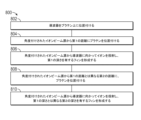
チャンバの処理空間内のペデスタル上に基板を位置付けることと、
電極のセグメント化された表面に対向して前記ペデスタルを位置付けることであって、前記セグメント化された表面が、複数の角度付けされた表面を含む、前記ペデスタルを位置付けることと、
1つ又は複数の直角でない角度で、前記電極の前記セグメント化された表面から前記基板に向かって電子を投射して、前記基板上に角度付けされたフィンを形成することと
を含む、導波器製造方法。 A method for manufacturing a waveguide, the method comprising:
positioning the substrate on a pedestal within the processing space of the chamber;
positioning the pedestal opposite a segmented surface of an electrode, the segmented surface including a plurality of angled surfaces;
projecting electrons from the segmented surface of the electrode toward the substrate at one or more non-orthogonal angles to form angled fins on the substrate. How to make utensils.
第1の深さを有する角度付けされたフィンを形成することと
を更に含む、請求項1に記載の方法。 positioning the pedestal at a first distance from the segmented surface while projecting the electrons from the segmented surface;
2. The method of claim 1, further comprising forming angled fins having a first depth.
前記セグメント化された表面から電子を投射することと、
第2の深さを有する角度付けされたフィンを形成することと
を更に含む、請求項2に記載の方法。 positioning the pedestal at a second distance from the segmented surface;
projecting electrons from the segmented surface;
3. The method of claim 2, further comprising forming angled fins having a second depth.
チャンバの処理空間内のペデスタル上に基板を位置付けることと、
電極のセグメント化された表面に対向して前記ペデスタルを位置付けることあって、前記セグメント化された表面が、実質的に均一な形態を有する複数の角度付けされた表面を含む、前記ペデスタルを位置付けることと、
前記処理空間内にプラズマを生成することと、
1つ又は複数の直角でない角度で、前記電極の前記セグメント化された表面から前記基板に向かって電子を投射して、前記基板上に角度付けされたフィンを形成することと
を含む、導波器製造方法。 A method for manufacturing a waveguide, the method comprising:
positioning the substrate on a pedestal within the processing space of the chamber;
positioning the pedestal opposite a segmented surface of an electrode, the segmented surface including a plurality of angled surfaces having a substantially uniform configuration; and,
generating plasma within the processing space;
projecting electrons from the segmented surface of the electrode toward the substrate at one or more non-orthogonal angles to form angled fins on the substrate. How to make utensils.
第1のエッチングプロセス中に第1の深さを有する角度付けされたフィンを形成することと
を更に含む、請求項7に記載の方法。 positioning the pedestal at a first distance from the segmented surface while projecting the electrons from the segmented surface;
and forming angled fins having a first depth during the first etching process.
前記セグメント化された表面から電子を投射することと、
第2のエッチングプロセス中に第2の深さを有する角度付けされたフィンを形成することと
を更に含む、請求項8に記載の方法。 positioning the pedestal at a second distance from the segmented surface;
projecting electrons from the segmented surface;
9. The method of claim 8, further comprising forming angled fins having a second depth during a second etching process.
を更に含む、請求項7に記載の方法。 8. The method of claim 7, further comprising chucking the substrate to an electrode located on the pedestal.
チャンバの処理空間内のペデスタル上に基板を位置付けることと、
電極のセグメント化された表面に対向して前記ペデスタルを位置付けることあって、前記セグメント化された表面は、異なる形態を有し、かつ前記セグメント化された表面にわたるサイズ、形状、間隔、密度、又は分布のうちの少なくとも1つが異なる、複数の角度付けされた表面を含む、前記ペデスタルを位置付けることと、
前記処理空間内にプラズマを生成することと、
1つ又は複数の直角でない角度で、前記電極の前記セグメント化された表面から前記基板に向かって電子を投射して、前記基板上に角度付けされたフィンを形成することと
を含む、導波器製造方法。 A method for manufacturing a waveguide, the method comprising:
positioning the substrate on a pedestal within the processing space of the chamber;
positioning the pedestal opposite segmented surfaces of an electrode, the segmented surfaces having different morphologies and varying in size, shape, spacing, density, or density across the segmented surfaces; positioning the pedestal, the pedestal including a plurality of angled surfaces having different distributions;
generating plasma within the processing space;
projecting electrons from the segmented surface of the electrode toward the substrate at one or more non-orthogonal angles to form angled fins on the substrate. How to make utensils.
第1のエッチングプロセス中に第1の深さを有する角度付けされたフィンを形成することと
を更に含む、請求項12に記載の方法。 positioning the pedestal at a first distance from the segmented surface while projecting the electrons from the segmented surface;
and forming angled fins having a first depth during the first etching process.
前記セグメント化された表面から電子を投射することと、
第2のエッチングプロセス中に第2の深さを有する角度付けされたフィンを形成することと
を更に含む、請求項13に記載の方法。 positioning the pedestal at a second distance from the segmented surface;
projecting electrons from the segmented surface;
and forming angled fins having a second depth during a second etching process.
15. The method of claim 14, wherein the second depth is different than the first depth.
Applications Claiming Priority (5)
| Application Number | Priority Date | Filing Date | Title |
|---|---|---|---|
| US201862780805P | 2018-12-17 | 2018-12-17 | |
| US201862780792P | 2018-12-17 | 2018-12-17 | |
| US62/780,805 | 2018-12-17 | ||
| US62/780,792 | 2018-12-17 | ||
| PCT/US2019/066806 WO2020131848A1 (en) | 2018-12-17 | 2019-12-17 | Methods of optical device fabrication using an electron beam apparatus |
Publications (2)
| Publication Number | Publication Date |
|---|---|
| JP2022512491A JP2022512491A (en) | 2022-02-04 |
| JP7410951B2 true JP7410951B2 (en) | 2024-01-10 |
Family
ID=71071206
Family Applications (4)
| Application Number | Title | Priority Date | Filing Date |
|---|---|---|---|
| JP2021533442A Active JP7447118B2 (en) | 2018-12-17 | 2019-12-17 | Ion beam source for optical device manufacturing |
| JP2021533791A Active JP7410951B2 (en) | 2018-12-17 | 2019-12-17 | Method for manufacturing optical devices using electron beam equipment |
| JP2021533444A Pending JP2022515348A (en) | 2018-12-17 | 2019-12-17 | Manufacturing method of optical equipment using ion beam source |
| JP2021533786A Active JP7447119B2 (en) | 2018-12-17 | 2019-12-17 | Electron beam equipment for optical device manufacturing |
Family Applications Before (1)
| Application Number | Title | Priority Date | Filing Date |
|---|---|---|---|
| JP2021533442A Active JP7447118B2 (en) | 2018-12-17 | 2019-12-17 | Ion beam source for optical device manufacturing |
Family Applications After (2)
| Application Number | Title | Priority Date | Filing Date |
|---|---|---|---|
| JP2021533444A Pending JP2022515348A (en) | 2018-12-17 | 2019-12-17 | Manufacturing method of optical equipment using ion beam source |
| JP2021533786A Active JP7447119B2 (en) | 2018-12-17 | 2019-12-17 | Electron beam equipment for optical device manufacturing |
Country Status (7)
| Country | Link |
|---|---|
| US (5) | US10818472B2 (en) |
| EP (4) | EP3899614A4 (en) |
| JP (4) | JP7447118B2 (en) |
| KR (4) | KR20210094117A (en) |
| CN (4) | CN113227859B (en) |
| TW (5) | TWI730548B (en) |
| WO (4) | WO2020131848A1 (en) |
Families Citing this family (5)
| Publication number | Priority date | Publication date | Assignee | Title |
|---|---|---|---|---|
| US11333896B2 (en) * | 2018-06-28 | 2022-05-17 | Applied Materials, Inc. | Fabrication of diffraction gratings |
| KR102527761B1 (en) * | 2018-11-07 | 2023-04-28 | 어플라이드 머티어리얼스, 인코포레이티드 | Formation of Tilt Grids |
| US10991547B2 (en) * | 2019-09-25 | 2021-04-27 | Applied Materials, Inc. | Method and device for a carrier proximity mask |
| WO2022108986A1 (en) * | 2020-11-17 | 2022-05-27 | Applied Materials, Inc. | An optical device having structural and refractive index gradation, and method of fabricating the same |
| WO2023122426A1 (en) * | 2021-12-22 | 2023-06-29 | Applied Materials, Inc. | Method for forming multi-depth optical devices |
Citations (5)
| Publication number | Priority date | Publication date | Assignee | Title |
|---|---|---|---|---|
| US20080317968A1 (en) | 2005-04-25 | 2008-12-25 | Varian Semiconductor Equipment Associates, Inc. | Tilted plasma doping |
| WO2013118517A1 (en) | 2012-02-10 | 2013-08-15 | 国立大学法人東北大学 | Electron beam generating appartus, electron beam irradaition apparatus, multi-electron beam irradiation apparatus, electron beam exposure apparatus, electron beam irradiation method, and manufacture method |
| US20140353141A1 (en) | 2011-10-19 | 2014-12-04 | Soochow University | Method for Manufacturing Holographic Blazed Grating |
| US20160035539A1 (en) | 2014-07-30 | 2016-02-04 | Lauri SAINIEMI | Microfabrication |
| JP2018037648A (en) | 2016-06-30 | 2018-03-08 | インフィネオン テクノロジーズ アーゲーInfineon Technologies Ag | Formation of electrode trench by using directed ion beam and semiconductor device with trench electrode structure |
Family Cites Families (61)
| Publication number | Priority date | Publication date | Assignee | Title |
|---|---|---|---|---|
| US4240448A (en) | 1978-08-21 | 1980-12-23 | Hauni-Werke Korber & Co. Kg | Apparatus for increasing the permeability of wrapping material for rod-shaped smokers' products |
| US5116461A (en) * | 1991-04-22 | 1992-05-26 | Motorola, Inc. | Method for fabricating an angled diffraction grating |
| US5375456A (en) | 1993-11-18 | 1994-12-27 | Trw Vehicle Safety Systems Inc. | Leak testing apparatus and method |
| JP3768547B2 (en) | 1993-12-17 | 2006-04-19 | キヤノン株式会社 | Double-sided film formation method |
| US5981899A (en) * | 1997-01-17 | 1999-11-09 | Balzers Aktiengesellschaft | Capacitively coupled RF-plasma reactor |
| US6211628B1 (en) * | 1997-08-02 | 2001-04-03 | Corning Incorporated | System for controlling the position of an electron beam in a cathode ray tube and method thereof |
| KR19990047679A (en) | 1997-12-05 | 1999-07-05 | 박호군 | Apparatus for Surface Treatment of Materials Using Ion Beams |
| JP4283432B2 (en) | 2000-11-06 | 2009-06-24 | 株式会社日立製作所 | Sample preparation equipment |
| US7546016B2 (en) * | 2001-06-28 | 2009-06-09 | E-Beam & Light, Inc. | Optical elements formed by inducing changes in the index of refraction by utilizing electron beam radiation |
| GB2386247B (en) * | 2002-01-11 | 2005-09-07 | Applied Materials Inc | Ion beam generator |
| DE10234614B3 (en) | 2002-07-24 | 2004-03-04 | Fractal Ag | Process for processing carrier material by heavy ion radiation and subsequent etching process |
| JP2004363085A (en) * | 2003-05-09 | 2004-12-24 | Ebara Corp | Inspection apparatus by charged particle beam and method for manufacturing device using inspection apparatus |
| KR20060003591A (en) * | 2004-07-07 | 2006-01-11 | 주성엔지니어링(주) | Plasma process apparatus which comprises plasma electrode having several protrusions |
| US7780821B2 (en) | 2004-08-02 | 2010-08-24 | Seagate Technology Llc | Multi-chamber processing with simultaneous workpiece transport and gas delivery |
| KR100851901B1 (en) * | 2005-01-07 | 2008-08-13 | 삼성전자주식회사 | Apparatus for extraction ion beam |
| KR100702010B1 (en) | 2005-03-07 | 2007-03-30 | 삼성전자주식회사 | Reflector, substrate processing apparatus employing the same, and substrate processing methods using the same |
| WO2007067296A2 (en) * | 2005-12-02 | 2007-06-14 | Alis Corporation | Ion sources, systems and methods |
| US8466953B2 (en) | 2006-06-02 | 2013-06-18 | Nokia Corporation | Stereoscopic exit pupil expander display |
| JP2008117753A (en) | 2006-10-12 | 2008-05-22 | Tdk Corp | Ion gun, ion beam etching device, ion beam etching equipment, etching method and manufacturing method of magnetic recording medium |
| JP5055011B2 (en) | 2007-04-23 | 2012-10-24 | 株式会社日立ハイテクノロジーズ | Ion source |
| US7723699B2 (en) * | 2007-06-26 | 2010-05-25 | Varian Semiconductor Equipment Associates, Inc. | Cathode having electron production and focusing grooves, ion source and related method |
| US20090084501A1 (en) * | 2007-09-27 | 2009-04-02 | Tokyo Electron Limited | Processing system for producing a negative ion plasma |
| US7915597B2 (en) * | 2008-03-18 | 2011-03-29 | Axcelis Technologies, Inc. | Extraction electrode system for high current ion implanter |
| US20090236214A1 (en) * | 2008-03-20 | 2009-09-24 | Karthik Janakiraman | Tunable ground planes in plasma chambers |
| US8986558B2 (en) | 2008-09-01 | 2015-03-24 | Japan Science And Technology Agency | Plasma etching method, plasma etching device, and method for producing photonic crystal |
| WO2011007546A1 (en) | 2009-07-16 | 2011-01-20 | キヤノンアネルバ株式会社 | Ion-beam generating device, substrate processing device, and manufacturing method of electronic device |
| US20110065282A1 (en) | 2009-09-11 | 2011-03-17 | General Electric Company | Apparatus and methods to form a patterned coating on an oled substrate |
| US8173527B2 (en) | 2009-10-19 | 2012-05-08 | Varian Semiconductor Equipment Associates, Inc. | Stepped masking for patterned implantation |
| US8129695B2 (en) * | 2009-12-28 | 2012-03-06 | Varian Semiconductor Equipment Associates, Inc. | System and method for controlling deflection of a charged particle beam within a graded electrostatic lens |
| CN108425098A (en) | 2011-12-21 | 2018-08-21 | 应用材料公司 | System and method for handling substrate |
| US8984451B2 (en) * | 2013-02-22 | 2015-03-17 | Aselta Nanographics | Free form fracturing method for electronic or optical lithography |
| US9288889B2 (en) * | 2013-03-13 | 2016-03-15 | Varian Semiconductor Equipment Associates, Inc. | Apparatus and techniques for energetic neutral beam processing |
| US9245761B2 (en) | 2013-04-05 | 2016-01-26 | Lam Research Corporation | Internal plasma grid for semiconductor fabrication |
| JP6348321B2 (en) * | 2013-05-17 | 2018-06-27 | キヤノンアネルバ株式会社 | Etching device |
| US9017526B2 (en) | 2013-07-08 | 2015-04-28 | Lam Research Corporation | Ion beam etching system |
| TWI690968B (en) * | 2014-03-07 | 2020-04-11 | 美商應用材料股份有限公司 | Grazing angle plasma processing for modifying a substrate surface |
| US9287123B2 (en) * | 2014-04-28 | 2016-03-15 | Varian Semiconductor Equipment Associates, Inc. | Techniques for forming angled structures for reduced defects in heteroepitaxy of semiconductor films |
| US9534289B2 (en) * | 2014-06-18 | 2017-01-03 | Applied Materials, Inc. | Plasma process chambers employing distribution grids having focusing surfaces thereon enabling angled fluxes to reach a substrate, and related methods |
| US9343312B2 (en) | 2014-07-25 | 2016-05-17 | Taiwan Semiconductor Manufacturing Company, Ltd. | High temperature intermittent ion implantation |
| US9304235B2 (en) * | 2014-07-30 | 2016-04-05 | Microsoft Technology Licensing, Llc | Microfabrication |
| US9406535B2 (en) * | 2014-08-29 | 2016-08-02 | Lam Research Corporation | Ion injector and lens system for ion beam milling |
| US10825652B2 (en) | 2014-08-29 | 2020-11-03 | Lam Research Corporation | Ion beam etch without need for wafer tilt or rotation |
| US9659797B1 (en) * | 2014-09-17 | 2017-05-23 | Sandia Corporation | Wafer scale oblique angle plasma etching |
| US9536748B2 (en) * | 2014-10-21 | 2017-01-03 | Lam Research Corporation | Use of ion beam etching to generate gate-all-around structure |
| KR101943553B1 (en) * | 2014-11-25 | 2019-04-18 | 삼성전자주식회사 | Method of forming a pattern using ion beams of bilateral symmetry, method of forming a magnetic memory device using the same, and ion beam apparatus generation ion beams of bilateral symmetry |
| JP6584787B2 (en) * | 2015-02-13 | 2019-10-02 | 株式会社日立ハイテクノロジーズ | Plasma ion source and charged particle beam device |
| US10475626B2 (en) * | 2015-03-17 | 2019-11-12 | Applied Materials, Inc. | Ion-ion plasma atomic layer etch process and reactor |
| US9478399B2 (en) | 2015-03-27 | 2016-10-25 | Varian Semiconductor Equipment Associates, Inc. | Multi-aperture extraction system for angled ion beam |
| US9697988B2 (en) * | 2015-10-14 | 2017-07-04 | Advanced Ion Beam Technology, Inc. | Ion implantation system and process |
| US9812349B2 (en) | 2015-12-01 | 2017-11-07 | Lam Research Corporation | Control of the incidence angle of an ion beam on a substrate |
| KR102341688B1 (en) * | 2016-01-26 | 2021-12-21 | 한국전자통신연구원 | Field emission device and x-ray emission source having the same |
| US10249495B2 (en) * | 2016-06-28 | 2019-04-02 | Applied Materials, Inc. | Diamond like carbon layer formed by an electron beam plasma process |
| US10141161B2 (en) | 2016-09-12 | 2018-11-27 | Varian Semiconductor Equipment Associates, Inc. | Angle control for radicals and reactive neutral ion beams |
| KR102233855B1 (en) | 2016-10-05 | 2021-03-29 | 매직 립, 인코포레이티드 | Fabrication of non-uniform diffraction gratings |
| KR20180065072A (en) * | 2016-12-06 | 2018-06-18 | 삼성전자주식회사 | Ion beam apparatus including slit structure for extracting ion beam, and etching method and method for forming magnetic memory device using the same |
| KR20180083027A (en) | 2017-01-11 | 2018-07-20 | 삼성전자주식회사 | Method of forming patterns of semiconductor device |
| US10544505B2 (en) * | 2017-03-24 | 2020-01-28 | Applied Materials, Inc. | Deposition or treatment of diamond-like carbon in a plasma reactor |
| US10222202B2 (en) | 2017-05-25 | 2019-03-05 | Varian Semiconductor Equipment Associates, Inc. | Three dimensional structure fabrication control using novel processing system |
| WO2018226481A1 (en) * | 2017-06-05 | 2018-12-13 | Applied Materials, Inc. | Waveguide fabrication with sacrificial sidewall spacers |
| KR102641752B1 (en) * | 2018-11-21 | 2024-03-04 | 삼성전자주식회사 | Gas injection module, substrate processing apparatus and method for manufacturing semiconductor device using the same |
| US20200321186A1 (en) * | 2019-04-02 | 2020-10-08 | Applied Materials, Inc. | Method and apparatus for angled etching |
-
2019
- 2019-12-17 CN CN201980083890.8A patent/CN113227859B/en active Active
- 2019-12-17 CN CN201980083747.9A patent/CN113196442A/en active Pending
- 2019-12-17 JP JP2021533442A patent/JP7447118B2/en active Active
- 2019-12-17 KR KR1020217022379A patent/KR20210094117A/en active Search and Examination
- 2019-12-17 KR KR1020217022376A patent/KR20210094116A/en unknown
- 2019-12-17 JP JP2021533791A patent/JP7410951B2/en active Active
- 2019-12-17 US US16/716,954 patent/US10818472B2/en active Active
- 2019-12-17 TW TW108146250A patent/TWI730548B/en active
- 2019-12-17 TW TW111101227A patent/TWI826899B/en active
- 2019-12-17 JP JP2021533444A patent/JP2022515348A/en active Pending
- 2019-12-17 EP EP19898594.7A patent/EP3899614A4/en active Pending
- 2019-12-17 TW TW108146266A patent/TWI755663B/en active
- 2019-12-17 EP EP19900535.6A patent/EP3899617B1/en active Active
- 2019-12-17 CN CN201980083897.XA patent/CN113242989A/en active Pending
- 2019-12-17 US US16/716,965 patent/US11462386B2/en active Active
- 2019-12-17 JP JP2021533786A patent/JP7447119B2/en active Active
- 2019-12-17 CN CN201980083749.8A patent/CN113196123A/en active Pending
- 2019-12-17 WO PCT/US2019/066806 patent/WO2020131848A1/en unknown
- 2019-12-17 TW TW108146252A patent/TWI708082B/en active
- 2019-12-17 KR KR1020217022375A patent/KR20210094115A/en active Search and Examination
- 2019-12-17 WO PCT/US2019/066797 patent/WO2020131843A1/en unknown
- 2019-12-17 WO PCT/US2019/066789 patent/WO2020131839A1/en unknown
- 2019-12-17 US US16/717,400 patent/US11640898B2/en active Active
- 2019-12-17 WO PCT/US2019/066780 patent/WO2020131831A1/en unknown
- 2019-12-17 US US16/717,211 patent/US11810755B2/en active Active
- 2019-12-17 EP EP19900534.9A patent/EP3899615A4/en active Pending
- 2019-12-17 TW TW108146247A patent/TWI729629B/en active
- 2019-12-17 KR KR1020217022389A patent/KR20210094118A/en unknown
- 2019-12-17 EP EP19901270.9A patent/EP3900008A4/en active Pending
-
2020
- 2020-10-26 US US17/080,802 patent/US11430634B2/en active Active
Patent Citations (5)
| Publication number | Priority date | Publication date | Assignee | Title |
|---|---|---|---|---|
| US20080317968A1 (en) | 2005-04-25 | 2008-12-25 | Varian Semiconductor Equipment Associates, Inc. | Tilted plasma doping |
| US20140353141A1 (en) | 2011-10-19 | 2014-12-04 | Soochow University | Method for Manufacturing Holographic Blazed Grating |
| WO2013118517A1 (en) | 2012-02-10 | 2013-08-15 | 国立大学法人東北大学 | Electron beam generating appartus, electron beam irradaition apparatus, multi-electron beam irradiation apparatus, electron beam exposure apparatus, electron beam irradiation method, and manufacture method |
| US20160035539A1 (en) | 2014-07-30 | 2016-02-04 | Lauri SAINIEMI | Microfabrication |
| JP2018037648A (en) | 2016-06-30 | 2018-03-08 | インフィネオン テクノロジーズ アーゲーInfineon Technologies Ag | Formation of electrode trench by using directed ion beam and semiconductor device with trench electrode structure |
Also Published As
Similar Documents
| Publication | Publication Date | Title |
|---|---|---|
| JP7410951B2 (en) | Method for manufacturing optical devices using electron beam equipment | |
| US11404278B2 (en) | Optical component having variable depth gratings and method of formation | |
| TW202030766A (en) | Modulation of ion beam angle | |
| JP2023537511A (en) | Method for manufacturing an optical device structure | |
| TWI833729B (en) | Optical grating component and method of forming the same and augmented reality/virtual reality device |
Legal Events
| Date | Code | Title | Description |
|---|---|---|---|
| A621 | Written request for application examination |
Free format text: JAPANESE INTERMEDIATE CODE: A621 Effective date: 20221213 |
|
| TRDD | Decision of grant or rejection written | ||
| A01 | Written decision to grant a patent or to grant a registration (utility model) |
Free format text: JAPANESE INTERMEDIATE CODE: A01 Effective date: 20231128 |
|
| A61 | First payment of annual fees (during grant procedure) |
Free format text: JAPANESE INTERMEDIATE CODE: A61 Effective date: 20231222 |
|
| R150 | Certificate of patent or registration of utility model |
Ref document number: 7410951 Country of ref document: JP Free format text: JAPANESE INTERMEDIATE CODE: R150 |