JP7400995B2 - Power factor correcting switching power supply - Google Patents
Power factor correcting switching power supply Download PDFInfo
- Publication number
- JP7400995B2 JP7400995B2 JP2022572130A JP2022572130A JP7400995B2 JP 7400995 B2 JP7400995 B2 JP 7400995B2 JP 2022572130 A JP2022572130 A JP 2022572130A JP 2022572130 A JP2022572130 A JP 2022572130A JP 7400995 B2 JP7400995 B2 JP 7400995B2
- Authority
- JP
- Japan
- Prior art keywords
- circuit
- power factor
- switching
- power supply
- supply device
- Prior art date
- Legal status (The legal status is an assumption and is not a legal conclusion. Google has not performed a legal analysis and makes no representation as to the accuracy of the status listed.)
- Active
Links
- 239000003990 capacitor Substances 0.000 claims description 144
- 238000001514 detection method Methods 0.000 claims description 10
- 238000010586 diagram Methods 0.000 description 28
- 230000000694 effects Effects 0.000 description 10
- 230000001629 suppression Effects 0.000 description 6
- 206010014357 Electric shock Diseases 0.000 description 4
- 238000009499 grossing Methods 0.000 description 2
- 238000012986 modification Methods 0.000 description 2
- 230000004048 modification Effects 0.000 description 2
- 230000002159 abnormal effect Effects 0.000 description 1
- 238000005516 engineering process Methods 0.000 description 1
- 230000004043 responsiveness Effects 0.000 description 1
- 238000004904 shortening Methods 0.000 description 1
- 239000013589 supplement Substances 0.000 description 1
Images


Classifications
-
- H—ELECTRICITY
- H02—GENERATION; CONVERSION OR DISTRIBUTION OF ELECTRIC POWER
- H02M—APPARATUS FOR CONVERSION BETWEEN AC AND AC, BETWEEN AC AND DC, OR BETWEEN DC AND DC, AND FOR USE WITH MAINS OR SIMILAR POWER SUPPLY SYSTEMS; CONVERSION OF DC OR AC INPUT POWER INTO SURGE OUTPUT POWER; CONTROL OR REGULATION THEREOF
- H02M1/00—Details of apparatus for conversion
- H02M1/42—Circuits or arrangements for compensating for or adjusting power factor in converters or inverters
- H02M1/4208—Arrangements for improving power factor of AC input
- H02M1/4225—Arrangements for improving power factor of AC input using a non-isolated boost converter
-
- H—ELECTRICITY
- H02—GENERATION; CONVERSION OR DISTRIBUTION OF ELECTRIC POWER
- H02M—APPARATUS FOR CONVERSION BETWEEN AC AND AC, BETWEEN AC AND DC, OR BETWEEN DC AND DC, AND FOR USE WITH MAINS OR SIMILAR POWER SUPPLY SYSTEMS; CONVERSION OF DC OR AC INPUT POWER INTO SURGE OUTPUT POWER; CONTROL OR REGULATION THEREOF
- H02M1/00—Details of apparatus for conversion
- H02M1/44—Circuits or arrangements for compensating for electromagnetic interference in converters or inverters
-
- H—ELECTRICITY
- H02—GENERATION; CONVERSION OR DISTRIBUTION OF ELECTRIC POWER
- H02M—APPARATUS FOR CONVERSION BETWEEN AC AND AC, BETWEEN AC AND DC, OR BETWEEN DC AND DC, AND FOR USE WITH MAINS OR SIMILAR POWER SUPPLY SYSTEMS; CONVERSION OF DC OR AC INPUT POWER INTO SURGE OUTPUT POWER; CONTROL OR REGULATION THEREOF
- H02M1/00—Details of apparatus for conversion
- H02M1/12—Arrangements for reducing harmonics from ac input or output
- H02M1/123—Suppression of common mode voltage or current
-
- H—ELECTRICITY
- H02—GENERATION; CONVERSION OR DISTRIBUTION OF ELECTRIC POWER
- H02M—APPARATUS FOR CONVERSION BETWEEN AC AND AC, BETWEEN AC AND DC, OR BETWEEN DC AND DC, AND FOR USE WITH MAINS OR SIMILAR POWER SUPPLY SYSTEMS; CONVERSION OF DC OR AC INPUT POWER INTO SURGE OUTPUT POWER; CONTROL OR REGULATION THEREOF
- H02M1/00—Details of apparatus for conversion
- H02M1/42—Circuits or arrangements for compensating for or adjusting power factor in converters or inverters
- H02M1/4208—Arrangements for improving power factor of AC input
- H02M1/4233—Arrangements for improving power factor of AC input using a bridge converter comprising active switches
-
- H—ELECTRICITY
- H02—GENERATION; CONVERSION OR DISTRIBUTION OF ELECTRIC POWER
- H02M—APPARATUS FOR CONVERSION BETWEEN AC AND AC, BETWEEN AC AND DC, OR BETWEEN DC AND DC, AND FOR USE WITH MAINS OR SIMILAR POWER SUPPLY SYSTEMS; CONVERSION OF DC OR AC INPUT POWER INTO SURGE OUTPUT POWER; CONTROL OR REGULATION THEREOF
- H02M7/00—Conversion of ac power input into dc power output; Conversion of dc power input into ac power output
- H02M7/02—Conversion of ac power input into dc power output without possibility of reversal
- H02M7/04—Conversion of ac power input into dc power output without possibility of reversal by static converters
- H02M7/12—Conversion of ac power input into dc power output without possibility of reversal by static converters using discharge tubes with control electrode or semiconductor devices with control electrode
Description
本発明は、交流電圧を入力し直流電圧を出力する電源装置において、力率を改善するスイッチング電源装置に関する。 The present invention relates to a switching power supply device that improves the power factor in a power supply device that inputs an AC voltage and outputs a DC voltage.
一般にPFCコンバータと呼ばれる力率改善スイッチング電源装置は、交流ラインを入力、直流ラインを出力とするコンバータであり、整流平滑動作による力率の低下を改善するために電源装置の交流入力部に設けられる。 A power factor correction switching power supply device, generally called a PFC converter, is a converter that uses an AC line as an input and a DC line as an output, and is installed at the AC input section of the power supply device in order to improve the decrease in power factor caused by rectification and smoothing operation. .
このような力率改善スイッチング電源装置では、電磁妨害波の発生を抑制するために、インピーダンスを備えた大型のコモンモードチョークコイルを多数使用する必要があるので、EMIノイズ対策回路となるフィルタ回路は大型かつコスト高になり、力率改善スイッチング電源装置自体が大型で高コストになるという問題がある。 In such a power factor correction switching power supply, it is necessary to use a large number of large common mode choke coils with impedance in order to suppress the generation of electromagnetic interference waves, so a filter circuit that serves as an EMI noise countermeasure circuit is required. There is a problem that the power factor correction switching power supply device itself is large and expensive.
特に、ダイオードブリッジ回路を備えないブリッジレスPFCコンバータでは、出力となる直流ラインの電位は、アース電位に対して実質的にフローティングとなるため、大きなコモンモードノイズが発生して、スイッチング動作に起因する電磁雑音が交流の入力ラインに重畳され、その結果、電磁妨害波(EMIノイズ)が発生し、他の回路が電磁干渉を受けるおそれがある。 In particular, in a bridgeless PFC converter that does not have a diode bridge circuit, the potential of the output DC line is essentially floating with respect to the ground potential, which generates large common mode noise, which is caused by switching operations. Electromagnetic noise is superimposed on the AC input line, and as a result, electromagnetic interference waves (EMI noise) are generated, and other circuits may be subject to electromagnetic interference.
小型かつ低コストにEMIノイズを抑制する回路構成のブリッジレスPFCコンバータとしては特許文献1が示されている。EMIノイズを低減させるには、ノイズ対策回路となるフィルタキャパシタ(特許文献1に記載のC1及びC2)の容量を大きくする必要がある。しかし、これらフィルタキャパシタの容量を大きくしすぎると、出力電圧を安定化するためにスイッチング素子をフィードバック制御する回路の動作に影響を与えて、異常動作するおそれがある。
フィードバック制御を正常に行うためには、フィードバック制御回路の電子部品を適切に変更したり、利得や位相を再調整する必要があり、設計期間の長期化が問題となる。 In order to perform feedback control normally, it is necessary to appropriately change the electronic components of the feedback control circuit and readjust the gain and phase, which poses a problem of prolonging the design period.
また、フィルタキャパシタの容量を大きくすると、漏れ電流が増大し、感電の危険性が高まるので、安全性の確保においても問題となる。 Furthermore, increasing the capacity of the filter capacitor increases leakage current and increases the risk of electric shock, which also poses a problem in ensuring safety.
このように、力率改善スイッチング電源装置においては、EMIノイズの抑制とパワーインテグリティ(電源品質の確保)、そして力率改善スイッチング電源装置の設計期間の短縮などを同時に実現することが求められている。 In this way, power factor correcting switching power supplies are required to simultaneously suppress EMI noise, ensure power integrity (ensuring power supply quality), and shorten the design period for power factor correcting switching power supplies. .
そこで、本発明の目的は、フィードバック制御回路を備えた力率改善スイッチング電源装置において、コモンモードノイズがフィードバック制御に与える影響を抑制することにある。 SUMMARY OF THE INVENTION Therefore, an object of the present invention is to suppress the influence of common mode noise on feedback control in a power factor correcting switching power supply device including a feedback control circuit.
本開示の一例としての力率改善スイッチング電源装置は、交流入力ラインに接続される力率改善回路を備え、前記力率改善回路は、インダクタと、前記インダクタにスイッチング電流を流すスイッチング回路と、前記インダクタに接続されて電圧を平滑する第1出力コンデンサと、前記第1出力コンデンサの電圧を検出する出力電圧検出回路と、前記交流入力ラインに流れる電流波形の概形が前記交流入力ラインの電圧波形の概形に追従するように、前記交流入力ライン間の電圧の変化に応じて前記スイッチング回路を制御し、かつ、前記第1出力コンデンサの出力電圧が所定電圧となるように前記スイッチング回路を制御するフィードバック制御回路を備えた力率改善制御回路と、前記交流入力ライン間に接続され、互いに直列接続された2つのコンデンサで構成される第1ハーフブリッジコンデンサ回路と、前記第1出力コンデンサより負荷側の直流出力ライン間に接続され、互いに直列接続された2つのコンデンサで構成される第2ハーフブリッジコンデンサ回路と、前記第1出力コンデンサと前記第2ハーフブリッジコンデンサ回路との間又は前記第1ハーフブリッジコンデンサ回路と前記スイッチング回路との間に設けられたコモンモードチョークコイルと、前記第1ハーフブリッジコンデンサ回路の中点と前記第2ハーフブリッジコンデンサ回路の中点とを電気的に接続して、アースやフレームグランドとは異なる電位のコモンモードノイズを平衡化するノイズ平衡回路を構成する電気経路と、を有する。 A power factor correction switching power supply device as an example of the present disclosure includes a power factor correction circuit connected to an AC input line, and the power factor correction circuit includes an inductor, a switching circuit that causes a switching current to flow through the inductor, and the power factor correction circuit that is connected to an AC input line. a first output capacitor connected to an inductor to smooth the voltage; an output voltage detection circuit that detects the voltage of the first output capacitor; and a voltage waveform of the AC input line whose approximate shape is the current waveform flowing through the AC input line. controlling the switching circuit in accordance with changes in voltage between the AC input lines so as to follow a general shape of the AC input line, and controlling the switching circuit so that the output voltage of the first output capacitor becomes a predetermined voltage. a first half-bridge capacitor circuit connected between the AC input lines and comprising two capacitors connected in series; and a power factor correction control circuit equipped with a feedback control circuit to a second half-bridge capacitor circuit connected between the side DC output lines and configured of two capacitors connected in series with each other; A common mode choke coil provided between a half-bridge capacitor circuit and the switching circuit, and a midpoint of the first half-bridge capacitor circuit and a midpoint of the second half-bridge capacitor circuit are electrically connected to each other. , and an electrical path constituting a noise balancing circuit that balances common mode noise at a potential different from that of earth or frame ground.
この構成により、前記ノイズ平衡回路は、コモンモードノイズが前記フィードバック制御回路に与える影響を抑制することを特徴とする。 With this configuration, the noise balancing circuit is characterized in that it suppresses the influence of common mode noise on the feedback control circuit.
本発明によれば、力率改善スイッチング電源回路において、コモンモードノイズがフィードバック制御に与える影響を抑制できる。 According to the present invention, it is possible to suppress the influence of common mode noise on feedback control in a power factor correcting switching power supply circuit.
以降、図を参照して幾つかの具体的な例を挙げて、本発明を実施するための複数の形態を示す。各図中には同一箇所に同一符号を付している。要点の説明又は理解の容易性を考慮して、実施形態を説明の便宜上、複数の実施形態に分けて示すが、異なる実施形態で示した構成の部分的な置換又は組み合わせは可能である。第2の実施形態以降では第1の実施形態と共通の事柄についての記述を省略し、異なる点についてのみ説明する。特に、同様の構成による同様の作用効果については実施形態毎には逐次言及しない。 Hereinafter, a plurality of embodiments for carrying out the present invention will be described with reference to the drawings and some specific examples. In each figure, the same parts are given the same reference numerals. In consideration of easiness of explanation or understanding of the main points, the embodiment is shown divided into a plurality of embodiments for convenience of explanation, but it is possible to partially replace or combine the configurations shown in different embodiments. In the second embodiment and subsequent embodiments, descriptions of matters common to the first embodiment will be omitted, and only differences will be described. In particular, similar effects due to similar configurations will not be mentioned for each embodiment.
《第1の実施形態》
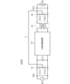
図1は第1の実施形態に係る力率改善スイッチング電源装置101の回路図である。この力率改善スイッチング電源装置101は、商用交流電源ACと負荷回路RLとの間に接続される回路である。また、この力率改善スイッチング電源装置101は交流入力ラインACLと直流出力ラインDCLとを備える。また、この力率改善スイッチング電源装置101は、力率改善回路10と、交流入力ラインACL間に接続され、互いに直列接続されたコンデンサC11,C12で構成される回路21(以降、「第1ハーフブリッジコンデンサ回路」という。)と、直流出力ラインDCL間に接続され、互いに直列接続されたコンデンサC21,C22で構成される回路22(以降、「第2ハーフブリッジコンデンサ回路」という。)と、力率改善回路10と第2ハーフブリッジコンデンサ回路22との間に設けられたコモンモードチョークコイル31と、を備える。《First embodiment》
FIG. 1 is a circuit diagram of a power factor correcting switching
力率改善スイッチング電源装置101は、第1ハーフブリッジコンデンサ回路21の中点と第2ハーフブリッジコンデンサ回路22の中点とを電気的に接続する電気経路1を備える。第1ハーフブリッジコンデンサ回路21の中点と第2ハーフブリッジコンデンサ回路の22中点とが電気経路1で電気的に接続されたことにより、アースやフレームグランドとは異なる電位のコモンモードノイズを平衡化するノイズ平衡回路が構成されている。より具体的には、コモンモードノイズは、比較的周波数が高く、位相も揃っていない。したがって、これらのコモンモードノイズが電気経路1に流れることによって互いに相殺され、コモンモードノイズは、平衡化される。
The power factor correcting switching
図2は、力率改善回路10内の具体的構成を示す、力率改善スイッチング電源装置101の回路図である。力率改善回路10は、交流入力ラインACLに直列接続されたインダクタL1,L2と、整流回路11と、整流回路11の出力電圧を比較的小さな時定数で平滑する第1出力コンデンサCo1と、整流回路11の出力電圧を検出する出力電圧検出回路13と、フィードバック制御回路14とを備える。
FIG. 2 is a circuit diagram of the power factor correction switching
整流回路11は、ダイオードD1,D2及びスイッチング回路12で構成されている。スイッチング回路12はスイッチ素子Q1,Q2で構成され、スイッチ素子Q1,Q2のスイッチングにより、インダクタL1,L2にスイッチング電流が流れる。フィードバック制御回路14は、交流入力ラインACLに流れる電流波形の概形が交流入力ラインACLの電圧波形の概形に追従するように、交流入力ライン間の電圧の変化に応じてスイッチング回路12を制御し、かつ、第1出力コンデンサCo1の出力電圧が所定電圧となるようにスイッチング回路12を制御する。
The
本実施形態によれば、次に挙げるような作用効果を奏する。 According to this embodiment, the following effects are achieved.
・第1ハーフブリッジコンデンサ回路21の中点と第2ハーフブリッジコンデンサ回路22の中点とを電気経路1で電気的に接続することにより、コモンモードノイズに対する平衡回路が形成されるので、フィードバック制御にほとんど影響を与えず、直流出力の電位変動およびコモンモードノイズを抑制できる。
- By electrically connecting the midpoint of the first half-
・第1ハーフブリッジコンデンサ回路の中点はアースやフレームグランドに接地されないので、この第1ハーフブリッジコンデンサ回路21に大容量のコンデンサを用いても、漏れ電流をあまり増大させることなく、EMIノイズを低減できる。
・Since the midpoint of the first half-bridge capacitor circuit is not grounded to the earth or frame ground, even if a large-capacity capacitor is used in the first half-
・電気経路1はアースやフレームグランドとは異なる電位に保たれるので、漏れ電流があまり増大せず、例えば1mA以下に抑えられ、感電の危険性が高まらない。
- Since the
・フィードバック制御回路14よりも後段にコモンモードチョークコイル31を接続したことにより、ハーフブリッジコンデンサに流れるコモンモード電流を低減でき、フィードバック回路へ与える影響を抑制できる。そのため、スイッチング電源装置の安定動作とEMIノイズの抑制を両立できる。これにより、フィードバック制御回路14の調整が不要になり、設計期間を短縮できる。
- By connecting the common
・これらの複合的な技術により、小型、低コストに、EMIノイズの抑制とパワーインテグリティ、そして設計期間短縮などを同時に両立する、力率改善スイッチング電源装置を実現できる。 - By combining these technologies, it is possible to realize a power factor correcting switching power supply device that is compact, low cost, and simultaneously achieves EMI noise suppression, power integrity, and shortened design time.
すなわち、力率改善スイッチング電源装置101の構成を備えることによって、スイッチング動作により発生するコモンモードノイズに対するノイズ平衡回路が形成され、直流出力の電位変動およびコモンモードノイズが抑制され、かつ、フィルタキャパシタの容量を大きくしてもフィードバック制御がほとんど影響を受けることがなく、かつ、漏れ電流の増大が少ない力率改善スイッチング電源装置が得られる。さらに、力率改善スイッチング電源装置101の構成を備えることによって、フィルタキャパシタの容量を大きくしてもフィードバック制御がほとんど影響を受けないことや漏洩電流の増大が少ないことにより再設計などが不要となり、設計期間の大幅な短縮が可能となる。また、このことにより、EMIノイズの抑制とパワーインテグリティ(電源品質の確保)、そして力率改善スイッチング電源装置の設計期間短縮化が同時に実現できる。
That is, by providing the configuration of the power factor correcting switching
《第2の実施形態》
第2の実施形態では入力コンデンサを備える力率改善スイッチング電源装置及び第2出力コンデンサを備える力率改善スイッチング電源装置について例示する。《Second embodiment》
In the second embodiment, a power factor improving switching power supply device including an input capacitor and a power factor improving switching power supply device including a second output capacitor will be exemplified.
図3は第2の実施形態に係る力率改善スイッチング電源装置102Aの回路図である。この力率改善スイッチング電源装置102Aは、商用交流電源ACと負荷回路RLとの間に接続される回路である。この力率改善スイッチング電源装置102Aは交流入力ラインACLと直流出力ラインDCLとを備える。この力率改善スイッチング電源装置102Aは、力率改善回路10と、第1ハーフブリッジコンデンサ回路21と、第2ハーフブリッジコンデンサ回路22と、コモンモードチョークコイル31と、を備える。力率改善スイッチング電源装置102Aは、第1ハーフブリッジコンデンサ回路21に並列接続された入力コンデンサC1を更に備える。
FIG. 3 is a circuit diagram of a power factor correcting switching
このように入力コンデンサC1を備えることにより、入力コンデンサC1によるEMIノイズの低減効果が向上する。 By providing the input capacitor C1 in this manner, the effect of reducing EMI noise by the input capacitor C1 is improved.
図4は第2の実施形態に係る別の力率改善スイッチング電源装置102Bの回路図である。この力率改善スイッチング電源装置102Bは、商用交流電源ACと負荷回路RLとの間に接続される回路である。この力率改善スイッチング電源装置102Bは交流入力ラインACLと直流出力ラインDCLとを備える。この力率改善スイッチング電源装置102Bは、力率改善回路10と、第1ハーフブリッジコンデンサ回路21と、第2ハーフブリッジコンデンサ回路22と、コモンモードチョークコイル31と、を備える。力率改善スイッチング電源装置102Bは、第2ハーフブリッジコンデンサ回路22に並列接続された第2出力コンデンサCo2を備える。
FIG. 4 is a circuit diagram of another power factor correction switching
このように第2出力コンデンサCo2を備えることにより、負荷回路RLから流入するノイズを抑制する効果が向上する。 By providing the second output capacitor Co2 in this way, the effect of suppressing noise flowing from the load circuit RL is improved.
《第3の実施形態》
第3の実施形態では、ACラインフィルタ回路を備える力率改善スイッチング電源装置103について例示する。《Third embodiment》
In the third embodiment, a power factor correction switching
図5は第3の実施形態に係る力率改善スイッチング電源装置103の回路図である。この力率改善スイッチング電源装置103は、商用交流電源ACと負荷回路RLとの間に接続される回路である。この力率改善スイッチング電源装置103は、力率改善回路10と、第1ハーフブリッジコンデンサ回路21と、第2ハーフブリッジコンデンサ回路22と、力率改善回路10と第2ハーフブリッジコンデンサ回路22との間に設けられたコモンモードチョークコイル31と、を備える。
FIG. 5 is a circuit diagram of a power factor correcting switching
本実施形態の力率改善スイッチング電源装置103は、交流入力ラインACLと第1ハーフブリッジコンデンサ回路21との間に接続されたACラインフィルタ回路4を備える。
The power factor correction switching
ACラインフィルタ回路4は、ACライン間に並列接続されたコンデンサC41,C42,C43と、ACライン間に接続されたコンデンサC44,C45によるラインバイパスコンデンサ回路と、コモンモードチョークコイル41,42とを備える。ラインバイパスコンデンサ回路の中点はアースやフレームグランドに接地されている。
The AC
このようにACラインフィルタ回路4を備えることにより、EMIノイズ低減効果がさらに向上する。例えば、150kHzから30MHzの周波数帯のうち低い周波数帯である150kHz帯のコモンモードノイズの抑制を行う。
By providing the AC
ラインバイパスコンデンサ回路を構成するコンデンサC44,C45を通してアースやフレームグランドに漏れ電流が流れるが、感電防止の面で、この漏れ電流は例えば1mA以下にする必要があるので、コンデンサC44,C45の容量はあまり大きくできない。そのため、ラインバイパスコンデンサ回路によるコモンノイズの抑制効果はあまり高くない。これに対し、第1ハーフブリッジコンデンサ回路21の中点と第2ハーフブリッジコンデンサ回路22の中点はアースやフレームグランドに接地されないので、漏れ電流による感電の問題がなく、コンデンサC11,C12,C21,C22の容量値は大きく設定できる。そのことにより、コモンモードノイズの抑制効果が高い。
Leakage current flows to the earth or frame ground through capacitors C44 and C45 that constitute the line bypass capacitor circuit, but in terms of preventing electric shock, this leakage current must be kept below 1 mA, for example, so the capacitance of capacitors C44 and C45 is It can't be made too big. Therefore, the effect of suppressing common noise by the line bypass capacitor circuit is not very high. On the other hand, since the midpoint of the first half-
また、コモンモードチョークコイル31を構成するコイルL11,L12の自己インダクタンス値は、ACラインフィルタ用コモンモードチョークコイル41,42を構成するコイルL41,L42,L43,L44のうち最も高い自己インダクタンス値よりも小さい。例えばコイルL41,L42,L43,L44のインダクタンスは1~3mH(数mHオーダー)であるのに対し、コイルL11,L12のインダクタンスは500μH(数百μHオーダー)である。このことより、機器の小型化や低コスト化が可能になる。
Further, the self-inductance value of the coils L11 and L12 that constitute the common
《第4の実施形態》
第4の実施形態では、コモンモードチョークコイルと力率改善回路との接続関係がこれまでに示した例とは異なる力率改善スイッチング電源装置について例示する。《Fourth embodiment》
In the fourth embodiment, a power factor correction switching power supply device in which the connection relationship between the common mode choke coil and the power factor correction circuit is different from the examples shown above will be exemplified.
図6は第4の実施形態に係る力率改善スイッチング電源装置104Aの回路図である。この力率改善スイッチング電源装置104Aは、商用交流電源ACと負荷回路RLとの間に接続される回路である。この力率改善スイッチング電源装置104Aは交流入力ラインACLと直流出力ラインDCLとを備える。この力率改善スイッチング電源装置104Aは、力率改善回路10と、第1ハーフブリッジコンデンサ回路21と、第2ハーフブリッジコンデンサ回路22と、コモンモードチョークコイル31と、を備える。
FIG. 6 is a circuit diagram of a power factor correcting switching
第1の実施形態の力率改善スイッチング電源装置101では、図1に示したように、コモンモードチョークコイル31は、力率改善回路10と第2ハーフブリッジコンデンサ回路22との間に接続されていたが、本実施形態の力率改善スイッチング電源装置104Aでは、コモンモードチョークコイル31は、第1ハーフブリッジコンデンサ回路21と力率改善回路10との間に接続されている。
In the power factor correction switching
図7は第4の実施形態に係る別の力率改善スイッチング電源装置104Bの回路図である。この力率改善スイッチング電源装置104Bは、商用交流電源ACと負荷回路RLとの間に接続される回路である。この力率改善スイッチング電源装置104Bは、力率改善回路10と、第1ハーフブリッジコンデンサ回路21と、第2ハーフブリッジコンデンサ回路22と、力率改善回路10とコモンモードチョークコイル31と、を備える。
FIG. 7 is a circuit diagram of another power factor correction switching
図5に示したように、第3の実施形態の力率改善スイッチング電源装置103では、コモンモードチョークコイル31は、力率改善回路10と第2ハーフブリッジコンデンサ回路22との間に接続されていたが、第4の実施形態の力率改善スイッチング電源装置104Bでは、コモンモードチョークコイル31がACラインフィルタ回路4と力率改善回路10との間に接続されている。
As shown in FIG. 5, in the power factor correction switching
第4の実施形態でも第1の実施形態と同様の作用効果を奏する。 The fourth embodiment also has the same effects as the first embodiment.
《第5の実施形態》
第5の実施形態では、電気経路1にインピーダンス素子が接続された力率改善スイッチング電源装置について例示する。《Fifth embodiment》
In the fifth embodiment, a power factor correction switching power supply device in which an impedance element is connected to the
図8は第5の実施形態に係る力率改善スイッチング電源装置105A及び105Bの回路図である。これら力率改善スイッチング電源装置105A,105Bは、力率改善回路10と、第1ハーフブリッジコンデンサ回路21と、第2ハーフブリッジコンデンサ回路22と、コモンモードチョークコイル31と、を備える。また、第1ハーフブリッジコンデンサ回路21の中点と第2ハーフブリッジコンデンサ回路22の中点とを電気的に接続する電気経路1を備える。
FIG. 8 is a circuit diagram of power factor correcting switching
力率改善スイッチング電源装置105Aの電気経路1にはインピーダンス素子Z1が直列に接続されている。このインピーダンス素子Z1は少なくともインダクタンス成分又は抵抗成分を有する。
An impedance element Z1 is connected in series to the
力率改善スイッチング電源装置105Bの電気経路1とグランドとの間にはインピーダンス素子Z2が接続されている。このインピーダンス素子Z2は、少なくともキャパシタンス成分、インダクタンス成分又は抵抗成分を有する。この「グランド」は、アースやフレームグランドである。
An impedance element Z2 is connected between the
力率改善スイッチング電源装置105Aのように、電気経路1にインピーダンス素子Z1を直列接続することにより、コモンモードチョークコイル31によるコモンモードノイズの抑制効果が不十分であっても、インピーダンス素子Z1により、コモンモードノイズの抑制が補われる。つまり、第1ハーフブリッジコンデンサ回路21と第2ハーフブリッジコンデンサ回路22とが電気経路1を通して平衡するために移動するエネルギーを、インピーダンス素子Z1が熱として消費するので、それだけコモンモードノイズが抑制される。
By connecting the impedance element Z1 in series to the
力率改善スイッチング電源装置105Bでは、電気経路1とグランドとの間にインピーダンス素子Z2が接続されている。このインピーダンス素子Z2は少なくともキャパシタンス成分、インダクタンス成分又は抵抗成分を有する。
In the power factor correcting switching
このように、電気経路1とグランドとの間にインピーダンス素子Z2を接続することにより、コモンモードチョークコイル31によるコモンモードノイズの抑制効果が不十分であっても、インピーダンス素子Z2により、コモンモードノイズの抑制が補われる。つまり、第1ハーフブリッジコンデンサ回路21と第2ハーフブリッジコンデンサ回路22とが電気経路1を通して平衡するために流れる電流がインピーダンス素子Z2を通してグランドに流れる。この電流(漏れ電流)はラインバイパスコンデンサ回路を設けた場合に、そのラインバイパスコンデンサ回路からグランドに漏れる電流に比べれば少ない。そのため、漏洩電流が増大することはなく、かつ、フィードバック回路へ与える影響をより低減できる。
In this way, by connecting the impedance element Z2 between the
図9は第5の実施形態に係る更に別の力率改善スイッチング電源装置105C,105D,105Eの回路図である。これら力率改善スイッチング電源装置105C,105D,105Eでは、電気経路1とグランドとの間にインピーダンス素子Z2が接続されている。
FIG. 9 is a circuit diagram of yet another power factor correction switching
力率改善スイッチング電源装置105Cでは、電気経路1に対するインピーダンス素子Z2の接続点と第2ハーフブリッジコンデンサ回路22の中点との間にインピーダンス素子Z1が直列に接続されている。また、力率改善スイッチング電源装置105Dでは、電気経路1に対するインピーダンス素子Z2の接続点と第1ハーフブリッジコンデンサ回路21の中点との間にインピーダンス素子Z3が直列に接続されている。力率改善スイッチング電源装置105Eでは、電気経路1に対するインピーダンス素子Z2の接続点と第2ハーフブリッジコンデンサ回路22の中点との間にインピーダンス素子Z1が直列に接続されていて、電気経路1に対するインピーダンス素子Z2の接続点と第1ハーフブリッジコンデンサ回路21の中点との間にインピーダンス素子Z3が直列に接続されている。
In the power factor correcting switching
図9に示した各力率改善スイッチング電源装置105C,105D,105Eにおいて、インピーダンス素子Z1,Z3が抵抗又はインダクタであり、インピーダンス素子Z2がキャパシタであれば、これらインピーダンス素子によってローパスフィルタが構成される。また、インピーダンス素子Z1,Z3がキャパシタであり、インピーダンス素子Z2が抵抗又はインダクタであれば、これらインピーダンス素子によってハイパスフィルタが構成される。
In each of the power factor correcting switching
このように、電気経路1に周波数フィルタを接続することにより、直流出力ラインDCLへ出力されるコモンモード電圧の変動に対する、交流入力ラインACLのコモンモード電圧へのフィードバックの応答性を適宜定めることができる。
In this way, by connecting the frequency filter to the
《第6の実施形態》
第6の実施形態では、整流回路11及びスイッチング回路12の構成がこれまでに示した例とは異なる力率改善スイッチング電源装置について示す。《Sixth embodiment》
In the sixth embodiment, a power factor correcting switching power supply device in which the configurations of a
図10は第6の実施形態に係る力率改善スイッチング電源装置106Aの回路図である。この力率改善スイッチング電源装置106Aの力率改善回路10は、交流入力ラインACLに直列接続されたインダクタL1,L2と、整流回路11と、整流回路11の出力電圧を平滑する第1出力コンデンサCo1と、整流回路11の出力電圧を検出する出力電圧検出回路13と、フィードバック制御回路14とを備える。
FIG. 10 is a circuit diagram of a power factor correcting switching
整流回路11は、ダイオードD1,D2及びスイッチング回路12で構成されている。スイッチング回路12はスイッチ素子Q1,Q3で構成され、スイッチ素子Q1,Q3のスイッチングにより、インダクタL1,L2にスイッチング電流が流れる。その他の構成は第1の実施形態で図2に示した回路の構成と同様である。このように、ハイサイドとローサイドにスイッチ素子を設けてもよい。
The
図11は第6の実施形態に係る別の力率改善スイッチング電源装置106Bの回路図である。この力率改善スイッチング電源装置106Bの力率改善回路10の整流回路11は、スイッチ素子Q1,Q2,Q3,Q4で構成されている。これらスイッチ素子Q1,Q2,Q3,Q4のスイッチングにより、インダクタL1,L2にスイッチング電流が流れる。その他の構成は第1の実施形態で図2に示した回路の構成と同様である。このように、4つのスイッチ素子でブリッジ回路構成のスイッチング回路及び整流回路を構成してもよい。
FIG. 11 is a circuit diagram of another power factor correction switching
《第7の実施形態》
第7の実施形態では、インダクタの構成がこれまでに示した例とは異なる力率改善スイッチング電源装置について示す。《Seventh embodiment》
In the seventh embodiment, a power factor correction switching power supply device will be described in which the configuration of the inductor is different from the examples shown so far.
図12は第7の実施形態に係る力率改善スイッチング電源装置107の回路図である。力率改善回路10は、交流入力ラインACLに直列接続されたインダクタL1と、整流回路11と、整流回路11の出力電圧を平滑する第1出力コンデンサCo1と、整流回路11の出力電圧を検出する出力電圧検出回路13と、フィードバック制御回路14を備える。第1の実施形態において、図2に示した例とは異なり、交流入力ラインACLの一方のラインにのみインダクタL1が接続されている。その他の構成は第1の実施形態で示したとおりである。このように、スイッチング回路によってスイッチング電流が流れるインダクタは交流入力ラインACLの一方のラインにのみ設けてもよい。
FIG. 12 is a circuit diagram of a power factor correcting switching
《第8の実施形態》
第8の実施形態では、整流回路11及びスイッチング回路12の構成がこれまでに示した例とは異なる力率改善スイッチング電源装置について示す。《Eighth embodiment》
In the eighth embodiment, a power factor correction switching power supply device in which the configurations of a
図13は第8の実施形態に係る力率改善スイッチング電源装置108の回路図である。力率改善回路10は、交流入力ラインACLに直列接続されたインダクタL1A,L1Bと、整流回路11と、整流回路11の出力電圧を比較的小さな時定数で平滑する第1出力コンデンサCo1と、整流回路11の出力電圧を検出する出力電圧検出回路13と、フィードバック制御回路14を備える。
FIG. 13 is a circuit diagram of a power factor correcting switching
整流回路11はダイオードD1,D2,D3及びスイッチング回路12とで構成されている。スイッチング回路12はスイッチ素子Q1,Q2,Q3で構成されている。ダイオードD1とスイッチ素子Q1とは直列に接続されていて、その接続点にインダクタL1Aの一端が接続されている。ダイオードD3とスイッチ素子Q3とは直列に接続されていて、その接続点にインダクタL1Bの一端が接続されている。また、ダイオードD2とスイッチ素子Q2とは直列に接続されていて、その接続点は、インダクタL1A,L1Bが接続されていない側の交流入力ラインACLに接続されている。
The
フィードバック制御回路14は、スイッチ素子Q1及びスイッチ素子Q2のオンと、スイッチ素子Q3及びスイッチ素子Q2のオンと、を交互に行う。このように、インターリーブ動作する整流回路11を設けてもよい。
The
《第9の実施形態》
第9の実施形態では、ダイオードブリッジを備える力率改善スイッチング電源装置について例示する。《Ninth embodiment》
In the ninth embodiment, a power factor correction switching power supply device including a diode bridge will be exemplified.
図14は第9の実施形態に係る力率改善スイッチング電源装置109の回路図である。この力率改善スイッチング電源装置109は、商用交流電源ACと負荷回路RLとの間に接続される回路である。また、この力率改善スイッチング電源装置109は、交流入力ラインACL間に接続され、互いに直列接続された2つのコンデンサで構成される第1ハーフブリッジコンデンサ回路21と、直流出力ラインDCL間に接続され、互いに直列接続された2つのコンデンサで構成される第2ハーフブリッジコンデンサ回路22と、力率改善回路10と、コモンモードチョークコイル31と、ダイオードブリッジ回路DBと、を備える。
FIG. 14 is a circuit diagram of a power factor correcting switching
ダイオードブリッジ回路DBは交流入力ラインACLの交流電圧を全波整流する。力率改善回路10は、出力電圧検出回路13、第1出力コンデンサCo1、インダクタL5、スイッチ素子Q5、ダイオードD5及びコンデンサC5で構成されている。
The diode bridge circuit DB performs full-wave rectification of the AC voltage on the AC input line ACL. The power
インダクタL5、スイッチ素子Q5、ダイオードD5及びコンデンサC5によって昇圧チョッパー回路が構成されている。スイッチ素子Q5はスイッチング回路12を構成している。フィードバック制御回路14は、交流入力ラインACLに流れる電流波形の概形が交流入力ラインACLの電圧波形の概形に追従するように、交流入力ライン間の電圧の変化に応じてスイッチング回路12を制御し、かつ、第1出力コンデンサCo1の出力電圧が所定電圧となるようにスイッチング回路12を制御する。
A boost chopper circuit is configured by an inductor L5, a switching element Q5, a diode D5, and a capacitor C5. Switch element Q5 constitutes switching
本発明は、本実施形態に示すように、交流入力ラインACLとスイッチング回路12との間にダイオードブリッジ回路DBを備える回路にも適用できる。
The present invention can also be applied to a circuit including a diode bridge circuit DB between the AC input line ACL and the switching
最後に、本発明は上述した実施形態に限られるものではない。当業者によって適宜変形及び変更が可能である。本発明の範囲は、上述の実施形態ではなく、特許請求の範囲によって示される。さらに、本発明の範囲には、特許請求の範囲内と均等の範囲内での実施形態からの変形及び変更が含まれる。 Finally, the invention is not limited to the embodiments described above. Appropriate modifications and changes can be made by those skilled in the art. The scope of the invention is indicated by the claims rather than the embodiments described above. Furthermore, the scope of the present invention includes modifications and changes from the embodiments within the scope of the claims and equivalents.
AC…商用交流電源
ACL…交流入力ライン
C1…入力コンデンサ
C11,C12,C21,C22…コンデンサ
C41,C42,C43,C44,C45…コンデンサ
C5…コンデンサ
Co1…第1出力コンデンサ
Co2…第2出力コンデンサ
D1,D2,D3,D5…ダイオード
DB…ダイオードブリッジ回路
DCL…直流出力ライン
L1,L2…インダクタ
L11,L12…コイル
L1A,L1B…インダクタ
L41,L42,L43,L44…コイル
L5…インダクタ
Q1,Q2,Q3,Q4,Q5…スイッチ素子
RL…負荷回路
Z1,Z2,Z3…インピーダンス素子
1…電気経路
4…ACラインフィルタ回路
10…力率改善回路
11…整流回路
12…スイッチング回路
13…出力電圧検出回路
14…フィードバック制御回路
21…第1ハーフブリッジコンデンサ回路
22…第2ハーフブリッジコンデンサ回路
31…コモンモードチョークコイル
41,42…ACラインフィルタ用コモンモードチョークコイル
101,102A,102B,103,104A,104B,105A,105A,105B,105C,105D,105E,106A,106B,107,108,109…力率改善スイッチング電源装置AC...Commercial AC power supply ACL...AC input line C1...Input capacitor C11, C12, C21, C22...Capacitor C41, C42, C43, C44, C45...Capacitor C5...Capacitor Co1...First output capacitor Co2...Second output capacitor D1 , D2, D3, D5...Diode DB...Diode bridge circuit DCL...DC output line L1, L2...Inductor L11, L12...Coil L1A, L1B...Inductor L41, L42, L43, L44...Coil L5...Inductor Q1, Q2, Q3 , Q4, Q5... Switch element RL... Load circuit Z1, Z2, Z3...
Claims (11)
前記力率改善回路は、
インダクタと、
前記インダクタにスイッチング電流を流すスイッチング回路と、
前記インダクタに接続されて電圧を平滑する第1出力コンデンサと、
前記第1出力コンデンサの電圧を検出する出力電圧検出回路と、
前記交流入力ラインに流れる電流波形の概形が前記交流入力ラインの電圧波形の概形に追従するように、前記交流入力ライン間の電圧の変化に応じて前記スイッチング回路を制御し、かつ、前記第1出力コンデンサの出力電圧が所定電圧となるように前記スイッチング回路を制御するフィードバック制御回路と、を備えた、
力率改善スイッチング電源装置であって、
前記交流入力ライン間に接続され、互いに直列接続された2つのコンデンサで構成される第1ハーフブリッジコンデンサ回路と、
前記第1出力コンデンサより負荷側の直流出力ライン間に接続され、互いに直列接続された2つのコンデンサで構成される第2ハーフブリッジコンデンサ回路と、
前記第1出力コンデンサと前記第2ハーフブリッジコンデンサ回路との間又は前記第1ハーフブリッジコンデンサ回路と前記スイッチング回路との間に設けられたコモンモードチョークコイルと、
前記第1ハーフブリッジコンデンサ回路の中点と前記第2ハーフブリッジコンデンサ回路の中点とを電気的に接続しノイズ平衡回路を構成する電気経路と、
を有する、
力率改善スイッチング電源装置。 Equipped with a power factor correction circuit connected to the AC input line,
The power factor correction circuit is
an inductor;
a switching circuit that causes a switching current to flow through the inductor;
a first output capacitor connected to the inductor to smooth the voltage;
an output voltage detection circuit that detects the voltage of the first output capacitor;
controlling the switching circuit according to a change in voltage between the AC input lines so that the approximate shape of a current waveform flowing through the AC input line follows the approximate shape of a voltage waveform of the AC input line, and a feedback control circuit that controls the switching circuit so that the output voltage of the first output capacitor becomes a predetermined voltage;
A power factor correcting switching power supply device,
a first half-bridge capacitor circuit connected between the AC input lines and configured of two capacitors connected in series;
a second half-bridge capacitor circuit connected between the DC output lines on the load side of the first output capacitor and configured of two capacitors connected in series;
a common mode choke coil provided between the first output capacitor and the second half-bridge capacitor circuit or between the first half-bridge capacitor circuit and the switching circuit;
an electrical path that electrically connects a midpoint of the first half-bridge capacitor circuit and a midpoint of the second half-bridge capacitor circuit to configure a noise balancing circuit;
has,
Power factor corrected switching power supply.
前記力率改善回路は、 The power factor correction circuit is
インダクタと、 an inductor;
前記インダクタにスイッチング電流を流すスイッチング回路と、 a switching circuit that causes a switching current to flow through the inductor;
前記インダクタに接続されて電圧を平滑する第1出力コンデンサと、 a first output capacitor connected to the inductor to smooth the voltage;
前記第1出力コンデンサの電圧を検出する出力電圧検出回路と、 an output voltage detection circuit that detects the voltage of the first output capacitor;
前記交流入力ラインに流れる電流波形の概形が前記交流入力ラインの電圧波形の概形に追従するように、前記交流入力ライン間の電圧の変化に応じて前記スイッチング回路を制御し、かつ、前記第1出力コンデンサの出力電圧が所定電圧となるように前記スイッチング回路を制御するフィードバック制御回路と、を備えた、 controlling the switching circuit according to a change in voltage between the AC input lines so that the approximate shape of a current waveform flowing through the AC input line follows the approximate shape of a voltage waveform of the AC input line, and a feedback control circuit that controls the switching circuit so that the output voltage of the first output capacitor becomes a predetermined voltage;
力率改善スイッチング電源装置であって、 A power factor correcting switching power supply device,
前記交流入力ライン間に接続され、互いに直列接続された2つのコンデンサで構成される第1ハーフブリッジコンデンサ回路と、 a first half-bridge capacitor circuit connected between the AC input lines and configured of two capacitors connected in series;
前記第1出力コンデンサより負荷側の直流出力ライン間に接続され、互いに直列接続された2つのコンデンサで構成される第2ハーフブリッジコンデンサ回路と、 a second half-bridge capacitor circuit connected between the DC output lines on the load side of the first output capacitor and configured of two capacitors connected in series;
前記第1出力コンデンサと前記第2ハーフブリッジコンデンサ回路との間又は前記第1ハーフブリッジコンデンサ回路と前記スイッチング回路との間に設けられたコモンモードチョークコイルと、 a common mode choke coil provided between the first output capacitor and the second half-bridge capacitor circuit or between the first half-bridge capacitor circuit and the switching circuit;
前記第1ハーフブリッジコンデンサ回路の中点と前記第2ハーフブリッジコンデンサ回路の中点とを電気的に接続して、グランドとは異なる電位のコモンモードノイズを平衡化するノイズ平衡回路を構成する電気経路と、 An electric circuit that electrically connects the midpoint of the first half-bridge capacitor circuit and the midpoint of the second half-bridge capacitor circuit to form a noise balancing circuit that balances common mode noise at a potential different from ground. route and
を有する、 has,
力率改善スイッチング電源装置。 Power factor corrected switching power supply.
前記力率改善回路は、
インダクタと、
前記インダクタにスイッチング電流を流すスイッチング回路と、
前記インダクタに接続されて電圧を平滑する第1出力コンデンサと、
前記第1出力コンデンサの電圧を検出する出力電圧検出回路と、
前記交流入力ラインに流れる電流波形の概形が前記交流入力ラインの電圧波形の概形に追従するように、前記交流入力ライン間の電圧の変化に応じて前記スイッチング回路を制御し、かつ、前記第1出力コンデンサの出力電圧が所定電圧となるように前記スイッチング回路を制御するフィードバック制御回路と、を備えた、
力率改善スイッチング電源装置であって、
前記交流入力ライン間に接続され、互いに直列接続された2つのコンデンサで構成される第1ハーフブリッジコンデンサ回路と、
前記第1出力コンデンサより負荷側の直流出力ライン間に接続され、互いに直列接続された2つのコンデンサで構成される第2ハーフブリッジコンデンサ回路と、
前記第1出力コンデンサと前記第2ハーフブリッジコンデンサ回路との間又は前記第1ハーフブリッジコンデンサ回路と前記スイッチング回路との間に設けられたコモンモードチョークコイルと、
前記第1ハーフブリッジコンデンサ回路の中点と前記第2ハーフブリッジコンデンサ回路の中点とを電気的に接続して、グランドとは異なる電位のコモンモードノイズを平衡化するノイズ平衡回路を構成する電気経路と、
を有し、
前記ノイズ平衡回路は、コモンモードノイズが前記フィードバック制御回路に与える影響を抑制することを特徴とする、
力率改善スイッチング電源装置。 Equipped with a power factor correction circuit connected to the AC input line,
The power factor correction circuit is
an inductor;
a switching circuit that causes a switching current to flow through the inductor;
a first output capacitor connected to the inductor to smooth the voltage;
an output voltage detection circuit that detects the voltage of the first output capacitor;
controlling the switching circuit according to a change in voltage between the AC input lines so that the approximate shape of a current waveform flowing through the AC input line follows the approximate shape of a voltage waveform of the AC input line, and a feedback control circuit that controls the switching circuit so that the output voltage of the first output capacitor becomes a predetermined voltage;
A power factor correcting switching power supply device,
a first half-bridge capacitor circuit connected between the AC input lines and configured of two capacitors connected in series;
a second half-bridge capacitor circuit connected between the DC output lines on the load side of the first output capacitor and configured of two capacitors connected in series;
a common mode choke coil provided between the first output capacitor and the second half-bridge capacitor circuit or between the first half-bridge capacitor circuit and the switching circuit;
An electric circuit that electrically connects the midpoint of the first half-bridge capacitor circuit and the midpoint of the second half-bridge capacitor circuit to form a noise balancing circuit that balances common mode noise at a potential different from ground. route and
has
The noise balancing circuit is characterized in that it suppresses the influence of common mode noise on the feedback control circuit.
Power factor corrected switching power supply.
請求項1から3のいずれかに記載の力率改善スイッチング電源装置。 comprising a rectifier circuit connected between the AC input line and the switching circuit;
A power factor correction switching power supply device according to any one of claims 1 to 3 .
請求項4に記載の力率改善スイッチング電源装置。 The switching circuit is configured by a switching element that constitutes part or all of the rectifier circuit.
The power factor correcting switching power supply device according to claim 4 .
請求項1から5のいずれかに記載の力率改善スイッチング電源装置。 an input capacitor connected in parallel to the first half-bridge capacitor circuit;
A power factor correction switching power supply device according to any one of claims 1 to 5 .
請求項1から6のいずれかに記載の力率改善スイッチング電源装置。 a second output capacitor connected in parallel to the second half-bridge capacitor circuit;
A power factor correction switching power supply device according to any one of claims 1 to 6 .
請求項1から7のいずれかに記載の力率改善スイッチング電源装置。 an AC line filter circuit connected between the AC input line and the first half-bridge capacitor circuit;
A power factor correction switching power supply device according to any one of claims 1 to 7 .
前記コモンモードチョークコイルの自己インダクタンスは前記ACラインフィルタ用コモンモードチョークコイルのうち最も高い自己インダクタンスよりも小さい、
請求項8に記載の力率改善スイッチング電源装置。 The AC line filter circuit has an AC line filter common mode choke coil,
The self-inductance of the common mode choke coil is smaller than the highest self-inductance among the AC line filter common mode choke coils.
The power factor correcting switching power supply device according to claim 8 .
請求項1から9のいずれかに記載の力率改善スイッチング電源装置。 an impedance element connected in series to the electrical path and having an inductance component or a resistance component;
A power factor correction switching power supply device according to any one of claims 1 to 9 .
請求項1から10のいずれかに記載の力率改善スイッチング電源装置。 an impedance element connected between the electrical path and the ground and having a capacitance component, an inductance component, or a resistance component;
A power factor correction switching power supply device according to any one of claims 1 to 10 .
Applications Claiming Priority (3)
| Application Number | Priority Date | Filing Date | Title |
|---|---|---|---|
| JP2020210979 | 2020-12-21 | ||
| JP2020210979 | 2020-12-21 | ||
| PCT/JP2021/045426 WO2022138217A1 (en) | 2020-12-21 | 2021-12-10 | Power-factor improving switching power supply device |
Publications (3)
| Publication Number | Publication Date |
|---|---|
| JPWO2022138217A1 JPWO2022138217A1 (en) | 2022-06-30 |
| JPWO2022138217A5 JPWO2022138217A5 (en) | 2023-06-12 |
| JP7400995B2 true JP7400995B2 (en) | 2023-12-19 |
Family
ID=82159703
Family Applications (1)
| Application Number | Title | Priority Date | Filing Date |
|---|---|---|---|
| JP2022572130A Active JP7400995B2 (en) | 2020-12-21 | 2021-12-10 | Power factor correcting switching power supply |
Country Status (3)
| Country | Link |
|---|---|
| US (1) | US20230327545A1 (en) |
| JP (1) | JP7400995B2 (en) |
| WO (1) | WO2022138217A1 (en) |
Citations (2)
| Publication number | Priority date | Publication date | Assignee | Title |
|---|---|---|---|---|
| JP2018161024A (en) | 2017-03-21 | 2018-10-11 | 株式会社東芝 | Power conversion device and electric power conversion system |
| JP2019205317A (en) | 2018-05-25 | 2019-11-28 | 株式会社豊田自動織機 | On-vehicle electric power conversion device |
Family Cites Families (2)
| Publication number | Priority date | Publication date | Assignee | Title |
|---|---|---|---|---|
| JP2009095183A (en) * | 2007-10-11 | 2009-04-30 | Eta Electric Industry Co Ltd | Switching power-supply device |
| JP2016058495A (en) * | 2014-09-08 | 2016-04-21 | 株式会社東芝 | Common mode choke coil, common mode filter, and power converter |
-
2021
- 2021-12-10 JP JP2022572130A patent/JP7400995B2/en active Active
- 2021-12-10 WO PCT/JP2021/045426 patent/WO2022138217A1/en active Application Filing
-
2023
- 2023-06-13 US US18/334,154 patent/US20230327545A1/en active Pending
Patent Citations (2)
| Publication number | Priority date | Publication date | Assignee | Title |
|---|---|---|---|---|
| JP2018161024A (en) | 2017-03-21 | 2018-10-11 | 株式会社東芝 | Power conversion device and electric power conversion system |
| JP2019205317A (en) | 2018-05-25 | 2019-11-28 | 株式会社豊田自動織機 | On-vehicle electric power conversion device |
Also Published As
| Publication number | Publication date |
|---|---|
| WO2022138217A1 (en) | 2022-06-30 |
| JPWO2022138217A1 (en) | 2022-06-30 |
| US20230327545A1 (en) | 2023-10-12 |
Similar Documents
| Publication | Publication Date | Title |
|---|---|---|
| US7898827B2 (en) | Active EMI filtering using magnetic coupling cancellation | |
| US5530396A (en) | Damped EMI input filter power factor correction circuits | |
| KR20030002685A (en) | Active Common Mode EMI Filter for Eliminating Conducted Electromagnetic Interference | |
| JP7012232B2 (en) | Power circuit | |
| JP2023078385A (en) | Device for compensating for voltage or current | |
| CN102983737A (en) | Power factor correction apparatus and method | |
| JP7400995B2 (en) | Power factor correcting switching power supply | |
| CN110603724B (en) | Power supply circuit | |
| JP5030157B2 (en) | Switching power supply | |
| JP6239468B2 (en) | Medical equipment | |
| JP4879813B2 (en) | Switching power supply | |
| JPH10256859A (en) | Ac line filter | |
| WO2022138216A1 (en) | Switching power supply device | |
| WO2022138215A1 (en) | Switching power supply device | |
| JP2003153542A (en) | Active-type power factor improving circuit | |
| JP7012231B2 (en) | Power circuit | |
| JP3156440B2 (en) | Switching power supply | |
| JP2009148045A (en) | Leak current reducing device | |
| JPH1075565A (en) | Harmonic current suppressor for electronic apparatus | |
| KR102258197B1 (en) | Current compensation device | |
| JPH03186007A (en) | Line filter | |
| WO2024009489A1 (en) | Noise filter | |
| JPWO2022138217A5 (en) | ||
| JPH0265516A (en) | Line filter | |
| JP3203473B2 (en) | Power saving device |
Legal Events
| Date | Code | Title | Description |
|---|---|---|---|
| A521 | Request for written amendment filed |
Free format text: JAPANESE INTERMEDIATE CODE: A523 Effective date: 20230327 |
|
| A621 | Written request for application examination |
Free format text: JAPANESE INTERMEDIATE CODE: A621 Effective date: 20230327 |
|
| TRDD | Decision of grant or rejection written | ||
| A01 | Written decision to grant a patent or to grant a registration (utility model) |
Free format text: JAPANESE INTERMEDIATE CODE: A01 Effective date: 20231107 |
|
| A61 | First payment of annual fees (during grant procedure) |
Free format text: JAPANESE INTERMEDIATE CODE: A61 Effective date: 20231120 |
|
| R150 | Certificate of patent or registration of utility model |
Ref document number: 7400995 Country of ref document: JP Free format text: JAPANESE INTERMEDIATE CODE: R150 |