JP7384784B2 - Apparatus and method for improving uniformity in thermal chemical vapor deposition (CVD) - Google Patents
Apparatus and method for improving uniformity in thermal chemical vapor deposition (CVD) Download PDFInfo
- Publication number
- JP7384784B2 JP7384784B2 JP2020506157A JP2020506157A JP7384784B2 JP 7384784 B2 JP7384784 B2 JP 7384784B2 JP 2020506157 A JP2020506157 A JP 2020506157A JP 2020506157 A JP2020506157 A JP 2020506157A JP 7384784 B2 JP7384784 B2 JP 7384784B2
- Authority
- JP
- Japan
- Prior art keywords
- holes
- region
- substrate
- faceplate
- emissivity
- Prior art date
- Legal status (The legal status is an assumption and is not a legal conclusion. Google has not performed a legal analysis and makes no representation as to the accuracy of the status listed.)
- Active
Links
- 238000000034 method Methods 0.000 title description 27
- 238000005229 chemical vapour deposition Methods 0.000 title description 16
- 238000002230 thermal chemical vapour deposition Methods 0.000 title description 3
- 239000000758 substrate Substances 0.000 claims description 89
- 238000009826 distribution Methods 0.000 claims description 22
- 238000000151 deposition Methods 0.000 claims description 18
- 230000005855 radiation Effects 0.000 claims description 14
- 239000007789 gas Substances 0.000 description 55
- 230000008021 deposition Effects 0.000 description 16
- 239000000463 material Substances 0.000 description 12
- 239000011148 porous material Substances 0.000 description 10
- 229910052581 Si3N4 Inorganic materials 0.000 description 4
- XAGFODPZIPBFFR-UHFFFAOYSA-N aluminium Chemical compound [Al] XAGFODPZIPBFFR-UHFFFAOYSA-N 0.000 description 4
- 229910052782 aluminium Inorganic materials 0.000 description 4
- PMHQVHHXPFUNSP-UHFFFAOYSA-M copper(1+);methylsulfanylmethane;bromide Chemical compound Br[Cu].CSC PMHQVHHXPFUNSP-UHFFFAOYSA-M 0.000 description 4
- 239000010408 film Substances 0.000 description 4
- 230000002093 peripheral effect Effects 0.000 description 4
- 239000010453 quartz Substances 0.000 description 4
- VYPSYNLAJGMNEJ-UHFFFAOYSA-N silicon dioxide Inorganic materials O=[Si]=O VYPSYNLAJGMNEJ-UHFFFAOYSA-N 0.000 description 4
- HQVNEWCFYHHQES-UHFFFAOYSA-N silicon nitride Chemical compound N12[Si]34N5[Si]62N3[Si]51N64 HQVNEWCFYHHQES-UHFFFAOYSA-N 0.000 description 4
- 229910001220 stainless steel Inorganic materials 0.000 description 4
- 239000010935 stainless steel Substances 0.000 description 4
- 239000012530 fluid Substances 0.000 description 3
- 239000000203 mixture Substances 0.000 description 3
- IJGRMHOSHXDMSA-UHFFFAOYSA-N Atomic nitrogen Chemical compound N#N IJGRMHOSHXDMSA-UHFFFAOYSA-N 0.000 description 2
- 238000004971 IR microspectroscopy Methods 0.000 description 2
- 238000000429 assembly Methods 0.000 description 2
- 230000000712 assembly Effects 0.000 description 2
- 238000010586 diagram Methods 0.000 description 2
- MROCJMGDEKINLD-UHFFFAOYSA-N dichlorosilane Chemical compound Cl[SiH2]Cl MROCJMGDEKINLD-UHFFFAOYSA-N 0.000 description 2
- 239000002243 precursor Substances 0.000 description 2
- 239000012686 silicon precursor Substances 0.000 description 2
- 238000000427 thin-film deposition Methods 0.000 description 2
- LXEXBJXDGVGRAR-UHFFFAOYSA-N trichloro(trichlorosilyl)silane Chemical compound Cl[Si](Cl)(Cl)[Si](Cl)(Cl)Cl LXEXBJXDGVGRAR-UHFFFAOYSA-N 0.000 description 2
- LZESIEOFIUDUIN-UHFFFAOYSA-N 2-[amino(tert-butyl)silyl]-2-methylpropane Chemical compound CC(C)(C)[SiH](N)C(C)(C)C LZESIEOFIUDUIN-UHFFFAOYSA-N 0.000 description 1
- 241000473391 Archosargus rhomboidalis Species 0.000 description 1
- BLRPTPMANUNPDV-UHFFFAOYSA-N Silane Chemical compound [SiH4] BLRPTPMANUNPDV-UHFFFAOYSA-N 0.000 description 1
- 239000006227 byproduct Substances 0.000 description 1
- 238000001816 cooling Methods 0.000 description 1
- PZPGRFITIJYNEJ-UHFFFAOYSA-N disilane Chemical compound [SiH3][SiH3] PZPGRFITIJYNEJ-UHFFFAOYSA-N 0.000 description 1
- 239000012776 electronic material Substances 0.000 description 1
- 239000007788 liquid Substances 0.000 description 1
- 238000013507 mapping Methods 0.000 description 1
- 229910052757 nitrogen Inorganic materials 0.000 description 1
- 229910000077 silane Inorganic materials 0.000 description 1
- 239000000126 substance Substances 0.000 description 1
- 238000009827 uniform distribution Methods 0.000 description 1
Images


Classifications
-
- C—CHEMISTRY; METALLURGY
- C23—COATING METALLIC MATERIAL; COATING MATERIAL WITH METALLIC MATERIAL; CHEMICAL SURFACE TREATMENT; DIFFUSION TREATMENT OF METALLIC MATERIAL; COATING BY VACUUM EVAPORATION, BY SPUTTERING, BY ION IMPLANTATION OR BY CHEMICAL VAPOUR DEPOSITION, IN GENERAL; INHIBITING CORROSION OF METALLIC MATERIAL OR INCRUSTATION IN GENERAL
- C23C—COATING METALLIC MATERIAL; COATING MATERIAL WITH METALLIC MATERIAL; SURFACE TREATMENT OF METALLIC MATERIAL BY DIFFUSION INTO THE SURFACE, BY CHEMICAL CONVERSION OR SUBSTITUTION; COATING BY VACUUM EVAPORATION, BY SPUTTERING, BY ION IMPLANTATION OR BY CHEMICAL VAPOUR DEPOSITION, IN GENERAL
- C23C16/00—Chemical coating by decomposition of gaseous compounds, without leaving reaction products of surface material in the coating, i.e. chemical vapour deposition [CVD] processes
- C23C16/44—Chemical coating by decomposition of gaseous compounds, without leaving reaction products of surface material in the coating, i.e. chemical vapour deposition [CVD] processes characterised by the method of coating
- C23C16/455—Chemical coating by decomposition of gaseous compounds, without leaving reaction products of surface material in the coating, i.e. chemical vapour deposition [CVD] processes characterised by the method of coating characterised by the method used for introducing gases into reaction chamber or for modifying gas flows in reaction chamber
- C23C16/45563—Gas nozzles
- C23C16/45565—Shower nozzles
-
- H—ELECTRICITY
- H01—ELECTRIC ELEMENTS
- H01L—SEMICONDUCTOR DEVICES NOT COVERED BY CLASS H10
- H01L21/00—Processes or apparatus adapted for the manufacture or treatment of semiconductor or solid state devices or of parts thereof
- H01L21/67—Apparatus specially adapted for handling semiconductor or electric solid state devices during manufacture or treatment thereof; Apparatus specially adapted for handling wafers during manufacture or treatment of semiconductor or electric solid state devices or components ; Apparatus not specifically provided for elsewhere
- H01L21/67005—Apparatus not specifically provided for elsewhere
- H01L21/67011—Apparatus for manufacture or treatment
- H01L21/67017—Apparatus for fluid treatment
-
- H—ELECTRICITY
- H01—ELECTRIC ELEMENTS
- H01L—SEMICONDUCTOR DEVICES NOT COVERED BY CLASS H10
- H01L21/00—Processes or apparatus adapted for the manufacture or treatment of semiconductor or solid state devices or of parts thereof
- H01L21/67—Apparatus specially adapted for handling semiconductor or electric solid state devices during manufacture or treatment thereof; Apparatus specially adapted for handling wafers during manufacture or treatment of semiconductor or electric solid state devices or components ; Apparatus not specifically provided for elsewhere
- H01L21/67005—Apparatus not specifically provided for elsewhere
- H01L21/67011—Apparatus for manufacture or treatment
- H01L21/67098—Apparatus for thermal treatment
- H01L21/67115—Apparatus for thermal treatment mainly by radiation
-
- C—CHEMISTRY; METALLURGY
- C23—COATING METALLIC MATERIAL; COATING MATERIAL WITH METALLIC MATERIAL; CHEMICAL SURFACE TREATMENT; DIFFUSION TREATMENT OF METALLIC MATERIAL; COATING BY VACUUM EVAPORATION, BY SPUTTERING, BY ION IMPLANTATION OR BY CHEMICAL VAPOUR DEPOSITION, IN GENERAL; INHIBITING CORROSION OF METALLIC MATERIAL OR INCRUSTATION IN GENERAL
- C23C—COATING METALLIC MATERIAL; COATING MATERIAL WITH METALLIC MATERIAL; SURFACE TREATMENT OF METALLIC MATERIAL BY DIFFUSION INTO THE SURFACE, BY CHEMICAL CONVERSION OR SUBSTITUTION; COATING BY VACUUM EVAPORATION, BY SPUTTERING, BY ION IMPLANTATION OR BY CHEMICAL VAPOUR DEPOSITION, IN GENERAL
- C23C16/00—Chemical coating by decomposition of gaseous compounds, without leaving reaction products of surface material in the coating, i.e. chemical vapour deposition [CVD] processes
- C23C16/44—Chemical coating by decomposition of gaseous compounds, without leaving reaction products of surface material in the coating, i.e. chemical vapour deposition [CVD] processes characterised by the method of coating
- C23C16/458—Chemical coating by decomposition of gaseous compounds, without leaving reaction products of surface material in the coating, i.e. chemical vapour deposition [CVD] processes characterised by the method of coating characterised by the method used for supporting substrates in the reaction chamber
- C23C16/4582—Rigid and flat substrates, e.g. plates or discs
- C23C16/4583—Rigid and flat substrates, e.g. plates or discs the substrate being supported substantially horizontally
- C23C16/4585—Devices at or outside the perimeter of the substrate support, e.g. clamping rings, shrouds
-
- C—CHEMISTRY; METALLURGY
- C23—COATING METALLIC MATERIAL; COATING MATERIAL WITH METALLIC MATERIAL; CHEMICAL SURFACE TREATMENT; DIFFUSION TREATMENT OF METALLIC MATERIAL; COATING BY VACUUM EVAPORATION, BY SPUTTERING, BY ION IMPLANTATION OR BY CHEMICAL VAPOUR DEPOSITION, IN GENERAL; INHIBITING CORROSION OF METALLIC MATERIAL OR INCRUSTATION IN GENERAL
- C23C—COATING METALLIC MATERIAL; COATING MATERIAL WITH METALLIC MATERIAL; SURFACE TREATMENT OF METALLIC MATERIAL BY DIFFUSION INTO THE SURFACE, BY CHEMICAL CONVERSION OR SUBSTITUTION; COATING BY VACUUM EVAPORATION, BY SPUTTERING, BY ION IMPLANTATION OR BY CHEMICAL VAPOUR DEPOSITION, IN GENERAL
- C23C16/00—Chemical coating by decomposition of gaseous compounds, without leaving reaction products of surface material in the coating, i.e. chemical vapour deposition [CVD] processes
- C23C16/44—Chemical coating by decomposition of gaseous compounds, without leaving reaction products of surface material in the coating, i.e. chemical vapour deposition [CVD] processes characterised by the method of coating
- C23C16/46—Chemical coating by decomposition of gaseous compounds, without leaving reaction products of surface material in the coating, i.e. chemical vapour deposition [CVD] processes characterised by the method of coating characterised by the method used for heating the substrate
-
- H—ELECTRICITY
- H01—ELECTRIC ELEMENTS
- H01L—SEMICONDUCTOR DEVICES NOT COVERED BY CLASS H10
- H01L21/00—Processes or apparatus adapted for the manufacture or treatment of semiconductor or solid state devices or of parts thereof
- H01L21/02—Manufacture or treatment of semiconductor devices or of parts thereof
- H01L21/02104—Forming layers
- H01L21/02365—Forming inorganic semiconducting materials on a substrate
- H01L21/02612—Formation types
- H01L21/02617—Deposition types
- H01L21/0262—Reduction or decomposition of gaseous compounds, e.g. CVD
-
- H—ELECTRICITY
- H01—ELECTRIC ELEMENTS
- H01L—SEMICONDUCTOR DEVICES NOT COVERED BY CLASS H10
- H01L21/00—Processes or apparatus adapted for the manufacture or treatment of semiconductor or solid state devices or of parts thereof
- H01L21/67—Apparatus specially adapted for handling semiconductor or electric solid state devices during manufacture or treatment thereof; Apparatus specially adapted for handling wafers during manufacture or treatment of semiconductor or electric solid state devices or components ; Apparatus not specifically provided for elsewhere
- H01L21/683—Apparatus specially adapted for handling semiconductor or electric solid state devices during manufacture or treatment thereof; Apparatus specially adapted for handling wafers during manufacture or treatment of semiconductor or electric solid state devices or components ; Apparatus not specifically provided for elsewhere for supporting or gripping
-
- H—ELECTRICITY
- H01—ELECTRIC ELEMENTS
- H01L—SEMICONDUCTOR DEVICES NOT COVERED BY CLASS H10
- H01L21/00—Processes or apparatus adapted for the manufacture or treatment of semiconductor or solid state devices or of parts thereof
- H01L21/67—Apparatus specially adapted for handling semiconductor or electric solid state devices during manufacture or treatment thereof; Apparatus specially adapted for handling wafers during manufacture or treatment of semiconductor or electric solid state devices or components ; Apparatus not specifically provided for elsewhere
- H01L21/67005—Apparatus not specifically provided for elsewhere
- H01L21/67011—Apparatus for manufacture or treatment
- H01L21/67098—Apparatus for thermal treatment
- H01L21/67103—Apparatus for thermal treatment mainly by conduction
-
- H—ELECTRICITY
- H01—ELECTRIC ELEMENTS
- H01L—SEMICONDUCTOR DEVICES NOT COVERED BY CLASS H10
- H01L21/00—Processes or apparatus adapted for the manufacture or treatment of semiconductor or solid state devices or of parts thereof
- H01L21/67—Apparatus specially adapted for handling semiconductor or electric solid state devices during manufacture or treatment thereof; Apparatus specially adapted for handling wafers during manufacture or treatment of semiconductor or electric solid state devices or components ; Apparatus not specifically provided for elsewhere
- H01L21/67005—Apparatus not specifically provided for elsewhere
- H01L21/67011—Apparatus for manufacture or treatment
- H01L21/67098—Apparatus for thermal treatment
- H01L21/67109—Apparatus for thermal treatment mainly by convection
Description
本開示の態様は、特に、熱化学気相堆積(CVD:chemicalvapordeposition)プロセスにおける堆積の均一性を改善するための装置及び方法に関する。具体的には、本開示は、面板、遮蔽板、放射遮蔽体、及び基板支持アセンブリ、並びにこれらを利用する方法を提供する。 Aspects of the present disclosure particularly relate to apparatus and methods for improving deposition uniformity in thermal chemical vapor deposition (CVD) processes. Specifically, the present disclosure provides face plates, shield plates, radiation shields, and substrate support assemblies and methods of utilizing the same.
集積回路は、様々な技法により堆積された材料の複数の層を含んでおり、上記技法の1つが、化学気相堆積(CVD)である。CVDを介して基板に堆積された材料の不均一性は、装置の性能に影響を与える可能性があり、完成した集積回路のエラーの可能性を下げるために、更なる処理の前に平坦化を行うことが必要となりうる。堆積された材料の不均一性は、基板に亘る温度差に起因しうる。 Integrated circuits include multiple layers of materials deposited by various techniques, one of which is chemical vapor deposition (CVD). Non-uniformities in the material deposited on the substrate via CVD can affect device performance and should be planarized before further processing to reduce the possibility of errors in the finished integrated circuit. It may be necessary to do so. Non-uniformity in the deposited material can be due to temperature differences across the substrate.
図1は、処理チャンバ内での流体の流れの概略図である。上記の流体の流れの図は元々、PrasadN.Gadgil著による「Single Wafer Processing in Stagnation Point Flow CVD Reactor: Prospects,Constraints and Reactor Design」というタイトルで、Journal of Electronic Materials(第22巻、No. 2、1993年)に開示されている。本図に示すように、ガスの流れのパターンによって、基板の表面に亘って、軸方向に均一な境界層が生まれ、上記流れの中央によどみ点が存在する。基板が載置される基板支持体には、基板の温度を調整するためのヒータが具備されている。 FIG. 1 is a schematic diagram of fluid flow within a processing chamber. The above fluid flow diagram was originally published by Prasad N. The book entitled "Single Wafer Processing in Stagnation Point Flow CVD Reactor: Prospects, Constraints and Reactor Design" by J. Gadgil, al of Electronic Materials (Vol. 22, No. 2, 1993). As shown in this figure, the gas flow pattern creates an axially uniform boundary layer across the surface of the substrate, with a stagnation point in the center of the flow. The substrate support on which the substrate is placed is equipped with a heater for adjusting the temperature of the substrate.
図1では、
![]()
![]()
![]()
![]()
速度境界層の厚さ
![]()

![]()
![]()
![]()
![]()
![]()
![]()
![]()
熱境界層の厚さ
![]()
![]()

![]()
![]()
よどみ点の流れが理想的であると、境界層は、基板/基板支持体の表面に亘って均一である。しかしながら、基板/ヒータの温度プロファイルの不均一性によって、薄膜の堆積の厚さが不均一となる。従って、基板及び/又は基板支持体の温度プロファイルの均一性を向上させるための改良された装置に対する必要性が存在する。 If the stagnation point flow is ideal, the boundary layer is uniform across the surface of the substrate/substrate support. However, non-uniformities in the substrate/heater temperature profile result in non-uniform thickness of thin film deposition. Accordingly, a need exists for an improved apparatus for improving the uniformity of the temperature profile of a substrate and/or substrate support.
1の態様において、本体を含む面板が提供される。本体は、第1の表面領域と、第1の表面領域を取り囲む第2の表面領域と、を含む。第1の表面領域は、第2の表面領域に対して相対的に凹状とされている。第1の複数の孔は、第1の表面領域内の面板を貫通して形成されている。第2の複数の孔は、第2の表面領域内の面板を貫通して形成されている。 In one aspect, a face plate including a body is provided. The body includes a first surface area and a second surface area surrounding the first surface area. The first surface area is concave relative to the second surface area. A first plurality of holes is formed through the faceplate in the first surface region. A second plurality of holes is formed through the faceplate in the second surface region.
他の実施形態では、本体を含む遮蔽板が提供される。本体は、第1の表面領域と、第1の表面領域を取り囲む第2の表面領域と、を含む。第1の表面は第1の放射率を有し、第2の表面は第2の放射率を有する。第2の放射率は、第1の放射率とは異なっている。複数のガス分配孔が、第1の表面領域内及び第2の表面領域内に遮蔽板を貫通して形成されている。第1の表面領域内のガス分配孔は、第1の密度を有する。第2の表面領域内のガス分配孔は、第1の密度とは異なる第2の密度を有する。第1の表面領域内のガス分配孔は、第1の流れプロファイルを有し、第2の表面領域内のガス分配孔は、第2の流れプロファイルを有する。第2の流れプロファイルは、第1の流れプロファイルとは異なっている。 In other embodiments, a shield plate is provided that includes a body. The body includes a first surface area and a second surface area surrounding the first surface area. The first surface has a first emissivity and the second surface has a second emissivity. The second emissivity is different than the first emissivity. A plurality of gas distribution holes are formed through the shield plate in the first surface area and in the second surface area. Gas distribution holes in the first surface region have a first density. The gas distribution holes in the second surface region have a second density different from the first density. The gas distribution holes in the first surface area have a first flow profile and the gas distribution holes in the second surface area have a second flow profile. The second flow profile is different than the first flow profile.
更に別の実施形態では、基板上に膜を堆積させるための方法が提供される。装置は、処理容積室を内側に画定するチャンバ本体及びチャンバリッドを含む。基板支持体は、処理容積室内に配置されている。複数の孔が貫通して形成された遮蔽板が、処理容積室内において、基板支持体に対向して配置されている。複数の孔が貫通して形成された面板が、処理容積室内において、遮蔽板と基板支持体との間に配置されている。面板と遮蔽板との間の容積室は、少なくとも部分的に面板によって画定される。面板は、第1の表面領域と、第1の表面領域を取り囲む第2の表面領域と、を有する。第1の表面領域は、第2の表面領域に対して相対的に凹状とされている。 In yet another embodiment, a method for depositing a film on a substrate is provided. The apparatus includes a chamber body and a chamber lid defining a processing volume therein. A substrate support is disposed within the processing volume. A shield plate having a plurality of holes formed therethrough is positioned within the processing volume and opposite the substrate support. A face plate having a plurality of holes formed therethrough is disposed within the processing volume between the shield plate and the substrate support. A volume between the face plate and the shield plate is at least partially defined by the face plate. The faceplate has a first surface area and a second surface area surrounding the first surface area. The first surface area is concave relative to the second surface area.
本開示の上述の特徴が詳細に理解出来るように、上記で簡単に要約した本開示のより詳細な説明が、態様を参照することによって得られる。一部の態様は、添付の図面に示されている。しかしながら、添付の図面は例示的な態様を示すものであり、従って、本開示の範囲を限定すると見なすべきではなく、本開示は、他の等しく有効な態様も許容しうることに留意されたい。 In order that the above-described features of the disclosure may be understood in detail, a more detailed description of the disclosure may be obtained by reference to the embodiments, which have been briefly summarized above. Some aspects are illustrated in the accompanying drawings. It should be noted, however, that the accompanying drawings depict exemplary embodiments and therefore should not be considered as limiting the scope of the disclosure, which may accommodate other equally valid embodiments.
理解を容易にするために、可能な場合には、複数の図に共通する同一の要素を指し示すのに同一の参照番号を使用した。一態様の要素及び特徴は、更なる記述がなくとも、他の態様に有益に組み込まれうると想定される。 To facilitate understanding, the same reference numerals have been used, where possible, to refer to the same elements that are common to the figures. It is envisioned that elements and features of one aspect may be beneficially incorporated into other aspects without further description.
本開示は、均一な熱プロファイル及び処理ガスの均一な分配を提供する処理チャンバ、処理チャンバの構成要素、及びプロセスに関する。本開示の態様によって、基板上のより均一な堆積輪郭が促進される。 The present disclosure relates to processing chambers, processing chamber components, and processes that provide uniform thermal profiles and uniform distribution of processing gases. Aspects of the present disclosure promote more uniform deposition profiles on the substrate.
図2は、基板支持体の表面の例示的なヒータのIR(infrared)マッピングを示している。図に示されるIRマッピングは、基板支持体の表面に亘る均一な温度プロファイルというよりは、基板支持体の表面には、上記表面に亘る様々な位置で温度差があることを示している。このような温度差は、ヒータの性能変動により引き起こされうる。CVDプロセスは、処理温度に影響を受けやすい。さらに、基板支持体の表面に亘る温度むらは、熱CVDプロセスに不均一性をもたらす可能性があり、結果として、例えば堆積が不均一となる。 FIG. 2 shows an exemplary heater infrared mapping of the surface of the substrate support. The IR mapping shown in the figure shows that rather than a uniform temperature profile across the surface of the substrate support, the surface of the substrate support has temperature differences at various locations across the surface. Such temperature differences may be caused by variations in heater performance. CVD processes are sensitive to processing temperature. Furthermore, temperature variations across the surface of the substrate support can introduce non-uniformities in the thermal CVD process, resulting in, for example, non-uniform deposition.
本開示は、基板の表面及び基板支持体の表面に亘る温度分布をより均一にするための装置を提供する。 The present disclosure provides an apparatus for more uniform temperature distribution across the surface of a substrate and the surface of a substrate support.
図3は、ガス分配アセンブリ及び基板支持アセンブリを備える処理チャンバ100の一実施形態の断面図である。処理チャンバ100は入口103を備え、この入口103を通って、処理ガスが、液体及び/又は気体の状態で処理薬品を貯蔵するガスパネル(図示せず)から、処理チャンバ100に進入することが可能である。処理チャンバ100の壁部106は、実質的に円筒形状をしており、チャンバの内部を画定する。しかしながら、他の形状も想定される。処理チャンバ100は、遮蔽板104、面板200、及び、チャンバ100の中に配置された基板支持体110をさらに備える。
FIG. 3 is a cross-sectional view of one embodiment of a
遮蔽板104は、処理ガスをガス混合容積室102へと伝達するための複数の孔を有しており、ガス混合容積室102では、処理ガスが互いに混合されて、混合ガスが形成される。幾つかの実施形態において、処理チャンバ100は、混合容積室をその間で画定する2つの遮蔽板を含む。遮蔽板104は、径方向に外側のその端部が、アダプタリング部107により構造的に支持されている。ガス混合容積室102によって、主処理チャンバ容積室108に入る前に処理ガスを混合するための空間が提供される。
The shielding
面板200には、貫通する複数の孔が形成されている。ガス混合容積室102からの混合ガスは、面板200に形成された複数の孔を通って、主処理チャンバ108へと分配され、基板支持体110により支持される基板の上面での材料の堆積が促進される。主処理チャンバ容積室108は、面板200の底部側と、基板支持体110の上面(例えば、基板支持表面)と、の間に配置されている。面板200を貫通して形成された複数の孔によって、主処理チャンバ容積室108のための均一なガス入口の分散が創出される。
The
基板を支持する基板支持体110は、シャフト114を備える。底板118がシャフト114を取り囲んでおり、下方チャンバ壁部120の開口部をシールしている。基板支持体110には、基板の温度を調整するヒータ112が具備されている。一実施形態において、ヒータ112が、処理チャンバ100内の主処理チャンバ容積室108の温度を調整する。
A
一実施形態において、処理チャンバ100は複数のヒータを備え、各々に、以下に記載するように、温度、ガス流、又は堆積の均一性の1つ以上を改善するために、様々な面板の輪郭及びパターン、並びに、遮蔽板の輪郭及びパターンが設けられる。
In one embodiment, processing
他の実施形態において、処理チャンバ100は、温度プロファイルに基づいてグループ化された複数のヒータを備える。各ヒータ群が、或る温度プロファイルについて、本開示に記載する放射率のパターン、面板の輪郭及びパターン、並びに、遮蔽板の輪郭及びパターンにより補償する。
In other embodiments, processing
処理ガスは、入口103を通って処理チャンバ100に進入する。処理ガスは、第1の遮蔽板104に設けられた複数の孔を通過して、ガス混合容積室102の中に入る。処理ガスは、シリコン前駆体及び/又は窒素前駆体を含みうる。シリコン前駆体は、ジクロロシラン(DCS)、ヘキサクロロジシラン(HCD)、ビス・ターシャル・ブチル・アミノ・シラン(BTBAS)、シラン(SiH4)、ジシラン(Si2H6)、及び、他の多くを含みうる。他の処理ガス及びその成分も想定される。
Processing gases enter
処理ガスは、ここで、第1の遮蔽板104の下方に配置されたガス混合容積室102を通って進む。第1の遮蔽板104は、アダプタリング部107によって構造的に支持されうる。ガス混合容積室102によって、主処理チャンバ容積室108に入る前に処理ガスを追加的に混合するための空間が提供される。
The process gas now passes through a
ガス混合容積室102の下流では、ガスは面板200を通って流れて、主処理容積室108に進入する。先に言及したように、主処理容積室108は、チャンバ壁部106と、面板200と、基板支持体110と、によって画定される。主処理容積室108の内部で、処理ガスが、熱的及び/又は化学的に分解されて、材料が基板の表面上に堆積させられる。未反応の処理ガス、及び反応の副生成物は、排気口(図示せず)を通って処理チャンバ100を出る。幾つかの実施形態において、処理チャンバ100は、基板の処理を促進するために、ガス供給入口、ガスミキサ、プラズマ源、及び、1つ以上のガス分配アセンブリをさらに備えうる。
Downstream of
図4Aは、本開示に係る面板200を示している。面板200は本体202を含み、本体202には、貫通する複数のガス分配孔201が形成されている。ガス分配孔201によって、混合容積室102が、図3で示した主処理チャンバ容積室108へと流体的に接続される。本体202は円筒形状で示されているが、矩形を含む他の形状も想定される。本体202は、石英、窒化ケイ素、アルミニウム、窒化アルミニウム、及び、ステンレス鋼といった1つ以上の物質から形成されうる。
FIG. 4A shows a
面板200は、その底面での放射率が様々な複数の領域を含んでいる。一実施形態において、面板200は、第1の領域205及び第2の領域210を含む。第1の領域205は、第1の放射率を有する、面板200の中央領域であり、第2の領域210は、第1の領域205を取り囲む周辺領域であり、第1の放射率とは異なる第2の放射率を有している。例えば、第1の領域は、第2の領域の半径の約20%から40%の範囲内の半径を有している。
The
面板の放射率は、熱放射としてのエネルギー放出時の面板の効率を指している。例えば、放射率がより高い表面は、放射率がより低い他の表面より多量の熱を反射する。一実施形態において、第1の領域と第2の領域との間の放射率の差は、約0.1%から20%の範囲内にある。 The emissivity of a faceplate refers to the efficiency of the faceplate in releasing energy as heat radiation. For example, a surface with a higher emissivity reflects more heat than another surface with a lower emissivity. In one embodiment, the emissivity difference between the first region and the second region is within a range of about 0.1% to 20%.
様々な放射率を獲得するために、面板200の表面は、様々な領域が様々な滑らかさ又は質感により仕上げられ(例えば、研磨され)うる。上記領域の様々な表面仕上げによって、結果的に、放射率が様々になる。様々な放射率によって、結果的に、各それぞれの領域から基板の表面に向かって反射される熱量に相対的差異が生じるようになる。様々な放射率を有する複数の領域を有する面板200によって、面板200の各領域の大きさ、位置、及び放射率に従った、基板の様々な位置での基板の温度の制御が可能となる。面板200上の領域の位置及び大きさ、並びに、このような領域の放射率の値は、基板及び/又は基板支持体110での温度変動を低減するよう設定されうる。例えば、面板200上の放射率がより高い1の領域の位置及び大きさが、基板及び/又は基板支持体110上のより冷たいエリアの位置及び大きさに対応するよう設定されうる。放射率がより高い領域の放射率の値は、基板及び/又は基板支持体110上のより冷たいエリアの温度に従って、かつ当該温度に応じて決定されうる。温度均一性は、基板上の材料の堆積率に関係しており当該堆積率に影響を与えるため、基板に亘る温度均一性の改善によって、対応して結果的に、基板上での堆積の均一性が改善されることになる。
To obtain different emissivities, the surface of
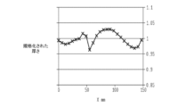
図4Bは、従来の面板を用いたCVDプロセスから生成された堆積層の直径の走査輪郭の一例を示している。図4Bでは、横軸が、面板の中心からの径方向の距離を表し、縦軸が、基板上の堆積層の、規格化された厚さを示している。従来の面板を用いた直径の走査輪郭は、堆積層の規格化された厚さが、基板の中央領域(約0mm~50mm)では、おおよそ0.87から0.95まで変動することを示している。 FIG. 4B shows an example of a scan profile of the diameter of a deposited layer produced from a CVD process using a conventional faceplate. In FIG. 4B, the horizontal axis represents the radial distance from the center of the faceplate, and the vertical axis represents the normalized thickness of the deposited layer on the substrate. Diameter scan profiles using a conventional face plate show that the normalized thickness of the deposited layer varies from approximately 0.87 to 0.95 in the central region of the substrate (approximately 0 mm to 50 mm). There is.
図4Cは、図4Aの面板200といった、本開示の面板を用いたCVDプロセスから生成された堆積層の直径の走査輪郭の一例を示している。面板から得られた直径の走査輪郭では、堆積層の規格化された厚さが、基板の中央領域内では、0.98から1まで変動することが示されている。
FIG. 4C shows an example of a scan profile of the diameter of a deposited layer produced from a CVD process using a faceplate of the present disclosure, such as
図4B及び図4Cの上記2つの走査輪郭を比較すると、面板の中央領域の放射率を調整することで、基板の中央領域内の膜堆積の厚さの変動が、0.13(1-0.87)から約0.02(1-0.98)に著しく減少しており、堆積層の均質性が約11%上がっていることが分かる。 Comparing the above two scan profiles in FIGS. 4B and 4C, it can be seen that by adjusting the emissivity of the central region of the faceplate, the variation in film deposition thickness within the central region of the substrate is 0.13 (1-0 .87) to about 0.02 (1-0.98), indicating that the homogeneity of the deposited layer has increased by about 11%.
先に示したように、面板の様々な領域の放射率が、基板及び/又は基板支持体の熱的な不均一性を補償して改善するために調整されうる。熱的な均一性が改善されることによって、対応して結果的に、堆積の均一性が改善されることになる。しかしながら、本明細書における態様は、面板の同心的な領域に関して説明しているが、放射率を変える様々な他のパターン又は構成が、面板の下面で利用されうると想定されることに注意されたい。 As indicated above, the emissivity of various regions of the faceplate can be adjusted to compensate for and improve thermal non-uniformities in the substrate and/or substrate support. Improved thermal uniformity results in a correspondingly improved deposition uniformity. However, it is noted that although aspects herein are described with respect to concentric regions of the faceplate, it is envisioned that various other patterns or configurations that vary emissivity may be utilized on the bottom surface of the faceplate. sea bream.
図5Aは、本開示の態様に係る、面板300の他の例を示している。面板300は、複数のガス分配孔301がそれを貫通して形成された本体302を含み、複数のガス分配孔301が、図3に示したように、ガス混合容積室102を主チャンバ処理容積室108へと流体的に接続する。本体302は、円筒形状で示されているが、矩形を含む他の形状も想定される。本体302は、石英、窒化ケイ素、アルミニウム、窒化アルミニウム、及び、ステンレス鋼といった1つ以上の物質から形成されうる。
FIG. 5A illustrates another example of a
一実施形態において、面板300は、第1の領域305、及び第2の領域310を含んでいる。面板300は、厚さプロファイルが様々な複数の領域を含んでおり、従って、その底面は非平面的である。例えば、第1の領域305の厚さと第2の領域310の厚さとの差は、約5%から45%の範囲内にありうる。第1の領域305は、第1の厚さを有する面板300の中央領域である。第2の領域310は、第1の領域305を取り囲む周辺領域であり、第1の厚さとは異なる第2の厚さを有する。
In one embodiment,
一実施形態において、第1の領域305の厚さは、第2の領域310の厚さよりも薄い。本実行形態では、第1の領域305は、第2の領域310に対して相対的に凹状とされている。上記凹部は、浅い円筒形状、又は、基板及び/又は基板支持体110に向かって反射される熱の調整を促進する他の適切な形状を含む様々な形状を有することが可能である。
In one embodiment, the thickness of the
面板300の様々な厚さによって、熱を分散させる代わりに、より長い期間の間面板300より下方で熱を保つ空間(例えば、凹部)が提供されうる。熱を保持することによって、互いに近隣に配置された基板の温度調整が促進され、従って、基板の温度の均一性の改善が可能となる。従って、厚さが様々な複数の領域を有する面板300によって、面板300の表面に形成された領域(例えば、凹部)の大きさ、位置、及び形状に従った、特定のエリアでの基板の温度の制御が可能となる。
The various thicknesses of the
一実施形態において、面板300は、その底面が、放射率が様々な複数の領域を含みうる。例えば、第1の領域305は、放射率がより高くなるよう表面が仕上げられた凹部を有することが可能であり、第2の領域310は、放射率がより低くなるよう表面が仕上げられてよい。本実施例では、非平面的な表面の特徴と、変更される放射率と、を組み合わせることによって、面板300が、基板の温度に対するより規模が大きな制御を提供する。
In one embodiment, the
図5Bは、従来の面板を用いたCVDプロセスから生成された堆積層の直径の走査輪郭の一例を示している。図5Bでは、横軸が、遮蔽板の中心からの径方向の距離を表し、縦軸が、基板上の堆積層の、規格化された厚さを示している。従来の遮蔽板を用いた直径の走査輪郭は、堆積層の規格化された厚さが、基板の中央領域(約0mm~50mm)では、おおよそ0.87から0.95まで変動することを示している。 FIG. 5B shows an example of a scan profile of the diameter of a deposited layer produced from a CVD process using a conventional faceplate. In FIG. 5B, the horizontal axis represents the radial distance from the center of the shield plate, and the vertical axis represents the normalized thickness of the deposited layer on the substrate. Diameter scan profiles using conventional shielding plates show that the normalized thickness of the deposited layer varies from approximately 0.87 to 0.95 in the central region of the substrate (approximately 0 mm to 50 mm). ing.
図5Cは、図5Aの面板300といった、本開示の面板を用いたCVDプロセスから生成された堆積層の例示的な直径の走査輪郭を示している。面板300から得られた直径の走査輪郭では、堆積層の規格化された厚さが、基板の中央領域では、0.97から1まで変動することが示されている。
FIG. 5C shows an exemplary diameter scan profile of a deposited layer produced from a CVD process using a faceplate of the present disclosure, such as
図5B及び図5Cの上記2つの走査輪郭を比較すると、面板300の中央領域305の放射率及び/又は相対的な位置を調整することで、基板の中央領域での膜堆積の厚さの変動が、0.13(1-0.87)から約0.03(1-0.97)に著しく減少しており、堆積層の均質性が約10%上がっていることが分かる。
Comparing the above two scan profiles of FIGS. 5B and 5C, it can be seen that by adjusting the emissivity and/or relative position of the
図6Aは、本開示の態様に係る遮蔽板400を示している。遮蔽板400は、図3に示す処理チャンバ100の遮蔽板104の代わりに使用されうる。
FIG. 6A shows a
本開示の態様に係る遮蔽板400は、流れプロファイルが様々な複数の領域を有する本体402を含んでいる。本体402は、円筒形状で示されているが、矩形を含む他の形状も想定される。本体402は、石英、窒化ケイ素、アルミニウム、窒化アルミニウム、及び、ステンレス鋼といった1つ以上の物質から形成されうる。一実施形態において、遮蔽板400は、第1の領域405及び第2の領域410を含む。第1の領域405は、第1の流れプロファイルを有する遮蔽板400の中央領域であり、第2の領域410は、第1の領域405を取り囲む周辺領域であり、第1の流れプロファイルとは異なる第2の流れプロファイルを有している。
A shielding
様々な流れプロファイルを獲得するために、遮蔽板400の各領域は、様々な密度及び様々な直径による、遮蔽板400を貫通して形成された孔を含みうる。一実施形態において、第1の領域405は、孔の密度がより高く、第2の領域410は、孔の密度がより低い。代替的に、第1の領域405は、孔の密度がより低くてよく、第2の領域410は、孔の密度がより高くてよい。他の実施形態において、第1の領域405が、直径がより大きい孔を有し、第2の領域410が、直径がより小さい孔を有している。代替的に、第1の領域405は、直径がより小さい孔を有してよく、第2の領域410は、直径がより大きい孔を有してよい。
To obtain different flow profiles, each region of the
概して、遮蔽板に設けられた密度がより高い孔又は直径がより大きい孔によって、より大きな流れプロファイルが生成され、遮蔽板に設けられた密度がより低い孔又は直径がより小さい孔によって、より小さな流れプロファイルが生成される。直径がより大きい孔又は密度がより高く配置された孔を通るガス流が増加すると、結果的に、前駆体材料の比較的より大きなガス流量を受け取る領域での、基板上の材料の堆積が増大することになる。従って、堆積の均一性が、ガス流量の調節を通じて改善されうる。同様に、遮蔽板の領域を通るガス流量が増大すると、結果的に、遮蔽板400(又はその近傍の面板)が局所的に冷却されることになり、堆積プロファイルの調整がさらに促進される。 In general, denser holes or larger diameter holes in the shield plate will produce a larger flow profile, and less dense or smaller diameter holes in the shield plate will produce a smaller flow profile. A flow profile is generated. Increased gas flow through larger diameter or more densely arranged pores results in increased deposition of material on the substrate in areas that receive a relatively greater gas flow rate of precursor material. I will do it. Accordingly, deposition uniformity can be improved through adjustment of gas flow rates. Similarly, increasing gas flow through the region of the shield plate results in localized cooling of the shield plate 400 (or the face plate in its vicinity), further facilitating deposition profile tailoring.
遮蔽板400は、孔の大きさ/密度が異なる領域に加えて、放射率が異なる又は相対的厚さが様々な複数の領域も含みうることが想定される。従って、温度及び堆積の均一性が、遮蔽板の表面に亘る複数の変更を通じてさらに調整されうる。
It is envisioned that the shielding
流れプロファイルが様々な複数の領域を含む遮蔽板400によって、各領域内に形成された孔の数、大きさ、及び位置に従った、基板の温度の制御が可能となる。その結果、基板の温度が制御されることによって、基板の表面の堆積の均一性が改善される。
A shielding
図6Bは、2つの例示的な直径の走査輪郭を示しており、一方は、従来の(即ち、旧型の)遮蔽板についての堆積層の直径の走査輪郭であり、他方は、図6Aに示した遮蔽板400といった、本開示に係る遮蔽板の直径の走査輪郭である。2つの直径の走査輪郭の比較によって、選択された領域内での遮蔽板の表面に亘る遮蔽板の流れプロファイルを調整することによって、中央領域と周辺領域との間で膜堆積の厚さを調整することが可能であることが示されている。
FIG. 6B shows two exemplary diameter scan profiles, one for a conventional (i.e., old-style) shield, and the other for a conventional (i.e., old-style) shield, and the other as shown in FIG. 6A. 4 is a scanned profile of the diameter of a shielding plate according to the present disclosure, such as shielding
図7は、本開示の実施形態に係る遮蔽部500を示している。放射遮蔽体500は、本体502を含んでおり、本体502には、直径が同じ又は異なる複数の孔501が貫通して形成されている。本体502は、円筒形状で示されているが、矩形を含む他の形状も想定される。本体502は、石英、窒化ケイ素、アルミニウム、窒化アルミニウム、及び、ステンレス鋼といった1つ以上の物質から形成されうる。複数の孔501が、共通軸の周囲に環状に配置されうる。各環状パターンにおける孔501の密度及び孔501の直径は、様々でありうる。結果的に、隣り合う孔501の間の間隔が様々であり、孔501の流れプロファイルが、孔501の位置及び大きさに従って様々である。
FIG. 7 shows a
一実施形態において、複数の孔501が、共通の中心を有する3つの環状パターン505、510、及び515で配置されている。環状パターン505及び515の孔501の密度は、環状パターン510の孔501の密度よりも高い。しかしながら、本開示の範囲はこれには限定されず、環状パターン505、510、又は515のいずれも、他の環状パターン505、510、及び515よりも密度が高い孔を有しうる。幾つかの実施形態において、環状パターン510の孔501の直径は、環状パターン505及び515の孔501の直径よりも大きい。代替的に、いずれの環状パターン505、510、又は515の孔501の直径も、他の環状パターン505、510、及び515の孔501の直径よりも大きくてよい。
In one embodiment, the plurality of
放射遮蔽体500は、孔501の大きさ、位置、及び数に従って、様々なパターンによる孔501を有しうる。放射遮蔽体500は、基板支持体110の底面の下方に配置されうる。従って、放射遮蔽体500に様々なパターンの孔501を作ることによって、基板支持体110の底面での放射熱の損失を調節することが可能であり、基板支持体110のいかなる温度の不均一性も補償され、従って、基板支持体110に載置された基板の不均一性が補償される。
The
他の実施形態において、シャフト114は、例えば基板支持体110の底部の近傍のシャフト114の上端に、(図1に示した)複数の孔115を有する。熱伝導性のガス又は混合ガス、即ち例えば、He/H2又はArが、基板支持体110のシャフトに設けられた複数の孔から、主処理チャンバ容積室108の中へと流れうる。幾つかの実施形態において、熱伝導性のガスが、外部のガス源(図示せず)から、シャフトの内部管を通じて供給される。流量が様々であり混合ガスが様々であると、基板支持体110と底部の熱伝導性ガスとの間の対流熱損失が、径方向における基板支持体110の温度プロファイルを調節することが可能である。
In other embodiments, the
先に記載した実施形態を、面板及び遮蔽板の特性を局所的に調整することによって薄膜の堆積の均一性を改善するために、個別に又は組み合わせて利用することが可能である。さらに、本明細書の実施形態は、概して、放射率、相対的位置、又は流量密度が変更される2つの領域によって記載されたが、本明細書に記載の面板及び遮蔽板は、2つの各領域より多くの領域を含みうることが想定される。2つより多くの領域を含むことによって、均一性及び/又は同調性がさらに改善される。 The embodiments described above can be utilized individually or in combination to improve the uniformity of thin film deposition by locally adjusting the properties of the face plate and the shield plate. Additionally, while the embodiments herein have been generally described with two regions in which emissivity, relative position, or flow density is changed, the face plate and shield plate described herein have two regions in each region. It is envisioned that it may contain more than one region. Including more than two regions further improves uniformity and/or synchronization.
以上の説明は本開示の態様を対象としているが、本開示の基本的な範囲を逸脱しなければ、本開示の他の態様及び更なる態様が考案されてよく、本開示の範囲は以下の特許請求の範囲によって決まる。 Although the above description is directed to aspects of the disclosure, other and further aspects of the disclosure may be devised without departing from the essential scope of the disclosure, and the scope of the disclosure includes the following: Depends on the scope of the claims.
Claims (8)
処理容積室を内側に画定するチャンバ本体及びチャンバリッドと、
前記処理容積室内に配置された基板支持体と、
前記処理容積室内において前記基板支持体と対向して配置された遮蔽板であって、前記遮蔽板にはそれを貫通する複数の孔が形成されている、遮蔽板と、
複数の孔がそれを貫通して形成された面板であって、前記面板は、前記処理容積室において前記遮蔽板と前記基板支持体との間に配置され、前記面板は、前記面板と前記遮蔽板との間に容積室を少なくとも部分的に画定し、前記面板は、第1の表面領域と、前記第1の表面領域を取り囲む第2の表面領域と、を有し、前記第1の表面領域は、前記第2の表面領域に対して相対的に凹状とされている、面板と
を含む、基板に膜を堆積させるための装置。 An apparatus for depositing a film on a substrate, the apparatus comprising:
a chamber body and a chamber lid defining a processing volume chamber therein;
a substrate support disposed within the processing volume;
a shielding plate disposed opposite the substrate support in the processing volume chamber, the shielding plate having a plurality of holes formed therethrough;
a face plate having a plurality of holes formed therethrough, the face plate being disposed between the shielding plate and the substrate support in the processing volume chamber, the face plate having a plurality of holes formed therethrough; at least partially defining a volume between the faceplate and the faceplate, the faceplate having a first surface area and a second surface area surrounding the first surface area; a face plate, the region being concave relative to the second surface region.
前記第1の表面領域を貫通して形成された第1の複数のガス分配孔であって、前記第1の複数のガス分配孔は第1の密度を有し、前記第1の複数のガス分配孔の各々は第1の直径を有する、第1の複数のガス分配孔と、
前記第2の表面領域を貫通して形成された第2の複数のガス分配孔であって、前記第2の複数のガス分配孔は第2の密度を有し、前記第2の密度は前記第1の密度とは異なり、前記第2の複数のガス分配孔の各々は第2の直径を有し、前記第2の直径は前記第1の直径とは異なる、第2の複数のガス分配孔と
をさらに含む、請求項1に記載の装置。 The shielding plate is
a first plurality of gas distribution holes formed through the first surface region, the first plurality of gas distribution holes having a first density; a first plurality of gas distribution holes, each distribution hole having a first diameter;
a second plurality of gas distribution holes formed through the second surface region, the second plurality of gas distribution holes having a second density; a second plurality of gas distribution holes, each of the second plurality of gas distribution holes having a second diameter, the second diameter being different from the first diameter; 2. The device of claim 1 , further comprising: a hole.
Priority Applications (1)
| Application Number | Priority Date | Filing Date | Title |
|---|---|---|---|
| JP2023130632A JP2023175682A (en) | 2017-08-11 | 2023-08-10 | Apparatus and methods for improving thermal chemical vapor deposition (cvd) uniformity |
Applications Claiming Priority (3)
| Application Number | Priority Date | Filing Date | Title |
|---|---|---|---|
| US201762544507P | 2017-08-11 | 2017-08-11 | |
| US62/544,507 | 2017-08-11 | ||
| PCT/US2018/046344 WO2019033052A1 (en) | 2017-08-11 | 2018-08-10 | Apparatus and methods for improving thermal chemical vapor deposition (cvd) uniformity |
Related Child Applications (1)
| Application Number | Title | Priority Date | Filing Date |
|---|---|---|---|
| JP2023130632A Division JP2023175682A (en) | 2017-08-11 | 2023-08-10 | Apparatus and methods for improving thermal chemical vapor deposition (cvd) uniformity |
Publications (3)
| Publication Number | Publication Date |
|---|---|
| JP2020530527A JP2020530527A (en) | 2020-10-22 |
| JP2020530527A5 JP2020530527A5 (en) | 2021-09-16 |
| JP7384784B2 true JP7384784B2 (en) | 2023-11-21 |
Family
ID=65271311
Family Applications (2)
| Application Number | Title | Priority Date | Filing Date |
|---|---|---|---|
| JP2020506157A Active JP7384784B2 (en) | 2017-08-11 | 2018-08-10 | Apparatus and method for improving uniformity in thermal chemical vapor deposition (CVD) |
| JP2023130632A Pending JP2023175682A (en) | 2017-08-11 | 2023-08-10 | Apparatus and methods for improving thermal chemical vapor deposition (cvd) uniformity |
Family Applications After (1)
| Application Number | Title | Priority Date | Filing Date |
|---|---|---|---|
| JP2023130632A Pending JP2023175682A (en) | 2017-08-11 | 2023-08-10 | Apparatus and methods for improving thermal chemical vapor deposition (cvd) uniformity |
Country Status (5)
| Country | Link |
|---|---|
| US (1) | US11939675B2 (en) |
| JP (2) | JP7384784B2 (en) |
| KR (1) | KR20200030591A (en) |
| CN (1) | CN111066133B (en) |
| WO (1) | WO2019033052A1 (en) |
Families Citing this family (6)
| Publication number | Priority date | Publication date | Assignee | Title |
|---|---|---|---|---|
| KR102560283B1 (en) * | 2018-01-24 | 2023-07-26 | 삼성전자주식회사 | Apparatus and method for manufacturing and designing a shower head |
| JP2022535285A (en) | 2019-06-07 | 2022-08-05 | アプライド マテリアルズ インコーポレイテッド | Face plate with curved surface |
| US11600470B2 (en) | 2019-12-27 | 2023-03-07 | Applied Materials, Inc. | Targeted heat control systems |
| TW202147492A (en) * | 2020-06-03 | 2021-12-16 | 荷蘭商Asm Ip私人控股有限公司 | Shower plate, substrate treatment device, and substate treatment method |
| US11946140B2 (en) * | 2021-03-26 | 2024-04-02 | Applied Materials, Inc. | Hot showerhead |
| CN115125520B (en) * | 2022-08-09 | 2023-11-24 | 季华恒一(佛山)半导体科技有限公司 | Even gas board and coating device |
Citations (8)
| Publication number | Priority date | Publication date | Assignee | Title |
|---|---|---|---|---|
| JP2002299240A (en) | 2001-03-28 | 2002-10-11 | Tadahiro Omi | Plasma processor |
| US20120108066A1 (en) | 2010-10-28 | 2012-05-03 | Texas Instruments Incorporated | Pecvd showerhead configuration for cmp uniformity and improved stress |
| JP2012142329A (en) | 2010-12-28 | 2012-07-26 | Toshiba Corp | Processing equipment |
| US20130164948A1 (en) | 2011-12-22 | 2013-06-27 | Intermolecular, Inc. | Methods for improving wafer temperature uniformity |
| US20130334344A1 (en) | 2012-06-15 | 2013-12-19 | Karl F. Leeser | Contoured showerhead for improved plasma shaping and control |
| JP2015529395A (en) | 2012-08-23 | 2015-10-05 | アプライド マテリアルズ インコーポレイテッドApplied Materials,Incorporated | Method and hardware for cleaning a UV chamber |
| US20160099147A1 (en) | 2014-10-03 | 2016-04-07 | Applied Materials, Inc. | Gas flow profile modulated control of overlay in plasma cvd films |
| JP2017112371A (en) | 2015-12-14 | 2017-06-22 | ラム リサーチ コーポレーションLam Research Corporation | Showerhead assembly |
Family Cites Families (20)
| Publication number | Priority date | Publication date | Assignee | Title |
|---|---|---|---|---|
| DE2610556C2 (en) * | 1976-03-12 | 1978-02-02 | Siemens AG, 1000 Berlin und 8000 München | Device for distributing flowing media over a flow cross-section |
| US5133284A (en) * | 1990-07-16 | 1992-07-28 | National Semiconductor Corp. | Gas-based backside protection during substrate processing |
| JP3824675B2 (en) | 1995-03-03 | 2006-09-20 | 有限会社デジタル・ウェーブ | Crystal manufacturing equipment |
| US6301434B1 (en) * | 1998-03-23 | 2001-10-09 | Mattson Technology, Inc. | Apparatus and method for CVD and thermal processing of semiconductor substrates |
| JPH11279778A (en) * | 1998-03-30 | 1999-10-12 | Seiko Epson Corp | Etching apparatus and production of semiconductor device |
| US6245192B1 (en) | 1999-06-30 | 2001-06-12 | Lam Research Corporation | Gas distribution apparatus for semiconductor processing |
| JP2007042951A (en) | 2005-08-04 | 2007-02-15 | Tokyo Electron Ltd | Plasma processing device |
| TW200711029A (en) * | 2005-08-05 | 2007-03-16 | Tokyo Electron Ltd | Substrate processing apparatus and substrate stage used therein |
| US8142606B2 (en) | 2007-06-07 | 2012-03-27 | Applied Materials, Inc. | Apparatus for depositing a uniform silicon film and methods for manufacturing the same |
| US8291857B2 (en) * | 2008-07-03 | 2012-10-23 | Applied Materials, Inc. | Apparatuses and methods for atomic layer deposition |
| JP5487049B2 (en) | 2010-08-19 | 2014-05-07 | 株式会社日本マイクロニクス | Probe card |
| KR101232200B1 (en) * | 2010-12-28 | 2013-02-12 | 피에스케이 주식회사 | Baffle, apparatus for treating substrate and method for treating thereof |
| JP5550602B2 (en) * | 2011-04-28 | 2014-07-16 | パナソニック株式会社 | Electrostatic chuck and dry etching apparatus having the same |
| US9167625B2 (en) | 2011-11-23 | 2015-10-20 | Asm Ip Holding B.V. | Radiation shielding for a substrate holder |
| KR20130111029A (en) * | 2012-03-30 | 2013-10-10 | 삼성전자주식회사 | Susceptor for chemical vapor deposition apparatus and chemical vapor deposition apparatus having the same |
| US20130284092A1 (en) * | 2012-04-25 | 2013-10-31 | Applied Materials, Inc. | Faceplate having regions of differing emissivity |
| KR20150049180A (en) | 2013-10-29 | 2015-05-08 | 세메스 주식회사 | Apparatus for Processing Substrate |
| JP5726281B1 (en) | 2013-12-27 | 2015-05-27 | 株式会社日立国際電気 | Substrate processing apparatus and semiconductor device manufacturing method |
| KR20170048578A (en) * | 2014-09-05 | 2017-05-08 | 어플라이드 머티어리얼스, 인코포레이티드 | Atmospheric epitaxial deposition chamber |
| KR102528559B1 (en) * | 2016-07-26 | 2023-05-04 | 삼성전자주식회사 | Apparatus for manufacturing a large size substrate |
-
2018
- 2018-08-10 CN CN201880056745.6A patent/CN111066133B/en active Active
- 2018-08-10 KR KR1020207005044A patent/KR20200030591A/en not_active Application Discontinuation
- 2018-08-10 WO PCT/US2018/046344 patent/WO2019033052A1/en active Application Filing
- 2018-08-10 US US16/636,659 patent/US11939675B2/en active Active
- 2018-08-10 JP JP2020506157A patent/JP7384784B2/en active Active
-
2023
- 2023-08-10 JP JP2023130632A patent/JP2023175682A/en active Pending
Patent Citations (8)
| Publication number | Priority date | Publication date | Assignee | Title |
|---|---|---|---|---|
| JP2002299240A (en) | 2001-03-28 | 2002-10-11 | Tadahiro Omi | Plasma processor |
| US20120108066A1 (en) | 2010-10-28 | 2012-05-03 | Texas Instruments Incorporated | Pecvd showerhead configuration for cmp uniformity and improved stress |
| JP2012142329A (en) | 2010-12-28 | 2012-07-26 | Toshiba Corp | Processing equipment |
| US20130164948A1 (en) | 2011-12-22 | 2013-06-27 | Intermolecular, Inc. | Methods for improving wafer temperature uniformity |
| US20130334344A1 (en) | 2012-06-15 | 2013-12-19 | Karl F. Leeser | Contoured showerhead for improved plasma shaping and control |
| JP2015529395A (en) | 2012-08-23 | 2015-10-05 | アプライド マテリアルズ インコーポレイテッドApplied Materials,Incorporated | Method and hardware for cleaning a UV chamber |
| US20160099147A1 (en) | 2014-10-03 | 2016-04-07 | Applied Materials, Inc. | Gas flow profile modulated control of overlay in plasma cvd films |
| JP2017112371A (en) | 2015-12-14 | 2017-06-22 | ラム リサーチ コーポレーションLam Research Corporation | Showerhead assembly |
Also Published As
| Publication number | Publication date |
|---|---|
| CN111066133A (en) | 2020-04-24 |
| JP2020530527A (en) | 2020-10-22 |
| JP2023175682A (en) | 2023-12-12 |
| CN111066133B (en) | 2023-08-22 |
| KR20200030591A (en) | 2020-03-20 |
| US11939675B2 (en) | 2024-03-26 |
| WO2019033052A1 (en) | 2019-02-14 |
| US20210147981A1 (en) | 2021-05-20 |
Similar Documents
| Publication | Publication Date | Title |
|---|---|---|
| JP7384784B2 (en) | Apparatus and method for improving uniformity in thermal chemical vapor deposition (CVD) | |
| US20200241580A1 (en) | Multi-channel flow ratio controller and processing chamber | |
| EP3275008B1 (en) | Chamber components for epitaxial growth apparatus | |
| TW201944523A (en) | Substrate supporting apparatus, substrate processing apparatus including the same, and substrate processing method | |
| US20090095221A1 (en) | Multi-gas concentric injection showerhead | |
| US20160068996A1 (en) | Susceptor and pre-heat ring for thermal processing of substrates | |
| US11807931B2 (en) | Chamber injector | |
| JP7401560B2 (en) | Heat treatment chamber lid with backside pumping | |
| JP2022544221A (en) | Spatial adjustment deposition to compensate for various bows in the wafer | |
| US20190048467A1 (en) | Showerhead and process chamber incorporating same | |
| US20230044440A1 (en) | Film forming apparatus and plate | |
| US20230243065A1 (en) | Methods for manufacturing a semiconductor wafer using a preheat ring in a wafer reactor | |
| TWI754765B (en) | Inject assembly for epitaxial deposition processes | |
| CN109487237B (en) | Apparatus and method for chemical vapor deposition process for semiconductor substrate | |
| TW202031925A (en) | Method for setting up or operating a CVD reactor | |
| TWI666350B (en) | Liner for epi chamber | |
| US5044315A (en) | Apparatus for improving the reactant gas flow in a reaction chamber | |
| US20240110278A1 (en) | Dog bone exhaust slit tunnel for processing chambers | |
| KR102337411B1 (en) | Deposition apparatus |
Legal Events
| Date | Code | Title | Description |
|---|---|---|---|
| A521 | Request for written amendment filed |
Free format text: JAPANESE INTERMEDIATE CODE: A523 Effective date: 20210803 |
|
| A621 | Written request for application examination |
Free format text: JAPANESE INTERMEDIATE CODE: A621 Effective date: 20210803 |
|
| A977 | Report on retrieval |
Free format text: JAPANESE INTERMEDIATE CODE: A971007 Effective date: 20220725 |
|
| A131 | Notification of reasons for refusal |
Free format text: JAPANESE INTERMEDIATE CODE: A131 Effective date: 20220906 |
|
| A02 | Decision of refusal |
Free format text: JAPANESE INTERMEDIATE CODE: A02 Effective date: 20230411 |
|
| A521 | Request for written amendment filed |
Free format text: JAPANESE INTERMEDIATE CODE: A523 Effective date: 20230810 |
|
| A911 | Transfer to examiner for re-examination before appeal (zenchi) |
Free format text: JAPANESE INTERMEDIATE CODE: A911 Effective date: 20230818 |
|
| TRDD | Decision of grant or rejection written | ||
| A01 | Written decision to grant a patent or to grant a registration (utility model) |
Free format text: JAPANESE INTERMEDIATE CODE: A01 Effective date: 20231024 |
|
| A61 | First payment of annual fees (during grant procedure) |
Free format text: JAPANESE INTERMEDIATE CODE: A61 Effective date: 20231109 |
|
| R150 | Certificate of patent or registration of utility model |
Ref document number: 7384784 Country of ref document: JP Free format text: JAPANESE INTERMEDIATE CODE: R150 |