JP7380720B2 - Semiconductor device, pH sensor, biosensor, and method for manufacturing semiconductor device - Google Patents
Semiconductor device, pH sensor, biosensor, and method for manufacturing semiconductor device Download PDFInfo
- Publication number
- JP7380720B2 JP7380720B2 JP2022003648A JP2022003648A JP7380720B2 JP 7380720 B2 JP7380720 B2 JP 7380720B2 JP 2022003648 A JP2022003648 A JP 2022003648A JP 2022003648 A JP2022003648 A JP 2022003648A JP 7380720 B2 JP7380720 B2 JP 7380720B2
- Authority
- JP
- Japan
- Prior art keywords
- manufacturing
- semiconductor layer
- electrode
- layer
- forming
- Prior art date
- Legal status (The legal status is an assumption and is not a legal conclusion. Google has not performed a legal analysis and makes no representation as to the accuracy of the status listed.)
- Active
Links
- 239000004065 semiconductor Substances 0.000 title claims description 112
- 238000000034 method Methods 0.000 title claims description 54
- 238000004519 manufacturing process Methods 0.000 title claims description 41
- 238000005530 etching Methods 0.000 claims description 19
- 238000004544 sputter deposition Methods 0.000 claims description 12
- 239000003929 acidic solution Substances 0.000 claims description 8
- UFHFLCQGNIYNRP-UHFFFAOYSA-N Hydrogen Chemical compound [H][H] UFHFLCQGNIYNRP-UHFFFAOYSA-N 0.000 claims description 7
- 239000001257 hydrogen Substances 0.000 claims description 7
- 229910052739 hydrogen Inorganic materials 0.000 claims description 7
- 229910052596 spinel Inorganic materials 0.000 claims description 4
- 239000011029 spinel Substances 0.000 claims description 4
- 239000010410 layer Substances 0.000 description 77
- 239000000243 solution Substances 0.000 description 19
- 239000010408 film Substances 0.000 description 18
- XLOMVQKBTHCTTD-UHFFFAOYSA-N Zinc monoxide Chemical compound [Zn]=O XLOMVQKBTHCTTD-UHFFFAOYSA-N 0.000 description 16
- 239000000463 material Substances 0.000 description 16
- 238000005259 measurement Methods 0.000 description 14
- 239000002253 acid Substances 0.000 description 13
- 239000000758 substrate Substances 0.000 description 13
- 239000002585 base Substances 0.000 description 10
- 229910052733 gallium Inorganic materials 0.000 description 10
- 230000008569 process Effects 0.000 description 10
- 239000010409 thin film Substances 0.000 description 9
- 150000007513 acids Chemical class 0.000 description 8
- 238000002161 passivation Methods 0.000 description 8
- 239000011241 protective layer Substances 0.000 description 8
- 239000011701 zinc Substances 0.000 description 8
- 239000011787 zinc oxide Substances 0.000 description 8
- GYHNNYVSQQEPJS-UHFFFAOYSA-N Gallium Chemical compound [Ga] GYHNNYVSQQEPJS-UHFFFAOYSA-N 0.000 description 7
- 238000002474 experimental method Methods 0.000 description 7
- 239000000126 substance Substances 0.000 description 6
- 230000015572 biosynthetic process Effects 0.000 description 5
- 239000007789 gas Substances 0.000 description 5
- 229910052751 metal Inorganic materials 0.000 description 5
- 239000002184 metal Substances 0.000 description 5
- 239000000203 mixture Substances 0.000 description 5
- 229910052725 zinc Inorganic materials 0.000 description 5
- VEXZGXHMUGYJMC-UHFFFAOYSA-N Hydrochloric acid Chemical compound Cl VEXZGXHMUGYJMC-UHFFFAOYSA-N 0.000 description 4
- XUIMIQQOPSSXEZ-UHFFFAOYSA-N Silicon Chemical compound [Si] XUIMIQQOPSSXEZ-UHFFFAOYSA-N 0.000 description 4
- 238000002441 X-ray diffraction Methods 0.000 description 4
- 229910052782 aluminium Inorganic materials 0.000 description 4
- 229910052710 silicon Inorganic materials 0.000 description 4
- 239000010703 silicon Substances 0.000 description 4
- 229910000838 Al alloy Inorganic materials 0.000 description 3
- 229910021364 Al-Si alloy Inorganic materials 0.000 description 3
- 229910001096 P alloy Inorganic materials 0.000 description 3
- HEMHJVSKTPXQMS-UHFFFAOYSA-M Sodium hydroxide Chemical compound [OH-].[Na+] HEMHJVSKTPXQMS-UHFFFAOYSA-M 0.000 description 3
- 229910001080 W alloy Inorganic materials 0.000 description 3
- 230000002378 acidificating effect Effects 0.000 description 3
- 230000000052 comparative effect Effects 0.000 description 3
- 229910052802 copper Inorganic materials 0.000 description 3
- 238000001514 detection method Methods 0.000 description 3
- 238000010586 diagram Methods 0.000 description 3
- 150000002739 metals Chemical class 0.000 description 3
- 229910052750 molybdenum Inorganic materials 0.000 description 3
- 239000002356 single layer Substances 0.000 description 3
- JBQYATWDVHIOAR-UHFFFAOYSA-N tellanylidenegermanium Chemical compound [Te]=[Ge] JBQYATWDVHIOAR-UHFFFAOYSA-N 0.000 description 3
- 229910052721 tungsten Inorganic materials 0.000 description 3
- 229910018072 Al 2 O 3 Inorganic materials 0.000 description 2
- 229910005191 Ga 2 O 3 Inorganic materials 0.000 description 2
- -1 Si 3 N 4 Inorganic materials 0.000 description 2
- 229910004298 SiO 2 Inorganic materials 0.000 description 2
- HCHKCACWOHOZIP-UHFFFAOYSA-N Zinc Chemical compound [Zn] HCHKCACWOHOZIP-UHFFFAOYSA-N 0.000 description 2
- QVGXLLKOCUKJST-UHFFFAOYSA-N atomic oxygen Chemical compound [O] QVGXLLKOCUKJST-UHFFFAOYSA-N 0.000 description 2
- 230000008901 benefit Effects 0.000 description 2
- 230000008859 change Effects 0.000 description 2
- AJNVQOSZGJRYEI-UHFFFAOYSA-N digallium;oxygen(2-) Chemical compound [O-2].[O-2].[O-2].[Ga+3].[Ga+3] AJNVQOSZGJRYEI-UHFFFAOYSA-N 0.000 description 2
- 229910001195 gallium oxide Inorganic materials 0.000 description 2
- 238000010438 heat treatment Methods 0.000 description 2
- 229910052738 indium Inorganic materials 0.000 description 2
- 150000002500 ions Chemical class 0.000 description 2
- 230000001590 oxidative effect Effects 0.000 description 2
- 239000001301 oxygen Substances 0.000 description 2
- 229910052760 oxygen Inorganic materials 0.000 description 2
- 238000000206 photolithography Methods 0.000 description 2
- 238000011282 treatment Methods 0.000 description 2
- XLYOFNOQVPJJNP-UHFFFAOYSA-N water Substances O XLYOFNOQVPJJNP-UHFFFAOYSA-N 0.000 description 2
- YCKRFDGAMUMZLT-UHFFFAOYSA-N Fluorine atom Chemical compound [F] YCKRFDGAMUMZLT-UHFFFAOYSA-N 0.000 description 1
- 229910021607 Silver chloride Inorganic materials 0.000 description 1
- 229910007541 Zn O Inorganic materials 0.000 description 1
- 239000012670 alkaline solution Substances 0.000 description 1
- 229910045601 alloy Inorganic materials 0.000 description 1
- 239000000956 alloy Substances 0.000 description 1
- 229910052787 antimony Inorganic materials 0.000 description 1
- 239000003637 basic solution Substances 0.000 description 1
- GTKRFUAGOKINCA-UHFFFAOYSA-M chlorosilver;silver Chemical compound [Ag].[Ag]Cl GTKRFUAGOKINCA-UHFFFAOYSA-M 0.000 description 1
- 239000013078 crystal Substances 0.000 description 1
- 238000007599 discharging Methods 0.000 description 1
- 238000001312 dry etching Methods 0.000 description 1
- 230000003628 erosive effect Effects 0.000 description 1
- 230000008020 evaporation Effects 0.000 description 1
- 238000001704 evaporation Methods 0.000 description 1
- 230000005669 field effect Effects 0.000 description 1
- 229910052731 fluorine Inorganic materials 0.000 description 1
- 239000011737 fluorine Substances 0.000 description 1
- 239000011888 foil Substances 0.000 description 1
- 239000011521 glass Substances 0.000 description 1
- 230000007246 mechanism Effects 0.000 description 1
- 229910021645 metal ion Inorganic materials 0.000 description 1
- 238000001139 pH measurement Methods 0.000 description 1
- 239000002245 particle Substances 0.000 description 1
- 238000003672 processing method Methods 0.000 description 1
- 238000006479 redox reaction Methods 0.000 description 1
- 230000004044 response Effects 0.000 description 1
- 230000035945 sensitivity Effects 0.000 description 1
- 229910052814 silicon oxide Inorganic materials 0.000 description 1
- 229920002379 silicone rubber Polymers 0.000 description 1
- HKZLPVFGJNLROG-UHFFFAOYSA-M silver monochloride Chemical compound [Cl-].[Ag+] HKZLPVFGJNLROG-UHFFFAOYSA-M 0.000 description 1
- 229910052715 tantalum Inorganic materials 0.000 description 1
- 229910052718 tin Inorganic materials 0.000 description 1
- 238000001039 wet etching Methods 0.000 description 1
Images


Classifications
-
- H—ELECTRICITY
- H01—ELECTRIC ELEMENTS
- H01L—SEMICONDUCTOR DEVICES NOT COVERED BY CLASS H10
- H01L21/00—Processes or apparatus adapted for the manufacture or treatment of semiconductor or solid state devices or of parts thereof
- H01L21/02—Manufacture or treatment of semiconductor devices or of parts thereof
- H01L21/02104—Forming layers
- H01L21/02365—Forming inorganic semiconducting materials on a substrate
- H01L21/02518—Deposited layers
- H01L21/02521—Materials
- H01L21/02551—Group 12/16 materials
- H01L21/02554—Oxides
-
- H—ELECTRICITY
- H01—ELECTRIC ELEMENTS
- H01L—SEMICONDUCTOR DEVICES NOT COVERED BY CLASS H10
- H01L29/00—Semiconductor devices adapted for rectifying, amplifying, oscillating or switching, or capacitors or resistors with at least one potential-jump barrier or surface barrier, e.g. PN junction depletion layer or carrier concentration layer; Details of semiconductor bodies or of electrodes thereof ; Multistep manufacturing processes therefor
- H01L29/66—Types of semiconductor device ; Multistep manufacturing processes therefor
- H01L29/68—Types of semiconductor device ; Multistep manufacturing processes therefor controllable by only the electric current supplied, or only the electric potential applied, to an electrode which does not carry the current to be rectified, amplified or switched
- H01L29/76—Unipolar devices, e.g. field effect transistors
- H01L29/772—Field effect transistors
- H01L29/78—Field effect transistors with field effect produced by an insulated gate
- H01L29/786—Thin film transistors, i.e. transistors with a channel being at least partly a thin film
- H01L29/7869—Thin film transistors, i.e. transistors with a channel being at least partly a thin film having a semiconductor body comprising an oxide semiconductor material, e.g. zinc oxide, copper aluminium oxide, cadmium stannate
-
- G—PHYSICS
- G01—MEASURING; TESTING
- G01N—INVESTIGATING OR ANALYSING MATERIALS BY DETERMINING THEIR CHEMICAL OR PHYSICAL PROPERTIES
- G01N27/00—Investigating or analysing materials by the use of electric, electrochemical, or magnetic means
- G01N27/26—Investigating or analysing materials by the use of electric, electrochemical, or magnetic means by investigating electrochemical variables; by using electrolysis or electrophoresis
- G01N27/403—Cells and electrode assemblies
- G01N27/414—Ion-sensitive or chemical field-effect transistors, i.e. ISFETS or CHEMFETS
- G01N27/4145—Ion-sensitive or chemical field-effect transistors, i.e. ISFETS or CHEMFETS specially adapted for biomolecules, e.g. gate electrode with immobilised receptors
-
- H—ELECTRICITY
- H01—ELECTRIC ELEMENTS
- H01L—SEMICONDUCTOR DEVICES NOT COVERED BY CLASS H10
- H01L21/00—Processes or apparatus adapted for the manufacture or treatment of semiconductor or solid state devices or of parts thereof
- H01L21/02—Manufacture or treatment of semiconductor devices or of parts thereof
- H01L21/02104—Forming layers
- H01L21/02365—Forming inorganic semiconducting materials on a substrate
- H01L21/02367—Substrates
- H01L21/0237—Materials
- H01L21/02373—Group 14 semiconducting materials
- H01L21/02381—Silicon, silicon germanium, germanium
-
- H—ELECTRICITY
- H01—ELECTRIC ELEMENTS
- H01L—SEMICONDUCTOR DEVICES NOT COVERED BY CLASS H10
- H01L21/00—Processes or apparatus adapted for the manufacture or treatment of semiconductor or solid state devices or of parts thereof
- H01L21/02—Manufacture or treatment of semiconductor devices or of parts thereof
- H01L21/02104—Forming layers
- H01L21/02365—Forming inorganic semiconducting materials on a substrate
- H01L21/02436—Intermediate layers between substrates and deposited layers
- H01L21/02439—Materials
- H01L21/02488—Insulating materials
-
- H—ELECTRICITY
- H01—ELECTRIC ELEMENTS
- H01L—SEMICONDUCTOR DEVICES NOT COVERED BY CLASS H10
- H01L21/00—Processes or apparatus adapted for the manufacture or treatment of semiconductor or solid state devices or of parts thereof
- H01L21/02—Manufacture or treatment of semiconductor devices or of parts thereof
- H01L21/02104—Forming layers
- H01L21/02365—Forming inorganic semiconducting materials on a substrate
- H01L21/02518—Deposited layers
- H01L21/02521—Materials
- H01L21/02565—Oxide semiconducting materials not being Group 12/16 materials, e.g. ternary compounds
-
- H—ELECTRICITY
- H01—ELECTRIC ELEMENTS
- H01L—SEMICONDUCTOR DEVICES NOT COVERED BY CLASS H10
- H01L21/00—Processes or apparatus adapted for the manufacture or treatment of semiconductor or solid state devices or of parts thereof
- H01L21/02—Manufacture or treatment of semiconductor devices or of parts thereof
- H01L21/02104—Forming layers
- H01L21/02365—Forming inorganic semiconducting materials on a substrate
- H01L21/02518—Deposited layers
- H01L21/0257—Doping during depositing
- H01L21/02573—Conductivity type
- H01L21/02576—N-type
-
- H—ELECTRICITY
- H01—ELECTRIC ELEMENTS
- H01L—SEMICONDUCTOR DEVICES NOT COVERED BY CLASS H10
- H01L21/00—Processes or apparatus adapted for the manufacture or treatment of semiconductor or solid state devices or of parts thereof
- H01L21/02—Manufacture or treatment of semiconductor devices or of parts thereof
- H01L21/04—Manufacture or treatment of semiconductor devices or of parts thereof the devices having at least one potential-jump barrier or surface barrier, e.g. PN junction, depletion layer or carrier concentration layer
- H01L21/18—Manufacture or treatment of semiconductor devices or of parts thereof the devices having at least one potential-jump barrier or surface barrier, e.g. PN junction, depletion layer or carrier concentration layer the devices having semiconductor bodies comprising elements of Group IV of the Periodic System or AIIIBV compounds with or without impurities, e.g. doping materials
- H01L21/30—Treatment of semiconductor bodies using processes or apparatus not provided for in groups H01L21/20 - H01L21/26
- H01L21/302—Treatment of semiconductor bodies using processes or apparatus not provided for in groups H01L21/20 - H01L21/26 to change their surface-physical characteristics or shape, e.g. etching, polishing, cutting
- H01L21/306—Chemical or electrical treatment, e.g. electrolytic etching
- H01L21/30604—Chemical etching
-
- H—ELECTRICITY
- H01—ELECTRIC ELEMENTS
- H01L—SEMICONDUCTOR DEVICES NOT COVERED BY CLASS H10
- H01L21/00—Processes or apparatus adapted for the manufacture or treatment of semiconductor or solid state devices or of parts thereof
- H01L21/02—Manufacture or treatment of semiconductor devices or of parts thereof
- H01L21/04—Manufacture or treatment of semiconductor devices or of parts thereof the devices having at least one potential-jump barrier or surface barrier, e.g. PN junction, depletion layer or carrier concentration layer
- H01L21/18—Manufacture or treatment of semiconductor devices or of parts thereof the devices having at least one potential-jump barrier or surface barrier, e.g. PN junction, depletion layer or carrier concentration layer the devices having semiconductor bodies comprising elements of Group IV of the Periodic System or AIIIBV compounds with or without impurities, e.g. doping materials
- H01L21/30—Treatment of semiconductor bodies using processes or apparatus not provided for in groups H01L21/20 - H01L21/26
- H01L21/31—Treatment of semiconductor bodies using processes or apparatus not provided for in groups H01L21/20 - H01L21/26 to form insulating layers thereon, e.g. for masking or by using photolithographic techniques; After treatment of these layers; Selection of materials for these layers
- H01L21/3205—Deposition of non-insulating-, e.g. conductive- or resistive-, layers on insulating layers; After-treatment of these layers
- H01L21/321—After treatment
- H01L21/32115—Planarisation
-
- H—ELECTRICITY
- H01—ELECTRIC ELEMENTS
- H01L—SEMICONDUCTOR DEVICES NOT COVERED BY CLASS H10
- H01L27/00—Devices consisting of a plurality of semiconductor or other solid-state components formed in or on a common substrate
- H01L27/02—Devices consisting of a plurality of semiconductor or other solid-state components formed in or on a common substrate including semiconductor components specially adapted for rectifying, oscillating, amplifying or switching and having at least one potential-jump barrier or surface barrier; including integrated passive circuit elements with at least one potential-jump barrier or surface barrier
- H01L27/12—Devices consisting of a plurality of semiconductor or other solid-state components formed in or on a common substrate including semiconductor components specially adapted for rectifying, oscillating, amplifying or switching and having at least one potential-jump barrier or surface barrier; including integrated passive circuit elements with at least one potential-jump barrier or surface barrier the substrate being other than a semiconductor body, e.g. an insulating body
- H01L27/1214—Devices consisting of a plurality of semiconductor or other solid-state components formed in or on a common substrate including semiconductor components specially adapted for rectifying, oscillating, amplifying or switching and having at least one potential-jump barrier or surface barrier; including integrated passive circuit elements with at least one potential-jump barrier or surface barrier the substrate being other than a semiconductor body, e.g. an insulating body comprising a plurality of TFTs formed on a non-semiconducting substrate, e.g. driving circuits for AMLCDs
- H01L27/1222—Devices consisting of a plurality of semiconductor or other solid-state components formed in or on a common substrate including semiconductor components specially adapted for rectifying, oscillating, amplifying or switching and having at least one potential-jump barrier or surface barrier; including integrated passive circuit elements with at least one potential-jump barrier or surface barrier the substrate being other than a semiconductor body, e.g. an insulating body comprising a plurality of TFTs formed on a non-semiconducting substrate, e.g. driving circuits for AMLCDs with a particular composition, shape or crystalline structure of the active layer
- H01L27/1225—Devices consisting of a plurality of semiconductor or other solid-state components formed in or on a common substrate including semiconductor components specially adapted for rectifying, oscillating, amplifying or switching and having at least one potential-jump barrier or surface barrier; including integrated passive circuit elements with at least one potential-jump barrier or surface barrier the substrate being other than a semiconductor body, e.g. an insulating body comprising a plurality of TFTs formed on a non-semiconducting substrate, e.g. driving circuits for AMLCDs with a particular composition, shape or crystalline structure of the active layer with semiconductor materials not belonging to the group IV of the periodic table, e.g. InGaZnO
-
- H—ELECTRICITY
- H01—ELECTRIC ELEMENTS
- H01L—SEMICONDUCTOR DEVICES NOT COVERED BY CLASS H10
- H01L29/00—Semiconductor devices adapted for rectifying, amplifying, oscillating or switching, or capacitors or resistors with at least one potential-jump barrier or surface barrier, e.g. PN junction depletion layer or carrier concentration layer; Details of semiconductor bodies or of electrodes thereof ; Multistep manufacturing processes therefor
- H01L29/40—Electrodes ; Multistep manufacturing processes therefor
- H01L29/41—Electrodes ; Multistep manufacturing processes therefor characterised by their shape, relative sizes or dispositions
- H01L29/417—Electrodes ; Multistep manufacturing processes therefor characterised by their shape, relative sizes or dispositions carrying the current to be rectified, amplified or switched
- H01L29/41725—Source or drain electrodes for field effect devices
- H01L29/41733—Source or drain electrodes for field effect devices for thin film transistors with insulated gate
-
- H—ELECTRICITY
- H01—ELECTRIC ELEMENTS
- H01L—SEMICONDUCTOR DEVICES NOT COVERED BY CLASS H10
- H01L29/00—Semiconductor devices adapted for rectifying, amplifying, oscillating or switching, or capacitors or resistors with at least one potential-jump barrier or surface barrier, e.g. PN junction depletion layer or carrier concentration layer; Details of semiconductor bodies or of electrodes thereof ; Multistep manufacturing processes therefor
- H01L29/66—Types of semiconductor device ; Multistep manufacturing processes therefor
- H01L29/66007—Multistep manufacturing processes
- H01L29/66969—Multistep manufacturing processes of devices having semiconductor bodies not comprising group 14 or group 13/15 materials
-
- H—ELECTRICITY
- H01—ELECTRIC ELEMENTS
- H01L—SEMICONDUCTOR DEVICES NOT COVERED BY CLASS H10
- H01L29/00—Semiconductor devices adapted for rectifying, amplifying, oscillating or switching, or capacitors or resistors with at least one potential-jump barrier or surface barrier, e.g. PN junction depletion layer or carrier concentration layer; Details of semiconductor bodies or of electrodes thereof ; Multistep manufacturing processes therefor
- H01L29/66—Types of semiconductor device ; Multistep manufacturing processes therefor
- H01L29/68—Types of semiconductor device ; Multistep manufacturing processes therefor controllable by only the electric current supplied, or only the electric potential applied, to an electrode which does not carry the current to be rectified, amplified or switched
- H01L29/76—Unipolar devices, e.g. field effect transistors
- H01L29/772—Field effect transistors
- H01L29/78—Field effect transistors with field effect produced by an insulated gate
- H01L29/786—Thin film transistors, i.e. transistors with a channel being at least partly a thin film
- H01L29/78606—Thin film transistors, i.e. transistors with a channel being at least partly a thin film with supplementary region or layer in the thin film or in the insulated bulk substrate supporting it for controlling or increasing the safety of the device
- H01L29/78618—Thin film transistors, i.e. transistors with a channel being at least partly a thin film with supplementary region or layer in the thin film or in the insulated bulk substrate supporting it for controlling or increasing the safety of the device characterised by the drain or the source properties, e.g. the doping structure, the composition, the sectional shape or the contact structure
-
- H—ELECTRICITY
- H10—SEMICONDUCTOR DEVICES; ELECTRIC SOLID-STATE DEVICES NOT OTHERWISE PROVIDED FOR
- H10K—ORGANIC ELECTRIC SOLID-STATE DEVICES
- H10K59/00—Integrated devices, or assemblies of multiple devices, comprising at least one organic light-emitting element covered by group H10K50/00
- H10K59/10—OLED displays
- H10K59/12—Active-matrix OLED [AMOLED] displays
- H10K59/121—Active-matrix OLED [AMOLED] displays characterised by the geometry or disposition of pixel elements
- H10K59/1213—Active-matrix OLED [AMOLED] displays characterised by the geometry or disposition of pixel elements the pixel elements being TFTs
-
- H—ELECTRICITY
- H01—ELECTRIC ELEMENTS
- H01L—SEMICONDUCTOR DEVICES NOT COVERED BY CLASS H10
- H01L21/00—Processes or apparatus adapted for the manufacture or treatment of semiconductor or solid state devices or of parts thereof
- H01L21/02—Manufacture or treatment of semiconductor devices or of parts thereof
- H01L21/02104—Forming layers
- H01L21/02365—Forming inorganic semiconducting materials on a substrate
- H01L21/02612—Formation types
- H01L21/02617—Deposition types
- H01L21/02631—Physical deposition at reduced pressure, e.g. MBE, sputtering, evaporation
Description
本発明は、半導体装置、pHセンサ、バイオセンサ、及び半導体装置の製造方法に関する。 The present invention relates to a semiconductor device, a pH sensor, a biosensor, and a method for manufacturing a semiconductor device.
薄膜トランジスタ(TFT)等の半導体装置に用いられる半導体材料としては、例えば、In、Ga及びZnからなる酸化物(IGZO;In-Ga-Zn-O)等のアモルファス酸化物が用いられている(特許文献1参照)。このような従来の半導体材料は化学的耐久性が十分ではないため、半導体装置を製造する際は、半導体材料を化学的なダメージから保護する構成を設けてエッチング工程等の処理を行っている。 As semiconductor materials used in semiconductor devices such as thin film transistors (TFTs), amorphous oxides such as oxides of In, Ga, and Zn (IGZO; In-Ga-Zn-O) are used (patented). (See Reference 1). Such conventional semiconductor materials do not have sufficient chemical durability, so when manufacturing semiconductor devices, a structure is provided to protect the semiconductor material from chemical damage and treatments such as etching steps are performed.
本発明の第一の態様は、半導体層を形成する工程と、前記半導体層上に導電層を形成する工程と、前記導電層を所定のパターンに対応させて前記半導体層が露出するまでエッチングし、第1の電極及び第2の電極を形成する工程と、を含み、半導体層は、スピネル型のZnGa
2
O
4
であり、前記エッチングを酸性溶液で行う半導体装置の製造方法である。
A first aspect of the present invention includes the steps of forming a semiconductor layer, forming a conductive layer on the semiconductor layer, and etching the conductive layer in a predetermined pattern until the semiconductor layer is exposed. , forming a first electrode and a second electrode, the semiconductor layer is spinel-type ZnGa 2 O 4 , and the etching is performed using an acidic solution.
本発明の第二の態様は、第一の態様の半導体装置の製造方法を備えるpHセンサの製造方法である。
A second aspect of the present invention is a method for manufacturing a pH sensor, which includes the method for manufacturing a semiconductor device according to the first aspect.
本発明の第三の態様は、第一の態様の半導体装置の製造方法を備えるバイオセンサの製造方法である。
A third aspect of the present invention is a biosensor manufacturing method comprising the semiconductor device manufacturing method of the first aspect.
本発明の第四の態様は、半導体層を形成する工程と、半導体層上に導電性の層を形成する工程と、導電性の層を所定のパターンに対応させてエッチングし、第1の電極及び第2の電極を形成する工程と、を含む半導体装置の製造方法である。 A fourth aspect of the present invention includes the steps of forming a semiconductor layer, forming a conductive layer on the semiconductor layer, etching the conductive layer in a predetermined pattern, and forming a first electrode. and a step of forming a second electrode.
以下、本発明を実施するための形態(以下、単に「本実施形態」という。)について詳細に説明する。以下の本実施形態は、本発明を説明するための例示であり、本発明を以下の内容に限定する趣旨ではない。なお、図面中、上下左右等の位置関係は、特に断らない限り、図面に示す位置関係に基づくものとする。更に、図面の寸法比率は図示の比率に限られるものではない。 Hereinafter, a mode for carrying out the present invention (hereinafter simply referred to as "this embodiment") will be described in detail. The present embodiment below is an illustration for explaining the present invention, and is not intended to limit the present invention to the following content. In the drawings, the vertical, horizontal, etc. positional relationships are based on the positional relationships shown in the drawings, unless otherwise specified. Furthermore, the dimensional ratios in the drawings are not limited to the illustrated ratios.
本実施形態に係る半導体装置は、第1の電極と、第2の電極と、第1の電極と第2の電極とに接する半導体層と、を有し、半導体層は、亜鉛(Zn)とガリウム(Ga)とを含むスピネル型の酸化物である半導体装置である。本実施形態に係る半導体装置は、結晶構造がスピネル型である酸化物を用いることで、酸による化学的なダメージを防ぐための付加的な製造工程や付加的な構成が必要ないという利点を有する。よって、本実施形態に係る半導体装置の構成としては、半導体層を保護するための保護層を有しない構成とすることができる。 The semiconductor device according to this embodiment includes a first electrode, a second electrode, and a semiconductor layer in contact with the first electrode and the second electrode, and the semiconductor layer includes zinc (Zn) and The semiconductor device is a spinel-type oxide containing gallium (Ga). The semiconductor device according to this embodiment uses an oxide having a spinel crystal structure, so it has the advantage that no additional manufacturing process or additional configuration is required to prevent chemical damage caused by acid. . Therefore, the semiconductor device according to this embodiment can have a structure that does not include a protective layer for protecting the semiconductor layer.
従来、酸化物半導体の材料としては、ZnO、In2O3、Ga2O3、InGaZnO等が用いられており、これらは高い半導体特性を示すものの、酸や塩基に対する耐性が十分ではない。例えば、pH4以下といった強酸やpH10以上といった強塩基の条件下では、酸化物半導体が浸食されてしまう。このような、酸や塩基に対する耐性に弱いという問題点は、上述した酸化物であればアモルファスであっても結晶であっても抱えているものであり、幅広いpH領域に対して安定であることが望まれていた。この点、本実施形態に係る半導体装置は強酸や強塩基に対して高い安定性を有し、幅広いpH領域において高い安定性を有する。
Conventionally, ZnO, In 2 O 3 , Ga 2 O 3 , InGaZnO, and the like have been used as materials for oxide semiconductors, and although these exhibit high semiconductor properties, they do not have sufficient resistance to acids and bases. For example, under conditions of a strong acid such as pH 4 or lower or a strong base such as
半導体層は、スピネル型のZnGa2O4を含むことが好ましい。これにより酸や塩基性に対する耐性を一層向上させることができる。例えば、スピネル型のZnGa2O4が半導体層である場合、フッ素系ドライエッチングやウエットエッチングといった加工方法が採用できる。 Preferably, the semiconductor layer contains spinel-type ZnGa 2 O 4 . This can further improve resistance to acids and bases. For example, when spinel-type ZnGa 2 O 4 is the semiconductor layer, processing methods such as fluorine-based dry etching or wet etching can be employed.
半導体層は、その半導体特性を一層向上させるといった観点から、キャリア元素がドープされていることが好ましい。キャリア元素としては、特に限定されず、ドーピングプロセスにおいて公知のものを採用することができる。具体例としては、1価の金属、2価の金属、3価の金属等が挙げられる。これらの中でも、本実施形態では、半導体層には、水素がドープされていることがより好ましい。 The semiconductor layer is preferably doped with a carrier element from the viewpoint of further improving its semiconductor properties. The carrier element is not particularly limited, and any carrier element known in the doping process can be used. Specific examples include monovalent metals, divalent metals, trivalent metals, and the like. Among these, in this embodiment, it is more preferable that the semiconductor layer is doped with hydrogen.
本実施形態に係る半導体装置としては、半導体層に接する絶縁層と、絶縁層を介して半導体層と対向して設けられた第3の電極と、を更に有し、第1の電極、第2の電極、第3の電極を、それぞれ、ソース電極、ドレイン電極、ゲート電極としてトランジスタを構成するものが好ましい。 The semiconductor device according to the present embodiment further includes an insulating layer in contact with the semiconductor layer, and a third electrode provided opposite to the semiconductor layer with the insulating layer interposed therebetween. It is preferable that a transistor is constructed by using the third electrode as a source electrode, a drain electrode, and a gate electrode, respectively.
第1の電極をソース電極として用いる場合、ソース電極としては、特に限定されず、公知のものを採用することができる。具体例としては、Mo、W、Al、Cu、Cu-Al合金、Al-Si合金、Mo-W合金、Ni-P合金等の単層、これらの積層体等が挙げられる。 When the first electrode is used as a source electrode, the source electrode is not particularly limited, and any known source electrode can be used. Specific examples include single layers of Mo, W, Al, Cu, Cu--Al alloy, Al--Si alloy, Mo--W alloy, Ni--P alloy, and laminates thereof.
第2の電極をドレイン電極として用いる場合、ドレイン電極としては、特に限定されず、公知のものを採用することができる。具体例としては、Mo、W、Al、Cu、Cu-Al合金、Al-Si合金、Mo-W合金、Ni-P合金等の単層、これらの積層体等が挙げられる。 When the second electrode is used as a drain electrode, the drain electrode is not particularly limited, and any known drain electrode can be used. Specific examples include single layers of Mo, W, Al, Cu, Cu--Al alloy, Al--Si alloy, Mo--W alloy, Ni--P alloy, and laminates thereof.
第3の電極をゲート電極として用いる場合、ゲート電極としては、特に限定されず、公知のものを採用することができる。具体例としては、Mo、W、Al、Cu、Cu-Al合金、Al-Si合金、Mo-W合金、Ni-P合金等の単層、これらの積層体等が挙げられる。 When the third electrode is used as a gate electrode, the gate electrode is not particularly limited, and any known gate electrode can be used. Specific examples include single layers of Mo, W, Al, Cu, Cu--Al alloy, Al--Si alloy, Mo--W alloy, Ni--P alloy, and laminates thereof.
本実施形態に係る半導体装置は、pHセンサ、バイオセンサ等に好適に用いることができる。上述したように、本実施形態に係る半導体装置は、強酸や強塩基に対して高い安定性を有し、pH1~14といった幅広いpH領域において高い安定性を有するため、強酸・強塩基であっても正確な測定が可能なpHセンサとすることができる。 The semiconductor device according to this embodiment can be suitably used for a pH sensor, a biosensor, and the like. As described above, the semiconductor device according to the present embodiment has high stability against strong acids and strong bases, and has high stability in a wide pH range of pH 1 to 14. It can also be used as a pH sensor that can perform accurate measurements.
バイオセンサ(バイオセンサチップという場合もある)は、生体起源の分子認識機構を利用した化学センサであり、生体内のpH変化や酸化還元反応等の化学認識素子として用いられる。この点、本実施形態に係る半導体装置は幅広いpH領域において高い安定性を有するため、測定対象が強酸性・強塩基性であっても正確なセンシングが可能なバイオセンサとすることができる。例えば、特定の抗体を半導体表面に修飾させ、これに特異的なDNA等の検知対象が吸着した際のプロトン量を計測するバイオセンサとすることができる。 A biosensor (sometimes referred to as a biosensor chip) is a chemical sensor that utilizes a molecular recognition mechanism of biological origin, and is used as a chemical recognition element for pH changes in living organisms, redox reactions, and the like. In this regard, since the semiconductor device according to the present embodiment has high stability in a wide pH range, it can be used as a biosensor that can accurately sense even if the measurement target is strongly acidic or strongly basic. For example, it can be used as a biosensor that measures the amount of protons when a detection target such as a specific DNA is adsorbed to a semiconductor surface modified with a specific antibody.
従来の構成では半導体層を保護するための保護層を設けて測定されるが、この場合、保護層の膜厚として通常100nm程度以上であることが要求される一方、抗体の一般的な大きさは数nm程度であるので、保護層を設けると抗体の大きさを反映した電気的な情報が得られなかった。しかし、本実施形態に係る半導体装置では半導体層を保護するための保護層を必ずしも設ける必要がなく、これを省略することも可能なため、高速かつ高感度で検知することが可能である。 In the conventional configuration, a protective layer is provided to protect the semiconductor layer and the measurement is performed, but in this case, the thickness of the protective layer is usually required to be approximately 100 nm or more, while Since the size of the antibody is approximately several nm, if a protective layer is provided, electrical information reflecting the size of the antibody cannot be obtained. However, in the semiconductor device according to this embodiment, it is not necessary to provide a protective layer for protecting the semiconductor layer, and this can be omitted, so that detection can be performed at high speed and with high sensitivity.
本実施形態に係る半導体装置は、電子伝導度等といった半導体特性に優れることはもちろん、従来では達成できなかった程度の耐酸性や耐塩基性を有するため、強酸成分や光酸発生剤についての迅速かつ正確な検知が可能である。そして、半導体装置をデバイス化した際には、エッチング耐性が高いため配線パターンの微細化や精細化が期待されるとともに、デバイスとしての軽量化等にも寄与することができる。さらには、金属電極の材料の選択肢を広げることも期待される。したがって、本実施形態に係る半導体装置は、上述したセンサ類をはじめ、ディスプレイ類や各種電子機器等といった幅広い用途に用いることができる。 The semiconductor device according to the present embodiment not only has excellent semiconductor properties such as electronic conductivity, but also has acid resistance and base resistance to a degree that has not been achieved in the past. And accurate detection is possible. When a semiconductor device is made into a device, it is expected that the wiring pattern will be finer and more precise because of its high etching resistance, and it can also contribute to reducing the weight of the device. Furthermore, it is expected to expand the options for materials for metal electrodes. Therefore, the semiconductor device according to this embodiment can be used in a wide range of applications such as the above-mentioned sensors, displays, various electronic devices, and the like.
<製造方法>
本実施形態に係る半導体装置の製造方法について、好適例を説明する。本実施形態に係る製造方法は、半導体層を形成する工程と、半導体層上に導電性の層を形成する工程と、導電性の層を所定のパターンに対応させてエッチングし、第1の電極及び第2の電極を形成する工程と、を含む方法が挙げられる。本実施形態に係る半導体装置は、半導体層が酸に強く、酸エッチング液に耐えうることから、例えば、逆スタガード型TFTの製造等にも応用できる。図1は、本実施形態に係る製造方法の例を説明するための概念図を表す。
<Manufacturing method>
A preferred example of the method for manufacturing a semiconductor device according to this embodiment will be described. The manufacturing method according to the present embodiment includes the steps of forming a semiconductor layer, forming a conductive layer on the semiconductor layer, etching the conductive layer in a predetermined pattern, and forming a first electrode. and forming a second electrode. The semiconductor device according to this embodiment can be applied to, for example, the manufacture of inverted staggered TFTs, since the semiconductor layer is resistant to acids and can withstand acid etching solutions. FIG. 1 shows a conceptual diagram for explaining an example of the manufacturing method according to the present embodiment.
(S1工程)
まず、基板10の表面上にゲート電極20を形成する(S1工程)。基板としては、特に限定されず、公知の材料を採用することができる。具体例としては、例えば、ガラス、シリコン、金属、合金、これらの箔等が挙げられる。ゲート電極20は、上述した第3の電極に対応するものである。基板10の表面上へのゲート電極20の形成方法は、特に限定されず、基板10やゲート電極20の材料等を考慮した上で、適宜好適な方法を採用することができる。
(S1 process)
First, the
(S2工程)
次に、ゲート電極20が形成された側の基板10の表面上に絶縁層30を形成し、ゲート電極20を絶縁層30で被覆する(S2工程)。絶縁層30としては、特に限定されず、公知の材料を採用することができる。具体例としては、例えば、SiO2、Si3N4、SiON、Al2O3、Ta2O5、HfO2等が挙げられる。
(S2 process)
Next, an insulating
(S3工程)
そして、絶縁層30の表面上に導電性の層である半導体層40を形成する(S3工程)。半導体層40は、スパッタ装置を用いて形成することができ、複数のカソードを用いて所定の半導体層40を形成することが好ましい。形成する半導体膜40は、亜鉛(Zn)とガリウム(Ga)とを含むスピネル型の酸化物である。かかる酸化物を用いることで、半導体層40は強酸や強塩基に対して強い耐性を発現する。そのため、製造プロセスとしては、半導体層を保護する工程等を省略することができる。具体的には、ガリウム亜鉛酸化物及び亜鉛酸化物をターゲットとして用いて共スパッタ(co-sputter)を行い、スピネル型のガリウム亜鉛酸化物からなる半導体層40を形成することができる。
(S3 process)
Then, a
また、ガリウム酸化物及び亜鉛酸化物をターゲットとして用いて共スパッタする方法や、ガリウム及び亜鉛をターゲットとして用いて共スパッタし、成膜中に反応性ガスで酸化する方法を使用してもよい。さらに、共スパッタに限らず、亜鉛酸化物とガリウム酸化物の混合物をターゲットとして用いてスパッタする方法や、亜鉛とガリウムの混合物をターゲットとして用いてスパッタし、成膜中に反応性ガスで酸化する方法を使用してもよい。 Alternatively, a method of co-sputtering using gallium oxide and zinc oxide as targets, or a method of co-sputtering using gallium and zinc as targets and oxidizing with a reactive gas during film formation may be used. Furthermore, in addition to co-sputtering, there is also a method of sputtering using a mixture of zinc oxide and gallium oxide as a target, and a method of sputtering using a mixture of zinc and gallium as a target and oxidizing it with a reactive gas during film formation. method may be used.
例えば、n型半導体材料の場合には、元素ドーピング、膜中の酸素欠損による作製が可能である。n型半導体が得られる元素としては、特に限定されないが、例えば、Al、In、Sn、Sb、Ta等が挙げられる。酸素欠損を発生させる方法としては、特に限定されず公知の方法を採用することができる。具体的には、嫌酸素雰囲気下又は水素等の還元ガス雰囲気下で加熱処理を施すことが好ましい。例えば、スパッタガスに水素を混合した状態で成膜を行い、格子間水素によるn型のキャリアドーピングを行う方法が挙げられる。これらの処理は、成膜後チャンバー内で行ってもよいし、後工程として焼成してもよい。 For example, in the case of an n-type semiconductor material, it can be manufactured by element doping or oxygen vacancies in the film. Elements from which n-type semiconductors can be obtained are not particularly limited, and examples thereof include Al, In, Sn, Sb, Ta, and the like. The method for generating oxygen vacancies is not particularly limited, and any known method can be employed. Specifically, it is preferable to perform the heat treatment under an anaerobic atmosphere or under an atmosphere of a reducing gas such as hydrogen. For example, there is a method in which film formation is performed in a state in which hydrogen is mixed with sputtering gas, and n-type carrier doping is performed using interstitial hydrogen. These treatments may be performed in a chamber after film formation, or may be performed by baking as a post-process.
半導体層40の成膜温度は、特に限定されないが、半導体層40の結晶性を向上させる観点から190℃以上で行うことが好ましい。なお、加熱しすぎると基板10の表面に飛来するZn粒子の蒸発を促し、GaとZnの化学量論比からのずれ(組成ずれ)が生じる場合があるが、Zn又はZnOを含む焼結体ターゲットを同時放電することで、膜中のZn濃度を増加させることができ、組成ずれを効果的に防止することができる。
The temperature at which the
(S4工程)
半導体層40上に導電層を形成する工程と、導電層を所定のパターンに対応させてエッチングし、第1の電極52及び第2の電極54を形成する工程を行う(S4)。第1の電極52はソース電極であり、第2の電極54はドレイン電極である。第1及び第2の電極の形成方法としては、通常のフォトリソ工程を用いることができる。この場合、半導体層40上に導電層を形成した後、導電層上にレジスト層を形成し、所定のパターン光でレジスト層を露光、現像する。次いで、レジスト層の開口部から露出している導電層をエッチングすることで第1の電極、第2の電極を形成することができる。なお、レジスト層としてポジ型の材料を用いてもよいし、ネガ型の材料を用いてもよい。
(S4 process)
A step of forming a conductive layer on the
従来技術では半導体材料としてIGZO、ZnO、Ga2O3等の酸化物が用いられているが、これらは両性物質であり、強酸性溶液や強塩基性溶液に溶解してしまう。すなわち、従来の半導体層はエッチングに使用される溶液に対する耐性が弱いため、ソース・ドレイン電極を形成するエッチング工程を行う前に、保護層としてSiO2やAl2O3等の絶縁層で半導体層を保護する工程が必要であった。この点、本実施形態によれば、半導体層40は高い耐酸性及び塩基性を有するため、このような保護層を設けなくとも、エッチングを行うことができる。そのため、半導体層を保護するための保護層を設ける工程を行うことなく、半導体装置の製造工程を簡略化することができる。
In the prior art, oxides such as IGZO, ZnO, and Ga 2 O 3 are used as semiconductor materials, but these are amphoteric substances and dissolve in strongly acidic or strongly basic solutions. In other words, since the conventional semiconductor layer has low resistance to the solution used for etching, the semiconductor layer is covered with an insulating layer such as SiO 2 or Al 2 O 3 as a protective layer before performing the etching process to form the source/drain electrodes. A process was necessary to protect the In this regard, according to this embodiment, since the
エッチングを酸性溶液で行う場合には、上述した本実施形態の利点が一層顕著になる。通常のフォトリソ工程で使用されるレジスト材料はアルカリ性に可溶であるため、酸性溶液を用いることにより、レジスト層を溶かすことなく好適に導電層をエッチングすることができる。 When etching is performed using an acidic solution, the advantages of this embodiment described above become even more remarkable. Since the resist material used in a normal photolithography process is alkaline soluble, by using an acidic solution, the conductive layer can be suitably etched without dissolving the resist layer.
(S5工程)
そして、S4工程で形成された第1の電極52、第2の電極54の上にパッシベーション層60を形成し、半導体装置Aを得ることができる。パッシベーション層60を基板10の最外表面に形成させることで不導態化させることができる。それによって、外界の水分や金属イオン等から半導体装置Aの内部を保護することができる。パッシベーション層60の材料としては、特に限定されず、公知の材料を採用することができる。また、パッシベーション層60の形成方法は、特に限定されず、公知の方法を採用することができる。なお、本実施形態ではパッシベーション層60を有する半導体装置の製造方法について説明したが、パッシベーション層60は必須の構成ではなく、半導体装置の用途に応じてパッシベーション層60を有しない構成としてもよい。
(S5 process)
Then, the
以下の実施例及び比較例により本発明を更に詳しく説明するが、本発明は以下の実施例により何ら限定されるものではない。 The present invention will be explained in more detail with reference to the following Examples and Comparative Examples, but the present invention is not limited to the following Examples.
<実施例1>
ZnGa2O4の焼結体ターゲットとZnOの焼結体ターゲットを用意した。薄膜中のGaとZnのモル比がGa:Zn=2:1となるように同時放電し、ZnGa2O4薄膜を得た。なお、スパッタガスとして水素3%を含んだArを用い、背圧1×10⁻⁴Pa以下、成膜圧力0.22Pa、基板温度190℃の条件で成膜した。
<Example 1>
A ZnGa 2 O 4 sintered target and a ZnO sintered target were prepared. Simultaneous discharge was performed so that the molar ratio of Ga and Zn in the thin film was Ga:Zn=2:1 to obtain a ZnGa 2 O 4 thin film. Note that the film was formed using Ar containing 3% hydrogen as a sputtering gas under the conditions of a back pressure of 1×10 −4 Pa or less, a film forming pressure of 0.22 Pa, and a substrate temperature of 190° C.
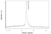
得られたZnGa2O4薄膜についてXRD(X線回折法)によるθ-2θ測定を行った。図2にZnGa2O4薄膜のXRD測定の回折パターンを示す。その結果、(222)面で配向したスピネル型のZnGa2O4のパターンを確認でき、得られたZnGa2O4薄膜はスピネル型のZnGa2O4薄膜であることが示された。 The obtained ZnGa 2 O 4 thin film was subjected to θ-2θ measurement by XRD (X-ray diffraction method). FIG. 2 shows the diffraction pattern of the ZnGa 2 O 4 thin film measured by XRD. As a result, a spinel-type ZnGa 2 O 4 pattern oriented in the (222) plane was confirmed, indicating that the obtained ZnGa 2 O 4 thin film was a spinel-type ZnGa 2 O 4 thin film.
次いで、上述のスピネル型のZnGa2O4薄膜を半導体層として用いた薄膜トランジスタを作製した。基板としてn型ドープ(リンドープ)されたシリコンウエハに150nmの熱酸化膜が形成されたものを用い、この熱酸化膜上に上記の成膜条件でZnGa2O4を成膜した。 Next, a thin film transistor was fabricated using the spinel type ZnGa 2 O 4 thin film as a semiconductor layer. A 150 nm thermal oxide film formed on an n-type doped (phosphorus-doped) silicon wafer was used as a substrate, and a ZnGa 2 O 4 film was formed on the thermal oxide film under the above film formation conditions.
そして、ソース・ドレイン電極となるCu電極をスパッタ法で成膜し、基板のシリコンウエハをゲート電極、熱酸化膜をゲート絶縁膜とすることで、半導体装置を得た。得られた半導体装置の半導体特性を半導体パラメータアナライザー(4200-SCS、KEITHLEY社製)を用いてトランジスタ特性を測定した。その結果を図3に示す。図3において、横軸はゲート電極に印加した電圧を示し、縦軸はドレイン電極で検出された電流値を示す。図3に示されるように、本実施例の半導体装置は、n型の半導体特性を示すことが確認された。また、本実施例の半導体装置は、移動度:1.1cm2/V・s、キャリア密度:1×1017cm-3、On/Off比:1×105の特性を示した。 Then, a semiconductor device was obtained by forming Cu electrodes that would become source and drain electrodes by sputtering, using the silicon wafer as a substrate as a gate electrode, and using a thermal oxide film as a gate insulating film. The semiconductor characteristics of the obtained semiconductor device were measured for transistor characteristics using a semiconductor parameter analyzer (4200-SCS, manufactured by KEITHLEY). The results are shown in FIG. In FIG. 3, the horizontal axis represents the voltage applied to the gate electrode, and the vertical axis represents the current value detected at the drain electrode. As shown in FIG. 3, it was confirmed that the semiconductor device of this example exhibited n-type semiconductor characteristics. Further, the semiconductor device of this example exhibited characteristics of mobility: 1.1 cm 2 /V·s, carrier density: 1×10 17 cm −3 , and On/Off ratio: 1×10 5 .
(pHセンサ)
(実験a)
上記で得られた半導体装置を用いてpHセンサ(Ion Sensitive-FET;イオン感応性電界効果型トランジスタ)を作製した。図4に、pHセンサの概略構成図を示す。pHセンサBは、ベース層12上に熱酸化膜14が形成されたシリコン製の基板10と、基板10上に設けられた半導体層(ZnGa2O4:H2)40とAg電極70、71とを有する半導体装置と、半導体装置上に設けられたシリコンゴム製のプール80と、プール80内に設けられた参照電極90とを有している。なお、参照電極90としてはAg/AgCl電極(銀-塩化銀電極)を用いた。そして、測定対象である溶液S(酸性溶液の場合は塩酸、アルカリ性溶液の場合は水酸化ナトリウム溶液)をプール80に入れ、参照電極90とAg電極71との電位差を測定した。なお、溶液SとしてpH1、pH7、pH14に調製された溶液を用意し、各溶液をプール80に入れた1秒後に測定を開始した。参照電極90とAg電極71との電位差は溶液中のプロトン濃度に依存する。当該電位差を測定することにより溶液中のプロトン濃度を求め、pH値として算出するのがpHセンサの測定原理である。
(pH sensor)
(Experiment a)
A pH sensor (Ion Sensitive-FET; ion-sensitive field effect transistor) was manufactured using the semiconductor device obtained above. FIG. 4 shows a schematic configuration diagram of the pH sensor. The pH sensor B includes a
図5に実施例1のpHセンサの測定結果を表すグラフを示す。横軸は時間を表し、縦軸は参照電極90とAg電極71との間の電位差を表している。図5に示すように、pH1やpH14の溶液であっても、時間とともに測定値(pH値)が大きく変化することはなく、長時間にわたり安定して測定できることが確認された。また、溶液Sをプール80に入れた1秒後に測定を開始したが、1秒後であっても電位差を検出しており、高速な応答が得られることも確認された。
FIG. 5 shows a graph showing the measurement results of the pH sensor of Example 1. The horizontal axis represents time, and the vertical axis represents the potential difference between the
(実験b)
実験aのpH1の溶液Sの測定後、半導体層40とAg電極70、71を水で洗浄し、pH1の溶液Sを用いて再度同様の測定実験を行った。その結果、同様の値が得られ、再現性のあることが確認された。また、pH14の溶液Sの測定後、半導体層40とAg電極70、71を水で洗浄し、pH14の溶液Sを用いて再度同様の測定実験を行った。その結果、同様の値が得られ、再現性のあることが確認された。実験bの結果から、本実施例のpHセンサの測定値に再現性のあることが確認されたとともに、pH1やpH14の強酸性・強塩基性の条件下であってもpHセンサの半導体層40が浸食されることなく安定して繰り返し使用できることが確認された。
(Experiment b)
After measuring the solution S at pH 1 in experiment a, the
以上より、本pHセンサは半導体層を保護するための絶縁膜を有していないにもかかわらず、高感度で高速かつ安定したpH測定が可能であることが確認された。 From the above, it was confirmed that this pH sensor is capable of high-sensitivity, high-speed, and stable pH measurement even though it does not have an insulating film to protect the semiconductor layer.
<比較例1~5>
亜鉛(Zn)とガリウム(Ga)とを含むスピネル型の酸化物(実施例1)及びそれ以外の酸化物として表1に示す酸化物(比較例1~5)をそれぞれ用意して、pH1~6の溶液中での安定性を評価した。具体的には、以下の要領で実験を行った。
pH1、2、3、4、5、6の塩酸をそれぞれ準備し、それらを各酸化物半導体の表面に1mL滴下し、室温、1気圧の条件下で10分間静置した。そして、下記の基準に基づき目視にて表面の安定性を評価した。
○:表面の変化が全く無かった。
△:溶液により表面が一部浸食された。
×:溶液により表面が浸食された。
<Comparative Examples 1 to 5>
A spinel-type oxide containing zinc (Zn) and gallium (Ga) (Example 1) and other oxides shown in Table 1 (Comparative Examples 1 to 5) were prepared, and the pH was 1 to 1. The stability of No. 6 in solution was evaluated. Specifically, the experiment was conducted in the following manner.
Hydrochloric acid having pH of 1, 2, 3, 4, 5, and 6 was prepared, and 1 mL of each of them was dropped onto the surface of each oxide semiconductor, and the mixture was left standing at room temperature and 1 atm for 10 minutes. Then, the stability of the surface was visually evaluated based on the following criteria.
○: There was no change in the surface at all.
Δ: Part of the surface was eroded by the solution.
×: The surface was eroded by the solution.

表1から明らかなように、実施例1は、pH1~6の全ての領域において表面浸食が起こらず、強酸に対して高い耐性を有していることが確認された。 As is clear from Table 1, in Example 1, surface erosion did not occur in all pH ranges of 1 to 6, and it was confirmed that it had high resistance to strong acids.
10…基板、12…ベース層、14…熱酸化膜、20…ゲート電極、30…絶縁層、40…半導体層、52…第1の電極、54…第2の電極、60…パッシベーション層、70、71…Ag電極、80…プール、90…参照電極、A…半導体装置、B…pHセンサ、S…溶液
DESCRIPTION OF
Claims (12)
前記半導体層上に導電層を形成する工程と、
前記導電層を所定のパターンに対応させて前記半導体層が露出するまでエッチングし、第1の電極及び第2の電極を形成する工程と、
を含み、
前記半導体層は、スピネル型のZnGa2O4であり、
前記エッチングを酸性溶液で行う半導体装置の製造方法を備える、pHセンサの製造方法。 a step of forming a semiconductor layer;
forming a conductive layer on the semiconductor layer;
etching the conductive layer in a predetermined pattern until the semiconductor layer is exposed, forming a first electrode and a second electrode;
including;
The semiconductor layer is spinel type ZnGa 2 O 4 ,
A method for manufacturing a pH sensor, comprising a method for manufacturing a semiconductor device in which the etching is performed using an acidic solution.
前記半導体層は、キャリア元素がドープされている、pHセンサの製造方法。 A method for manufacturing the pH sensor according to claim 1, comprising:
The method for manufacturing a pH sensor, wherein the semiconductor layer is doped with a carrier element.
前記半導体層は、水素がドープされている、pHセンサの製造方法。 A method for manufacturing a pH sensor according to claim 1 or 2, comprising:
The method for manufacturing a pH sensor , wherein the semiconductor layer is doped with hydrogen.
前記半導体層を形成する工程は、ZnGa2O4の焼結体ターゲットとZnOの焼結体ターゲットとを用いて共スパッタリングすることを含んで行われる、pHセンサの製造方法。 A method for manufacturing a pH sensor according to any one of claims 1 to 3, comprising:
The method for manufacturing a pH sensor , wherein the step of forming the semiconductor layer includes co-sputtering using a sintered target of ZnGa 2 O 4 and a sintered target of ZnO.
前記第1の電極及び第2の電極を形成する工程は、
前記導電層上にレジスト層を形成することと、
前記レジスト層を所定のパターン光で露光した後に現像することと、
現像後に前記レジスト層に形成された開口部から露出している前記導電層を前記酸性溶液でエッチングすることと、
を含んで行われる、pHセンサの製造方法。 A method for manufacturing a pH sensor according to any one of claims 1 to 4, comprising:
The step of forming the first electrode and the second electrode includes:
forming a resist layer on the conductive layer;
Developing the resist layer after exposing it to a predetermined pattern of light;
etching the conductive layer exposed through the opening formed in the resist layer after development with the acidic solution;
A method for manufacturing a pH sensor , comprising:
前記半導体層を形成する工程を190℃以上で行う、pHセンサの製造方法。 A method for manufacturing a pH sensor according to any one of claims 1 to 5, comprising:
A method for manufacturing a pH sensor , wherein the step of forming the semiconductor layer is performed at a temperature of 190° C. or higher.
前記半導体層上に導電層を形成する工程と、forming a conductive layer on the semiconductor layer;
前記導電層を所定のパターンに対応させて前記半導体層が露出するまでエッチングし、第1の電極及び第2の電極を形成する工程と、etching the conductive layer in a predetermined pattern until the semiconductor layer is exposed, forming a first electrode and a second electrode;
を含み、including;
前記半導体層は、スピネル型のZnGaThe semiconductor layer is spinel type ZnGa. 22 OO 44 であり、and
前記エッチングを酸性溶液で行う半導体装置の製造方法を備える、バイオセンサの製造方法。A method for manufacturing a biosensor, comprising a method for manufacturing a semiconductor device in which the etching is performed using an acidic solution.
前記半導体層は、キャリア元素がドープされている、バイオセンサの製造方法。The method for manufacturing a biosensor, wherein the semiconductor layer is doped with a carrier element.
前記半導体層は、水素がドープされている、バイオセンサの製造方法。The method for manufacturing a biosensor, wherein the semiconductor layer is doped with hydrogen.
前記半導体層を形成する工程は、ZnGaIn the step of forming the semiconductor layer, ZnGa 22 OO 44 の焼結体ターゲットとZnOの焼結体ターゲットとを用いて共スパッタリングすることを含んで行われる、バイオセンサの製造方法。A method for manufacturing a biosensor, the method comprising co-sputtering using a sintered target of ZnO and a sintered target of ZnO.
前記第1の電極及び第2の電極を形成する工程は、The step of forming the first electrode and the second electrode includes:
前記導電層上にレジスト層を形成することと、forming a resist layer on the conductive layer;
前記レジスト層を所定のパターン光で露光した後に現像することと、Developing the resist layer after exposing it to a predetermined pattern of light;
現像後に前記レジスト層に形成された開口部から露出している前記導電層を前記酸性溶液でエッチングすることと、etching the conductive layer exposed through the opening formed in the resist layer after development with the acidic solution;
を含んで行われる、バイオセンサの製造方法。A method for manufacturing a biosensor, which includes:
前記半導体層を形成する工程を190℃以上で行う、バイオセンサの製造方法。A method for manufacturing a biosensor, wherein the step of forming the semiconductor layer is performed at 190° C. or higher.
Applications Claiming Priority (4)
| Application Number | Priority Date | Filing Date | Title |
|---|---|---|---|
| JP2016152721 | 2016-08-03 | ||
| JP2016152721 | 2016-08-03 | ||
| JP2018531827A JPWO2018025647A1 (en) | 2016-08-03 | 2017-07-20 | Semiconductor device, pH sensor, biosensor, and method of manufacturing semiconductor device |
| PCT/JP2017/026223 WO2018025647A1 (en) | 2016-08-03 | 2017-07-20 | Semiconductor device, ph sensor, biosensor, and method for producing semiconductor device |
Related Parent Applications (1)
| Application Number | Title | Priority Date | Filing Date |
|---|---|---|---|
| JP2018531827A Division JPWO2018025647A1 (en) | 2016-08-03 | 2017-07-20 | Semiconductor device, pH sensor, biosensor, and method of manufacturing semiconductor device |
Publications (2)
| Publication Number | Publication Date |
|---|---|
| JP2022058606A JP2022058606A (en) | 2022-04-12 |
| JP7380720B2 true JP7380720B2 (en) | 2023-11-15 |
Family
ID=61073402
Family Applications (2)
| Application Number | Title | Priority Date | Filing Date |
|---|---|---|---|
| JP2018531827A Pending JPWO2018025647A1 (en) | 2016-08-03 | 2017-07-20 | Semiconductor device, pH sensor, biosensor, and method of manufacturing semiconductor device |
| JP2022003648A Active JP7380720B2 (en) | 2016-08-03 | 2022-01-13 | Semiconductor device, pH sensor, biosensor, and method for manufacturing semiconductor device |
Family Applications Before (1)
| Application Number | Title | Priority Date | Filing Date |
|---|---|---|---|
| JP2018531827A Pending JPWO2018025647A1 (en) | 2016-08-03 | 2017-07-20 | Semiconductor device, pH sensor, biosensor, and method of manufacturing semiconductor device |
Country Status (5)
| Country | Link |
|---|---|
| US (1) | US10749035B2 (en) |
| JP (2) | JPWO2018025647A1 (en) |
| KR (1) | KR102461413B1 (en) |
| CN (1) | CN109314146B (en) |
| WO (1) | WO2018025647A1 (en) |
Families Citing this family (5)
| Publication number | Priority date | Publication date | Assignee | Title |
|---|---|---|---|---|
| WO2020174540A1 (en) * | 2019-02-25 | 2020-09-03 | 株式会社ニコン | SEMICONDUCTOR DEVICE, pH SENSOR, BIOSENSOR AND METHOD FOR PRODUCING SEMICONDUCTOR DEVICE |
| WO2021125335A1 (en) * | 2019-12-20 | 2021-06-24 | 三菱マテリアル株式会社 | Transistor sensor, and method for detecting biomaterials |
| WO2022196435A1 (en) * | 2021-03-15 | 2022-09-22 | Agc株式会社 | Thin-film transistor and method for manufacturing thin-film transistor |
| WO2022196431A1 (en) * | 2021-03-15 | 2022-09-22 | Agc株式会社 | Thin film transistor and method for producing thin film transistor |
| CN117716515A (en) * | 2021-05-26 | 2024-03-15 | 株式会社 尼康 | Semiconductor device, electronic device, pH sensor, biosensor, method for manufacturing semiconductor device, and method for manufacturing electronic device |
Citations (6)
| Publication number | Priority date | Publication date | Assignee | Title |
|---|---|---|---|---|
| JP2010166030A (en) | 2008-12-19 | 2010-07-29 | Semiconductor Energy Lab Co Ltd | Method for manufacturing transistor |
| JP2010205923A (en) | 2009-03-03 | 2010-09-16 | Fujifilm Corp | Method of manufacturing field effect transistor |
| JP2011192971A (en) | 2010-02-16 | 2011-09-29 | Ricoh Co Ltd | Field-effect transistor, display element, image display device, and system |
| JP2014111818A (en) | 2012-11-09 | 2014-06-19 | Idemitsu Kosan Co Ltd | Sputtering target, oxide semiconductor thin film, and production method of them |
| JP2015190848A (en) | 2014-03-28 | 2015-11-02 | Nltテクノロジー株式会社 | Tft ion sensor, measuring method using the same, and tft ion sensor instrument |
| JP2016015484A (en) | 2014-06-13 | 2016-01-28 | 株式会社半導体エネルギー研究所 | Semiconductor device, semiconductor device manufacturing method and electronic apparatus including semiconductor device |
Family Cites Families (5)
| Publication number | Priority date | Publication date | Assignee | Title |
|---|---|---|---|---|
| JP5244331B2 (en) * | 2007-03-26 | 2013-07-24 | 出光興産株式会社 | Amorphous oxide semiconductor thin film, manufacturing method thereof, thin film transistor manufacturing method, field effect transistor, light emitting device, display device, and sputtering target |
| RU2503085C1 (en) | 2009-12-09 | 2013-12-27 | Шарп Кабусики Кайся | Semiconductor device and method of its manufacturing |
| JP6721287B2 (en) * | 2013-07-30 | 2020-07-15 | 株式会社村田製作所 | Positive electrode for secondary battery, secondary battery, battery pack, electric vehicle, power storage system, power tool and electronic device |
| US10074576B2 (en) * | 2014-02-28 | 2018-09-11 | Semiconductor Energy Laboratory Co., Ltd. | Semiconductor memory device |
| JP2016152721A (en) | 2015-02-18 | 2016-08-22 | シャープ株式会社 | Optical power generation device |
-
2017
- 2017-07-20 KR KR1020187035914A patent/KR102461413B1/en active IP Right Grant
- 2017-07-20 CN CN201780036095.4A patent/CN109314146B/en active Active
- 2017-07-20 WO PCT/JP2017/026223 patent/WO2018025647A1/en active Application Filing
- 2017-07-20 JP JP2018531827A patent/JPWO2018025647A1/en active Pending
-
2019
- 2019-01-18 US US16/251,608 patent/US10749035B2/en active Active
-
2022
- 2022-01-13 JP JP2022003648A patent/JP7380720B2/en active Active
Patent Citations (6)
| Publication number | Priority date | Publication date | Assignee | Title |
|---|---|---|---|---|
| JP2010166030A (en) | 2008-12-19 | 2010-07-29 | Semiconductor Energy Lab Co Ltd | Method for manufacturing transistor |
| JP2010205923A (en) | 2009-03-03 | 2010-09-16 | Fujifilm Corp | Method of manufacturing field effect transistor |
| JP2011192971A (en) | 2010-02-16 | 2011-09-29 | Ricoh Co Ltd | Field-effect transistor, display element, image display device, and system |
| JP2014111818A (en) | 2012-11-09 | 2014-06-19 | Idemitsu Kosan Co Ltd | Sputtering target, oxide semiconductor thin film, and production method of them |
| JP2015190848A (en) | 2014-03-28 | 2015-11-02 | Nltテクノロジー株式会社 | Tft ion sensor, measuring method using the same, and tft ion sensor instrument |
| JP2016015484A (en) | 2014-06-13 | 2016-01-28 | 株式会社半導体エネルギー研究所 | Semiconductor device, semiconductor device manufacturing method and electronic apparatus including semiconductor device |
Also Published As
| Publication number | Publication date |
|---|---|
| US10749035B2 (en) | 2020-08-18 |
| WO2018025647A1 (en) | 2018-02-08 |
| KR102461413B1 (en) | 2022-10-31 |
| CN109314146B (en) | 2022-12-27 |
| KR20190034153A (en) | 2019-04-01 |
| CN109314146A (en) | 2019-02-05 |
| JP2022058606A (en) | 2022-04-12 |
| JPWO2018025647A1 (en) | 2019-06-20 |
| US20190181268A1 (en) | 2019-06-13 |
Similar Documents
| Publication | Publication Date | Title |
|---|---|---|
| JP7380720B2 (en) | Semiconductor device, pH sensor, biosensor, and method for manufacturing semiconductor device | |
| JP5528734B2 (en) | ELECTRONIC DEVICE AND ITS MANUFACTURING METHOD, DISPLAY DEVICE, AND SENSOR | |
| TWI427795B (en) | Field-effect transistor and field-effect transistor manufacturing method | |
| Lai et al. | pH sensitivity improvement on 8 nm thick hafnium oxide by post deposition annealing | |
| CN109196626A (en) | The manufacturing method and metallic nitrogen-oxide semiconductor film of metallic nitrogen-oxide semiconductor film | |
| US7977214B2 (en) | Method of manufacturing field-effect transistor, field-effect transistor, and method of manufacturing display device | |
| Pan et al. | Effect of postdeposition annealing on the structural and sensing characteristics of Tb2O3 and Tb2Ti2O7 sensing films for electrolyte-insulator-semiconductor pH sensors | |
| Chou et al. | Fabrication and application of ruthenium-doped titanium dioxide films as electrode material for ion-sensitive extended-gate FETs | |
| WO2022249872A1 (en) | SEMICONDUCTOR APPARATUS, ELECTRONIC DEVICE, pH SENSOR, BIOSENSOR, PRODUCTION METHOD FOR SEMICONDUCTOR APPARATUS, AND PRODUCTION METHOD FOR ELECTRONIC DEVICE | |
| Pan et al. | Influence of oxygen content on the structural and sensing characteristics of Y2O3 sensing membrane for pH-ISFET | |
| Pan et al. | Yb2O3 thin films as a sensing membrane for pH-ISFET application | |
| TWI815991B (en) | Semiconductor device, pH sensor and biosensor, and method of manufacturing semiconductor device | |
| Rosdan et al. | Sputtered titanium dioxide thin film for Extended-Gate FET sensor application | |
| WO2002077632A1 (en) | Field-effect transistor | |
| Pan et al. | Structural and sensing properties of high-k Lu2O3 electrolyte-insulator-semiconductor pH sensors | |
| Bag et al. | High performance sol–gel synthesized Ce 0.9 Sr 0.1 (Zr 0.53 Ti 0.47) O 4 sensing membrane for a solid-state pH sensor | |
| Pan et al. | High-κ Dy2TiO5 Electrolyte-Insulator-Semiconductor Urea Biosensors | |
| Pan et al. | High-Performance Electrolyte–Insulator–Semiconductor pH Sensors Using High-$ k $ CeO 2 Sensing Films | |
| Singh et al. | Influence of annealing temperature on structural compositions and pH sensing properties of sol-gel derived YTixOy electroceramic sensing membranes | |
| Lo et al. | Gas sensing ability on polycrystalline-silicon nanowire | |
| Kumar et al. | Effect of post deposition annealing temperature of e-beam evaporated Ta 2 O 5 films on sensitivities of electrolyte-insulator-semiconductor devices | |
| Chen et al. | pH Sensing of Ba0. 7Sr0. 3TiO3∕ SiO2 Film for Metal-Oxide-Semiconductor and Ion-Sensitive Field-Effect Transistor Devices | |
| Pan et al. | Effect of tantalum content on the structural properties and sensing performance of YbTaxOy electrolyte-insulator-semiconductor pH sensors | |
| Pan et al. | Thin Sm2TiO5 film electrolyte–insulator–semiconductor for pH detection and urea biosensing | |
| Pan et al. | Structural properties and sensing characteristics of thin Nd2O3 sensing films for pH detection |
Legal Events
| Date | Code | Title | Description |
|---|---|---|---|
| A521 | Request for written amendment filed |
Free format text: JAPANESE INTERMEDIATE CODE: A523 Effective date: 20220113 |
|
| A621 | Written request for application examination |
Free format text: JAPANESE INTERMEDIATE CODE: A621 Effective date: 20220113 |
|
| A131 | Notification of reasons for refusal |
Free format text: JAPANESE INTERMEDIATE CODE: A131 Effective date: 20230110 |
|
| A02 | Decision of refusal |
Free format text: JAPANESE INTERMEDIATE CODE: A02 Effective date: 20230530 |
|
| A521 | Request for written amendment filed |
Free format text: JAPANESE INTERMEDIATE CODE: A523 Effective date: 20230828 |
|
| A911 | Transfer to examiner for re-examination before appeal (zenchi) |
Free format text: JAPANESE INTERMEDIATE CODE: A911 Effective date: 20230905 |
|
| TRDD | Decision of grant or rejection written | ||
| A01 | Written decision to grant a patent or to grant a registration (utility model) |
Free format text: JAPANESE INTERMEDIATE CODE: A01 Effective date: 20231003 |
|
| A61 | First payment of annual fees (during grant procedure) |
Free format text: JAPANESE INTERMEDIATE CODE: A61 Effective date: 20231016 |
|
| R150 | Certificate of patent or registration of utility model |
Ref document number: 7380720 Country of ref document: JP Free format text: JAPANESE INTERMEDIATE CODE: R150 |