JP7368552B1 - Information processing device and control method - Google Patents
Information processing device and control method Download PDFInfo
- Publication number
- JP7368552B1 JP7368552B1 JP2022100814A JP2022100814A JP7368552B1 JP 7368552 B1 JP7368552 B1 JP 7368552B1 JP 2022100814 A JP2022100814 A JP 2022100814A JP 2022100814 A JP2022100814 A JP 2022100814A JP 7368552 B1 JP7368552 B1 JP 7368552B1
- Authority
- JP
- Japan
- Prior art keywords
- processing
- module
- bios
- post time
- information
- Prior art date
- Legal status (The legal status is an assumption and is not a legal conclusion. Google has not performed a legal analysis and makes no representation as to the accuracy of the status listed.)
- Active
Links
Images


Classifications
-
- G—PHYSICS
- G06—COMPUTING OR CALCULATING; COUNTING
- G06F—ELECTRIC DIGITAL DATA PROCESSING
- G06F11/00—Error detection; Error correction; Monitoring
- G06F11/07—Responding to the occurrence of a fault, e.g. fault tolerance
- G06F11/14—Error detection or correction of the data by redundancy in operations
- G06F11/1402—Saving, restoring, recovering or retrying
- G06F11/1415—Saving, restoring, recovering or retrying at system level
- G06F11/142—Reconfiguring to eliminate the error
-
- G—PHYSICS
- G06—COMPUTING OR CALCULATING; COUNTING
- G06F—ELECTRIC DIGITAL DATA PROCESSING
- G06F11/00—Error detection; Error correction; Monitoring
- G06F11/07—Responding to the occurrence of a fault, e.g. fault tolerance
- G06F11/14—Error detection or correction of the data by redundancy in operations
- G06F11/1402—Saving, restoring, recovering or retrying
- G06F11/1415—Saving, restoring, recovering or retrying at system level
- G06F11/1417—Boot up procedures
-
- G—PHYSICS
- G06—COMPUTING OR CALCULATING; COUNTING
- G06F—ELECTRIC DIGITAL DATA PROCESSING
- G06F11/00—Error detection; Error correction; Monitoring
- G06F11/22—Detection or location of defective computer hardware by testing during standby operation or during idle time, e.g. start-up testing
- G06F11/2284—Detection or location of defective computer hardware by testing during standby operation or during idle time, e.g. start-up testing by power-on test, e.g. power-on self test [POST]
-
- G—PHYSICS
- G06—COMPUTING OR CALCULATING; COUNTING
- G06F—ELECTRIC DIGITAL DATA PROCESSING
- G06F9/00—Arrangements for program control, e.g. control units
- G06F9/06—Arrangements for program control, e.g. control units using stored programs, i.e. using an internal store of processing equipment to receive or retain programs
- G06F9/44—Arrangements for executing specific programs
- G06F9/4401—Bootstrapping
- G06F9/4403—Processor initialisation
-
- G—PHYSICS
- G06—COMPUTING OR CALCULATING; COUNTING
- G06F—ELECTRIC DIGITAL DATA PROCESSING
- G06F2201/00—Indexing scheme relating to error detection, to error correction, and to monitoring
- G06F2201/865—Monitoring of software
Landscapes
- Engineering & Computer Science (AREA)
- Theoretical Computer Science (AREA)
- General Engineering & Computer Science (AREA)
- Physics & Mathematics (AREA)
- General Physics & Mathematics (AREA)
- Software Systems (AREA)
- Quality & Reliability (AREA)
- Computer Security & Cryptography (AREA)
- Computer Hardware Design (AREA)
- Debugging And Monitoring (AREA)
- Test And Diagnosis Of Digital Computers (AREA)
Abstract
【課題】BIOSにより起動する際に、異常箇所を適切に特定する。
【解決手段】情報処理装置は、BIOSの部分機能を示すモジュールを識別するモジュール識別情報と、当該モジュールに対してのPOST処理に要する処理時間を示すPOST時間の基準値とを対応付けて記憶する基準POST時間記憶部と、前記BIOSに基づく処理を実行するBIOS処理部であって、前記BIOSの設定に応じた前記モジュールごとに前記POST処理を実行し、実行した前記モジュールごとの前記POST時間を測定する処理と、前記モジュールに対して測定した前記POST時間と、前記基準POST時間記憶部が記憶する当該モジュールの前記モジュール識別情報に対応する前記基準値とに基づいて、前記POST時間が増大しているか否かを判定し、異常のある前記モジュールである異常モジュールを特定する処理とを実行するBIOS処理部とを備える。
【選択図】図2
An object of the present invention is to appropriately identify abnormalities when starting up with BIOS.
[Solution] An information processing device stores module identification information that identifies a module indicating a partial function of a BIOS, and a reference value of POST time indicating the processing time required for POST processing for the module in association with each other. a reference POST time storage unit, and a BIOS processing unit that executes processing based on the BIOS, which executes the POST processing for each module according to the BIOS settings, and stores the POST time for each executed module. The POST time increases based on the process to be measured, the POST time measured for the module, and the reference value corresponding to the module identification information of the module stored in the reference POST time storage unit. and a BIOS processing unit that executes a process of determining whether or not the module is abnormal, and identifying an abnormal module that is the module with an abnormality.
[Selection diagram] Figure 2
Description
本発明は、情報処理装置、及び制御方法に関する。 The present invention relates to an information processing device and a control method.
従来、パーソナルコンピュータ(PC)などの情報処理装置では、BIOS(Basic Input Output System)が実行されることにより、情報処理装置の初期化及びOS(Operating System)の起動を行っている。また、従来の情報処理装置では、BIOSを実行して起動する際に、POST(Power On Self Test)処理という診断テストを実行している。 BACKGROUND ART Conventionally, in an information processing device such as a personal computer (PC), a BIOS (Basic Input Output System) is executed to initialize the information processing device and start up an OS (Operating System). Further, in the conventional information processing apparatus, when the BIOS is executed and started, a diagnostic test called POST (Power On Self Test) processing is executed.
ところで、情報処理装置では、BIOSの設定に応じたBIOS内のモジュールに対して、POST処理が実行されるが、情報処理装置が内蔵するデバイスの劣化や故障によって、POST処理の期間であるPOST時間が長くなることがある。しかしながら、従来の情報処理装置では、このようにPOST時間が長くなった場合に、POST時間が長くなったモジュールを特定し、異常の原因を推定することが困難であった。 By the way, in an information processing device, POST processing is executed for a module in the BIOS according to the BIOS settings, but due to deterioration or failure of a device built into the information processing device, the POST time, which is the period of POST processing, may be delayed. may be long. However, in conventional information processing devices, when the POST time becomes long in this way, it is difficult to specify the module whose POST time is long and to estimate the cause of the abnormality.
本発明は、上記問題を解決すべくなされたもので、その目的は、BIOSにより起動する際に、異常箇所を適切に特定することができる情報処理装置、及び制御方法を提供することにある。 The present invention has been made to solve the above-mentioned problems, and its purpose is to provide an information processing device and a control method that can appropriately identify abnormalities when booted by BIOS.
上記問題を解決するために、本発明の一態様は、BIOS(Basic Input Output System)の部分機能を示すモジュールを識別するモジュール識別情報と、当該モジュールに対してのPOST(Power On Self Test)処理に要する処理時間を示すPOST時間の基準値とを対応付けて記憶する基準POST時間記憶部と、前記BIOSに基づく処理を実行するBIOS処理部であって、前記BIOSの設定に応じた前記モジュールごとに前記POST処理を実行し、実行した前記モジュールごとの前記POST時間を測定する処理と、前記モジュールに対して測定した前記POST時間と、前記基準POST時間記憶部が記憶する当該モジュールの前記モジュール識別情報に対応する前記基準値とに基づいて、前記POST時間が増大しているか否かを判定し、異常のある前記モジュールである異常モジュールを特定する処理とを実行するBIOS処理部とを備え、前記BIOS処理部は、前記モジュールに異常があると特定された場合に、前記POST時間が、徐々に増加した漸増と急激に増加した急増とのいずれかであるかと、当該モジュールがソフトウェアとハードウェアとのいずれに関連するのかとに基づいて、前記異常モジュールをカテゴリに分類し、分類したカテゴリに基づいて、異常の原因を推定する情報処理装置である。 In order to solve the above problem, one aspect of the present invention provides module identification information that identifies a module indicating a partial function of a BIOS (Basic Input Output System) and a POST (Power On Self Test) process for the module. a reference POST time storage unit that stores a reference value of POST time in association with a reference value of a POST time indicating the processing time required for the process; and a BIOS processing unit that executes processing based on the BIOS, for each module according to the settings of the BIOS. a process of executing the POST process and measuring the POST time for each of the executed modules; the POST time measured for the module; and the module identification of the module stored in the reference POST time storage unit. a BIOS processing unit that determines whether or not the POST time has increased based on the reference value corresponding to the information, and executes a process of identifying an abnormal module that is the module with an abnormality , When the module is identified as having an abnormality, the BIOS processing unit determines whether the POST time is either a gradual increase or a sudden increase, and whether the module is software and hardware. The information processing apparatus classifies the abnormal module into categories based on which of the above is related to the abnormal module, and estimates the cause of the abnormality based on the classified categories.
また、本発明の一態様は、上記の情報処理装置において、前記BIOS処理部は、今回測定した前記POST時間と、前回の前記POST時間との差分値と、過去の前記差分値の平均値とに基づいて、前記POST時間が前記漸増と前記急増とのいずれかであるかを判定してもよい。 Further, in one aspect of the present invention, in the above information processing device, the BIOS processing unit calculates a difference value between the currently measured POST time and the previous POST time, and an average value of the past difference values. Based on this, it may be determined whether the POST time is either the gradual increase or the rapid increase.
また、本発明の一態様は、上記の情報処理装置において、前記BIOSの設定変更及び内蔵デバイスの変更を含む前記BIOSの環境変更に関する変更履歴を記憶する変更履歴記憶部を備え、前記BIOS処理部は、前記変更履歴記憶部から、前記異常モジュールに関連する前記変更履歴を取得し、前記異常モジュールに関連する前記変更履歴と、前記カテゴリとに基づいて、前記異常の原因を推定してもよい。 Further, in one aspect of the present invention, the information processing apparatus described above includes a change history storage unit that stores a change history regarding environment changes of the BIOS including changes in settings of the BIOS and changes in built-in devices; may acquire the change history related to the abnormal module from the change history storage unit, and estimate the cause of the abnormality based on the change history related to the abnormal module and the category. .
また、本発明の一態様は、上記の情報処理装置において、前記カテゴリと、前記異常の原因と、対応処理を示す対応処理情報とを対応付けて記憶する対応処理記憶部を備え、前記BIOS処理部は、前記カテゴリ及び前記異常の原因に対応する前記対応処理情報を、前記対応処理記憶部から取得し、取得した前記対応処理情報に基づく対応処理を実行してもよい。 Further, in one aspect of the present invention, the above-mentioned information processing apparatus includes a corresponding processing storage unit that stores the category, the cause of the abnormality, and corresponding processing information indicating the corresponding processing in association with each other, and the BIOS processing The unit may acquire the response process information corresponding to the category and the cause of the abnormality from the response process storage unit, and execute the response process based on the acquired response process information.
また、本発明の一態様は、上記の情報処理装置において、前記対応処理情報には、前記BIOSの環境を変更前に戻すロールバック処理を示すロールバック処理情報が含まれ、前記BIOS処理部は、前記カテゴリ及び前記異常の原因に対応する前記対応処理情報が、前記ロールバック処理情報である場合に、前記ロールバック処理情報に基づく前記ロールバック処理を実行してもよい。 Further, in one aspect of the present invention, in the above information processing device, the corresponding processing information includes rollback processing information indicating rollback processing to return the BIOS environment to the state before the change, and the BIOS processing unit , when the corresponding processing information corresponding to the category and the cause of the abnormality is the rollback processing information, the rollback processing may be executed based on the rollback processing information.
また、本発明の一態様は、上記の情報処理装置において、前記対応処理情報には、前記BIOSの環境を復旧するリカバリ処理を示すリカバリ処理情報が含まれ、前記BIOS処理部は、前記カテゴリ及び前記異常の原因に対応する前記対応処理情報が、前記リカバリ処理情報である場合に、前記リカバリ処理情報に基づく前記リカバリ処理を実行してもよい。 Further, in one aspect of the present invention, in the above information processing apparatus, the corresponding processing information includes recovery processing information indicating recovery processing for restoring the BIOS environment, and the BIOS processing unit is configured to When the response processing information corresponding to the cause of the abnormality is the recovery processing information, the recovery processing may be performed based on the recovery processing information.
また、本発明の一態様は、BIOS(Basic Input Output System)の部分機能を示すモジュールを識別するモジュール識別情報と、当該モジュールに対してのPOST(Power On Self Test)処理に要する処理時間を示すPOST時間の基準値とを対応付けて記憶する基準POST時間記憶部と、前記BIOSに基づく処理を実行するBIOS処理部とを備える情報処理装置の制御方法であって、前記BIOS処理部が、前記BIOSの設定に応じた前記モジュールごとに前記POST処理を実行し、実行した前記モジュールごとの前記POST時間を測定するステップと、前記BIOS処理部が、前記モジュールに対して測定した前記POST時間と、前記基準POST時間記憶部が記憶する当該モジュールの前記モジュール識別情報に対応する前記基準値とに基づいて、前記POST時間が増大しているか否かを判定し、異常のある前記モジュールである異常モジュールを特定するステップと、前記BIOS処理部が、前記モジュールに異常があると特定された場合に、前記POST時間が、徐々に増加した漸増と急激に増加した急増とのいずれかであるかと、当該モジュールがソフトウェアとハードウェアとのいずれに関連するのかとに基づいて、前記異常モジュールをカテゴリに分類し、分類したカテゴリに基づいて、異常の原因を推定するステップとを含む制御方法である。 Further, one aspect of the present invention provides module identification information that identifies a module indicating a partial function of a BIOS (Basic Input Output System) and a processing time required for POST (Power On Self Test) processing for the module. A method for controlling an information processing apparatus, comprising: a reference POST time storage unit that stores a reference value of a POST time in association with a reference value; and a BIOS processing unit that executes processing based on the BIOS, the BIOS processing unit executing the POST process for each module according to BIOS settings, and measuring the POST time for each executed module; and the POST time measured by the BIOS processing unit for the module; Based on the reference value corresponding to the module identification information of the module stored in the reference POST time storage unit, it is determined whether or not the POST time is increasing, and the abnormal module that is the module with the abnormality is determined. and determining whether the POST time is either a gradual increase or a rapid increase when the BIOS processing unit identifies that the module has an abnormality. This control method includes the steps of classifying the abnormal module into categories based on whether the module is related to software or hardware, and estimating the cause of the abnormality based on the classified category.
本発明の上記態様によれば、BIOSにより起動する際に、異常箇所を適切に特定することができる。 According to the above aspect of the present invention, an abnormal location can be appropriately identified when booting by BIOS.
以下、本発明の一実施形態による情報処理装置、及び制御方法について、図面を参照して説明する。 Hereinafter, an information processing device and a control method according to an embodiment of the present invention will be described with reference to the drawings.
図1は、本実施形態によるノートPC1の主要なハードウェア構成の一例を示す図である。なお、本実施形態において、情報処理装置の一例として、ノートPC1について説明する。 FIG. 1 is a diagram showing an example of the main hardware configuration of a notebook PC 1 according to this embodiment. Note that in this embodiment, a notebook PC 1 will be described as an example of an information processing device.
図1に示すように、ノートPC1は、CPU11と、メインメモリ12と、ビデオサブシステム13と、表示部14と、チップセット21と、BIOSメモリ22と、HDD23と、オーディオシステム24と、WLANカード25と、USBコネクタ26と、エンベデッドコントローラ31と、入力部32と、電源回路33とを備える。
なお、本実施形態において、CPU11と、チップセット21とは、メイン制御部10に対応する。また、メイン制御部10は、メモリ(メインメモリ12)に記憶されたプログラムを実行するプロセッサ(メインプロセッサ)の一例である。
As shown in FIG. 1, the notebook PC 1 includes a
Note that in this embodiment, the
CPU(Central Processing Unit)11は、プログラム制御により種々の演算処理を実行し、ノートPC1全体を制御している。
メインメモリ12は、CPU11の実行プログラムの読み込み領域として、又は、実行プログラムの処理データを書き込む作業領域として利用される書き込み可能メモリである。メインメモリ12は、例えば、複数個のDRAM(Dynamic Random Access Memory)チップで構成される。この実行プログラムには、BIOS(Basic Input Output System)、OS、周辺機器類をハードウェア操作するための各種ドライバ、各種サービス/ユーティリティ、アプリケーションプログラム等が含まれる。
A CPU (Central Processing Unit) 11 executes various calculation processes under program control and controls the entire notebook PC 1 .
The
ビデオサブシステム13は、画像表示に関連する機能を実現するためのサブシステムであり、ビデオコントローラを含んでいる。このビデオコントローラは、CPU11からの描画命令を処理し、処理した描画情報をビデオメモリに書き込むとともに、ビデオメモリからこの描画情報を読み出して、表示部14に描画データ(表示データ)として出力する。
表示部14は、例えば、液晶ディスプレイであり、ビデオサブシステム13から出力された描画データ(表示データ)に基づく表示画面を表示する。
The
The
チップセット21は、USB(Universal Serial Bus)、シリアルATA(AT Attachment)、SPI(Serial Peripheral Interface)バス、PCI(Peripheral Component Interconnect)バス、PCI-Expressバス、及びLPC(Low Pin Count)バスなどのコントローラを備えており複数のデバイスが接続される。図1では、デバイスの例示として、BIOSメモリ22と、HDD23と、オーディオシステム24と、WLANカード25と、USBコネクタ26とが、チップセット21に接続されている。
The
BIOSメモリ22は、例えば、EEPROM(Electrically Erasable Programmable Read Only Memory)やフラッシュROMなどの電気的に書き換え可能な不揮発性メモリで構成される。BIOSメモリ22は、BIOS、及びエンベデッドコントローラ31などを制御するためのシステムファームウェアなどを記憶する。
The
HDD(Hard Disk Drive)23(不揮発性記憶装置の一例)は、OS、各種ドライバ、各種サービス/ユーティリティ、アプリケーションプログラム、及び各種データを記憶する。
オーディオシステム24は、音データの記録、再生、出力を行う。
The HDD (Hard Disk Drive) 23 (an example of a nonvolatile storage device) stores an OS, various drivers, various services/utilities, application programs, and various data.
The
WLAN(Wireless Local Area Network)カード25は、ワイヤレス(無線)LANにより、ネットワークに接続して、データ通信を行う。
USBコネクタ26は、USBを利用した周辺機器類を接続するためのコネクタである。
A WLAN (Wireless Local Area Network)
The
エンベデッドコントローラ31(サブ制御部の一例)は、ノートPC1のシステム状態に関わらず、各種デバイス(周辺装置やセンサ等)を監視し制御するワンチップマイコン(One-Chip Microcomputer)である。また、エンベデッドコントローラ31は、電源回路33を制御する電源管理機能を有している。なお、エンベデッドコントローラ31は、不図示のCPU、ROM、RAMなどで構成されるとともに、複数チャネルのA/D入力端子、D/A出力端子、タイマ、及びデジタル入出力端子を備えている。エンベデッドコントローラ31には、それらの入出力端子を介して、例えば、入力部32、及び電源回路33などが接続されており、エンベデッドコントローラ31は、これらの動作を制御する。
The embedded controller 31 (an example of a sub-control unit) is a one-chip microcomputer that monitors and controls various devices (peripheral devices, sensors, etc.) regardless of the system state of the notebook PC 1. Further, the embedded
入力部32は、例えば、キーボード、ポインティング・デバイス、タッチパッドなどの入力デバイスである。
電源回路33は、例えば、DC/DCコンバータ、充放電ユニット、電池ユニット、AC/DCアダプタなどを含んでおり、AC/DCアダプタ、又は電池ユニットから供給される直流電圧を、ノートPC1を動作させるために必要な複数の電圧に変換する。また、電源回路33は、エンベデッドコントローラ31からの制御に基づいて、ノートPC1の各部に電力を供給する。
The
The
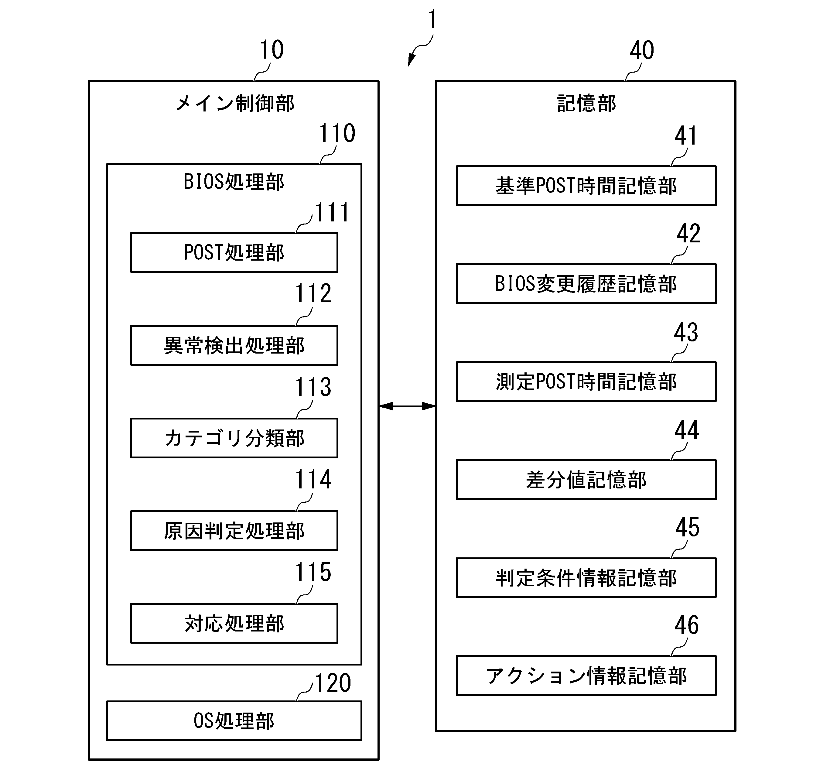
次に、図2を参照して、本実施形態によるノートPC1の機能構成について説明する。
図2は、本実施形態によるノートPC1の機能構成の一例を示す機能ブロック図である。なお、図2では、ノートPC1が備える機能構成のうち、本発明に関連する構成のみを記載している。
Next, with reference to FIG. 2, the functional configuration of the
FIG. 2 is a functional block diagram showing an example of the functional configuration of the
図2に示すように、ノートPC1は、メイン制御部10と、記憶部40とを備える。
記憶部40は、例えば、BIOSメモリ22により実現される記憶部であり、例えば、BIOSに関連する情報を記憶する。なお、BIOSの設定は、記憶部40に記憶されているものとする。
また、記憶部40は、基準POST時間記憶部41と、BIOS変更履歴記憶部42と、測定POST時間記憶部43と、差分値記憶部44と、判定条件情報記憶部45と、アクション情報記憶部46とを備える。
As shown in FIG. 2, the
The
The
基準POST時間記憶部41は、BIOSメモリ22により実現される記憶部であり、BIOSによるPOST(Power On Self Test)処理に要する処理時間を示すPOST時間の基準値を記憶する。POST時間の基準値は、ノートPC1の工場出荷時に測定されたPOST時間に基づいて設定される。ここで、図3を参照して、基準POST時間記憶部41のデータ例について説明する。
The reference POST
図3は、本実施形態における基準POST時間記憶部41のデータ例を示す図である。
図3に示すように、基準POST時間記憶部41は、モジュール名と、基準値と、属性とを対応付けて記憶する。
ここで、モジュール名は、BIOSの部分機能を示すモジュールの名称を示している。モジュール名は、モジュールを識別するモジュール識別情報の一例である。
FIG. 3 is a diagram showing an example of data in the reference POST
As shown in FIG. 3, the reference POST
Here, the module name indicates the name of a module indicating a partial function of the BIOS. The module name is an example of module identification information that identifies a module.
また、基準値は、POST時間の基準値を示し、ノートPC1の工場出荷時に測定されたPOST時間に基づいて、モジュールごとに設定されている。なお、基準値は、ノートPC1の個体ごとに異なる値となる。
また、属性は、POST処理の内容が、ソフトウェア(S/W)に関連するのか、ハードウェア(H/W)に関連するのかを示す属性情報である。
Further, the reference value indicates a reference value of the POST time, and is set for each module based on the POST time measured when the
Further, the attribute is attribute information indicating whether the content of the POST process is related to software (S/W) or hardware (H/W).
図3に示す例では、モジュール名が“PEI Phase”の全体の基準値が“1550”(ms)であるとことを示している。また、モジュール名が“PEI Phase”内の“000-1FF”の基準値が“400”であり、属性が“S/W”であることを示している。また、“200-3FF”の基準値が“850”であり、属性が“H/W”であることを示している。 The example shown in FIG. 3 shows that the module name is "PEI Phase" and the overall reference value is "1550" (ms). Further, the reference value of "000-1FF" in the module name "PEI Phase" is "400", indicating that the attribute is "S/W". Further, the reference value of "200-3FF" is "850", indicating that the attribute is "H/W".
このように、基準POST時間記憶部41は、モジュール識別情報(モジュール名)と、POST時間の基準値とを対応付けて、全モジュール分記憶している。
In this manner, the reference POST
図2の説明に戻り、BIOS変更履歴記憶部42(変更履歴記憶部の一例)は、BIOSメモリ22により実現される記憶部であり、BIOSの設定変更及び内蔵デバイス(CPU11、メインメモリ12、HDD23など)の変更を含むBIOSの環境変更に関する変更履歴を記憶する。BIOS変更履歴記憶部42は、例えば、BIOSの設定変更や内蔵デバイスの変更のイベントログを記憶する。ここで、図4を参照して、BIOS変更履歴記憶部42のデータ例について説明する。
Returning to the explanation of FIG. 2, the BIOS change history storage unit 42 (an example of a change history storage unit) is a storage unit realized by the
図4は、本実施形態におけるBIOS変更履歴記憶部42のデータ例を示す図である。
図4に示すように、BIOS変更履歴記憶部42は、イベントと、要素とを対応付けたイベントログを記憶する。
FIG. 4 is a diagram showing an example of data in the BIOS change
As shown in FIG. 4, the BIOS change
図4において、イベントは、実行されたBIOSの設定変更や内蔵デバイスの変更のイベントの内容を示している。また、要素は、イベントに関連する要素を示している。なお、BIOS変更履歴記憶部42は、イベントログを時系列に記憶している。
In FIG. 4, the event indicates the contents of an executed BIOS setting change or built-in device change. Further, the element indicates an element related to an event. Note that the BIOS change
図4に示す例では、最初のイベントログとして、イベントが“Device Change Event”であり、要素が“HDD、Memory”であるイベントログが記憶されていることを示している。また、次のイベントログとして、イベントが“Self Healing Event”であり、要素が“BIOS、EC”であるイベントログが記憶されていることを示している。 The example shown in FIG. 4 shows that an event log in which the event is "Device Change Event" and the element is "HDD, Memory" is stored as the first event log. Furthermore, it is shown that an event log in which the event is "Self Healing Event" and the elements are "BIOS, EC" is stored as the next event log.
再び、図2の説明に戻り、測定POST時間記憶部43は、BIOSメモリ22により実現される記憶部であり、実際に測定したPOST時間を記憶する。測定POST時間記憶部43は、例えば、モジュール名と、POST時間の測定値とを対応付けて記憶する。ここで、図5を参照して、測定POST時間記憶部43のデータ例について説明する。
Returning to the explanation of FIG. 2 again, the measured POST
図5は、本実施形態における測定POST時間記憶部43のデータ例を示す図である。
図5に示すように、測定POST時間記憶部43は、モジュール名と、POST時間測定値と、過去測定値とを対応付けて記憶する。
FIG. 5 is a diagram showing an example of data in the measurement POST
As shown in FIG. 5, the measured POST
図5において、モジュール名は、モジュール識別情報の一例であり、POST時間測定値は、POST時間の測定値である。また、過去測定値は、過去の所定の回数のPOST時間の測定値を示している。 In FIG. 5, the module name is an example of module identification information, and the POST time measurement value is a measurement value of POST time. Furthermore, the past measurement value indicates a measurement value of a predetermined number of POST times in the past.
例えば、図5に示す例では、モジュール名が“PEI Phase”の全体のPOST時間の測定値が、“1555”(ms)であり、過去測定値として、1回前が“1552”(ms)、2回前が“1550”(ms)、3回前が“1554”(ms)であることを示している。また、“000-1FF”の部分のPOST時間の測定値が、“402”(ms)であり、過去測定値として、1回前が“401”(ms)、2回前が“400”(ms)、3回前が“402”(ms)であることを示している。 For example, in the example shown in FIG. 5, the measured value of the entire POST time of the module name "PEI Phase" is "1555" (ms), and the previous measured value is "1552" (ms). , the second time ago is "1550" (ms), and the third time ago is "1554" (ms). In addition, the measured value of the POST time in the "000-1FF" part is "402" (ms), and the past measured values are "401" (ms) the first time and "400" (the second time). ms), and the third time before is "402" (ms).
また、“200-3FF”の部分のPOST時間の測定値が、“852”(ms)であり、過去測定値として、1回前が“851”(ms)、2回前が“850”(ms)、3回前が“851”(ms)であることを示している。また、“400-5FF”の部分のPOST時間の測定値が、“300”(ms)であり、過去測定値として、1回前が“300”(ms)、2回前が“300”(ms)、3回前が“301”(ms)であることを示している。 Also, the measured value of the POST time of the "200-3FF" part is "852" (ms), and the past measured values are "851" (ms) the first time and "850" (second time). ms), and the third time before is "851" (ms). Also, the measured value of the POST time in the "400-5FF" part is "300" (ms), and the past measured values are "300" (ms) the first time and "300" (ms) the second time. ms), and the third time before is "301" (ms).
再び、図2の説明に戻り、差分値記憶部44は、BIOSメモリ22により実現される記憶部であり、今回測定したPOST時間と、前回測定したPOST時間との差分値と、当該差分値の所定の回数分の平均値とを記憶する。ここで、図6を参照して、差分値記憶部44のデータ例について説明する。
Returning to the explanation of FIG. 2 again, the difference
図6は、本実施形態における差分値記憶部44のデータ例を示す図である。
図6に示すように、差分値記憶部44は、モジュール名と、差分値と、差分平均値とを対応付けて記憶する。
FIG. 6 is a diagram showing an example of data in the difference
As shown in FIG. 6, the difference
図6において、モジュール名は、モジュール識別情報の一例であり、差分値は、今回測定したPOST時間と、前回のPOST時間との差分値を示している。また、差分平均値は、過去の所定回数分の差分値の平均値を示している。 In FIG. 6, the module name is an example of module identification information, and the difference value indicates the difference value between the currently measured POST time and the previous POST time. Further, the average difference value indicates the average value of the difference values for a predetermined number of times in the past.
例えば、図6に示す例では、モジュール名が“PEI Phase”の差分値が、“10”(ms)であり、差分平均値が“10”(ms)であることを示している。また、“000-1FF”の部分の差分値が、“0”(ms)であり、差分平均値が“0”(ms)であることを示している。 For example, in the example shown in FIG. 6, the difference value of the module name "PEI Phase" is "10" (ms), and the average difference value is "10" (ms). Further, the difference value of the portion "000-1FF" is "0" (ms), indicating that the average difference value is "0" (ms).
また、“200-3FF”の部分の差分値が、“10”(ms)であり、差分平均値が“10”(ms)であることを示している。また、“400-5FF”の部分の差分値が、“0”(ms)であり、差分平均値が“0”(ms)であることを示している。 Further, the difference value of the portion "200-3FF" is "10" (ms), indicating that the average difference value is "10" (ms). Further, the difference value of the portion "400-5FF" is "0" (ms), indicating that the average difference value is "0" (ms).
再び、図2の説明に戻り、判定条件情報記憶部45は、BIOSメモリ22により実現される記憶部であり、POST時間が増大した異常モジュールに対する原因の判定条件を記憶する。判定条件情報記憶部45は、例えば、POST時間の増大から異常が検出されたモジュールを分類したカテゴリとイベントログとから推定される原因を記憶する。判定条件情報記憶部45が記憶する情報は、予め記憶されているものとする。ここで、図7を参照して、判定条件情報記憶部45のデータ例について説明する。
Returning to the explanation of FIG. 2 again, the determination condition
図7は、本実施形態における判定条件情報記憶部45のデータ例を示す図である。
図7に示すように、判定条件情報記憶部45は、カテゴリ名と、小分類と、検出されたイベントと、原因とを対応付けて記憶する。
FIG. 7 is a diagram showing an example of data in the determination condition
As shown in FIG. 7, the determination condition
図7において、カテゴリ名は、分類したカテゴリ名を示し、小分類は、カテゴリの小分類を示している。なお、カテゴリの詳細については後述する。また、検出されたイベントは、上述したBIOS変更履歴記憶部42が記憶するイベントログのうち、直近において検出されたイベントを示している。また、原因は、異常モジュールの推定原因を示している。
In FIG. 7, the category name indicates the name of the classified category, and the subclassification indicates the subclassification of the category. Note that the details of the categories will be described later. Further, the detected event indicates the most recently detected event among the event logs stored in the BIOS change
図7に示す例では、カテゴリ名が“A(S/W、急増)”において、小分類“A1”として、検出されたイベントが“BIOS Setup Configuration Change Event”及び“POST Error Event”である場合に、原因が“Configuration Change”であることを示している。 In the example shown in FIG. 7, the category name is "A (S/W, rapid increase)", the subcategory is "A1", and the detected events are "BIOS Setup Configuration Change Event" and "POST Error Event". It shows that the cause is "Configuration Change".
このように、判定条件情報記憶部45は、カテゴリごとに、検出されたイベントに対して推定される原因(POST時間が増大した原因)を記憶している。
In this manner, the determination condition
再び、図2の説明に戻り、アクション情報記憶部46(対応処理記憶部の一例)は、BIOSメモリ22により実現される記憶部であり、POST時間が増大した異常モジュールの原因に対する対応処理(アクション)を示すアクションテーブルを記憶する。
Returning to the explanation of FIG. 2 again, the action information storage unit 46 (an example of a response processing storage unit) is a storage unit implemented by the
アクション情報記憶部46は、例えば、カテゴリと、異常の原因と、対応処理(アクション)を示す対応処理情報(アクション情報)とを対応付けて記憶する。アクション情報記憶部46が記憶する情報は、予め記憶されているものとする。ここで、図8を参照して、アクション情報記憶部46のデータ例について説明する。
The action
図8は、本実施形態におけるアクション情報記憶部46のデータ例を示す図である。
図8に示すように、アクション情報記憶部46は、カテゴリ名と、原因と、対応処理とを対応付けて記憶する。
FIG. 8 is a diagram showing an example of data in the action
As shown in FIG. 8, the action
図8において、カテゴリ名は、カテゴリを識別するカテゴリ識別情報の一例である。また、原因は、POST時間が増大した異常モジュールの推定原因を示し、対応処理は、原因に対する対応処理(アクション)を示している。 In FIG. 8, the category name is an example of category identification information that identifies a category. Furthermore, the cause indicates the presumed cause of the abnormal module that increased the POST time, and the response process indicates a response process (action) for the cause.
図8に示す例では、カテゴリ名が“A(S/W、急増)”であり、原因が“Configuration Change”である場合に、対応処理が“Setting rollback”であることを示している。また、カテゴリ名が“A(S/W、急増)”であり、原因が“Firmware Update Event”である場合に、対応処理が“BIOS recovery”であることを示している。 The example shown in FIG. 8 shows that when the category name is "A (S/W, rapid increase)" and the cause is "Configuration Change", the corresponding process is "Setting rollback". Further, when the category name is "A (S/W, rapid increase)" and the cause is "Firmware Update Event", it is shown that the corresponding process is "BIOS recovery".
また、カテゴリ名が“A(S/W、急増)”であり、原因が“Self Healing Event”である場合に、対応処理が“Warning Message”であることを示している。 Further, when the category name is "A (S/W, rapid increase)" and the cause is "Self Healing Event", it is shown that the corresponding process is "Warning Message".
再び、図2の説明に戻り、メイン制御部10は、CPU11及びチップセット21に、BIOSメモリ22及びHDD23が記憶するプログラムを実行させることで実現される機能部であり、BIOS又はOSに基づくノートPC1の各種処理を実行する。メイン制御部10は、BIOS処理部110と、OS処理部120とを備える。
Returning to the explanation of FIG. 2 again, the
BIOS処理部110は、CPU11及びチップセット21に、BIOSメモリ22が記憶するプログラムを実行させることで実現される機能部であり、BIOSに基づく各種処理を実行する。BIOS処理部110は、例えば、ノートPC1を起動する際に、POST処理を実行し、結果が正常である場合に、OSを起動して、後述するOS処理部120に処理を引き継ぐ。
The
また、BIOS処理部110は、BIOSの設定に応じたモジュールごとにPOST処理を実行し、実行したモジュールごとのPOST時間を測定し、POST時間が増大した異常モジュールを特定する。また、BIOS処理部110は、特定したPOST時間が増大した異常モジュールに対する原因を推定し、推定した原因に対する対応処理を実行する。
また、BIOS処理部110は、POST処理部111と、異常検出処理部112と、カテゴリ分類部113と、原因判定処理部114と、対応処理部115とを備える。
Furthermore, the
The
POST処理部111は、CPU11及びチップセット21に、BIOSメモリ22が記憶するプログラムを実行させることで実現される機能部であり、BIOSの設定に応じたモジュールごとにPOST処理を実行し、実行したモジュールごとのPOST時間を測定する処理を実行する。POST処理部111は、ノートPC1が起動する際に、モジュールごとにPOST処理を実行し、例えば、図5に示すように、モジュール名と、POST時間測定値と、過去測定値とを対応付けて、測定POST時間記憶部43に記憶させる。なお、過去測定値は、例えば、今回の測定以前の過去3回分の測定値である。
The
異常検出処理部112は、PU11及びチップセット21に、BIOSメモリ22が記憶するプログラムを実行させることで実現される機能部であり、モジュールに対して測定したPOST時間と、基準POST時間記憶部41が記憶する当該モジュールのモジュール識別情報に対応する基準値とに基づいて、POST時間が増大しているか否かを判定し、異常のあるモジュールである異常モジュールを特定する処理を実行する。ここで、異常モジュールとは、POST時間が増大したことで異常があると判定されるモジュールである。
The abnormality
異常検出処理部112は、モジュールごとに、測定POST時間記憶部43が記憶するPOST時間と、基準POST時間記憶部41が記憶する基準値とを比較して、POST時間が増大しているか否かを判定する。具体的に、異常検出処理部112は、下記の式(1)により、測定値が、(基準値+α)以上であるか否かにより、POST時間が増大しているか否かを判定する。
The abnormality
![]()
![]()
なお、ここでの“α”は、所定のマージン値である。
また、異常検出処理部112は、POST時間が増大していると判定したモジュールを異常(問題)のある異常モジュールと特定する。
Note that "α" here is a predetermined margin value.
Furthermore, the abnormality
カテゴリ分類部113は、CPU11及びチップセット21に、BIOSメモリ22が記憶するプログラムを実行させることで実現される機能部であり、モジュールに異常があると特定された場合に、異常モジュールを以下の4つのカテゴリに分類する。
The
カテゴリ“A”:S/Wに関してPOST時間が急激に増大しているもの(S/W、急増)
カテゴリ“B”:S/Wに関してPOST時間が徐々に増大しているもの(S/W、漸増)
カテゴリ“C”:H/Wに関してPOST時間が急激に増大しているもの(H/W、漸増)
カテゴリ“D”:H/Wに関してPOST時間が徐々に増大しているもの(H/W、急増)
Category “A”: S/W-related POST time is rapidly increasing (S/W, rapid increase)
Category “B”: S/W-related POST time gradually increases (S/W, gradual increase)
Category “C”: POST time increases rapidly regarding H/W (H/W, gradual increase)
Category “D”: POST time is gradually increasing regarding H/W (H/W, rapidly increasing)
すなわち、カテゴリ分類部113は、例えば、POST時間が、徐々に増加した漸増と急激に増加した急増とのいずれかであるかと、当該モジュールがソフトウェアとハードウェアとのいずれに関連するのかとに基づいて、異常モジュールをカテゴリに分類する。
That is, the
カテゴリ分類部113は、測定値tNと、前回の測定値tN-1との差分値Δt(=tN-tN-1)を算出する。カテゴリ分類部113は、例えば、測定POST時間記憶部43が記憶する情報を用いて、差分値Δtを算出する。
The
また、カテゴリ分類部113は、過去複数回の差分値Δtを用いて差分平均値を算出する。カテゴリ分類部113は、測定POST時間記憶部43が記憶する情報を用いて、差分平均値を算出する。なお、カテゴリ分類部113は、異常モジュールに対して、差分値Δt及び差分平均値を算出し、算出した差分値Δt及び差分平均値と、モジュール名とを対応付けて、差分値記憶部44に記憶させる。
Furthermore, the
カテゴリ分類部113は、算出した差分値Δtと差分平均値との比較により、POST時間の増加が急増であるか、漸増であるかを区別する。ここで、図9を参照して、POST時間の急増の判定について説明する。
The
図9は、本実施形態におけるPOST時間の急増の一例を示す図である。
図9において、グラフの縦軸は、POST時間を示し、横軸は、起動回数を示している。また、グラフ内の“×”は、POST時間の測定値を示している。
FIG. 9 is a diagram showing an example of a rapid increase in POST time in this embodiment.
In FIG. 9, the vertical axis of the graph shows the POST time, and the horizontal axis shows the number of activations. Moreover, "x" in the graph indicates the measured value of POST time.
図9に示す例は、(N-1)回目まで、基準値tR以下であったPOST時間(tN-1)が、N回目に、POST時間(tN)が、基準値tRを超えて、異常モジュールと判定された一例を示している。
この例では、差分値ΔtNと、差分平均値μとの関係は、下記の式(2)に表される。
In the example shown in FIG. 9, the POST time (t N-1 ) was below the reference value t R until the ( N-1 )th time, and the POST time (t N ) exceeded the reference value t R at the Nth time. This shows an example in which the module is determined to be abnormal.
In this example, the relationship between the difference value Δt N and the difference average value μ is expressed by the following equation (2).

すなわち、カテゴリ分類部113は、差分平均値μより、差分値ΔtNが大きい場合(すなわち、傾きが、所定の傾き(ここでは、“0”)から急に変化した場合)に、POST時間の増加が急増であると判定する。
That is, the
また、図10は、本実施形態におけるPOST時間の漸増の一例を示す図である。
図10において、グラフの縦軸は、POST時間を示し、横軸は、起動回数を示している。また、グラフ内の“×”は、POST時間の測定値を示している。
Further, FIG. 10 is a diagram showing an example of a gradual increase in the POST time in this embodiment.
In FIG. 10, the vertical axis of the graph shows the POST time, and the horizontal axis shows the number of activations. Moreover, "x" in the graph indicates the measured value of POST time.
図10に示す例は、(N-1)回目まで、基準値tR以下であったPOST時間(tN-1)が徐々に増加して、N回目にPOST時間(tN)が、基準値tRを超えて、異常モジュールと判定された一例を示している。
この例では、差分値ΔtNと、差分平均値μとの関係は、下記の式(3)に表される。
In the example shown in FIG. 10, the POST time (t N-1 ) which was below the reference value t R gradually increases until the ( N-1 )th time, and the POST time (t N ) reaches the reference value t R at the Nth time. An example is shown in which the module exceeds the value tR and is determined to be an abnormal module.
In this example, the relationship between the difference value Δt N and the difference average value μ is expressed by the following equation (3).

すなわち、カテゴリ分類部113は、差分平均値μより、差分値ΔtNがほぼ等しい場合(すなわち、傾きが所定の傾きで一定のまま、基準値tRを超えた場合)に、POST時間の増加が漸増であると判定する。
In other words, the
また、カテゴリ分類部113は、図3に示す基準POST時間記憶部41の属性により、モジュールがソフトウェアとハードウェアとのいずれに関連するのかを判定する。
カテゴリ分類部113は、異常モジュールが、これらの急増と漸像とのいずれか、及びソフトウェアとハードウェアとのいずれに関連するのかに応じて、上述したカテゴリ“A”~カテゴリ“D”の4種類のカテゴリに分類する。
Further, the
The
原因判定処理部114は、CPU11及びチップセット21に、BIOSメモリ22が記憶するプログラムを実行させることで実現される機能部であり、カテゴリ分類部113が分類したカテゴリに基づいて、POST時間が増大した異常の原因を推定する。原因判定処理部114は、例えば、BIOS変更履歴記憶部42から異常モジュールに関連するイベントログ(変更履歴)を取得し、異常モジュールのカテゴリと、イベントログとに基づいて、異常の原因を判定する。
The cause
原因判定処理部114は、例えば、図7に示すような判定条件情報記憶部45から、異常モジュールのカテゴリ名と、検出したイベントとに対応する原因を取得する。例えば、カテゴリ名が“A(S/W、急増)”であり、検出されたイベントが“BIOS Setup Configuration Change Event”及び“POST Error Event”である場合に、原因判定処理部114は、上述した図7に示すBIOS変更履歴記憶部42から、異常の原因が“Configuration Change”であると判定する。
The cause
対応処理部115は、CPU11及びチップセット21に、BIOSメモリ22が記憶するプログラムを実行させることで実現される機能部であり、原因判定処理部114が判定した異常の原因に対する対応処理(アクション)を実行する。対応処理部115は、カテゴリ及び異常の原因に対応するアクション情報(対応処理情報)を、アクション情報記憶部46から取得し、取得したアクション情報に基づく対応処理を実行する。
The
例えば、アクション情報には、BIOSの環境を変更前に戻すロールバック処理を示すロールバック処理情報(例えば、“Setting rollback”)が含まれる。対応処理部115は、カテゴリ及び異常の原因に対応する対応処理情報が、ロールバック処理情報である場合に、ロールバック処理情報に基づくロールバック処理を実行する。なお、アクション情報が、“Setting rollback”である場合に、対応処理部115は、BIOSの設定を変更前の状態に戻す対応処理を実行する。
For example, the action information includes rollback processing information (for example, "Setting rollback") indicating rollback processing to return the BIOS environment to the state before the change. The
また、例えば、アクション情報には、BIOSの環境を復旧するリカバリ処理を示すリカバリ処理情報(例えば、“BIOS recovery”)が含まれる。対応処理部115は、カテゴリ及び異常の原因に対応するアクション情報が、リカバリ処理情報である場合に、リカバリ処理情報に基づくリカバリ処理を実行する。なお、アクション情報が、“BIOS recovery”である場合に、対応処理部115は、BIOSのファームウェア(BIOSのプログラム)のバージョンを元に戻す対応処理を実行する。
Further, for example, the action information includes recovery processing information (for example, "BIOS recovery") indicating recovery processing for restoring the BIOS environment. The
また、例えば、アクション情報には、メッセージを表示する処理を示すメッセージ表示処理情報(例えば、“Warning Message”)が含まれる。対応処理部115は、カテゴリ及び異常の原因に対応するアクション情報が、メッセージ表示処理情報である場合に、メッセージ表示処理情報に基づくメッセージ表示処理を実行する。なお、アクション情報が、“Warning Message”である場合に、対応処理部115は、表示部14にワーニングメッセージを表示する対応処理を実行する。
Further, for example, the action information includes message display processing information (for example, "Warning Message") indicating processing for displaying a message. The
OS処理部120は、CPU11及びチップセット21に、BIOSメモリ22が記憶するプログラムを実行させることで実現される機能部であり、OSに基づく処理を実行する。OS処理部120は、OSに基づく、各種アプリケーションソフトなどの処理を実行する。
The
次に、図面を参照して、本実施形態によるノートPC1の動作について説明する。
図11は、本実施形態によるノートPC1の動作の一例を示すフローチャートである。ここでは、ノートPC1の起動する際のPOST処理の増加による異常原因の特定処理及び対応処理の動作について説明する。
Next, the operation of the
FIG. 11 is a flowchart showing an example of the operation of the
図11に示すように、ノートPC1が電源投入又はリセットされた場合に、ノートPC1のBIOS処理部110は、まず、モジュールごとにPOST処理を実行し、POST時間を測定する(ステップS101)。BIOS処理部110のPOST処理部111は、BIOSの設定に応じたモジュールごとに、POST処理を実行し、POST時間を、例えば、CPU11又はエンベデッドコントローラ31に内蔵されているタイマを用いて測定する。POST処理部111は、測定したPOST時間の測定値を、例えば、図5に示すように、測定POST時間記憶部43に記憶させる。
As shown in FIG. 11, when the
次に、BIOS処理部110は、各POST時間と基準値とを比較して、各POST時間の増大を確認する(ステップS102)。BIOS処理部110の異常検出処理部112は、モジュールごとに、測定POST時間記憶部43が記憶するPOST時間と、基準POST時間記憶部41が記憶する基準値とを比較して、POST時間が増大しているか否かを判定する。具体的に、異常検出処理部112は、上述した式(1)により、測定値が、(基準値+α)以上であるか否かにより、POST時間が増大しているか否かを判定する。
Next, the
次に、異常検出処理部112は、POST時間が増大して異常であると判定されたモジュールがある否かを判定する(ステップS103)。すなわち、異常検出処理部112は、異常モジュールが検出されたか否かを判定する。異常検出処理部112は、異常モジュールが検出された場合(ステップS103:YES)に、処理をステップS104に進める。また、異常検出処理部112は、異常モジュールが検出されなかった場合(ステップS103:NO)に、処理をステップS107に進める。
Next, the abnormality
ステップS104において、BIOS処理部110は、POST時間の差分値Δt及び
平均値(差分平均値)と属性とからPOST時間の異常なモジュール(異常モジュール)をカテゴリに分類する。BIOS処理部110のカテゴリ分類部113は、上述した式(2)及び式(3)を用いて、POST時間が、徐々に増加した漸増と急激に増加した急増とのいずれかであるかを判定する。
In step S104, the
また、カテゴリ分類部113は、図3に示す基準POST時間記憶部41の属性により、モジュールがソフトウェアとハードウェアとのいずれに関連するのかを判定する。そして、カテゴリ分類部113は、異常モジュールが、これらの急増と漸像とのいずれか、及びソフトウェアとハードウェアとのいずれに関連するのかに応じて、上述したカテゴリ“A”~カテゴリ“D”の4種類のカテゴリに分類する。
Further, the
次に、BIOS処理部110は、カテゴリとイベントログとに基づいて、異常モジュールの原因を推定する(ステップS105)。BIOS処理部110の原因判定処理部114は、例えば、BIOS変更履歴記憶部42から異常モジュールに関連するイベントログ(変更履歴)を取得し、異常モジュールのカテゴリと、イベントログとに基づいて、異常の原因を判定する。
Next, the
次に、BIOS処理部110は、アクション情報記憶部46に基づいて原因に対応する対応処理を実行する(ステップS106)。BIOS処理部110の対応処理部115は、カテゴリ及び異常の原因に対応するアクション情報(対応処理情報)を、アクション情報記憶部46から取得し、取得したアクション情報に基づく対応処理を実行する。ステップS106の処理後に、BIOS処理部110は、処理を終了する。
Next, the
また、ステップS107において、BIOS処理部110は、OSの起動処理を実行する。ステップS107の処理後に、BIOS処理部110は、OS処理部120に処理を移行し、BIOSによる起動処理を終了する。
Furthermore, in step S107, the
以上説明したように、本実施形態によるノートPC1(情報処理装置)は、基準POST時間記憶部41と、BIOSに基づく処理を実行するBIOS処理部110とを備える。基準POST時間記憶部41は、BIOSの部分機能を示すモジュールを識別するモジュール識別情報(例えば、モジュール名)と、当該モジュールに対してのPOST時間の基準値とを対応付けて記憶する。POST時間は、POST処理に要する処理時間を示す。BIOS処理部110は、BIOSの設定に応じたモジュールごとにPOST処理を実行し、実行したモジュールごとのPOST時間を測定する処理と、モジュールに対して測定したPOST時間と、基準POST時間記憶部41が記憶する当該モジュールのモジュール識別情報に対応する基準値とに基づいて、POST時間が増大しているか否かを判定し、異常のあるモジュールである異常モジュールを特定する処理とを実行する。
As described above, the notebook PC 1 (information processing device) according to the present embodiment includes the reference POST
これにより、本実施形態によるノートPC1は、POST時間の測定値と、基準値とに基づいて、POST時間が増大している異常のあるモジュールを特定することができるため、BIOSにより起動する際に、異常箇所を適切に、且つ自動的に特定することができる。
As a result, the
また、本実施形態では、BIOS処理部110は、モジュールに異常があると特定された場合に、POST時間が、徐々に増加した漸増と急激に増加した急増とのいずれかであるかと、当該モジュールがソフトウェアとハードウェアとのいずれに関連するのかとに基づいて、異常モジュールをカテゴリに分類し、分類したカテゴリに基づいて、異常の原因を推定する。
Furthermore, in the present embodiment, when it is identified that there is an abnormality in a module, the
これにより、本実施形態によるノートPC1は、異常モジュールをカテゴリに分類することにより、POST時間が増大した異常の原因をより適切に判定(推定)することができる。
Thereby, the
また、本実施形態では、BIOS処理部110は、今回測定したPOST時間と、前回のPOST時間との差分値と、過去の差分値の平均値とに基づいて、POST時間が漸増と急増とのいずれかであるかを判定する。
Furthermore, in the present embodiment, the
これにより、本実施形態によるノートPC1は、POST時間との差分値と、過去の差分値の平均値とを用いることにより、漸増と急増とのいずれかであるかをより適切に判定することができ、異常モジュールをカテゴリに適切に分類することができる。よって、本実施形態によるノートPC1は、POST時間が増大した異常の原因をさらに正確に判定(推定)することができる。
As a result, the
また、本実施形態によるノートPC1は、BIOSの設定変更及び内蔵デバイスの変更を含むBIOSの環境変更に関する変更履歴(イベントログ)を記憶するBIOS変更履歴記憶部42(変更履歴記憶部)を備える。BIOS処理部110は、BIOS変更履歴記憶部42から、異常モジュールに関連する変更履歴(イベントログ)を取得し、異常モジュールに関連する変更履歴(イベントログ)と、カテゴリとに基づいて、異常の原因を推定する。
Furthermore, the
これにより、本実施形態によるノートPC1は、BIOS変更履歴記憶部42の変更履歴(イベントログ)と、カテゴリとを用いることで、簡易な手法により、POST時間が増大した異常の原因をさらに正確に判定(推定)することができる。
As a result, the
また、本実施形態によるノートPC1は、カテゴリと、異常の原因と、対応処理を示すアクション情報(対応処理情報)とを対応付けて記憶するアクション情報記憶部46(対応処理記憶部)を備える。BIOS処理部110は、カテゴリ及び異常の原因に対応するアクション情報(対応処理情報)を、アクション情報記憶部46から取得し、取得したアクション情報(対応処理情報)に基づく対応処理を実行する。
The
これにより、本実施形態によるノートPC1は、例えば、内蔵するデバイスの劣化や故障によってPOST時間が増大した場合に、自動的に対応処理を実行し、復旧させることができる。
As a result, the
また、本実施形態では、アクション情報(対応処理情報)には、BIOSの環境を変更前に戻すロールバック処理を示すロールバック処理情報が含まれる。BIOS処理部110は、カテゴリ及び異常の原因に対応するアクション情報(対応処理情報)が、ロールバック処理情報である場合に、ロールバック処理情報に基づくロールバック処理を実行する。
これにより、本実施形態によるノートPC1は、ロールバック処理による修復(復旧)を、自動的に実行することができ、信頼性を向上させることができる。
Further, in this embodiment, the action information (corresponding processing information) includes rollback processing information indicating rollback processing to return the BIOS environment to the state before the change. The
Thereby, the
また、本実施形態では、アクション情報(対応処理情報)には、BIOSの環境を復旧するリカバリ処理を示すリカバリ処理情報が含まれる。BIOS処理部110は、カテゴリ及び異常の原因に対応する対応処理情報が、リカバリ処理情報である場合に、リカバリ処理情報に基づくリカバリ処理を実行する。
これにより、本実施形態によるノートPC1は、リカバリ処理による修復(復旧)を、自動的に実行することができ、信頼性を向上させることができる。
Further, in this embodiment, the action information (corresponding processing information) includes recovery processing information indicating recovery processing for restoring the BIOS environment. The
Thereby, the
また、本実施形態による制御方法は、BIOSの部分機能を示すモジュールを識別するモジュール識別情報と、当該モジュールに対してのPOST処理に要する処理時間を示すPOST時間の基準値とを対応付けて記憶する基準POST時間記憶部41と、BIOSに基づく処理を実行するBIOS処理部110とを備えるノートPC1の制御方法であって、POST時間測定ステップと、異常特定ステップとを含む。POST時間測定ステップにおいて、BIOS処理部110が、BIOSの設定に応じたモジュールごとにPOST処理を実行し、実行したモジュールごとのPOST時間を測定する。異常特定ステップにおいて、BIOS処理部110が、モジュールに対して測定したPOST時間と、基準POST時間記憶部41が記憶する当該モジュールのモジュール識別情報に対応する基準値とに基づいて、POST時間が増大しているか否かを判定し、異常のあるモジュールである異常モジュールを特定する。
Furthermore, the control method according to the present embodiment stores module identification information that identifies a module indicating a partial function of the BIOS, and a POST time reference value indicating the processing time required for POST processing for the module in association with each other. This is a method for controlling a
これにより、本実施形態による制御方法は、上述したノートPC1と同様の効果を奏し、BIOSにより起動する際に、異常箇所を適切に、且つ自動的に特定することができる。
Thereby, the control method according to the present embodiment has the same effect as that of the
また、本実施形態によるノートPC1(情報処理装置)は、基準POST時間記憶部41と、プログラムを一時的に記憶するメモリ(例えば、メインメモリ12など)と、当該メモリに記憶されたプログラムを実行するプロセッサ(例えば、メイン制御部10)とを備える。基準POST時間記憶部41は、BIOSの部分機能を示すモジュールを識別するモジュール識別情報(例えば、モジュール名)と、当該モジュールに対してのPOST時間の基準値とを対応付けて記憶する。POST時間は、POST処理に要する処理時間を示す。プロセッサは、メモリに記憶されたプログラムを実行することにより、BIOS処理を行うように構成されている。プロセッサは、BIOS処理において、POST時間測定処理と、異常特定処理とを実行する。プロセッサは、POST時間測定処理として、BIOSの設定に応じたモジュールごとにPOST処理を実行し、実行したモジュールごとのPOST時間を測定する処理を実行する。また、プロセッサは、異常特定処理として、モジュールに対して測定したPOST時間と、基準POST時間記憶部41が記憶する当該モジュールのモジュール識別情報に対応する基準値とに基づいて、POST時間が増大しているか否かを判定し、異常のあるモジュールである異常モジュールを特定する処理を実行する。
これにより、本実施形態によるノートPC1は、BIOSにより起動する際に、異常箇所を適切に、且つ自動的に特定することができる。
In addition, the notebook PC 1 (information processing device) according to the present embodiment includes a reference POST
Thereby, the
なお、本発明は、上記の実施形態に限定されるものではなく、本発明の趣旨を逸脱しない範囲で変更可能である。
例えば、上記の実施形態において、情報処理装置がノートPC1(1a)である例を説明したが、これに限定されるものではなく、例えば、タブレット端末装置、デスクトップPCなどの他の情報処理装置であってもよい。
Note that the present invention is not limited to the above-described embodiments, and can be modified without departing from the spirit of the present invention.
For example, in the above embodiment, an example in which the information processing device is the notebook PC 1 (1a) has been described, but the information processing device is not limited to this, and for example, other information processing devices such as a tablet terminal device or a desktop PC can be used. There may be.
また、上記の実施形態において、BIOS処理部110が、異常モジュールに対する対応処理を行う例を説明したが、これに限定されるものではなく、異常の原因を推定(判定)するまでを行うようにしてもよい。
Further, in the above embodiment, an example has been described in which the
また、上記の実施形態において、BIOS処理部110によるPOST処理、POST時間の増大の検出処理、異常の原因の推定処理、及び対応処理を、ノートPC1を起動する際に実行する例を説明したが、これに限定されるものではない。これらの処理は、例えば、BIOSの設定メニューから実行されてもよい。
Furthermore, in the above embodiment, an example has been described in which the
また、上記の実施形態において、異常モジュールに対する対応処理(アクション)は、上述したものに限定されるものではなく、他の対応処理(アクション)を実行するようにしてもよい。 Furthermore, in the embodiments described above, the response processing (actions) for the abnormal module are not limited to those described above, and other response processing (actions) may be executed.
なお、上述したノートPC1が備える各構成は、内部に、コンピュータシステムを有している。そして、上述したノートPC1が備える各構成の機能を実現するためのプログラムをコンピュータ読み取り可能な記録媒体に記録して、この記録媒体に記録されたプログラムをコンピュータシステムに読み込ませ、実行することにより上述したノートPC1が備える各構成における処理を行ってもよい。ここで、「記録媒体に記録されたプログラムをコンピュータシステムに読み込ませ、実行する」とは、コンピュータシステムにプログラムをインストールすることを含む。ここでいう「コンピュータシステム」とは、OSや周辺機器等のハードウェアを含むものとする。
また、「コンピュータシステム」は、インターネットやWAN、LAN、専用回線等の通信回線を含むネットワークを介して接続された複数のコンピュータ装置を含んでもよい。また、「コンピュータ読み取り可能な記録媒体」とは、フレキシブルディスク、光磁気ディスク、ROM、CD-ROM等の可搬媒体、コンピュータシステムに内蔵されるハードディスク等の記憶装置のことをいう。このように、プログラムを記憶した記録媒体は、CD-ROM等の非一過性の記録媒体であってもよい。
Note that each component included in the
Further, a "computer system" may include a plurality of computer devices connected via a network including the Internet, a WAN, a LAN, a communication line such as a dedicated line, etc. Furthermore, the term "computer-readable recording medium" refers to portable media such as flexible disks, magneto-optical disks, ROMs, and CD-ROMs, and storage devices such as hard disks built into computer systems. In this way, the recording medium storing the program may be a non-transitory recording medium such as a CD-ROM.
また、記録媒体には、当該プログラムを配信するために配信サーバからアクセス可能な内部又は外部に設けられた記録媒体も含まれる。なお、プログラムを複数に分割し、それぞれ異なるタイミングでダウンロードした後にノートPC1が備える各構成で合体される構成や、分割されたプログラムのそれぞれを配信する配信サーバが異なっていてもよい。さらに「コンピュータ読み取り可能な記録媒体」とは、ネットワークを介してプログラムが送信された場合のサーバやクライアントとなるコンピュータシステム内部の揮発性メモリ(RAM)のように、一定時間プログラムを保持しているものも含むものとする。また、上記プログラムは、上述した機能の一部を実現するためのものであってもよい。さらに、上述した機能をコンピュータシステムに既に記録されているプログラムとの組み合わせで実現できるもの、いわゆる差分ファイル(差分プログラム)であってもよい。
The recording medium also includes a recording medium provided internally or externally that can be accessed from the distribution server for distributing the program. Note that the program may be divided into a plurality of parts, downloaded at different timings, and then combined into each component of the
また、上述した機能の一部又は全部を、LSI(Large Scale Integration)等の集積回路として実現してもよい。上述した各機能は個別にプロセッサ化してもよいし、一部、又は全部を集積してプロセッサ化してもよい。また、集積回路化の手法はLSIに限らず専用回路、又は汎用プロセッサで実現してもよい。また、半導体技術の進歩によりLSIに代替する集積回路化の技術が出現した場合、当該技術による集積回路を用いてもよい。 Furthermore, some or all of the functions described above may be realized as an integrated circuit such as an LSI (Large Scale Integration). Each of the above-mentioned functions may be implemented as an individual processor, or some or all of them may be integrated into a processor. Moreover, the method of circuit integration is not limited to LSI, but may be implemented using a dedicated circuit or a general-purpose processor. Furthermore, if an integrated circuit technology that replaces LSI emerges due to advances in semiconductor technology, an integrated circuit based on this technology may be used.
1 ノートPC
10 メイン制御部
11 CPU
12 メインメモリ
13 ビデオサブシステム
14、53 表示部
21 チップセット
22 BIOSメモリ
23 HDD
24 オーディオシステム
25 WLANカード
26 USBコネクタ
31 エンベデッドコントローラ(EC)
32 入力部
33 電源回路
40 記憶部
41 基準POST時間記憶部
42 BIOS変更履歴記憶部
43 測定POST時間記憶部
44 差分値記憶部
45 判定条件情報記憶部
46 アクション情報記憶部
110 BIOS処理部
111 POST処理部
112 異常検出処理部
113 カテゴリ分類部
114 原因判定処理部
115 対応処理部
120 OS処理部
1 Notebook PC
10
12
24
32
Claims (7)
前記BIOSに基づく処理を実行するBIOS処理部であって、
前記BIOSの設定に応じた前記モジュールごとに前記POST処理を実行し、実行した前記モジュールごとの前記POST時間を測定する処理と、
前記モジュールに対して測定した前記POST時間と、前記基準POST時間記憶部が記憶する当該モジュールの前記モジュール識別情報に対応する前記基準値とに基づいて、前記POST時間が増大しているか否かを判定し、異常のある前記モジュールである異常モジュールを特定する処理と
を実行するBIOS処理部と
を備え、
前記BIOS処理部は、
前記モジュールに異常があると特定された場合に、前記POST時間が、徐々に増加した漸増と急激に増加した急増とのいずれかであるかと、当該モジュールがソフトウェアとハードウェアとのいずれに関連するのかとに基づいて、前記異常モジュールをカテゴリに分類し、分類したカテゴリに基づいて、異常の原因を推定する
情報処理装置。 Correlates module identification information that identifies a module that indicates a partial function of BIOS (Basic Input Output System) with a standard value of POST time that indicates the processing time required for POST (Power On Self Test) processing for the module. a reference POST time storage unit that stores the reference POST time;
A BIOS processing unit that executes processing based on the BIOS,
executing the POST process for each module according to the BIOS settings, and measuring the POST time for each executed module;
Determine whether the POST time is increasing based on the POST time measured for the module and the reference value corresponding to the module identification information of the module stored in the reference POST time storage unit. and a BIOS processing unit that executes the following :
The BIOS processing section includes:
If the module is identified as having an abnormality, whether the POST time is a gradual increase or a sudden increase, and whether the module is related to software or hardware. The abnormal module is classified into categories based on the heel, and the cause of the abnormality is estimated based on the classified category.
Information processing device.
今回測定した前記POST時間と、前回の前記POST時間との差分値と、過去の前記差分値の平均値とに基づいて、前記POST時間が前記漸増と前記急増とのいずれかであるかを判定する
請求項1に記載の情報処理装置。 The BIOS processing section includes:
Based on the difference value between the POST time measured this time and the previous POST time, and the average value of the past difference values, it is determined whether the POST time is either the gradual increase or the sudden increase. The information processing device according to claim 1 .
前記BIOS処理部は、
前記変更履歴記憶部から、前記異常モジュールに関連する前記変更履歴を取得し、前記異常モジュールに関連する前記変更履歴と、前記カテゴリとに基づいて、前記異常の原因を推定する
請求項1に記載の情報処理装置。 comprising a change history storage unit that stores a change history regarding environment changes of the BIOS, including changes in settings of the BIOS and changes in built-in devices;
The BIOS processing section includes:
The change history related to the abnormal module is acquired from the change history storage unit, and the cause of the abnormality is estimated based on the change history related to the abnormal module and the category . information processing equipment.
前記BIOS処理部は、
前記カテゴリ及び前記異常の原因に対応する前記対応処理情報を、前記対応処理記憶部から取得し、取得した前記対応処理情報に基づく対応処理を実行する
請求項1から請求項3のいずれか一項に記載の情報処理装置。 comprising a corresponding processing storage unit that stores the category, the cause of the abnormality, and corresponding processing information indicating a corresponding processing in association with each other;
The BIOS processing section includes:
The response processing information corresponding to the category and the cause of the abnormality is acquired from the response processing storage unit, and the response processing based on the acquired response processing information is executed . The information processing device described in .
前記BIOS処理部は、
前記カテゴリ及び前記異常の原因に対応する前記対応処理情報が、前記ロールバック処理情報である場合に、前記ロールバック処理情報に基づく前記ロールバック処理を実行する
請求項4に記載の情報処理装置。 The corresponding processing information includes rollback processing information indicating rollback processing for returning the BIOS environment to the state before the change,
The BIOS processing section includes:
The information processing apparatus according to claim 4 , wherein when the corresponding processing information corresponding to the category and the cause of the abnormality is the rollback processing information, the rollback processing is executed based on the rollback processing information.
前記BIOS処理部は、
前記カテゴリ及び前記異常の原因に対応する前記対応処理情報が、前記リカバリ処理情報である場合に、前記リカバリ処理情報に基づく前記リカバリ処理を実行する
請求項4に記載の情報処理装置。 The corresponding processing information includes recovery processing information indicating recovery processing for restoring the BIOS environment,
The BIOS processing section includes:
The information processing apparatus according to claim 4 , wherein when the corresponding processing information corresponding to the category and the cause of the abnormality is the recovery processing information, the recovery processing is executed based on the recovery processing information.
前記BIOS処理部が、前記BIOSの設定に応じた前記モジュールごとに前記POST処理を実行し、実行した前記モジュールごとの前記POST時間を測定するステップと、
前記BIOS処理部が、前記モジュールに対して測定した前記POST時間と、前記基準POST時間記憶部が記憶する当該モジュールの前記モジュール識別情報に対応する前記基準値とに基づいて、前記POST時間が増大しているか否かを判定し、異常のある前記モジュールである異常モジュールを特定するステップと、
前記BIOS処理部が、前記モジュールに異常があると特定された場合に、前記POST時間が、徐々に増加した漸増と急激に増加した急増とのいずれかであるかと、当該モジュールがソフトウェアとハードウェアとのいずれに関連するのかとに基づいて、前記異常モジュールをカテゴリに分類し、分類したカテゴリに基づいて、異常の原因を推定するステップと
を含む制御方法。 Correlates module identification information that identifies a module that indicates a partial function of BIOS (Basic Input Output System) with a standard value of POST time that indicates the processing time required for POST (Power On Self Test) processing for the module. A method for controlling an information processing device, comprising: a reference POST time storage unit that stores a reference POST time; and a BIOS processing unit that executes processing based on the BIOS;
The BIOS processing unit executes the POST process for each module according to the BIOS settings, and measures the POST time for each executed module;
The BIOS processing unit increases the POST time based on the POST time measured for the module and the reference value corresponding to the module identification information of the module stored in the reference POST time storage unit. determining whether or not the module is abnormal, and identifying an abnormal module that is the module with an abnormality ;
When the BIOS processing unit identifies that the module has an abnormality, the BIOS processing unit determines whether the POST time is either a gradual increase or a sudden increase, and whether the module is software or hardware. classifying the abnormality module into categories based on whether the module is related to the
control methods including.
Priority Applications (2)
| Application Number | Priority Date | Filing Date | Title |
|---|---|---|---|
| JP2022100814A JP7368552B1 (en) | 2022-06-23 | 2022-06-23 | Information processing device and control method |
| US18/306,233 US20230418710A1 (en) | 2022-06-23 | 2023-04-24 | Information processing apparatus, and control method |
Applications Claiming Priority (1)
| Application Number | Priority Date | Filing Date | Title |
|---|---|---|---|
| JP2022100814A JP7368552B1 (en) | 2022-06-23 | 2022-06-23 | Information processing device and control method |
Publications (2)
| Publication Number | Publication Date |
|---|---|
| JP7368552B1 true JP7368552B1 (en) | 2023-10-24 |
| JP2024001936A JP2024001936A (en) | 2024-01-11 |
Family
ID=88418499
Family Applications (1)
| Application Number | Title | Priority Date | Filing Date |
|---|---|---|---|
| JP2022100814A Active JP7368552B1 (en) | 2022-06-23 | 2022-06-23 | Information processing device and control method |
Country Status (2)
| Country | Link |
|---|---|
| US (1) | US20230418710A1 (en) |
| JP (1) | JP7368552B1 (en) |
Families Citing this family (3)
| Publication number | Priority date | Publication date | Assignee | Title |
|---|---|---|---|---|
| US12474934B2 (en) | 2023-07-27 | 2025-11-18 | Dell Products L.P. | System context-controlled third-party firmware display and configuration by parsing pre-boot firmware application based on virtual forms representation (VFR) |
| US12333015B2 (en) | 2023-07-27 | 2025-06-17 | Dell Products L.P. | System context-aware third party firmware safe assurance configuration |
| US20250036420A1 (en) * | 2023-07-27 | 2025-01-30 | Dell Products L.P. | System bios method to offer resiliency using best-known configuration for third party firmware configuration |
Citations (2)
| Publication number | Priority date | Publication date | Assignee | Title |
|---|---|---|---|---|
| JP2008225929A (en) | 2007-03-13 | 2008-09-25 | Toshiba Corp | Information processing device |
| JP2014021577A (en) | 2012-07-13 | 2014-02-03 | Nec Computertechno Ltd | Apparatus, system, method, and program for failure prediction |
-
2022
- 2022-06-23 JP JP2022100814A patent/JP7368552B1/en active Active
-
2023
- 2023-04-24 US US18/306,233 patent/US20230418710A1/en not_active Abandoned
Patent Citations (2)
| Publication number | Priority date | Publication date | Assignee | Title |
|---|---|---|---|---|
| JP2008225929A (en) | 2007-03-13 | 2008-09-25 | Toshiba Corp | Information processing device |
| JP2014021577A (en) | 2012-07-13 | 2014-02-03 | Nec Computertechno Ltd | Apparatus, system, method, and program for failure prediction |
Also Published As
| Publication number | Publication date |
|---|---|
| US20230418710A1 (en) | 2023-12-28 |
| JP2024001936A (en) | 2024-01-11 |
Similar Documents
| Publication | Publication Date | Title |
|---|---|---|
| JP7368552B1 (en) | Information processing device and control method | |
| TWI571736B (en) | Method and system of automatic debug information collection | |
| JP3831377B2 (en) | Method and apparatus for analyzing power failure in a computer system | |
| US8935509B2 (en) | Method for controlling BMC having customized SDR | |
| US9927853B2 (en) | System and method for predicting and mitigating corrosion in an information handling system | |
| CN104636221B (en) | Computer system fault processing method and device | |
| CN102063354A (en) | Pressure testing method of server | |
| US10997046B2 (en) | Integrity check staging | |
| US6985826B2 (en) | System and method for testing a component in a computer system using voltage margining | |
| CN111176958B (en) | Information monitoring method, system and storage medium | |
| CN110457907B (en) | Firmware program detection method and device | |
| CN113672306B (en) | Method, device, system and medium for recovery from abnormal self-checking of server components | |
| CN101025709A (en) | System and method for obtaining fault in-situ information for computer operating system | |
| CN111338698A (en) | A kind of method and system for BIOS to accurately guide server to start | |
| US20050033952A1 (en) | Dynamic scheduling of diagnostic tests to be performed during a system boot process | |
| CN113608939A (en) | Server starting timing method, device, terminal and storage medium in performance test | |
| CN116775141A (en) | Abnormality detection method, abnormality detection device, computer device, and storage medium | |
| CN110347558A (en) | A kind of server apparatus method for diagnosing faults and device and equipment | |
| TW201734779A (en) | Boot status notification method and server system using the same | |
| US20210349775A1 (en) | Method of data management and method of data analysis | |
| US11086371B2 (en) | Heat suppression in an information processing device in an initial setting mode | |
| CN115426607B (en) | Audio diagnosis method, device, electronic equipment and storage medium | |
| JP2005165415A (en) | Information processing apparatus, system activation method, and system activation program | |
| CN116700823A (en) | Operating system installation method, device, equipment and storage medium | |
| JP4410215B2 (en) | Power consumption control method and computer apparatus |
Legal Events
| Date | Code | Title | Description |
|---|---|---|---|
| A621 | Written request for application examination |
Free format text: JAPANESE INTERMEDIATE CODE: A621 Effective date: 20220623 |
|
| A711 | Notification of change in applicant |
Free format text: JAPANESE INTERMEDIATE CODE: A711 Effective date: 20221216 |
|
| A131 | Notification of reasons for refusal |
Free format text: JAPANESE INTERMEDIATE CODE: A131 Effective date: 20230829 |
|
| A521 | Request for written amendment filed |
Free format text: JAPANESE INTERMEDIATE CODE: A523 Effective date: 20230915 |
|
| TRDD | Decision of grant or rejection written | ||
| A01 | Written decision to grant a patent or to grant a registration (utility model) |
Free format text: JAPANESE INTERMEDIATE CODE: A01 Effective date: 20231003 |
|
| A61 | First payment of annual fees (during grant procedure) |
Free format text: JAPANESE INTERMEDIATE CODE: A61 Effective date: 20231012 |
|
| R150 | Certificate of patent or registration of utility model |
Ref document number: 7368552 Country of ref document: JP Free format text: JAPANESE INTERMEDIATE CODE: R150 |
|
| S111 | Request for change of ownership or part of ownership |
Free format text: JAPANESE INTERMEDIATE CODE: R313113 |
|
| R350 | Written notification of registration of transfer |
Free format text: JAPANESE INTERMEDIATE CODE: R350 |
|
| S111 | Request for change of ownership or part of ownership |
Free format text: JAPANESE INTERMEDIATE CODE: R313113 |
|
| R350 | Written notification of registration of transfer |
Free format text: JAPANESE INTERMEDIATE CODE: R350 |