JP7366531B2 - Photoelectric conversion devices and equipment - Google Patents
Photoelectric conversion devices and equipment Download PDFInfo
- Publication number
- JP7366531B2 JP7366531B2 JP2018202787A JP2018202787A JP7366531B2 JP 7366531 B2 JP7366531 B2 JP 7366531B2 JP 2018202787 A JP2018202787 A JP 2018202787A JP 2018202787 A JP2018202787 A JP 2018202787A JP 7366531 B2 JP7366531 B2 JP 7366531B2
- Authority
- JP
- Japan
- Prior art keywords
- insulator
- photoelectric conversion
- conversion device
- alignment mark
- alignment
- Prior art date
- Legal status (The legal status is an assumption and is not a legal conclusion. Google has not performed a legal analysis and makes no representation as to the accuracy of the status listed.)
- Active
Links
- 238000006243 chemical reaction Methods 0.000 title claims description 60
- 239000012212 insulator Substances 0.000 claims description 158
- 239000004065 semiconductor Substances 0.000 claims description 38
- 238000000034 method Methods 0.000 claims description 19
- 238000012545 processing Methods 0.000 claims description 11
- 230000003287 optical effect Effects 0.000 claims description 8
- 239000010410 layer Substances 0.000 description 38
- 239000000758 substrate Substances 0.000 description 29
- 238000010586 diagram Methods 0.000 description 17
- 238000005530 etching Methods 0.000 description 17
- 238000007689 inspection Methods 0.000 description 16
- 208000036971 interstitial lung disease 2 Diseases 0.000 description 15
- XUIMIQQOPSSXEZ-UHFFFAOYSA-N Silicon Chemical compound [Si] XUIMIQQOPSSXEZ-UHFFFAOYSA-N 0.000 description 14
- 238000001514 detection method Methods 0.000 description 14
- 229910052710 silicon Inorganic materials 0.000 description 14
- 239000010703 silicon Substances 0.000 description 14
- VYPSYNLAJGMNEJ-UHFFFAOYSA-N Silicium dioxide Chemical compound O=[Si]=O VYPSYNLAJGMNEJ-UHFFFAOYSA-N 0.000 description 11
- 238000004519 manufacturing process Methods 0.000 description 10
- 229910052581 Si3N4 Inorganic materials 0.000 description 7
- 238000005259 measurement Methods 0.000 description 7
- HQVNEWCFYHHQES-UHFFFAOYSA-N silicon nitride Chemical compound N12[Si]34N5[Si]62N3[Si]51N64 HQVNEWCFYHHQES-UHFFFAOYSA-N 0.000 description 7
- 229910052814 silicon oxide Inorganic materials 0.000 description 7
- 230000000694 effects Effects 0.000 description 6
- 230000001681 protective effect Effects 0.000 description 6
- 238000005516 engineering process Methods 0.000 description 5
- 230000006866 deterioration Effects 0.000 description 4
- 238000011161 development Methods 0.000 description 4
- 238000003384 imaging method Methods 0.000 description 4
- RYGMFSIKBFXOCR-UHFFFAOYSA-N Copper Chemical compound [Cu] RYGMFSIKBFXOCR-UHFFFAOYSA-N 0.000 description 3
- 230000015572 biosynthetic process Effects 0.000 description 3
- 229910052802 copper Inorganic materials 0.000 description 3
- 239000010949 copper Substances 0.000 description 3
- 238000001312 dry etching Methods 0.000 description 3
- 229910004298 SiO 2 Inorganic materials 0.000 description 2
- 229910052782 aluminium Inorganic materials 0.000 description 2
- XAGFODPZIPBFFR-UHFFFAOYSA-N aluminium Chemical compound [Al] XAGFODPZIPBFFR-UHFFFAOYSA-N 0.000 description 2
- 238000011109 contamination Methods 0.000 description 2
- 239000011810 insulating material Substances 0.000 description 2
- 239000011229 interlayer Substances 0.000 description 2
- 208000036252 interstitial lung disease 1 Diseases 0.000 description 2
- 238000001459 lithography Methods 0.000 description 2
- 239000000463 material Substances 0.000 description 2
- 239000011368 organic material Substances 0.000 description 2
- 230000002093 peripheral effect Effects 0.000 description 2
- 235000012239 silicon dioxide Nutrition 0.000 description 2
- 239000000377 silicon dioxide Substances 0.000 description 2
- 238000010521 absorption reaction Methods 0.000 description 1
- 230000000295 complement effect Effects 0.000 description 1
- 238000007796 conventional method Methods 0.000 description 1
- 238000012937 correction Methods 0.000 description 1
- 230000008021 deposition Effects 0.000 description 1
- 238000005286 illumination Methods 0.000 description 1
- 238000000691 measurement method Methods 0.000 description 1
- 229910044991 metal oxide Inorganic materials 0.000 description 1
- 150000004706 metal oxides Chemical class 0.000 description 1
- 230000000149 penetrating effect Effects 0.000 description 1
- 239000000049 pigment Substances 0.000 description 1
- 229910021420 polycrystalline silicon Inorganic materials 0.000 description 1
- 229920005591 polysilicon Polymers 0.000 description 1
- 230000035945 sensitivity Effects 0.000 description 1
- 238000012546 transfer Methods 0.000 description 1
- 238000002834 transmittance Methods 0.000 description 1
Images


Classifications
-
- H—ELECTRICITY
- H01—ELECTRIC ELEMENTS
- H01L—SEMICONDUCTOR DEVICES NOT COVERED BY CLASS H10
- H01L27/00—Devices consisting of a plurality of semiconductor or other solid-state components formed in or on a common substrate
- H01L27/14—Devices consisting of a plurality of semiconductor or other solid-state components formed in or on a common substrate including semiconductor components sensitive to infrared radiation, light, electromagnetic radiation of shorter wavelength or corpuscular radiation and specially adapted either for the conversion of the energy of such radiation into electrical energy or for the control of electrical energy by such radiation
- H01L27/144—Devices controlled by radiation
- H01L27/146—Imager structures
- H01L27/14601—Structural or functional details thereof
- H01L27/14636—Interconnect structures
-
- H—ELECTRICITY
- H01—ELECTRIC ELEMENTS
- H01L—SEMICONDUCTOR DEVICES NOT COVERED BY CLASS H10
- H01L27/00—Devices consisting of a plurality of semiconductor or other solid-state components formed in or on a common substrate
- H01L27/14—Devices consisting of a plurality of semiconductor or other solid-state components formed in or on a common substrate including semiconductor components sensitive to infrared radiation, light, electromagnetic radiation of shorter wavelength or corpuscular radiation and specially adapted either for the conversion of the energy of such radiation into electrical energy or for the control of electrical energy by such radiation
- H01L27/144—Devices controlled by radiation
- H01L27/146—Imager structures
- H01L27/14601—Structural or functional details thereof
- H01L27/1464—Back illuminated imager structures
-
- H—ELECTRICITY
- H01—ELECTRIC ELEMENTS
- H01L—SEMICONDUCTOR DEVICES NOT COVERED BY CLASS H10
- H01L27/00—Devices consisting of a plurality of semiconductor or other solid-state components formed in or on a common substrate
- H01L27/14—Devices consisting of a plurality of semiconductor or other solid-state components formed in or on a common substrate including semiconductor components sensitive to infrared radiation, light, electromagnetic radiation of shorter wavelength or corpuscular radiation and specially adapted either for the conversion of the energy of such radiation into electrical energy or for the control of electrical energy by such radiation
- H01L27/144—Devices controlled by radiation
- H01L27/146—Imager structures
- H01L27/14601—Structural or functional details thereof
- H01L27/14603—Special geometry or disposition of pixel-elements, address-lines or gate-electrodes
- H01L27/14605—Structural or functional details relating to the position of the pixel elements, e.g. smaller pixel elements in the center of the imager compared to pixel elements at the periphery
-
- H—ELECTRICITY
- H01—ELECTRIC ELEMENTS
- H01L—SEMICONDUCTOR DEVICES NOT COVERED BY CLASS H10
- H01L27/00—Devices consisting of a plurality of semiconductor or other solid-state components formed in or on a common substrate
- H01L27/14—Devices consisting of a plurality of semiconductor or other solid-state components formed in or on a common substrate including semiconductor components sensitive to infrared radiation, light, electromagnetic radiation of shorter wavelength or corpuscular radiation and specially adapted either for the conversion of the energy of such radiation into electrical energy or for the control of electrical energy by such radiation
- H01L27/144—Devices controlled by radiation
- H01L27/146—Imager structures
- H01L27/14601—Structural or functional details thereof
- H01L27/1462—Coatings
- H01L27/14621—Colour filter arrangements
-
- H—ELECTRICITY
- H01—ELECTRIC ELEMENTS
- H01L—SEMICONDUCTOR DEVICES NOT COVERED BY CLASS H10
- H01L27/00—Devices consisting of a plurality of semiconductor or other solid-state components formed in or on a common substrate
- H01L27/14—Devices consisting of a plurality of semiconductor or other solid-state components formed in or on a common substrate including semiconductor components sensitive to infrared radiation, light, electromagnetic radiation of shorter wavelength or corpuscular radiation and specially adapted either for the conversion of the energy of such radiation into electrical energy or for the control of electrical energy by such radiation
- H01L27/144—Devices controlled by radiation
- H01L27/146—Imager structures
- H01L27/14601—Structural or functional details thereof
- H01L27/14632—Wafer-level processed structures
-
- H—ELECTRICITY
- H01—ELECTRIC ELEMENTS
- H01L—SEMICONDUCTOR DEVICES NOT COVERED BY CLASS H10
- H01L27/00—Devices consisting of a plurality of semiconductor or other solid-state components formed in or on a common substrate
- H01L27/14—Devices consisting of a plurality of semiconductor or other solid-state components formed in or on a common substrate including semiconductor components sensitive to infrared radiation, light, electromagnetic radiation of shorter wavelength or corpuscular radiation and specially adapted either for the conversion of the energy of such radiation into electrical energy or for the control of electrical energy by such radiation
- H01L27/144—Devices controlled by radiation
- H01L27/146—Imager structures
- H01L27/14643—Photodiode arrays; MOS imagers
- H01L27/14645—Colour imagers
-
- H—ELECTRICITY
- H01—ELECTRIC ELEMENTS
- H01L—SEMICONDUCTOR DEVICES NOT COVERED BY CLASS H10
- H01L27/00—Devices consisting of a plurality of semiconductor or other solid-state components formed in or on a common substrate
- H01L27/14—Devices consisting of a plurality of semiconductor or other solid-state components formed in or on a common substrate including semiconductor components sensitive to infrared radiation, light, electromagnetic radiation of shorter wavelength or corpuscular radiation and specially adapted either for the conversion of the energy of such radiation into electrical energy or for the control of electrical energy by such radiation
- H01L27/144—Devices controlled by radiation
- H01L27/146—Imager structures
- H01L27/14683—Processes or apparatus peculiar to the manufacture or treatment of these devices or parts thereof
- H01L27/14687—Wafer level processing
-
- H—ELECTRICITY
- H01—ELECTRIC ELEMENTS
- H01L—SEMICONDUCTOR DEVICES NOT COVERED BY CLASS H10
- H01L27/00—Devices consisting of a plurality of semiconductor or other solid-state components formed in or on a common substrate
- H01L27/14—Devices consisting of a plurality of semiconductor or other solid-state components formed in or on a common substrate including semiconductor components sensitive to infrared radiation, light, electromagnetic radiation of shorter wavelength or corpuscular radiation and specially adapted either for the conversion of the energy of such radiation into electrical energy or for the control of electrical energy by such radiation
- H01L27/144—Devices controlled by radiation
- H01L27/146—Imager structures
- H01L27/14683—Processes or apparatus peculiar to the manufacture or treatment of these devices or parts thereof
- H01L27/1469—Assemblies, i.e. hybrid integration
-
- H—ELECTRICITY
- H01—ELECTRIC ELEMENTS
- H01L—SEMICONDUCTOR DEVICES NOT COVERED BY CLASS H10
- H01L2224/00—Indexing scheme for arrangements for connecting or disconnecting semiconductor or solid-state bodies and methods related thereto as covered by H01L24/00
- H01L2224/01—Means for bonding being attached to, or being formed on, the surface to be connected, e.g. chip-to-package, die-attach, "first-level" interconnects; Manufacturing methods related thereto
- H01L2224/02—Bonding areas; Manufacturing methods related thereto
- H01L2224/07—Structure, shape, material or disposition of the bonding areas after the connecting process
- H01L2224/08—Structure, shape, material or disposition of the bonding areas after the connecting process of an individual bonding area
- H01L2224/081—Disposition
- H01L2224/0812—Disposition the bonding area connecting directly to another bonding area, i.e. connectorless bonding, e.g. bumpless bonding
- H01L2224/08135—Disposition the bonding area connecting directly to another bonding area, i.e. connectorless bonding, e.g. bumpless bonding the bonding area connecting between different semiconductor or solid-state bodies, i.e. chip-to-chip
- H01L2224/08145—Disposition the bonding area connecting directly to another bonding area, i.e. connectorless bonding, e.g. bumpless bonding the bonding area connecting between different semiconductor or solid-state bodies, i.e. chip-to-chip the bodies being stacked
-
- H—ELECTRICITY
- H01—ELECTRIC ELEMENTS
- H01L—SEMICONDUCTOR DEVICES NOT COVERED BY CLASS H10
- H01L27/00—Devices consisting of a plurality of semiconductor or other solid-state components formed in or on a common substrate
- H01L27/14—Devices consisting of a plurality of semiconductor or other solid-state components formed in or on a common substrate including semiconductor components sensitive to infrared radiation, light, electromagnetic radiation of shorter wavelength or corpuscular radiation and specially adapted either for the conversion of the energy of such radiation into electrical energy or for the control of electrical energy by such radiation
- H01L27/144—Devices controlled by radiation
- H01L27/146—Imager structures
- H01L27/14601—Structural or functional details thereof
- H01L27/14625—Optical elements or arrangements associated with the device
- H01L27/14627—Microlenses
Description
本発明は、光電変換装置に関する。 The present invention relates to a photoelectric conversion device.
光電変換装置は、画素毎に形成されたフォトダイオードを含む受光部を有しており、受光部は、光電変換により入射した光に応じた信号電荷を生成する。CCD(Charge Coupled Device)センサでは、受光部において生成された信号電荷はCCD構造を有する電荷転送部
内を転送され、出力部において画素信号に変換されて出力される。一方、CMOS(Complementary Metal Oxide Semiconductor)センサでは、受光部において生成された信号電荷は
画素毎に増幅され、増幅された信号が画素信号として信号線により出力される。また、集光効率向上のために、BSI(Back Side Illumination:裏面照射)型のセンサが提案され
ている。BSI型のセンサは、基板に形成されたフォトダイオードと光入射面との距離を短
くし、基板の配線構造が形成される側とは反対側(裏面側)から光を入射させる。
The photoelectric conversion device has a light receiving section including a photodiode formed for each pixel, and the light receiving section generates signal charges according to incident light by photoelectric conversion. In a CCD (Charge Coupled Device) sensor, a signal charge generated in a light receiving section is transferred within a charge transfer section having a CCD structure, and is converted into a pixel signal at an output section and output. On the other hand, in a CMOS (Complementary Metal Oxide Semiconductor) sensor, a signal charge generated in a light receiving section is amplified for each pixel, and the amplified signal is output as a pixel signal through a signal line. Additionally, BSI (Back Side Illumination) type sensors have been proposed to improve light collection efficiency. A BSI type sensor shortens the distance between the photodiode formed on the substrate and the light incident surface, and allows light to enter from the side of the substrate opposite to the side on which the wiring structure is formed (back side).
このBSI型のセンサは、以下のように製造される。まず、フォトダイオードや画素トラ
ンジスタが形成された基板表面側に、配線構造を形成する。次に、基板を反転させて、反転した基板を、配線構造やASIC(Application Specific Integrated Circuit)等の電子
回路を形成した別のウエハに貼り付ける。そして、この貼り付けたウエハの裏面側のシリコン層を削って薄くした後、基板裏面側にカラーフィルタ層、及びマイクロレンズを形成する。このように、BSI型のセンサでは、基板を反転させてから基板裏面側にカラーフィ
ルタ層やマイクロレンズを形成するため、カラーフィルタ層やマイクロレンズの位置決めに必要なアライメントマークを基板裏面側に形成する必要がある。
This BSI type sensor is manufactured as follows. First, a wiring structure is formed on the front surface of the substrate on which photodiodes and pixel transistors are formed. Next, the substrate is inverted, and the inverted substrate is attached to another wafer on which wiring structures and electronic circuits such as ASICs (Application Specific Integrated Circuits) have been formed. After the silicon layer on the back side of the attached wafer is shaved to make it thinner, a color filter layer and a microlens are formed on the back side of the substrate. In this way, in the BSI type sensor, the color filter layer and microlenses are formed on the back side of the substrate after the substrate is reversed, so alignment marks necessary for positioning the color filter layer and microlens are formed on the back side of the substrate. There is a need to.
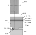
このアライメントマークに関して、特許文献1にて提案されており、その一例についての断面図を図9に示す。 This alignment mark is proposed in Patent Document 1, and a cross-sectional view of an example thereof is shown in FIG.
特許文献1のアライメントマークAMは、図9に示す通り、シリコンを貫通した形状に絶縁特性のある材料が埋め込まれた絶縁体部AILD1(上部の絶縁体部AILD1)と
その下部の絶縁体部AILD2(下部の絶縁体部AILD2)から構成される。これらの絶縁体部AILD1,AILD2の幅の寸法は図示している通り、下部の絶縁体部AILD2の方が大きい。これにより、下部の絶縁体部AILD2が保護膜として機能し、ポリシリコンの堆積による短絡(電気的なショート)の防止や、シリコン酸化膜が剥がれてしまった場合の、ウエハ汚染や装置汚染の防止を可能としている。
As shown in FIG. 9, the alignment mark AM of Patent Document 1 includes an insulator part AILD1 (an upper insulator part AILD1) in which a material with insulating properties is embedded in a shape that penetrates silicon, and an insulator part AILD2 below it. (lower insulator portion AILD2). As shown in the figure, the width of these insulator portions AILD1 and AILD2 is larger in the lower insulator portion AILD2. As a result, the lower insulator portion AILD2 functions as a protective film, preventing short circuits (electrical short circuits) due to polysilicon deposition, and preventing wafer contamination and equipment contamination when the silicon oxide film is peeled off. is possible.
また、BSI型のセンサでは、基板表面側の配線構造に形成された電極パッドPADを、
基板裏面側に導出するために、基板裏面側から電極パッド形成領域が臨む開口部を形成する必要がある。開口部により電極パッド形成領域を露出することで、外部配線となるボンディングワイヤ等を形成して電極パッドPADを基板裏面側に導出できる。電極パッドPADにワイヤーボンディングする際や検査工程において電極パッドPADにプローブする際に、誤って側壁に接触した場合でもリークやダメージを抑制するために、このボンディングワイヤと半導体部とを絶縁する必要がある。そのため開口部に周囲に二層の絶縁体部ILD1,ILD2を配置する。この二層の絶縁体部の構成は前述のアライメントマークAM(AILD1,AILD2)と同じく、下部の絶縁体部ILD2が上部の絶縁体部ILD1を保護する構成となっている。
In addition, in the BSI type sensor, the electrode pad PAD formed in the wiring structure on the surface side of the substrate is
In order to lead out to the back side of the substrate, it is necessary to form an opening through which the electrode pad formation region faces from the back side of the substrate. By exposing the electrode pad formation region through the opening, bonding wires and the like serving as external wiring can be formed to lead out the electrode pad PAD to the back side of the substrate. When wire bonding to the electrode pad PAD or when probing the electrode pad PAD during the inspection process, it is necessary to insulate the bonding wire from the semiconductor part in order to prevent leakage and damage even if the sidewall is accidentally contacted. be. Therefore, two-layer insulator portions ILD1 and ILD2 are arranged around the opening. The structure of this two-layer insulator section is similar to the aforementioned alignment mark AM (AILD1, AILD2), in which the lower insulator section ILD2 protects the upper insulator section ILD1.
また、特許文献1では、アライメントマークと電極パッド開口部周囲の二層の絶縁体部を同時に形成するとしている。 Further, in Patent Document 1, an alignment mark and a two-layer insulator portion around an electrode pad opening are formed at the same time.
特許文献1に示される縦構造のアライメントマークを使用すると、固体撮像装置の製造歩留まりや固体撮像装置の品質が低下してしまうことが我々の検討により判明した。 Our studies have revealed that the use of the vertically structured alignment mark disclosed in Patent Document 1 results in a decrease in the manufacturing yield of the solid-state imaging device and the quality of the solid-state imaging device.
そこで、本発明は、従来よりも光電変換装置の製造歩留まりや光電変換装置の品質を向上するうえで有利な技術を提供する。 Therefore, the present invention provides a technology that is advantageous in improving the manufacturing yield of photoelectric conversion devices and the quality of photoelectric conversion devices compared to the conventional techniques.
本発明の一態様に係る光電変換装置は、
光電変換部を有し、表面および裏面を有する半導体層と、
前記半導体層の前記表面の上に配置された、絶縁膜を含む配線構造と、
アライメントマークと、
を備える光電変換装置であって、
前記アライメントマークは、
前記半導体層に設けられた溝の内に配置された第一の絶縁体部と、
前記第一の絶縁体部と前記絶縁膜との間に配置された第二の絶縁体部と、
を備え、
前記第一の絶縁体部の幅の最大値が、前記第二の絶縁体部の幅の最大値よりも大きく、
上面透視したときに、前記第一の絶縁体部の外縁が前記第二の絶縁体部の外縁を内包する、
ことを特徴とする。
本発明の他の一態様に係る光電変換装置は、
光電変換部を有し、表面および裏面を有する半導体層と、
前記半導体層の前記表面の上に配置された、絶縁膜を含む配線構造と、
アライメントマークと、
を備える光電変換装置であって、
前記アライメントマークは、
前記半導体層に設けられた溝の内に配置された第一の絶縁体部と、
前記第一の絶縁体部と前記絶縁膜との間に配置された第二の絶縁体部と、
を備え、
前記第一の絶縁体部および前記第二の絶縁体部は、平面視において矩形形状であり、
上面透視したときに、前記第二の絶縁体部の長手方向に延びる端部の両方が、前記第一の絶縁体部の長手方向に延びる2つの端部の間に位置する、
ことを特徴とする。
A photoelectric conversion device according to one embodiment of the present invention includes:
a semiconductor layer having a photoelectric conversion portion and having a front surface and a back surface;
a wiring structure including an insulating film disposed on the surface of the semiconductor layer;
alignment mark and
A photoelectric conversion device comprising:
The alignment mark is
a first insulator portion disposed within a groove provided in the semiconductor layer;
a second insulator section disposed between the first insulator section and the insulating film;
Equipped with
The maximum width of the first insulator portion is larger than the maximum width of the second insulator portion,
When viewed from above, the outer edge of the first insulator section includes the outer edge of the second insulator section;
It is characterized by
A photoelectric conversion device according to another aspect of the present invention,
a semiconductor layer having a photoelectric conversion portion and having a front surface and a back surface;
a wiring structure including an insulating film disposed on the surface of the semiconductor layer;
alignment mark and
A photoelectric conversion device comprising:
The alignment mark is
a first insulator portion disposed within a groove provided in the semiconductor layer;
a second insulator section disposed between the first insulator section and the insulating film;
Equipped with
The first insulator part and the second insulator part have a rectangular shape in plan view,
When viewed from above, both longitudinally extending ends of the second insulator are located between two longitudinally extending ends of the first insulator.
It is characterized by
本発明によれば、光電変換装置の製造歩留まりや光電変換装置の品質を向上するうえで有利な技術が提供される。 According to the present invention, a technology advantageous for improving the manufacturing yield of photoelectric conversion devices and the quality of photoelectric conversion devices is provided.
<従来のアライメントマークの問題点>
特許文献1に示される縦構造のアライメントマークを使用すると、アライメント精度が劣化してしまうことが我々の検討により判明した。
<Problems with conventional alignment marks>
Our studies have revealed that when the vertically structured alignment mark shown in Patent Document 1 is used, alignment accuracy deteriorates.
精度劣化の理由は、アライメントマークAMを構成している二層の絶縁膜AILD1,AILD2のうち、下部の絶縁体部AILD2もアライメント計測時に観察できてしまうためである。したがって、上部の絶縁体部AILD1と下部の絶縁体部AILD2とのアライメント状態に誤差があり二層の相対関係がズレていると、その影響を受けてアライメ
ントマークAMの位置を正しく検出できず、アライメント精度が劣化する。
The reason for the deterioration in accuracy is that the lower insulator portion AILD2 of the two-layer insulating films AILD1 and AILD2 constituting the alignment mark AM can also be observed during alignment measurement. Therefore, if there is an error in the alignment between the upper insulator part AILD1 and the lower insulator part AILD2 and the relative relationship between the two layers is out of alignment, the position of the alignment mark AM cannot be detected correctly due to the influence. Alignment accuracy deteriorates.
上記の検討に用いたアライメントマークAMを図10に示す。アライメント検出系(図3参照)は画像処理によりアライメントマークの検出を行う。具体的には、波長550nm~700nmの光でウエハ上のアライメントマーク(図2に詳細図を示す)を照明し、ウエハから反射する光をCCDカメラ上に光学倍率100倍以上で結像させ、アライメントマークの光学像を光電変換して画像信号を得る。そして、画像信号に画像処理を施すことでアライメントマークの位置をサブナノメートル精度で検出する。 FIG. 10 shows the alignment mark AM used in the above study. The alignment detection system (see FIG. 3) detects alignment marks by image processing. Specifically, the alignment mark on the wafer (detailed diagram is shown in Figure 2) is illuminated with light with a wavelength of 550 nm to 700 nm, and the light reflected from the wafer is imaged on a CCD camera at an optical magnification of 100 times or more. The optical image of the alignment mark is photoelectrically converted to obtain an image signal. Then, by performing image processing on the image signal, the position of the alignment mark is detected with sub-nanometer precision.
図10は、検討に用いたアライメントマークAMの上面図1010と、AA断面における断面図1020を示す。図10に示す構造は、BSIの構造を模した縦構造であり、シリ
コン酸化膜SiO (2500Å)の高さのパターン1021を、3μmの厚さのシリコン1022
を通して観察できることが判る。この像のコントラストが十分高いものであれば、特許文献1で提案する様に貫通した形状のアライメントマークを使う必要がない。しかしながら、図10の様にパターン1021の観察はできるが、コントラストが低くサブナノメートルの計測ができる信号レベルではない。
FIG. 10 shows a
It turns out that it can be observed through. If the contrast of this image is sufficiently high, there is no need to use a penetrating alignment mark as proposed in Patent Document 1. However, although the
図9に示したアライメントマークを使う場合には、低コントラストの像が、アライメント精度の劣化の原因となる。この説明をするために、アライメントマークをどう形成するかを、図11A~図11Eを使って説明する。 When using the alignment mark shown in FIG. 9, a low contrast image causes deterioration in alignment accuracy. To explain this, how to form alignment marks will be explained using FIGS. 11A to 11E.
まず、図11Aに示すように、シリコンウエハ111上にトレンチ(溝)をリソグラフィの露光・現像・エッチングで形成し、その溝にシリコン窒化膜(SiN)112を埋め込
む。このトレンチが、後の「上部の絶縁体部AILD1」となる(ただし、図11A~図11Cは基板の上下反転前なのでシリコン窒化膜(SiN)112は下部にある)。
First, as shown in FIG. 11A, a trench is formed on a
次に、図11Bに示すように、図11Aで同時に形成したアライメントマーク(不図示)を使って、「上部の絶縁体部AILD1」上に「下部の絶縁体部AILD2」となるパターンを、リソグラフィのアライメント・露光・現像・エッチングで形成する。図11Cは、図11Bで形成したパターンに絶縁材であるシリコン酸化膜(SiO)113を埋め込
み、「下部の絶縁体部AILD2」が形成された状態を示す図である。
Next, as shown in FIG. 11B, using the alignment marks (not shown) formed at the same time in FIG. Formed by alignment, exposure, development, and etching. FIG. 11C is a diagram showing a state in which a silicon oxide film (SiO) 113, which is an insulating material, is embedded in the pattern formed in FIG. 11B to form a "lower insulator portion AILD2."
図11Dは、図11Cに示す基板を上下反転させた状態を示す図である。なお、図11A~図11Dにおいて、シリコン(Si)の厚さは強調して示されている。最後に、図11Eに示すように、図11Dの基板に対して、BSIプロセスで行う研削を行い、シリコン(Si)の厚さを3μmとする。図11Dに示す状態は、図10で示した縦構造と同一のものである。 FIG. 11D is a diagram showing a state in which the substrate shown in FIG. 11C is turned upside down. Note that in FIGS. 11A to 11D, the thickness of silicon (Si) is emphasized. Finally, as shown in FIG. 11E, the substrate shown in FIG. 11D is ground using a BSI process to reduce the thickness of silicon (Si) to 3 μm. The state shown in FIG. 11D is the same as the vertical structure shown in FIG.
上記の手順で作成されるアライメントマークにおいて、「上部の絶縁体部AILD1」と「下部の絶縁体部AILD2」の中心は同じに配置されるべきだが、実際にはアライメント精度(許容範囲)内で位置ずれが生じる。このような状態を「位置ずれが生じている」と呼ぶことにする。また、位置ずれ量がΔである場合には、「位置ずれ量Δの位置ずれが生じている」あるいは「Δの位置ずれが生じている」などと呼ぶことにする。 In the alignment mark created by the above procedure, the centers of "upper insulator part AILD1" and "lower insulator part AILD2" should be placed at the same center, but in reality, the centers are within the alignment accuracy (tolerable range). Misalignment occurs. Such a state will be referred to as "positional deviation has occurred." Furthermore, when the amount of positional deviation is Δ, it will be referred to as “a positional deviation of the amount of positional deviation Δ has occurred” or “a positional deviation of Δ has occurred”.
図11Eで示したアライメントマークに位置ずれが生じるとどのように観測されるかを、図12A~図12Cを参照して説明する。図12Aは、位置ずれが生じていない理想的な状態121と、状態121をアライメント検出系によって計測したときに検出される信号122を示す。信号122は歪の無い対称なものとなり、アライメント誤差は生じない。
How it is observed when a positional shift occurs in the alignment mark shown in FIG. 11E will be described with reference to FIGS. 12A to 12C. FIG. 12A shows an
一方、図12Bでは+Δの位置ずれが生じている状態123と、状態123を計測したときに検出される信号124を示す。なおここでは、「下部の絶縁体部AILD2」が「上部の絶縁体部AILD1」に対して左にずれている場合の位置ずれ量を、正と定義している。+Δの位置ずれに起因して、信号124に歪が発生して非対称となり、アライメント誤差が発生する。信号124に歪みがあると、上部の絶縁体部AILD1の中心からずれた位置がアライメントマークの位置として検出され、アライメント誤差が生じる。図12Bの例では、上部の絶縁体部AILD1の中心から左(正方向)にずれた位置がアライメントマークの位置として検出されることになる。
On the other hand, FIG. 12B shows a
図12Cは、図12Bとは逆の方向にずれた状態、すなわち-Δの位置ずれが生じている状態125と、状態125を計測したときに検出される信号126を示す。図12Bに示す場合と同様に、信号126に歪が発生して非対称となりアライメント誤差が発生する。ただし、アライメント誤差は、図12Bの場合とは逆方向に発生する。
FIG. 12C shows a
このように、上部の絶縁体部AILD1と下部の絶縁体部AILD2のあいだの位置ずれにより発生するアライメントマークの検出位置の誤差が、アライメント精度を劣化させる問題となる。 As described above, the error in the detection position of the alignment mark caused by the positional deviation between the upper insulator portion AILD1 and the lower insulator portion AILD2 poses a problem that deteriorates the alignment accuracy.
またBSI型のセンサでは、重ね合わせ精度が劣化する問題が知られている。重ね合わせ
精度の劣化は、前述のBSI型のセンサを形成するプロセス中の、一つのウエハ基板を反転
させて別のウエハ基板に貼り付ける工程で生じるウエハ基板全体の歪に起因する。
Additionally, BSI type sensors are known to have a problem in which overlay accuracy deteriorates. The deterioration in overlay accuracy is caused by the distortion of the entire wafer substrate that occurs during the step of inverting one wafer substrate and attaching it to another wafer substrate during the process of forming the aforementioned BSI type sensor.
ウエハ基板の貼り付けは、銅と銅を貼り合わせるハイブリッド・ボンディングという方法が一般に使用されている。図9は、上側のボンディング用マークUHBと下側のボンディング用マークLHBを使って、二枚のウエハ基板を貼り合わされた状態を示している。この貼り合わせを行う時にウエハ基板全面で均一に行うことができず、ある特定の部分から貼り合わされることでウエハ基板の平面方向に歪を発生させる。レーザー干渉計を使うことでサブナノメーター制御するウエハステージを使った半導体露光装置で各ショットを露光した時に形成した各ショットの格子形状を歪ませてしまい、重ね合わせ精度を劣化させてしまう。 For bonding wafer substrates, a method called hybrid bonding, in which copper and copper are bonded together, is generally used. FIG. 9 shows a state in which two wafer substrates are bonded together using an upper bonding mark UHB and a lower bonding mark LHB. When this bonding is performed, it cannot be performed uniformly over the entire surface of the wafer substrate, and bonding starts from a certain portion, causing distortion in the plane direction of the wafer substrate. By using a laser interferometer, the lattice shape of each shot formed when each shot is exposed by a semiconductor exposure system using a wafer stage controlled by subnanometers is distorted, which deteriorates overlay accuracy.
全ショットを露光装置で計測することや重ね合わせ検査装置を使った複数の計測結果を反映した非線形補正も提案され使用されているが、著しいスループットの低下を発生させている。 Measurement of all shots with an exposure device and nonlinear correction that reflects multiple measurement results using an overlay inspection device have also been proposed and used, but this causes a significant decrease in throughput.
そのため、BSI型のセンサでは、重ね合わせ精度の向上が今後の微細化と高生産性には
重要な事項である。
Therefore, for BSI type sensors, improving overlay accuracy is important for future miniaturization and high productivity.
<実施形態1>
本実施形態では、ウエハアライメント用のマークを形成する「下部の絶縁体部AILD2」と「上部の絶縁体部AILD1」の間に位置ずれが生じている場合でも、アライメント精度を劣化させないアライメントマークを提案する。本実施形態で提案するアライメントマークを用いることで、BSI型の光電変換装置を、高精度かつ効率的に製造できるよう
になる。
<Embodiment 1>
In this embodiment, even if there is a positional shift between the "lower insulator part AILD2" and the "upper insulator part AILD1" that form the mark for wafer alignment, an alignment mark that does not deteriorate alignment accuracy is created. suggest. By using the alignment mark proposed in this embodiment, it becomes possible to manufacture a BSI type photoelectric conversion device with high precision and efficiency.
[構成]
図1は、本実施形態の光電変換装置の概略構成図を示す。図1に示すように、本実施形態の光電変換装置は、画素領域PiAの周辺領域に、製造時において位置決めに用いられるアライメントマークAMと、外部配線との接続に用いられる電極パッドPADが形成された電極パッド形成領域PaAを有して構成される。
[composition]
FIG. 1 shows a schematic configuration diagram of a photoelectric conversion device of this embodiment. As shown in FIG. 1, in the photoelectric conversion device of this embodiment, an alignment mark AM used for positioning during manufacturing and an electrode pad PAD used for connection with external wiring are formed in the peripheral area of the pixel area PiA. The electrode pad forming area PaA is configured to have an electrode pad formation area PaA.
裏面照射型の光電変換装置1は、光電変換を行うフォトダイオードPDが形成された半導体層(シリコン層)11と、半導体層の表面側に形成された配線構造12と、半導体層の裏面側に形成されたカラーフィルタCFやマイクロレンズMLから構成される。また、配線構造12の半導体層11に接する面とは反対側の面には、支持基板13が形成されている。
A back-illuminated photoelectric conversion device 1 includes a semiconductor layer (silicon layer) 11 on which a photodiode PD that performs photoelectric conversion is formed, a
半導体層11の画素領域PiAには、受光センサ部となるフォトダイオードPDが形成され、受光センサ部は受光した光の光量に応じた信号電荷を生成する光電変換を行う。画素領域PiAには、図示はしていないが、画素を駆動する画素トランジスタが各画素に隣接して形成されている。
A photodiode PD serving as a light-receiving sensor section is formed in the pixel region PiA of the
配線構造12は、アルミニウムまたは銅からなる配線および層間絶縁膜を含み、配線が層間絶縁膜を介して複数層(図1では2層)積層された構成を有する。各配線間または配線と画素トランジスタの間は、図示しないコンタクト部によって電気的に接続されている。また、周辺領域では、アルミニウムからなる配線の一部により、電極パッドPADが形成されている。
The
カラーフィルタCFは半導体層11の光照射側となる裏面側の各画素に対応する領域に形成されており、例えば、赤色(R)、緑色(G)、青色(B)の色素を含む有機材料で構成されている。マイクロレンズMLは、各画素に対応してカラーフィルタCF上部に有機材料によって形成されている。マイクロレンズMLは、入射した光が対応する画素のフォトダイオードPDに効率良く入射するように集光する。
The color filter CF is formed in a region corresponding to each pixel on the back side of the
アライメントマークAMは、半導体層11のスクライブ領域SAに形成されており、半導体層内に上部の絶縁体部ATILD1(第一の絶縁体部)と下部の絶縁体部AILD2(第二の絶縁体部)が積層されている。ここでは、フォトダイオードPDが受光する光の入射側を上側としているので、上部の絶縁体部ATILD1は、下部の絶縁体部AILD2に対して、受光する光の側に配置される。上部の絶縁体部ATILD1は、半導体層11の下側において、下部の絶縁体部AILD2と接続している。下部の絶縁体部AILD2は、上部の絶縁体部ATILD1を被覆しており、保護膜として機能する。アライメントマークAM(上部の絶縁体部ATILD1)は、半導体層11の裏面側においてカラーフィルタCFやマイクロレンズMLを形成する際の位置決めに用いられる。
The alignment mark AM is formed in the scribe area SA of the
本実施形態におけるアライメントマークは、平面視において矩形形状である(図2参照)。ここで、図4Aにも示すように、上部の絶縁体部ATILD1は、光が入射する上部側ほど幅が大きいテーパー形状を有する。なお、本開示におけるアライメントマークの「幅」は、平面視における矩形の短手方向(図2にしめすx方向)の寸法を意味する。なお、上部の絶縁体部ATILD1の長手方向の寸法も上部側ほど長くてもよい。下部の絶縁体部AILD2の形状は、図9と同様であり、高さによらずに略一定の幅を有する。スクライブ領域SAには、図2に示すように、アライメントマークが複数併置される。横方向の位置を検知するためには、縦長のアライメントマークが横方向に複数併置される。 The alignment mark in this embodiment has a rectangular shape in plan view (see FIG. 2). Here, as also shown in FIG. 4A, the upper insulator portion ATILD1 has a tapered shape whose width increases toward the upper side where light enters. Note that the "width" of the alignment mark in the present disclosure means the dimension in the transverse direction (x direction shown in FIG. 2) of a rectangle in plan view. Note that the longitudinal dimension of the upper insulator portion ATILD1 may also be longer toward the upper side. The shape of the lower insulator portion AILD2 is similar to that shown in FIG. 9, and has a substantially constant width regardless of the height. As shown in FIG. 2, a plurality of alignment marks are placed side by side in the scribe area SA. In order to detect the position in the horizontal direction, a plurality of vertically long alignment marks are placed side by side in the horizontal direction.
なお、アライメントマークはスクライブ領域SA以外、すなわちチップ内に配置されてもよい。 Note that the alignment mark may be placed outside the scribe area SA, that is, within the chip.
本実施形態において、上部の絶縁体部ATILD1の上端における幅Wud(言い換えると幅の最大値)は、下部の絶縁体部AILD2の幅W2よりも、絶縁体部ATILD1,AILD2を形成するときのアライメント誤差(許容誤差)Δcの二倍以上である。言い換えると上部の絶縁体部ATILD1の上端における幅Wudは、下部の絶縁体部AI
LD2の幅と、アライメント誤差Δcの二倍との和以上(Wud≧W2+2×Δc)である。このような構成なので、2つの絶縁体部の位置ずれ量Δがアライメント誤差Δc以下である限り、アライメントマークを上面透視したときに、下部の絶縁体部AILD2の幅は、上部の絶縁体部ATILD1の幅の範囲内に収まる。すなわち、アライメントマークを上面透視したときに、下部の絶縁体部AILD2の幅方向の端部E2a,E2bの両方が、上部の絶縁体部ATILD1の端部E1a,E1bの間に位置する。
In this embodiment, the width Wud (in other words, the maximum width) at the upper end of the upper insulator part ATILD1 is greater than the width W2 of the lower insulator part AILD2 when forming the insulator parts ATILD1 and AILD2. It is more than twice the error (tolerable error) Δ c . In other words, the width Wud at the upper end of the upper insulator portion ATILD1 is equal to the width Wud at the upper end of the upper insulator portion ATILD1.
It is greater than or equal to the sum of the width of LD2 and twice the alignment error Δ c (Wud≧W2+2×Δ c ). With such a configuration, as long as the amount of positional deviation Δ between the two insulator parts is less than or equal to the alignment error Δ c , the width of the lower insulator part AILD2 is equal to the width of the upper insulator part when the alignment mark is seen through from above. It falls within the width of ATILD1. That is, when the alignment mark is viewed from above, both ends E2a and E2b in the width direction of the lower insulator part AILD2 are located between the ends E1a and E1b of the upper insulator part ATILD1.
また、上部の絶縁体部ATILD1の下端(下部の絶縁体部AILD2と接続する部分)の幅は、下部の絶縁体部AILD2の幅よりも小さい。これにより、下部の絶縁体部AILD2が保護膜として機能する。 Further, the width of the lower end of the upper insulator portion ATILD1 (the portion connected to the lower insulator portion AILD2) is smaller than the width of the lower insulator portion AILD2. Thereby, the lower insulator portion AILD2 functions as a protective film.
なお、上部の絶縁体部ATILD1の縦方向の寸法も、光が入射する上部側ほど長くてもよい。この場合、アライメントマークを上面から見たとき、すなわち、シリコン層の表面と垂直な方向からの上面透視において、下部の絶縁体部AILD2は、上部の絶縁体部ATILD1の内部に位置する。 Note that the vertical dimension of the upper insulator portion ATILD1 may also be longer toward the upper side where light is incident. In this case, when the alignment mark is viewed from above, that is, when viewed through the top from a direction perpendicular to the surface of the silicon layer, the lower insulator portion AILD2 is located inside the upper insulator portion ATILD1.
また、電極パッド配置領域PaA内の電極パッドPADの周囲に配置される絶縁体部も、アライメントマークと同様に二層構造であり、上部の絶縁体部TILD1は光が入射する上部側の幅が大きいテーパー形状を有する。下部の絶縁体部ILD2の形状は、図9と同様で有り、高さによらずに略一定の幅を有する。半導体基板は、電極パッドPADを基板裏面側に導出するために、開口部を設けて電極パッドPADを露出する。絶縁体部TILD1,ILD2が設けられることで、ワイヤーボンディングする際や検査工程などにおいて誤って側壁に接触した場合でもリークやダメージを抑制できる。また、下部の絶縁体部ILD2の幅が小さいので、配置領域PaAの近傍で生じる、応力を低減できる。そのため、光電変換装置の製造歩留まりや光電変換装置の品質を向上することができる。 In addition, the insulator section arranged around the electrode pad PAD in the electrode pad arrangement area PaA also has a two-layer structure like the alignment mark, and the upper insulator section TILD1 has a width on the upper side where light enters. It has a large taper shape. The shape of the lower insulator portion ILD2 is similar to that shown in FIG. 9, and has a substantially constant width regardless of the height. The semiconductor substrate is provided with an opening to expose the electrode pad PAD in order to lead out the electrode pad PAD to the back side of the substrate. By providing the insulator parts TILD1 and ILD2, leakage and damage can be suppressed even if the sidewall is accidentally contacted during wire bonding or an inspection process. Furthermore, since the width of the lower insulator portion ILD2 is small, stress generated in the vicinity of the arrangement region PaA can be reduced. Therefore, the manufacturing yield of the photoelectric conversion device and the quality of the photoelectric conversion device can be improved.
[効果]
図4A~図4Cを参照して、アライメントマークを構成する上部の絶縁体部ATILD1と下部の絶縁体部AILD2のあいだに位置ずれがあっても、カラーフィルタやマイクロレンズ形成時のアライメント精度の劣化が生じないことを説明する。
[effect]
Referring to FIGS. 4A to 4C, even if there is a positional shift between the upper insulator part ATILD1 and the lower insulator part AILD2 that constitute the alignment mark, the alignment accuracy deteriorates when forming color filters and microlenses. Explain that this will not occur.
なお、アライメントマークの検出に用いられるアライメント検出系30の構成を図3に示す。図3に示したアライメント検出系30の計測方法は画像処理である。光源31から波長550nm~700nmの光が発せられ、反射板32、ビームスプリッタ33、レンズ34を介して、ウエハ上のアライメントマークAMを照明する。アライメントマークAMからの回折光は、レンズ34,ビームスプリッタ33,レンズ35,36により100倍程度の結像倍率で拡大されて、CCDカメラ37に結像される。CCDカメラ37は、アライメントマークAMの光学像を光電変換した撮像信号を信号処理部に送出し、信号処理部が撮像信号に基づいてアライメントマークの位置情報を算出する。
Note that FIG. 3 shows the configuration of an
図4A~図4Cは、図12A~図12Cと同様に、位置ずれが生じていない場合、+Δの位置ずれが生じている場合、-Δの位置ずれが生じている場合の、アライメントマークの状態および検出されるアライメント信号をそれぞれ示す。 Similar to FIGS. 12A to 12C, FIGS. 4A to 4C show the alignment mark states when no positional deviation occurs, when a +Δ positional deviation occurs, and when a −Δ positional deviation occurs. and detected alignment signals, respectively.
図4Aは、図12Aと同じように、位置ずれが発生していない、理想的に合った状態41と、検出されるアライメント信号42を示す。アライメント検出系30により検出される検出信号42は歪の無い対称なものとなり、アライメント誤差は生じない。
Similar to FIG. 12A, FIG. 4A shows an ideally matched
一方、図4Bは、図12Bと同じように、+Δの位置ずれが生じている状態43と、状態43を計測したときに検出される信号44を示す。なおここでは、「下部の絶縁体部A
ILD2」が「上部の絶縁体部ATILD1」に対して左にずれている場合の位置ずれ量を、正と定義している。
On the other hand, like FIG. 12B, FIG. 4B shows a
The amount of positional shift when "ILD2" is shifted to the left with respect to "upper insulator portion ATILD1" is defined as positive.
上述したように、テーパー形状の絶縁体部ATILD1の上部の幅Wudの大きさは、下部の絶縁体部AILD2の幅W2と二倍のΔ(<Δc)より大きな寸法である。したがって、アライメント検出系により上部からアライメントマークを観察する際に、下部の絶縁体部AILD2は、絶縁体部ATILD1の上部の陰になり観察されない。この結果、検出されるアライメント信号(の少なくとも両端)の部分は非対称にならない。非対称にならないことはアライメント精度が劣化しないことになり、上述した課題を解決できる。 As described above, the width Wud of the upper part of the tapered insulator part ATILD1 is larger than Δ (<Δ c ), which is twice the width W2 of the lower insulator part AILD2. Therefore, when observing the alignment mark from above using the alignment detection system, the lower insulator part AILD2 is hidden by the upper part of the insulator part ATILD1 and cannot be observed. As a result, the portions of (at least both ends of) the detected alignment signal are not asymmetrical. The absence of asymmetry means that alignment accuracy does not deteriorate, and the above-mentioned problem can be solved.
材質の透過率や吸収率、あるいは検出に使用する光の波長によっては、「下部の絶縁体部AILD2」の影響が、(量としては僅かであるものの)アライメント信号に現れることは考えられる。しかしながら、上部の絶縁体部ATILD1をテーパー形状とすることで、影響が現れる位置を、図4B中の信号位置Sibの部分の様に、アライメント信号の両
端とならない様にできる。信号処理で実際に使用する部分の処理ウインドウはエッジ部分、すなわちアライメント信号の両端部であるため、信号位置Sibの部分は、アライメント
マークの位置検出に影響を与えない。したがって、上部と下部の絶縁体部の間に位置ずれが生じていても、アライメントマークの位置を正確に検出できる。
Depending on the transmittance or absorption rate of the material or the wavelength of the light used for detection, it is conceivable that the influence of the "lower insulator portion AILD2" will appear on the alignment signal (although the amount is small). However, by making the upper insulator portion ATILD1 tapered, the position where the influence appears can be prevented from being at both ends of the alignment signal, as in the signal position Sib in FIG. 4B. Since the processing window of the portion actually used in signal processing is the edge portion, that is, both ends of the alignment signal, the portion of the signal position Sib does not affect the position detection of the alignment mark. Therefore, even if there is a positional shift between the upper and lower insulator parts, the position of the alignment mark can be detected accurately.
図4Cは、図4Bとは逆方向の位置ずれが生じている状態45と、状態45を計測したときに検出される信号46を示す。図4Cの場合も、図4Bと同様の理由によりアライメント精度が劣化しないので、詳細な説明は省略する。
FIG. 4C shows a
図5A,図5Bを参照して、本実施形態の効果をさらに説明する。図5Aおよび図5Bはそれぞれ、従来技術および本実施形態において位置ずれが生じているアライメントマーク(図12Bおよび図4B)を、半導体露光装置のアライメント検出系で観察した場合のアライメントマークの一部を拡大した図である。 The effects of this embodiment will be further described with reference to FIGS. 5A and 5B. FIGS. 5A and 5B show a part of the alignment mark when the alignment mark (FIG. 12B and FIG. 4B) in which positional deviation occurs in the conventional technology and the present embodiment is observed using an alignment detection system of a semiconductor exposure apparatus, respectively. This is an enlarged view.
図5Aは、従来技術(特許文献1)で提案するアライメントマークの一部を拡大したものである。位置ずれが生じていることにより、下部の絶縁体部AILD2のズレの影響が左側に現れている。これにより、上部の絶縁体部AILD1の端部を誤検出し、アライメントマーク(上部の絶縁体部AILD1)の検出位置に誤差が生じる。 FIG. 5A is an enlarged view of a part of the alignment mark proposed in the prior art (Patent Document 1). Due to the positional shift, the influence of the shift of the lower insulator portion AILD2 appears on the left side. As a result, the end of the upper insulator portion AILD1 is erroneously detected, and an error occurs in the detected position of the alignment mark (upper insulator portion AILD1).
一方、図5Bに示す本実施形態のアライメントマークの一部を拡大したものである。位置ずれによる下部の絶縁体部の影響を受けたとしても、その影響を受ける位置を、マーク端部とならない構成とすることで、アライメントマークの位置を正確に検出できる。つまり、アライメント精度劣化の発生を防ぐことができる。 On the other hand, it is an enlarged view of a part of the alignment mark of this embodiment shown in FIG. 5B. Even if the lower insulator section is affected by misalignment, the position of the alignment mark can be accurately detected by configuring the structure so that the affected position does not become the end of the mark. In other words, it is possible to prevent deterioration in alignment accuracy.
このように、「下部の絶縁体部AILD2」は保護膜としては機能するが、アライメントマークとしては機能しない。 In this way, the "lower insulator portion AILD2" functions as a protective film, but does not function as an alignment mark.
[製造方法]
図6A~図6Fを参照して、本実施形態におけるアライメントマークを構成する、テーパー形状の絶縁体部ATILD1の形成する工程を説明する。
[Production method]
With reference to FIGS. 6A to 6F, the process of forming the tapered insulator portion ATILD1, which constitutes the alignment mark in this embodiment, will be described.
まず、図6Aに示すように、シリコンウエハ601上に逆テーパーの形状のトレンチ602をリソグラフィの露光・現像・エッチングで形成する。なお、図6A~図6Cは、基板の上下反転前を示しており、最終的には図面下側が「上部」となる。
First, as shown in FIG. 6A, a
使用するドライエッチング装置は、いずれのドライエッチング装置を用いても実施する
ことができ、特に制限されるものではない。そのようなドライエッチング装置として、ICP型エッチング装置、マグネトロンRIE型エッチング装置、2周波平行平板型エッチング装置等を例示することができる。
The dry etching apparatus to be used is not particularly limited, and any dry etching apparatus can be used. Examples of such a dry etching device include an ICP type etching device, a magnetron RIE type etching device, a two-frequency parallel plate type etching device, and the like.
例えば、以下のエッチング条件を用いて二酸化シリコンSiO2をエッチングマスクとしてシリコン601をエッチングすることで図6Aに示した逆テーパーの形状のトレンチ1002を形成することが出来る。
・プロセスガスの圧力:10~200mTorr
・上部RFパワー:100~2000W
・下部RFパワー:100~2000W
・HBrガスの流量:20~300sccm
・NF3ガスの流量:0~200sccm
・O2ガスの流量:0~50sccm
For example, by etching the
・Process gas pressure: 10-200mTorr
・Upper RF power: 100-2000W
・Lower RF power: 100-2000W
・HBr gas flow rate: 20 to 300 sccm
・NF3 gas flow rate: 0 to 200 sccm
・O2 gas flow rate: 0 to 50 sccm
次に、図6Bに示すように、トレンチ602にシリコン窒化膜(SiN)603を埋め込
む。このシリコン窒化膜603が、最終的に上部の絶縁体部ATILD1となる。
Next, as shown in FIG. 6B, the
次に、図6Cに示すように、シリコン窒化膜603(上部の絶縁体部ATILD1)の上に、「下部の絶縁体部AILD2」となるパターン604を、リソグラフィのアライメント・露光・現像・エッチングで形成する。この工程でのアライメントには、図6Aにおいてトレンチ602と同時に形成したアライメントマーク(不図示)を使う。
Next, as shown in FIG. 6C, a
次に、図6Dに示すように、図6Cにおいて形成したパターン604に絶縁材であるシリコン酸化膜(SiO)605を埋め込む。シリコン酸化膜605が、最終的に下部の絶縁
体部AILD2となる。
Next, as shown in FIG. 6D, a silicon oxide film (SiO) 605, which is an insulating material, is embedded in the
次に、図6Eに示すように、図6Dに示す基板の上下を反転する。なお、図6A~図6Eにおいて、シリコン(Si)601の厚さは強調して示されている。 Next, as shown in FIG. 6E, the substrate shown in FIG. 6D is turned upside down. Note that in FIGS. 6A to 6E, the thickness of silicon (Si) 601 is emphasized.
次に、図6Fに示すように、図6Eの基板に対して、BSIプロセスで行う研削を行い、
シリコン(Si)601の厚さを3μmとする。
Next, as shown in FIG. 6F, the substrate in FIG. 6E is subjected to grinding using the BSI process.
The thickness of silicon (Si) 601 is 3 μm.
この様にして、BSIプロセスでカラーフィルタ及びにマイクロレンズを形成するリソグ
ラフィに使用するアライメントマークを形成できる。
In this way, alignment marks used in lithography for forming color filters and microlenses in the BSI process can be formed.
なお、電極パッドPADの周囲の絶縁体部TILD1,ILD2も、上記のプロセスによってアライメントマーク同時に形成される。 Note that the insulator portions TILD1 and ILD2 around the electrode pad PAD are also formed at the same time as the alignment mark by the above process.
[本実施形態の有利な効果]
本実施形態によれば、撮像領域の周辺のテーパー形状の溝に埋め込まれた絶縁体部を、位置合わせマークとして利用して、受光センサ部(フォトダイオードPD等)とカラーフィルタCFやマイクロレンズMLとの位置合わせを高精度に行うことが可能になる。従って、本実施形態により、BSI構造の光電変換装置を高精度かつ効率的に生産可能となる。
そして、光電変換装置の製造歩留まりや光電変換装置の品質を向上することができる。BSI構造の光電変換装置は、斜め入射光の実効開口率100%を達成可能であり、感度を大
幅に向上し、またシェーディングレスを実現可能である。
[Advantageous effects of this embodiment]
According to this embodiment, the insulator part embedded in the tapered groove around the imaging area is used as a positioning mark to align the light receiving sensor part (photodiode PD, etc.) with the color filter CF and the microlens ML. This makes it possible to perform highly accurate positioning. Therefore, according to this embodiment, a photoelectric conversion device having a BSI structure can be produced with high precision and efficiency.
In addition, the manufacturing yield of the photoelectric conversion device and the quality of the photoelectric conversion device can be improved. A photoelectric conversion device with a BSI structure can achieve an effective aperture ratio of 100% for obliquely incident light, significantly improve sensitivity, and achieve no shading.
<第2の実施形態>
アライメントマークの形状は、第1の実施形態で示される構造(図1、図4A)に限定されない。本実施形態は、第1の実施形態とは異なる形状のアライメントマークを採用し
た光電変換装置である。
<Second embodiment>
The shape of the alignment mark is not limited to the structure shown in the first embodiment (FIGS. 1 and 4A). This embodiment is a photoelectric conversion device that employs an alignment mark having a different shape from that of the first embodiment.
図7は、本実施形態におけるアライメントマークの構造を示す図である。本実施形態におけるアライメントマークは、上部の絶縁体部ASILD1と下部の絶縁体部AILD2から構成される。上部の絶縁体部ASILD1は、上下方向の中間部において、幅が最大である形状を有する。絶縁体部ASILD1の最大幅W1は、第1の実施形態と同様に、絶縁体部AILD2の幅W2よりも、絶縁体部のアライメント誤差Δcの2倍あるいはそれ以上である。すなわち、上部の絶縁体部ASILD1の幅の最大値W1は、下部の絶縁体部AILD2の幅と、アライメント誤差Δcの2倍との和以上(W1≧W2+2×Δc)である。このような形状であっても、第1の実施形態と同様の効果が得られる。 FIG. 7 is a diagram showing the structure of the alignment mark in this embodiment. The alignment mark in this embodiment is composed of an upper insulator part ASILD1 and a lower insulator part AILD2. The upper insulator portion ASILD1 has a shape in which the width is maximum at the middle portion in the vertical direction. Similar to the first embodiment, the maximum width W1 of the insulator portion ASILD1 is twice or more than the width W2 of the insulator portion AILD2 as long as the alignment error Δc of the insulator portion. That is, the maximum width W1 of the upper insulator portion ASILD1 is greater than or equal to the sum of the width of the lower insulator portion AILD2 and twice the alignment error Δ c (W1≧W2+2×Δ c ). Even with such a shape, the same effects as in the first embodiment can be obtained.
本実施形態におけるアライメントマークの製造方法は、基本的に第1の実施形態と同様である。ただし、シリコンウエハにトレンチを形成するエッチング処理は、本実施形態では次のように行う。具体的には、以下のエッチングステップ1とエッチングステップ2を複数回繰り返す。これにより、二酸化シリコンSiO2をエッチングマスクとしてシリコンをエッチングすることで図7に示した形状のトレンチを形成することが出来る。 The method for manufacturing an alignment mark in this embodiment is basically the same as that in the first embodiment. However, in this embodiment, the etching process for forming trenches in the silicon wafer is performed as follows. Specifically, the following etching step 1 and etching step 2 are repeated multiple times. Thereby, by etching silicon using silicon dioxide SiO 2 as an etching mask, a trench having the shape shown in FIG. 7 can be formed.
エッチングステップ1
・プロセスガス圧力:20~150mTorr
・高周波ソースパワー:400~1800W
・RFバイアスパワー:150~1000W
・Cl2流量:30~300sccm
・O2流量:0~30sccm
・N2流量:0~100sccm
・He流量:0~500sccm
Etching step 1
・Process gas pressure: 20-150mTorr
・High frequency source power: 400-1800W
・RF bias power: 150-1000W
・Cl2 flow rate: 30-300sccm
・O2 flow rate: 0-30sccm
・N2 flow rate: 0 to 100 sccm
・He flow rate: 0 to 500 sccm
エッチングステップ2
・プロセスガス圧力:3~50mTorr
・高周波ソースパワー:200~1500W
・RFバイアスパワー:0~500W
・SF6流量:10~300sccm
Etching step 2
・Process gas pressure: 3-50mTorr
・High frequency source power: 200-1500W
・RF bias power: 0~500W
・SF6 flow rate: 10-300sccm
<第3の実施形態>
第1および第2の実施形態は、本発明を半導体露光装置のアライメントマークに適用した例を説明してきたが、本実施形態では本発明を重ね合わせ検査用のマークに適用する。これにより、二層のアライメント精度の影響を受けない高精度な重ね合わせ検査を可能とする。
<Third embodiment>
In the first and second embodiments, an example in which the present invention is applied to an alignment mark of a semiconductor exposure apparatus has been described, but in this embodiment, the present invention is applied to a mark for overlay inspection. This enables highly accurate overlay inspection that is not affected by the alignment accuracy of the two layers.
図8Aおよび図8Bは、本発明を重ね合わせ検査用計測マークに適用した一実施例を示す。図8Aは上面図で有り、図8Bは図8Aの破線部分の断面図である。 8A and 8B show an embodiment in which the present invention is applied to a measurement mark for overlay inspection. FIG. 8A is a top view, and FIG. 8B is a sectional view taken along the broken line in FIG. 8A.
市販されている重ね合わせ検査装置の計測原理は画像処理であり、第1の実施形態における半導体露光装置のウエハアライメント検出系の光学の構成に類似している。したがって、重ね合わせ検査用のマークの位置ずれに基づくアライメント精度の低下が同様に発生しうる。 The measurement principle of the commercially available overlay inspection apparatus is image processing, and is similar to the optical configuration of the wafer alignment detection system of the semiconductor exposure apparatus in the first embodiment. Therefore, a decrease in alignment accuracy may also occur due to the positional deviation of the marks for overlay inspection.
重ね合わせ検査では、露光装置でアライメント・露光・現像されたレジストパターンの重ね合わせ検査用マークPRPと、事前に形成された重ね合わせ検査用マークOLX1,OLX2,OLY1,OLY2との相対位置関係が計測される。 In overlay inspection, the relative positional relationship between the overlay inspection mark PRP of the resist pattern that has been aligned, exposed, and developed by the exposure device and the overlay inspection marks OLX1, OLX2, OLY1, and OLY2 formed in advance is measured. be done.
検査用マークOLX1,OLX2,OLY1,OLY2はいずれも、上部の絶縁体部TOILD1と下部の
絶縁体部OILD2から構成される。露光装置のアライメントマークと同様に図8Bに示すように、下部の絶縁体部で形成したマークOLILD2の幅の寸法より、上部の絶縁体部で形成したマークOLILD1の幅の寸法を大きい。これにより、下部の絶縁体部のマークOLILD2の影響を受けないようにすることで、高精度な重ね合わせ検査が可能となる。
Each of the inspection marks OLX1, OLX2, OLY1, and OLY2 is composed of an upper insulator portion TOILD1 and a lower insulator portion OILD2. As shown in FIG. 8B, similarly to the alignment mark of the exposure apparatus, the width of the mark OLILD1 formed by the upper insulator is larger than the width of the mark OLILD2 formed by the lower insulator. This makes it possible to perform highly accurate overlay inspection by avoiding the influence of the mark OLILD2 on the lower insulator section.
なお、図8A,図8Bでは第1の実施形態と同様に、上部の絶縁体部TOILD1がテーパー形状を有しているが、第2の実施形態と同様に中間部で最大の幅を取る形状であっても構わない。 Note that in FIGS. 8A and 8B, the upper insulator portion TOILD1 has a tapered shape as in the first embodiment, but as in the second embodiment, it has a shape that takes the maximum width at the middle part. It doesn't matter.
<その他の実施形態>
更にここまでの説明では二層の絶縁体部をそれぞれシリコン窒化膜SiNとシリコン酸化
膜SiOで形成しているが、本発明はそれに限定するものではない。例えば二層の絶縁体部
の両方を、シリコン窒化膜SiNで形成したり、シリコン酸化膜SiOで形成したりしても同様に効果がある。二回のリソグラフィでアライメントマークを構成することが無いようにすれば良いためである。
<Other embodiments>
Further, in the explanation up to this point, the two-layer insulator portion is formed of a silicon nitride film SiN and a silicon oxide film SiO, respectively, but the present invention is not limited thereto. For example, the same effect can be obtained even if both of the two-layer insulator portions are formed of a silicon nitride film SiN or a silicon oxide film SiO. This is because it is sufficient to prevent alignment marks from being formed by two lithography steps.
各実施の形態では、光電変換部を有する半導体層11の表面の上に配置された、絶縁膜を含む配線構造12と、絶縁体部ATILD1、TILD1と、絶縁体部AILD2、ILD2と、を備える。絶縁体部ATILD1、TILD1が、半導体層11に設けられた溝の内に配置されている。絶縁体部AILD2、ILD2が、絶縁体部ATILD1、TILD1と配線構造12の絶縁膜との間に配置されている。そして絶縁体部ATILD1、TILD1の幅の最大値が、絶縁体部AILD2、ILD2の幅の最大値よりも大きい。これにより、絶縁体部ATILD1、TILD1の幅の最大値が、絶縁体部AILD2、ILD2の幅の最大値よりも小さい場合に比べて、配線構造12と半導体層11の間に生じうる応力を小さくすることができうる。そのため、光電変換装置の製造歩留まりや光電変換装置の品質を向上することができる。このような絶縁体部ATILD1、TILD1と絶縁体部AILD2、ILD2は、上述のように、アライメントマークや検査用マーク、電極パッド部周囲の絶縁部材として用いることができる。絶縁体部AILD2、ILD2は半導体層11に設けられた溝の内に配置されてもよい。上述のアライメントマークや検査用マークは、スクライブライン内に配置されてもよいが、チップ内に配置されてもよい。
Each embodiment includes a
本実施形態の光電変換装置は、カメラや情報端末のような電子機器、自動車等の車両、船舶、飛行機、人工衛星等の輸送機器、医療機器、分析機器に搭載することができる。これらの機器は、光電変換装置の他に、光学系、制御装置、処理装置、表示装置、記憶装置機、および、械装置の少なくともいずれかを備えることができる。光学系は光電変換装置に結像する。制御装置は光電変換装置を制御する。処理装置は光電変換装置から出力された信号を処理する。表示装置は光電変換装置で得られた情報を表示する。記憶装置は光電変換装置で得られた情報を記憶する。機械装置は光電変換装置で得られた情報に基づいて動作する。本実施形態の光電変換装置を各種の機器に搭載することで、機器の価値を向上することができる。 The photoelectric conversion device of this embodiment can be installed in electronic equipment such as cameras and information terminals, vehicles such as automobiles, transportation equipment such as ships, airplanes, and artificial satellites, medical equipment, and analytical equipment. In addition to the photoelectric conversion device, these devices can include at least one of an optical system, a control device, a processing device, a display device, a storage device, and a mechanical device. The optical system forms an image on the photoelectric conversion device. The control device controls the photoelectric conversion device. The processing device processes the signal output from the photoelectric conversion device. The display device displays information obtained by the photoelectric conversion device. The storage device stores information obtained by the photoelectric conversion device. The mechanical device operates based on information obtained by the photoelectric conversion device. By installing the photoelectric conversion device of this embodiment in various types of equipment, the value of the equipment can be improved.
本発明は、上述の実施の形態に限定されるものではなく、本発明の要旨を逸脱しない範囲でその他様々な構成が取り得る。 The present invention is not limited to the above-described embodiments, and may take various other configurations without departing from the gist of the present invention.
たとえば、絶縁体部ATILD1、TILD1および絶縁体部AILD2、ILD2と同様に積層された絶縁体部を、半導体層の複数の部分を絶縁する絶縁部材として用いることもでき、例えば、画素間を分離部するための絶縁部材として用いることもできる。 For example, an insulator section laminated like the insulator sections ATILD1, TILD1 and insulator sections AILD2, ILD2 can be used as an insulating member that insulates a plurality of parts of the semiconductor layer. It can also be used as an insulating member for
11:半導体層
ATILD1:アライメントマークの上部のテーパー形状の絶縁体部
AILD2:アライメントマークの下部の絶縁体部(保護膜)
TILD1:電極パッド部周囲の上部のテーパー形状の絶縁体部
ILD2:下部の絶縁体部(保護膜)
11: Semiconductor layer ATILD1: Tapered insulator section above the alignment mark AILD2: Insulator section (protective film) below the alignment mark
TILD1: Upper tapered insulator part around the electrode pad part ILD2: Lower insulator part (protective film)
Claims (9)
前記半導体層の前記表面の上に配置された、絶縁膜を含む配線構造と、
アライメントマークと、
を備える光電変換装置であって、
前記アライメントマークは、
前記半導体層に設けられた溝の内に配置された第一の絶縁体部と、
前記第一の絶縁体部と前記絶縁膜との間に配置された第二の絶縁体部と、
を備え、
前記第一の絶縁体部の幅の最大値が、前記第二の絶縁体部の幅の最大値よりも大きく、
上面透視したときに、前記第一の絶縁体部の外縁が前記第二の絶縁体部の外縁を内包する、
光電変換装置。 a semiconductor layer having a photoelectric conversion portion and having a front surface and a back surface;
a wiring structure including an insulating film disposed on the surface of the semiconductor layer;
alignment mark and
A photoelectric conversion device comprising:
The alignment mark is
a first insulator portion disposed within a groove provided in the semiconductor layer;
a second insulator section disposed between the first insulator section and the insulating film;
Equipped with
The maximum width of the first insulator portion is larger than the maximum width of the second insulator portion,
When viewed from above, the outer edge of the first insulator section includes the outer edge of the second insulator section;
Photoelectric conversion device.
前記半導体層の前記表面の上に配置された、絶縁膜を含む配線構造と、a wiring structure including an insulating film disposed on the surface of the semiconductor layer;
アライメントマークと、alignment mark and
を備える光電変換装置であって、A photoelectric conversion device comprising:
前記アライメントマークは、The alignment mark is
前記半導体層に設けられた溝の内に配置された第一の絶縁体部と、a first insulator portion disposed within a groove provided in the semiconductor layer;
前記第一の絶縁体部と前記絶縁膜との間に配置された第二の絶縁体部と、a second insulator section disposed between the first insulator section and the insulating film;
を備え、Equipped with
前記第一の絶縁体部および前記第二の絶縁体部は、平面視において矩形形状であり、The first insulator part and the second insulator part have a rectangular shape in plan view,
上面透視したときに、前記第二の絶縁体部の長手方向に延びる端部の両方が、前記第一の絶縁体部の長手方向に延びる2つの端部の間に位置する、When viewed from above, both longitudinally extending ends of the second insulator are located between two longitudinally extending ends of the first insulator.
光電変換装置。Photoelectric conversion device.
請求項1または2に記載の光電変換装置。 The width of a portion of the first insulator portion connected to the second insulator portion is smaller than the width of the second insulator portion.
The photoelectric conversion device according to claim 1 or 2 .
請求項1から3のいずれか1項に記載の光電変換装置。 When viewed from above in a direction perpendicular to the surface of the semiconductor layer, the second insulator section is located inside the first insulator section.
The photoelectric conversion device according to any one of claims 1 to 3 .
請求項1から4のいずれか1項に記載の光電変換装置。 The first insulator portion has a width larger on the back side than on the front side.
The photoelectric conversion device according to any one of claims 1 to 4 .
請求項1から4のいずれか1項に記載の光電変換装置。 The first insulator portion has a maximum width at an intermediate portion.
The photoelectric conversion device according to any one of claims 1 to 4 .
請求項1から6のいずれか1項に記載の光電変換装置。 The alignment mark is a mark for wafer alignment,
The photoelectric conversion device according to any one of claims 1 to 6 .
前記第一の絶縁体部および前記第二の絶縁体部は、前記開口部の周囲に配置される、
請求項1から6のいずれか1項に記載の光電変換装置。 The semiconductor layer is laminated in a wiring structure including an electrode pad, and has an opening that exposes the electrode pad,
the first insulator section and the second insulator section are arranged around the opening;
The photoelectric conversion device according to any one of claims 1 to 6 .
前記光電変換装置に結像する光学系、
前記光電変換装置を制御する制御装置、
前記光電変換装置から出力された信号を処理する処理装置、
前記光電変換装置で得られた情報を表示する表示装置、
前記光電変換装置で得られた情報を記憶する記憶装置、および、
前記光電変換装置で得られた情報に基づいて動作する機械装置、の少なくと
もいずれかと、を備えることを特徴とする機器。 A photoelectric conversion device according to any one of claims 1 to 8 ,
an optical system that forms an image on the photoelectric conversion device;
a control device that controls the photoelectric conversion device;
a processing device that processes the signal output from the photoelectric conversion device;
a display device that displays information obtained by the photoelectric conversion device;
a storage device that stores information obtained by the photoelectric conversion device; and
A device comprising at least one of the following: a mechanical device that operates based on information obtained by the photoelectric conversion device.
Priority Applications (2)
| Application Number | Priority Date | Filing Date | Title |
|---|---|---|---|
| JP2018202787A JP7366531B2 (en) | 2018-10-29 | 2018-10-29 | Photoelectric conversion devices and equipment |
| US16/659,765 US11682688B2 (en) | 2018-10-29 | 2019-10-22 | Photoelectric converting device and apparatus |
Applications Claiming Priority (1)
| Application Number | Priority Date | Filing Date | Title |
|---|---|---|---|
| JP2018202787A JP7366531B2 (en) | 2018-10-29 | 2018-10-29 | Photoelectric conversion devices and equipment |
Publications (2)
| Publication Number | Publication Date |
|---|---|
| JP2020072111A JP2020072111A (en) | 2020-05-07 |
| JP7366531B2 true JP7366531B2 (en) | 2023-10-23 |
Family
ID=70327347
Family Applications (1)
| Application Number | Title | Priority Date | Filing Date |
|---|---|---|---|
| JP2018202787A Active JP7366531B2 (en) | 2018-10-29 | 2018-10-29 | Photoelectric conversion devices and equipment |
Country Status (2)
| Country | Link |
|---|---|
| US (1) | US11682688B2 (en) |
| JP (1) | JP7366531B2 (en) |
Families Citing this family (1)
| Publication number | Priority date | Publication date | Assignee | Title |
|---|---|---|---|---|
| US11430909B2 (en) * | 2019-07-31 | 2022-08-30 | Taiwan Semiconductor Manufacturing Company, Ltd. | BSI chip with backside alignment mark |
Citations (13)
| Publication number | Priority date | Publication date | Assignee | Title |
|---|---|---|---|---|
| JP2005101150A (en) | 2003-09-24 | 2005-04-14 | Renesas Technology Corp | Forming method of alignment mark |
| JP2005150463A (en) | 2003-11-17 | 2005-06-09 | Sony Corp | Solid state image sensor, and method for manufacturing the same |
| JP2005268738A (en) | 2004-02-17 | 2005-09-29 | Sony Corp | Solid-state imaging device and its manufacturing method, and semiconductor integrated circuit device and its manufacturing method |
| JP2010021293A (en) | 2008-07-09 | 2010-01-28 | Nec Electronics Corp | Semiconductor device and method of manufacturing the same |
| US20100164035A1 (en) | 2008-12-29 | 2010-07-01 | Mun Hwan Kim | Back side illuminaton image sensor and method for manufacturing the same |
| JP2010212471A (en) | 2009-03-11 | 2010-09-24 | Sony Corp | Solid-state image pickup device, and method of manufacturing the same |
| JP2011114325A (en) | 2009-11-30 | 2011-06-09 | Sony Corp | Solid-state image pickup device, method for manufacturing the same, and electronic apparatus |
| US20130069190A1 (en) | 2011-09-21 | 2013-03-21 | United Microelectronics Corporation | Image sensor and method for fabricating the same |
| US20130285181A1 (en) | 2012-04-27 | 2013-10-31 | Taiwan Semiconductor Manufacturing Company, Ltd. | Apparatus and Method for Reducing Cross Talk in Image Sensors |
| US20130320479A1 (en) | 2012-05-30 | 2013-12-05 | Samsung Electronics Co., Ltd. | Image sensor, image processing system including the image sensor, and method of manufacturing the image sensor |
| JP2014033107A (en) | 2012-08-03 | 2014-02-20 | Sony Corp | Solid-state imaging device, method of manufacturing the same, and electronic apparatus |
| US20150372031A1 (en) | 2014-06-23 | 2015-12-24 | Junho YOON | Image sensor and method of fabricating the same |
| JP2016025255A (en) | 2014-07-22 | 2016-02-08 | 株式会社東芝 | Semiconductor device and manufacturing method thereof |
Family Cites Families (3)
| Publication number | Priority date | Publication date | Assignee | Title |
|---|---|---|---|---|
| JP2011086709A (en) | 2009-10-14 | 2011-04-28 | Toshiba Corp | Solid-state imaging device and method for manufacturing same |
| JP2012124280A (en) | 2010-12-07 | 2012-06-28 | Seiko Epson Corp | Semiconductor wafer and method of manufacturing solid state image sensor |
| KR102467845B1 (en) * | 2017-10-24 | 2022-11-16 | 삼성전자주식회사 | Stack-type CMOS Image Sensor(CIS) |
-
2018
- 2018-10-29 JP JP2018202787A patent/JP7366531B2/en active Active
-
2019
- 2019-10-22 US US16/659,765 patent/US11682688B2/en active Active
Patent Citations (13)
| Publication number | Priority date | Publication date | Assignee | Title |
|---|---|---|---|---|
| JP2005101150A (en) | 2003-09-24 | 2005-04-14 | Renesas Technology Corp | Forming method of alignment mark |
| JP2005150463A (en) | 2003-11-17 | 2005-06-09 | Sony Corp | Solid state image sensor, and method for manufacturing the same |
| JP2005268738A (en) | 2004-02-17 | 2005-09-29 | Sony Corp | Solid-state imaging device and its manufacturing method, and semiconductor integrated circuit device and its manufacturing method |
| JP2010021293A (en) | 2008-07-09 | 2010-01-28 | Nec Electronics Corp | Semiconductor device and method of manufacturing the same |
| US20100164035A1 (en) | 2008-12-29 | 2010-07-01 | Mun Hwan Kim | Back side illuminaton image sensor and method for manufacturing the same |
| JP2010212471A (en) | 2009-03-11 | 2010-09-24 | Sony Corp | Solid-state image pickup device, and method of manufacturing the same |
| JP2011114325A (en) | 2009-11-30 | 2011-06-09 | Sony Corp | Solid-state image pickup device, method for manufacturing the same, and electronic apparatus |
| US20130069190A1 (en) | 2011-09-21 | 2013-03-21 | United Microelectronics Corporation | Image sensor and method for fabricating the same |
| US20130285181A1 (en) | 2012-04-27 | 2013-10-31 | Taiwan Semiconductor Manufacturing Company, Ltd. | Apparatus and Method for Reducing Cross Talk in Image Sensors |
| US20130320479A1 (en) | 2012-05-30 | 2013-12-05 | Samsung Electronics Co., Ltd. | Image sensor, image processing system including the image sensor, and method of manufacturing the image sensor |
| JP2014033107A (en) | 2012-08-03 | 2014-02-20 | Sony Corp | Solid-state imaging device, method of manufacturing the same, and electronic apparatus |
| US20150372031A1 (en) | 2014-06-23 | 2015-12-24 | Junho YOON | Image sensor and method of fabricating the same |
| JP2016025255A (en) | 2014-07-22 | 2016-02-08 | 株式会社東芝 | Semiconductor device and manufacturing method thereof |
Also Published As
| Publication number | Publication date |
|---|---|
| US11682688B2 (en) | 2023-06-20 |
| US20200135793A1 (en) | 2020-04-30 |
| JP2020072111A (en) | 2020-05-07 |
Similar Documents
| Publication | Publication Date | Title |
|---|---|---|
| US8216873B2 (en) | Back-illuminated type imaging device and fabrication method thereof | |
| US8736006B1 (en) | Backside structure for a BSI image sensor device | |
| US9054002B2 (en) | Method for manufacturing photoelectric conversion device | |
| KR101653834B1 (en) | Semiconductor device | |
| US6379992B2 (en) | Method for fabricating an image sensor | |
| US7709969B2 (en) | Solid-state imaging device and method of manufacturing solid-state imaging device | |
| KR20120024402A (en) | Semiconductor device, manufacturing method therefor, and electronic apparatus | |
| JP2008182142A (en) | Solid-state image sensor, method of manufacturing the same, and imaging device | |
| JP6362478B2 (en) | Semiconductor device manufacturing method and semiconductor device | |
| JP2007019143A (en) | Solid-state imaging device, method of manufacturing the same and camera | |
| JP2018029170A (en) | Imaging device and method for manufacturing the same, and camera | |
| KR20000041461A (en) | Fabrication method of improved image sensor | |
| JP7366531B2 (en) | Photoelectric conversion devices and equipment | |
| US20160372509A1 (en) | Semiconductor device and manufacturing method of the same | |
| JP2006351775A (en) | Method of manufacturing color filter, method of manufacturing solid-state imaging device and the solid-state imaging device employing the filter | |
| JP2005347708A (en) | Solid-state imaging device and manufacturing method thereof | |
| KR20010061308A (en) | Method for fabricating thin film image sensor | |
| JP6222989B2 (en) | Manufacturing method of electronic device | |
| JP2008147332A (en) | Solid-state imaging device, manufacturing method thereof and imaging apparatus | |
| JP2006351786A (en) | Manufacturing method of color filter, manufacturing method of imaging device, and solid-stage image pickup element using the same | |
| JP2005353996A (en) | Solid-state imaging element and its manufacturing method, and semiconductor device and its manufacturing method | |
| JP2007059446A (en) | Solid-state imaging device and its manufacturing method | |
| US11791355B2 (en) | Image sensor | |
| US8318579B1 (en) | Method for fabricating semiconductor device | |
| US10121808B1 (en) | Semiconductor devices and image sensors |
Legal Events
| Date | Code | Title | Description |
|---|---|---|---|
| A621 | Written request for application examination |
Free format text: JAPANESE INTERMEDIATE CODE: A621 Effective date: 20210928 |
|
| A977 | Report on retrieval |
Free format text: JAPANESE INTERMEDIATE CODE: A971007 Effective date: 20221031 |
|
| A131 | Notification of reasons for refusal |
Free format text: JAPANESE INTERMEDIATE CODE: A131 Effective date: 20221108 |
|
| A521 | Request for written amendment filed |
Free format text: JAPANESE INTERMEDIATE CODE: A523 Effective date: 20221205 |
|
| A131 | Notification of reasons for refusal |
Free format text: JAPANESE INTERMEDIATE CODE: A131 Effective date: 20230411 |
|
| A521 | Request for written amendment filed |
Free format text: JAPANESE INTERMEDIATE CODE: A523 Effective date: 20230608 |
|
| TRDD | Decision of grant or rejection written | ||
| A01 | Written decision to grant a patent or to grant a registration (utility model) |
Free format text: JAPANESE INTERMEDIATE CODE: A01 Effective date: 20230912 |
|
| A61 | First payment of annual fees (during grant procedure) |
Free format text: JAPANESE INTERMEDIATE CODE: A61 Effective date: 20231011 |
|
| R151 | Written notification of patent or utility model registration |
Ref document number: 7366531 Country of ref document: JP Free format text: JAPANESE INTERMEDIATE CODE: R151 |