JP7364801B2 - Method of forming a device comprising a FinFET split gate non-volatile memory cell and a FinFET logic device - Google Patents
Method of forming a device comprising a FinFET split gate non-volatile memory cell and a FinFET logic device Download PDFInfo
- Publication number
- JP7364801B2 JP7364801B2 JP2022550939A JP2022550939A JP7364801B2 JP 7364801 B2 JP7364801 B2 JP 7364801B2 JP 2022550939 A JP2022550939 A JP 2022550939A JP 2022550939 A JP2022550939 A JP 2022550939A JP 7364801 B2 JP7364801 B2 JP 7364801B2
- Authority
- JP
- Japan
- Prior art keywords
- region
- channel region
- forming
- fin
- silicon
- Prior art date
- Legal status (The legal status is an assumption and is not a legal conclusion. Google has not performed a legal analysis and makes no representation as to the accuracy of the status listed.)
- Active
Links
- 238000000034 method Methods 0.000 title claims description 46
- 229910052710 silicon Inorganic materials 0.000 claims description 79
- 239000010703 silicon Substances 0.000 claims description 79
- XUIMIQQOPSSXEZ-UHFFFAOYSA-N Silicon Chemical compound [Si] XUIMIQQOPSSXEZ-UHFFFAOYSA-N 0.000 claims description 78
- 239000000758 substrate Substances 0.000 claims description 65
- 239000000463 material Substances 0.000 claims description 27
- 125000006850 spacer group Chemical group 0.000 claims description 20
- 229910052751 metal Inorganic materials 0.000 claims description 18
- 239000002184 metal Substances 0.000 claims description 18
- 229910021420 polycrystalline silicon Inorganic materials 0.000 claims description 18
- 229920005591 polysilicon Polymers 0.000 claims description 18
- 238000000151 deposition Methods 0.000 claims description 15
- 230000008021 deposition Effects 0.000 claims description 15
- 239000007943 implant Substances 0.000 claims description 8
- 238000001465 metallisation Methods 0.000 claims 1
- 239000010410 layer Substances 0.000 description 112
- 229920002120 photoresistant polymer Polymers 0.000 description 41
- 239000004065 semiconductor Substances 0.000 description 33
- 150000004767 nitrides Chemical class 0.000 description 21
- ATJFFYVFTNAWJD-UHFFFAOYSA-N Tin Chemical compound [Sn] ATJFFYVFTNAWJD-UHFFFAOYSA-N 0.000 description 9
- WFKWXMTUELFFGS-UHFFFAOYSA-N tungsten Chemical compound [W] WFKWXMTUELFFGS-UHFFFAOYSA-N 0.000 description 8
- 229910052721 tungsten Inorganic materials 0.000 description 8
- 239000010937 tungsten Substances 0.000 description 8
- 230000015572 biosynthetic process Effects 0.000 description 7
- 238000005530 etching Methods 0.000 description 6
- VYPSYNLAJGMNEJ-UHFFFAOYSA-N Silicium dioxide Chemical compound O=[Si]=O VYPSYNLAJGMNEJ-UHFFFAOYSA-N 0.000 description 2
- GWEVSGVZZGPLCZ-UHFFFAOYSA-N Titan oxide Chemical compound O=[Ti]=O GWEVSGVZZGPLCZ-UHFFFAOYSA-N 0.000 description 2
- MCMNRKCIXSYSNV-UHFFFAOYSA-N Zirconium dioxide Chemical compound O=[Zr]=O MCMNRKCIXSYSNV-UHFFFAOYSA-N 0.000 description 2
- 230000000873 masking effect Effects 0.000 description 2
- 230000036961 partial effect Effects 0.000 description 2
- 238000009751 slip forming Methods 0.000 description 2
- 239000000126 substance Substances 0.000 description 2
- OKTJSMMVPCPJKN-UHFFFAOYSA-N Carbon Chemical compound [C] OKTJSMMVPCPJKN-UHFFFAOYSA-N 0.000 description 1
- 229910052581 Si3N4 Inorganic materials 0.000 description 1
- 230000002411 adverse Effects 0.000 description 1
- 229910003481 amorphous carbon Inorganic materials 0.000 description 1
- 238000000137 annealing Methods 0.000 description 1
- 229910052799 carbon Inorganic materials 0.000 description 1
- 239000011248 coating agent Substances 0.000 description 1
- 238000000576 coating method Methods 0.000 description 1
- 238000005137 deposition process Methods 0.000 description 1
- CJNBYAVZURUTKZ-UHFFFAOYSA-N hafnium(IV) oxide Inorganic materials O=[Hf]=O CJNBYAVZURUTKZ-UHFFFAOYSA-N 0.000 description 1
- 238000002513 implantation Methods 0.000 description 1
- 230000000670 limiting effect Effects 0.000 description 1
- 238000001459 lithography Methods 0.000 description 1
- 238000004519 manufacturing process Methods 0.000 description 1
- 229910021421 monocrystalline silicon Inorganic materials 0.000 description 1
- 230000003647 oxidation Effects 0.000 description 1
- 238000007254 oxidation reaction Methods 0.000 description 1
- 238000000059 patterning Methods 0.000 description 1
- 238000005498 polishing Methods 0.000 description 1
- 230000002829 reductive effect Effects 0.000 description 1
- 150000003376 silicon Chemical class 0.000 description 1
- 235000012239 silicon dioxide Nutrition 0.000 description 1
- 239000000377 silicon dioxide Substances 0.000 description 1
- HQVNEWCFYHHQES-UHFFFAOYSA-N silicon nitride Chemical compound N12[Si]34N5[Si]62N3[Si]51N64 HQVNEWCFYHHQES-UHFFFAOYSA-N 0.000 description 1
- 229910052814 silicon oxide Inorganic materials 0.000 description 1
- 239000002356 single layer Substances 0.000 description 1
- PBCFLUZVCVVTBY-UHFFFAOYSA-N tantalum pentoxide Inorganic materials O=[Ta](=O)O[Ta](=O)=O PBCFLUZVCVVTBY-UHFFFAOYSA-N 0.000 description 1
- 230000005641 tunneling Effects 0.000 description 1
Images


Classifications
-
- H—ELECTRICITY
- H10—SEMICONDUCTOR DEVICES; ELECTRIC SOLID-STATE DEVICES NOT OTHERWISE PROVIDED FOR
- H10B—ELECTRONIC MEMORY DEVICES
- H10B41/00—Electrically erasable-and-programmable ROM [EEPROM] devices comprising floating gates
- H10B41/40—Electrically erasable-and-programmable ROM [EEPROM] devices comprising floating gates characterised by the peripheral circuit region
- H10B41/42—Simultaneous manufacture of periphery and memory cells
- H10B41/43—Simultaneous manufacture of periphery and memory cells comprising only one type of peripheral transistor
-
- H—ELECTRICITY
- H01—ELECTRIC ELEMENTS
- H01L—SEMICONDUCTOR DEVICES NOT COVERED BY CLASS H10
- H01L27/00—Devices consisting of a plurality of semiconductor or other solid-state components formed in or on a common substrate
- H01L27/02—Devices consisting of a plurality of semiconductor or other solid-state components formed in or on a common substrate including semiconductor components specially adapted for rectifying, oscillating, amplifying or switching and having at least one potential-jump barrier or surface barrier; including integrated passive circuit elements with at least one potential-jump barrier or surface barrier
- H01L27/04—Devices consisting of a plurality of semiconductor or other solid-state components formed in or on a common substrate including semiconductor components specially adapted for rectifying, oscillating, amplifying or switching and having at least one potential-jump barrier or surface barrier; including integrated passive circuit elements with at least one potential-jump barrier or surface barrier the substrate being a semiconductor body
- H01L27/08—Devices consisting of a plurality of semiconductor or other solid-state components formed in or on a common substrate including semiconductor components specially adapted for rectifying, oscillating, amplifying or switching and having at least one potential-jump barrier or surface barrier; including integrated passive circuit elements with at least one potential-jump barrier or surface barrier the substrate being a semiconductor body including only semiconductor components of a single kind
- H01L27/085—Devices consisting of a plurality of semiconductor or other solid-state components formed in or on a common substrate including semiconductor components specially adapted for rectifying, oscillating, amplifying or switching and having at least one potential-jump barrier or surface barrier; including integrated passive circuit elements with at least one potential-jump barrier or surface barrier the substrate being a semiconductor body including only semiconductor components of a single kind including field-effect components only
- H01L27/088—Devices consisting of a plurality of semiconductor or other solid-state components formed in or on a common substrate including semiconductor components specially adapted for rectifying, oscillating, amplifying or switching and having at least one potential-jump barrier or surface barrier; including integrated passive circuit elements with at least one potential-jump barrier or surface barrier the substrate being a semiconductor body including only semiconductor components of a single kind including field-effect components only the components being field-effect transistors with insulated gate
- H01L27/0886—Devices consisting of a plurality of semiconductor or other solid-state components formed in or on a common substrate including semiconductor components specially adapted for rectifying, oscillating, amplifying or switching and having at least one potential-jump barrier or surface barrier; including integrated passive circuit elements with at least one potential-jump barrier or surface barrier the substrate being a semiconductor body including only semiconductor components of a single kind including field-effect components only the components being field-effect transistors with insulated gate including transistors with a horizontal current flow in a vertical sidewall of a semiconductor body, e.g. FinFET, MuGFET
-
- H—ELECTRICITY
- H01—ELECTRIC ELEMENTS
- H01L—SEMICONDUCTOR DEVICES NOT COVERED BY CLASS H10
- H01L29/00—Semiconductor devices adapted for rectifying, amplifying, oscillating or switching, or capacitors or resistors with at least one potential-jump barrier or surface barrier, e.g. PN junction depletion layer or carrier concentration layer; Details of semiconductor bodies or of electrodes thereof ; Multistep manufacturing processes therefor
- H01L29/40—Electrodes ; Multistep manufacturing processes therefor
- H01L29/41—Electrodes ; Multistep manufacturing processes therefor characterised by their shape, relative sizes or dispositions
- H01L29/423—Electrodes ; Multistep manufacturing processes therefor characterised by their shape, relative sizes or dispositions not carrying the current to be rectified, amplified or switched
- H01L29/42312—Gate electrodes for field effect devices
- H01L29/42316—Gate electrodes for field effect devices for field-effect transistors
- H01L29/4232—Gate electrodes for field effect devices for field-effect transistors with insulated gate
- H01L29/42324—Gate electrodes for transistors with a floating gate
- H01L29/42328—Gate electrodes for transistors with a floating gate with at least one additional gate other than the floating gate and the control gate, e.g. program gate, erase gate or select gate
-
- H—ELECTRICITY
- H01—ELECTRIC ELEMENTS
- H01L—SEMICONDUCTOR DEVICES NOT COVERED BY CLASS H10
- H01L29/00—Semiconductor devices adapted for rectifying, amplifying, oscillating or switching, or capacitors or resistors with at least one potential-jump barrier or surface barrier, e.g. PN junction depletion layer or carrier concentration layer; Details of semiconductor bodies or of electrodes thereof ; Multistep manufacturing processes therefor
- H01L29/40—Electrodes ; Multistep manufacturing processes therefor
- H01L29/401—Multistep manufacturing processes
- H01L29/4011—Multistep manufacturing processes for data storage electrodes
- H01L29/40114—Multistep manufacturing processes for data storage electrodes the electrodes comprising a conductor-insulator-conductor-insulator-semiconductor structure
-
- H—ELECTRICITY
- H01—ELECTRIC ELEMENTS
- H01L—SEMICONDUCTOR DEVICES NOT COVERED BY CLASS H10
- H01L29/00—Semiconductor devices adapted for rectifying, amplifying, oscillating or switching, or capacitors or resistors with at least one potential-jump barrier or surface barrier, e.g. PN junction depletion layer or carrier concentration layer; Details of semiconductor bodies or of electrodes thereof ; Multistep manufacturing processes therefor
- H01L29/40—Electrodes ; Multistep manufacturing processes therefor
- H01L29/41—Electrodes ; Multistep manufacturing processes therefor characterised by their shape, relative sizes or dispositions
- H01L29/423—Electrodes ; Multistep manufacturing processes therefor characterised by their shape, relative sizes or dispositions not carrying the current to be rectified, amplified or switched
- H01L29/42312—Gate electrodes for field effect devices
- H01L29/42316—Gate electrodes for field effect devices for field-effect transistors
- H01L29/4232—Gate electrodes for field effect devices for field-effect transistors with insulated gate
- H01L29/42324—Gate electrodes for transistors with a floating gate
-
- H—ELECTRICITY
- H01—ELECTRIC ELEMENTS
- H01L—SEMICONDUCTOR DEVICES NOT COVERED BY CLASS H10
- H01L29/00—Semiconductor devices adapted for rectifying, amplifying, oscillating or switching, or capacitors or resistors with at least one potential-jump barrier or surface barrier, e.g. PN junction depletion layer or carrier concentration layer; Details of semiconductor bodies or of electrodes thereof ; Multistep manufacturing processes therefor
- H01L29/66—Types of semiconductor device ; Multistep manufacturing processes therefor
- H01L29/66007—Multistep manufacturing processes
- H01L29/66075—Multistep manufacturing processes of devices having semiconductor bodies comprising group 14 or group 13/15 materials
- H01L29/66227—Multistep manufacturing processes of devices having semiconductor bodies comprising group 14 or group 13/15 materials the devices being controllable only by the electric current supplied or the electric potential applied, to an electrode which does not carry the current to be rectified, amplified or switched, e.g. three-terminal devices
- H01L29/66409—Unipolar field-effect transistors
- H01L29/66477—Unipolar field-effect transistors with an insulated gate, i.e. MISFET
- H01L29/66545—Unipolar field-effect transistors with an insulated gate, i.e. MISFET using a dummy, i.e. replacement gate in a process wherein at least a part of the final gate is self aligned to the dummy gate
-
- H—ELECTRICITY
- H01—ELECTRIC ELEMENTS
- H01L—SEMICONDUCTOR DEVICES NOT COVERED BY CLASS H10
- H01L29/00—Semiconductor devices adapted for rectifying, amplifying, oscillating or switching, or capacitors or resistors with at least one potential-jump barrier or surface barrier, e.g. PN junction depletion layer or carrier concentration layer; Details of semiconductor bodies or of electrodes thereof ; Multistep manufacturing processes therefor
- H01L29/66—Types of semiconductor device ; Multistep manufacturing processes therefor
- H01L29/66007—Multistep manufacturing processes
- H01L29/66075—Multistep manufacturing processes of devices having semiconductor bodies comprising group 14 or group 13/15 materials
- H01L29/66227—Multistep manufacturing processes of devices having semiconductor bodies comprising group 14 or group 13/15 materials the devices being controllable only by the electric current supplied or the electric potential applied, to an electrode which does not carry the current to be rectified, amplified or switched, e.g. three-terminal devices
- H01L29/66409—Unipolar field-effect transistors
- H01L29/66477—Unipolar field-effect transistors with an insulated gate, i.e. MISFET
- H01L29/66787—Unipolar field-effect transistors with an insulated gate, i.e. MISFET with a gate at the side of the channel
- H01L29/66795—Unipolar field-effect transistors with an insulated gate, i.e. MISFET with a gate at the side of the channel with a horizontal current flow in a vertical sidewall of a semiconductor body, e.g. FinFET, MuGFET
-
- H—ELECTRICITY
- H10—SEMICONDUCTOR DEVICES; ELECTRIC SOLID-STATE DEVICES NOT OTHERWISE PROVIDED FOR
- H10B—ELECTRONIC MEMORY DEVICES
- H10B41/00—Electrically erasable-and-programmable ROM [EEPROM] devices comprising floating gates
-
- H—ELECTRICITY
- H10—SEMICONDUCTOR DEVICES; ELECTRIC SOLID-STATE DEVICES NOT OTHERWISE PROVIDED FOR
- H10B—ELECTRONIC MEMORY DEVICES
- H10B41/00—Electrically erasable-and-programmable ROM [EEPROM] devices comprising floating gates
- H10B41/30—Electrically erasable-and-programmable ROM [EEPROM] devices comprising floating gates characterised by the memory core region
-
- H—ELECTRICITY
- H10—SEMICONDUCTOR DEVICES; ELECTRIC SOLID-STATE DEVICES NOT OTHERWISE PROVIDED FOR
- H10B—ELECTRONIC MEMORY DEVICES
- H10B41/00—Electrically erasable-and-programmable ROM [EEPROM] devices comprising floating gates
- H10B41/40—Electrically erasable-and-programmable ROM [EEPROM] devices comprising floating gates characterised by the peripheral circuit region
- H10B41/42—Simultaneous manufacture of periphery and memory cells
- H10B41/43—Simultaneous manufacture of periphery and memory cells comprising only one type of peripheral transistor
- H10B41/44—Simultaneous manufacture of periphery and memory cells comprising only one type of peripheral transistor with a control gate layer also being used as part of the peripheral transistor
Description
(優先権の主張)
本出願は、2020年2月27日に出願され、「Method Of Forming A Device With FINFET Split Gate Non-volatile Memory Cells And FINFET Logic Devices」と題した、米国特許出願第16/803,876号の優先権を主張する。
(Claim of priority)
This application was filed on February 27, 2020 and is entitled "Method Of Forming A Device With FINFET Split Gate Non-volatile Memory Cells And FINFET Logic Devices" , priority of U.S. Patent Application No. 16/803,876. claim rights.
(技術分野)
本発明は、論理ゲートを有する論理デバイスと同じ半導体基板上のワード線ゲート、浮遊ゲート、及び消去ゲートを有する不揮発性フラッシュメモリセルに関する。
(Technical field)
The present invention relates to nonvolatile flash memory cells having word line gates, floating gates, and erase gates on the same semiconductor substrate as logic devices having logic gates.
ワード線ゲート、浮遊ゲート、及び消去ゲートを有するスプリットゲート不揮発性フラッシュメモリセルは、当該技術分野において周知である。例えば、参照によって本明細書に援用される、米国特許第10,217,850号を参照されたい。メモリデバイスと同じ半導体(例えば、シリコン)チップに論理デバイス(すなわち、低電圧及び/又は高電圧論理デバイス)を形成すること、並びに、その際にメモリデバイス及び論理デバイスの両方の部分を形成する(例えば、同じポリシリコン堆積プロセスを使用して、メモリセル及び論理デバイスの両方のためのゲートを形成する)ための、いくつかの処理工程を共有することも知られている。しかしながら、メモリセルを形成する他の処理工程は、以前に作製された論理デバイスに悪影響を及ぼし、かつその逆もあり得るので、両方の型のデバイスを同一ウェハに形成することは困難かつ複雑であり得る場合が多い。 Split gate nonvolatile flash memory cells having word line gates, floating gates, and erase gates are well known in the art. See, eg, US Pat. No. 10,217,850, herein incorporated by reference. Forming logic devices (i.e., low-voltage and/or high-voltage logic devices) on the same semiconductor (e.g., silicon) chip as the memory device, and forming portions of both the memory device and the logic device ( It is also known to share some processing steps, for example to form gates for both memory cells and logic devices using the same polysilicon deposition process. However, forming both types of devices on the same wafer is difficult and complicated because other processing steps that form memory cells can adversely affect previously fabricated logic devices and vice versa. There are many cases where this is possible.
リソグラフィのサイズを縮小することによってチャネル幅を低減することに伴う問題を解決するために、FinFET型の構造体がメモリセル構造体のために提案されている。FinFET型の構造体において、半導体材料のフィン形部材が、ソース領域をドレイン領域に接続する。フィン形部材は、頂面と、2つの(互いに反対側にある)側面とを有する。ソース領域からドレイン領域への電流は、次に、フィン形部材の頂面及び2つの側面に沿って流れることができる。したがって、チャネル領域の有効幅が増大し、これにより、横方向全幅の相応的な増大を伴わずに電流が増大する。具体的には、チャネル領域を2つの側面に「折り畳む」み、これによりチャネル領域の「実装面積」を低減することによって、より多くの半導体の占有面積を犠牲にすることなくチャネル領域の有効幅が増大する。半導体基板の平らな上面に形成された3つのゲートスプリットゲートメモリセルと同じ基板にFinFET論理デバイスを形成することが知られている。例えば、参照によって本明細書に援用される、米国特許第9,985,042号を参照されたい。 To solve the problems associated with reducing channel width by shrinking the lithography size, FinFET-type structures have been proposed for memory cell structures. In FinFET-type structures, a fin-shaped member of semiconductor material connects the source region to the drain region. The fin-shaped member has a top surface and two (opposite) side surfaces. Current from the source region to the drain region can then flow along the top surface and two side surfaces of the fin-shaped member. Therefore, the effective width of the channel region is increased, which increases the current without a corresponding increase in the overall lateral width. Specifically, by "folding" the channel region into two sides, thereby reducing the "footprint" of the channel region, we increase the effective width of the channel region without sacrificing more semiconductor footprint. increases. It is known to form FinFET logic devices on the same substrate as three gate split gate memory cells formed on the flat top surface of a semiconductor substrate. See, eg, US Pat. No. 9,985,042, herein incorporated by reference.
FinFET構成で形成された不揮発性メモリセルが開示されている。既知のFinFET不揮発性メモリ構造のいくつかの例としては、米国特許第7,423,310号、同第7,410,913号、及び同第8,461,640号が挙げられ、それぞれの内容全体は参照により本明細書に援用される。これらの先行技術の参考文献は、同じ基板に、FinFET型構成の論理デバイスと、FinFET型構成の3つのゲートのスプリットゲート不揮発性メモリセルとを同時形成するための有効な方法論を企図していない。 A non-volatile memory cell formed in a FinFET configuration is disclosed. Some examples of known FinFET non-volatile memory structures include U.S. Pat. Incorporated herein by reference in its entirety. These prior art references do not contemplate an effective methodology for simultaneously forming a logic device in a FinFET-type configuration and a three-gate split-gate non-volatile memory cell in a FinFET-type configuration on the same substrate. .
上述した問題及び必要性は、デバイスを形成する方法によって対処され、この方法は、
上面を有し、第1の領域及び第2の領域を有するシリコン基板を提供するステップと、
シリコン基板の部分を除去して、シリコン基板の第1の領域において、上方に延在し、かつ頂面で終端する、一対の側面を有する上向きに延在する第1のシリコンフィンを形成し、シリコン基板の第2の領域において、上方に延在し、かつ頂面で終端する、一対の側面を有する上向きに延在する第2のシリコンフィンを形成する、除去するステップと、
第1の埋め込みを実行して、第1のシリコンフィンに第1のソース領域を形成する、実行するステップと、
第2の埋め込みを実行して、第1のシリコンフィンに第1のドレイン領域を形成し、第2のシリコンフィンに第2のソース領域及び第2のドレイン領域を形成する、実行するステップであって、第1のソース領域及び第1のドレイン領域は、それらの間に延在する第1のシリコンフィンの第1のチャネル領域を画定し、第2のソース領域及び第2のドレイン領域は、それらの間に延在する第2のシリコンフィンの第2のチャネル領域を画定する、実行するステップと、
第1のポリシリコン堆積を使用して、第1のチャネル領域の第1の部分の上方に配設され、かつそれから絶縁されている、浮遊ゲートを形成するステップであって、浮遊ゲートは、第1のシリコンフィンの頂面及び側面を取り囲んでいる、形成するステップと、
第2のポリシリコン堆積を使用して、第1のソース領域の上方に配設され、かつそれから絶縁されている、消去ゲートと、第1のチャネル領域の第2の部分の上方に配設され、かつそれから絶縁されている、ワード線ゲートと、第2のチャネル領域の上方に配設され、かつそれから絶縁されている、ダミーゲートと、を形成するステップであって、
消去ゲートは、第1のシリコンフィンの頂面及び側面を取り囲んでおり、
ワード線ゲートは、第1のシリコンフィンの頂面及び側面を取り囲んでおり、
ダミーゲートは、第2のシリコンフィンの頂面及び側面を取り囲んでいる、形成するステップと、
ダミーゲートを、第2のチャネル領域の上方に配設され、かつそれから絶縁されている、金属ゲートで置き換えるステップであって、金属ゲートは、第2のシリコンフィンの頂面及び側面を取り囲んでいる、置き換えるステップと、を含む。
The problems and needs described above are addressed by a method of forming a device, the method comprising:
providing a silicon substrate having a top surface and having a first region and a second region;
removing a portion of the silicon substrate to form a first upwardly extending silicon fin in a first region of the silicon substrate having a pair of side surfaces extending upwardly and terminating in a top surface; forming and removing a second upwardly extending silicon fin having a pair of side surfaces extending upwardly and terminating at a top surface in a second region of the silicon substrate;
performing a first implant to form a first source region in the first silicon fin;
performing a second implant to form a first drain region in the first silicon fin and a second source region and a second drain region in the second silicon fin; the first source region and the first drain region define a first channel region of the first silicon fin extending therebetween; the second source region and the second drain region define a first channel region of the first silicon fin extending therebetween; defining a second channel region of a second silicon fin extending therebetween;
forming a floating gate disposed over and insulated from a first portion of the first channel region using a first polysilicon deposition, the floating gate being insulated from the first portion of the first channel region; forming a silicon fin surrounding the top and side surfaces of the first silicon fin;
an erase gate disposed over and insulated from the first source region using a second polysilicon deposition and disposed over a second portion of the first channel region; and a dummy gate disposed over and insulated from the second channel region, the steps comprising:
an erase gate surrounds the top and side surfaces of the first silicon fin;
a word line gate surrounds the top and side surfaces of the first silicon fin;
forming a dummy gate surrounding the top and side surfaces of the second silicon fin;
replacing the dummy gate with a metal gate disposed over and insulated from the second channel region, the metal gate surrounding the top and side surfaces of the second silicon fin; , replacing.
半導体デバイスを形成する方法は、
上面を有し、第1の領域及び第2の領域を有するシリコン基板を提供するステップと、
シリコン基板の部分を除去して、シリコン基板の第1の領域において、上方に延在し、かつ頂面で終端する、一対の側面をそれぞれが有する上向きに延在する複数の第1のシリコンフィンを形成し、シリコン基板の第2の領域において、上方に延在し、かつ頂面で終端する、一対の側面をそれぞれが有する上向きに延在する複数の第2のシリコンフィンを形成する、除去するステップと、
第1の埋め込みを実行して、第1のシリコンフィンのそれぞれに第1のソース領域を形成する、実行するステップと、
第2の埋め込みを実行して、第1のシリコンフィンのそれぞれに第1のドレイン領域を形成し、第2のシリコンフィンのそれぞれに第2のソース領域及び第2のドレイン領域を形成する、実行するステップであって、第1のシリコンフィンのそれぞれについて、第1のソース領域及び第1のドレイン領域は、それらの間に延在する第1のシリコンフィンの第1のチャネル領域を画定し、第2のシリコンフィンのそれぞれについて、第2のソース領域及び第2のドレイン領域は、それらの間に延在する第2のシリコンフィンの第2のチャネル領域を画定する、実行するステップと、
第1のポリシリコン堆積を使用して、それぞれが第1のチャネル領域のうちの1つの第1の部分の上方に配設され、かつそれから絶縁されている、複数の浮遊ゲートを形成するステップであって、浮遊ゲートのそれぞれは、第1のシリコンフィンのうちの1つの頂面及び側面を取り囲んでいる、形成するステップと、
第2のポリシリコン堆積を使用して、それぞれが第1のソース領域のうちの1つの上方に配設され、かつそれから絶縁されている、複数の消去ゲートと、それぞれが第1のチャネル領域のうちの1つの第2の部分の上方に配設され、かつそれから絶縁されている、複数のワード線ゲートと、それぞれが第2のチャネル領域のうちの1つの上方に配設され、かつそれから絶縁されている、複数のダミーゲートと、を形成するステップであって、
消去ゲートのそれぞれは、第1のシリコンフィンのうちの1つの頂面及び側面を取り囲んでおり、
ワード線ゲートのそれぞれは、第1のシリコンフィンのうちの1つの頂面及び側面を取り囲んでおり、
ダミーゲートのそれぞれは、第2のシリコンフィンのうちの1つの頂面及び側面を取り囲んでいる、形成するステップと、
ダミーゲートのそれぞれを、第2のチャネル領域のうちの1つの上方に配設され、かつそれから絶縁されている、金属ゲートで置き換えるステップであって、金属ゲートのそれぞれが、第2のシリコンフィンのうちの1つの頂面及び側面を取り囲んでいる、置き換えるステップと、を含む。
The method of forming a semiconductor device is
providing a silicon substrate having a top surface and having a first region and a second region;
A portion of the silicon substrate is removed to form a plurality of first upwardly extending silicon fins each having a pair of side surfaces extending upwardly and terminating at a top surface in a first region of the silicon substrate. forming a plurality of second upwardly extending silicon fins each having a pair of side surfaces extending upwardly and terminating at a top surface in a second region of the silicon substrate; the step of
performing a first implant to form a first source region in each of the first silicon fins;
performing a second implant to form a first drain region in each of the first silicon fins and a second source region and a second drain region in each of the second silicon fins; for each of the first silicon fins, the first source region and the first drain region define a first channel region of the first silicon fin extending therebetween; for each of the second silicon fins, a second source region and a second drain region define a second channel region of the second silicon fin extending therebetween;
forming a plurality of floating gates each disposed over and insulated from a first portion of one of the first channel regions using a first polysilicon deposition; forming, each of the floating gates surrounding a top and side surface of one of the first silicon fins;
A second polysilicon deposition is used to form a plurality of erase gates, each disposed over and insulated from one of the first source regions; a plurality of word line gates disposed over and insulated from a second portion of one of the second portions; forming a plurality of dummy gates,
each of the erase gates surrounds the top and side surfaces of one of the first silicon fins;
each of the word line gates surrounds the top and side surfaces of one of the first silicon fins;
forming, each of the dummy gates surrounding a top and side surface of one of the second silicon fins;
replacing each of the dummy gates with a metal gate disposed over and insulated from one of the second channel regions, each of the metal gates being of a second silicon fin; and replacing the top and side surfaces of one of the two.
本発明の他の目的及び特徴は、明細書、特許請求の範囲、添付図面を精読することによって明らかになるであろう。 Other objects and features of the invention will become apparent from a careful reading of the specification, claims, and accompanying drawings.
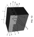
図1A~図1Qを参照すると、半導体ウェハ基板(基板とも称される)10のメモリセル領域2にメモリセルの対を作製し、基板10の論理デバイス領域4に論理デバイスを作製する、プロセスにおける工程の斜視断面図が示されている。プロセスは、半導体基板10の上面11に二酸化ケイ素12(酸化物とも称される)の層を形成することによって始まり、半導体基板10は、P型単結晶シリコンで形成され得る。酸化物層12は、堆積によって、又は熱酸化によって形成することができる。次いで、フォトリソグラフィマスキングプロセスを使用して、酸化物層12をパターン化する(すなわち、層のいくつかの部分を選択的に除去するが、他の部分は除去しない)。フォトリソグラフィマスキングプロセスは、酸化物層12にフォトレジスト材料をコーティングすることを含み、その後、フォトレジストを露光及び現像して、フォトレジストを論理デバイス領域4に維持しながらメモリセル領域2からフォトレジスト材料を除去する。次いで、酸化物エッチングを使用して、メモリセル領域2から酸化物層12の露出部分を除去し、基板10を露出したままにする(フォトレジストは、論理デバイス領域4内のエッチングから酸化物層12を保護する)。シリコンエッチングを使用して、メモリセル領域2内の基板10の露出した上面を窪ませる。酸化物層12及びフォトレジストは、このシリコンエッチングから論理デバイス領域4を保護する。この結果得られた構造体を図1Aに示し(フォトレジスト除去後)、図では、メモリセル領域2内の基板10の上面は、窪み量Rだけ論理デバイス領域4内の基板10の上面より下方に窪んでいる。
Referring to FIGS. 1A to 1Q, in the process of fabricating a pair of memory cells in a
酸化物層14をその構造体に形成する。酸化物層14に窒化シリコン(「窒化物」)層16を形成する。次いで、窒化物層16に絶縁層18(例えば、アモルファスカーボン)を形成する。フォトレジストを形成し、メモリセル及び論理デバイス領域2/4内のフォトレジストのストリップを選択的に除去し、絶縁層18の下地露出部分を除去して、下地窒化物層16まで下に延在して露出する絶縁層18にトレンチ20を形成することによって、絶縁層18をパターン化する。フォトレジストを除去した後、次いで、酸化物スペーサ22をトレンチ20内に形成する。スペーサの形成は、当該技術分野において周知である。その形成においては、構造体の輪郭に材料を堆積した後、異方性エッチング処理が行われる。その結果、その材料は、構造体の水平面からは除去され、構造体(丸みを帯びた上表面を有することが多い)の垂直配向面においては大部分がそのまま残存する。この場合、図1Bに示すように、酸化物スペーサ22は、トレンチ20の側壁に沿って形成される。
An
トレンチ20内の酸化物スペーサ22の部分を、構造をフォトレジストで覆うことによって除去し、その後、酸化物スペーサ22の部分が露出されるように、フォトレジストの部分的な除去を行う(例えば、メモリセル領域2内の特定のスペーサ22が完全に露出される一方で、論理デバイス領域4内の各スペーサ22の部分のみが露出されたままになる)。次いで、スペーサ22の露出部分を酸化物エッチングによって除去し、スペーサ22のセグメントをトレンチ20に残す。フォトレジストの除去後、絶縁層18の残りの部分を、それぞれのエッチング、例えば、カーボンエッチングによって除去する。次いで、窒化物エッチングを使用して、窒化物層16の露出部分(すなわち、残りの酸化物スペーサ22の下の窒化物層16の部分を除くすべて)を除去し、その後、酸化物エッチングにより、酸化物層14及び残りの酸化物スペーサ22の露出部分を除去する)。次いで、図1Cに示すように、シリコンエッチングを使用して、基板10の露出表面部分を窪ませて、メモリセル領域2にシリコン基板のフィン10aを形成し、論理デバイス領域4にシリコン基板のフィン10bを形成する。フィン10a及び10bは、下のバルクケイ素に対しては同じ高さを有するが、フィン10bは、窪み量Rだけフィン10aより垂直により高く延在する。
Portions of
その構造体を、酸化物(すなわち、STI酸化物)の厚い層24で覆い、次いで、(例えば、化学機械研磨-CMPによって)平坦化して、論理デバイス領域4内の窒化物層16の頂面を露出させる。平坦化された酸化物層24の上方に、窒化物層26を形成する。フォトレジストを、窒化物層26の上方に形成し、メモリセル領域2から除去する。エッチングを使用して、露出した窒化物層26/16及び酸化物層14を除去し、酸化物層24を、メモリセル領域2内のシリコンフィン10aの頂部の下方へと窪ませる。フォトレジストの除去後に、構造体に酸化物層28を形成する。第1のポリシリコン堆積によって、酸化物層28に、ポリシリコン(「ポリ」)層30を形成する。化学機械研磨を使用して、酸化物層28を停止層として使用してポリ層30を平坦化し、論理デバイス領域4からポリ層30を除去する。ポリエッチングバックを使用して、メモリセル領域2内のポリ層30を窪ませる。次いで、ポリ層30を、図1Dに示されるように、ポリ層30のストリップが残り、ストリップのそれぞれがメモリセル領域2内のフィン10aのうちの1つの頂部及び側壁に沿って延在するように、パターン化(フォトレジスト形成、露光、及び部分的な除去、その後のポリエッチング)する。
The structure is covered with a
構造体の上方に酸化物層32を形成し、酸化物層32の上方に窒化物層34を形成する。フォトレジストを、構造体の上方に形成し、メモリセル領域2から部分的に除去して、メモリセル領域2内のフィン10aを横切って延在する窒化物層34のストリップ部分を露出したままにする。窒化物エッチングを使用して窒化物層34の露出部分を除去し、酸化物エッチングを使用して酸化物層32の露出部分を除去し、メモリセル領域2内のポリ層30の部分を露出させる。図1E(フォトレジストの除去後)に示されるように、ポリエッチングを使用して、ポリ層30の露出部分を除去し、メモリセル領域2内のポリ層30のブロック30aを残す。
An
次いで、酸化物スペーサ36を酸化物堆積及び異方性エッチングによって形成して、ポリブロック30aの側壁を覆う。フォトレジストを、構造体の上方に形成し、部分的に除去して、メモリセル領域2の部分(すなわち、同じフィン10a上の隣接するポリブロック30a間の領域)を露出させる。埋め込みプロセスを実行して、隣接するポリブロック30a間のフィン10a内にソース領域52を形成する。等方性酸化物エッチングを使用して、ポリブロック30aの露出した側壁(すなわち、同じフィン10a上の隣接するポリブロック30aの互いに面する側壁)上の酸化物スペーサ36を除去する。フォトレジストの除去後、酸化物の層(トンネル酸化物)38を、ポリブロック30aの露出した側壁に(例えば、高温酸化-HTOにより)形成する。この結果得られた構造体を図1F(図1K及び図2によりよく示されるソース領域52を除く)に示す。この段階では、同じフィン10aに隣接するポリブロック30aについて、向かい合う側壁は、トンネル酸化物層38によって覆われ、互いから離れた側を向く側壁は、酸化物スペーサ36によって覆われている。
フォトレジストを、構造体の上方に形成し、部分的に除去して、メモリセル領域2の部分(すなわち、同じフィン10a上の隣接するポリブロック30aについて、互いから離れた側を向く側壁の周りの領域を露出させ、酸化物スペーサ36を露出したままにする)を露出させる。埋め込みプロセスを実行して、ポリブロック30aの側壁上の隣接する酸化物スペーサ36のフィン10aの部分に材料を埋め込む。フィン10aのこれらの埋め込まれた領域は、最終的には、後ほど形成されるワード線ゲートの下に配設される。次いで、酸化物エッチングを使用して、酸化物を除去し、埋め込まれたばかりのフィン10aの頂面及び側面部分を露出したままにする。フォトレジストの除去後、図1Gに示されるように、フィン10aの露出した頂面及び側面に酸化物層40(ワード線酸化物)を形成する。
A photoresist is formed over the structure and partially removed to remove portions of the memory cell area 2 (i.e. around the sidewalls facing away from each other for
フォトレジストを、構造体の上方に形成し、論理デバイス領域4から除去する。図1H(フォトレジスト除去後)に示されるように、一連のエッチングを実行して、酸化物及び窒化物層をSTI酸化物層24まで下に除去し、酸化物層24を窪ませ、これにより、フィン10bが論理デバイス領域4内で突出して部分的に露出する。次いで、酸化物層(図示せず)を形成して、論理デバイス領域4内のフィン10bの露出した頂面及び側面を覆う。次いで、第2のポリ堆積によって、ポリ層44を、構造体の上方に形成する。ポリ層44を、CMP(窒化物層34又は窒化物層34上の酸化物を、メモリセル領域内のポリブロック30aの上方で、CMP停止層として使用して)によって平坦化する。フォトレジストを、構造体に形成し、メモリセル領域2から除去する。等方性ポリエッチングを使用して、メモリセル領域2内のポリ層44を窪ませる。この結果得られた構造体を、図1I(フォトレジストの除去後)に示す。
A photoresist is formed over the structure and removed from the
フォトレジストを、構造体の上方に形成し、選択的に除去して、メモリセルと論理デバイス領域2/4の両方においてフィン10a/10bを横切って延在するフォトレジストのストリップを残す。ポリエッチングを使用して、ポリ層44の露出部分(フォトレジストのストリップの下のそれらの部分を除く)を除去する。フォトレジストの除去後、堆積及び異方性エッチングによって、スペーサ46を、ポリ層44の側面に形成する。スペーサ46を、好ましくはSiONなどの低K材料で形成する。この結果得られた構造体を図1Jに示す。メモリセル領域2では、ポリ層44のストリップ44a/44bは、それぞれがフィン10aを横切って延在し、ポリブロック30aに横方向に隣接したままである(すなわち、ポリブロック30aは、ストリップ44aと44bとの間にある)。論理デバイス領域では、ポリ層44のストリップ44cは、それぞれがフィン10bを横切って延在したままである(単純化のために1つのセットのフィン10b及び1つのストリップ44cのみが示されている)。
Photoresist is formed over the structure and selectively removed to leave a strip of photoresist extending across the
等方性エッチングを使用して、論理デバイス領域4内のポリストリップ44cに隣接するフィン10bを露出させる。ハードマスク層48(例えば、SiCN)を、構造体の上方に形成する。フォトレジスト50を、構造体に形成し、メモリセル領域2内の隣接するポリストリップ44aと隣接するポリストリップ44bとの間のハードマスク層48の部分と、論理デバイス領域4内のポリストリップ44cに隣接するハードマスク層48の部分と、を選択的に露出させるように、パターン化する。エッチングを使用して、メモリセル領域2内のハードマスク層48及び酸化物層40の露出部分を除去し、ポリストリップ44aと隣接するポリストリップ44bとの間のフィン10aの部分を露出させる。これらのエッチングはまた、論理デバイス領域4内のポリストリップ44cの両側のフィン10b上のハードマスク層48及び酸化物(以前に示されていない)の露出部分を除去する。次いで、埋め込みをメモリセル領域2内のフィン10aの露出部分に実行して、その中にドレイン領域53を形成する(及びソース領域52を増強する)。この埋め込みはまた、論理領域4のポリストリップ44cの両側のフィン10bにソース領域52L及びドレイン領域53Lを形成する。この結果得られた構造体を図1Kに示す(ソース/ドレイン領域52L/53Lを除く。それらは、図4によりよく示されている)。
An isotropic etch is used to expose
フォトレジスト50を除去した後、エピタキシャル層54を、メモリセル領域2内のフィン10aの露出したソース領域及びドレイン領域52/53、ならびに、論理デバイス領域4内のフィン10bの露出したソース領域及びドレイン領域52L/53L上で成長させる。エピタキシャル層54を、(より容易な接触形成及び信頼性のために)ソース/ドレイン領域のサイズを拡張し、より良好な伝導のためにフィン10a/10b内のキャリア移動度を増加させる。次いで、エッチングによって、ハードマスク層48の残りの部分を除去する。次いで、構造体を、窒化物56の層で覆う。酸化物58の厚い層を、構造体の上方に形成し、CMPによって平坦化する。この結果得られた構造体を図1Lに示す。
After removing the
フォトレジストを、構造体の上方に形成し、論理デバイス領域4から選択的に除去する。酸化物エッチングを使用して、ポリストリップ44cを露出させる。次いで、ポリエッチングを使用して、論理デバイス領域4からポリストリップ44cを除去する。フォトレジストの除去後、酸化物エッチングを使用して、以前にポリストリップ44cの下にあるフィン10b上の酸化物を除去し、論理デバイス領域4内のフィン10bの部分を露出させたままにする。次いで、図1Mに示すように、論理デバイス領域4内の露出したフィン10bを覆う酸化物層60を形成する。高K材料62の層(すなわち、HfO2、ZrO2、TiO2、Ta2O5、又は他の適切な材料などの酸化物より大きい誘電率Kを有する)を、構造体上(すなわち、酸化物層60上)に形成する。次いで、1つ以上の金属層を構造体に形成する。例えば、TiN層64を、構造体に形成し、続いてタングステン66の厚い層を形成し、続いて停止層として論理デバイス領域4内の高K層62を使用してCMPを行う。この結果得られた構造体を図1Nに示しており、論理デバイス領域4内の金属64/66のストリップはフィン10bを横切って延在している(以前に除去されたダミーポリストリップ44cを有効に置き換える)。
A photoresist is formed over the structure and selectively removed from the
窒化物層68を構造体の上方に形成し、酸化物層70を窒化物層68に形成する。フォトレジストを、構造体の上方に形成し、メモリセル領域2内のポリストリップ44bの上方で酸化物層70の部分を露出させるように、パターン化する。エッチングを実行して、酸化物層70、窒化物層68、及び酸化物層50の部分を除去し、ポリストリップ44bの頂部を露出させる。フォトレジストの除去後、Ti/Pt堆積及びアニールによって、サリサイド72を、ポリストリップ44bの頂面に形成する。必要に応じて、Tiエッチングによって、過剰なTiを除去する。酸化物73を、サリサイド72の上方の領域に充填するように堆積する。この結果得られた構造体を図1Oに示す。
A
フォトレジスト74を、構造体の上方に形成し、フォトレジスト74の部分をメモリ領域2内のソース/ドレイン領域52/53の垂直上方を除去し、論理デバイス領域4内のソース/ドレイン領域52L/53Lの垂直上方を除去するように、パターン化する。次いで、コンタクトホールを形成し、そこでは、フォトレジスト74が、それぞれのソース領域又はドレイン領域の下方に延在して露出する一連のエッチングによって除去されている。具体的には、メモリセル領域2内のコンタクトホール76はそれぞれ、ドレイン領域53のうちの1つまで下に延在し、それを露出させている。メモリ領域2内のコンタクトホール78(単純化のために1つのみが示されている)は、ソース領域52まで下に延在し、それを露出させている。論理デバイス領域4内のコンタクトホール80は、ソース領域52Lまで下に延在し、それを露出させている。論理デバイス領域4内のコンタクトホール82は、ドレイン領域53Lまで下に延在し、それを露出させている。この結果得られた構造体を図1Pに示す。
A
フォトレジスト74を除去した後、TiN層84を構造体に堆積させ、タングステン86の層をTiN層84に堆積させる。CMPを使用して、コンタクトホール76/78/80/82内以外の層84/86を除去する。コンタクトホール76内の層84/86は、ドレイン領域53まで下に延在し、かつそれと電気的に接触する、ドレイン接点88を形成する。コンタクトホール78内の層84/86は、ソース領域52まで下に延在し、かつそれと電気的に接触する、ソース接点90を形成する。コンタクトホール80内の層84/86は、ソース領域52Lまで下に延在し、かつそれと電気的に接触する、ソース接点92を形成する。コンタクトホール82内の層84/86は、ドレイン領域53Lまで下に延在し、かつそれと電気的に接触する、ドレイン接点94を形成する。最終構造体を図1Qに示す。さらなる接点処理の埋め込みをして、接点88/90/92/94を更に延在させて引き回し得る。
After removing the
図2は、メモリセル領域2内のフィン10aのうちの1つに沿って形成された一対のメモリセル100を示しているが、メモリセルの複数の追加の対が各フィン10a上で端から端まで形成されることを理解されたい。各メモリデバイス100は、ソース領域52及びドレイン領域53を含み、これらは、それらの間の半導体基板のチャネル領域96を画定する。チャネル領域96は、ソース領域及びドレイン領域52/53の間のフィン10aの側面及び頂面10c及び10dに沿って延在する。ポリブロック30aは、図3に最もよく示されているように、チャネル領域96の第1の部分の導電率を制御するために、フィン10aの側面及び頂面10c及び10dを取り囲み、かつそれから絶縁されている、浮遊ゲートである。同様に、ポリブロック44bは、図4に最もよく示されているように、チャネル領域96の第2の部分の導電率を制御するために、フィン10aの側面及び頂面10c及び10dを取り囲み、かつそれから絶縁されている、ワード線ゲートである。最後に、ポリブロック44aは、図5に最もよく示されているように、フィン10aのソース領域52を取り囲み、それから絶縁されている、消去ゲートである。ドレイン接点88及びソース接点90は、図2に更に示されている。
Although FIG. 2 shows a pair of
図6は、論理デバイス領域4のフィン10bのうちの1つに沿って形成された論理デバイス102の一部分を示し、これは、ソース領域52L及びドレイン領域53Lを含み、これらは、それらの間の半導体基板のチャネル領域98を画定する。チャネル領域98は、ソース領域及びドレイン領域52L/53Lの間のフィン10bの側面及び頂面10e及び10fに沿って延在している。TiN層64及びタングステン層66の残りは、図7に最もよく示されているように、チャネル領域98の導電率を制御するために、フィン10bの側面及び頂面10e及び10fを取り囲む、論理ゲートである。図中の論理デバイス102について、TiN層64及びタングステン層66の残りの部分によって形成された論理ゲート、ソース接点92及びドレイン接点94は、全て8つのフィン10bを横切って延在しており、これにより、8つのフィン10b上の8つのチャネル領域98が単一の論理デバイス102として同時に動作して、単一のフィンのみに形成された論理デバイスによって供給される動作電流を8回提供する。しかしながら、各論理デバイス102に含まれるフィンの数は、論理デバイスから必要な動作電流に応じて、任意の数(1つ以上)とすることができる。更に、論理領域4に1つの論理デバイス102のみが示されているが、同じ又は変動する電流容量の複数の論理デバイス102を論理領域4内で同時に形成することができる。
FIG. 6 shows a portion of the
同じ基板10に論理デバイス及びメモリセルを形成するための上記技術は、多くの利点を有する。第一に、メモリセルの3つのゲート(ポリブロック30aから形成された浮遊ゲート、ポリブロック44aから形成された消去ゲート、ポリブロック44bから形成されたワード線ゲート)は、フィン10aの頂面及び側面を取り囲むことで、それに見合った横方向サイズが大きくなることなく、チャネル領域96の有効領域を増加させることによって性能が向上し、これにより、メモリセルをより小さな横方向サイズにスケーリングすることを可能にする。第二に、論理デバイス102のTiN層64及びタングステン層66の残りの部分によって形成された論理ゲートは、フィン10bの頂面及び側面を取り囲み、それに見合った横方向サイズが大きくなることなく、チャネル領域98の有効領域を増加させることによって性能が向上し、これにより、論理デバイスをより小さな横方向サイズにスケーリングすることが可能にする。第三に、メモリセルは、(論理デバイス領域4に対して)基板10の窪んだメモリセル領域2に形成され、論理デバイス領域4内のより短い論理デバイスの高さを超えることなく、メモリセルのためにより厚いポリ層44を可能にし、両方の領域2/4における共通の形成工程を簡素化する。第四に、メモリセルの3つ全てのゲートを形成するために、2つのポリシリコン堆積のみが必要である。第五に、処理を簡素化するために、メモリ領域2内の、ワード線ゲート、すなわちポリブロック44b、及び消去ゲート、すなわちポリブロック44aを形成するために使用される同じポリシリコン堆積物も使用して、論理デバイス領域4(後に、TiN層64及びタングステン層66の残りの部分によって形成された金属論理ゲートと置き換えられる)内に、ダミーポリシリコンストリップ44c(すなわち、ダミーゲート)を形成する。第六に、ワード線ゲート、すなわちポリブロック44bの頂部は、メモリセル100の一列に対してポリブロック44bによって形成されたワード線ゲートを形成するポリシリコンのストリップに沿った電気抵抗を、サリサイドによって低減することができる。第七に、TiN層64及びタングステン層66の残りの部分によって形成された論理ゲートのための金属は、より高い導電率及び性能を提供し、その一方で、それぞれのポリブロック30a/44aによって形成されたメモリセルの浮遊ゲート及び消去ゲートのためのポリシリコンは、介在するトンネル酸化物38を介したトンネリングのより良好な制御を提供し、したがって、消去効率のより良好な制御を提供する。第八に、メモリセルのためのプロセス製造(メモリセルの3つ全てのポリゲートの形成を含む)の過半は、金属論理ゲートの形成の前に実行され、これは、CMOSベースラインへの処理の影響を低減する。第九に、メモリセルの一行に対してポリブロック44bによって形成されたワード線ゲートは、連続的なポリシリコンのストリップとして連続的に一緒に形成され、メモリセルの一行に対してポリブロック44aによって形成された消去ゲートは、ポリシリコンの連続ストリップとして連続的に形成され、複数のフィン10bのためのTiN層64の残りの部分及びタングステン層66によって形成された論理ゲートは、製造及びゲート相互接続を容易にするために、金属のストリップとして連続的に形成されている。
The above techniques for forming logic devices and memory cells on the
本発明は、上述の、及び本明細書に例証の実施形態(複数可)に限定されないことが理解されるべきである。例えば、本明細書で本発明に言及することは、任意の特許請求項又は特許請求項の用語の範囲を限定することを意図しておらず、その代わり、単に、1つ以上の特許請求項によって網羅され得る1つ以上の特徴に言及するものである。上記で説明した材料、プロセス、及び数値の実施例は、単に例示的なものであり、特許請求の範囲を限定するものとみなされるべきではない。更に、特許請求の範囲及び明細書から明らかであるように、全ての方法工程が例証又は特許請求される正確な順序で行われる必要はないが、むしろ本発明のメモリセル及び論理デバイスの適切な形成を可能にする任意の順序で(任意の順序で明示的に列挙された制限がない限り)行われる。最後に、単一層の材料をそのような又は同様の材料の複数層として形成することができ、逆もまた同様である。 It should be understood that the invention is not limited to the embodiment(s) described above and illustrated herein. For example, references herein to the invention are not intended to limit the scope of any claim or claim term, but instead merely refer to one or more claims. refers to one or more features that may be covered by. The material, process, and numerical examples described above are merely illustrative and should not be considered as limiting the scope of the claims. Furthermore, as is apparent from the claims and specification, not all method steps need be performed in the exact order illustrated or claimed, but rather in the appropriate order of the memory cells and logic devices of the present invention. in any order that allows for formation (unless there is an explicitly listed restriction on any order). Finally, a single layer of material can be formed as multiple layers of such or similar materials, and vice versa.
本明細書で使用される、「の上方に(over)」及び「に(on)」という用語は共に、「上に直接」(中間材料、要素、又は間隙がそれらの間に配設されていない)及び「上に間接的に」(中間材料、要素、又は間隙がそれらの間に配設されている)を包括的に含むことに留意されるべきである。同様に、「隣接した」という用語は、「直接隣接した」(中間材料、要素、又は間隙がそれらの間に配設されていない)、及び「間接的に隣接した」(中間材料、要素、又は間隙がそれらの間に配設されている)を含み、「に取り付けられた」は、「に直接取り付けられた」(中間材料、要素、又は間隙がそれらの間に配設されていない)、及び「に間接的に取り付けられた」(中間材料、要素、又は間隙がそれらの間に配設されている)を含み、「電気的に結合された」は、「直接電気的に結合された」(中間材料又は要素がそれらの間で要素を電気的に連結していない)、及び「間接的に電気的に結合された」(中間材料又は要素がそれらの間で要素を電気的に連結している)を含む。例えば、「基板の上方に」要素を形成することは、中間材料/要素が介在せずに直接基板にその要素を形成することも、1つ以上の中間材料/要素が介在して間接的に基板にその要素を形成することも含み得る。 As used herein, the terms "over" and "on" both mean "directly on" (with an intermediate material, element, or gap disposed between them) It should be noted that the term "indirectly on" (with an intermediate material, element, or gap disposed therebetween) is inclusive. Similarly, the term "adjacent" includes "directly adjacent" (no intermediate materials, elements, or gaps are disposed between them) and "indirectly adjacent" (intermediate materials, elements, "attached to" includes "attached directly to" (with no intermediate material, element, or gap disposed between them); , and “indirectly attached to” (with an intermediate material, element, or gap disposed between them), and “electrically coupled” means “directly electrically coupled to” "indirectly electrically coupled" (intermediate materials or elements do not electrically connect the elements between them), and "indirectly electrically coupled" (intermediate materials or elements do not electrically connect the elements between them); (concatenated). For example, forming an element "above the substrate" can mean forming the element directly on the substrate, without any intervening intermediate materials/elements, or indirectly, with one or more intervening intermediate materials/elements. It may also include forming the element on a substrate.
Claims (8)
上面を有し、第1の領域及び第2の領域を有するシリコン基板を提供するステップと、
前記シリコン基板の部分を除去して、前記シリコン基板の前記第1の領域において、上方に延在し、かつ頂面で終端する、一対の側面を有する上向きに延在する第1のシリコンフィンを形成し、前記シリコン基板の前記第2の領域において、上方に延在し、かつ頂面で終端する、一対の側面を有する上向きに延在する第2のシリコンフィンと、上方に延在し、かつ頂面で終端する一対の側面を有する上向きに延在する第3のシリコンフィンを形成する、除去するステップと、
第1の埋め込みを実行して、前記第1のシリコンフィンに第1のソース領域を形成する、実行するステップと、
第2の埋め込みを実行して、前記第1のシリコンフィンに第1のドレイン領域を形成し、前記第2のシリコンフィンに第2のソース領域及び第2のドレイン領域を、前記第3のシリコンフィンに第3のソース領域及び第3のドレイン領域を形成する、実行するステップであって、前記第1のソース領域及び前記第1のドレイン領域は、それらの間に延在する前記第1のシリコンフィンの第1のチャネル領域を画定し、前記第2のソース領域及び前記第2のドレイン領域は、それらの間に延在する前記第2のシリコンフィンの第2のチャネル領域を画定し、前記第3のソース領域及び前記第3のドレイン領域は、それらの間に延在する前記第3のシリコンフィンの第3のチャネル領域を画定する、実行するステップと、
第1のポリシリコン堆積を使用して、前記第1のチャネル領域の第1の部分の上方に配設され、かつそれから絶縁されている、浮遊ゲートを形成するステップであって、前記浮遊ゲートは、前記第1のシリコンフィンの前記頂面及び前記側面を取り囲んでいる、形成するステップと、
第2のポリシリコン堆積を使用して、前記第1のソース領域の上方に配設され、かつそれから絶縁されている、消去ゲートと、前記第1のチャネル領域の第2の部分の上方に配設され、かつそれから絶縁されている、ワード線ゲートと、前記第2のチャネル領域及び前記第3のチャネル領域の上方に配設され、かつそれらから絶縁されている、ダミーゲートと、を形成するステップであって、
前記消去ゲートは、前記第1のシリコンフィンの前記頂面及び前記側面を取り囲んでおり、
前記ワード線ゲートは、前記第1のシリコンフィンの前記頂面及び前記側面を取り囲んでおり、
前記ダミーゲートは、前記第2のシリコンフィンの前記頂面及び前記側面を取り囲み、前記第3のシリコンフィンの前記頂面及び前記側面を取り囲んでいる、形成するステップと、
前記ダミーゲートを、前記第2のチャネル領域及び前記第3のチャネル領域の上方に配設され、かつそれらから絶縁されている、金属ゲートで置き換えるステップであって、前記消去ゲート及びポリシリコンの前記ワード線ゲートを維持しながら、前記金属ゲートは、前記第2のシリコンフィンの前記頂面及び前記側面を取り囲み、前記第3のシリコンフィンの前記頂面及び前記側面を取り囲んでいる、置き換えるステップと、を含む、方法。 A method of forming a device, the method comprising:
providing a silicon substrate having a top surface and having a first region and a second region;
removing a portion of the silicon substrate to form an upwardly extending first silicon fin in the first region of the silicon substrate having a pair of side surfaces extending upwardly and terminating in a top surface; an upwardly extending second silicon fin formed and having a pair of side surfaces extending upwardly and terminating in a top surface in the second region of the silicon substrate; forming and removing a third upwardly extending silicon fin having a pair of side surfaces terminating in a top surface ;
performing a first implant to form a first source region in the first silicon fin;
performing a second implant to form a first drain region in the first silicon fin, a second source region and a second drain region in the second silicon fin , and a second implant in the third silicon fin; forming a third source region and a third drain region in a fin , the first source region and the first drain region having a third region extending therebetween; defining a first channel region of a silicon fin, the second source region and the second drain region defining a second channel region of the second silicon fin extending therebetween; the third source region and the third drain region define a third channel region of the third silicon fin extending therebetween;
forming a floating gate disposed over and insulated from a first portion of the first channel region using a first polysilicon deposition, the floating gate comprising: , surrounding the top surface and the side surfaces of the first silicon fin;
an erase gate disposed over and insulated from the first source region using a second polysilicon deposition and an erase gate disposed over a second portion of the first channel region; a word line gate disposed above and insulated from the second channel region and the third channel region; and a dummy gate disposed above and insulated from the second channel region and the third channel region. The step is to
the erase gate surrounds the top surface and the side surfaces of the first silicon fin;
the word line gate surrounds the top surface and the side surface of the first silicon fin;
forming the dummy gate surrounding the top surface and the side surface of the second silicon fin and surrounding the top surface and the side surface of the third silicon fin;
replacing the dummy gate with a metal gate disposed over and insulated from the second channel region and the third channel region ; the metal gate surrounds the top surface and the side surfaces of the second silicon fin, and the metal gate surrounds the top surface and the side surfaces of the third silicon fin, while maintaining a word line gate ; A method, including the steps of replacing.
前記シリコン基板の前記第2の領域内の前記上面を窪ませることなく、前記シリコン基板の前記第1の領域内の前記上面を窪ませるステップを更に含む、請求項1に記載の方法。 The portions of the silicon substrate in the first region and the second region of the silicon substrate are removed to form the upwardly extending first silicon fin and the upwardly extending second silicon fin. Before the removing step of forming a fin and the upwardly extending third silicon fin , the method includes:
2. The method of claim 1, further comprising recessing the top surface in the first region of the silicon substrate without recessing the top surface in the second region of the silicon substrate.
前記第2のチャネル領域及び前記第3のチャネル領域の上方から前記ダミーゲートを除去するステップと、
少なくとも1つの金属堆積を使用して、前記第2のチャネル領域及び前記第3のチャネル領域の上方にあり、かつそれらから絶縁されている、前記金属ゲートを形成するステップと、を含む、請求項1に記載の方法。 the step of replacing the dummy gate with the metal gate;
removing the dummy gate from above the second channel region and the third channel region ;
forming the metal gate over and insulated from the second channel region and the third channel region using at least one metal deposition. The method described in 1.
前記シリコン基板に第1の絶縁層を形成するステップと、
前記第1の絶縁層に第2の絶縁層を形成するステップと、
前記第2の絶縁層に材料のストリップを形成するステップと、
前記第2の絶縁層に、かつ前記材料のストリップに沿って、スペーサを形成するステップと、
前記材料のストリップを除去するステップと、
前記スペーサ間の前記第1の絶縁層及び前記第2の絶縁層の部分を除去して、前記シリコン基板の部分を露出させる、除去するステップと、
前記シリコン基板の露出した前記部分のエッチングを実行するステップと、を含む、請求項1に記載の方法。 The portion of the silicon substrate is removed to form the upwardly extending first silicon fin , the upwardly extending second silicon fin , and the upwardly extending third silicon fin. The forming and removing steps include:
forming a first insulating layer on the silicon substrate;
forming a second insulating layer on the first insulating layer;
forming a strip of material in the second insulating layer;
forming spacers in the second insulating layer and along the strip of material;
removing the strip of material;
removing a portion of the first insulating layer and the second insulating layer between the spacers to expose a portion of the silicon substrate;
2. The method of claim 1, comprising: performing an etch of the exposed portion of the silicon substrate.
the floating gate is insulated from the first portion of the first channel region by a first oxide layer, and the word line gate is insulated from the first portion of the first channel region by a first oxide layer; the metal gate is insulated from the second portion of the first channel region by a layer of high-K material and a third oxide layer different from the second oxide layer; 2. The method of claim 1, wherein the third channel region is insulated from the third channel region .
Applications Claiming Priority (3)
| Application Number | Priority Date | Filing Date | Title |
|---|---|---|---|
| US16/803,876 US11114451B1 (en) | 2020-02-27 | 2020-02-27 | Method of forming a device with FinFET split gate non-volatile memory cells and FinFET logic devices |
| US16/803,876 | 2020-02-27 | ||
| PCT/US2020/048835 WO2021173186A1 (en) | 2020-02-27 | 2020-08-31 | Method of forming a device with finfet split gate non-volatile memory cells and finfet logic devices |
Publications (2)
| Publication Number | Publication Date |
|---|---|
| JP2023505612A JP2023505612A (en) | 2023-02-09 |
| JP7364801B2 true JP7364801B2 (en) | 2023-10-18 |
Family
ID=72521715
Family Applications (1)
| Application Number | Title | Priority Date | Filing Date |
|---|---|---|---|
| JP2022550939A Active JP7364801B2 (en) | 2020-02-27 | 2020-08-31 | Method of forming a device comprising a FinFET split gate non-volatile memory cell and a FinFET logic device |
Country Status (7)
| Country | Link |
|---|---|
| US (1) | US11114451B1 (en) |
| EP (1) | EP4111500A1 (en) |
| JP (1) | JP7364801B2 (en) |
| KR (1) | KR20220114108A (en) |
| CN (1) | CN115152020B (en) |
| TW (1) | TWI748847B (en) |
| WO (1) | WO2021173186A1 (en) |
Families Citing this family (1)
| Publication number | Priority date | Publication date | Assignee | Title |
|---|---|---|---|---|
| US11362100B2 (en) * | 2020-03-24 | 2022-06-14 | Silicon Storage Technology, Inc. | FinFET split gate non-volatile memory cells with enhanced floating gate to floating gate capacitive coupling |
Citations (7)
| Publication number | Priority date | Publication date | Assignee | Title |
|---|---|---|---|---|
| US20150035039A1 (en) | 2013-07-31 | 2015-02-05 | Qualcomm Incorporated | Logic finfet high-k/conductive gate embedded multiple time programmable flash memory |
| US20160064398A1 (en) | 2014-09-02 | 2016-03-03 | Globalfoundries Singapore Pte. Ltd. | Integrated circuits with finfet nonvolatile memory |
| JP2017123398A (en) | 2016-01-07 | 2017-07-13 | ルネサスエレクトロニクス株式会社 | Semiconductor device and manufacturing method of the same |
| JP2017152541A (en) | 2016-02-24 | 2017-08-31 | ルネサスエレクトロニクス株式会社 | Semiconductor device manufacturing method |
| US20180151578A1 (en) | 2015-06-26 | 2018-05-31 | Intel Corporation | Semi-volatile embedded memory with between-fin floating-gate device and method |
| JP2018533228A (en) | 2015-11-03 | 2018-11-08 | シリコン ストーリッジ テクノロージー インコーポレイテッドSilicon Storage Technology, Inc. | Split gate nonvolatile flash memory cell having metal gate and method of manufacturing the same |
| US20200013786A1 (en) | 2018-07-05 | 2020-01-09 | Silicon Storage Technology, Inc. | Split Gate Non-Volatile Memory Cells With Three-Dimensional FINFET Structure, And Method Of Making Same |
Family Cites Families (16)
| Publication number | Priority date | Publication date | Assignee | Title |
|---|---|---|---|---|
| US6747310B2 (en) | 2002-10-07 | 2004-06-08 | Actrans System Inc. | Flash memory cells with separated self-aligned select and erase gates, and process of fabrication |
| US7315056B2 (en) | 2004-06-07 | 2008-01-01 | Silicon Storage Technology, Inc. | Semiconductor memory array of floating gate memory cells with program/erase and select gates |
| US7423310B2 (en) | 2004-09-29 | 2008-09-09 | Infineon Technologies Ag | Charge-trapping memory cell and charge-trapping memory device |
| KR101100428B1 (en) | 2005-09-23 | 2011-12-30 | 삼성전자주식회사 | Manufacturing method of Silicon Rich Oxide and Semiconductor adopting the same |
| US20090039410A1 (en) | 2007-08-06 | 2009-02-12 | Xian Liu | Split Gate Non-Volatile Flash Memory Cell Having A Floating Gate, Control Gate, Select Gate And An Erase Gate With An Overhang Over The Floating Gate, Array And Method Of Manufacturing |
| US8461640B2 (en) | 2009-09-08 | 2013-06-11 | Silicon Storage Technology, Inc. | FIN-FET non-volatile memory cell, and an array and method of manufacturing |
| US9634018B2 (en) | 2015-03-17 | 2017-04-25 | Silicon Storage Technology, Inc. | Split gate non-volatile memory cell with 3D finFET structure, and method of making same |
| US9570454B2 (en) * | 2015-06-25 | 2017-02-14 | Taiwan Semiconductor Manufacturing Co., Ltd. | Structure with emedded EFS3 and FinFET device |
| JP6578172B2 (en) * | 2015-09-18 | 2019-09-18 | ルネサスエレクトロニクス株式会社 | Semiconductor device |
| CN107305892B (en) | 2016-04-20 | 2020-10-02 | 硅存储技术公司 | Method of forming tri-gate non-volatile flash memory cell pairs using two polysilicon deposition steps |
| US9985042B2 (en) | 2016-05-24 | 2018-05-29 | Silicon Storage Technology, Inc. | Method of integrating FinFET CMOS devices with embedded nonvolatile memory cells |
| US10211217B2 (en) * | 2017-06-20 | 2019-02-19 | Taiwan Semiconductor Manufacturing Co., Ltd. | Method of manufacturing a semiconductor device and a semiconductor device |
| US10312247B1 (en) | 2018-03-22 | 2019-06-04 | Silicon Storage Technology, Inc. | Two transistor FinFET-based split gate non-volatile floating gate flash memory and method of fabrication |
| US10468428B1 (en) | 2018-04-19 | 2019-11-05 | Silicon Storage Technology, Inc. | Split gate non-volatile memory cells and logic devices with FinFET structure, and method of making same |
| TWI694592B (en) * | 2018-11-09 | 2020-05-21 | 物聯記憶體科技股份有限公司 | Non-volatile memory and manufacturing method thereof |
| US10886287B2 (en) * | 2019-01-14 | 2021-01-05 | Globalfoundries Inc. | Multiple-time programmable (MTP) memory device with a wrap-around control gate |
-
2020
- 2020-02-27 US US16/803,876 patent/US11114451B1/en active Active
- 2020-08-31 KR KR1020227027142A patent/KR20220114108A/en not_active IP Right Cessation
- 2020-08-31 CN CN202080097412.5A patent/CN115152020B/en active Active
- 2020-08-31 WO PCT/US2020/048835 patent/WO2021173186A1/en unknown
- 2020-08-31 JP JP2022550939A patent/JP7364801B2/en active Active
- 2020-08-31 EP EP20772479.0A patent/EP4111500A1/en not_active Withdrawn
-
2021
- 2021-01-20 TW TW110102042A patent/TWI748847B/en active
Patent Citations (7)
| Publication number | Priority date | Publication date | Assignee | Title |
|---|---|---|---|---|
| US20150035039A1 (en) | 2013-07-31 | 2015-02-05 | Qualcomm Incorporated | Logic finfet high-k/conductive gate embedded multiple time programmable flash memory |
| US20160064398A1 (en) | 2014-09-02 | 2016-03-03 | Globalfoundries Singapore Pte. Ltd. | Integrated circuits with finfet nonvolatile memory |
| US20180151578A1 (en) | 2015-06-26 | 2018-05-31 | Intel Corporation | Semi-volatile embedded memory with between-fin floating-gate device and method |
| JP2018533228A (en) | 2015-11-03 | 2018-11-08 | シリコン ストーリッジ テクノロージー インコーポレイテッドSilicon Storage Technology, Inc. | Split gate nonvolatile flash memory cell having metal gate and method of manufacturing the same |
| JP2017123398A (en) | 2016-01-07 | 2017-07-13 | ルネサスエレクトロニクス株式会社 | Semiconductor device and manufacturing method of the same |
| JP2017152541A (en) | 2016-02-24 | 2017-08-31 | ルネサスエレクトロニクス株式会社 | Semiconductor device manufacturing method |
| US20200013786A1 (en) | 2018-07-05 | 2020-01-09 | Silicon Storage Technology, Inc. | Split Gate Non-Volatile Memory Cells With Three-Dimensional FINFET Structure, And Method Of Making Same |
Also Published As
| Publication number | Publication date |
|---|---|
| TWI748847B (en) | 2021-12-01 |
| WO2021173186A1 (en) | 2021-09-02 |
| US20210272973A1 (en) | 2021-09-02 |
| JP2023505612A (en) | 2023-02-09 |
| EP4111500A1 (en) | 2023-01-04 |
| CN115152020A (en) | 2022-10-04 |
| KR20220114108A (en) | 2022-08-17 |
| US11114451B1 (en) | 2021-09-07 |
| TW202147580A (en) | 2021-12-16 |
| CN115152020B (en) | 2023-05-05 |
Similar Documents
| Publication | Publication Date | Title |
|---|---|---|
| TWI714011B (en) | Split gate non-volatile memory cells and logic devices with finfet structure, and method of making same | |
| US11594453B2 (en) | Method of forming a device with split gate non-volatile memory cells, HV devices having planar channel regions and FINFET logic devices | |
| TWI709247B (en) | Split gate non-volatile memory cells with three-dimensional finfet structure, and method of making same | |
| TWI757123B (en) | Finfet split gate non-volatile memory cells with enhanced floating gate to floating gate capacitive coupling | |
| JP7364801B2 (en) | Method of forming a device comprising a FinFET split gate non-volatile memory cell and a FinFET logic device | |
| US11315940B2 (en) | Method of forming a device with planar split gate non-volatile memory cells, high voltage devices and FinFET logic devices | |
| KR102567123B1 (en) | Method of Forming Devices with Isolated Plane Gate Non-Volatile Memory Cells, High Voltage Devices and FinFET Logic Devices | |
| US20230290864A1 (en) | Method of forming a device with planar split gate non-volatile memory cells, planar hv devices, and finfet logic devices on a substrate | |
| US20230189520A1 (en) | Split gate non-volatile memory cells, hv and logic devices with finfet structures, and method of making same | |
| WO2023172279A1 (en) | Method of forming a device with planar split gate non-volatile memory cells, planar hv devices, and finfet logic devices on a substrate |
Legal Events
| Date | Code | Title | Description |
|---|---|---|---|
| A521 | Request for written amendment filed |
Free format text: JAPANESE INTERMEDIATE CODE: A523 Effective date: 20221020 |
|
| A621 | Written request for application examination |
Free format text: JAPANESE INTERMEDIATE CODE: A621 Effective date: 20221020 |
|
| A871 | Explanation of circumstances concerning accelerated examination |
Free format text: JAPANESE INTERMEDIATE CODE: A871 Effective date: 20221020 |
|
| A131 | Notification of reasons for refusal |
Free format text: JAPANESE INTERMEDIATE CODE: A131 Effective date: 20230322 |
|
| A521 | Request for written amendment filed |
Free format text: JAPANESE INTERMEDIATE CODE: A523 Effective date: 20230622 |
|
| TRDD | Decision of grant or rejection written | ||
| A01 | Written decision to grant a patent or to grant a registration (utility model) |
Free format text: JAPANESE INTERMEDIATE CODE: A01 Effective date: 20230926 |
|
| A61 | First payment of annual fees (during grant procedure) |
Free format text: JAPANESE INTERMEDIATE CODE: A61 Effective date: 20231005 |
|
| R150 | Certificate of patent or registration of utility model |
Ref document number: 7364801 Country of ref document: JP Free format text: JAPANESE INTERMEDIATE CODE: R150 |