JP7351441B2 - Coil parts and method for manufacturing coil parts - Google Patents
Coil parts and method for manufacturing coil parts Download PDFInfo
- Publication number
- JP7351441B2 JP7351441B2 JP2023540834A JP2023540834A JP7351441B2 JP 7351441 B2 JP7351441 B2 JP 7351441B2 JP 2023540834 A JP2023540834 A JP 2023540834A JP 2023540834 A JP2023540834 A JP 2023540834A JP 7351441 B2 JP7351441 B2 JP 7351441B2
- Authority
- JP
- Japan
- Prior art keywords
- coil
- coil conductor
- line width
- bottom portion
- width direction
- Prior art date
- Legal status (The legal status is an assumption and is not a legal conclusion. Google has not performed a legal analysis and makes no representation as to the accuracy of the status listed.)
- Active
Links
- 238000004519 manufacturing process Methods 0.000 title claims description 26
- 238000000034 method Methods 0.000 title claims description 18
- 239000004020 conductor Substances 0.000 claims description 423
- 229920005989 resin Polymers 0.000 claims description 127
- 239000011347 resin Substances 0.000 claims description 127
- 238000002788 crimping Methods 0.000 claims description 2
- 239000010410 layer Substances 0.000 description 125
- 239000002184 metal Substances 0.000 description 28
- 229910052751 metal Inorganic materials 0.000 description 28
- 239000011229 interlayer Substances 0.000 description 20
- 239000011888 foil Substances 0.000 description 15
- 230000002093 peripheral effect Effects 0.000 description 15
- 239000011241 protective layer Substances 0.000 description 15
- 238000007747 plating Methods 0.000 description 14
- 238000012986 modification Methods 0.000 description 13
- 230000004048 modification Effects 0.000 description 13
- 102100038804 FK506-binding protein-like Human genes 0.000 description 11
- 101001031402 Homo sapiens FK506-binding protein-like Proteins 0.000 description 11
- 239000000463 material Substances 0.000 description 9
- 238000005530 etching Methods 0.000 description 8
- 230000000694 effects Effects 0.000 description 7
- 230000003746 surface roughness Effects 0.000 description 6
- 101100443272 Arabidopsis thaliana DIR2 gene Proteins 0.000 description 5
- 229920005992 thermoplastic resin Polymers 0.000 description 5
- 238000000605 extraction Methods 0.000 description 3
- RYGMFSIKBFXOCR-UHFFFAOYSA-N Copper Chemical compound [Cu] RYGMFSIKBFXOCR-UHFFFAOYSA-N 0.000 description 2
- 238000013459 approach Methods 0.000 description 2
- 238000004891 communication Methods 0.000 description 2
- 238000013461 design Methods 0.000 description 2
- 239000000696 magnetic material Substances 0.000 description 2
- 229920001343 polytetrafluoroethylene Polymers 0.000 description 2
- 239000004810 polytetrafluoroethylene Substances 0.000 description 2
- 229920000106 Liquid crystal polymer Polymers 0.000 description 1
- 239000004977 Liquid-crystal polymers (LCPs) Substances 0.000 description 1
- 239000004642 Polyimide Substances 0.000 description 1
- 239000000654 additive Substances 0.000 description 1
- 230000000996 additive effect Effects 0.000 description 1
- 230000015572 biosynthetic process Effects 0.000 description 1
- 229910052802 copper Inorganic materials 0.000 description 1
- 239000010949 copper Substances 0.000 description 1
- 239000011889 copper foil Substances 0.000 description 1
- 238000010438 heat treatment Methods 0.000 description 1
- 230000001678 irradiating effect Effects 0.000 description 1
- 239000000203 mixture Substances 0.000 description 1
- 229920001721 polyimide Polymers 0.000 description 1
- -1 polytetrafluoroethylene Polymers 0.000 description 1
- 239000000843 powder Substances 0.000 description 1
- 229910000679 solder Inorganic materials 0.000 description 1
Images


Classifications
-
- H—ELECTRICITY
- H01—ELECTRIC ELEMENTS
- H01F—MAGNETS; INDUCTANCES; TRANSFORMERS; SELECTION OF MATERIALS FOR THEIR MAGNETIC PROPERTIES
- H01F17/00—Fixed inductances of the signal type
-
- H—ELECTRICITY
- H01—ELECTRIC ELEMENTS
- H01F—MAGNETS; INDUCTANCES; TRANSFORMERS; SELECTION OF MATERIALS FOR THEIR MAGNETIC PROPERTIES
- H01F17/00—Fixed inductances of the signal type
- H01F17/04—Fixed inductances of the signal type with magnetic core
-
- H—ELECTRICITY
- H01—ELECTRIC ELEMENTS
- H01F—MAGNETS; INDUCTANCES; TRANSFORMERS; SELECTION OF MATERIALS FOR THEIR MAGNETIC PROPERTIES
- H01F27/00—Details of transformers or inductances, in general
- H01F27/28—Coils; Windings; Conductive connections
-
- H—ELECTRICITY
- H01—ELECTRIC ELEMENTS
- H01F—MAGNETS; INDUCTANCES; TRANSFORMERS; SELECTION OF MATERIALS FOR THEIR MAGNETIC PROPERTIES
- H01F41/00—Apparatus or processes specially adapted for manufacturing or assembling magnets, inductances or transformers; Apparatus or processes specially adapted for manufacturing materials characterised by their magnetic properties
- H01F41/02—Apparatus or processes specially adapted for manufacturing or assembling magnets, inductances or transformers; Apparatus or processes specially adapted for manufacturing materials characterised by their magnetic properties for manufacturing cores, coils, or magnets
- H01F41/04—Apparatus or processes specially adapted for manufacturing or assembling magnets, inductances or transformers; Apparatus or processes specially adapted for manufacturing materials characterised by their magnetic properties for manufacturing cores, coils, or magnets for manufacturing coils
Landscapes
- Engineering & Computer Science (AREA)
- Power Engineering (AREA)
- Microelectronics & Electronic Packaging (AREA)
- Manufacturing & Machinery (AREA)
- Coils Or Transformers For Communication (AREA)
Description
本発明は、コイルを備えるコイル部品に関する。 The present invention relates to a coil component including a coil.
従来のコイル部品に関する発明としては、例えば、特許文献1に記載の多層基板が知られている。この多層基板は、積層体及びコイルを備えている。積層体は、複数の基材層が積層された構造を有している。複数の基材層の材料は熱可塑性樹脂である。コイルは、積層体内に設けられている。コイルは、複数の基材層と共に積層されている複数のコイル導体パターンが層間接続導体により接続された構造を有している。このような多層基板は、熱可塑性樹脂を材料とする複数の基材層が熱圧着によって一体化されることにより、作製される。 As an invention related to a conventional coil component, for example, a multilayer board described in
ところで、特許文献1に記載の多層基板において、複数のコイル導体パターンの位置が設計値からずれることを抑制すると共に、コイルの直流抵抗値を低減したいという要望がある。 By the way, in the multilayer board described in
そこで、本発明の目的は、複数のコイル導体の位置が設計値からずれることを抑制できると共に、コイルの直流抵抗値を低減できるコイル部品及びコイル部品の製造方法を提供することである。 SUMMARY OF THE INVENTION Therefore, an object of the present invention is to provide a coil component and a method for manufacturing a coil component that can suppress the position of a plurality of coil conductors from deviating from a designed value and can reduce the DC resistance value of the coil.
本発明の一形態に係るコイル部品は、
上下方向の一方の方向が第1方向であり、上下方向の他方の方向が第2方向であり、
複数の樹脂層が上下方向に積層された構造を有する積層体と、
上下方向に見て線形状を有する複数のコイル導体を含んでいるコイルであって、上下方向に延びる中心軸線の周囲を周回する螺旋形状を有しているコイルであって、前記複数のコイル導体は、前記第2方向にこの順に並ぶ第1コイル導体、第2コイル導体及び第3コイル導体を含んでいる、コイルと、
を備えており、
前記第1コイル導体は、前記複数のコイル導体の中で最も前記第1方向に位置しており、
上下方向に見て、前記第1コイル導体、前記第2コイル導体及び前記第3コイル導体のそれぞれが延びる方向に直交する方向は、線幅方向であり、
前記第1コイル導体の外縁は、前記第1コイル導体の外縁において最も前記第2方向に位置する平面である第1ボトム部、及び、前記第1コイル導体の外縁において最も前記第1方向に位置する平面である第1トップ部を有しており、
前記第1トップ部の前記線幅方向の幅は、前記第1ボトム部の前記線幅方向の幅より小さく、
前記第2コイル導体の外縁は、前記第2コイル導体の外縁において最も前記第2方向に位置する平面である第2ボトム部、及び、前記第2コイル導体の外縁において最も前記第1方向に位置する平面である第2トップ部を有しており、
前記第2トップ部の前記線幅方向の幅は、前記第2ボトム部の前記線幅方向の幅より小さく、
前記第1トップ部と前記第1ボトム部との最短距離は、前記第2トップ部と前記第2ボトム部との最短距離より長く、
前記第1トップ部の前記線幅方向の幅を前記第1ボトム部の前記線幅方向の幅で割って得られる第1割合は、前記第2トップ部の前記線幅方向の幅を前記第2ボトム部の前記線幅方向の幅で割って得られる第2割合より小さい。A coil component according to one embodiment of the present invention includes:
One direction in the vertical direction is a first direction, the other direction in the vertical direction is a second direction,
A laminate having a structure in which a plurality of resin layers are stacked in the vertical direction;
A coil including a plurality of coil conductors having a linear shape when viewed in the vertical direction, the coil having a spiral shape circulating around a central axis extending in the vertical direction, the plurality of coil conductors a coil including a first coil conductor, a second coil conductor, and a third coil conductor arranged in this order in the second direction;
It is equipped with
The first coil conductor is located furthest in the first direction among the plurality of coil conductors,
When viewed in the vertical direction, the direction perpendicular to the direction in which each of the first coil conductor, the second coil conductor, and the third coil conductor extends is a line width direction,
The outer edge of the first coil conductor includes a first bottom portion which is a plane located furthest in the second direction at the outer edge of the first coil conductor, and a first bottom portion which is a plane located furthest in the first direction at the outer edge of the first coil conductor. has a first top portion that is a flat surface,
The width of the first top portion in the line width direction is smaller than the width of the first bottom portion in the line width direction,
The outer edge of the second coil conductor includes a second bottom portion which is a plane located furthest in the second direction at the outer edge of the second coil conductor, and a second bottom portion which is a plane located furthest in the first direction at the outer edge of the second coil conductor. It has a second top part that is a flat surface,
The width of the second top portion in the line width direction is smaller than the width of the second bottom portion in the line width direction,
The shortest distance between the first top part and the first bottom part is longer than the shortest distance between the second top part and the second bottom part,
A first ratio obtained by dividing the width of the first top portion in the line width direction by the width of the first bottom portion in the line width direction is calculated by dividing the width of the second top portion in the line width direction by the width of the second top portion in the line width direction. 2 is smaller than the second ratio obtained by dividing by the width of the bottom portion in the line width direction.
本発明の一形態に係るコイル部品の製造方法は、
上下方向の一方の方向が第1方向であり、上下方向の他方の方向が第2方向であり、
複数の樹脂層が上下方向に積層された構造を有する積層体と、
上下方向に見て線形状を有する複数のコイル導体を含んでいるコイルであって、上下方向に延びる中心軸線の周囲を周回する螺旋形状を有しているコイルであって、前記複数のコイル導体は、前記第2方向にこの順に並ぶ第1コイル導体、第2コイル導体及び第3コイル導体を含んでいる、コイルと、
を備える、
コイル部品の製造方法であって、
前記樹脂層に前記第2コイル導体を形成する第2コイル導体形成工程と、
前記第2コイル導体形成工程の後に、前記複数の樹脂層を熱圧着する熱圧着工程と、
前記熱圧着工程の後に、前記熱圧着工程において熱圧着した前記複数の樹脂層の中で最も前記第1方向に位置する前記樹脂層に位置する前記第1コイル導体の上下方向の厚みを大きくする第1コイル導体形成工程と、
前記熱圧着工程の後に、前記熱圧着工程において熱圧着した前記複数の樹脂層の中で最も前記第2方向に位置する前記樹脂層に位置する前記第3コイル導体の上下方向の厚みを大きくする第3コイル導体形成工程と、
を備えており、
上下方向に見て、前記第1コイル導体、前記第2コイル導体及び前記第3コイル導体のそれぞれが延びる方向に直交する方向は、線幅方向であり、
前記第1コイル導体の外縁は、前記第1コイル導体の外縁において最も前記第2方向に位置する平面である第1ボトム部、及び、前記第1コイル導体の外縁において最も前記第1方向に位置する平面である第1トップ部を有しており、
前記第1トップ部の前記線幅方向の幅は、前記第1ボトム部の前記線幅方向の幅より小さく、
前記第2コイル導体の外縁は、前記第2コイル導体の外縁において最も前記第2方向に位置する平面である第2ボトム部、及び、前記第2コイル導体の外縁において最も前記第1方向に位置する平面である第2トップ部を有しており、
前記第2トップ部の前記線幅方向の幅は、前記第2ボトム部の前記線幅方向の幅より小さく、
前記第1トップ部と前記第1ボトム部との最短距離は、前記第2トップ部と前記第2ボトム部との最短距離より長く、
前記第1トップ部の前記線幅方向の幅を前記第1ボトム部の前記線幅方向の幅で割って得られる第1割合は、前記第2トップ部の前記線幅方向の幅を前記第2ボトム部の前記線幅方向の幅で割って得られる第2割合より小さい。A method for manufacturing a coil component according to one embodiment of the present invention includes:
One direction in the vertical direction is a first direction, the other direction in the vertical direction is a second direction,
A laminate having a structure in which a plurality of resin layers are stacked in the vertical direction;
A coil including a plurality of coil conductors having a linear shape when viewed in the vertical direction, the coil having a spiral shape circulating around a central axis extending in the vertical direction, the plurality of coil conductors a coil including a first coil conductor, a second coil conductor, and a third coil conductor arranged in this order in the second direction;
Equipped with
A method for manufacturing a coil component,
a second coil conductor forming step of forming the second coil conductor on the resin layer;
a thermocompression bonding step of thermocompression bonding the plurality of resin layers after the second coil conductor forming step;
After the thermocompression bonding step, the vertical thickness of the first coil conductor located in the resin layer located in the first direction among the plurality of resin layers thermocompression bonded in the thermocompression bonding step is increased. A first coil conductor forming step;
After the thermocompression bonding step, the thickness in the vertical direction of the third coil conductor located in the resin layer located in the second direction most among the plurality of resin layers thermocompression bonded in the thermocompression bonding step is increased. A third coil conductor forming step,
It is equipped with
When viewed in the vertical direction, the direction perpendicular to the direction in which each of the first coil conductor, the second coil conductor, and the third coil conductor extends is a line width direction,
The outer edge of the first coil conductor includes a first bottom portion which is a plane located furthest in the second direction at the outer edge of the first coil conductor, and a first bottom portion which is a plane located furthest in the first direction at the outer edge of the first coil conductor. has a first top portion that is a flat surface,
The width of the first top portion in the line width direction is smaller than the width of the first bottom portion in the line width direction,
The outer edge of the second coil conductor includes a second bottom portion which is a plane located furthest in the second direction at the outer edge of the second coil conductor, and a second bottom portion which is a plane located furthest in the first direction at the outer edge of the second coil conductor. It has a second top part that is a flat surface,
The width of the second top portion in the line width direction is smaller than the width of the second bottom portion in the line width direction,
The shortest distance between the first top part and the first bottom part is longer than the shortest distance between the second top part and the second bottom part,
A first ratio obtained by dividing the width of the first top portion in the line width direction by the width of the first bottom portion in the line width direction is calculated by dividing the width of the second top portion in the line width direction by the width of the first bottom portion in the line width direction. 2 is smaller than the second ratio obtained by dividing by the width of the bottom portion in the line width direction.
本発明の一形態に係るコイル部品の製造方法は、
上下方向の一方の方向が第1方向であり、上下方向の他方の方向が第2方向であり、
複数の樹脂層が上下方向に積層された構造を有する積層体と、
上下方向に見て線形状を有する複数のコイル導体を含んでいるコイルであって、上下方向に延びる中心軸線の周囲を周回する螺旋形状を有しているコイルであって、前記複数のコイル導体は、前記第2方向にこの順に並ぶ第1コイル導体、第2コイル導体及び第3コイル導体を含んでいる、コイルと、
を備える、
コイル部品の製造方法であって、
前記樹脂層に前記第2コイル導体を形成する第2コイル導体形成工程と、
前記樹脂層に前記第3コイル導体を形成する第3コイル導体形成工程と、
前記第2コイル導体形成工程及び前記第3コイル導体形成工程の後に、前記第2コイル導体及び前記第3コイル導体が前記第2方向にこの順に並ぶように前記複数の樹脂層を熱圧着する熱圧着工程と、
前記熱圧着工程の後に、前記熱圧着工程において熱圧着した前記複数の樹脂層の中で最も前記第1方向に位置する前記樹脂層に位置する前記第1コイル導体の上下方向の厚みを大きくする第1コイル導体形成工程と、
を備えており、
上下方向に見て、前記第1コイル導体、前記第2コイル導体及び前記第3コイル導体のそれぞれが延びる方向に直交する方向は、線幅方向であり、
前記第1コイル導体の外縁は、前記第1コイル導体の外縁において最も前記第2方向に位置する平面である第1ボトム部、及び、前記第1コイル導体の外縁において最も前記第1方向に位置する平面である第1トップ部を有しており、
前記第1トップ部の前記線幅方向の幅は、前記第1ボトム部の前記線幅方向の幅より小さく、
前記第2コイル導体の外縁は、前記第2コイル導体の外縁において最も前記第2方向に位置する平面である第2ボトム部、及び、前記第2コイル導体の外縁において最も前記第1方向に位置する平面である第2トップ部を有しており、
前記第2トップ部の前記線幅方向の幅は、前記第2ボトム部の前記線幅方向の幅より小さく、
前記第1トップ部と前記第1ボトム部との最短距離は、前記第2トップ部と前記第2ボトム部との最短距離より長く、
前記第1トップ部の前記線幅方向の幅を前記第1ボトム部の前記線幅方向の幅で割って得られる第1割合は、前記第2トップ部の前記線幅方向の幅を前記第2ボトム部の前記線幅方向の幅で割って得られる第2割合より小さい。A method for manufacturing a coil component according to one embodiment of the present invention includes:
One direction in the vertical direction is a first direction, the other direction in the vertical direction is a second direction,
A laminate having a structure in which a plurality of resin layers are stacked in the vertical direction;
A coil including a plurality of coil conductors having a linear shape when viewed in the vertical direction, the coil having a spiral shape circulating around a central axis extending in the vertical direction, the plurality of coil conductors a coil including a first coil conductor, a second coil conductor, and a third coil conductor arranged in this order in the second direction;
Equipped with
A method for manufacturing a coil component,
a second coil conductor forming step of forming the second coil conductor on the resin layer;
a third coil conductor forming step of forming the third coil conductor on the resin layer;
After the second coil conductor forming step and the third coil conductor forming step, heat-bonding the plurality of resin layers by thermocompression so that the second coil conductor and the third coil conductor are lined up in this order in the second direction. crimping process,
After the thermocompression bonding step, the vertical thickness of the first coil conductor located in the resin layer located in the first direction among the plurality of resin layers thermocompression bonded in the thermocompression bonding step is increased. A first coil conductor forming step;
It is equipped with
When viewed in the vertical direction, the direction perpendicular to the direction in which each of the first coil conductor, the second coil conductor, and the third coil conductor extends is a line width direction,
The outer edge of the first coil conductor includes a first bottom portion which is a plane located furthest in the second direction at the outer edge of the first coil conductor, and a first bottom portion which is a plane located furthest in the first direction at the outer edge of the first coil conductor. has a first top portion that is a flat surface,
The width of the first top portion in the line width direction is smaller than the width of the first bottom portion in the line width direction,
The outer edge of the second coil conductor includes a second bottom portion which is a plane located furthest in the second direction at the outer edge of the second coil conductor, and a second bottom portion which is a plane located furthest in the first direction at the outer edge of the second coil conductor. It has a second top part that is a flat surface,
The width of the second top portion in the line width direction is smaller than the width of the second bottom portion in the line width direction,
The shortest distance between the first top part and the first bottom part is longer than the shortest distance between the second top part and the second bottom part,
A first ratio obtained by dividing the width of the first top portion in the line width direction by the width of the first bottom portion in the line width direction is calculated by dividing the width of the second top portion in the line width direction by the width of the second top portion in the line width direction. 2 is smaller than the second ratio obtained by dividing by the width of the bottom portion in the line width direction.
本発明に係るコイル部品によれば、複数のコイル導体が設計値からずれることを抑制できると共に、コイルの直流抵抗値を低減できる。 According to the coil component according to the present invention, it is possible to prevent the plurality of coil conductors from deviating from the designed value, and it is also possible to reduce the DC resistance value of the coil.
(実施形態)
[駆動モジュールの構造]
以下に、本発明の実施形態に係る駆動モジュール10の構造について図面を参照しながら説明する。図1は、コイル部品11を備える駆動モジュール10の断面図である。図2は、コイル部品11の分解斜視図である。(Embodiment)
[Structure of drive module]
Below, the structure of the
本明細書において、方向を以下のように定義する。コイル部品11の積層体12の積層方向を上下方向と定義する。上下方向の一方である上方向が第1方向DIR1である。上下方向の他方である下方向が第2方向DIR2である。また、左右方向及び前後方向は、上下方向に直交している。左右方向は、前後方向に直交している。なお、本実施形態における上下方向、前後方向及び左右方向は、駆動モジュール10の使用時における上下方向、前後方向及び左右方向と一致していなくてもよい。 In this specification, direction is defined as follows. The stacking direction of the stacked
以下では、Xは、駆動モジュール10の部品又は部材である。本明細書において、特に断りのない場合には、Xの各部について以下のように定義する。Xの前部とは、Xの前半分を意味する。Xの後部とは、Xの後半分を意味する。Xの左部とは、Xの左半分を意味する。Xの右部とは、Xの右半分を意味する。Xの上部とは、Xの上半分を意味する。Xの下部とは、Xの下半分を意味する。Xの前端とは、Xの前方向の端を意味する。Xの後端とは、Xの後方向の端を意味する。Xの左端とは、Xの左方向の端を意味する。Xの右端とは、Xの右方向の端を意味する。Xの上端とは、Xの上方向の端を意味する。Xの下端とは、Xの下方向の端を意味する。Xの前端部とは、Xの前端及びその近傍を意味する。Xの後端部とは、Xの後端及びその近傍を意味する。Xの左端部とは、Xの左端及びその近傍を意味する。Xの右端部とは、Xの右端及びその近傍を意味する。Xの上端部とは、Xの上端及びその近傍を意味する。Xの下端部とは、Xの下端及びその近傍を意味する。 In the following, X is a part or member of the
まず、図1を参照しながら、駆動モジュール10及びコイル部品11の構造について説明する。駆動モジュール10は、例えば、スマートフォン等の無線通信端末に用いられる。 First, the structures of the
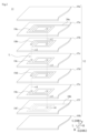
駆動モジュール10は、図1及び図2に示すように、コイル部品11及び磁石50を備えている。コイル部品11は、積層体12、コイルL及び引き出し導体20a,20bを備えている。積層体12は、樹脂層15a~15fが上下方向に積層された構造を有している。本実施形態では、積層体12は、樹脂層15a~15f及び保護層16a,16bを含んでいる。保護層16a、樹脂層15a~15f及び保護層16bは、上から下へとこの順に並んでいる。 The
樹脂層15a~15fのそれぞれは、図2に示すように、上下方向に並ぶ上主面及び下主面を有している。樹脂層15a~15fの材料は、熱可塑性樹脂である。熱可塑性樹脂は、例えば、液晶ポリマー、PTFE(ポリテトラフロオロエチレン)等の熱可塑性樹脂である。樹脂層15a~15fの材料は、ポリイミドであってもよい。従って、積層体12の材料は、非磁性材料である。 As shown in FIG. 2, each of the resin layers 15a to 15f has an upper main surface and a lower main surface that are arranged in the vertical direction. The material of the resin layers 15a to 15f is thermoplastic resin. The thermoplastic resin is, for example, a liquid crystal polymer, PTFE (polytetrafluoroethylene), or the like. The material of the resin layers 15a to 15f may be polyimide. Therefore, the material of the laminate 12 is a non-magnetic material.
保護層16a,16bは、レジスト層である。保護層16aは、樹脂層15aの上主面に位置している。保護層16aは、樹脂層15aの上主面に位置するコイル導体18aを保護している。保護層16bは、樹脂層15fの下主面に位置している。保護層16bは、樹脂層15fの下主面に位置するコイル導体18fを保護している。保護層16a,16bのそれぞれは、絶縁性のシートが樹脂層15aの上主面及び樹脂層15fの下主面に貼り付けられることにより形成されてもよいし、絶縁性の樹脂ペーストが樹脂層15aの上主面及び樹脂層15bの下主面に印刷されることにより形成されてもよい。 The
コイルLは、積層体12に設けられている。コイルLは、図1及び図2に示すように、
上下方向に延びる中心軸線Ax1の周囲を周回する螺旋形状を有している。本実施形態では、コイルLは、時計回りに周回しながら上方向に進行する螺旋形状を有している。コイルLは、上下方向に見て線形状を有する複数のコイル導体を含んでいる。複数のコイル導体は、下方向(第2方向DIR2)にこの順に並ぶコイル導体18a(第1コイル導体)、コイル導体18b~18e(第2コイル導体)及びコイル導体18f(第3コイル導体)を含んでいる。本実施形態では、コイルLは、図2に示すように、コイル導体18a~18f及び層間接続導体v1~v6を含んでいる。The coil L is provided in the
It has a spiral shape that revolves around a central axis Ax1 extending in the vertical direction. In this embodiment, the coil L has a spiral shape that moves upward while rotating clockwise. The coil L includes a plurality of coil conductors having a linear shape when viewed in the vertical direction. The plurality of coil conductors include a
コイル導体18a~18fは、樹脂層15a~15fと共に上下方向に積層されている。より詳細には、コイル導体18a~18eのそれぞれは、樹脂層15a~15eの上主面に位置している。コイル導体18fは、樹脂層15fの下主面に位置している。これにより、コイル導体18a~18fは、上から下へとこの順に並んでいる。また、コイル導体18a(第1コイル導体)は、コイル導体18a~18fの中で最も上(第1方向DIR1)に位置している。コイル導体18f(第3コイル導体)は、コイル導体18a~18fの中で最も下(第2方向DIR2)に位置している。 The
コイル導体18a~18f(第1コイル導体、第2コイル導体及び第3コイル導体)のそれぞれは、上下方向に見て、中心軸線Ax1を中心に1周以上にわたって周回する渦巻形状を有している。本実施形態では、コイル導体18a,18c,18eは、下方向に見て、反時計回りに周回しながら中心に近づく渦巻形状を有している。コイル導体18b,18d,18fは、下方向に見て、時計回りに周回しながら中心に近づく渦巻形状を有している。以下では、コイル導体18a~18fの外周側の端部を外周端部と呼ぶ。コイル導体18a~18fの内周側の端部を内周端部と呼ぶ。 Each of the
層間接続導体v1~v6のそれぞれは、樹脂層15a~15fを上下方向に貫通している。層間接続導体v1は、コイル導体18aの内周端部とコイル導体18bの内周端部とを電気的に接続している。層間接続導体v2は、コイル導体18bの外周端部とコイル導体18cの外周端部とを電気的に接続している。層間接続導体v3は、コイル導体18cの内周端部とコイル導体18dの内周端部とを電気的に接続している。層間接続導体v4は、コイル導体18dの外周端部とコイル導体18eの外周端部とを電気的に接続している。層間接続導体v5と層間接続導体v6は、直列に接続されている。層間接続導体v5,v6は、コイル導体18eの内周端部とコイル導体18fの内周端部とを電気的に接続している。 Each of the interlayer connection conductors v1 to v6 vertically penetrates the resin layers 15a to 15f. The interlayer connection conductor v1 electrically connects the inner peripheral end of the
引き出し導体20aは、樹脂層15aの上主面に位置している。引き出し導体20aは、コイル導体18aの外周端部に接続されている。また、引き出し導体20aは、コイル導体18aの外周端部から右方向に延びている。これにより、引き出し導体20aは、コイル導体18a~18fの周回軌道から離脱することにより、コイルLから離れている。 The
引き出し導体20bは、樹脂層15fの下主面に位置している。引き出し導体20bは、コイル導体18fの外周端部に接続されている。また、引き出し導体20bは、コイル導体18fの外周端部から右方向に延びている。これにより、引き出し導体20bは、コイル導体18a~18fの周回軌道から離脱することにより、コイルLから離れている。 The
以上のようなコイル導体18b~18eのそれぞれは、樹脂層15b~15eの上主面に貼り付けられた金属箔にエッチングが施されることにより形成された導体層である。金属箔は、例えば、銅箔である。コイル導体18a,18fのそれぞれは、樹脂層15aの上主面及び樹脂層15bの下主面にメッキが施されることにより形成された導体層である。メッキは、例えば、銅メッキである。また、層間接続導体v1~v6は、樹脂層15a~15eに形成した貫通孔に導電性ペーストを充填し、加熱により導電性ペーストを固化させることにより形成される。導電性ペーストは、例えば、金属粉末と樹脂との混合物である。なお、層間接続導体v1~v6は、樹脂層15a~15eに形成した貫通孔の内周面にメッキを施すことにより形成されてもよい。 Each of the
ここで、図1に示すように、コイル導体18a(第1コイル導体)の上下方向の厚みT1は、コイル導体18b~18e(第2コイル導体)の上下方向の厚みT2より大きい(長い)(関係1)。厚みT1は、後述する第1トップ部S2と第1ボトム部S1との最短距離である。厚みT2は、後述する第2トップ部S4と第2ボトム部S3との最短距離である。また、コイル導体18f(第3コイル導体)の上下方向の厚みT3は、コイル導体18b~18e(第2コイル導体)の上下方向の厚みT2より大きい(長い)(関係2)。厚みT3は、後述する第3トップ部S6と第3ボトム部S5との最短距離である。コイル導体18b~18e(第2コイル導体)は、コイル導体18a~18fの内の最も上に位置するコイル導体18a及び最も下に位置するコイル導体18fを除いたコイル導体を指している。 Here, as shown in FIG. 1, the vertical thickness T1 of the
また、上記関係1及び関係2は、上下方向に平行なコイル部品11の複数の断面の内の全ての断面において成立していてもよいし、上下方向に平行なコイル部品11の複数の断面の内の少なくとも1つの断面において成立していてもよい。また、コイル導体18aの上下方向の厚みT1は、コイル導体18aの上下方向の厚みT1の平均値である。なお、厚みT2,T3の定義も、厚みT1の定義と同様である。 Moreover, the
ところで、上下方向に見て、コイル導体18a~18f(第1コイル導体、第2コイル導体及び第3コイル導体)のそれぞれが延びる方向に直交する方向は、線幅方向である。コイル導体18a(第1コイル導体)の外縁は、コイル導体18a(第1コイル導体)の外縁において最も下(第2方向)に位置する平面である第1ボトム部S1、及び、コイル導体18a(第1コイル導体)の外縁において最も上(第1方向)に位置する平面である第1トップ部S2を有している。第1トップ部S2は、第1ボトム部S1より上(第1方向DIR1)に位置し、第1ボトム部S1と平行な法線を有している。本実施形態では、第1トップ部S2は、平面である。第1ボトム部S1は、樹脂層15aの上主面に固定されている。また、第1ボトム部S1の表面粗さは、第1トップ部S2の表面粗さよりも大きい。そして、第1トップ部S2の線幅方向の幅W2は、第1ボトム部S1の線幅方向の幅W1より小さい。 By the way, when viewed in the vertical direction, the direction perpendicular to the direction in which each of the
コイル導体18b~18e(第2コイル導体)の外縁のそれぞれは、コイル導体18b~18e(第2コイル導体)の外縁において最も下(第2方向)に位置する平面である第2ボトム部S3、及び、コイル導体18b~18e(第2コイル導体)の外縁において最も上(第1方向)に位置する平面である第2トップ部S4を有している。第2トップ部S4は、第2ボトム部S3より上(第1方向DIR1)に位置し、第2ボトム部S3と平行な法線を有している。コイル導体18b~18eの第2ボトム部S3のそれぞれは、樹脂層15b~15eの上主面に固定されている。また、第2ボトム部S3の表面粗さは、第2トップ部S4の表面粗さよりも大きい。そして、第2トップ部S4の線幅方向の幅W4は、第2ボトム部S3の線幅方向の幅W3より小さい。また、本実施形態では、第2ボトム部S3の線幅方向の幅W3は、第1ボトム部S1の線幅方向の幅W1と等しい。第2トップ部S4の線幅方向の幅W4は、第1トップ部S2の線幅方向の幅W2より大きい。従って、第1トップ部S2の線幅方向の幅W2を第1ボトム部S1の線幅方向の幅W1で割って得られる第1割合P1は、第2トップ部S4の線幅方向の幅W4を第2ボトム部S3の線幅方向の幅W3で割って得られる第2割合P2より小さい(関係3)。 Each of the outer edges of the
コイル導体18f(第3コイル導体)の外縁は、コイル導体18f(第3コイル導体)の外縁において最も下(第2方向)に位置する平面である第3ボトム部S5、及び、コイル導体18f(第3コイル導体)の外縁において最も上(第1方向)に位置する平面である第3トップ部S6を有している。第3トップ部S6は、第3ボトム部S5より上(第1方向DIR1)に位置し、第3ボトム部S5と平行な法線を有している。第3ボトム部S5は、樹脂層15fの下主面に固定されている。また、第3ボトム部S5の表面粗さは、第3トップ部S6の表面粗さよりも大きい。そして、第3トップ部S6の線幅方向の幅W6は、第3ボトム部S5の線幅方向の幅W5より小さい。また、本実施形態では、第2ボトム部S3の線幅方向の幅W3は、第3ボトム部S5の線幅方向の幅W5と等しい。第2トップ部S4の線幅方向の幅W4は、第3トップ部S6の線幅方向の幅W6より大きい。従って、第3トップ部S6の線幅方向の幅W6を第3ボトム部S5の線幅方向の幅W5で割って得られる第3割合P3は、第2割合P2より小さい(関係4)。 The outer edge of the
なお、上記関係3及び関係4は、上下方向に平行なコイル部品11の複数の断面の内の全ての断面において成立していてもよいし、上下方向に平行なコイル部品11の複数の断面の内の少なくとも1つの断面において成立していてもよい。また、第1ボトム部S1の線幅方向の幅W1は、コイル導体18aの線幅方向の幅W1の平均値であってもよい。幅W2~W6の定義も、幅W1の定義と同じである。 Incidentally, the
磁石50は、図1に示すように、コイルLより上(第1方向DIR1)に位置している。磁石50は、上下方向に見て、コイルLと重なっている。以上のような磁石50は、左右方向に延びている。磁石50の左部は、N極である。磁石50の右部は、S極である。 As shown in FIG. 1, the
また、駆動モジュール10は、図示しない磁気センサを更に備えている。磁気センサは、磁石50の磁力を検知する。磁気センサは、例えば、積層体12に実装されている。 Further, the
以上のような駆動モジュール10は、図示しない制御回路を備えている。磁気センサ及びコイルLは、制御回路に電気的に接続されている。磁気センサは、磁気センサにより検知された磁力の大きさに応じた出力信号を生成する。制御回路は、磁気センサが生成した出力信号に基づいて、コイルLに流す電流の大きさを制御する。例えば、下方向に見て、コイルLに時計回り方向の電流が流れると、コイルLの左部に位置する導体には前方向に電流が流れ、コイルLの右部に位置する導体には後方向に電流が流れる。磁石50では、N極から磁力線が出ると共に、S極へと磁力線が入る。従って、コイルLの左部に位置する導体に前方向に電流が流れると、コイルLの左部に位置する導体は、左方向にローレンツ力を受ける。コイルLの右部に位置する導体に後方向に電流が流れると、コイルLの右部に位置する導体は、左方向にローレンツ力を受ける。すなわち、コイルLは、磁石50から左方向に力を受ける。換言すれば、磁石50は、コイルLから右方向に力を受ける。その結果、磁石50は、コイルLに対して右方向に変位する。ただし、コイルLが、磁石50に対して左方向に変位してもよい。 The
一方、下方向に見て、コイルLに反時計回り方向の電流が流れると、コイルLの左部に位置する導体には後方向に電流が流れ、コイルLの右部に位置する導体には前方向に電流が流れる。コイルLの左部に位置する導体に後方向に電流が流れると、コイルLの左部に位置する導体は、右方向にローレンツ力を受ける。コイルLの右部に位置する導体に前方向に電流が流れると、コイルLの右部に位置する導体は、右方向にローレンツ力を受ける。すなわち、コイルLは、磁石50から右方向に力を受ける。換言すれば、磁石50は、コイルLから左方向に力を受ける。その結果、磁石50は、コイルLに対して左方向に変位する。以上のように、コイルLが発生する磁力により、磁石50のコイルLに対する位置が変化する。ただし、コイルLが、磁石50に対して右方向に変位してもよい。 On the other hand, when looking downward, when a counterclockwise current flows through the coil L, the current flows backward through the conductor located on the left side of the coil L, and the current flows backward through the conductor located on the right side of the coil L. Current flows in the forward direction. When a current flows backward through the conductor located on the left side of the coil L, the conductor located on the left side of the coil L receives a Lorentz force in the right direction. When a current flows forward through the conductor located on the right side of the coil L, the conductor located on the right side of the coil L receives a Lorentz force in the right direction. That is, the coil L receives a force from the
[コイル部品11の製造方法]
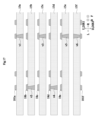
以下に、コイル部品11の製造方法について図面を参照しながら説明する。図3ないし図5は、コイル部品11の製造工程を示す断面図である。[Method for manufacturing coil component 11]
Below, a method for manufacturing the
まず、図3に示すように、樹脂層15b~15eのそれぞれにコイル導体18b~18e(第2コイル導体)を形成する(第2コイル導体形成工程)。具体的には、樹脂層15b~15eの上主面には金属箔が張り付けられている。この金属箔にマスクを形成する。そして、マスクを介してエッチングを施すことにより、コイル導体18b~18eを形成する。また、樹脂層15aの上主面及び樹脂層15fの下主面には金属膜200a,200bが設けられている。金属膜200a,200bは、金属箔に比べて薄い。 First, as shown in FIG. 3,
更に、樹脂層15a~15fに層間接続導体v1~v6を形成する。具体的には、樹脂層15a~15fのそれぞれにレーザービームを照射して貫通孔を形成する。その後、貫通孔に導電性ペーストを充填する。 Furthermore, interlayer connection conductors v1 to v6 are formed in the resin layers 15a to 15f. Specifically, through holes are formed by irradiating each of the resin layers 15a to 15f with a laser beam. After that, the through holes are filled with conductive paste.
図4に示すように、第2コイル導体形成工程の後に、樹脂層15a~15fを熱圧着する(熱圧着工程)。これにより、樹脂層15a~15fが軟化及び流動化する。そして、樹脂層15a~15fが冷却されると、樹脂層15a~15fが一体化される。更に、熱圧着により、貫通孔内の導電性ペーストが固化する。 As shown in FIG. 4, after the second coil conductor forming step, the resin layers 15a to 15f are thermocompression bonded (thermocompression bonding step). This softens and fluidizes the resin layers 15a to 15f. Then, when the resin layers 15a to 15f are cooled, the resin layers 15a to 15f are integrated. Furthermore, the conductive paste in the through hole is solidified by thermocompression bonding.
図5に示すように、熱圧着工程の後に、熱圧着工程において熱圧着した複数の樹脂層15a~15fの中で最も上(第1方向DIR1)に位置する樹脂層15aに位置するコイル導体18a(第1コイル導体)の上下方向の厚みを大きくする(第1コイル導体形成工程)。更に、熱圧着工程の後に、熱圧着工程において熱圧着した複数の樹脂層15a~15fの中で最も下(第2方向DIR2)に位置する樹脂層15fに位置するコイル導体18f(第3コイル導体)の上下方向の厚みを大きくする(第3コイル導体形成工程)。これにより、コイル導体18a,18fが完成する。コイル導体18a,18fは、例えば、MSAP(Modified Semi Additive Process)により形成される。MSAPでは、金属膜200a,200bの上にマスクを形成する。そして、金属膜200a,200bの上にメッキを施すことにより、メッキ層を形成する。その後、マスクを除去する。更に、エッチングにより、マスクと重なっていた不要な金属膜200a,200bを除去する。 As shown in FIG. 5, after the thermocompression bonding process, a
最後に、樹脂層15aの上主面に保護層16aを形成する。樹脂層15fの下主面に保護層16bを形成する。これにより、コイル部品11が完成する。 Finally, a
[効果]
コイル部品11によれば、コイル導体18a~18fの位置が設計値からずれることを抑制できると共に、コイルLの直流抵抗値を低減できる。より詳細には、コイルLの直流抵抗値を低減するためには、例えば、コイル導体18a~18fの上下方向の厚みを大きくすればよい。これにより、コイル導体18a~18fの断面積が大きくなり、コイル導体18a~18fの直流抵抗値が低減される。しかしながら、コイル導体18a~18fの上下方向の厚みが大きくなると、樹脂層15a~15fの熱圧着の際に、コイル導体18a~18fは、流動化した樹脂層15a~15fから前後方向及び左右方向に大きな力を受けやすい。その結果、コイル導体18a~18fの位置が設計値からずれてしまう。以上のように、コイル導体18a~18fの位置が設計値からずれることを抑制することと、コイルLの直流抵抗値を低減することとの両立は難しい。[effect]
According to the
そこで、本願発明者は、創意工夫の結果、以下の関係1及び関係3をコイル部品11に適用することに思い至った。 Therefore, as a result of ingenuity, the inventor of the present application came up with the idea of applying the following
関係1:コイル導体18a(第1コイル導体)の上下方向の厚みT1は、コイル導体18b~18e(第2コイル導体)の上下方向の厚みT2より大きい。
関係3:第1トップ部S2の線幅方向の幅W2を第1ボトム部S1の線幅方向の幅W1で割って得られる第1割合P1は、第2トップ部S4の線幅方向の幅W4を第2ボトム部S3の線幅方向の幅W3で割って得られる第2割合P2より小さい。Relationship 1: The vertical thickness T1 of the
Relationship 3: The first ratio P1 obtained by dividing the width W2 in the line width direction of the first top portion S2 by the width W1 in the line width direction of the first bottom portion S1 is the width in the line width direction of the second top portion S4. It is smaller than the second ratio P2 obtained by dividing W4 by the width W3 of the second bottom portion S3 in the line width direction.
関係1が成立することにより、コイル導体18aの断面積が大きくなるので、コイル導体18aの直流抵抗値が小さくなる。更に、関係1及び関係3が成立することにより、コイル導体18b~18eの位置が設計値からずれることが抑制される。より詳細には、コイル導体18b~18eは、熱圧着時に樹脂層15a~15fの内部に位置する。そのため、樹脂層15a~15fが流動化すると、コイル導体18c~18eの位置が設計値からずれやすい。そこで、関係1及び関係3が成立している。これにより、コイル導体18bの平坦性が向上する。より詳細には、関係1が成立することにより、コイル導体18bの上下方向の厚みT2が小さくなる。更に、関係3が成立することにより、コイル導体18bの第2トップ部S4が広くなる。このように、関係1及び関係3が成立することにより、コイル導体18bが扁平な断面形状を有するようになる。すなわち、コイル導体18bの平坦性が向上する。同じ理由により、コイル導体18c~18eの平坦性が向上する。このようにコイル導体18b~18eの平坦性が向上すると、コイル導体18b~18eは、熱圧着時に流動化した樹脂層15a~15fから前後方向及び左右方向に力を受けにくくなる。その結果、コイル導体18a~18fの位置が設計値からずれることが抑制される。 When
なお、関係2及び関係4が成立する場合も、関係1及び関係3が成立する場合と同じ理由により、コイル導体18a~18fの位置が設計値からずれることを抑制できると共に、コイルLの直流抵抗値を低減できる。 Note that even when
金属膜200a,200bは、金属箔に比べて薄い。これにより、MSAPにより、コイル導体18a,18fを形成する際に、エッチングにより、マスクと重なっていた不要な金属膜200a,200bを除去することが容易になる。 The
(第1変形例)
以下に、第1変形例に係るコイル部品11aについて図面を参照しながら説明する。図6は、コイル部品11aの断面図である。図7は、コイル部品11aの分解斜視図である。(First modification)
A
コイル部品11aは、コイル導体18a,18fの線幅方向の幅がコイル導体18b~18eの線幅方向の幅より大きい点においてコイル部品11と相違する。これにより、第1ボトム部S1の線幅方向の幅W1は、第2ボトム部S3の線幅方向の幅W3より大きい。第3ボトム部S5の線幅方向の幅W5は、第2ボトム部S3の線幅方向の幅W3より大きい。線幅方向に隣り合うコイル導体18a(第1コイル導体)同士の間隔d1は、線幅方向に隣り合うコイル導体18b~18e(第2コイル導体)同士の間隔d2より小さい。同様に、線幅方向に隣り合うコイル導体18f(第3コイル導体)同士の間隔d3は、線幅方向に隣り合うコイル導体18b~18e(第2コイル導体)同士の間隔d2より小さい。これにより、線幅方向に隣り合うコイル導体18b~18e(第2コイル導体)同士の間を樹脂層15a~15fが流動しやすくなる。その結果、線幅方向に隣り合うコイル導体18b~18e(第2コイル導体)同士の間に空孔が形成されることが抑制される。コイル部品11aのその他の構造は、コイル部品11と同じであるので説明を省略する。コイル部品11aは、コイル部品11と同じ作用効果を奏することができる。 The
(第2変形例)
以下に、第2変形例に係るコイル部品11bについて図面を参照しながら説明する。図8は、コイル部品11bの断面図である。図9は、コイル部品11bの分解斜視図である。(Second modification)
Below, a
コイル部品11bは、コイル導体18a,18fの形状においてコイル部品11と相違する。より詳細には、コイル導体18a,18fのそれぞれの周回数は、コイル導体18b~18eのそれぞれの周回数より多い。本実施形態では、コイル導体18a,18fのそれぞれの周回数は、コイル導体18b~18eのそれぞれの周回数の約2倍である。そして、コイル導体18a,18fの線幅方向の幅は、コイル導体18b~18eの線幅方向の幅より小さい。すなわち、第1ボトム部S1の線幅方向の幅W1は、第2ボトム部S3の線幅方向の幅W3より小さい。第3ボトム部S5の線幅方向の幅W5は、第2ボトム部S3の線幅方向の幅W3より小さい。そして、上下方向に見て、コイル導体18aの略全体は、コイル導体18b~18eと重なっている。同様に、コイル導体18fの略全体は、コイル導体18b~18eと重なっている。
また、コイル部品11bでは、以下の数式(1)及び数式(2)が成立する。 Further, in the
W1/T1×2<W3/T2 ・・・(1)
W5/T3×2<W3/T2 ・・・(2)
コイル部品11bのその他の構造は、コイル部品11と同じであるので説明を省略する。コイル部品11bは、コイル部品11と同じ作用効果を奏することができる。W1/T1×2<W3/T2...(1)
W5/T3×2<W3/T2...(2)
The other structure of the
また、コイル部品11bでは、コイル導体18a,18fのそれぞれの周回数は、コイル導体18b~18eのそれぞれの周回数より多い。これにより、コイルLのインダクタンス値が大きくなる。 Further, in the
(第3変形例)
以下に、第3変形例に係るコイル部品11cについて図面を参照しながら説明する。図10は、コイル部品11cの断面図である。(Third modification)
A
コイル部品11cは、線幅方向に隣り合うコイル導体18a同士の間隔が均一である点、及び、線幅方向に隣り合うコイル導体18f同士の間隔が均一である点においてコイル部品11bと相違する。コイル部品11cのその他の構造は、コイル部品11bと同じであるので説明を省略する。コイル部品11cは、コイル部品11bと同じ作用効果を奏することができる。 The
(第4変形例)
以下に、第4変形例に係るコイル部品11dについて図面を参照しながら説明する。図11は、コイル部品11dの断面図である。(Fourth modification)
A
コイル部品11dは、コイル導体18d~18fを備えていない点においてコイル部品11と相違する。コイル導体18b(第2コイル導体)は、樹脂層15aの下主面に位置している。そのため、コイル導体18bでは、第2ボトム部S3は、第2トップ部S4より上に位置している。そして、第2ボトム部S3は、樹脂層15aの下主面に固定されている。 The
また、コイル導体18a(第1コイル導体)の上下方向の厚みT1は、コイル導体18c(第3コイル導体)の上下方向の厚みT3より大きい。コイル導体18c(第3コイル導体)の外縁は、コイル導体18c(第3コイル導体)の外縁において最も下(第2方向)に位置する平面である第3ボトム部S5、及び、コイル導体18c(第3コイル導体)の外縁において最も上(第1方向)に位置する平面である第3トップ部S6を有している。第3トップ部S6は、第3ボトム部S5より上(第1方向DIR1)に位置し、第3ボトム部S5と平行な法線を有している。第3トップ部S6の線幅方向の幅W6は、第3ボトム部S5の線幅方向の幅W5より小さい。第1割合P1は、第3トップ部S6の線幅方向の幅W6を第3ボトム部S5の線幅方向の幅W5で割って得られる第3割合P3より小さい。 Further, the vertical thickness T1 of the
コイル部品11dのその他の構造は、コイル部品11と同じであるので説明を省略する。コイル部品11dは、コイル部品11と同じ作用効果を奏することができる。 The other structure of the
以下に、コイル部品11dの製造方法について図面を参照しながら説明する。図12ないし図14は、コイル部品11dの製造工程を示す断面図である。 Below, a method for manufacturing the
まず、図12に示すように、樹脂層15aにコイル導体18b(第2コイル導体)を形成する(第2コイル導体形成工程)。樹脂層15bにコイル導体18c(第3コイル導体)を形成する(第3コイル導体形成工程)。具体的には、樹脂層15aの上主面及び樹脂層15bの上主面のそれぞれには金属箔が張り付けられている。この金属箔にマスクを形成する。そして、マスクを介してエッチングを施すことにより、コイル導体18b,18cを形成する。また、樹脂層15aの上主面には金属膜200aが設けられている。金属膜200aは、金属箔に比べて薄い。 First, as shown in FIG. 12, a
更に、樹脂層15a,15bに層間接続導体v1,v2を形成する。具体的には、樹脂層15a,15bのそれぞれにレーザービームを照射して貫通孔を形成する。その後、貫通孔に導電性ペーストを充填する。 Furthermore, interlayer connection conductors v1 and v2 are formed on the resin layers 15a and 15b. Specifically, each of the resin layers 15a and 15b is irradiated with a laser beam to form a through hole. After that, the through holes are filled with conductive paste.
図13に示すように、第2コイル導体形成工程及び第3コイル導体形成工程の後に、コイル導体18b(第2コイル導体)及びコイル導体18c(第3コイル導体)が下方向(第2方向DIR2)にこの順に並ぶように樹脂層15a~15cを熱圧着する(熱圧着工程)。これにより、樹脂層15a~15cが軟化及び流動化する。そして、樹脂層15a~15cが冷却されると、樹脂層15a~15cが一体化される。更に、熱圧着により、貫通孔内の導電性ペーストが固化する。 As shown in FIG. 13, after the second coil conductor forming step and the third coil conductor forming step, the
図14に示すように、熱圧着工程の後に、熱圧着工程において熱圧着した複数の樹脂層15a~15cの中で最も上(第1方向DIR1)に位置する樹脂層15aに位置するコイル導体18a(第1コイル導体)の上下方向の厚みを大きくする(第1コイル導体形成工程)。コイル導体18aは、例えば、MSAPにより形成される。MSAPでは、金属膜200aの上にマスクを形成する。そして、金属膜200aの上にメッキを施すことにより、メッキ層を形成する。その後、マスクを除去する。更に、エッチングにより、マスクと重なっていた不要な金属膜200aを除去する。 As shown in FIG. 14, after the thermocompression bonding step, a
最後に、樹脂層15aの上主面に保護層16aを形成する。これにより、コイル部品11dが完成する。 Finally, a
(第5変形例)
以下に、第5変形例に係るコイル部品11eについて図面を参照しながら説明する。図15は、コイル部品11eの断面図である。(Fifth modification)
A
コイル部品11eは、樹脂層15g及び層間接続導体v11を更に備えている点及びコイル導体18b,18cの位置が異なる点においてコイル部品11dと相違する。より詳細には、樹脂層15gは、樹脂層15aと樹脂層15bとの間に位置している。コイル導体18bは、樹脂層15gの下主面に位置している。コイル導体18cは、樹脂層15bの下主面に位置している。そのため、コイル導体18bでは、第3ボトム部S5は、第3トップ部S6より上に位置している。そして、第3ボトム部S5は、樹脂層15gの下主面に固定されている。層間接続導体v11は、層間接続導体v1と直列に接続されている。層間接続導体v1,v11は、コイル導体18aの内周端部とコイル導体18bの内周端部とを電気的に接続している。コイル部品11eのその他の構造は、コイル部品11dと同じであるので説明を省略する。コイル部品11eは、コイル部品11dと同じ作用効果を奏することができる。 The
(第6変形例)
以下に、第6変形例に係るコイル部品11fについて図面を参照しながら説明する。図16は、コイル部品11fの断面図である。(Sixth variation)
A
コイル部品11fは、コイル導体18a,18fの構造においてコイル部品11と相違する。より詳細には、コイル部品11fでは、コイル導体18aは、ベース導体181a及びメッキ層182aを含んでいる。ベース導体181aは、金属箔により作製されている。メッキ層182aは、ベース導体181aを覆っている。コイル導体18fは、ベース導体181f及びメッキ層182fを含んでいる。ベース導体181fは、金属箔により作製されている。メッキ層182fは、ベース導体181fを覆っている。コイル部品11fのその他の構造は、コイル部品11と同じであるので説明を省略する。コイル部品11fは、コイル部品11と同じ作用効果を奏することができる。 The
また、コイル部品11fでは、上下方向に見て、コイル導体18aの略全体は、コイル導体18b~18eと重なっている。同様に、コイル導体18fの略全体は、コイル導体18b~18eと重なっている。これにより、樹脂層15a~15fの熱圧着時に、コイル導体18a~18fに上下方向に力が加わりやすくなり、コイル導体18a~18fに前後方向及び左右方向に力が加わりにくくなる。その結果、コイル導体18a~18fの位置が設計値からずれることが抑制される。 Further, in the
次に、コイル部品11fの製造方法について図面を参照しながら説明する。図17ないし図19は、コイル部品11fの製造工程を示す断面図である。 Next, a method for manufacturing the
まず、図17に示すように、樹脂層15b~15eのそれぞれにコイル導体18b~18e(第2コイル導体)を形成する(第2コイル導体形成工程)。具体的には、樹脂層15a~15fの上主面には金属箔が張り付けられている。この金属箔にマスクを形成する。そして、マスクを介してエッチングを施すことにより、コイル導体18b~18eを形成する。 First, as shown in FIG. 17,
また、樹脂層15aの上主面及び樹脂層15fの下主面のそれぞれにベース導体181a,181fを形成する。具体的には、樹脂層15aの上主面及び樹脂層15fの下主面のそれぞれには金属箔が張り付けられている。この金属箔にマスクを形成する。そして、マスクを介してエッチングを施すことにより、ベース導体181a,181fを形成する。 Further,
更に、樹脂層15b~15eに層間接続導体v1~v6を形成する。具体的には、樹脂層15b~15eのそれぞれにレーザービームを照射して貫通孔を形成する。その後、貫通孔に導電性ペーストを充填する。 Further, interlayer connection conductors v1 to v6 are formed in the resin layers 15b to 15e. Specifically, each of the resin layers 15b to 15e is irradiated with a laser beam to form a through hole. After that, the through holes are filled with conductive paste.
図18に示すように、樹脂層15a~15fを熱圧着する(熱圧着工程)。これにより、樹脂層15a~15fが軟化及び流動化する。そして、樹脂層15a~15fが冷却されると、樹脂層15a~15fが一体化される。更に、熱圧着により、貫通孔内の導電性ペーストが固化する。 As shown in FIG. 18, the resin layers 15a to 15f are thermocompression bonded (thermocompression bonding step). This softens and fluidizes the resin layers 15a to 15f. Then, when the resin layers 15a to 15f are cooled, the resin layers 15a to 15f are integrated. Furthermore, the conductive paste in the through hole is solidified by thermocompression bonding.
図19に示すように、熱圧着工程において熱圧着した複数の樹脂層15a~15fの中で最も上(第1方向DIR1)に位置する樹脂層15aに位置するコイル導体18a(第1コイル導体)の上下方向の厚みを大きくする(第1コイル導体形成工程)。更に、熱圧着工程の後に、熱圧着工程において熱圧着した複数の樹脂層15a~15fの中で最も下(第2方向DIR2)に位置する樹脂層15fに位置するコイル導体18f(第3コイル導体)の厚みを大きくする(第3コイル導体形成工程)。具体的には、ベース導体181a,181fのそれぞれにメッキを施すことにより、メッキ層182a,182fを完成させる。 As shown in FIG. 19, a
最後に、樹脂層15aの上主面に保護層16aを形成する。樹脂層15fの下主面に保護層16bを形成する。これにより、コイル部品11fが完成する。 Finally, a
(第7変形例)
以下に、第7変形例に係るコイル部品11gについて図面を参照しながら説明する。図20は、コイル部品11gの断面図である。(Seventh modification)
Below, a
コイル部品11gは、コイル部品11h,11iを含んでいる。コイル部品11h,11iのそれぞれは、コイル部品11と同じ構造を有している。コイル部品11hは、コイル部品11iの上主面に実装されている。これにより、コイル部品11hのコイル導体18fとコイル部品11iのコイル導体18aとが半田により電気的に接続されている。 The
これにより、コイル部品11gは、コイル部品11hのコイルL1とコイル部品11iのコイルL2とが直列に接続された構造を有するようになる。その結果、コイル部品11gでは、コイルLのインダクタンス値が大きくなる。 Thereby, the
(その他の実施形態)
本発明に係るコイル部品は、コイル部品11,11a~11gに限らず、その要旨の範囲内において変更可能である。なお、コイル部品11,11a~11gの構成を任意に組み合わせてもよい。(Other embodiments)
The coil components according to the present invention are not limited to the
なお、コイルLは、複数の渦巻状のコイル導体が接続された構造を有している。しかしながら、コイルLが螺旋形状を有していれば、複数のコイル導体の周回数は1周以下であってもよい。 Note that the coil L has a structure in which a plurality of spiral coil conductors are connected. However, as long as the coil L has a spiral shape, the number of turns of the plurality of coil conductors may be one turn or less.
なお、駆動モジュール10において、磁石50の左部がS極であり、磁石50の右部がN極であってもよい。なお、磁石50は、永久磁石であってもよいし、電磁石であってもよい。 In addition, in the
なお、樹脂層15a~15fの材料は、磁性体材料であってもよい。 Note that the material of the resin layers 15a to 15f may be a magnetic material.
なお、樹脂層15a~15fの材料は、熱可塑性樹脂以外の樹脂であってもよい。 Note that the material of the resin layers 15a to 15f may be a resin other than thermoplastic resin.
なお、樹脂層15aの上に更に樹脂層が積層されてもよい。樹脂層15fの下に更に樹脂層が積層されてもよい。 Note that a resin layer may be further laminated on the
なお、下方向が第1方向DIR1であり、上方向が第2方向DIR2であってもよい。 Note that the downward direction may be the first direction DIR1, and the upward direction may be the second direction DIR2.
なお、第1ボトム部S1の線幅方向の幅W1は、第2ボトム部S3の線幅方向の幅W3以上であってもよい。 Note that the width W1 of the first bottom portion S1 in the line width direction may be greater than or equal to the width W3 of the second bottom portion S3 in the line width direction.
なお、線幅方向に隣り合うコイル導体18a(第1コイル導体)同士の間隔は、線幅方向に隣り合うコイル導体18b~18e(第2コイル導体)同士の間隔以上であってもよい。 Note that the distance between the
なお、コイル部品11,11a~11c,11f,11gにおいて、第3割合P3は、第2割合P2以上であってもよい。 Note that in the
なお、コイル部品11,11a~11c,11f,11gにおいて、第3ボトム部S5の線幅方向の幅W5は、第2ボトム部S3の線幅方向の幅W3以上であってもよい。 Note that in the
なお、コイル部品11,11a~11c,11f,11gにおいて、線幅方向に隣り合うコイル導体18f(第3コイル導体)同士の間隔は、線幅方向に隣り合うコイル導体18b~18e(第2コイル導体)同士の間隔以上であってもよい。 In the
なお、コイル部品11d,11eにおいて、第1割合P1は、第3割合P3以上であってもよい。 Note that in the
なお、コイル部品11,11a~11fは、駆動モジュールに適用されている。しかしながら、コイル部品11,11a~11fは、駆動モジュール以外の用途に用いられてもよい。コイル部品11,11a~11fは、例えば、アンテナ素子として用いられてもよい。この場合、コイルLは、通信用のアンテナ又はワイヤレス給電用のアンテナとして機能する。 Note that the
10:駆動モジュール
11,11a~11i:コイル部品
12:積層体
15a~15f:樹脂層
16a,16b:保護層
18a~18f:コイル導体
20a,20b:引き出し導体
50:磁石
181a,181f:ベース導体
182a,182f:メッキ層
Ax1:中心軸線
L:コイル
L1:コイル
L2:コイル
S1:第1ボトム部
S2:第1トップ部
S3:第2ボトム部
S4:第2トップ部
S5:第3ボトム部
S6:第3トップ部
v1~v6:層間接続導体10:
Claims (11)
複数の樹脂層が上下方向に積層された構造を有する積層体と、
上下方向に見て線形状を有する複数のコイル導体を含んでいるコイルであって、上下方向に延びる中心軸線の周囲を周回する螺旋形状を有しているコイルであって、前記複数のコイル導体は、前記第2方向にこの順に並ぶ第1コイル導体、第2コイル導体及び第3コイル導体を含んでいる、コイルと、
を備えており、
前記第1コイル導体は、前記複数のコイル導体の中で最も前記第1方向に位置しており、
上下方向に見て、前記第1コイル導体、前記第2コイル導体及び前記第3コイル導体のそれぞれが延びる方向に直交する方向は、線幅方向であり、
前記第1コイル導体の外縁は、前記第1コイル導体の外縁において最も前記第2方向に位置する平面である第1ボトム部、及び、前記第1コイル導体の外縁において最も前記第1方向に位置する平面である第1トップ部を有しており、
前記第1トップ部の前記線幅方向の幅は、前記第1ボトム部の前記線幅方向の幅より小さく、
前記第2コイル導体の外縁は、前記第1コイル導体の外縁において最も前記第2方向に位置する平面である第2ボトム部、及び、前記第2コイル導体の外縁において最も前記第1方向に位置する平面である第2トップ部を有しており、
前記第2トップ部の前記線幅方向の幅は、前記第2ボトム部の前記線幅方向の幅より小さく、
前記第1トップ部と前記第1ボトム部との最短距離は、前記第2トップ部と前記第2ボトム部との最短距離より長く、
前記第1トップ部の前記線幅方向の幅を前記第1ボトム部の前記線幅方向の幅で割って得られる第1割合は、前記第2トップ部の前記線幅方向の幅を前記第2ボトム部の前記線幅方向の幅で割って得られる第2割合より小さい、
コイル部品。 One direction in the vertical direction is a first direction, the other direction in the vertical direction is a second direction,
A laminate having a structure in which a plurality of resin layers are stacked in the vertical direction;
A coil including a plurality of coil conductors having a linear shape when viewed in the vertical direction, the coil having a spiral shape circulating around a central axis extending in the vertical direction, the plurality of coil conductors a coil including a first coil conductor, a second coil conductor, and a third coil conductor arranged in this order in the second direction;
It is equipped with
The first coil conductor is located furthest in the first direction among the plurality of coil conductors,
When viewed in the vertical direction, the direction perpendicular to the direction in which each of the first coil conductor, the second coil conductor, and the third coil conductor extends is a line width direction,
The outer edge of the first coil conductor includes a first bottom portion which is a plane located furthest in the second direction at the outer edge of the first coil conductor, and a first bottom portion which is a plane located furthest in the first direction at the outer edge of the first coil conductor. has a first top portion that is a flat surface,
The width of the first top portion in the line width direction is smaller than the width of the first bottom portion in the line width direction,
The outer edge of the second coil conductor includes a second bottom portion which is a plane located furthest in the second direction at the outer edge of the first coil conductor, and a second bottom portion which is a plane located furthest in the first direction at the outer edge of the second coil conductor. It has a second top part that is a flat surface,
The width of the second top portion in the line width direction is smaller than the width of the second bottom portion in the line width direction,
The shortest distance between the first top part and the first bottom part is longer than the shortest distance between the second top part and the second bottom part,
A first ratio obtained by dividing the width of the first top portion in the line width direction by the width of the first bottom portion in the line width direction is calculated by dividing the width of the second top portion in the line width direction by the width of the second top portion in the line width direction. 2 smaller than a second ratio obtained by dividing by the width in the line width direction of the bottom portion;
coil parts.
請求項1に記載のコイル部品。 The width of the first bottom portion in the line width direction is smaller than the width of the second bottom portion in the line width direction.
The coil component according to claim 1.
請求項1に記載のコイル部品。 The width of the first bottom portion in the line width direction is larger than the width of the second bottom portion in the line width direction.
The coil component according to claim 1.
前記線幅方向に隣り合う前記第1コイル導体同士の間隔は、前記線幅方向に隣り合う前記第2コイル導体同士の間隔より小さい、
請求項1ないし請求項3のいずれかに記載のコイル部品。 Each of the first coil conductor, the second coil conductor, and the third coil conductor has a spiral shape that revolves around the central axis for one or more turns when viewed in the vertical direction,
The distance between the first coil conductors adjacent to each other in the line width direction is smaller than the distance between the second coil conductors adjacent to each other in the line width direction.
The coil component according to any one of claims 1 to 3.
前記第3コイル導体の外縁は、前記第3コイル導体の外縁において最も前記第2方向に位置する平面である第3ボトム部、及び、前記第3コイル導体の外縁において最も前記第1方向に位置する平面である第3トップ部を有しており、
前記第3トップ部の前記線幅方向の幅は、前記第3ボトム部の前記線幅方向の幅より小さく、
前記第3トップ部と前記第3ボトム部との最短距離は、前記第2トップ部と前記第2ボトム部との最短距離より長く、
前記第3トップ部の前記線幅方向の幅を前記第3ボトム部の前記線幅方向の幅で割って得られる第3割合は、前記第2割合より小さい、
請求項1ないし請求項3のいずれかに記載のコイル部品。 The third coil conductor is located furthest in the second direction among the plurality of coil conductors,
The outer edge of the third coil conductor includes a third bottom portion which is a plane located furthest in the second direction at the outer edge of the third coil conductor, and a third bottom portion which is a plane located furthest in the first direction at the outer edge of the third coil conductor. It has a third top part that is a flat surface,
The width of the third top portion in the line width direction is smaller than the width of the third bottom portion in the line width direction,
The shortest distance between the third top part and the third bottom part is longer than the shortest distance between the second top part and the second bottom part,
A third ratio obtained by dividing the width of the third top portion in the line width direction by the width of the third bottom portion in the line width direction is smaller than the second ratio.
The coil component according to any one of claims 1 to 3 .
請求項5に記載のコイル部品。 The width of the third bottom portion in the line width direction is smaller than the width of the second bottom portion in the line width direction.
The coil component according to claim 5.
請求項5に記載のコイル部品。 The width of the third bottom portion in the line width direction is larger than the width of the second bottom portion in the line width direction.
The coil component according to claim 5.
前記線幅方向に隣り合う前記第3コイル導体同士の間隔は、前記線幅方向に隣り合う前記第2コイル導体同士の間隔より小さい、
請求項5に記載のコイル部品。 The first coil conductor, the second coil conductor, and the third coil conductor have a spiral shape that revolves around the central axis for one or more turns when viewed in the vertical direction,
The distance between the third coil conductors adjacent to each other in the line width direction is smaller than the distance between the second coil conductors adjacent to each other in the line width direction.
The coil component according to claim 5.
前記第3トップ部の前記線幅方向の幅は、前記第3ボトム部の前記線幅方向の幅より小さく、
前記第1トップ部と前記第1ボトム部との最短距離は、前記第3トップ部と前記第3ボトム部との最短距離より長く、
前記第1割合は、前記第3トップ部の前記線幅方向の幅を前記第3ボトム部の前記線幅方向の幅で割って得られる第3割合より小さい、
請求項1ないし請求項3のいずれかに記載のコイル部品。 The outer edge of the third coil conductor includes a third bottom portion which is a plane located furthest in the second direction at the outer edge of the third coil conductor, and a third bottom portion which is a plane located furthest in the first direction at the outer edge of the third coil conductor. It has a third top part that is a flat surface,
The width of the third top portion in the line width direction is smaller than the width of the third bottom portion in the line width direction,
The shortest distance between the first top part and the first bottom part is longer than the shortest distance between the third top part and the third bottom part,
The first ratio is smaller than a third ratio obtained by dividing the width of the third top part in the line width direction by the width of the third bottom part in the line width direction.
The coil component according to any one of claims 1 to 3 .
複数の樹脂層が上下方向に積層された構造を有する積層体と、
上下方向に見て線形状を有する複数のコイル導体を含んでいるコイルであって、上下方向に延びる中心軸線の周囲を周回する螺旋形状を有しているコイルであって、前記複数のコイル導体は、前記第2方向にこの順に並ぶ第1コイル導体、第2コイル導体及び第3コイル導体を含んでいる、コイルと、
を備える、
コイル部品の製造方法であって、
前記樹脂層に前記第2コイル導体を形成する第2コイル導体形成工程と、
前記第2コイル導体形成工程の後に、前記複数の樹脂層を熱圧着する熱圧着工程と、
前記熱圧着工程の後に、前記熱圧着工程において熱圧着した前記複数の樹脂層の中で最も前記第1方向に位置する前記樹脂層に位置する前記第1コイル導体の上下方向の厚みを大きくする第1コイル導体形成工程と、
前記熱圧着工程の後に、前記熱圧着工程において熱圧着した前記複数の樹脂層の中で最も前記第2方向に位置する前記樹脂層に位置する前記第3コイル導体の上下方向の厚みを大きくする第3コイル導体形成工程と、
を備えており、
上下方向に見て、前記第1コイル導体、前記第2コイル導体及び前記第3コイル導体のそれぞれが延びる方向に直交する方向は、線幅方向であり、
前記第1コイル導体の外縁は、前記第1コイル導体の外縁において最も前記第2方向に位置する平面である第1ボトム部、及び、前記第1コイル導体の外縁において最も前記第1方向に位置する平面である第1トップ部を有しており、
前記第1トップ部の前記線幅方向の幅は、前記第1ボトム部の前記線幅方向の幅より小さく、
前記第2コイル導体の外縁は、前記第2コイル導体の外縁において最も前記第2方向に位置する平面である第2ボトム部、及び、前記第2コイル導体の外縁において最も前記第1方向に位置する平面である第2トップ部を有しており、
前記第2トップ部の前記線幅方向の幅は、前記第2ボトム部の前記線幅方向の幅より小さく、
前記第1トップ部と前記第1ボトム部との最短距離は、前記第2トップ部と前記第2ボトム部との最短距離より長く、
前記第1トップ部の前記線幅方向の幅を前記第1ボトム部の前記線幅方向の幅で割って得られる第1割合は、前記第2トップ部の前記線幅方向の幅を前記第2ボトム部の前記線幅方向の幅で割って得られる第2割合より小さい、
コイル部品の製造方法。 One direction in the vertical direction is a first direction, the other direction in the vertical direction is a second direction,
A laminate having a structure in which a plurality of resin layers are stacked in the vertical direction;
A coil including a plurality of coil conductors having a linear shape when viewed in the vertical direction, the coil having a spiral shape circulating around a central axis extending in the vertical direction, the plurality of coil conductors a coil including a first coil conductor, a second coil conductor, and a third coil conductor arranged in this order in the second direction;
Equipped with
A method for manufacturing a coil component,
a second coil conductor forming step of forming the second coil conductor on the resin layer;
a thermocompression bonding step of thermocompression bonding the plurality of resin layers after the second coil conductor forming step;
After the thermocompression bonding step, the vertical thickness of the first coil conductor located in the resin layer located in the first direction among the plurality of resin layers thermocompression bonded in the thermocompression bonding step is increased. A first coil conductor forming step;
After the thermocompression bonding step, the thickness in the vertical direction of the third coil conductor located in the resin layer located in the second direction most among the plurality of resin layers thermocompression bonded in the thermocompression bonding step is increased. A third coil conductor forming step,
It is equipped with
When viewed in the vertical direction, the direction perpendicular to the direction in which each of the first coil conductor, the second coil conductor, and the third coil conductor extends is a line width direction,
The outer edge of the first coil conductor includes a first bottom portion which is a plane located furthest in the second direction at the outer edge of the first coil conductor, and a first bottom portion which is a plane located furthest in the first direction at the outer edge of the first coil conductor. has a first top portion that is a flat surface,
The width of the first top portion in the line width direction is smaller than the width of the first bottom portion in the line width direction,
The outer edge of the second coil conductor includes a second bottom portion which is a plane located furthest in the second direction at the outer edge of the second coil conductor, and a second bottom portion which is a plane located furthest in the first direction at the outer edge of the second coil conductor. It has a second top part that is a flat surface,
The width of the second top portion in the line width direction is smaller than the width of the second bottom portion in the line width direction,
The shortest distance between the first top part and the first bottom part is longer than the shortest distance between the second top part and the second bottom part,
A first ratio obtained by dividing the width of the first top portion in the line width direction by the width of the first bottom portion in the line width direction is calculated by dividing the width of the second top portion in the line width direction by the width of the second top portion in the line width direction. 2 smaller than a second ratio obtained by dividing by the width in the line width direction of the bottom portion;
Method of manufacturing coil parts.
複数の樹脂層が上下方向に積層された構造を有する積層体と、
上下方向に見て線形状を有する複数のコイル導体を含んでいるコイルであって、上下方向に延びる中心軸線の周囲を周回する螺旋形状を有しているコイルであって、前記複数のコイル導体は、前記第2方向にこの順に並ぶ第1コイル導体、第2コイル導体及び第3コイル導体を含んでいる、コイルと、
を備える、
コイル部品の製造方法であって、
前記樹脂層に前記第2コイル導体を形成する第2コイル導体形成工程と、
前記樹脂層に前記第3コイル導体を形成する第3コイル導体形成工程と、
前記第2コイル導体形成工程及び前記第3コイル導体形成工程の後に、前記第2コイル導体及び前記第3コイル導体が前記第2方向にこの順に並ぶように前記複数の樹脂層を熱圧着する熱圧着工程と、
前記熱圧着工程の後に、前記熱圧着工程において熱圧着した前記複数の樹脂層の中で最も前記第1方向に位置する前記樹脂層に位置する前記第1コイル導体の上下方向の厚みを大きくする第1コイル導体形成工程と、
を備えており、
上下方向に見て、前記第1コイル導体、前記第2コイル導体及び前記第3コイル導体のそれぞれが延びる方向に直交する方向は、線幅方向であり、
前記第1コイル導体の外縁は、前記第1コイル導体の外縁において最も前記第2方向に位置する平面である第1ボトム部、及び、前記第1コイル導体の外縁において最も前記第1方向に位置する平面である第1トップ部を有しており、
前記第1トップ部の前記線幅方向の幅は、前記第1ボトム部の前記線幅方向の幅より小さく、
前記第2コイル導体の外縁は、前記第2コイル導体の外縁において最も前記第2方向に位置する平面である第2ボトム部、及び、前記第2コイル導体の外縁において最も前記第1方向に位置する平面である第2トップ部を有しており、
前記第2トップ部の前記線幅方向の幅は、前記第2ボトム部の前記線幅方向の幅より小さく、
前記第1トップ部と前記第1ボトム部との最短距離は、前記第2トップ部と前記第2ボトム部との最短距離より長く、
前記第1トップ部の前記線幅方向の幅を前記第1ボトム部の前記線幅方向の幅で割って得られる第1割合は、前記第2トップ部の前記線幅方向の幅を前記第2ボトム部の前記線幅方向の幅で割って得られる第2割合より小さい、
コイル部品の製造方法。 One direction in the vertical direction is a first direction, the other direction in the vertical direction is a second direction,
A laminate having a structure in which a plurality of resin layers are stacked in the vertical direction;
A coil including a plurality of coil conductors having a linear shape when viewed in the vertical direction, the coil having a spiral shape circulating around a central axis extending in the vertical direction, the plurality of coil conductors a coil including a first coil conductor, a second coil conductor, and a third coil conductor arranged in this order in the second direction;
Equipped with
A method for manufacturing a coil component,
a second coil conductor forming step of forming the second coil conductor on the resin layer;
a third coil conductor forming step of forming the third coil conductor on the resin layer;
After the second coil conductor forming step and the third coil conductor forming step, heat-bonding the plurality of resin layers by thermocompression so that the second coil conductor and the third coil conductor are lined up in this order in the second direction. crimping process,
After the thermocompression bonding step, the vertical thickness of the first coil conductor located in the resin layer located in the first direction among the plurality of resin layers thermocompression bonded in the thermocompression bonding step is increased. A first coil conductor forming step;
It is equipped with
When viewed in the vertical direction, the direction perpendicular to the direction in which each of the first coil conductor, the second coil conductor, and the third coil conductor extends is a line width direction,
The outer edge of the first coil conductor includes a first bottom portion which is a plane located furthest in the second direction at the outer edge of the first coil conductor, and a first bottom portion which is a plane located furthest in the first direction at the outer edge of the first coil conductor. has a first top portion that is a flat surface,
The width of the first top portion in the line width direction is smaller than the width of the first bottom portion in the line width direction,
The outer edge of the second coil conductor includes a second bottom portion which is a plane located furthest in the second direction at the outer edge of the second coil conductor, and a second bottom portion which is a plane located furthest in the first direction at the outer edge of the second coil conductor. It has a second top part that is a flat surface,
The width of the second top portion in the line width direction is smaller than the width of the second bottom portion in the line width direction,
The shortest distance between the first top part and the first bottom part is longer than the shortest distance between the second top part and the second bottom part,
A first ratio obtained by dividing the width of the first top portion in the line width direction by the width of the first bottom portion in the line width direction is calculated by dividing the width of the second top portion in the line width direction by the width of the first bottom portion in the line width direction. 2 smaller than a second ratio obtained by dividing by the width in the line width direction of the bottom portion;
Method of manufacturing coil parts.
Applications Claiming Priority (3)
| Application Number | Priority Date | Filing Date | Title |
|---|---|---|---|
| JP2021132218 | 2021-08-16 | ||
| JP2021132218 | 2021-08-16 | ||
| PCT/JP2022/028172 WO2023021909A1 (en) | 2021-08-16 | 2022-07-20 | Coil component and method for manufacturing coil component |
Publications (3)
| Publication Number | Publication Date |
|---|---|
| JPWO2023021909A1 JPWO2023021909A1 (en) | 2023-02-23 |
| JPWO2023021909A5 JPWO2023021909A5 (en) | 2023-09-13 |
| JP7351441B2 true JP7351441B2 (en) | 2023-09-27 |
Family
ID=85240490
Family Applications (1)
| Application Number | Title | Priority Date | Filing Date |
|---|---|---|---|
| JP2023540834A Active JP7351441B2 (en) | 2021-08-16 | 2022-07-20 | Coil parts and method for manufacturing coil parts |
Country Status (3)
| Country | Link |
|---|---|
| JP (1) | JP7351441B2 (en) |
| CN (1) | CN220252959U (en) |
| WO (1) | WO2023021909A1 (en) |
Family Cites Families (3)
| Publication number | Priority date | Publication date | Assignee | Title |
|---|---|---|---|---|
| JP6520604B2 (en) * | 2015-09-18 | 2019-05-29 | Tdk株式会社 | Laminated coil parts |
| JP6658681B2 (en) * | 2017-06-22 | 2020-03-04 | 株式会社村田製作所 | Manufacturing method of multilayer inductor and multilayer inductor |
| JP2020013826A (en) * | 2018-07-13 | 2020-01-23 | イビデン株式会社 | Coil substrate |
-
2022
- 2022-07-20 CN CN202290000247.1U patent/CN220252959U/en active Active
- 2022-07-20 JP JP2023540834A patent/JP7351441B2/en active Active
- 2022-07-20 WO PCT/JP2022/028172 patent/WO2023021909A1/en active Application Filing
Also Published As
| Publication number | Publication date |
|---|---|
| CN220252959U (en) | 2023-12-26 |
| JPWO2023021909A1 (en) | 2023-02-23 |
| WO2023021909A1 (en) | 2023-02-23 |
Similar Documents
| Publication | Publication Date | Title |
|---|---|---|
| US9349522B2 (en) | Coil component | |
| JP6024243B2 (en) | Coil component and manufacturing method thereof | |
| US6848178B2 (en) | Enhancement of current-carrying capacity of a multilayer circuit board | |
| US9504142B2 (en) | Flexible flat circuit | |
| JP6030512B2 (en) | Multilayer electronic components | |
| US9934905B2 (en) | Method of manufacturing multilayer board, multilayer board, and electromagnet | |
| JP2013051336A (en) | Wiring board with built-in component, and manufacturing method therefor | |
| US10388451B2 (en) | Inductor component and method for manufacturing inductor component | |
| US20170110234A1 (en) | Coil component, manufacturing method thereof, and circuit board on which coil component are mounted | |
| US10804784B2 (en) | Actuator | |
| KR101989261B1 (en) | Stacked electronic component | |
| JP6828568B2 (en) | Coil parts | |
| KR20140108873A (en) | Power inductor and manufacturing method thereof | |
| CN112908611B (en) | Coil component | |
| CN209949596U (en) | Multilayer substrate | |
| JP6436126B2 (en) | Electronic component and method for manufacturing electronic component | |
| JP2017017140A (en) | Coil component | |
| CN105609231A (en) | Laminated inductor and manufacturing method therefor and lamination packaging assembly | |
| JP7351441B2 (en) | Coil parts and method for manufacturing coil parts | |
| WO2014155952A1 (en) | Layered inductor | |
| JP7489521B2 (en) | Rigid-flex multilayer printed wiring boards | |
| JP4064049B2 (en) | Manufacturing method of multilayer electronic component | |
| JPWO2017199747A1 (en) | Multilayer substrate and method of manufacturing multilayer substrate | |
| JP7351440B2 (en) | Substrate module, drive module and electronic equipment | |
| US20230317358A1 (en) | Coil component |
Legal Events
| Date | Code | Title | Description |
|---|---|---|---|
| A521 | Request for written amendment filed |
Free format text: JAPANESE INTERMEDIATE CODE: A523 Effective date: 20230703 |
|
| A621 | Written request for application examination |
Free format text: JAPANESE INTERMEDIATE CODE: A621 Effective date: 20230703 |
|
| A871 | Explanation of circumstances concerning accelerated examination |
Free format text: JAPANESE INTERMEDIATE CODE: A871 Effective date: 20230703 |
|
| TRDD | Decision of grant or rejection written | ||
| A01 | Written decision to grant a patent or to grant a registration (utility model) |
Free format text: JAPANESE INTERMEDIATE CODE: A01 Effective date: 20230815 |
|
| A61 | First payment of annual fees (during grant procedure) |
Free format text: JAPANESE INTERMEDIATE CODE: A61 Effective date: 20230828 |
|
| R150 | Certificate of patent or registration of utility model |
Ref document number: 7351441 Country of ref document: JP Free format text: JAPANESE INTERMEDIATE CODE: R150 |