JP7345572B2 - Methods for measuring and correcting misalignment between layers in semiconductor devices, and misalignment targets useful therein - Google Patents
Methods for measuring and correcting misalignment between layers in semiconductor devices, and misalignment targets useful therein Download PDFInfo
- Publication number
- JP7345572B2 JP7345572B2 JP2021576144A JP2021576144A JP7345572B2 JP 7345572 B2 JP7345572 B2 JP 7345572B2 JP 2021576144 A JP2021576144 A JP 2021576144A JP 2021576144 A JP2021576144 A JP 2021576144A JP 7345572 B2 JP7345572 B2 JP 7345572B2
- Authority
- JP
- Japan
- Prior art keywords
- misalignment
- semiconductor device
- indication
- post
- measurement
- Prior art date
- Legal status (The legal status is an assumption and is not a legal conclusion. Google has not performed a legal analysis and makes no representation as to the accuracy of the status listed.)
- Active
Links
Images


Classifications
-
- H—ELECTRICITY
- H01—ELECTRIC ELEMENTS
- H01L—SEMICONDUCTOR DEVICES NOT COVERED BY CLASS H10
- H01L21/00—Processes or apparatus adapted for the manufacture or treatment of semiconductor or solid state devices or of parts thereof
- H01L21/67—Apparatus specially adapted for handling semiconductor or electric solid state devices during manufacture or treatment thereof; Apparatus specially adapted for handling wafers during manufacture or treatment of semiconductor or electric solid state devices or components ; Apparatus not specifically provided for elsewhere
- H01L21/67005—Apparatus not specifically provided for elsewhere
- H01L21/67242—Apparatus for monitoring, sorting or marking
- H01L21/67276—Production flow monitoring, e.g. for increasing throughput
-
- G—PHYSICS
- G03—PHOTOGRAPHY; CINEMATOGRAPHY; ANALOGOUS TECHNIQUES USING WAVES OTHER THAN OPTICAL WAVES; ELECTROGRAPHY; HOLOGRAPHY
- G03F—PHOTOMECHANICAL PRODUCTION OF TEXTURED OR PATTERNED SURFACES, e.g. FOR PRINTING, FOR PROCESSING OF SEMICONDUCTOR DEVICES; MATERIALS THEREFOR; ORIGINALS THEREFOR; APPARATUS SPECIALLY ADAPTED THEREFOR
- G03F7/00—Photomechanical, e.g. photolithographic, production of textured or patterned surfaces, e.g. printing surfaces; Materials therefor, e.g. comprising photoresists; Apparatus specially adapted therefor
- G03F7/70—Microphotolithographic exposure; Apparatus therefor
- G03F7/70483—Information management; Active and passive control; Testing; Wafer monitoring, e.g. pattern monitoring
- G03F7/70605—Workpiece metrology
- G03F7/70616—Monitoring the printed patterns
- G03F7/70633—Overlay, i.e. relative alignment between patterns printed by separate exposures in different layers, or in the same layer in multiple exposures or stitching
-
- G—PHYSICS
- G05—CONTROLLING; REGULATING
- G05B—CONTROL OR REGULATING SYSTEMS IN GENERAL; FUNCTIONAL ELEMENTS OF SUCH SYSTEMS; MONITORING OR TESTING ARRANGEMENTS FOR SUCH SYSTEMS OR ELEMENTS
- G05B19/00—Programme-control systems
- G05B19/02—Programme-control systems electric
- G05B19/418—Total factory control, i.e. centrally controlling a plurality of machines, e.g. direct or distributed numerical control [DNC], flexible manufacturing systems [FMS], integrated manufacturing systems [IMS], computer integrated manufacturing [CIM]
- G05B19/41875—Total factory control, i.e. centrally controlling a plurality of machines, e.g. direct or distributed numerical control [DNC], flexible manufacturing systems [FMS], integrated manufacturing systems [IMS], computer integrated manufacturing [CIM] characterised by quality surveillance of production
-
- H—ELECTRICITY
- H01—ELECTRIC ELEMENTS
- H01L—SEMICONDUCTOR DEVICES NOT COVERED BY CLASS H10
- H01L22/00—Testing or measuring during manufacture or treatment; Reliability measurements, i.e. testing of parts without further processing to modify the parts as such; Structural arrangements therefor
- H01L22/10—Measuring as part of the manufacturing process
- H01L22/12—Measuring as part of the manufacturing process for structural parameters, e.g. thickness, line width, refractive index, temperature, warp, bond strength, defects, optical inspection, electrical measurement of structural dimensions, metallurgic measurement of diffusions
-
- H—ELECTRICITY
- H01—ELECTRIC ELEMENTS
- H01L—SEMICONDUCTOR DEVICES NOT COVERED BY CLASS H10
- H01L22/00—Testing or measuring during manufacture or treatment; Reliability measurements, i.e. testing of parts without further processing to modify the parts as such; Structural arrangements therefor
- H01L22/20—Sequence of activities consisting of a plurality of measurements, corrections, marking or sorting steps
-
- G—PHYSICS
- G05—CONTROLLING; REGULATING
- G05B—CONTROL OR REGULATING SYSTEMS IN GENERAL; FUNCTIONAL ELEMENTS OF SUCH SYSTEMS; MONITORING OR TESTING ARRANGEMENTS FOR SUCH SYSTEMS OR ELEMENTS
- G05B2219/00—Program-control systems
- G05B2219/30—Nc systems
- G05B2219/32—Operator till task planning
- G05B2219/32368—Quality control
-
- H—ELECTRICITY
- H01—ELECTRIC ELEMENTS
- H01L—SEMICONDUCTOR DEVICES NOT COVERED BY CLASS H10
- H01L22/00—Testing or measuring during manufacture or treatment; Reliability measurements, i.e. testing of parts without further processing to modify the parts as such; Structural arrangements therefor
- H01L22/30—Structural arrangements specially adapted for testing or measuring during manufacture or treatment, or specially adapted for reliability measurements
Description
本発明は、計測の分野に関し、より詳細には、位置ずれ計測手順に関する。 TECHNICAL FIELD The present invention relates to the field of metrology, and more particularly to a positional deviation measurement procedure.
関連出願への参照
2019年3月28日に出願された米国仮出願第62/825,262号「SINGLE LAYER OVERLAY」への参照が行われ、この米国仮出願の開示は、本願に引用して援用され、その優先権が本願によって主張される。
REFERENCES TO RELATED APPLICATIONS Reference is made to U.S. Provisional Application No. 62/825,262, "SINGLE LAYER OVERLAY," filed March 28, 2019, the disclosure of which is incorporated herein by reference. and priority is claimed by this application.
計測および位置ずれ計測手順のためのさまざまな種類のデバイスが知られている。 Various types of devices for measurement and displacement measurement procedures are known.
本発明は、半導体デバイスウェハの製造における位置ずれの測定および位置ずれの改善のための改良された方法を提供することを目的とする。 SUMMARY OF THE INVENTION It is an object of the present invention to provide an improved method for measuring and improving misalignment in the manufacture of semiconductor device wafers.
本発明の好ましい実施形態によれば、半導体デバイスウェハの製造における位置ずれの測定のための方法が提供され、この方法は、第1の事例で半導体デバイスウェハの層間の位置ずれを測定して、第1の位置ずれインジケーションを提供することと、第2の事例で半導体デバイスウェハの層間の位置ずれを測定して、第2の位置ずれインジケーションを提供することと、第1の位置ずれインジケーションと第2の位置ずれインジケーションの間の差に応答して、位置ずれ測定差出力を提供することと、基準差出力を提供することと、位置ずれ測定差出力と基準差出力の間の差を改善することとを含む。 According to a preferred embodiment of the invention, a method is provided for the measurement of misregistration in the manufacture of semiconductor device wafers, the method comprising, in a first case, measuring misregistration between layers of a semiconductor device wafer; providing a first misalignment indication; measuring misalignment between layers of a semiconductor device wafer in a second instance to provide a second misalignment indication; providing a misregistration measurement difference output in response to the difference between the misregistration measurement difference output and the second misregistration indication; providing a reference difference output; and improving the difference.
この改善は、位置ずれ計測を変更することと、半導体デバイスウェハの製造における少なくとも1つの工程段階を変更することとのうちの少なくとも1つを含むことが好ましい。 Preferably, the improvement includes at least one of changing the misalignment measurement and changing at least one process step in the fabrication of the semiconductor device wafer.
本発明の好ましい実施形態によれば、半導体デバイスウェハの製造における位置ずれの測定のための方法は、位置ずれ測定差出力と基準差出力の間の差をしきい値と比較することも含み、位置ずれ測定差出力と基準差出力の間の差がしきい値を超えるときに、改善が発生する。追加的または代替的に、基準差出力は、第1の位置ずれインジケーションと第2の位置ずれインジケーションの間の差の計算された集計を表す。 According to a preferred embodiment of the invention, a method for measuring misregistration in semiconductor device wafer manufacturing also includes comparing a difference between a misregistration measurement difference output and a reference difference output to a threshold; Improvement occurs when the difference between the misalignment measurement difference output and the reference difference output exceeds a threshold. Additionally or alternatively, the reference difference output represents a calculated sum of the differences between the first misalignment indication and the second misalignment indication.
本発明の好ましい実施形態によれば、第1および第2の事例は、半導体デバイスウェハが選択される、同一になるよう意図された半導体デバイスウェハの単一のバッチの、製造プロセスにおける異なる段階を含む。 According to a preferred embodiment of the invention, the first and second cases represent different stages in the manufacturing process of a single batch of semiconductor device wafers, which are intended to be identical, from which the semiconductor device wafers are selected. include.
本発明の好ましい実施形態によれば、同じ半導体デバイスウェハが、第1および第2の事例で測定される。代替として、同一になるよう意図された半導体デバイスの単一のバッチから選択された異なる半導体デバイスウェハが、第1および第2の事例で測定される。 According to a preferred embodiment of the invention, the same semiconductor device wafer is measured in the first and second cases. Alternatively, different semiconductor device wafers selected from a single batch of semiconductor devices that are intended to be identical are measured in the first and second instances.
第1および第2の実例は、半導体デバイスウェハ上の単一のターゲットの異なる領域を含むことが好ましい。 Preferably, the first and second instances include different regions of a single target on a semiconductor device wafer.
本発明の好ましい実施形態によれば、位置ずれ測定差出力は、計測品質のインジケーションを含む。 According to a preferred embodiment of the invention, the misregistration measurement difference output includes an indication of measurement quality.
本発明の好ましい実施形態によれば、位置ずれ測定差出力は、異なる段階のうちの少なくとも1つの品質のインジケーションを含む。 According to a preferred embodiment of the invention, the misregistration measurement difference output includes an indication of the quality of at least one of the different stages.
この方法は、第1および第2の位置ずれ測定インジケーションのうちの少なくとも1つを使用して、第3の事例での半導体デバイスの層間の位置ずれ測定を改善することも含むことが好ましい。さらに、第3の事例は、半導体デバイスの製造プロセスにおける後の段階を含む。 Preferably, the method also includes using at least one of the first and second misalignment measurement indications to improve the misalignment measurement between layers of the semiconductor device in the third case. Additionally, the third case involves later stages in the semiconductor device manufacturing process.
本発明の好ましい実施形態によれば、この方法は、位置ずれ測定差出力を使用して、半導体デバイスウェハが選択される、同一になるよう意図された半導体デバイスの単一のバッチの、製造プロセスのパラメータを改善することを含む。 According to a preferred embodiment of the present invention, the method uses the misregistration measurement difference output to determine the manufacturing process of a single batch of semiconductor devices that are intended to be identical, from which semiconductor device wafers are selected. including improving the parameters of
本発明の好ましい実施形態によれば、半導体デバイスウェハの製造における位置ずれの測定において、および位置ずれの測定の校正において使用するためのターゲットも提供され、このターゲットは、半導体デバイスウェハの第1の層上に配置された少なくとも第1の構造と、半導体デバイスの第2の層上に配置された少なくとも第2および第3の異なる構造とを含む。 According to a preferred embodiment of the invention, there is also provided a target for use in measuring misregistration in the manufacture of semiconductor device wafers and in calibrating the measurements of misregistration, the target being a first The semiconductor device includes at least a first structure disposed on the layer and at least second and third different structures disposed on the second layer of the semiconductor device.
第2および第3の異なる構造は、同一の製造ツールおよび方法を使用して同時に形成されることが好ましい。追加的または代替的に、第1、第2、および第3の構造のうちの少なくとも1つが、複数のサブラインおよびサブライン間のサブスペースによって画定され、サブラインがピッチによって特徴付けられる。 Preferably, the second and third different structures are formed simultaneously using the same manufacturing tools and methods. Additionally or alternatively, at least one of the first, second, and third structures is defined by a plurality of sublines and subspaces between the sublines, and the sublines are characterized by a pitch.
本発明の好ましい実施形態によれば、第2の構造が、第2の構造のピッチを有している複数の第2の構造のサブラインおよび複数の第2の構造のサブスペースによって画定され、第3の構造が、第3の構造のピッチを有している複数の第3の構造のサブラインおよび複数の第3の構造のサブスペースによって画定され、第2の構造のピッチおよび第3の構造のピッチは互いに異なっている。 According to a preferred embodiment of the invention, the second structure is defined by a plurality of second structure sublines and a plurality of second structure subspaces having a pitch of the second structure; 3 structures are defined by a plurality of third structure sublines and a plurality of third structure subspaces having a pitch of a third structure, a pitch of the second structure and a pitch of the third structure. The pitches are different from each other.
本発明の好ましい実施形態によれば、ターゲットが回転対称性によって特徴付けられる。追加的または代替的に、第1、第2、および第3の構造は周期的構造である。 According to a preferred embodiment of the invention, the target is characterized by rotational symmetry. Additionally or alternatively, the first, second, and third structures are periodic structures.
第2および第3の構造が第1の周期的構造を覆うことが好ましい。 Preferably, the second and third structures cover the first periodic structure.
本発明の好ましい実施形態によれば、第1、第2、および第3の構造が棒である。代替として、第1、第2、および第3の構造が長方形の箱である。 According to a preferred embodiment of the invention, the first, second and third structures are rods. Alternatively, the first, second and third structures are rectangular boxes.
本発明の好ましい実施形態によれば、ターゲットは少なくとも第4の構造も含み、第1、第2、第3、および第4の構造が回転対称性によって特徴付けられる。 According to a preferred embodiment of the invention, the target also includes at least a fourth structure, the first, second, third and fourth structures being characterized by rotational symmetry.
本発明は、図面と併せて行われる以下の詳細な説明から、さらに完全に理解されるであろう。 The present invention will be more fully understood from the following detailed description taken in conjunction with the drawings.
ここで、本発明の好ましい実施形態による、半導体デバイスウェハの層間の位置ずれを測定する方法を示す簡略化されたフローチャートである図1、およびこの方法のさまざまな実施形態の図である図2~7を参照する。図1に示された方法が半導体デバイスの製造に役立つということが、理解される。 1, which is a simplified flowchart illustrating a method for measuring interlayer misalignment of a semiconductor device wafer, according to a preferred embodiment of the present invention, and FIGS. 2-2, which are illustrations of various embodiments of this method. See 7. It will be appreciated that the method illustrated in FIG. 1 is useful in the manufacture of semiconductor devices.
図1に示されているように、最初のステップ100で、同一であるよう意図された半導体デバイスウェハのバッチ(BSDWII:batch of semiconductor device wafers, which are intended to be identical)102から選択された半導体デバイスウェハの2つの層間の位置ずれが第1の事例で測定される。第1の位置ずれインジケーションが提供される。 As shown in FIG. 1, in a first step 100, semiconductors selected from a batch of semiconductor device wafers, which are intended to be identical (BSDWII) 102, are selected from a batch of semiconductor device wafers, which are intended to be identical, 102. Misalignment between two layers of a device wafer is measured in a first case. A first misalignment indication is provided.
その後、次のステップ110で、半導体デバイスウェハの第2の事例で2つの層間の位置ずれが測定され、第2の位置ずれインジケーションが提供される。 Thereafter, in a next step 110, the misalignment between the two layers on a second instance of the semiconductor device wafer is measured and a second misalignment indication is provided.
ステップ100および110で位置ずれが測定される半導体デバイスウェハが同一であってよいということが、理解される。代替として、第2の事例で測定される半導体デバイスウェハは、第1の事例において測定される半導体デバイスウェハが選択されたBSDWII102と同じBSDWII102から選択された、異なるウェハであってよい。 It is understood that the semiconductor device wafers whose misalignment is measured in steps 100 and 110 may be the same. Alternatively, the semiconductor device wafer measured in the second case may be a different wafer selected from the same BSDWII 102 from which the semiconductor device wafer measured in the first case was selected.
ステップ100および110で位置ずれが測定される半導体デバイスウェハの第1および第2の層が同一であってよいということが、さらに理解される。代替として、第2の事例で測定される半導体デバイスウェハの第1および第2の層のうちの少なくとも1つが、第1の事例で測定される半導体デバイスウェハの第1および第2の層とは異なってよい。 It is further understood that the first and second layers of the semiconductor device wafer whose misalignment is measured in steps 100 and 110 may be the same. Alternatively, at least one of the first and second layers of the semiconductor device wafer measured in the second case is different from the first and second layers of the semiconductor device wafer measured in the first case. It's okay to be different.
ステップ100および110での位置ずれ測定が、同一の測定パラメータまたは異なる測定パラメータのいずれかを使用して測定されてよいということが、さらに理解される。 It is further understood that the misalignment measurements in steps 100 and 110 may be measured using either the same measurement parameters or different measurement parameters.
次のステップ120に示されているように、第1の事例で測定された位置ずれと第2の事例で測定された位置ずれの間の差が格納され、それに続くステップ122で、格納された差を基準差出力と比較することによって、位置ずれ測定差出力が生成される。本発明の好ましい実施形態では、基準差出力は、平均などの、第1および第2の位置ずれインジケーション間の差の計算された集計を表す。本発明の好ましい実施形態では、第1および第2の位置ずれインジケーション間の差のそのような計算された集計は、BSDWII102から選択された、以前に処理された半導体デバイスウェハに対して測定された第1および第2の位置ずれインジケーションから取得される。 As shown in the next step 120, the difference between the displacement measured in the first case and the displacement measured in the second case is stored, and in a subsequent step 122, the difference is stored. A displacement measurement difference output is generated by comparing the difference to a reference difference output. In a preferred embodiment of the invention, the reference difference output represents a calculated aggregate, such as an average, of the difference between the first and second misalignment indications. In a preferred embodiment of the invention, such calculated aggregation of the difference between the first and second misalignment indications is measured for a previously processed semiconductor device wafer selected from the BSDWII 102. from the first and second misalignment indications.
その後のステップ130で、ステップ120で格納された、第1の事例で測定された位置ずれと第2の事例で測定された位置ずれの間の差と、ステップ122で使用された基準差出力との間の差の形態での、位置ずれ測定差出力が、既定のしきい値と比較される。 Subsequently, in step 130, the difference between the displacement measured in the first case and the displacement measured in the second case, stored in step 120, and the reference difference output used in step 122 are determined. The misregistration measurement difference output, in the form of a difference between, is compared to a predetermined threshold.
その後のステップ132に示されているように、ステップ130の位置ずれ測定差出力が既定のしきい値を超えない場合、処理されるべき追加の半導体デバイスウェハが存在するかどうかをチェックすることによって方法が続行し、ステップ134で方法が終了する。追加の半導体デバイスウェハが処理されるべきである場合、方法が次のステップ140に進み、ステップ140で、BSDWII102内の1つまたは複数の次の半導体ウェハについて、標準的な製造および計測が継続する。矢印142で示されているように、標準的な製造および計測のプロセスは、ステップ100、110、120、122、および130の繰り返しを含む。 If the misregistration measurement difference output of step 130 does not exceed a predetermined threshold, as shown in subsequent step 132, by checking whether there are additional semiconductor device wafers to be processed. The method continues and ends at step 134. If additional semiconductor device wafers are to be processed, the method proceeds to next step 140 where standard manufacturing and metrology continues for the next one or more semiconductor wafers in BSDWII 102. . As indicated by arrow 142, a standard manufacturing and metrology process includes repeating steps 100, 110, 120, 122, and 130.
その後のステップ150に示されているように、位置ずれ測定差出力が既定のしきい値を超えた場合、ウェハの製造および計測のいずれかまたは両方の改善が行われる。 As shown in subsequent step 150, if the misregistration measurement difference output exceeds a predetermined threshold, wafer manufacturing and/or metrology improvements are made.
図2は、参照番号202、204、206、208、および210によって示されている、ウェハ製造における5つの標準的な工程段階を示している。これらの段階は、リソグラフィ202、マスク開口204、エッチング206、研磨208、および追加の層の形成210として識別される。ステップ202、204、206、208、および210のすべてが実行される必要があるわけではないということが理解される。例えば、通常、マスク開口204およびエッチング206のステップのうちの1つのみが、特定の半導体デバイスウェハに対して実行される。ステップ202、204、206、208、および210の前、間、または後に他のステップが実行されてもよいということが、さらに理解される。 FIG. 2 depicts five standard process steps in wafer fabrication, designated by reference numbers 202, 204, 206, 208, and 210. These steps are identified as lithography 202, mask opening 204, etching 206, polishing 208, and forming additional layers 210. It is understood that not all steps 202, 204, 206, 208, and 210 need to be performed. For example, typically only one of the mask opening 204 and etching 206 steps are performed on a particular semiconductor device wafer. It is further understood that other steps may be performed before, during, or after steps 202, 204, 206, 208, and 210.
また、図2は、矢印242、244、246、および248でそれぞれ示されている4つの中間段階での標準的な半導体ウェハの前駆物質の一部の第1および第2の層220および230を簡略化された方法で示しており、これらの中間段階の各々は、各工程段階の対202と204、204と206、206と208、および208と210の中間にある。 FIG. 2 also shows first and second layers 220 and 230 of a portion of a standard semiconductor wafer precursor at four intermediate stages, indicated by arrows 242, 244, 246, and 248, respectively. Shown in a simplified manner, each of these intermediate steps is intermediate between each process step pair 202 and 204, 204 and 206, 206 and 208, and 208 and 210.
図1の上記の説明において参照された第1および第2の事例が、それぞれ、中間段階242、244、246、および248のうちの任意の2つであってよいということは、本発明の実施形態の特定の特徴である。それに応じて、図1の上記の説明において参照された第1および第2の位置ずれインジケーションは、中間段階242、244、246、および248にそれぞれ対応する、リソグラフィ後の位置ずれインジケーション252、マスク開口後の位置ずれインジケーション254、エッチング後の位置ずれインジケーション256、および研磨後の位置ずれインジケーション258のうちのいずれか2つの位置ずれインジケーションであってよい。 The fact that the first and second cases referred to in the above description of FIG. It is a specific characteristic of form. Accordingly, the first and second misregistration indications referenced in the above description of FIG. The positional deviation indication may be any two of the positional deviation indication 254 after mask opening, the positional deviation indication 256 after etching, and the positional deviation indication 258 after polishing.
位置ずれインジケーション252、254、256、および258の間の差の複数の集計が、図1を参照して上で説明されたステップ120および130に従って行われてよい。リソグラフィ後の位置ずれとマスク開口後の位置ずれの比較、リソグラフィ後の位置ずれとエッチング後の位置ずれの比較、マスク開口後の位置ずれとエッチング後の位置ずれの比較、リソグラフィ後の位置ずれと研磨後の位置ずれの比較、マスク開口後の位置ずれと研磨後の位置ずれの比較、およびエッチング後の位置ずれと研磨後の位置ずれの比較を含んでいる差のこれらの集計が、各参照番号260、262、264、266、268、および270によって示されている。本明細書において図1を参照して上で説明されたように、これらの集計の各々が、適切なしきい値と比較されてよい。 Multiple aggregations of differences between misalignment indications 252, 254, 256, and 258 may be performed according to steps 120 and 130 described above with reference to FIG. Comparison of positional deviation after lithography and positional deviation after mask opening, Comparison of positional deviation after lithography and positional deviation after etching, Comparison of positional deviation after mask opening and positional deviation after etching, Positional deviation after lithography These summaries of differences, including comparisons of post-polishing misalignment, comparisons of post-mask opening misalignment and post-polishing misalignment, and comparisons of post-etch misalignment and post-polishing misalignment, are included in each reference. Identified by the numbers 260, 262, 264, 266, 268, and 270. Each of these aggregates may be compared to appropriate thresholds, as described herein above with reference to FIG. 1.
位置ずれインジケーション252、254、256、および258のいずれかが、BSDWII102の製造プロセスにおける後の段階で、半導体デバイスの層間の位置ずれ測定を最適化するために使用されてよいということが、理解される。 It is understood that any of the misalignment indications 252, 254, 256, and 258 may be used at later stages in the manufacturing process of the BSDWII 102 to optimize misalignment measurements between layers of a semiconductor device. be done.
図3は、好ましくは3つの周期的構造302、304、および306を含んでいるターゲット300を示している。特に図3の拡大断面図Aに示されているように、周期的構造302が半導体デバイスウェハの第1の層310上に形成され、周期的構造304および306が両方とも半導体デバイスウェハの第2の層320上に形成されることは、本発明の特定の特徴である。同一の製造ツールおよび方法を使用して周期的構造304および306が同時に形成されることは、本発明の実施形態の特定の特徴である。第1および第2の層310および320が隣接してよいが、隣接する必要はないということが理解される。 FIG. 3 shows a target 300 that preferably includes three periodic structures 302, 304, and 306. As shown in particular in enlarged cross-sectional view A of FIG. 3, a periodic structure 302 is formed on a first layer 310 of a semiconductor device wafer, and periodic structures 304 and 306 are both formed on a second layer 310 of a semiconductor device wafer. is a particular feature of the present invention. It is a particular feature of embodiments of the present invention that periodic structures 304 and 306 are formed simultaneously using the same manufacturing tools and methods. It is understood that first and second layers 310 and 320 may, but need not, be adjacent.
ターゲット300が周期的構造302、304、および306の4つのセット330を含むことが好ましいことに留意されたい。セット330の各々は、相互に直角な異なる向きでターゲット300内に現れ、ターゲット300に回転対称性を与える。周期的構造302、304、および306のセット330の各々が、それらの向き以外、互いに同一であることが好ましいことが理解される。 Note that target 300 preferably includes four sets 330 of periodic structures 302, 304, and 306. Each of the sets 330 appears within the target 300 in different orientations that are perpendicular to each other, giving the target 300 rotational symmetry. It will be appreciated that each set 330 of periodic structures 302, 304, and 306 are preferably identical to each other except for their orientation.
本発明の好ましい実施形態では、周期的構造302、304、および306は、複数の相互に平行なライン340、342、および344、ならびに相互に平行なライン340、342、および346の間の相互に平行なスペース346、348、および350によって、それぞれ画定される。相互に平行なラインおよびスペース340と346、342と348、および344と350は、軸352、354、および356に沿ってそれぞれ配置される。 In a preferred embodiment of the invention, periodic structures 302, 304, and 306 include a plurality of mutually parallel lines 340, 342, and 344, and mutually parallel lines 340, 342, and 346. Defined by parallel spaces 346, 348, and 350, respectively. Mutually parallel lines and spaces 340 and 346, 342 and 348, and 344 and 350 are arranged along axes 352, 354, and 356, respectively.
ライン340、342、および346は、それぞれ1~3μmの範囲内の各ピッチC、D、およびE、ならびに各ピッチC、D、またはEの10%~90%(最も一般的には、C、D、またはEの50%)の線幅を有することが好ましい。 Lines 340, 342, and 346 each include pitches C, D, and E within the range of 1 to 3 μm, and 10% to 90% of each pitch C, D, or E (most commonly C, It is preferable to have a line width of 50% of D or E).
ライン340、342、および346は、通常、セグメント化されるが、セグメント化される必要はない。ライン340、342、および346がセグメント化される実施形態では、図3の拡大図Bに示されているように、ライン340、342、および346の各々が、複数の各サブライン360、362、および364、ならびにサブライン360、362、および364の間の各サブスペース366、368、および370によって画定されている。サブライン360、362、および364は、それぞれ10~200nmの範囲内の各セグメント化ピッチF、G、およびHを有することが好ましい。 Lines 340, 342, and 346 are typically segmented, but need not be. In embodiments where lines 340, 342, and 346 are segmented, as shown in enlarged view B of FIG. 364 and each subspace 366, 368, and 370 between sublines 360, 362, and 364. Sublines 360, 362, and 364 preferably have respective segmentation pitches F, G, and H, respectively, within the range of 10-200 nm.
周期的構造302、304、および306は、それらの各ピッチC、D、およびE、それらの各線幅、ならびにそれらのセグメント化ピッチF、G、およびHのいずれかによって互いに区別されてよく、それらのセグメント化ピッチF、G、およびHによって区別されることが最も好ましい。 Periodic structures 302, 304, and 306 may be distinguished from each other by any of their respective pitches C, D, and E, their respective line widths, and their segmentation pitches F, G, and H; most preferably differentiated by segmentation pitches F, G, and H.
図1の上記の説明において参照された第1および第2の事例が、周期的構造302と304または周期的構造302と306を使用して取得された位置ずれ測定であってよいことは、本発明の実施形態の特定の特徴である。それに応じて、図1の上記の説明において参照された第1および第2の位置ずれインジケーションは、周期的構造302と304または周期的構造302と306を使用して取得された位置ずれ測定の各々から取得された位置ずれインジケーションであってよい。 It should be noted that the first and second cases referred to in the above description of FIG. Certain features of embodiments of the invention. Accordingly, the first and second misalignment indications referenced in the above description of FIG. It may be a positional shift indication obtained from each.
周期的構造304および306が一緒に形成されることが好ましいため、既定のしきい値を超える、周期的構造302と304の間の位置ずれインジケーション、および302と306の間の位置ずれインジケーションにおける差が、位置ずれ計測プロセスにおける改善の必要性を示すことが、理解される。 Because periodic structures 304 and 306 are preferably formed together, an indication of misalignment between periodic structures 302 and 304 and an indication of misalignment between 302 and 306 that exceeds a predetermined threshold It is understood that a difference in is indicative of a need for improvement in the misalignment measurement process.
図4は、好ましくは3つの構造402、404、および406を含んでいるターゲット400を示している。特に図4の拡大断面図Aに示されているように、構造402が半導体デバイスウェハの第1の層410上に形成され、構造404および406が両方とも半導体デバイスウェハの第2の層420上に形成されることは、本発明の特定の特徴である。同一の製造ツールおよび方法を使用して構造404および406が同時に形成されることは、本発明の実施形態の特定の特徴である。第1および第2の層410および420が隣接してよいが、隣接する必要はないことが理解される。 FIG. 4 shows a target 400 that preferably includes three structures 402, 404, and 406. As shown in particular in enlarged cross-sectional view A of FIG. 4, a structure 402 is formed on a first layer 410 of a semiconductor device wafer, and structures 404 and 406 are both formed on a second layer 420 of a semiconductor device wafer. It is a particular feature of the invention that it is formed into a. It is a particular feature of embodiments of the invention that structures 404 and 406 are formed simultaneously using the same manufacturing tools and methods. It is understood that first and second layers 410 and 420 may, but need not, be adjacent.
ターゲット400が構造402、404、および406の4つのセット430を含むことが好ましいことに留意されたい。セット430の各々は、相互に直角な異なる向きでターゲット400内に現れ、ターゲット400に回転対称性を与える。構造402、404、および406のセット430の各々が、それらの向き以外、互いに同一であることが好ましいことが理解される。本発明の好ましい実施形態では、構造402、404、および406が棒である。 Note that target 400 preferably includes four sets 430 of structures 402, 404, and 406. Each of the sets 430 appears within the target 400 in different orientations that are perpendicular to each other, giving the target 400 rotational symmetry. It will be appreciated that each of the sets 430 of structures 402, 404, and 406 are preferably identical to each other except for their orientation. In a preferred embodiment of the invention, structures 402, 404, and 406 are rods.
構造402、404、および406は、それぞれ0.5~1.5μmの範囲内の各幅I、J、およびKを有することが好ましい。構造402、404、および406は、通常、セグメント化されるが、セグメント化される必要はない。構造402、404、および406がセグメント化される実施形態では、図4の拡大図Bに示されているように、構造402、404、および406の各々が、複数の各サブライン460、462、および464、ならびにサブライン460、462、および464の間の各サブスペース466、468、および470によって画定されている。サブライン460、462、および464は、それぞれ10~200nmの範囲内の各セグメント化ピッチL、M、およびNを有することが好ましい。 Structures 402, 404, and 406 preferably have respective widths I, J, and K, respectively, within the range of 0.5-1.5 μm. Structures 402, 404, and 406 are typically segmented, but need not be. In embodiments where structures 402, 404, and 406 are segmented, as shown in enlarged view B of FIG. 464 and each subspace 466, 468, and 470 between sublines 460, 462, and 464. Preferably, sub-lines 460, 462, and 464 have respective segmentation pitches L, M, and N, respectively, within the range of 10-200 nm.
構造402、404、および406は、それらの各幅I、J、およびK、ならびにそれらのセグメント化ピッチL、M、およびNのいずれかによって互いに区別されてよく、それらのセグメント化ピッチL、M、およびNによって区別されることが最も好ましい。 Structures 402, 404, and 406 may be distinguished from each other by either their respective widths I, J, and K, and their segmentation pitches L, M, and N; , and N.
図1の上記の説明において参照された第1および第2の事例が、構造402と404または構造402と406を使用して取得された位置ずれ測定であってよいことは、本発明の実施形態の特定の特徴である。それに応じて、図1の上記の説明において参照された第1および第2の位置ずれインジケーションは、構造402と404または構造402と406を使用して取得された位置ずれ測定の各々から取得された位置ずれインジケーションであってよい。 It is an embodiment of the present invention that the first and second cases referenced in the above description of FIG. are certain characteristics of Accordingly, the first and second misalignment indications referenced in the above description of FIG. 1 are obtained from each of the misalignment measurements taken using structures 402 and 404 or structures 402 and 406. It may be a misalignment indication.
構造404および406が一緒に形成されることが好ましいため、既定のしきい値を超える、構造402と404の間の位置ずれインジケーション、および402と406の間の位置ずれインジケーションにおける差が、位置ずれ計測プロセスにおける改善の必要性を示すことが、理解される。 Because structures 404 and 406 are preferably formed together, the difference in misalignment indication between structures 402 and 404 and between 402 and 406 that exceeds a predetermined threshold is It is understood that this indicates a need for improvement in the misalignment measurement process.
図5は、好ましくは3つの構造502、504、および506を含んでいるターゲット500を示している。特に図5の拡大断面図Aに示されているように、構造502が半導体デバイスウェハの第1の層510上に形成され、構造504および506が両方とも半導体デバイスウェハの第2の層520上に形成されることは、本発明の特定の特徴である。同一の製造ツールおよび方法を使用して構造504および506が同時に形成されることは、本発明の実施形態の特定の特徴である。第1および第2の層510および520が隣接してよいが、隣接する必要はないことが理解される。構造502、504、および506の各々が、回転対称性によって特徴付けられ、ターゲット500に回転対称性を与えることに留意されたい。本発明の好ましい実施形態では、構造502、504、および506が箱であり、長方形または正方形の箱であることが好ましい。 FIG. 5 shows a target 500 that preferably includes three structures 502, 504, and 506. As shown in particular in enlarged cross-sectional view A of FIG. 5, a structure 502 is formed on a first layer 510 of a semiconductor device wafer, and structures 504 and 506 are both formed on a second layer 520 of a semiconductor device wafer. It is a particular feature of the invention that it is formed into a. It is a particular feature of embodiments of the invention that structures 504 and 506 are formed simultaneously using the same manufacturing tools and methods. It is understood that first and second layers 510 and 520 may, but need not, be adjacent. Note that each of structures 502, 504, and 506 are characterized by rotational symmetry, imparting rotational symmetry to target 500. In a preferred embodiment of the invention, structures 502, 504, and 506 are boxes, preferably rectangular or square boxes.
構造502、504、および506は、それぞれ0.5~1.5μmの範囲内の各幅O、P、およびQを有することが好ましい。構造502、504、および506は、通常、セグメント化されるが、セグメント化される必要はない。構造502、504、および506がセグメント化される実施形態では、図5の拡大図Bに示されているように、構造502、504、および506の各々が、複数の各サブライン560、562、および564、ならびにサブライン560、562、および564の間の各サブスペース566、568、および570によって画定されている。サブライン560、562、および564は、それぞれ10~200nmの範囲内の各セグメント化ピッチR、S、およびTを有することが好ましい。 Preferably, structures 502, 504, and 506 each have respective widths O, P, and Q within the range of 0.5-1.5 μm. Structures 502, 504, and 506 are typically segmented, but need not be. In embodiments where structures 502, 504, and 506 are segmented, as shown in enlarged view B of FIG. 564 and each subspace 566, 568, and 570 between sublines 560, 562, and 564. Preferably, sub-lines 560, 562, and 564 have respective segmentation pitches R, S, and T, respectively, within the range of 10-200 nm.
構造502、504、および506は、それらの各幅O、P、およびQ、ならびにそれらのセグメント化ピッチR、S、およびTのいずれかによって互いに区別されてよく、それらのセグメント化ピッチR、S、およびTによって区別されることが最も好ましい。 Structures 502, 504, and 506 may be distinguished from each other by either their respective widths O, P, and Q, and their segmentation pitches R, S, and T; , and most preferably by T.
図1の上記の説明において参照された第1および第2の事例が、構造502と504または構造502と506を使用して取得された位置ずれ測定であってよいことは、本発明の実施形態の特定の特徴である。それに応じて、図1の上記の説明において参照された第1および第2の位置ずれインジケーションは、構造502と504または構造502と506を使用して取得された位置ずれ測定の各々から取得された位置ずれインジケーションであってよい。 It is an embodiment of the present invention that the first and second cases referenced in the above description of FIG. are certain characteristics of Accordingly, the first and second misalignment indications referenced in the above description of FIG. 1 are obtained from each of the misalignment measurements taken using structures 502 and 504 or structures 502 and 506. It may be a misalignment indication.
構造504および506が一緒に形成されることが好ましいため、既定のしきい値を超える、構造502と504の間の位置ずれインジケーション、および502と506の間の位置ずれインジケーションにおける差が、位置ずれ計測プロセスにおける改善の必要性を示すことが、理解される。 Because structures 504 and 506 are preferably formed together, the difference in misalignment indication between structures 502 and 504 and between 502 and 506 that exceeds a predetermined threshold is It is understood that this indicates a need for improvement in the misalignment measurement process.
図6A~6Cは、好ましくは3つの周期的構造602、604、および606を含んでいるターゲット600を示している。特に図6Aの拡大断面図AおよびBに示されているように、周期的構造602が半導体デバイスウェハの第1の層610上に形成され、周期的構造604および606が両方とも半導体デバイスウェハの第2の層620上に形成される。同一の製造ツールおよび方法を使用して周期的構造604および606が同時に形成されることは、本発明の実施形態の特定の特徴である。第1および第2の層610および620が隣接してよいが、隣接する必要はないことが理解される。
6A-6C illustrate a target 600 that preferably includes three
図6Bは、図6Aのターゲット600の一部を形成する周期的構造602の好ましい実施形態を示している。図6Cは、図6Aのターゲット600の一部を形成する周期的構造604および606の好ましい実施形態を示している。
FIG. 6B shows a preferred embodiment of
特に図6Bに示されているように、ターゲット600は、周期的構造602の4つのセット622および周期的構造602の4つのセット624を含むことが好ましい。特に図6Cに示されているように、ターゲット600は、周期的構造604の4つのセット626および周期的構造606の4つのセット628を含むことが好ましい。特に図6Aに示されているように、周期的構造604のセット626が周期的構造602のセット622を覆っており、周期的構造606のセット628が周期的構造602のセット624を覆っている。
As shown in particular in FIG. 6B, target 600 preferably includes four
特に図6Bおよび6Cに示されているように、セット622、624、626、および628の各々のうちの2つにおいて、各周期的構造602、604、または606が軸630と平行に形成されており、セット622、624、626、および628のうちの他の2つにおいて、各周期的構造602、604、または606が、軸630と直角である軸632と平行に形成されている。同じ軸と平行な周期的構造602と604および602と606の各対は、各周期的構造602と604の間、および602と606の間で、それぞれ10~40nmの範囲内の異なるオフセットを有することによって、互いに区別される。周期的構造602、604、および606のセット622、624、626、および628の各々が、それらの向きおよびオフセット以外、互いに同一であることが好ましいことが理解される。
As shown in particular in FIGS. 6B and 6C, in two of each of
特に図6Bに示されているように、本発明の好ましい実施形態では、周期的構造602が、複数の相互に平行なライン640、および相互に平行なライン640間の相互に平行なスペース646によって画定される。相互に平行なラインおよびスペース640と646は、軸630または632と平行な軸に沿って配置される。
As particularly shown in FIG. 6B, in a preferred embodiment of the invention, the
図6Cに示された実施形態から分かるように、周期的構造604および606は、複数の相互に平行なライン642および644、ならびに各相互に平行なライン642および644の間の相互に平行なスペース648および650によって、それぞれ画定される。相互に平行なラインおよびスペース642と648および644と650は、軸630または632と平行な軸に沿って配置される。
As can be seen from the embodiment shown in FIG. 6C, the
ライン640、642、および646は、周期的構造602、604、および606内で、それぞれ300~1μmの範囲内の各ピッチU、V、およびW、ならびに各ピッチU、V、およびWの10%~90%(最も一般的には、U、V、およびWの50%)の線幅を有することが好ましい。
ライン640、642、および646は、周期的構造602、604、および606内で、通常、セグメント化されるが、セグメント化される必要はない。ライン640、642、および646がセグメント化される実施形態では、図6Bの拡大図C、および図6Cの拡大図DおよびEに示されているように、ライン640、642、および646の各々が、複数の各サブライン660、662、および664、ならびにサブライン660、662、および664の間の各サブスペース666、668、および670によって画定されている。サブライン660、662、および664は、それぞれ10~200nmの範囲内の各セグメント化ピッチα、β、およびγを有することが好ましい。
周期的構造602、604、および606は、それらの各ピッチU、V、およびW、それらの各線幅、ならびにそれらのセグメント化ピッチα、β、およびγのいずれかによって互いに区別されてよく、それらのセグメント化ピッチα、β、およびγによって区別されることが最も好ましい。
図1の上記の説明において参照された第1および第2の事例が、周期的構造602と604または周期的構造602と606を使用して取得された位置ずれ測定であってよいことは、本発明の実施形態の特定の特徴である。それに応じて、図1の上記の説明において参照された第1および第2の位置ずれインジケーションは、周期的構造602と604または周期的構造602と606を使用して取得された位置ずれ測定の各々から取得された位置ずれインジケーションであってよい。 It should be noted that the first and second cases referred to in the above description of FIG. Certain features of embodiments of the invention. Accordingly, the first and second misalignment indications referenced in the above description of FIG. It may be a positional shift indication obtained from each.
周期的構造604および606が一緒に形成されることが好ましいため、既定のしきい値を超える、周期的構造602と604の間の位置ずれインジケーション、および602と606の間の位置ずれインジケーションにおける差が、位置ずれ計測プロセスにおける改善の必要性を示すことが、理解される。
Because
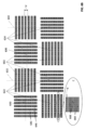
図7Aおよび7Bは、好ましくは4つの構造701、702、704、および706を含んでいるターゲット700を示している。特に図7Aの拡大断面図AおよびBに示されているように、構造701および702が両方とも半導体デバイスウェハの第1の層710上に形成され、構造704および706が両方とも半導体デバイスウェハの第2の層720上に形成されることは、本発明の特定の特徴である。同一の製造ツールおよび方法を使用して構造の対701と702および704と706がそれぞれ同時に形成されることは、本発明の実施形態の特定の特徴である。第1および第2の層710および720が隣接してよいが、隣接する必要はないことが理解される。構造701、702、704、および706の各々が、回転対称性によって特徴付けられ、ターゲット700に回転対称性を与えること注意する。
7A and 7B illustrate a
構造701、702、704、および706が、回転対称性によって特徴付けられた任意の構造であってよいことが、さらに理解される。図7Aおよび7Bでは、ターゲット700が4つの構造を含んでいるように示されているが、ターゲット700は、構造の各対が701と704および702と706のパターンに従う限り、4~20個の範囲内の任意の偶数個の構造を含んでよいことが、さらに理解される。
It is further understood that
構造701、702、704、および706は、通常、セグメント化されるが、セグメント化される必要はない。構造701、702、704、および706がセグメント化される実施形態では、図7Bの拡大図に示されているように、構造701、702、704、および706の各々が、複数の各サブライン760、761、762、および764、ならびにサブライン760、761、762、および764の間の各サブスペース766、767、768、および770によって画定されている。サブライン760、761、762、および764は、それぞれ10~200nmの範囲内の各セグメント化ピッチσ、ε、ζ、およびηを有することが好ましい。構造701、702、704、および706は、それらの各セグメント化ピッチσ、ε、ζ、およびηのいずれかによって互いに区別されることが好ましい。
図1の上記の説明において参照された第1および第2の事例が、構造701と704または構造702と706を使用して取得された位置ずれ測定であってよいことは、本発明の実施形態の特定の特徴である。それに応じて、図1の上記の説明において参照された第1および第2の位置ずれインジケーションは、構造701と704または構造702と706を使用して取得された位置ずれ測定の各々から取得された位置ずれインジケーションであってよい。
It is an embodiment of the present invention that the first and second cases referenced in the above description of FIG. are certain characteristics of Accordingly, the first and second misalignment indications referenced in the above description of FIG. 1 are obtained from each of the misalignment measurements taken using
構造の対701と702および704と706の各々がそれぞれ一緒に形成されることが好ましいため、既定のしきい値を超える、構造701と704の間の位置ずれインジケーション、および702と706の間の位置ずれインジケーションにおける差が、位置ずれ計測プロセスにおける改善の必要性を示すことが、理解される。
Since each of the pairs of
ここで図8を参照すると、図8は、図1~2を参照して上で説明された方法と連動して役立つ、半導体デバイスウェハの製造プロセスのパラメータを変更することによる測定された位置ずれの改善方法800を示す、簡略化されたフローチャートである。 Referring now to FIG. 8, FIG. 8 illustrates measured misalignment by changing parameters of a semiconductor device wafer manufacturing process useful in conjunction with the method described above with reference to FIGS. 1-2. 8 is a simplified flowchart illustrating a method 800 for improving.
以下で説明される方法800が、図2で説明されたプロセスのどの段階が改善を必要とするかを決定するために、図1で説明された方法のステップ150の一部として実行されることが、理解される。 The method 800 described below is performed as part of step 150 of the method illustrated in FIG. 1 to determine which stages of the process illustrated in FIG. 2 require improvement. is understood.
最初のステップ804に示されているように、方法800は、第1および第2の位置ずれインジケーションがリソグラフィ後の位置ずれインジケーション252およびマスク開口後の位置ずれインジケーション254であるかどうかを確認する。 As shown in a first step 804, the method 800 determines whether the first and second misalignment indications are a post-lithography misalignment indication 252 and a post-mask opening misalignment indication 254. confirm.
第1および第2の位置ずれインジケーションがリソグラフィ後の位置ずれインジケーション252およびマスク開口後の位置ずれインジケーション254である場合、方法800は次のステップ806に進み、ステップ806で、さらなる半導体デバイスウェハの処理に備えて、マスク開口段階204が変更される。例えば、マスク開口段階のエッチングの深さが変更されてよく、または測定される層の屈折率もしくは誘電率などの材料特性が変更されてよい。 If the first and second misalignment indications are a post-lithography misalignment indication 252 and a post-mask opening misalignment indication 254, the method 800 continues to a next step 806 where additional semiconductor devices In preparation for processing the wafer, the mask opening step 204 is modified. For example, the etch depth of the mask opening step may be changed, or the material properties such as the refractive index or dielectric constant of the layer being measured may be changed.
第1および第2の位置ずれインジケーションがリソグラフィ後の位置ずれインジケーション252およびマスク開口後の位置ずれインジケーション254でない場合、方法800は次のステップ808に進み、ステップ808で、方法800は、第1および第2の位置ずれインジケーションがリソグラフィ後の位置ずれインジケーション252およびエッチング後の位置ずれインジケーション256であるかどうかを確認する。 If the first and second misalignment indications are not a post-lithography misalignment indication 252 and a post-mask opening misalignment indication 254, the method 800 continues to a next step 808, where the method 800 includes: It is determined whether the first and second misalignment indications are post-lithography misalignment indication 252 and post-etch misalignment indication 256.
第1および第2の位置ずれインジケーションがリソグラフィ後の位置ずれインジケーション252およびエッチング後の位置ずれインジケーション256である場合、方法800は次のステップ810に進み、ステップ810で、さらなる半導体デバイスウェハの処理に備えて、エッチング段階206が変更される。例えば、エッチングの時間が変更されてよく、または測定される層の屈折率もしくは誘電率などの材料特性が変更されてよい。 If the first and second misalignment indications are a post-lithography misalignment indication 252 and a post-etch misalignment indication 256, the method 800 continues to a next step 810 where additional semiconductor device wafers are The etching step 206 is modified in preparation for processing. For example, the etching time may be changed, or the material properties of the layer being measured, such as the refractive index or dielectric constant, may be changed.
第1および第2の位置ずれインジケーションがリソグラフィ後の位置ずれインジケーション252およびエッチング後の位置ずれインジケーション256でない場合、方法800は次のステップ812に進み、ステップ812で、方法800は、第1および第2の位置ずれインジケーションがマスク開口後の位置ずれインジケーション254およびエッチング後の位置ずれインジケーション256であるかどうかを確認する。 If the first and second misalignment indications are not a post-lithography misalignment indication 252 and a post-etch misalignment indication 256, the method 800 continues to the next step 812, where the method 800 It is confirmed whether the first and second positional deviation indications are the positional deviation indication 254 after mask opening and the positional deviation indication 256 after etching.
第1および第2の位置ずれインジケーションがマスク開口後の位置ずれインジケーション254およびエッチング後の位置ずれインジケーション256である場合、方法800は次のステップ814に進み、ステップ814で、さらなる半導体デバイスウェハの処理に備えて、エッチング段階206が変更される。例えば、エッチングの時間が変更されてよく、または測定される層の屈折率もしくは誘電率などの材料特性が変更されてよい。 If the first and second misalignment indications are a post-mask opening misalignment indication 254 and a post-etch misalignment indication 256, the method 800 continues to a next step 814 where additional semiconductor devices In preparation for processing the wafer, the etching step 206 is modified. For example, the etching time may be changed, or the material properties of the layer being measured, such as the refractive index or dielectric constant, may be changed.
第1および第2の位置ずれインジケーションがマスク開口後の位置ずれインジケーション254およびエッチング後の位置ずれインジケーション256でない場合、方法800は次のステップ816に進み、ステップ816で、方法800は、第1および第2の位置ずれインジケーションがリソグラフィ後の位置ずれインジケーション252および研磨後の位置ずれインジケーション258であるかどうかを確認する。 If the first and second misalignment indications are not the post-mask opening misalignment indication 254 and the post-etch misalignment indication 256, the method 800 continues to the next step 816, where the method 800 includes: It is determined whether the first and second misalignment indications are post-lithography misalignment indication 252 and post-polishing misalignment indication 258.
第1および第2の位置ずれインジケーションがリソグラフィ後の位置ずれインジケーション252および研磨後の位置ずれインジケーション258である場合、方法800は次のステップ818に進み、ステップ818で、さらなる半導体デバイスウェハの処理に備えて、エッチング段階206および研磨段階208のうちの少なくとも1つが変更される。例えば、エッチングの時間、研磨の時間、研磨の角度、および研磨段階で使用される材料のいずれかが調整されてよく、または測定される層の屈折率もしくは誘電率などの材料特性が変更されてよい。 If the first and second misalignment indications are a post-lithography misalignment indication 252 and a post-polishing misalignment indication 258, the method 800 continues to a next step 818 where additional semiconductor device wafers are At least one of the etching step 206 and the polishing step 208 is modified in preparation for processing. For example, the etching time, polishing time, polishing angle, and any of the materials used in the polishing step may be adjusted, or material properties such as the refractive index or dielectric constant of the layer being measured are changed. good.
第1および第2の位置ずれインジケーションがリソグラフィ後の位置ずれインジケーション252および研磨後の位置ずれインジケーション258でない場合、方法800は次のステップ820に進み、ステップ820で、方法800は、第1および第2の位置ずれインジケーションがマスク開口後の位置ずれインジケーション254および研磨後の位置ずれインジケーション258であるかどうかを確認する。 If the first and second misalignment indications are not a post-lithography misalignment indication 252 and a post-polishing misalignment indication 258, the method 800 continues to a next step 820, where the method 800 It is confirmed whether the first and second positional deviation indications are the positional deviation indication 254 after mask opening and the positional deviation indication 258 after polishing.
第1および第2の位置ずれインジケーションがマスク開口後の位置ずれインジケーション254および研磨後の位置ずれインジケーション258である場合、方法800は次のステップ822に進み、ステップ822で、さらなる半導体デバイスウェハの処理に備えて、研磨段階208が変更される。例えば、研磨の時間、研磨の角度、および研磨段階で使用される材料のいずれかが調整されてよく、または測定される層の屈折率もしくは誘電率などの材料特性が変更されてよい。 If the first and second misalignment indications are a post-mask opening misalignment indication 254 and a post-polishing misalignment indication 258, the method 800 continues to a next step 822 where additional semiconductor devices In preparation for processing the wafer, the polishing stage 208 is modified. For example, the time of polishing, the angle of polishing, and any of the materials used in the polishing step may be adjusted, or material properties such as the refractive index or dielectric constant of the layer being measured may be changed.
第1および第2の位置ずれインジケーションがマスク開口後の位置ずれインジケーション254および研磨後の位置ずれインジケーション258でない場合、方法800は次のステップ824に進み、ステップ824で、方法800は、第1および第2の位置ずれインジケーションがエッチング後の位置ずれインジケーション256および研磨後の位置ずれインジケーション258であるかどうかを確認する。 If the first and second misalignment indications are not the post-mask opening misalignment indication 254 and the post-polishing misalignment indication 258, the method 800 continues to the next step 824, where the method 800 includes: It is checked whether the first and second misalignment indications are the post-etching misalignment indication 256 and the post-polishing misalignment indication 258.
第1および第2の位置ずれインジケーションがエッチング後の位置ずれインジケーション256および研磨後の位置ずれインジケーション258である場合、方法800は次のステップ826に進み、ステップ826で、さらなる半導体デバイスウェハの処理に備えて、研磨段階208が変更される。例えば、研磨の時間、研磨の角度、および研磨段階で使用される材料のいずれかが調整されてよく、または測定される層の屈折率もしくは誘電率などの材料特性が変更されてよい。 If the first and second misalignment indications are a post-etch misalignment indication 256 and a post-polish misalignment indication 258, the method 800 continues to a next step 826 where additional semiconductor device wafers are The polishing step 208 is modified in preparation for processing. For example, the time of polishing, the angle of polishing, and any of the materials used in the polishing step may be adjusted, or material properties such as the refractive index or dielectric constant of the layer being measured may be changed.
ここで図9Aおよび9Bを参照すると、これらの図は、共に、図1~7を参照して上で説明された方法と連動して役立つ、半導体デバイスウェハの層間の位置ずれの測定に関連する計測パラメータを変更することによる測定された位置ずれの改善方法900を示す、簡略化されたフローチャートである。 Reference is now made to FIGS. 9A and 9B, both of which relate to measuring interlayer misalignment of semiconductor device wafers useful in conjunction with the methods described above with reference to FIGS. 1-7. 9 is a simplified flowchart illustrating a method 900 of improving measured misalignment by changing measurement parameters.
以下で説明される方法900が、方法800の代替手段として、どの計測パラメータが改善を必要とするかを決定するために、図1で説明された方法のステップ150の一部として実行されることが、理解される。本発明の好ましい実施形態では、方法900は、許容できるQメリット値または高い装置起因の誤差などの、他の指標が位置ずれ計測の測定値に問題がある可能性があることを示している場合に、実行される。 As an alternative to method 800, method 900 described below may be performed as part of step 150 of the method described in FIG. 1 to determine which measurement parameters require improvement. is understood. In a preferred embodiment of the invention, the method 900 performs the method 900 if other indicators, such as an acceptable Q-merit value or a high device-induced error, indicate that the misalignment measurement measurement may be problematic. is executed.
第1のステップ902に示されているように、方法900は、非ゼロオフセット(NZO:non-zero offset)校正が実行されるべきかどうかを確認する。NZO校正が実行されるべきである場合、例えば図3~7を参照して上で説明された実施形態では、方法900が次のステップ904に進み、ステップ904でNZO校正が実行される。 As shown in a first step 902, method 900 determines whether a non-zero offset (NZO) calibration is to be performed. If a NZO calibration is to be performed, for example in the embodiments described above with reference to FIGS. 3-7, the method 900 proceeds to the next step 904, where the NZO calibration is performed.
NZO校正が実行されるべきでない場合、方法900が次のステップ908に進み、方法900は、第1および第2の位置ずれインジケーションがリソグラフィ後の位置ずれインジケーション252およびマスク開口後の位置ずれインジケーション254であるかどうかを確認する。 If NZO calibration is not to be performed, the method 900 continues to a next step 908, where the method 900 determines that the first and second misregistration indications are the post-lithography misregistration indication 252 and the post-mask opening misregistration. Check whether the indication is 254 or not.
第1および第2の位置ずれインジケーションがリソグラフィ後の位置ずれインジケーション252およびマスク開口後の位置ずれインジケーション254である場合、方法900は次のステップ910に進み、ステップ910で、リソグラフィ後の位置ずれ測定パラメータおよびマスク開口後の位置ずれ測定パラメータのうちの少なくとも1つが変更される。 If the first and second misregistration indications are a post-lithography misregistration indication 252 and a post-mask opening misregistration indication 254, the method 900 continues to a next step 910 in which the post-lithography misregistration indication 252 and the post-mask opening misregistration indication 254 At least one of the positional deviation measurement parameter and the positional deviation measurement parameter after mask opening is changed.
例えば、リソグラフィ後の位置ずれインジケーション252とマスク開口後の位置ずれインジケーション254の間の差を減らすように、位置ずれが測定される対象領域、位置ずれ測定に利用される光の波長、位置ずれ測定に利用される光の偏光、開口数、回折マスク、および回折開口が調整されてよい。追加の例として、リソグラフィ後の位置ずれ測定およびマスク開口後の位置ずれ測定のうちの少なくとも1つで、中央から遠い測定結果が識別され、測定された位置ずれから除去されてよい。 For example, the target area where the misregistration is measured, the wavelength of the light used for the misregistration measurement, the position, etc., so as to reduce the difference between the post-lithography misregistration indication 252 and the post-mask opening misregistration indication 254. The polarization of the light used for displacement measurement, the numerical aperture, the diffraction mask, and the diffraction aperture may be adjusted. As an additional example, in at least one of a post-lithography misregistration measurement and a post-mask opening misregistration measurement, off-center measurements may be identified and removed from the measured misregistration.
第1および第2の位置ずれインジケーションがリソグラフィ後の位置ずれインジケーション252およびマスク開口後の位置ずれインジケーション254でない場合、方法900は次のステップ912に進み、ステップ912で、方法900は、第1および第2の位置ずれインジケーションがリソグラフィ後の位置ずれインジケーション252およびエッチング後の位置ずれインジケーション256であるかどうかを確認する。 If the first and second misalignment indications are not a post-lithography misalignment indication 252 and a post-mask opening misalignment indication 254, the method 900 continues to a next step 912, where the method 900 includes: It is determined whether the first and second misalignment indications are post-lithography misalignment indication 252 and post-etch misalignment indication 256.
第1および第2の位置ずれインジケーションがリソグラフィ後の位置ずれインジケーション252およびエッチング後の位置ずれインジケーション256である場合、方法900は次のステップ914に進み、ステップ914で、リソグラフィ後の位置ずれ測定パラメータおよびエッチング後の位置ずれ測定パラメータのうちの少なくとも1つが変更される。 If the first and second misregistration indications are a post-lithography misregistration indication 252 and a post-etch misregistration indication 256, the method 900 continues to a next step 914, where the post-lithography position At least one of the displacement measurement parameter and the post-etching position displacement measurement parameter is changed.
例えば、リソグラフィ後の位置ずれインジケーション252とエッチング後の位置ずれインジケーション256の間の差を減らすように、位置ずれが測定される対象領域、位置ずれ測定に利用される光の波長、位置ずれ測定に利用される光の偏光、開口数、回折マスク、および回折開口が調整されてよい。追加の例として、リソグラフィ後の位置ずれ測定およびエッチング後の位置ずれ測定のうちの少なくとも1つで、中央から遠い測定結果が識別され、測定された位置ずれから除去されてよい。 For example, the area of interest in which the misregistration is measured, the wavelength of the light utilized for the misregistration measurement, the misregistration so as to reduce the difference between the post-lithography misregistration indication 252 and the post-etch misregistration indication 256. The polarization of the light used for measurements, the numerical aperture, the diffraction mask, and the diffraction aperture may be adjusted. As an additional example, in at least one of a post-lithography misregistration measurement and a post-etch misregistration measurement, off-center measurements may be identified and removed from the measured misregistration.
第1および第2の位置ずれインジケーションがリソグラフィ後の位置ずれインジケーション252およびエッチング後の位置ずれインジケーション256でない場合、方法900は次のステップ916に進み、ステップ916で、方法900は、第1および第2の位置ずれインジケーションがマスク開口後の位置ずれインジケーション254およびエッチング後の位置ずれインジケーション256であるかどうかを確認する。 If the first and second misalignment indications are not a post-lithography misalignment indication 252 and a post-etch misalignment indication 256, the method 900 continues to a next step 916, where the method 900 It is confirmed whether the first and second positional deviation indications are the positional deviation indication 254 after mask opening and the positional deviation indication 256 after etching.
第1および第2の位置ずれインジケーションがマスク開口後の位置ずれインジケーション254およびエッチング後の位置ずれインジケーション256である場合、方法900は次のステップ918に進み、ステップ918で、マスク開口後の位置ずれ測定パラメータおよびエッチング後の位置ずれ測定パラメータのうちの少なくとも1つが変更される。 If the first and second misalignment indications are a post-mask opening misalignment indication 254 and a post-etch misalignment indication 256, the method 900 continues to a next step 918, in which after the mask opening At least one of the positional deviation measurement parameter and the post-etching positional deviation measurement parameter is changed.
例えば、マスク開口後の位置ずれインジケーション254とエッチング後の位置ずれインジケーション256の間の差を減らすように、位置ずれが測定される対象領域、位置ずれ測定に利用される光の波長、位置ずれ測定に利用される光の偏光、開口数、回折マスク、および回折開口が調整されてよい。追加の例として、マスク開口後の位置ずれ測定およびエッチング後の位置ずれ測定のうちの少なくとも1つで、中央から遠い測定結果が識別され、測定された位置ずれから除去されてよい。 For example, the target area where the misregistration is measured, the wavelength of the light used for the misregistration measurement, the position, etc., so as to reduce the difference between the misregistration indication 254 after mask opening and the misregistration indication 256 after etching. The polarization of the light used for displacement measurement, the numerical aperture, the diffraction mask, and the diffraction aperture may be adjusted. As an additional example, in at least one of a post-mask opening misregistration measurement and a post-etch misregistration measurement, off-center measurements may be identified and removed from the measured misregistration.
第1および第2の位置ずれインジケーションがマスク開口後の位置ずれインジケーション254およびエッチング後の位置ずれインジケーション256でない場合、方法900は次のステップ920に進み、ステップ920で、方法900は、第1および第2の位置ずれインジケーションがリソグラフィ後の位置ずれインジケーション252および研磨後の位置ずれインジケーション258であるかどうかを確認する。 If the first and second misalignment indications are not the post-mask opening misalignment indication 254 and the post-etch misalignment indication 256, the method 900 continues to a next step 920, where the method 900 includes: It is determined whether the first and second misalignment indications are post-lithography misalignment indication 252 and post-polishing misalignment indication 258.
第1および第2の位置ずれインジケーションがリソグラフィ後の位置ずれインジケーション252および研磨後の位置ずれインジケーション258である場合、方法900は次のステップ922に進み、ステップ922で、リソグラフィ後の位置ずれ測定パラメータおよび研磨後の位置ずれ測定パラメータのうちの少なくとも1つが変更される。 If the first and second misregistration indications are a post-lithography misregistration indication 252 and a post-polish misregistration indication 258, the method 900 continues to a next step 922, where the post-lithography misregistration At least one of the displacement measurement parameter and the post-polishing position displacement measurement parameter is changed.
例えば、リソグラフィ後の位置ずれインジケーション252と研磨後の位置ずれインジケーション258の間の差を減らすように、位置ずれが測定される対象領域、位置ずれ測定に利用される光の波長、位置ずれ測定に利用される光の偏光、開口数、回折マスク、および回折開口が調整されてよい。追加の例として、リソグラフィ後の位置ずれ測定および研磨後の位置ずれ測定のうちの少なくとも1つで、中央から遠い測定結果が識別され、測定された位置ずれから除去されてよい。 For example, the region of interest in which the misregistration is measured, the wavelength of the light utilized for the misregistration measurement, the misregistration so as to reduce the difference between the post-lithography misregistration indication 252 and the post-polishing misregistration indication 258. The polarization of the light used for measurements, the numerical aperture, the diffraction mask, and the diffraction aperture may be adjusted. As an additional example, in at least one of a post-lithography misregistration measurement and a post-polishing misregistration measurement, off-center measurements may be identified and removed from the measured misregistration.
第1および第2の位置ずれインジケーションがリソグラフィ後の位置ずれインジケーション252および研磨後の位置ずれインジケーション258でない場合、方法900は次のステップ924に進み、ステップ924で、方法900は、第1および第2の位置ずれインジケーションがマスク開口後の位置ずれインジケーション254および研磨後の位置ずれインジケーション258であるかどうかを確認する。 If the first and second misalignment indications are not the post-lithography misalignment indication 252 and the post-polishing misalignment indication 258, the method 900 continues to the next step 924, where the method 900 It is confirmed whether the first and second positional deviation indications are the positional deviation indication 254 after mask opening and the positional deviation indication 258 after polishing.
第1および第2の位置ずれインジケーションがマスク開口後の位置ずれインジケーション254および研磨後の位置ずれインジケーション258である場合、方法900は次のステップ926に進み、ステップ926で、マスク開口後の位置ずれ測定パラメータおよび研磨後の位置ずれ測定パラメータのうちの少なくとも1つが変更される。 If the first and second misalignment indications are a post-mask opening misalignment indication 254 and a post-polishing misalignment indication 258, the method 900 continues to a next step 926, in which the post-mask opening misalignment indication 254 and the post-polishing misalignment indication 258 At least one of the positional deviation measurement parameter and the post-polishing positional deviation measurement parameter is changed.
例えば、マスク開口後の位置ずれインジケーション254と研磨後の位置ずれインジケーション258の間の差を減らすように、位置ずれが測定される対象領域、位置ずれ測定に利用される光の波長、位置ずれ測定に利用される光の偏光、開口数、回折マスク、および回折開口が調整されてよい。追加の例として、マスク開口後の位置ずれ測定および研磨後の位置ずれ測定のうちの少なくとも1つで、中央から遠い測定結果が識別され、測定された位置ずれから除去されてよい。 For example, the target area where the misregistration is measured, the wavelength of the light used for the misregistration measurement, the position, etc., so as to reduce the difference between the misregistration indication 254 after opening the mask and the misregistration indication 258 after polishing. The polarization of the light used for displacement measurement, the numerical aperture, the diffraction mask, and the diffraction aperture may be adjusted. As an additional example, in at least one of a post-mask opening misregistration measurement and a post-polishing misregistration measurement, off-center measurements may be identified and removed from the measured misregistration.
第1および第2の位置ずれインジケーションがマスク開口後の位置ずれインジケーション254および研磨後の位置ずれインジケーション258でない場合、方法900は次のステップ928に進み、ステップ928で、方法900は、第1および第2の位置ずれインジケーションがエッチング後の位置ずれインジケーション256および研磨後の位置ずれインジケーション258であるかどうかを確認する。 If the first and second misalignment indications are not the post-mask opening misalignment indication 254 and the post-polishing misalignment indication 258, the method 900 continues to the next step 928, where the method 900 includes: It is checked whether the first and second misalignment indications are the post-etching misalignment indication 256 and the post-polishing misalignment indication 258.
第1および第2の位置ずれインジケーションがエッチング後の位置ずれインジケーション256および研磨後の位置ずれインジケーション258である場合、方法900は次のステップ930に進み、ステップ930で、エッチング後の位置ずれ測定パラメータおよび研磨後の位置ずれ測定パラメータのうちの少なくとも1つが変更される。 If the first and second misalignment indications are a post-etch misalignment indication 256 and a post-polish misalignment indication 258, the method 900 continues to a next step 930, where the post-etch position At least one of the displacement measurement parameter and the post-polishing position displacement measurement parameter is changed.
例えば、エッチング後の位置ずれインジケーション256と研磨後の位置ずれインジケーション258の間の差を減らすように、位置ずれが測定される対象領域、位置ずれ測定に利用される光の波長、位置ずれ測定に利用される光の偏光、開口数、回折マスク、および回折開口が調整されてよい。追加の例として、エッチング後の位置ずれ測定および研磨後の位置ずれ測定のうちの少なくとも1つで、中央から遠い測定結果が識別され、測定された位置ずれから除去されてよい。 For example, the target area where misregistration is measured, the wavelength of the light utilized for misregistration measurement, the misregistration so as to reduce the difference between post-etch misregistration indication 256 and post-polish misregistration indication 258. The polarization of the light used for measurements, the numerical aperture, the diffraction mask, and the diffraction aperture may be adjusted. As an additional example, in at least one of a post-etch misregistration measurement and a post-polish misregistration measurement, off-center measurements may be identified and removed from the measured misregistration.
本発明が、上で具体的に示され、説明された内容に限定されないことが、当業者によって理解されるであろう。本発明の範囲は、上で説明されたさまざまな特徴およびそれらの変更の組み合わせおよび部分的組み合わせの両方を含み、それらすべてが先行技術に含まれていない。
It will be understood by those skilled in the art that the invention is not limited to what has been particularly shown and described above. The scope of the invention includes both combinations and subcombinations of the various features described above and variations thereof, not all of which are included in the prior art.
Claims (13)
第1の処理段階後に第1の事例で半導体デバイスウェハの層間の位置ずれを測定して、第1の位置ずれインジケーションを提供することと、
前記第1の処理段階に続く第2の段階後に第2の事例で半導体デバイスウェハの層間の位置ずれを測定して、第2の位置ずれインジケーションを提供することと、
前記第1の位置ずれインジケーションと前記第2の位置ずれインジケーションの間の差に応答して、位置ずれ測定差出力を提供することと、
以前のウェハに関する前記第1の事例と前記第2の事例での位置ずれの差の平均である基準差出力を提供することと、
前記位置ずれ測定差出力と前記基準差出力の間の前記差を改善することとを含むことを特徴とする方法。 1. A method for measuring misalignment in the manufacture of semiconductor device wafers, the method comprising:
measuring interlayer misalignment of the semiconductor device wafer in a first instance after the first processing step to provide a first misalignment indication;
measuring interlayer misalignment of the semiconductor device wafer in a second instance after a second step following the first processing step to provide a second misalignment indication;
providing a misalignment measurement difference output in response to a difference between the first misalignment indication and the second misalignment indication;
providing a reference difference output that is an average of the difference in misalignment between the first case and the second case for previous wafers;
improving the difference between the misalignment measurement difference output and the reference difference output.
位置ずれ計測を変更することと、
半導体デバイスウェハの前記製造における少なくとも1つの処理ステップを変更すること、
のうちの少なくとも1つを含むことを特徴とする方法。 2. The method of claim 1, wherein the improving comprises:
changing the positional deviation measurement;
modifying at least one processing step in said manufacturing of semiconductor device wafers;
A method comprising at least one of:
Priority Applications (1)
| Application Number | Priority Date | Filing Date | Title |
|---|---|---|---|
| JP2023119592A JP2023126665A (en) | 2019-03-28 | 2023-07-24 | target |
Applications Claiming Priority (3)
| Application Number | Priority Date | Filing Date | Title |
|---|---|---|---|
| US201962825262P | 2019-03-28 | 2019-03-28 | |
| US62/825,262 | 2019-03-28 | ||
| PCT/US2019/030776 WO2020197571A1 (en) | 2019-03-28 | 2019-05-06 | Method for measuring and correcting misregistration between layers in a semiconductor device, and misregistration targets useful therein |
Related Child Applications (1)
| Application Number | Title | Priority Date | Filing Date |
|---|---|---|---|
| JP2023119592A Division JP2023126665A (en) | 2019-03-28 | 2023-07-24 | target |
Publications (2)
| Publication Number | Publication Date |
|---|---|
| JP2022529749A JP2022529749A (en) | 2022-06-23 |
| JP7345572B2 true JP7345572B2 (en) | 2023-09-15 |
Family
ID=72609096
Family Applications (2)
| Application Number | Title | Priority Date | Filing Date |
|---|---|---|---|
| JP2021576144A Active JP7345572B2 (en) | 2019-03-28 | 2019-05-06 | Methods for measuring and correcting misalignment between layers in semiconductor devices, and misalignment targets useful therein |
| JP2023119592A Pending JP2023126665A (en) | 2019-03-28 | 2023-07-24 | target |
Family Applications After (1)
| Application Number | Title | Priority Date | Filing Date |
|---|---|---|---|
| JP2023119592A Pending JP2023126665A (en) | 2019-03-28 | 2023-07-24 | target |
Country Status (5)
| Country | Link |
|---|---|
| US (2) | US11302544B2 (en) |
| EP (1) | EP3948937A4 (en) |
| JP (2) | JP7345572B2 (en) |
| CN (1) | CN113924638A (en) |
| WO (1) | WO2020197571A1 (en) |
Families Citing this family (3)
| Publication number | Priority date | Publication date | Assignee | Title |
|---|---|---|---|---|
| US11454894B2 (en) | 2020-09-14 | 2022-09-27 | Kla Corporation | Systems and methods for scatterometric single-wavelength measurement of misregistration and amelioration thereof |
| US20220392809A1 (en) * | 2021-06-03 | 2022-12-08 | Kla Corporation | Adaptive modeling misregistration measurement system and method |
| CN115881563A (en) * | 2021-09-28 | 2023-03-31 | 上海华力集成电路制造有限公司 | Method for improving overlay measurement accuracy of self-aligned multi-imaging technology |
Citations (4)
| Publication number | Priority date | Publication date | Assignee | Title |
|---|---|---|---|---|
| JP2003163163A (en) | 2002-12-12 | 2003-06-06 | Nikon Corp | Position alignment method, exposure method and device manufacturing method |
| JP2005181636A (en) | 2003-12-18 | 2005-07-07 | Toshiba Corp | Method and system for pattern verification, method for manufacturing mask, and method for manufacturing semiconductor device |
| JP2009014830A (en) | 2007-07-02 | 2009-01-22 | Dainippon Screen Mfg Co Ltd | Pattern data generating device, exposure system, pattern data generation method and program |
| JP2018522283A (en) | 2015-07-13 | 2018-08-09 | エーエスエムエル ネザーランズ ビー.ブイ. | Lithographic apparatus and device manufacturing method |
Family Cites Families (14)
| Publication number | Priority date | Publication date | Assignee | Title |
|---|---|---|---|---|
| US5699282A (en) * | 1994-04-28 | 1997-12-16 | The United States Of America As Represented By The Secretary Of Commerce | Methods and test structures for measuring overlay in multilayer devices |
| JP3927353B2 (en) | 2000-06-15 | 2007-06-06 | 株式会社日立製作所 | Image alignment method, comparison inspection method, and comparison inspection apparatus in comparison inspection |
| US7068833B1 (en) * | 2000-08-30 | 2006-06-27 | Kla-Tencor Corporation | Overlay marks, methods of overlay mark design and methods of overlay measurements |
| US20030002043A1 (en) * | 2001-04-10 | 2003-01-02 | Kla-Tencor Corporation | Periodic patterns and technique to control misalignment |
| US6774998B1 (en) * | 2001-12-27 | 2004-08-10 | Advanced Micro Devices, Inc. | Method and apparatus for identifying misregistration in a complimentary phase shift mask process |
| US9927718B2 (en) | 2010-08-03 | 2018-03-27 | Kla-Tencor Corporation | Multi-layer overlay metrology target and complimentary overlay metrology measurement systems |
| CN106684041B (en) * | 2015-11-10 | 2020-12-08 | 联华电子股份有限公司 | Semiconductor element and manufacturing method thereof |
| US9754895B1 (en) | 2016-03-07 | 2017-09-05 | Micron Technology, Inc. | Methods of forming semiconductor devices including determining misregistration between semiconductor levels and related apparatuses |
| KR102426823B1 (en) * | 2016-09-30 | 2022-07-28 | 가부시키가이샤 니콘 | Measuring system, substrate processing system, and device manufacturing method |
| US9786569B1 (en) * | 2016-10-26 | 2017-10-10 | Taiwan Semiconductor Manufacturing Co., Ltd. | Overlay measurement and compensation in semiconductor fabrication |
| KR102259091B1 (en) | 2016-11-10 | 2021-06-01 | 에이에스엠엘 네델란즈 비.브이. | Design and Calibration Using Stack Differences |
| KR102434050B1 (en) * | 2016-12-02 | 2022-08-19 | 에이에스엠엘 네델란즈 비.브이. | A method to change an etch parameter |
| EP3330797A1 (en) * | 2016-12-02 | 2018-06-06 | ASML Netherlands B.V. | A method to change an etch parameter |
| US10409171B2 (en) | 2017-01-25 | 2019-09-10 | Kla-Tencor Corporation | Overlay control with non-zero offset prediction |
-
2019
- 2019-05-06 US US16/467,968 patent/US11302544B2/en active Active
- 2019-05-06 CN CN201980096802.8A patent/CN113924638A/en active Pending
- 2019-05-06 WO PCT/US2019/030776 patent/WO2020197571A1/en unknown
- 2019-05-06 EP EP19921663.1A patent/EP3948937A4/en active Pending
- 2019-05-06 JP JP2021576144A patent/JP7345572B2/en active Active
-
2022
- 2022-03-07 US US17/688,856 patent/US20220199437A1/en active Pending
-
2023
- 2023-07-24 JP JP2023119592A patent/JP2023126665A/en active Pending
Patent Citations (4)
| Publication number | Priority date | Publication date | Assignee | Title |
|---|---|---|---|---|
| JP2003163163A (en) | 2002-12-12 | 2003-06-06 | Nikon Corp | Position alignment method, exposure method and device manufacturing method |
| JP2005181636A (en) | 2003-12-18 | 2005-07-07 | Toshiba Corp | Method and system for pattern verification, method for manufacturing mask, and method for manufacturing semiconductor device |
| JP2009014830A (en) | 2007-07-02 | 2009-01-22 | Dainippon Screen Mfg Co Ltd | Pattern data generating device, exposure system, pattern data generation method and program |
| JP2018522283A (en) | 2015-07-13 | 2018-08-09 | エーエスエムエル ネザーランズ ビー.ブイ. | Lithographic apparatus and device manufacturing method |
Also Published As
| Publication number | Publication date |
|---|---|
| WO2020197571A1 (en) | 2020-10-01 |
| CN113924638A (en) | 2022-01-11 |
| JP2023126665A (en) | 2023-09-07 |
| EP3948937A4 (en) | 2023-02-15 |
| US11302544B2 (en) | 2022-04-12 |
| TW202105550A (en) | 2021-02-01 |
| US20220199437A1 (en) | 2022-06-23 |
| US20200312687A1 (en) | 2020-10-01 |
| JP2022529749A (en) | 2022-06-23 |
| EP3948937A1 (en) | 2022-02-09 |
Similar Documents
| Publication | Publication Date | Title |
|---|---|---|
| JP2023126665A (en) | target | |
| US9316925B2 (en) | Methods for monitoring source symmetry of photolithography systems | |
| KR101853990B1 (en) | Method and system for providing process tool correctables | |
| US9927719B2 (en) | Overlay sampling methodology | |
| KR102467186B1 (en) | Test structures and metrology technique utilizing the test structures for measuring in patterned structures | |
| WO2003075342A2 (en) | Methodology for repeatable post etch cd in a production tool | |
| JP4511582B2 (en) | Mask pattern correction method, photomask, and semiconductor device manufacturing method | |
| US20230122820A1 (en) | Semiconductor marks and forming methods thereof | |
| TWI804708B (en) | Misregistration metrology system, method for manufacturing semiconductor device wafers, and target for use in measurement of misregistration | |
| US6808942B1 (en) | Method for controlling a critical dimension (CD) in an etch process | |
| TW202043750A (en) | Parameter-stable misregistration measurement amelioration in semiconductor devices | |
| US8234602B2 (en) | Semiconductor-device manufacturing method | |
| TWI836001B (en) | Method for measuring and correcting misregistration between layers in a semiconductor device, and misregistration targets useful therein | |
| CN116203808A (en) | Overlay error measurement method and overlay mark | |
| CN115524943A (en) | Method and system for establishing optical critical dimension database | |
| US20080044739A1 (en) | Correction Of Resist Critical Dimension Variations In Lithography Processes | |
| CN110767572B (en) | Method for monitoring step height of junction region of active region and isolation structure | |
| TW201539145A (en) | Overlay metrology method | |
| JP2012164811A (en) | Method of manufacturing semiconductor device, method of determining shipping of exposure mask and method of manufacturing exposure mask | |
| CN114077153A (en) | Chip manufacturing method | |
| TW494512B (en) | In-situ post-develop inspection performing in polysilicon etch platform system | |
| CN114660892A (en) | Method of managing critical dimension errors and method of manufacturing a photomask | |
| KR20050069342A (en) | Semiconductor wafer having patterns for monitoring thickness of layer and method for monitoring thickness of layer using such patterns | |
| JPWO2020167331A5 (en) | ||
| JP2007066941A (en) | Method for forming groove for wiring of semiconductor device |
Legal Events
| Date | Code | Title | Description |
|---|---|---|---|
| A521 | Request for written amendment filed |
Free format text: JAPANESE INTERMEDIATE CODE: A523 Effective date: 20220427 |
|
| A621 | Written request for application examination |
Free format text: JAPANESE INTERMEDIATE CODE: A621 Effective date: 20220427 |
|
| A131 | Notification of reasons for refusal |
Free format text: JAPANESE INTERMEDIATE CODE: A131 Effective date: 20230425 |
|
| A521 | Request for written amendment filed |
Free format text: JAPANESE INTERMEDIATE CODE: A523 Effective date: 20230724 |
|
| TRDD | Decision of grant or rejection written | ||
| A01 | Written decision to grant a patent or to grant a registration (utility model) |
Free format text: JAPANESE INTERMEDIATE CODE: A01 Effective date: 20230815 |
|
| A61 | First payment of annual fees (during grant procedure) |
Free format text: JAPANESE INTERMEDIATE CODE: A61 Effective date: 20230905 |
|
| R150 | Certificate of patent or registration of utility model |
Ref document number: 7345572 Country of ref document: JP Free format text: JAPANESE INTERMEDIATE CODE: R150 |