JP7337331B2 - 共振子及び共振装置 - Google Patents
共振子及び共振装置 Download PDFInfo
- Publication number
- JP7337331B2 JP7337331B2 JP2021527381A JP2021527381A JP7337331B2 JP 7337331 B2 JP7337331 B2 JP 7337331B2 JP 2021527381 A JP2021527381 A JP 2021527381A JP 2021527381 A JP2021527381 A JP 2021527381A JP 7337331 B2 JP7337331 B2 JP 7337331B2
- Authority
- JP
- Japan
- Prior art keywords
- resonator
- vibrating
- axis direction
- vibrating portion
- width
- Prior art date
- Legal status (The legal status is an assumption and is not a legal conclusion. Google has not performed a legal analysis and makes no representation as to the accuracy of the status listed.)
- Active
Links
Images


Classifications
-
- H—ELECTRICITY
- H03—ELECTRONIC CIRCUITRY
- H03H—IMPEDANCE NETWORKS, e.g. RESONANT CIRCUITS; RESONATORS
- H03H9/00—Networks comprising electromechanical or electro-acoustic elements; Electromechanical resonators
- H03H9/24—Constructional features of resonators of material which is not piezoelectric, electrostrictive, or magnetostrictive
- H03H9/2405—Constructional features of resonators of material which is not piezoelectric, electrostrictive, or magnetostrictive of microelectro-mechanical resonators
-
- H—ELECTRICITY
- H03—ELECTRONIC CIRCUITRY
- H03H—IMPEDANCE NETWORKS, e.g. RESONANT CIRCUITS; RESONATORS
- H03H9/00—Networks comprising electromechanical or electro-acoustic elements; Electromechanical resonators
- H03H9/02—Details
- H03H9/05—Holders or supports
- H03H9/0595—Holders or supports the holder support and resonator being formed in one body
-
- H—ELECTRICITY
- H03—ELECTRONIC CIRCUITRY
- H03H—IMPEDANCE NETWORKS, e.g. RESONANT CIRCUITS; RESONATORS
- H03H9/00—Networks comprising electromechanical or electro-acoustic elements; Electromechanical resonators
- H03H9/02—Details
- H03H9/05—Holders or supports
- H03H9/0538—Constructional combinations of supports or holders with electromechanical or other electronic elements
-
- H—ELECTRICITY
- H03—ELECTRONIC CIRCUITRY
- H03H—IMPEDANCE NETWORKS, e.g. RESONANT CIRCUITS; RESONATORS
- H03H9/00—Networks comprising electromechanical or electro-acoustic elements; Electromechanical resonators
- H03H9/02—Details
- H03H9/05—Holders or supports
- H03H9/10—Mounting in enclosures
- H03H9/1057—Mounting in enclosures for microelectro-mechanical devices
-
- H—ELECTRICITY
- H03—ELECTRONIC CIRCUITRY
- H03H—IMPEDANCE NETWORKS, e.g. RESONANT CIRCUITS; RESONATORS
- H03H9/00—Networks comprising electromechanical or electro-acoustic elements; Electromechanical resonators
- H03H9/15—Constructional features of resonators consisting of piezoelectric or electrostrictive material
- H03H9/17—Constructional features of resonators consisting of piezoelectric or electrostrictive material having a single resonator
- H03H9/171—Constructional features of resonators consisting of piezoelectric or electrostrictive material having a single resonator implemented with thin-film techniques, i.e. of the film bulk acoustic resonator [FBAR] type
-
- H—ELECTRICITY
- H03—ELECTRONIC CIRCUITRY
- H03H—IMPEDANCE NETWORKS, e.g. RESONANT CIRCUITS; RESONATORS
- H03H9/00—Networks comprising electromechanical or electro-acoustic elements; Electromechanical resonators
- H03H9/02—Details
- H03H9/02244—Details of microelectro-mechanical resonators
- H03H2009/02488—Vibration modes
- H03H2009/02496—Horizontal, i.e. parallel to the substrate plane
- H03H2009/02503—Breath-like, e.g. Lam? mode, wine-glass mode
Landscapes
- Physics & Mathematics (AREA)
- Acoustics & Sound (AREA)
- Piezo-Electric Or Mechanical Vibrators, Or Delay Or Filter Circuits (AREA)
Description
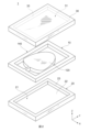
まず、図1及び図2を参照しつつ、本発明の第1実施形態に係る共振装置の概略構成について説明する。図1は、第1実施形態における共振装置1の外観を概略的に示す斜視図である。図2は、図1に示した共振装置1の構造を概略的に示す分解斜視図である。
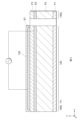
図10は、図3に示した共振子10の変形例を示す平面図である。なお、図10に示す共振子10’の積層構造は、図4及び図5に示した共振子10の断面の構成と同様であるため、図示及びその構成についての説明を省略する。
次に、図11から図15を参照しつつ、本発明の第2実施形態に係る共振装置及び共振子について説明する。なお、第1実施形態と同一又は類似の構成について同一又は類似の符号を付している。以下、第1実施形態と異なる点について説明する。また、同様の構成による同様の作用効果については、逐次言及しない。
次に、図16及び図17を参照しつつ、本発明の第3実施形態に係る共振装置及び共振子について説明する。なお、第1実施形態及び第2実施形態と同一又は類似の構成について同一又は類似の符号を付している。以下、第1実施形態及び第2実施形態と異なる点について説明する。また、同様の構成による同様の作用効果については、逐次言及しない。
Claims (12)
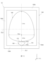
- 第1主面が第1方向の幅と第2方向の長さとを有する基板を含み、
輪郭振動を主振動として振動する振動部と、
前記振動部の少なくとも一部を囲むように形成される保持部と、
前記第2方向に沿って延在し、前記保持部と前記振動部における前記第2方向の一端部とを接続する支持部と、を備え、
前記振動部は、前記第1主面を平面視したときに、前記第1方向の幅が、前記第2方向の一端部から他端部に向けて前記振動部の全域に亘って変化するように構成され、かつ、前記第1方向の幅が、最大となる前記第2方向の位置から前記一端部に向けて、及び前記位置から前記第2方向の他端部に向けて、小さくなり、
前記位置は、前記振動部における前記第2方向の中心からずれている、
共振子。 - 前記振動部は、前記第1主面を平面視したときに、前記第1方向の幅が、最大となる前記第2方向の位置から前記一端部に向けて、及び前記位置から前記第2方向の他端部に向けて、前記振動部の全域に亘って漸次的に小さくなる、
請求項1に記載の共振子。 - 前記位置は、前記振動部における前記第2方向の中心から前記一端部側にずれている、
請求項1または2に記載の共振子。 - 前記第2方向の長さは、前記第1方向の幅より大きい、
請求項1から3のいずれか一項に記載の共振子。 - 前記支持部は、前記一端部における前記第1方向の中央部と接続される、
請求項1から4のいずれか一項に記載の共振子。 - 前記振動部は、第1電極と、前記基板と前記第1電極との間に配置される圧電体層とを含む、
請求項1から5のいずれか一項に記載の共振子。 - 前記振動部は、前記基板と前記圧電体層との間に配置される第2電極をさらに含む、
請求項6に記載の共振子。 - 前記振動部は、前記第1電極を覆うように形成される保護層をさらに含む、
請求項6または7に記載の共振子。 - 前記基板の材料は、シリコンである、
請求項1から8のいずれか一項に記載の共振子。 - 前記基板の材料は、縮退シリコンである、
請求項1から8のいずれか一項に記載の共振子。 - 前記振動部は、前記基板の第2主面に形成される補正層をさらに含む、
請求項1から10のいずれか一項に記載の共振子。 - 請求項1から11のいずれか一項に記載の共振子と、
蓋体と、を備える、
共振装置。
Applications Claiming Priority (3)
| Application Number | Priority Date | Filing Date | Title |
|---|---|---|---|
| JP2019112082 | 2019-06-17 | ||
| JP2019112082 | 2019-06-17 | ||
| PCT/JP2020/013712 WO2020255520A1 (ja) | 2019-06-17 | 2020-03-26 | 共振子及び共振装置 |
Publications (3)
| Publication Number | Publication Date |
|---|---|
| JPWO2020255520A1 JPWO2020255520A1 (ja) | 2020-12-24 |
| JPWO2020255520A5 JPWO2020255520A5 (ja) | 2022-03-04 |
| JP7337331B2 true JP7337331B2 (ja) | 2023-09-04 |
Family
ID=74040458
Family Applications (1)
| Application Number | Title | Priority Date | Filing Date |
|---|---|---|---|
| JP2021527381A Active JP7337331B2 (ja) | 2019-06-17 | 2020-03-26 | 共振子及び共振装置 |
Country Status (4)
| Country | Link |
|---|---|
| US (1) | US12413205B2 (ja) |
| JP (1) | JP7337331B2 (ja) |
| CN (1) | CN113940001B (ja) |
| WO (1) | WO2020255520A1 (ja) |
Families Citing this family (1)
| Publication number | Priority date | Publication date | Assignee | Title |
|---|---|---|---|---|
| US11552613B2 (en) * | 2019-04-19 | 2023-01-10 | Akoustis, Inc. | Resonator shapes for bulk acoustic wave (BAW) devices |
Citations (5)
| Publication number | Priority date | Publication date | Assignee | Title |
|---|---|---|---|---|
| JP2013143640A (ja) | 2012-01-10 | 2013-07-22 | Seiko Instruments Inc | 水晶振動子及び水晶振動子の製造方法 |
| JP2015167222A (ja) | 2014-02-12 | 2015-09-24 | セイコーインスツル株式会社 | 電子部品 |
| JP2017169107A (ja) | 2016-03-17 | 2017-09-21 | 株式会社大真空 | 圧電振動片および当該圧電振動片を用いた圧電振動子 |
| WO2018008198A1 (ja) | 2016-07-05 | 2018-01-11 | 株式会社村田製作所 | 共振子及び共振装置 |
| WO2019008830A1 (ja) | 2017-07-05 | 2019-01-10 | 株式会社村田製作所 | 共振子及び共振装置 |
Family Cites Families (11)
| Publication number | Priority date | Publication date | Assignee | Title |
|---|---|---|---|---|
| JP3139274B2 (ja) | 1993-04-14 | 2001-02-26 | 株式会社村田製作所 | 幅拡がりモードを利用した振動体、共振子及び共振部品 |
| JP3969224B2 (ja) * | 2002-01-08 | 2007-09-05 | 株式会社村田製作所 | 圧電共振子及びそれを用いた圧電フィルタ・デュプレクサ・通信装置 |
| JP4908156B2 (ja) * | 2006-11-10 | 2012-04-04 | 株式会社日立製作所 | 薄膜圧電振動子及び薄膜圧電バルク波共振器及びそれを用いた高周波フィルタ |
| US7834526B2 (en) * | 2007-04-10 | 2010-11-16 | Seiko Epson Corporation | Contour resonator |
| US7586239B1 (en) * | 2007-06-06 | 2009-09-08 | Rf Micro Devices, Inc. | MEMS vibrating structure using a single-crystal piezoelectric thin film layer |
| US8729779B2 (en) * | 2009-04-09 | 2014-05-20 | The Trustees Of The University Of Pennsylvania | Wide bandwidth slanted-finger contour-mode piezoelectric devices |
| TW201238244A (en) * | 2011-02-23 | 2012-09-16 | Nihon Dempa Kogyo Co | GT-cut quartz crystal resonator |
| US8907549B2 (en) * | 2011-09-05 | 2014-12-09 | Nihon Dempa Kogyo Co., Ltd. | Tuning fork configured to generate flexural vibration in reverse phase to the contour vibration of first and second vibrating bodies |
| US9276556B1 (en) * | 2012-09-20 | 2016-03-01 | University Of South Florida | Micromechanical devices based on piezoelectric resonators |
| JP6338367B2 (ja) * | 2013-12-24 | 2018-06-06 | 日本電波工業株式会社 | 水晶振動子 |
| EP3444947B1 (en) * | 2016-05-26 | 2023-03-22 | Murata Manufacturing Co., Ltd. | Resonator and resonance device |
-
2020
- 2020-03-26 CN CN202080042341.9A patent/CN113940001B/zh active Active
- 2020-03-26 WO PCT/JP2020/013712 patent/WO2020255520A1/ja not_active Ceased
- 2020-03-26 JP JP2021527381A patent/JP7337331B2/ja active Active
-
2021
- 2021-12-02 US US17/540,324 patent/US12413205B2/en active Active
Patent Citations (5)
| Publication number | Priority date | Publication date | Assignee | Title |
|---|---|---|---|---|
| JP2013143640A (ja) | 2012-01-10 | 2013-07-22 | Seiko Instruments Inc | 水晶振動子及び水晶振動子の製造方法 |
| JP2015167222A (ja) | 2014-02-12 | 2015-09-24 | セイコーインスツル株式会社 | 電子部品 |
| JP2017169107A (ja) | 2016-03-17 | 2017-09-21 | 株式会社大真空 | 圧電振動片および当該圧電振動片を用いた圧電振動子 |
| WO2018008198A1 (ja) | 2016-07-05 | 2018-01-11 | 株式会社村田製作所 | 共振子及び共振装置 |
| WO2019008830A1 (ja) | 2017-07-05 | 2019-01-10 | 株式会社村田製作所 | 共振子及び共振装置 |
Also Published As
| Publication number | Publication date |
|---|---|
| CN113940001B (zh) | 2025-09-23 |
| JPWO2020255520A1 (ja) | 2020-12-24 |
| US20220094332A1 (en) | 2022-03-24 |
| US12413205B2 (en) | 2025-09-09 |
| CN113940001A (zh) | 2022-01-14 |
| WO2020255520A1 (ja) | 2020-12-24 |
Similar Documents
| Publication | Publication Date | Title |
|---|---|---|
| US10673404B2 (en) | Resonator and resonation device | |
| JP6468350B2 (ja) | 共振子及び共振装置 | |
| US10715103B2 (en) | Resonator and resonance device | |
| US10879448B2 (en) | Resonator and resonator device | |
| JPWO2018008480A1 (ja) | 共振子及び共振装置 | |
| JP6646899B2 (ja) | 共振子及び共振装置 | |
| CN107925394B (zh) | 谐振子和谐振装置 | |
| US12155369B2 (en) | Resonator and resonance device for vibrating in a contour vibration mode | |
| JP7337331B2 (ja) | 共振子及び共振装置 | |
| JP6814419B2 (ja) | 共振子及び共振装置 | |
| JP7400955B2 (ja) | 共振子および共振装置 | |
| WO2019111439A1 (ja) | 共振子、及び共振装置 | |
| US11411546B2 (en) | Resonance device and method for manufacturing resonance device | |
| WO2020153287A1 (ja) | 共振子及び共振装置 | |
| WO2017195416A1 (ja) | 共振子及び共振装置 |
Legal Events
| Date | Code | Title | Description |
|---|---|---|---|
| A521 | Request for written amendment filed |
Free format text: JAPANESE INTERMEDIATE CODE: A523 Effective date: 20211207 |
|
| A621 | Written request for application examination |
Free format text: JAPANESE INTERMEDIATE CODE: A621 Effective date: 20211207 |
|
| A131 | Notification of reasons for refusal |
Free format text: JAPANESE INTERMEDIATE CODE: A131 Effective date: 20220930 |
|
| A521 | Request for written amendment filed |
Free format text: JAPANESE INTERMEDIATE CODE: A523 Effective date: 20221125 |
|
| A131 | Notification of reasons for refusal |
Free format text: JAPANESE INTERMEDIATE CODE: A131 Effective date: 20230320 |
|
| A521 | Request for written amendment filed |
Free format text: JAPANESE INTERMEDIATE CODE: A523 Effective date: 20230426 |
|
| TRDD | Decision of grant or rejection written | ||
| A01 | Written decision to grant a patent or to grant a registration (utility model) |
Free format text: JAPANESE INTERMEDIATE CODE: A01 Effective date: 20230724 |
|
| A61 | First payment of annual fees (during grant procedure) |
Free format text: JAPANESE INTERMEDIATE CODE: A61 Effective date: 20230806 |
|
| R150 | Certificate of patent or registration of utility model |
Ref document number: 7337331 Country of ref document: JP Free format text: JAPANESE INTERMEDIATE CODE: R150 |