JP7327646B2 - Displacement sensor and performance control device - Google Patents
Displacement sensor and performance control device Download PDFInfo
- Publication number
- JP7327646B2 JP7327646B2 JP2022507186A JP2022507186A JP7327646B2 JP 7327646 B2 JP7327646 B2 JP 7327646B2 JP 2022507186 A JP2022507186 A JP 2022507186A JP 2022507186 A JP2022507186 A JP 2022507186A JP 7327646 B2 JP7327646 B2 JP 7327646B2
- Authority
- JP
- Japan
- Prior art keywords
- coil
- wiring pattern
- insulating layer
- detected
- magnetic field
- Prior art date
- Legal status (The legal status is an assumption and is not a legal conclusion. Google has not performed a legal analysis and makes no representation as to the accuracy of the status listed.)
- Active
Links
Images


Classifications
-
- G—PHYSICS
- G01—MEASURING; TESTING
- G01B—MEASURING LENGTH, THICKNESS OR SIMILAR LINEAR DIMENSIONS; MEASURING ANGLES; MEASURING AREAS; MEASURING IRREGULARITIES OF SURFACES OR CONTOURS
- G01B7/00—Measuring arrangements characterised by the use of electric or magnetic techniques
-
- G—PHYSICS
- G10—MUSICAL INSTRUMENTS; ACOUSTICS
- G10H—ELECTROPHONIC MUSICAL INSTRUMENTS; INSTRUMENTS IN WHICH THE TONES ARE GENERATED BY ELECTROMECHANICAL MEANS OR ELECTRONIC GENERATORS, OR IN WHICH THE TONES ARE SYNTHESISED FROM A DATA STORE
- G10H1/00—Details of electrophonic musical instruments
- G10H1/32—Constructional details
- G10H1/34—Switch arrangements, e.g. keyboards or mechanical switches specially adapted for electrophonic musical instruments
Description
本開示は、変位センサーおよび演奏操作装置に関する。 TECHNICAL FIELD The present disclosure relates to displacement sensors and performance operating devices.
例えば鍵盤楽器における鍵等の可動部材の変位を検出するための各種の技術が、従来から提案されている。特許文献1には、固定部材に設置された励磁コイルおよび位置検出コイルと、固定部材に対して移動する可動部材に設置された被励磁コイルとを利用して、可動部材の変位を検出する構成が開示されている。励磁コイルと位置検出コイルと被励磁コイルとの各々は、可動部材が移動する方向に平行な環状に形成される。このような構成において、周期信号の供給により励磁コイルに磁界を発生させることで、被励磁コイルに電磁誘導による磁界が発生する。被励磁コイルの磁界に応じて位置検出コイルに発生する誘導電圧が、可動部材の位置を表す検出信号として生成される。
For example, various techniques have been proposed for detecting displacement of movable members such as keys in keyboard instruments.
しかしながら、特許文献1の技術において、可動部材をメンテナンスする際に、工具等によって、可動部材に設置されたコイルを損傷してしまう可能性があった。このような事情を考慮して、本開示のひとつの態様は、可動部材に設置されるコイルの損傷を低減することを目的とする。
However, in the technique disclosed in
上記目的を達成するために、本開示の一態様に係る変位センサーは、操作に応じた可動部材の変位を検出する変位センサーであって、前記可動部材に設置され、絶縁性樹脂により形成された保護部材で保護された第1コイルを含む被検出部と、電流の供給により磁界を発生する第2コイルを含み、前記被検出部の第1コイルとそれに対向する前記第2コイルとの相対位置に応じた検出信号を生成する信号生成部と、を具備する。 To achieve the above object, a displacement sensor according to one aspect of the present disclosure is a displacement sensor that detects displacement of a movable member according to an operation, is installed on the movable member, and is made of an insulating resin. A relative position between the first coil of the detected part including a first coil protected by a protective member and the second coil that generates a magnetic field when supplied with a current, and the second coil facing it. and a signal generation unit that generates a detection signal according to.
A:第1実施形態
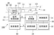
図1は、本開示の第1実施形態に係る変位センサーを適用した鍵盤楽器100の構成を例示するブロック図である。
鍵盤楽器100は、鍵盤10と検出システム15と情報処理装置30と放音装置40とを具備する電子楽器である。鍵盤10は、複数の白鍵と複数の黒鍵とを含む複数の鍵12で構成される。複数の鍵12の各々は、利用者による演奏動作に応じて変位する可動部材である。検出システム15は、鍵12の変位(位置)を検出する。情報処理装置30は、検出システム15による検出の結果に応じた音響信号Vを生成する。音響信号Vは、利用者が操作した鍵12に対応する音高の楽音を表す信号である。放音装置40は、音響信号Vが表す音響を放音する。例えばスピーカまたはヘッドホンが放音装置40として利用される。A: First Embodiment FIG. 1 is a block diagram illustrating the configuration of a
A
図2は、鍵盤10のうち、1個の鍵12に着目して鍵盤楽器100の具体的な構成を例示するブロック図である。鍵盤10の各鍵12は、支点部(バランスピン)13を支点として支持部材14に支持される。支持部材14は、鍵盤楽器100の各要素を支持する構造体である。各鍵12の端部121は、利用者による押鍵および離鍵により鉛直方向に変位する。検出システム15は、複数の鍵12の各々について、鉛直方向における端部121の位置Zに応じたレベルの検出信号Dを生成する。位置Zは、例えば、鍵12に荷重が作用しない解放状態における端部121の位置を基準とした当該端部121の変位量で表現される。
FIG. 2 is a block diagram illustrating a specific configuration of the
検出システム15は、鍵12毎に設けられる変位センサー20と各鍵12に共通の信号処理回路21とを具備する。変位センサー20は、各鍵12の位置を検出する位置センサーであり、被検出部50と信号生成部60とを含む。信号生成部60は、支持部材14に設置される。被検出部50は、鍵12に設置される。具体的には、被検出部50は、鍵12の底面(以下「設置面」という)122に設置される。被検出部50は第1コイル51を含む。信号生成部60は第2コイル61を含む。第1コイル51と第2コイル61とは、鉛直方向に相互に間隔をあけて対向する。信号生成部60と被検出部50との距離(第1コイル51と第2コイル61との距離)は、押鍵および離鍵により鍵12における端部121の位置Zが変化することに応じて変化する。
The
図3は、変位センサー20を構成する被検出部50と信号生成部60とにおける電気的な構成を例示する回路図である。信号生成部60は、入力端子T1と出力端子T2と第2コイル61と容量素子62と容量素子63と抵抗素子64とを含む。第2コイル61と容量素子62と容量素子63と抵抗素子64とによって共振回路が構成される。入力端子T1は抵抗素子64の一端に接続され、抵抗素子64の他端は容量素子62の一端および第2コイル61の一端に接続される。第2コイル61の他端は出力端子T2および容量素子63の一端に接続される。容量素子62の他端および容量素子63の他端は、電圧ゼロの基準である電位Gndに接地される。
FIG. 3 is a circuit diagram illustrating an electrical configuration of the detected
一方、被検出部50は、第1コイル51と容量素子52とを含む。第1コイル51の一端と容量素子52の一端とが相互に接続され、第1コイル51の他端と容量素子52の他端とが相互に接続される。第1コイル51と容量素子52とによって共振回路が構成される。信号生成部60の共振周波数は、例えば被検出部50の共振周波数との関係に応じて設定される。信号生成部60の共振周波数は、例えば、被検出部50の共振周波数とほぼ同等の周波数、または、被検出部50の共振周波数に所定の定数を乗算した周波数に設定される。
On the other hand, the detected
図2の信号処理回路21は、第1コイル51と第2コイル61との距離drに応じたレベルの検出信号Dを生成する。
図4は、信号処理回路21の具体的な構成を例示するブロック図である。信号処理回路21は、供給回路22と出力回路23とを具備する。供給回路22は、複数の信号生成部60の入力端子T1の各々に基準信号Rを供給する。基準信号Rは、周期的にレベルが変動する電圧信号である。例えば正弦波等の任意の波形の周期信号が基準信号Rとして利用される。供給回路22は、各信号生成部60に対して基準信号Rを時分割で供給する。具体的には、供給回路22は、複数の信号生成部60の各々を順次に選択し、選択状態の信号生成部60に対して基準信号Rを供給するデマルチプレクサである。すなわち、複数の信号生成部60の各々に対して時分割で基準信号Rが供給される。なお、基準信号Rの周期は、供給回路22が1個の信号生成部60を選択する期間の時間長よりも十分に短い。また、基準信号Rの周波数は、信号生成部60および被検出部50の共振周波数とほぼ同等である。The
FIG. 4 is a block diagram illustrating a specific configuration of the
図3に例示される通り、基準信号Rは、信号生成部60の入力端子T1に供給される。基準信号Rに応じた電流が第2コイル61に供給されることで、当該第2コイル61に磁界が発生する。第2コイル61に発生した磁界による電磁誘導で第1コイル51には誘導電流が発生する。したがって、第2コイル61の磁界の変化を相殺する方向の磁界が第1コイル51に発生する。第1コイル51に発生する磁界は、第1コイル51と第2コイル61との相対距離drに応じて変化する。このため、第1コイル51と第2コイル61との相対距離drに応じたレベルδ(ピークトゥーピーク値)の検出信号dが信号生成部60の出力端子T2から出力される。検出信号dは、基準信号Rと同じ周期でレベルが変動する周期信号である。
As illustrated in FIG. 3, the reference signal R is supplied to the input terminal T1 of the
図4の出力回路23は、複数の信号生成部60の各々から順次に出力される検出信号dを時間軸上に配列することで検出信号Dを生成する。すなわち、検出信号Dは、各鍵12における第1コイル51と第2コイル61との距離drに応じたレベルδの電圧信号である。前述の通り第1コイル51と第2コイル61との相対距離drは各鍵12の位置Zに相関するから、検出信号Dは、複数の鍵12の各々の位置Zに応じた信号と表現される。出力回路23が生成した検出信号Dは、情報処理装置30に供給される。
The
図2の情報処理装置30は、信号処理回路21から供給される検出信号Dを解析することで各鍵12の位置Zを解析する。情報処理装置30は、制御装置31と記憶装置32とA/D変換器33と音源回路34とを具備するコンピュータシステムで実現される。
The
A/D変換器33は、信号処理回路21から供給される検出信号Dをアナログからデジタルに変換する。
制御装置31は、鍵盤楽器100の各要素を制御する単数または複数のプロセッサで構成される。例えば、制御装置31は、CPU(Central Processing Unit)、SPU(Sound Processing Unit)、DSP(Digital Signal Processor)、FPGA(Field Programmable Gate Array)、またはASIC(Application Specific Integrated Circuit)等の1種類以上のプロセッサで構成される。The A/
The
記憶装置32は、制御装置31が実行するプログラムと制御装置31が使用するデータとを記憶する単数または複数のメモリである。記憶装置32は、例えば磁気記録媒体または半導体記録媒体等の公知の記録媒体で構成される。なお、複数種の記録媒体の組合せにより記憶装置32を構成してもよい。また、鍵盤楽器100に着脱可能な可搬型の記録媒体、または、鍵盤楽器100が通信可能な外部記録媒体(例えばオンラインストレージ)を、記憶装置32として利用してもよい。
The
制御装置31は、A/D変換器33による変換後の検出信号Dを解析することで各鍵12の位置Zを解析する。また、制御装置31は、各鍵12の位置Zに応じた楽音の発音を音源回路34に対して指示する。音源回路34は、制御装置31から指示された楽音を表す音響信号Vを生成する。すなわち、音源回路34は、検出信号Dのレベルδに応じて鍵が所定の位置に達したことを検出して音響信号Vの生成を開始する。そして、例えばレベルδの速度変化に応じて音響信号Vの音量が制御される。音響信号Vが音源回路34から放音装置40に供給されることで、利用者による演奏動作に応じた楽音が放音装置40から放音される。具体的には、利用者による各鍵12の押鍵により楽音が放音され、当該鍵12の離鍵により楽音が停止される。なお、記憶装置32に記憶されたプログラムを実行することで制御装置31が音源回路34の機能を実現してもよい。音源回路34、または、音源回路34の機能を実現する制御装置31は、検出信号Dのレベルδに応じた音響信号Vを生成する音制御部として機能する。
The
まず、変位センサー20の信号生成部60について説明する。図8は、当該信号生成部60の具体的な構成を示す平面図である。すなわち、図8は、信号生成部60を被検出部50側からみた平面図である。また、図9は、図8におけるB-b線の断面図である。
First, the
信号生成部60は、基材651と、配線パターン611および612とを含む。基材651は、表面F3と表面F4とを含む板状部材である。なお、図8において上下方向が鍵盤10における複数の鍵12の配列方向である。表面F4は、支持部材14に対向する。表面F3は、表面F4とは反対側の表面であり、被検出部50に対向する。
The
配線パターン611は、表面F3に設けられた銅箔等の導電層のパターニングにより形成される。配線パターン612は、表面F4に設けられた銅箔等の導電層のパターニングにより形成される。
The
信号生成部60の第2コイル61は、配線パターン611のうち、渦巻き状に形成された第5部分621と、当該第5部分621の巻方向と同方向の渦巻き状に形成された第6部分622とによって構成される。
第5部分621の一端はノードN11であり、当該第5部分621の他端は渦巻きの中心に位置するビアC11である。第6部分622の一端は渦巻きの中心に位置するビアC12であり、第6部分622の他端はノードN12である。ビアC11およびビアC12の各々は、基材651を貫通する円形状の開孔である。ビアC11とビアC12とは、配線パターン612を介して相互に接続される。The
One end of the
なお、表面F3には、容量素子62、63および抵抗素子64が実装される。また、前述の通り、入力端子T1には、基準信号Rが供給回路22から供給される。出力端子T2からは、第1コイル51と第2コイル61との距離drに応じたレベルδの検出信号dが出力される。
Note that
信号生成部60において、例えば電流がノードN12→ビアC12→ビアC11→ノードN11という経路で流れる場合、第5部分621では電流が反時計回りで流れ、第6部分622では電流が時計回りで流れる。このため、第5部分621には、図8の紙面手前方向、および図10の上方向の磁界が発生し、第6部分622には、図8の紙面奧方向、および図10の下方向の磁界が発生する。
すなわち、図10に例示される通り、第5部分621と第6部分622とにおいては互いに逆方向の磁界が発生する。前述の通り、鍵盤10において複数の鍵12は図10の紙面垂直方向に配列する。したがって、第5部分621と第6部分622とに逆方向の磁界が発生することで、相互に隣り合う各鍵12に対向する信号生成部60の間にわたる磁界の拡散が低減される。磁界の拡散が低減される結果、複数の鍵12の各々の位置Zを高精度に反映した検出信号Dが生成される。
なお、図10では、電流がノードN12→…→ノードN11という経路で流れる場合を説明したが、電流がノードN11→…→ノードN12という経路で流れる場合には、磁界の方向も逆向きとなる。In the
That is, as illustrated in FIG. 10, magnetic fields in opposite directions are generated in the
Note that FIG. 10 describes the case where the current flows through the path of node N12 → . . . → node N11. .
以上に説明した通り、信号生成部60における第2コイル61の第5部分621および第6部分622は、渦巻き状に形成された配線パターン611である。このため、例えば第2コイル61を導電線の巻回により形成する構成と比較して、第2コイル61の製造および取扱が容易であるという利点がある。
As described above, the
次に、変位センサー20の被検出部50について説明する。第1実施形態における被検出部50は、4層の配線パターン(配線層)を含む基板により構成される。図5は、当該被検出部50における第1層から第4層までの配線パターンを、信号生成部60からみて透視した状態で示す平面図である。
なお、被検出部50において、複数層の配線パターンのうち鍵12の設置面122に最も近い配線パターンを便宜的に第1層とし、信号生成部60の第2コイル61に向かう方向に沿って順番に第2層、第3層、第4層としている。また、図5においては、容量素子52の図示が便宜的に省略されている。Next, the detected
In addition, in the detected
図6は、図5におけるA-a線の断面図である。
第1実施形態の被検出部50は、第1層の配線パターン511と、基材551と、第2層の配線パターン512と、基材552と、第3層の配線パターン513と、基材553と、第4層の配線パターン514とがこの順で積層された積層体である。すなわち、被検出部50では、配線パターンと基材とが交互に配置される。
基材551、552および553は、絶縁性樹脂により形成された矩形状の板状部材である。具体的には、基材551および553は、例えばガラスクロスにエポキシなどの樹脂を含浸させて硬化させたプリプレグであり、厚さ0.06mm以上0.36mm以下が好ましい。また、基材552は、例えばガラスクロスなどのコア材であり、厚さ0.1mm以上1.1mm以下が好ましい。FIG. 6 is a cross-sectional view taken along line Aa in FIG.
The detected
The
被検出部50の表面F1は、鍵12の設置面122に取り付けられる面である。このため、被検出部50の横幅Wは、1個の鍵12の横幅を下回る。また、表面F2は、表面F1とは反対側の表面である。このため、表面F2は信号生成部60に対向する。
A surface F<b>1 of the detected
被検出部50には、複数のビアC1~C8が設けられる。ビアC1~C8は、基材551、552、553を貫通する円形状のコンタクトホールである。
A plurality of vias C1 to C8 are provided in the detected
配線パターン511のうち、ビアC1に接続された端子Naと、ビアC8に接続された端子Nbとには、チップ型の容量素子52が実装される。具体的には、容量素子52の一端が端子Naに接続され、他端が端子Nbに接続される。
被検出部50の第1コイル51は、第2層の配線パターン512と第3層の配線パターン513とによって構成される。詳細には、第1コイル51は、配線パターン512のうち、渦巻き状に形成された第1部分521および第4部分524と、配線パターン513のうち、渦巻き状に形成された第2部分522および第3部分523と、によって構成される。A chip-
The
なお、第1部分521における渦巻きの中心および第2部分522における渦巻きの中心はビアC3であり、また、第3部分523における渦巻きの中心および第4部分524における渦巻きの中心はビアC6である。このため、信号生成部60から平面視したときに第1部分521と第2部分522とが相互に重なり、第3部分523と第4部分524とが相互に重なる。
また、第1部分521と第4部分524とは、第2層において鍵12の長手方向に沿って相互に隣り合う。同様に、第3部分523と第4部分524とは、第3層において鍵12の長手方向に沿って相互に隣り合う。The center of the spiral in the
Also, the
端子Naは、ビアC1を介して、第2層における第1部分521の一端(ノードN1)に接続される。第1部分521の他端は、ビアC3を介して、第3層における第2部分522の一端に接続される。第2部分522の他端(ノードN2)は、第3層において第3部分523の一端(ノードN3)に接続される。第3部分523の他端は、ビアC6を介して、第2層における第4部分524の一端に接続される。第4部分524の他端(ノードN4)は、ビアC8を介して第1層の端子Nbに接続される。このように本実施形態では、第1コイル51においては、端子Naからみて第1部分521、第2部分522、第3部分523および第4部分524がこの順で直列接続されている。
端子Naおよび端子Nbに容量素子52が実装されると、当該容量素子52の一端と第1コイル51の一端とが相互に接続され、容量素子52の他端と第1コイル51の他端とが相互に接続される。Terminal Na is connected to one end (node N1) of
When the
鍵12の設置面122には、図7に示されるように、切欠部124が設けられる。切欠部124は、設置面122に対して窪んだ空間である。この切欠部124は、例えばドリルなどによって設置面122を切削することで設けられる。他方、被検出部50においては、容量素子52が被検出部50の表面F1から突出する。そして、切欠部124に容量素子52が収容された状態で、被検出部50の表面F1が、鍵12の設置面122に接触する。
被検出部50が設置面122に設置される前においては容量素子52が露出するが、被検出部50の設置後においては、容量素子52および表面F1が露出しない。したがって、鍵盤楽器100のメンテナンス等において容量素子52が他の部材に引っかかることで当該容量素子52が破損してしまうことを防止できる。A
The
第1コイル51が第2コイル61から離れる方向に移動する場合、第1コイル51には、第2コイル61による磁界が減るのを阻止する方向の、すなわち、第2コイル61の発生磁界と同方向の磁界が発生する。したがって、この場合、第1コイル51には、第2コイル61による磁界と同方向の磁界に応じた電流が誘起される。
例えば、信号生成部60の第2コイル61によって図10に示される方向の磁界が発生した状態において、被検出部50の第1コイル51が第2コイル61から離れる方向に移動する場合、第1コイル51には、図7に示されるように第2コイル61による磁界と同方向の磁界が発生する。
このため、図5において、第1コイル51のうち、第1部分521および第2部分522では電流が反時計回りで流れ、第3部分523および第4部分524では電流が時計回りで流れる。したがって、この場合、電流は、端子Na→ビアC1→ノードN1→ビアC3→ノードN2→ノードN3→ビアC6→ノードN4→ビアC8→端子Nbという経路で流れる。When the
For example, when the
Therefore, in FIG. 5, the current flows counterclockwise through the
なお、第2コイル61によって図10とは反対方向の磁界が発生した状態において、第1コイル51が第2コイル61に近づく場合、第2コイル61による磁界と逆方向の磁界、すなわち、図7に示される磁界が、第1コイル51に発生する。このため、同様に電流は、端子Na→…→端子Nbという経路で流れる。
また、第2コイル61によって図10に示される方向の磁界が発生した状態において、第1コイル51が第2コイル61に近づく場合、第1コイル51のうち、第1部分521および第2部分522では電流が時計回りで流れ、第3部分523および第4部分524では電流が反時計回りで流れる。第2コイル61によって図10とは反対方向の磁界が発生した状態で、第1コイル51が第2コイル61から離れる場合も同様に、第1部分521および第2部分522では電流が時計回りで流れ、第3部分523および第4部分524では電流が反時計回りで流れる。したがって、これらの場合、電流は、逆方向の端子Nb→…→端子Naという経路で流れる。When the
Further, when the
第1実施形態では、第1コイル51のうち、第1部分521および第4部分524は、渦巻き状に形成された配線パターン512であり、第2部分522および第3部分523は、渦巻き状に形成された配線パターン513である。第1コイル51は、第1部分521、第2部分522、第3部分523および第4部分524の直列接続で構成される。
この構成により、例えば第1コイル51を導電線の巻回により形成する構成と比較して、第1コイル51の製造および取扱が容易であるという利点がある。また、第1コイル51のインダクタンスを、何れかの部分のみで構成する場合と比較して、高めることが容易である。換言すれば、被検出部50の共振周波数を信号生成部60の共振周波数に合わせる場合、第1コイル51のインダクタンスを高める分だけ、容量素子52の容量を小さく抑えることができる。In the first embodiment, of the
This configuration has the advantage that the
また、第1実施形態では、被検出部50において、第1コイル51のうち第1部分521および第4部分524は、基材551および基材552で覆われる。すなわち、第1部分521および第4部分524が基材551と基材552との間に形成される。また、第2部分522および第3部分523は、基材552および基材553で覆われる。すなわち、第2部分522および第3部分523が基材552と基材553との間に形成される。
このため、第1コイル51は、少なくとも基材551および基材553が保護部材として機能することで保護される。すなわち、信号生成部60の第2コイル61に対向する第1コイル51は、被検出部50において露出しない。したがって、メンテナンス等のために鍵盤楽器100を分解して鍵12を取り外したときでも、第1コイル51が露出しないので、工具等による擦れによる当該第1コイル51の損傷が防止される。
なお、第1実施形態では、基材551が第1絶縁層の一例として機能し、配線パターン512が第1配線パターンの一例として機能し、基材552が第2絶縁層の一例として機能し、配線パターン513が第2配線パターンの一例として機能し、基材553が第3絶縁層の一例として機能する。また、基材551および基材553は、保護部材の一例として機能する。In addition, in the first embodiment, the
Therefore, the
In the first embodiment, the
B:第2実施形態
次に第2実施形態について説明する。なお、以下に例示する各構成において機能が第1実施形態と同様である要素については、第1実施形態の説明で使用した符号を流用して各々の詳細な説明を適宜に省略する。B: Second Embodiment Next, a second embodiment will be described. Note that, in each configuration illustrated below, the reference numerals used in the description of the first embodiment are used for elements having the same functions as those of the first embodiment, and detailed description of each element is appropriately omitted.
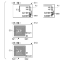
第2実施形態における被検出部50は、2層の配線パターンを含む基板により構成される。図11は、当該被検出部50における第1層および第2層の配線パターンを、信号生成部60からみて透視した状態で示す平面図である。なお、図11においては、容量素子52の図示が便宜的に省略されている。また、図12は、図11におけるC-c線の断面図である。
The part to be detected 50 in the second embodiment is configured by a substrate including two layers of wiring patterns. FIG. 11 is a plan view showing the wiring patterns of the first layer and the second layer in the detected
第2実施形態の被検出部50は、第1層の配線パターン511と、基材551と、第2層の配線パターン512と、基材552とがこの順で積層された積層体である。すなわち、第2実施形態の被検出部50においては、第1実施形態と比較して、第3層の配線パターン513と、基材553と、第4層の配線パターン514とが省略される。
The detected
被検出部50には、ビアC1、C3、C6およびC8が設けられる。これらのビアC1、C3、C6およびC8は、コンタクトホールである。
The detected
第1層の配線パターン511のうち、ビアC1に接続された端子Naと、ビアC8に接続された端子Nbとを含む領域A1には、容量素子52が実装される。
被検出部50の第1コイル51は、第2層の配線パターン512によって構成される。詳細には、第1コイル51は、配線パターン512のうち、渦巻き状に形成された第1部分521と、同方向で渦巻き状に形成された第2部分522とによって構成される。
なお、第2実施形態において、第1部分521における渦巻きの中心はビアC3であり、第2部分522における渦巻きの中心はビアC6である。ビアC3およびビアC6は、配線パターン511の一部である配線515を介して相互に接続される。In the
The
In the second embodiment, the center of the spiral in the
すなわち、第2実施形態において、領域A1内の端子Naは、ビアC1を介して、第2層における第1部分521の一端(ノードN21)に接続される。第1部分521の他端は、ビアC3を介して、第1層における配線515を介してビアC6に接続される。配線515は、ビアC6を介して、第2層における第2部分522に接続される。第2部分522の他端(ノードN22)は、ビアC8を介して、第1層における端子Nbに接続される。
このように第2実施形態の第1コイル51においては、第1部分521および第2部分522が直列接続される。That is, in the second embodiment, the terminal Na in the area A1 is connected to one end (node N21) of the
Thus, in the
第2実施形態は、第1実施形態と比較すると、第1コイル51を構成する部分の総数が半分となるが、磁界の発生方向は第1実施形態と同様である。すなわち、第1部分521と第2部分522とでは互いに逆方向の磁界が発生する。鍵盤10において複数の鍵12は図12の紙面垂直方向に配列するから、相互に隣り合う各鍵12の間にわたる磁界の拡散が低減される。したがって、複数の鍵12の各々の位置Zを高精度に反映した検出信号Dを生成できる。
In the second embodiment, the total number of parts constituting the
第2実施形態では、第1コイル51を構成する第1部分521および第2部分522が基材551および基材552で覆われるので、露出することがない。すなわち、第2実施形態では、基材551および基材552が保護部材として機能するので、第1コイル51が保護される。したがって、第2実施形態においても、工具等による擦れによる当該第1コイル51の損傷が防止される。
また、第2実施形態では、第1実施形態と比較して、第3層の配線パターン513、基材553および第4層の配線パターン514が存在しないので、その分、構成が簡易と成る。
なお、第2実施形態では、基材551が第1絶縁層の一例として機能し、配線パターン512が第1配線パターンの一例として機能し、基材552が第2絶縁層の一例として機能する。基材551および基材552は、保護部材の一例として機能する。In the second embodiment, since the
Further, in the second embodiment, the
In the second embodiment, the
C:第3実施形態
第3実施形態について説明する。第3実施形態における被検出部50は、第1実施形態と同様に、4層の配線パターンを含む基板により構成される。図13は、当該被検出部50における第1層および第2層の配線パターンを、信号生成部60からみて透視した状態で示す平面図である。なお、図13においては、容量素子52の図示が便宜的に省略されている。第3実施形態の被検出部50は、図6に例示した第1実施形態と同様に、第1層の配線パターン511と、基材551と、第2層の配線パターン512と、基材552と、第3層の配線パターン513と、基材553と、第4層の配線パターン514とがこの順で積層された積層体である。C: Third Embodiment A third embodiment will be described. The detected
第3実施形態において、被検出部50の第1コイル51は、第2層の配線パターン512のうち第1部分521と、第3層の配線パターン513のうち第2部分522とによって構成される。第1部分521は、渦巻き状に形成されている。第2部分522は、第1部分521とは逆方向の渦巻き状に形成されている。
なお、第2実施形態において、第1部分521における渦巻きの中心と第2部分522における渦巻きの中心とはビアC3である。すなわち、第3実施形態において、第1部分521と第2部分522とは、ビアC3を介して相互に接続される。In the third embodiment, the
In the second embodiment, the center of the spiral in the
詳細には、第3実施形態において、領域A1内の端子Naは、ビアC1を介して、第2層における第1部分521の一端(ノードN31)に接続される。第1部分521の他端は、ビアC3を介して、第3層における第2部分522の一端に接続される。第2部分522の他端(ノードN32)は、ビアC8を介して、第1層における領域A1内の端子Nbに接続される。
なお、第3実施形態の被検出部50の構造については、第1実施形態の断面図である図6によって十分に類推可能であるので、図示を省略している。Specifically, in the third embodiment, the terminal Na in the area A1 is connected to one end (node N31) of the
It should be noted that the structure of the detected
第3実施形態では、第1実施形態と同様に、第1コイル51を構成する第2部分522が基材552および基材553で覆われるので、露出することがない。すなわち、第3実施形態では、基材552および基材553が保護部材として機能するので、第1コイル51が保護される。したがって、第3実施形態においても、工具等による擦れによる当該第1コイル51の損傷が防止される。
また、第3実施形態は、第1実施形態と比較すると、第1コイル51を構成する部分が半分となるが、第1部分521と第2部分522とは相互に重なって位置し、かつ磁界は同方向に発生する。このため、第3実施形態は、第1実施形態と比較して基板面積がおおよそ半分で済む。すなわち、被検出部50の設置に必要なスペースが削減される。
なお、第3実施形態では、基材551が第1絶縁層の一例として機能し、配線パターン512が第1配線パターンの一例として機能し、基材552が第2絶縁層の一例として機能し、配線パターン513が第2配線パターンの一例として機能し、基材553が第3絶縁層の一例として機能する。基材552および基材553は保護部材の一例として機能する。In the third embodiment, as in the first embodiment, the
Also, in the third embodiment, the portion constituting the
In the third embodiment, the
D:第4実施形態
第4実施形態について説明する。図14は、被検出部50における配線パターンを、信号生成部60からみて透視した状態で示す平面図である。第4実施形態における被検出部50の第1コイル51は、第1部分521または第2部分522の何れかにより構成される。すなわち、被検出部50は、第1コイル51が第1部分521で構成される状態と、第1コイル51が第2部分522で構成される状態との一方から他方に切替えられる。
第1層の表面には、ジャンパースイッチ560が設けられる。ジャンパースイッチ560は、ビアC21またはビアC22の何れかを領域A1内の端子Naに接続するスイッチである。詳細には、端子NaをビアC21に接続する場合には、図において右欄で示されるようにソケットが差し込まれ、端子NaをビアC22に接続する場合には、図において左欄で示されるようにソケットが差し込まれる。D: Fourth Embodiment A fourth embodiment will be described. FIG. 14 is a plan view showing the wiring pattern in the detected
A
なお、ジャンパースイッチ560が右欄で示されるように位置する場合、端子Naは、ビアC21を介して、第2層における第1部分521の一端(ノードN41)に接続される。ジャンパースイッチ560が左欄で示されるように位置する場合、端子Naは、ビアC22を介して、第3層における第2部分522の一端(ノードN42)に接続される。
第1部分521の他端および第2部分522の他端は、共通のビアC3を介して、第1層における領域A1内の端子Nbに接続される。When
The other end of the
第4実施形態では、例えば被検出部50が設置された当初の初期状態では、ジャンパースイッチ560が左欄で示されるように位置して、第2部分522を第1コイル51として機能させる。一方、第2部分522になんらかの不具合が生じたならば、ジャンパースイッチ560を右欄で示される状態に切り替えて、第1部分521を第1コイル51として機能させる。
すなわち、第4実施形態では、第1部分521を予備コイルとし、第2部分522を第1コイル51として機能させる一方で、第2部分522に不具合が生じたならば、ジャンパースイッチ560の切り替えによって、第1部分521を第1コイル51として機能させることができる。In the fourth embodiment, the
That is, in the fourth embodiment, the
以上の説明から理解される通り、第4実施形態の変位センサー20は、可動部材の一例である鍵12に設置された被検出部50と、電流の供給により磁界を発生する第2コイル61を含む信号生成部60とを具備する。被検出部50は、絶縁性樹脂により形成された保護部材(基材551または基材552)で保護された第1部分521と、第3コイルの一例である第2部分522とを含む。ジャンパースイッチ560は、第1部分521が共振回路を構成する第1状態と、第2部分522が共振回路を構成する第2状態とを切替える切替部として機能する。信号生成部60は、被検出部50の共振回路と第2コイル61との相対位置に応じた検出信号を生成する。なお、第2部分522は、保護部材により保護されてもよいし保護されなくてもよい。
As can be understood from the above description, the
第4実施形態では、第2部分522を覆う部材はなくてもよいし、仮に第2部分522が損傷しても、ジャンパースイッチ560を切り替えれば、第1部分521を第1コイル51として機能させることができる。すなわち、第4実施形態では、ジャンパースイッチ560によって第1部分521を第1コイル51として機能させる場合、基材552が保護部材として機能するので、第1コイル51が保護される。
なお、第4実施形態では、基材551が第1絶縁層の一例として機能し、配線パターン512が第1配線パターンの一例として機能し、基材552が第2絶縁層の一例として機能し、配線パターン513が第2配線パターンの一例として機能し、基材553が第3絶縁層の一例として機能する。In the fourth embodiment, there may be no member covering the
In the fourth embodiment, the
E:変形例
以上に例示した各態様に付加される具体的な変形の態様を以下に例示する。以下の例示から任意に選択された2以上の態様を、相互に矛盾しない範囲で適宜に併合してもよい。E: Modifications Examples of specific modifications added to the above-exemplified embodiments are given below. Two or more aspects arbitrarily selected from the following examples may be combined as appropriate within a mutually consistent range.
(1)上述した各形態においては、鍵盤楽器100の鍵12の変位を検出する構成を例示したが、変位センサー20により変位が検出される可動部材は鍵12に限定されない。可動部材の具体的な態様を以下に例示する。
(1) In each of the above embodiments, the configuration for detecting the displacement of the
[態様1]
図15は、鍵盤楽器100の打弦機構91に変位センサー20を適用した構成の模式図である。打弦機構91は、アコースティックピアノと同様に、鍵盤10の各鍵12の変位に連動して弦(図示略)を打撃するアクション機構である。具体的には、打弦機構91は、回動により打弦可能なハンマー911と、鍵12の変位に連動してハンマー911を回動させる伝達機構912(例えばウィペン、ジャック、レペティションレバー等)とを、鍵12毎に具備する。
被検出部50がハンマー911(例えばハンマーシャンク)に設置される。また、信号生成部60は支持部材913に設置される。このような構成において、変位センサー20は、ハンマー911の変位を検出する。具体的には、支持部材913は、例えば打弦機構91を支持する構造体である。なお、被検出部50は、打弦機構91におけるハンマー911以外の可動部材に設置してもよい。[Aspect 1]
FIG. 15 is a schematic diagram of a configuration in which the
A detected
[態様2]
図16は、鍵盤楽器100のペダル機構92に変位センサー20を適用した構成の模式図である。ペダル機構92は、利用者が足で操作するペダル921と、ペダル921を支持する支持部材922と、鉛直方向の上方にペダル921を付勢する弾性体923とを具備する。
被検出部50がペダル921の底面に設置される。また、信号生成部60は、被検出部50に対向するように支持部材922に設置される。このような構成において、変位センサー20はペダル921の変位を検出する。
なお、ペダル機構92が利用される楽器は鍵盤楽器100に限定されない。例えば打楽器等の任意の楽器にも同様の構成のペダル機構92が利用される。[Aspect 2]
FIG. 16 is a schematic diagram of a configuration in which the
A detected
Note that the musical instrument using the
以上の例示から理解される通り、変位センサーによる検出の対象は、演奏動作に応じて変位する可動部材として包括的に表現される。可動部材は、利用者が直接的に操作する鍵12またはペダル921等の演奏操作子のほか、演奏操作子に対する操作に連動して変位するハンマー911等の構造体を含む。ただし、本開示における可動部材は、演奏動作に応じて変位する部材に限定されない。すなわち、可動部材は、変位を発生させる契機に関わらず、変位可能な部材として包括的に表現される。
As can be understood from the above examples, the objects to be detected by the displacement sensor are comprehensively represented as movable members that are displaced according to the performance action. The movable members include performance operators such as the
(2)上述の実施形態においては、被検出部50の表面F1に形成された配線パターン511に表面F1上の容量素子52が接続される構成を例示したが、絶縁層間の配線パターン(512または513)に対して例えばブラインドビアにより表面F1上の容量素子52を接続してもよい。容量素子52が絶縁層間の配線パターンに接続される構成においては、被検出部50から配線パターン511が省略されてもよい。すなわち、被検出部50の表面F1に配線パターン511が存在しない構成も想定される。以上の構成において、設置面122の切欠部124に容量素子52が収容される前述の構成を採用すれば、容量素子52の破損を抑制できるという前述の効果は格別に顕著である。
(2) In the above-described embodiment, the configuration in which the
(3)上述の実施形態においては、基材(552,553)を保護部材として例示したが、保護部材の形態は以上の例示に限定されない。例えば、平板状の基材の表面に形成された絶縁層を「保護部材」として利用してもよい。絶縁層は、例えば防水を目的とした膜体であり、例えばシリコン,エポキシまたはウレタン等の絶縁材料により形成される。絶縁層の形成には、例えばコーティングまたはポッティング等の各種の加工技術が利用される。以上の説明から理解される通り、「保護部材」は、独立した基材のほか、基材の表面を被覆する膜体も含む概念である。 (3) In the above-described embodiments, the substrates (552, 553) were exemplified as protective members, but the form of the protective member is not limited to the above examples. For example, an insulating layer formed on the surface of a flat substrate may be used as the "protective member". The insulating layer is, for example, a film intended for waterproofing, and is formed of an insulating material such as silicon, epoxy, or urethane. Various processing techniques, such as coating or potting, are used to form the insulating layer. As understood from the above description, the concept of "protective member" includes not only an independent base material but also a film body covering the surface of the base material.
(4)前述の各形態においては、鍵盤楽器100が音源回路34を具備する構成を例示したが、例えば鍵盤楽器100が打弦機構91等の発音機構を具備する構成においては、音源回路34を省略してもよい。検出システム15は、鍵盤楽器100の演奏内容を記録するために利用される。発音機構および音源回路34は、検出システム15による検出の結果に応じて音を生成する音生成部として包括的に表現される。
(4) In each of the above-described embodiments, the
以上の説明から理解される通り、本開示は、音源回路34または発音機構に対して演奏動作に応じた操作信号を出力することで楽音を制御する装置(演奏操作装置)としても特定される。前述の各形態の例示のように音源回路34または発音機構を具備する楽器(鍵盤楽器100)のほか、音源回路34または発音機構を具備しない機器(例えばMIDIコントローラまたは前述のペダル機構92)が、演奏操作装置(instrument playing apparatus)の概念には包含される。すなわち、本開示における演奏操作装置は、演奏者(操作者)が演奏のために操作する装置として包括的に表現される。
As can be understood from the above description, the present disclosure is also specified as a device (performance operation device) that controls musical tones by outputting operation signals corresponding to performance operations to the
(5)上述の実施形態においては、本開示の保護部材として、表面全体をすべて樹脂層で覆う構成として示したが、必ずしも全体を覆っていなくてもよい。例えば、保護部材を網状の部材でパターンを覆うようにしてもよい。また、角柱状の部材を基板の長手あるいは短手方向に部材間の間隔を開けずに、あるいは所定の間隔で並べて配置するようにしてもよい。また、コイルパターンの部分だけを保護部材で覆うようにしてもよい。 (5) In the above-described embodiments, the protective member of the present disclosure has a configuration in which the entire surface is covered with a resin layer, but the entire surface may not necessarily be covered. For example, the protective member may be a mesh-like member covering the pattern. Also, the prismatic members may be arranged side by side in the longitudinal direction or the lateral direction of the substrate with no gap between the members or with a predetermined gap. Alternatively, only the coil pattern portion may be covered with the protective member.
F:付記
上述した実施形態等から、例えば以下のような態様が把握される。F: Supplementary Note The following aspects, for example, can be understood from the above-described embodiments and the like.
本開示の態様(第1態様)に係る変位センサーは、操作に応じた可動部材の変位を検出する変位センサーであって、前記可動部材に設置され、絶縁性樹脂により形成された保護部材で保護された第1コイルを含む被検出部と、電流の供給により磁界を発生する第2コイルを含み、前記被検出部の第1コイルとそれに対向する前記第2コイルとの相対位置に応じた検出信号を生成する信号生成部と、を具備する。
この態様によれば、第1コイルが保護部材で保護されるので、第1コイルが擦れ等による損傷してしまうことを防止できる。A displacement sensor according to an aspect (first aspect) of the present disclosure is a displacement sensor that detects displacement of a movable member according to an operation, and is installed on the movable member and protected by a protective member made of insulating resin. and a second coil that generates a magnetic field when supplied with a current, and detection according to the relative position of the first coil of the detected part and the second coil facing it and a signal generator that generates a signal.
According to this aspect, since the first coil is protected by the protective member, it is possible to prevent the first coil from being damaged due to rubbing or the like.
前記第1態様の例(第2態様)において、前記第2コイルの中心軸の方向における前記第1コイルと前記第2コイルとの距離が、前記可動部材の変位に応じて変化する。
この態様によれば、第2コイルの中心軸に垂直な面内において被検出部と第2コイルとが相対的に移動する構成(すなわち、第2コイルの中心軸の方向における被検出部と第2コイルとの距離は変化しない構成)と比較して、可動部材の変位に対して検出信号のレベルを大きく変化させることが可能である。In the example of the first aspect (second aspect), the distance between the first coil and the second coil in the direction of the central axis of the second coil changes according to the displacement of the movable member.
According to this aspect, the detected portion and the second coil move relatively in a plane perpendicular to the central axis of the second coil (that is, the detected portion and the second coil move in the direction of the central axis of the second coil). Compared to the configuration in which the distance to the two coils does not change), it is possible to greatly change the level of the detection signal with respect to the displacement of the movable member.
第1または第2態様の例(第3態様)において、前記被検出部は、前記第1コイルに接続される容量素子を含む。この態様によれば、容量素子の容量に応じて、第1コイルおよび容量素子による共振周波数を調整できる、という利点がある。 In the example of the first or second aspect (third aspect), the detected part includes a capacitive element connected to the first coil. According to this aspect, there is an advantage that the resonance frequency by the first coil and the capacitive element can be adjusted according to the capacitance of the capacitive element.
第3態様の例(第4態様)において、前記可動部材は、前記被検出部が設置される設置面を有し、前記設置面には切欠部が設けられ、前記容量素子が前記切欠部に収容された状態で、前記被検出部が前記可動部材に設置される。
この態様によれば、基板に実装される容量素子が露出しないので、容量素子が、例えばメンテナンス等において他の部材に引っかかることで破損してしまうことを防止できる。In the example of the third aspect (fourth aspect), the movable member has an installation surface on which the detected part is installed, the installation surface is provided with a notch, and the capacitive element is provided in the notch. The part to be detected is installed on the movable member in the accommodated state.
According to this aspect, since the capacitive element mounted on the substrate is not exposed, it is possible to prevent the capacitive element from being damaged by being caught by other members during maintenance or the like.
第1乃至第4態様の何れかの例(第5態様)において、前記被検出部は、少なくとも第1絶縁層、第1配線パターンおよび第2絶縁層を含み、前記第1配線パターンが、前記第1絶縁層および前記第2絶縁層の間に位置し、前記第1コイルは、前記第1配線パターンに含まれる渦巻き形状の部分である。
この態様によれば、例えば第1コイルを導電線の巻回により形成する構成と比較して、第1コイルの製造および取扱が容易であるという利点がある。In any example of the first to fourth aspects (fifth aspect), the part to be detected includes at least a first insulating layer, a first wiring pattern and a second insulating layer, and the first wiring pattern includes the Located between the first insulating layer and the second insulating layer, the first coil is a spiral portion included in the first wiring pattern.
According to this aspect, there is an advantage that the first coil is easy to manufacture and handle, compared with a configuration in which the first coil is formed by winding a conductive wire, for example.
第1乃至第4態様の何れかの例(第6態様)において、前記被検出部は、少なくとも第1絶縁層、第1配線パターン、第2絶縁層、第2配線パターンおよび第3絶縁層を含み、前記第1配線パターンが、前記第1絶縁層および前記第2絶縁層の間に位置し、前記第2配線パターンが、前記第2絶縁層および前記第3絶縁層の間に位置し、前記第1コイルは、第1部分と第2部分と第3部分と第4部分とを含み、前記第1部分および前記第4部分は、前記第1配線パターンに含まれる渦巻き形状の部分であり、前記第2部分および前記第3部分は、前記第2配線パターンに含まれる渦巻き形状の部分であり、前記第1部分と前記第2部分とは平面視で相互に重なり、前記第3部分と前記第4部分とは平面視で相互に重なり、前記第1部分により生成される磁界と前記第2部分により生成される磁界とは、第1方向であり、前記第3部分により生成される磁界と前記第4部分により生成される磁界とは、前記第1方向とは逆方向の第2方向である。
この態様によれば、第1部分と第2部分とに第1方向の磁界が発生し、第3部分と第4部分とに第1方向とは逆方向の磁界が発生するので、第1コイルから周囲に対する磁界の拡散が低減される。したがって、相異なる可動部材に対応する複数の第1コイルが相互に近接する構成において、複数の可動部材の各々の変位を高精度に反映した検出信号を生成できる。In any example of the first to fourth aspects (sixth aspect), the part to be detected includes at least a first insulating layer, a first wiring pattern, a second insulating layer, a second wiring pattern and a third insulating layer. wherein the first wiring pattern is located between the first insulating layer and the second insulating layer, the second wiring pattern is located between the second insulating layer and the third insulating layer, The first coil includes a first portion, a second portion, a third portion, and a fourth portion, and the first portion and the fourth portion are spiral-shaped portions included in the first wiring pattern. , the second portion and the third portion are spiral-shaped portions included in the second wiring pattern, the first portion and the second portion overlap each other in a plan view, and the third portion and the The fourth portion overlaps with each other in plan view, the magnetic field generated by the first portion and the magnetic field generated by the second portion are in the first direction, and the magnetic field generated by the third portion and the magnetic field generated by the fourth portion is in a second direction opposite to the first direction.
According to this aspect, a magnetic field in the first direction is generated in the first portion and the second portion, and a magnetic field in the direction opposite to the first direction is generated in the third portion and the fourth portion, so that the first coil from the spread of the magnetic field to the surroundings is reduced. Therefore, in a configuration in which a plurality of first coils corresponding to different movable members are close to each other, it is possible to generate a detection signal reflecting the displacement of each of the plurality of movable members with high accuracy.
なお、「平面視」とは、配線パターンの表面に垂直な方向に沿って観察すること、または、絶縁層の表面に垂直な方向からみて観察することを意味する。第1コイルの軸方向に沿って観察することを「平面視」と表現してもよい。 Note that "planar view" means observing along a direction perpendicular to the surface of the wiring pattern, or observing from a direction perpendicular to the surface of the insulating layer. Observation along the axial direction of the first coil may be expressed as "plan view".
第1乃至第4態様の何れかの例(第7態様)において、前記被検出部は、少なくとも第1絶縁層、第1配線パターンおよび第2絶縁層を含み、前記第1配線パターンが、前記第1絶縁層および前記第2絶縁層の間に位置し、前記第1コイルは、第1部分と第2部分とを含み、前記第1部分および前記第2部分は、前記第1配線パターンに含まれる渦巻き形状の部分であり、前記第1部分により生成される磁界と前記第2部分により生成される磁界とは、相互に逆方向である。
この態様によれば、第1部分と第2部分とは、平面視で重なり、発生磁界が同方向であるので、第1部分または第2部分の単体と比較して磁界の強さを大きくすることができる。In any example of the first to fourth aspects (seventh aspect), the detected portion includes at least a first insulating layer, a first wiring pattern, and a second insulating layer, and the first wiring pattern includes the Positioned between a first insulating layer and the second insulating layer, the first coil includes a first portion and a second portion, the first portion and the second portion being connected to the first wiring pattern. A spiral-shaped portion is included, wherein the magnetic field generated by the first portion and the magnetic field generated by the second portion are in opposite directions to each other.
According to this aspect, the first portion and the second portion overlap in plan view, and the generated magnetic field is in the same direction. be able to.
第1乃至第4態様の何れかの例(第8態様)において、前記被検出部は、少なくとも第1絶縁層、第1配線パターン、第2絶縁層、第2配線パターンおよび第3絶縁層を含み、前記第1配線パターンが、前記第1絶縁層および前記第2絶縁層の間に位置し、前記第2配線パターンが、前記第2絶縁層および前記第3絶縁層の間に位置し、前記第1コイルは、第1部分と第2部分とを含み、前記第1部分は、前記第1配線パターンに含まれる渦巻き形状の部分であり、前記第2部分は、前記第2配線パターンに含まれる渦巻き形状の部分であり、前記第1部分および前記第2部分は平面視で相互に重なり、前記第1部分により生成される磁界と前記第2部分により生成される磁界とは、相互に同方向である。
この態様によれば、第1部分と第2部分とが平面視で重なるので、被検出部の設置に必要なスペースが削減される。In any example of the first to fourth aspects (eighth aspect), the part to be detected includes at least a first insulating layer, a first wiring pattern, a second insulating layer, a second wiring pattern and a third insulating layer. wherein the first wiring pattern is located between the first insulating layer and the second insulating layer, the second wiring pattern is located between the second insulating layer and the third insulating layer, The first coil includes a first portion and a second portion, the first portion being a spiral-shaped portion included in the first wiring pattern, and the second portion being in the second wiring pattern. spiral-shaped portion included, the first portion and the second portion overlap each other in plan view, and the magnetic field generated by the first portion and the magnetic field generated by the second portion overlap each other in the same direction.
According to this aspect, since the first portion and the second portion overlap in a plan view, the space required for installing the detected portion can be reduced.
第1乃至第4態様の何れかの例(第9態様)において、前記被検出部は、第3コイルと、前記第1コイルが共振回路を構成する第1状態と、前記第3コイルが共振回路を構成する第2状態とを切替える切替部とを含む。この態様によれば、他のコイルが損傷しても、当該他のコイルを、保護部材で保護された第1コイルに置き換えて使用することができる。 In any one of the first to fourth aspects (the ninth aspect), the part to be detected includes a third coil, a first state in which the first coil forms a resonance circuit, and a state in which the third coil resonates. a switching unit for switching between a second state and a second state forming a circuit; According to this aspect, even if another coil is damaged, the other coil can be used by replacing it with the first coil protected by the protective member.
本開示のひとつの態様(第10態様)に係る演奏操作装置は、第1乃至第9態様の何れかに記載の変位センサーと、前記検出信号のレベルに応じた音を表す音響信号を生成する音制御部とを具備する。 A performance operating device according to one aspect (tenth aspect) of the present disclosure includes the displacement sensor according to any one of the first to ninth aspects, and generates an acoustic signal representing a sound according to the level of the detection signal. and a sound controller.
100…鍵盤楽器(演奏操作装置)、10…鍵盤、12…鍵、15…検出システム、20…変位センサー、21…信号処理回路、22…供給回路、23…出力回路、30…情報処理装置、50…被検出部、51…第1コイル、52…容量素子、521…第1部分、522…第2部分、523…第3部分、524…第4部分、551、552、553…基材。
DESCRIPTION OF
Claims (10)
前記可動部材の設置面に設置された被検出部であって、絶縁性樹脂により形成された保護部材と、前記保護部材で保護された第1コイルと、前記第1コイルに接続される容量素子とを含む被検出部と、
電流の供給により磁界を発生する第2コイルを含み、前記被検出部の前記第1コイルとそれに対向する前記第2コイルとの相対位置に応じた検出信号を生成する信号生成部と、
を具備し、
前記設置面に形成された切欠部に前記容量素子が収容された状態で、前記被検出部が前記可動部材に設置される
変位センサー。 A displacement sensor that detects displacement of a movable member according to an operation,
A detection target portion installed on an installation surface of the movable member, the protection member being formed of an insulating resin , a first coil protected by the protection member , and a capacitive element connected to the first coil. and a detected part including
a signal generator that includes a second coil that generates a magnetic field when supplied with a current and that generates a detection signal according to the relative position of the first coil of the detected portion and the second coil facing the first coil;
and
The part to be detected is installed on the movable member in a state in which the capacitive element is accommodated in the notch formed in the installation surface.
displacement sensor.
請求項1に記載の変位センサー。 The part to be detected is installed on the movable member in a state in which the surface of the protective member is in contact with the installation surface and the capacitive element protruding from the surface of the protective member is accommodated in the notch. Item 1. The displacement sensor according to item 1.
請求項1または請求項2に記載の変位センサー。 3. The displacement sensor according to claim 1, wherein the distance between the first coil and the second coil in the direction of the central axis of the second coil changes according to the displacement of the movable member.
少なくとも第1絶縁層、第1配線パターンおよび第2絶縁層を含み、
前記第1配線パターンが、前記第1絶縁層および前記第2絶縁層の間に位置し、
前記第1コイルは、前記第1配線パターンに含まれる渦巻き形状の部分である
請求項1から請求項3の何れかに記載の変位センサー。 The part to be detected is
including at least a first insulating layer, a first wiring pattern and a second insulating layer;
the first wiring pattern is located between the first insulating layer and the second insulating layer;
The displacement sensor according to any one of claims 1 to 3, wherein the first coil is a spiral portion included in the first wiring pattern.
少なくとも第1絶縁層、第1配線パターン、第2絶縁層、第2配線パターンおよび第3絶縁層を含み、
前記第1配線パターンが、前記第1絶縁層および前記第2絶縁層の間に位置し、
前記第2配線パターンが、前記第2絶縁層および前記第3絶縁層の間に位置し、
前記第1コイルは、第1部分と第2部分と第3部分と第4部分とを含み、
前記第1部分および前記第4部分は、前記第1配線パターンに含まれる渦巻き形状の部分であり、
前記第2部分および前記第3部分は、前記第2配線パターンに含まれる渦巻き形状の部分であり、
前記第1部分と前記第2部分とは平面視で相互に重なり、
前記第3部分と前記第4部分とは平面視で相互に重なり、
前記第1部分により生成される磁界と前記第2部分により生成される磁界とは、第1方向であり、
前記第3部分により生成される磁界と前記第4部分により生成される磁界とは、前記第1方向とは逆方向の第2方向である
請求項1から請求項3の何れかに記載の変位センサー。 The part to be detected is
including at least a first insulating layer, a first wiring pattern, a second insulating layer, a second wiring pattern and a third insulating layer;
the first wiring pattern is located between the first insulating layer and the second insulating layer;
the second wiring pattern is located between the second insulating layer and the third insulating layer;
the first coil includes a first portion, a second portion, a third portion, and a fourth portion;
The first portion and the fourth portion are spiral-shaped portions included in the first wiring pattern,
the second portion and the third portion are spiral-shaped portions included in the second wiring pattern;
the first portion and the second portion overlap each other in plan view;
the third portion and the fourth portion overlap each other in plan view,
the magnetic field generated by the first portion and the magnetic field generated by the second portion are in a first direction;
The displacement according to any one of claims 1 to 3, wherein the magnetic field generated by the third portion and the magnetic field generated by the fourth portion are in a second direction opposite to the first direction. sensor.
少なくとも第1絶縁層、第1配線パターンおよび第2絶縁層を含み、
前記第1配線パターンが、前記第1絶縁層および前記第2絶縁層の間に位置し、
前記第1コイルは、第1部分と第2部分とを含み、
前記第1部分および前記第2部分は、前記第1配線パターンに含まれる渦巻き形状の部分であり、
前記第1部分により生成される磁界と前記第2部分により生成される磁界とは、相互に逆方向である
請求項1から請求項3の何れかに記載の変位センサー。 The part to be detected is
including at least a first insulating layer, a first wiring pattern and a second insulating layer;
the first wiring pattern is located between the first insulating layer and the second insulating layer;
the first coil includes a first portion and a second portion;
The first portion and the second portion are spiral-shaped portions included in the first wiring pattern,
4. The displacement sensor according to any one of claims 1 to 3, wherein the magnetic field generated by the first portion and the magnetic field generated by the second portion are opposite to each other.
少なくとも第1絶縁層、第1配線パターン、第2絶縁層、第2配線パターンおよび第3絶縁層を含み、
前記第1配線パターンが、前記第1絶縁層および前記第2絶縁層の間に位置し、
前記第2配線パターンが、前記第2絶縁層および前記第3絶縁層の間に位置し、
前記第1コイルは、第1部分と第2部分とを含み、
前記第1部分は、前記第1配線パターンに含まれる渦巻き形状の部分であり、
前記第2部分は、前記第2配線パターンに含まれる渦巻き形状の部分であり、
前記第1部分および前記第2部分は平面視で相互に重なり、
前記第1部分により生成される磁界と前記第2部分により生成される磁界とは、相互に同方向である
請求項1から請求項3の何れかに記載の変位センサー。 The part to be detected is
including at least a first insulating layer, a first wiring pattern, a second insulating layer, a second wiring pattern and a third insulating layer;
the first wiring pattern is located between the first insulating layer and the second insulating layer;
the second wiring pattern is located between the second insulating layer and the third insulating layer;
the first coil includes a first portion and a second portion;
The first portion is a spiral-shaped portion included in the first wiring pattern,
The second portion is a spiral-shaped portion included in the second wiring pattern,
the first portion and the second portion overlap each other in plan view;
The displacement sensor according to any one of claims 1 to 3 , wherein the magnetic field generated by the first portion and the magnetic field generated by the second portion are in the same direction.
前記可動部材に設置された被検出部であって、絶縁性樹脂により形成された保護部材で保護された第1コイルと、第3コイルと、前記第1コイルが共振回路を構成する第1状態と前記第3コイルが共振回路を構成する第2状態とを切替える切替部とを含む被検出部と、
電流の供給により磁界を発生する第2コイルを含み、前記被検出部の前記第1コイルとそれに対向する前記第2コイルとの相対位置に応じた検出信号を生成する信号生成部と、
を具備する変位センサー。 A displacement sensor that detects displacement of a movable member according to an operation,
A first state in which a first coil, a third coil, and the first coil, which is a detected portion provided on the movable member and protected by a protective member made of an insulating resin, constitutes a resonance circuit. and a detecting portion including a switching portion for switching between and a second state in which the third coil forms a resonant circuit ;
a signal generator that includes a second coil that generates a magnetic field when supplied with a current and that generates a detection signal according to the relative position of the first coil of the detected portion and the second coil facing the first coil;
a displacement sensor.
請求項8の変位センサー。 9. The displacement sensor of claim 8.
前記検出信号のレベルに応じた音を表す音響信号を生成する音制御部と、
を具備する演奏操作装置。
a displacement sensor according to any one of claims 1 to 9 ;
a sound control unit that generates an acoustic signal representing a sound corresponding to the level of the detection signal;
A performance operation device comprising
Applications Claiming Priority (3)
| Application Number | Priority Date | Filing Date | Title |
|---|---|---|---|
| JP2020042520 | 2020-03-12 | ||
| JP2020042520 | 2020-03-12 | ||
| PCT/JP2021/009027 WO2021182409A1 (en) | 2020-03-12 | 2021-03-08 | Displacement sensor and performance operation device |
Publications (3)
| Publication Number | Publication Date |
|---|---|
| JPWO2021182409A1 JPWO2021182409A1 (en) | 2021-09-16 |
| JPWO2021182409A5 JPWO2021182409A5 (en) | 2022-11-11 |
| JP7327646B2 true JP7327646B2 (en) | 2023-08-16 |
Family
ID=77670885
Family Applications (1)
| Application Number | Title | Priority Date | Filing Date |
|---|---|---|---|
| JP2022507186A Active JP7327646B2 (en) | 2020-03-12 | 2021-03-08 | Displacement sensor and performance control device |
Country Status (3)
| Country | Link |
|---|---|
| JP (1) | JP7327646B2 (en) |
| CN (1) | CN218297031U (en) |
| WO (1) | WO2021182409A1 (en) |
Families Citing this family (1)
| Publication number | Priority date | Publication date | Assignee | Title |
|---|---|---|---|---|
| GB2570533B (en) * | 2017-12-20 | 2021-09-22 | Sonuus Ltd | Keyboard sensor systems and methods |
Citations (4)
| Publication number | Priority date | Publication date | Assignee | Title |
|---|---|---|---|---|
| JP2000149211A (en) | 1998-05-07 | 2000-05-30 | Canon Inc | Plane coil parts for magnetic head, magneto-optical recording magnetic head and magneto-optical recorder |
| JP2002110422A (en) | 2000-09-28 | 2002-04-12 | Murata Mfg Co Ltd | Chip coil parts |
| JP2010122012A (en) | 2008-11-18 | 2010-06-03 | Jtekt Corp | Substrate type double layer coil and displacement sensor apparatus |
| WO2019122867A1 (en) | 2017-12-20 | 2019-06-27 | Sonuus Limited | Keyboard sensor systems and methods |
-
2021
- 2021-03-08 CN CN202190000320.0U patent/CN218297031U/en active Active
- 2021-03-08 WO PCT/JP2021/009027 patent/WO2021182409A1/en active Application Filing
- 2021-03-08 JP JP2022507186A patent/JP7327646B2/en active Active
Patent Citations (4)
| Publication number | Priority date | Publication date | Assignee | Title |
|---|---|---|---|---|
| JP2000149211A (en) | 1998-05-07 | 2000-05-30 | Canon Inc | Plane coil parts for magnetic head, magneto-optical recording magnetic head and magneto-optical recorder |
| JP2002110422A (en) | 2000-09-28 | 2002-04-12 | Murata Mfg Co Ltd | Chip coil parts |
| JP2010122012A (en) | 2008-11-18 | 2010-06-03 | Jtekt Corp | Substrate type double layer coil and displacement sensor apparatus |
| WO2019122867A1 (en) | 2017-12-20 | 2019-06-27 | Sonuus Limited | Keyboard sensor systems and methods |
Also Published As
| Publication number | Publication date |
|---|---|
| WO2021182409A1 (en) | 2021-09-16 |
| CN218297031U (en) | 2023-01-13 |
| JPWO2021182409A1 (en) | 2021-09-16 |
Similar Documents
| Publication | Publication Date | Title |
|---|---|---|
| US11922912B2 (en) | Instrument playing apparatus | |
| JP7302739B2 (en) | Displacement sensors and electronic instruments | |
| US20220277717A1 (en) | Detection system, musical instrument playing apparatus, and musical keyboard instrument | |
| JP7327646B2 (en) | Displacement sensor and performance control device | |
| WO2022075102A1 (en) | Circuit board and detection system | |
| US20230386442A1 (en) | Detection system and keyboard instrument | |
| US20220277719A1 (en) | Musical instrument playing apparatus and musical keyboard instrument | |
| JP2010113027A (en) | Electronic keyboard instrument | |
| JP7290926B2 (en) | electronic musical instrument | |
| WO2023228746A1 (en) | Detection system and musical instrument | |
| US20240078984A1 (en) | Detection system for musical instrument and musical instrument | |
| WO2023228745A1 (en) | Detection system and musical instrument | |
| WO2022244721A1 (en) | Musical instrument | |
| JP6638991B2 (en) | Stringed instrument | |
| JP2621674B2 (en) | Chord designation device and electronic musical instrument with chord pronunciation function using the device | |
| JP2023087066A (en) | Detection system and performance operation device | |
| JPH0798585A (en) | Electronic stringed instrument | |
| JP2006330768A (en) | Player |
Legal Events
| Date | Code | Title | Description |
|---|---|---|---|
| A521 | Request for written amendment filed |
Free format text: JAPANESE INTERMEDIATE CODE: A523 Effective date: 20220901 |
|
| A621 | Written request for application examination |
Free format text: JAPANESE INTERMEDIATE CODE: A621 Effective date: 20220901 |
|
| TRDD | Decision of grant or rejection written | ||
| A01 | Written decision to grant a patent or to grant a registration (utility model) |
Free format text: JAPANESE INTERMEDIATE CODE: A01 Effective date: 20230704 |
|
| A61 | First payment of annual fees (during grant procedure) |
Free format text: JAPANESE INTERMEDIATE CODE: A61 Effective date: 20230717 |
|
| R151 | Written notification of patent or utility model registration |
Ref document number: 7327646 Country of ref document: JP Free format text: JAPANESE INTERMEDIATE CODE: R151 |